voltage and current-mode control for a buck-converter based on measured integral values of voltage...
TRANSCRIPT
6686 IEEE TRANSACTIONS ON POWER ELECTRONICS, VOL. 29, NO. 12, DECEMBER 2014
Voltage and Current-Mode Control for aBuck-Converter based on Measured Integral Values
of Voltage and Current Implemented in FPGAMitja Truntic and Miro Milanovic, Member, IEEE
Abstract—This paper describes a complete digitally controlleddc–dc buck converter performed by field-programmable gate ar-ray (FPGA) circuitry. The voltage and current-mode control isbased on a voltage control oscillator (VCO) performed measure-ments regarding output-voltage and inductor current, respectively.This measurement principle also uses digital-counters (digital-integrators) in order to obtain integral values for the output-voltage and inductor current. In analog current-mode control, theinstantaneous inductor current-value-measurement is used for theswitching action. When the VCO is used for the inductor currentmeasurement, the integral is measured during the switching-ontime set as an observation interval and the switching action occursbased on this measurement. Such a principle enables full digital-ization of the voltage- and current-control loop and also the usedmeasurement principle is capable of rejecting the switching distur-bances during current and voltage measurements. All the tasks forcurrent and voltage control were implemented within the FPGA.The algorithm was verified by simulation and experimentation ata switching-frequency of 25 kHz.
Index Terms—Current- and voltage-mode control, field-programmable gate array (FPGA), multiphase buck converter,synchronous buck converter, voltage control oscillator (VCO).
I. INTRODUCTION
D IGITALLY-CONTROLLED pulse-width modulation(PWM) converters have several potential advantages, in-
cluding programmability, insensitivity to parameter variations,reduction of external passive components, as well as the po-tential for applying more advanced algorithms for control andprotection. Further advances in digital technology promptedsome research groups to use field-programmable gate array’s(FPGA’s) or digital signal processors (DSP’s) [1]–[14]. An in-teresting approach where the advantages of digitalization wereused is described in [11], where the authors suggest a combi-nation of linear and nonlinear controllers. The nonlinear con-troller is activated during the load transient. It is only possi-ble to solve such an approach within a digital environment,as are FPGAs. The FPGAs’ applications are well-described inthe survey [15], where the authors addressed various research
Manuscript received September 11, 2013; revised December 5, 2013; ac-cepted January 14, 2014. Date of publication January 21, 2014; date of currentversion August 13, 2014. Recommended for publication by Associate EditorJ. A. Cobos.
The authors are with the University of Maribor FERI, Smetanova 17, SI-2000,Slovenia (e-mail: [email protected]; [email protected]).
Color versions of one or more of the figures in this paper are available onlineat http://ieeexplore.ieee.org.
Digital Object Identifier 10.1109/TPEL.2014.2301935
fields which could exploit the advantages of FPGAs. Usually,the voltage control-loop is superior and is solved by a conven-tional PI controller whereby the reference current is generatedfor the inferior current-control-loop. The current-mode controlproposed in [21] suggests that the switch or the inductor cur-rent should be measured within an inner loop, and replaces theconventional PI controller and saw-tooth generator that are nec-essary for the PWM function. Such algorithms have been usedwithin the domain of the analog solution but, recently, some al-gorithms have been developed based mainly on an instantaneouscurrent measurement and prediction strategy [16]. An interest-ing approach is also discussed in [17], where the authors usedtwo timers (counters) and a studied bifrequency approach forgenerating the triggering pulses within a discontinuous currentmode (DCM) buck-converter’s operation in order to improvethe efficiency of the light mode of operation. According to thedigital-control approach, the inductor-current was sampled atleast twice, when the current was rising (within a Ton inter-val) or falling (within a Toff interval), as discussed in [18]. Thepeak or valley current-mode control could be applied by usingsuch an algorithm. The application of this method is subject todisturbances that may arise when measuring instantaneous in-ductor current signals. Some digitalization principles were alsoperformed in [7] and [9]. In [7], the authors discussed a digitalcircuit based on a digital current-injected control principle inorder to realize the over-current limiting characteristics for adigitally-controlled dc–dc converter, and in [9] also describedthe usage of a voltage control oscillator (VCO) for A/D conver-sion with a DSP unit used for control purposes and triggeringpulse generation.
This paper explores a digital voltage and current-mode con-trol for a dc–dc buck converter based on the measured integralsunder current and voltage curves during Ton (switching-ON) andTs (sampling time) intervals, respectively. The output-voltageand inductor current measurements are performed using VCOsand digital counters. These VCOs and digital counters also havethe function of first-order noise shaping that appear in the mea-sured current and voltage signals because the VCO output isproportional to the time integral of the applied input voltage.In [10], the authors presented current mode control as an in-ternal loop within the voltage-control loop. The average switchcurrent was measured using VCO and used for the control ofdc–dc converters. The authors did not consider the converterfor operating as a current source, which is the main contribu-tion of this presented paper. An average frequency value duringthe switch-on time is considered and presented for the average
0885-8993 © 2014 IEEE. Personal use is permitted, but republication/redistribution requires IEEE permission.See http://www.ieee.org/publications standards/publications/rights/index.html for more information.

TRUNTIC AND MILANOVIC: VOLTAGE AND CURRENT-MODE CONTROL FOR A BUCK-CONVERTER 6687
switch-current control. The instantaneous frequency value dur-ing the switch-on time must also be used in order to performthe instantaneous inductor-peak-current control. The instanta-neous inductor-peak-current control is so performed by usingthe measured area (integral) below the current curve, whereby itis necessary to introduce the so-called dynamic reference (DR).Such an approach enables the inductor-peak-current control asknown from the analog control technique.
Section II presents the operating principle with a theoreti-cal analysis of the areas (integrals) measurement regarding thevoltage and current and explains the necessity for DR calcu-lation. Special emphasis is dedicated to the VCO’s resolutionanalysis, which shows that the chosen VCO produces the appro-priate signals for control purposes. The VCO’s resolution canbe improved as suggested in [12].
Section III considers current and voltage control-loop model-ing based on the PWM switching approach [19], [20], and [21],where the design for the PI controller parameters is performedbased on the modeling in the section. The experimental setupsare described in Section IV, where the test-bench system withFPGA implementation of the whole system is discussed regard-ing signal conditioning, voltage and current-controllers, and thenecessary synchronization procedure. Some verification of theclosed-loop current-mode control and voltage-mode control isperformed by simulation, where the response to a step currentchange is considered. This section concludes with the exper-imental setup results using current-mode control and voltage-mode control during start-up, load change, and also during theinput voltage change for two buck converters. The first one isused to verify all aspects of operational condition. For this pur-pose, a synchronous buck converter of 7.5 W is designed. Thecontrol principle is further applied on four-phase buck convertertested up to 6 kW.
II. PRINCIPLE OF OPERATION
Block diagrams of a voltage and current-mode control schemeregarding the buck converter, is shown in Fig. 1(a). The currentreference Fir is obtained as an output signal of the voltage con-troller. The conventional PI controller and the saw-tooth wave-form generator, which is usually used to generate the PWMsignal, is replaced with an inner current-loop modulator (con-troller). The digitalization principle considered here enablesand/or also provides the inductor current’s information duringthe sampling interval. Digitalization based on measurement ofthe area under the voltage and current curves is performed by us-ing VCOs and digital counters [see Fig. 1(b)]. These componentsare used instead of classical A/D converters. The synchronousbuck is used in order to avoid nonlinearity operation during thediscontinuous current-mode operation.
A. Time-Based Analog to Digital Conversion
Two A/D conversions of the measured signals are requiredfor the voltage and current-mode control as shown in Fig. 1(a).The time-based A/D converter uses a VCO where the frequencyis controlled by the analog input voltage Vin and a counter witha register at its output [see Fig. 1(b)]. The output F is propor-
Fig. 1. (a) Voltage- and current-mode control scheme for buck converter;(b) VCO based A/D conversion architecture.
tional to the time integral of the applied input voltage duringthe sampling period and can be represented by the followingequation:
F =∫ ts 2
ts 1
fvco dt =∫ ts 2
ts 1
(kvcoVin(t) + f0) dt (1)
where the kvco [Hz/V ] is voltage-to-frequency gain, ts1 , ts2 arethe sampling times, and fo is the free-running frequency of theVCO when Vin = 0 V. The resulting VCO output F (t) is fedto a quantizer the digital output of which is the function of aapplied analog input voltage Vin . The quantizer can be imple-mented using a counter which detects the rising edges of theVCO output, thereby quantizing the output. Since the full scaleof the A/D converter input is determined by the maximum fre-quency difference of the VCO output, the resolution of the A/Dconverter that uses a counter as a quantizer can be representedby the following equation:
Resolution = log2
(fmax
fs− fmin
fs
)(2)
where the fmax and fmin are the maximum and minimum op-erating frequencies of the VCO output, respectively. For cor-rect A/D conversion, the sampling frequency should not exceedfs < fmin , which presents the maximum frequency range orthe minimum time duration to set 1-LSB(least significant bit).It can be seen that the resolution is determined by the tuningrange for a sampling rate. The TLC2933A VCO of Texas Instru-ments is further described in the paper and was used for practicalimplementation. The voltage-to-frequency characteristic of thechosen VCO is shown in Fig. 2(a), where the free-running fre-quency is set at f0 = 23.5 MHz with a voltage-to-frequency

6688 IEEE TRANSACTIONS ON POWER ELECTRONICS, VOL. 29, NO. 12, DECEMBER 2014
(a) (b)
Fig. 2. (a) Static characteristic of VCO; (b) resolution versus samplingfrequency.
gain of kvco = 44.1 MHz/V. Two different sampling rates arechosen for the measurements. The first sampling frequency ofoutput-voltage measurement is fixed and is close to the switch-ing frequency set to fs = 25 kHz, where 12-bit resolution ofA/D conversion is achieved. In contrast, the sampling frequencyof the inductor current measurement varies and depends on theswitch-on Ton time interval, whereby the resolution of 12-bitor lower can be achieved. The A/D conversion resolution dropsdown to nine-bit at the sampling interval 1/10 of the switchingperiod Ts , as shown in Fig. 2(b). The switching frequency andVCO operating range are chosen accordingly.
In order to justify the use of VCO instead of A/D converters,a cost comparison is done. For instantaneous current measure-ment, A/D conversion rate must be sufficient high (more than100 samples in Ts), whereby a high sampling rate is needed(more than 2 MSPS). The cost of such A/D converters is in therange of 1.70$ to 4.00$ and the price of used VCO is 1.61$. Itis evident that VCO prices are slightly favorable for this appli-cation.
In order to apply the VCO principle during high-frequencyconverter operation, a higher resolution of A/D conversion canbe achieved using a ring-oscillator structure [22], where multipleVCOs are used in order to produce a total count with higherresolution. A serious drawback of this multiphase approach isthat the structure becomes more complicated for designing andconsumes considerably more power and area (available gates)in FPGA.
B. Current and Voltage Measurements by VCO
The waveform signals of the inductor current and output volt-age measured by VCO conversion are shown in Fig. 3, alongwith reference and triggering signals. The inductor current mea-surement starts with clock signal cl. which sets the flip-flop tohigh at the start of interval Ton [see Figs. 3(a) and (b)]. Atthis time instant, the transistor Tr1 is switched ON and Tr2is switched OFF. At the same time, the counter indicated bycount-i starts, and counts (integrates) the pulses of VCO duringthe interval Ton . The reset-signal is generated on comparatorcomp. output and sets the flip-flop output to low when countercount-i reaches the current reference indicated by Fir (Fir is thecalculated DR obtained from current reference iref and will beexplained later). At this time-instant, transistor Tr1 is switched
Fig. 3. Typical waveforms; iL —inductor current, the reference current signalFir , measured iL signal processed by VCO and counter FiL , clock pulse cl.,and transistor triggering pulse δ(t): (a) virtual current reference; (b) DR; (c)DR with compensating ramp; and (d) the voltage measurement waveforms:v0 —output voltage; Fv 0 —contents of counter (area below v0 curve).
OFF and Tr2 is switched ON. After this event, the counter mustbe reset to zero in order to start new inductor current measure-ment. The output-voltage measurement uses the same principlesas used for current measurement but during the whole samplingtime interval Ts .
C. Current-Measurements’ Mathematical Analysis
The input voltage Vin = Ai ∗ iL (1) on the VCO’s inputpresents the transistor current iL measured during the switch-ontime interval Ton by the current sensor and amplified with thecurrent constant Ai . The instantaneous VCO frequency fi , iscalculated from
fi = kvcoAiiL (t) + f0 . (3)
By presuming that inductor L has negligible resistance RL , thecurrent is described as a linear function as follows:
iL (τ) = imin + m1τ ; when τ ∈ (0, t1) (4)
where imin represents the minimum inductor current, as indi-cated in Fig. 3(a). Coefficient m1 [see Fig. 3 (b)] depends onthe circuit parameters (m1 = (vd − vo)/L) and represents thecurrent slope during the switch-on state. When (4) is substitutedin (3), it yields
fiL (τ) = kvcoAi (imin + m1τ) + f0 ; when τ ∈ (0, t1) . (5)

TRUNTIC AND MILANOVIC: VOLTAGE AND CURRENT-MODE CONTROL FOR A BUCK-CONVERTER 6689
Fig. 4. Simulation of current-mode control when Δp < 0.5; (a) inductor peak current control; (b) constant current reference in AS (Fir (t) = Constant); and (c)dynamic current reference response (without compensating ramp).
In order to evaluate the area below the inductor current’s curveduring the transistor ON state, the next formula has to be used:
FiL =∫ t
0fi (τ) dτ (6)
and from (5) and (6), it follows:
FiL =a
2t2 + b · t; when t ∈ (0, t1) (7)
where
a = kvcoAim1
b = f0 + kvcoAiimin .
The quantity FiL (t) appears in the counter count− i with theresolution defined in (2).
D. Current Reference Transformation
It is evident from the aforementioned description of iL mea-surement that the control variable (according the Fig. 2) is thearea FiL measured below the current curve during the switch-on time Ton . As a result of this, it is necessary to considerthe current reference value in the same way in order to obtainthe peak-inductor-current control as one of the more commoncontrol principles of current mode operation. Actually, the mea-sured current signal is transformed from instantaneous valuespace (IVS) into area space (AS), and can be expressed as
iL (t) ⇒ FiL (t), where t ∈ (0, t1) (8)
so, the current reference is treated in the same way, as follows:
i′ref (t)︸ ︷︷ ︸fromIVS
⇒ Fir (t)︸ ︷︷ ︸toAS
, where t ∈ (0, t1). (9)
The transformed current reference i′ref (i′ref = I ′ref = const.) isexpressed using (6) in AS as
Fir (t) = I ′ref t. (10)
According to (10), two cases were studied; at the first attempt,it was supposed that
Fir = const (11)
using (11) and (10), the virtual current reference value i′ref (v )can be evaluated as follows:
i′ref (v ) (t) =Fir
t; t ∈ (0, t1 ]. (12)
Based on (11) and (12), it is possible to explain that by settingFir (t) to constant the current modulator will follow the so-called virtual current reference (i′ref (v )), as shown in Fig. 3(a).At a change of operating point initiated by load or parameterchange, the measured area under the inductor current curve FiL
still reaches the constant reference value Fir (t). The instanta-neous inductor current, in contrast, follows the virtual currentreference i′ref (v ) which varies according to switch-on time (12).This case was investigated and compared with analog peak-current control by simulation where the start-up responses areshown in Fig. 4(a) and (b), respectively. With the analog op-eration, the peak current is controlled, wherein in the case ofused constant reference Fir (t), the current overshot appears. Thepeak current value is impossible to obtain by using (11). In orderto obtain the iL peak current control by measuring it with VCO,the DR should be applied as follows from (10). Such organizedtransformation of the inductor current reference was defined asthe DR block on the block-scheme shown in Fig. 1(a). The sys-tem behaves as an analog system with constant peak-inductor-current control [see Fig. 4(c)], where the different resolutionsof the current measurement cause different current responses.Three cases are shown in Fig. 4(c) when 12-bit, nine-bit, andeight-bit resolution is applied. When the peak-inductor-currentmode control is used, a subharmonic oscillation always appearswhen the duty-cycle exceeds the Δp = 0.5. In order to overcomethis undesirable effect, a compensating ramp can be introduced,as was suggested in [21]. This compensating ramp should alsobe taken into account when current DR is calculated, as followsfrom Fig. 3(c):
i′ref (t) = I ′ref − m · t (13)
where m is the slope of the compensating ramp, and the DR isobtained after using (6), as follows:
Fir (t) = I ′ref t −m
2t2 . (14)
The influence of the current slope compensating principle willbe further considered in Section III.
E. Voltage-Measurements’ Mathematical Analysis
Referring to Fig. 3(d), in the steady-state, the voltage-controlfunction also starts when the clock-pulse (cl.) appears. The VCOconverts the voltage information into a frequency
fv = atv0 (t) + f0 (15)

6690 IEEE TRANSACTIONS ON POWER ELECTRONICS, VOL. 29, NO. 12, DECEMBER 2014
where at = kvcoAv is the measurement-resistors attenuationwhere kvco is VCO gain, Av gain of the voltage amplifier, f0 isthe VCO free-running frequency, and voltage
v0(t) = V0 is constant
over the interval Ts (RC >> Ts). The VCO starts with voltage-to-frequency conversion and generates pulses that are counted atcounter count-v. At the end of the Ts interval, the measurementof the area below the voltage-curve v0(t) at the counter appearsas follows:
Fv0 =∫ t2
0fv (t) dt = (atV0 + f0) t; where t ∈ (0, Ts) (16)
where Fv0 represents the counter value captured at the end ofinterval Ts . Both information FiL and Fv0 are available insideFPGA for further control tasks. So, the whole theory can beapplied as developed for the modeling of buck-converter peak-current-control.
F. FPGA Process Synchronization Unit
Based on the switching frequency set at 25 kHz, several unitsthat were implemented inside the FPGA have to be synchro-nized, in order to apply the voltage and current-mode control.Counters with the 16-bit resolution are used for the measure-ments. In the system of the dc–dc converter, the current-modecontroller is implemented instead of the PWM unit. Undesirablelimit-cycle oscillation can occur [23], if the resolution of PWMis not high enough. The output-voltage increment that corre-sponds to the least-significant bit of the duty-ratio command,must be smaller than Δv0 . The components chosen for apply-ing the PWM are the fast clock-counter and digital comparatorand in order to enable n-bit resolution at a frequency of fs , therequired clock-frequency must be 2nfs as suggested in [24],and is considered during the simulation and experimentation.
In regard to the current-mode control, the counter − i op-eration is directly influenced by the RS flip-flop signals (seeFig. 5). At the start of the switching period, the flip-flop is set bythe cl. signal, whereby the output signal is asserted to be high(δ(t) = 1). The current acquisition by counter − i is active dur-ing the period Ton set with the signal Q to high. The output Qchanges the triggering signal δ(t) to low when the counter valueFisw reaches the current reference value Fir , which can be setby the voltage-controller or, in the case of purely current-controlmode, as a desired current reference Firef . The DR value Firefis adjusted with the compensation ramp value Ficomp , whichis synchronized with the switching period in order to generatethe current reference value Fir . At the change of Q state, thetriggering signal δ(t) is set to low (δ(t) = 0).
The voltage-controller inside FPGA consists of separateblocks that are digitally-realized, as shown in Fig. 6(a). Acounter-v is used for the measurement of the output-voltageby counting the generated VCO pulses. The acquisition is ac-tive during the period Tvo mes set with the signal E to high.The output-voltage acquisition ends almost at the end of theswitching period, whereby the remaining time until the endof period Tvo mes is used for the calculation of reference cur-rent. The counter value is subtracted from the reference value
Fig. 5. (a) Digital implementation of the current-mode controller; (b) syn-chronization signals for current control.
Fig. 6. (a) Digital implementation of voltage control in FPGA; (b) synchro-nization signals for voltage control: cl—flip-flop clock signal; Q—flip-flop out-put signal; and E—generated control signal for output-voltage measurement.
and presents an input to the PI controller. At the end of theswitching-period Ts , the current reference value is updated andthe newly-acquired sequence is triggered.
For the PI controller, the bilinear transformation was used inorder to develop discrete form suitable for FPGA implementa-tion
i′ref (k) = i′ref (k − 1) + KP · (e(k) − e(k − 1))
+ KI (e(k) + e(k − 1)) (17)
where for current-mode-control KP = Ki , KI = KiTs/ (2Ti),and for the voltage-controller KP = Kv , KI = KvTs/ (2Tv ),respectively. When the current-mode controller is appliede(k) = Fir (k) − FiL (k) is calculated and in the voltage
TRUNTIC AND MILANOVIC: VOLTAGE AND CURRENT-MODE CONTROL FOR A BUCK-CONVERTER 6691
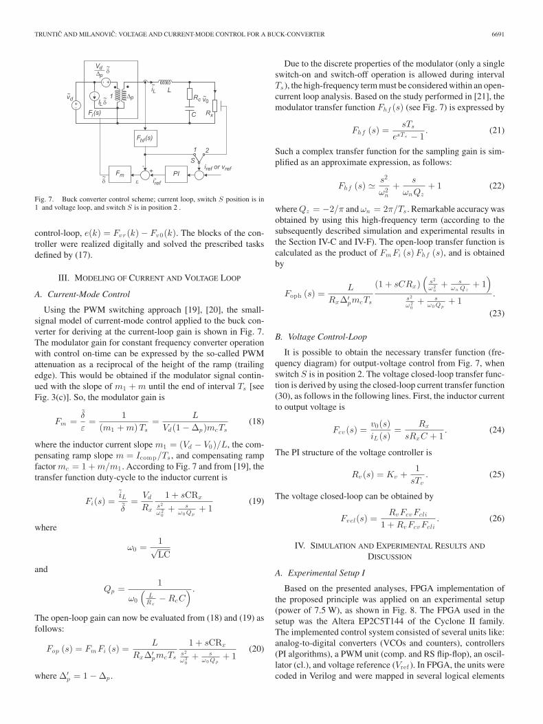
Fig. 7. Buck converter control scheme; current loop, switch S position is in1 and voltage loop, and switch S is in position 2 .
control-loop, e(k) = Fvr (k) − Fv0(k). The blocks of the con-troller were realized digitally and solved the prescribed tasksdefined by (17).
III. MODELING OF CURRENT AND VOLTAGE LOOP
A. Current-Mode Control
Using the PWM switching approach [19], [20], the small-signal model of current-mode control applied to the buck con-verter for deriving at the current-loop gain is shown in Fig. 7.The modulator gain for constant frequency converter operationwith control on-time can be expressed by the so-called PWMattenuation as a reciprocal of the height of the ramp (trailingedge). This would be obtained if the modulator signal contin-ued with the slope of m1 + m until the end of interval Ts [seeFig. 3(c)]. So, the modulator gain is
Fm =δ
ε=
1(m1 + m) Ts
=L
Vd(1 − Δp)mcTs(18)
where the inductor current slope m1 = (Vd − V0)/L, the com-pensating ramp slope m = Icomp/Ts , and compensating rampfactor mc = 1 + m/m1 . According to Fig. 7 and from [19], thetransfer function duty-cycle to the inductor current is
Fi(s) =iL
δ=
Vd
Rx
1 + sCRx
s2
ω 20
+ sω0 Qp
+ 1(19)
where
ω0 =1√LC
and
Qp =1
ω0
(L
Rx− RcC
) .
The open-loop gain can now be evaluated from (18) and (19) asfollows:
Fop (s) = Fm Fi (s) =L
RxΔ′pmcTs
1 + sCRx
s2
ω 20
+ sω0 Qp
+ 1(20)
where Δ′p = 1 − Δp .
Due to the discrete properties of the modulator (only a singleswitch-on and switch-off operation is allowed during intervalTs), the high-frequency term must be considered within an open-current loop analysis. Based on the study performed in [21], themodulator transfer function Fhf (s) (see Fig. 7) is expressed by
Fhf (s) =sTs
esTs − 1. (21)
Such a complex transfer function for the sampling gain is sim-plified as an approximate expression, as follows:
Fhf (s) � s2
ω2n
+s
ωnQz+ 1 (22)
where Qz = −2/π and ωn = 2π/Ts . Remarkable accuracy wasobtained by using this high-frequency term (according to thesubsequently described simulation and experimental results inthe Section IV-C and IV-F). The open-loop transfer function iscalculated as the product of Fm Fi (s) Fhf (s), and is obtainedby
Foph (s) =L
RxΔ′pmcTs
(1 + sCRx)(
s2
ω 2n
+ sωn Qz
+ 1)
s2
ω 20
+ sω0 Qp
+ 1.
(23)
B. Voltage Control-Loop
It is possible to obtain the necessary transfer function (fre-quency diagram) for output-voltage control from Fig. 7, whenswitch S is in position 2. The voltage closed-loop transfer func-tion is derived by using the closed-loop current transfer function(30), as follows in the following lines. First, the inductor currentto output voltage is
Fcv (s) =v0(s)iL (s)
=Rx
sRxC + 1. (24)
The PI structure of the voltage controller is
Rv (s) = Kv +1
sTv. (25)
The voltage closed-loop can be obtained by
Fvcl(s) =RvFcvFcli
1 + RvFcvFcli. (26)
IV. SIMULATION AND EXPERIMENTAL RESULTS AND
DISCUSSION
A. Experimental Setup I
Based on the presented analyses, FPGA implementation ofthe proposed principle was applied on an experimental setup(power of 7.5 W), as shown in Fig. 8. The FPGA used in thesetup was the Altera EP2C5T144 of the Cyclone II family.The implemented control system consisted of several units like:analog-to-digital converters (VCOs and counters), controllers(PI algorithms), a PWM unit (comp. and RS flip-flop), an oscil-lator (cl.), and voltage reference (Vref ). In FPGA, the units werecoded in Verilog and were mapped in several logical elements

6692 IEEE TRANSACTIONS ON POWER ELECTRONICS, VOL. 29, NO. 12, DECEMBER 2014
Fig. 8. Experimental setup I: converter with the control board.
TABLE IEXPERIMENTAL SETUP I PARAMETERS
Fig. 9. Bode diagram compensating current slope design.
that consume hardware quantity. Signal conditioning and com-ponent synchronization was also necessary in order to apply theproposed principle.
B. Current Controller Parameter Design—Setup I
1) Current Controller Design: Based on transfer functionmodeling from Section III, using (18) to (26), the current andvoltage controller were designed by using the Bode plots. Basedon the parameters indicated in Table I, the bode plot of theopen-loop transfer function calculated from (20) is shown inFig. 9 (Fop—dashed line). Using this frequency characteris-tic, the compensating ramp can be designed under the dif-ferent circumstances. It can be seen that subharmonic oscil-lations are absent because at half of the switching frequency(ωs = 7.85 × 10⁴ ⇒ fs/2 = 12.5 kHz) is only π/2 phase de-lay and the system is stable. When the high frequency termis considered, the subharmonic oscillation appears. This phe-nomena is shown in Fig. 9. It is evident that without the com-pensating ramp, the open-loop gain is at half of the switchingfrequency 1.76 dB with a phase margin at that point of ϕ = πthat causes the subharmonic oscillations. An appropriate com-pensating ramp slope (Icomp = 0.15 A) stabilizes the inductorcurrent. On the other hand, the compensating ramp causes staticerror. In order to evaluate this, it is necessary to obtain the
Fig. 10. Bode diagram of open current control loop.
closed-loop transfer function Fcli(s) = iL /i′ref , as follows:
Fcli (s) =Fm Fi(s)
1 + Fm Fi(s)Fhf (s). (27)
The static error εs can be evaluated by
iL (∞) = limt→∞
iL (t) = lims→0
sFcli (s) i′ref (s) = KDC (28)
where
KDC =1
Δ′pmc
Ts
τL
where τL = L/Rx . The static error can be finally calculatedwhen the unity step function is used for i′ref (t) as follows:
εs(∞) =i′ref (t) − iL (∞)
i′ref (t)= (1 − KDC). (29)
When the buck converter acts as a current source, the static errorcan be removed by using of PI controller (Ri(s)) in an inductorcurrent control-loop, as also shown in Fig. 7, when the switchS is in position 1 . The closed-loop transfer function referencecurrent iref to inductor current iL is obtained
FcPI (s) =iLiref
=Fm Fi(s)Ri(s)
1 + Fm Fi(s)Fhf (s)(1 + Ri(s)). (30)
The open-loop transfer function was considered in order to de-sign the controller parameters. The open-loop is derived from(30)
FopR (s) = Fm Fi(s)Fhf (s)(1 + Ri(s)). (31)
The parameters of the PI controller with a transfer function
Ri (s) = Ki +1
sTi(32)
where the design using the Bode plot is shown in Fig. 10. Byconsidering the process parameters from Table I, the gain Ki =1.5 and integrating time constant Ti = 240 μs were chosen.
2) Voltage Controller Design: The open-loop part of (26)FcvFcli is appropriate for voltage control design
Fov (s) = FcvFcli . (33)
Fig. 11 shows the frequency diagram of (33). The system seemsto be stable but can become unstable when the voltage-loop is

TRUNTIC AND MILANOVIC: VOLTAGE AND CURRENT-MODE CONTROL FOR A BUCK-CONVERTER 6693
Fig. 11. Bode diagram of open-voltage control loop.
Fig. 12. Bode diagram of closed-voltage control loop, the PI controller pa-rameters are designed.
closed. This can be seen in Fig. 12, where the Bode plot oftransfer function is shown
FoRv (s) = RvFcvFcli . (34)
The voltage-controller gain was chosen as Kv = 5 and time-constant Tv = 1.2ms with the help of the frequency diagram(see Fig. 12).
C. Simulation Results of Current-Mode Control
The current-mode operation of the described buck converterwas first investigated by simulation using MATLAB/Simulink.The buck-converter parameters are indicated in Table I. All sim-ulation results were obtained when the load resistance changedat t = 16ms from Rx = 6.8 Ω → 3.4 Ω and at t = 28ms fromRx = 3.4 Ω → 6.8 Ω.
First, simulation was performed at the operating point wherethe duty-cycle did not exceed 1/2 (Δp < 0.5), as shown inFig. 13(a). This operating point was reached by setting the ref-erence of the inductor current peak-value to iref = 0.70 A. Thesubharmonic oscillations are absent. Fig. 13(b), (c), and (d)show the cutoffs during the start-up, load-up, and load-down,respectively. At the next operating point reached by setting thereference of inductor current peak-value to iref = 1.00 A, theduty-cycle function exceeded 1/2 (Δp > 0.5), the control ofinductor-current peak-value was also reached but subharmonicoscillation was visible, as shown in Fig. 13(e). Fig. 13(f), (g),
and (h) show the cutoffs during the start-up, load-up, and load-down, respectively. During the time-interval t ∈ (16ms, 28 ms)(load-down), the duty-cycle does not exceeded 1/2 and subhar-monic oscillation is absent. The compensating ramp with theslope of m = 0.4A/Ts was designed by using the Bode plot inFig. 10. The simulation results are shown in Fig. 13(i). Fig. 13(j),(k), and (l) show the cutoffs during the start-up, load-up, andload-down, respectively. It was evident that the compensatingramp stabilized the inductor current, and subharmonic oscilla-tion disappeared but, as was expected, the static error appeared.
D. Current-Mode Control and PI Compensating Circuit
In the closed current-loop for control purposes, the only pa-rameter possible to change is the modulator gain by changingthe slope of the compensating ramp. Static error will appearin current-mode control in this regard. This undesirable behav-ior can be removed by the introduction of the PI compensator(switch S in Fig. 7 is in position 1 ). The PI controller param-eters are designed by using the Bode plot in Fig. 10. Fig. 14(a)shows the simulation results when applying the PI compensatorand Fig. 14(b), (c), and (d) show the cutoffs during the start-up,load-up, and load-down, respectively. It is evident that the staticerror had been completely removed. The buck converter worksas current source.
E. Simulation of Voltage-Control Loop
The buck-converter operation for output-voltage control wasalso verified by simulation. The control scheme shown in Fig. 7was used for this purposes, (switch S is in position 2 ). ThePI compensator parameters and appropriate compensating rampslope were designed by using the Bode plot in Fig. 11. Fig. 15(a)shows the output-voltage response and Fig. 14(b), (c), and (d)show the cutoffs during the start-up, load-up, and load-down,respectively. The DR calculation is also applied. Dynamic errorduring loads up and down was less than ±100 mV (±2%).
F. Experimental Results of Current-Mode Control
The current-mode control was investigated experimentally.All the described procedures were investigated and all attemptswere considered regarding the start-up and load changes at spe-cific time-instants. The load changed at t = 16 ms from Rx =6.8 Ω → 3.4 Ω, and at t = 28 ms from Rx = 3.4 Ω → 6.8 Ω.The DR was calculated as followed in (14). Fig. 16(a) shows theexperimental results when no compensating ramp was applied.Fig. 16(b) shows the detail during the start-up, and Fig. 16(c) and(d) show the details of the load-up and load-down, respectively.Instability appeared (subharmonic oscillation, double peaks) butthe peak of the inductor current reached the current reference.Due to subharmonic oscillation, the inductor current appearedto have lower switching frequency and, consequently, doubleripple. In order to avoid the oscillations, a compensating rampwas introduced within the control system as follows from (14)by applying the DR in current-mode control. The compensat-ing ramp was designed with the help of the frequency charac-teristic shown in Fig. 9. The inductor current response when

6694 IEEE TRANSACTIONS ON POWER ELECTRONICS, VOL. 29, NO. 12, DECEMBER 2014
Fig. 13. Simulation of current-mode control; (a) dynamic current reference response when Δp < 0.5 (without compensating ramp); (b), (c), and (d) thedetails of start-up, load changes; Rx = 6.8 Ω → 3.4 Ω, and Rx = 3.4 Ω → 6.8 Ω, respectively; (e) dynamic current reference response when Δp > 0.5 (withoutcompensating ramp); (f), (g), and (h) the details of start-up, load changes; Rx = 6.8 Ω → 3.4 Ω, and Rx = 3.4 Ω → 6.8 Ω, respectively; (i) dynamic currentreference response when Δp > 0.5 (with compensating ramp); (j), (k), and (l) the details of start-up, load changes; Rx = 6.8 Ω → 3.4 Ω, and Rx = 3.4 Ω →6.8 Ω, respectively.
Fig. 14. Simulation of current-mode control; (a) with PI compensator, dynamic current reference, and compensating ramp; (b), (c), and (d) the details of start-up,load changes, Rx = 6.8 Ω → 3.4 Ω, and Rx = 3.4 Ω → 6.8 Ω, respectively.
Fig. 15. Simulation of output-voltage control; (a) with PI compensator, dynamic current reference, and compensating ramp; (b), (c), and (d) the details of start-up,load changes; Rx = 6.8 Ω → 3.4 Ω, and Rx = 3.4 Ω → 6.8 Ω, respectively.

TRUNTIC AND MILANOVIC: VOLTAGE AND CURRENT-MODE CONTROL FOR A BUCK-CONVERTER 6695
Fig. 16. Experimental results current mode control: (a) The oscillations in current-mode control when no compensating ramp is applied; (b), (c), and (d) thedetails of start-up, load changes; Rx = 6.8 Ω → 3.4 Ω, and Rx = 3.4 Ω → 6.8 Ω, respectively. (e) The stabilized current-mode control when the compensatingramp of m = 0.4 A/Ts is applied; (f), (g), and (h) the details of start-up, load changes; Rx = 6.8 Ω → 3.4 Ω, and Rx = 3.4 Ω → 6.8 Ω, respectively. (i) Thestabilized current mode control when compensating ramp of m = 0.4 A/Ts and PI controller are applied; (j), (k), and (l) the details of start-up, load changes;Rx = 6.8 Ω → 3.4 Ω, and Rx = 3.4 Ω → 6.8 Ω, respectively; for (a), (e), and (i), x-axis 5 ms/div, voltage y-axis 1V/div, current y-axis 0.5 A/div, and all thecloseups have x-axis 200 μs/div.
Fig. 17. Experimental results of voltage control: (a) The whole sequences of voltage control during the start-up and load change x-axis 5ms/div, voltage y-axis1V/div, current y-axis 0.5A/div; (b), (c), and (d) the details of start-up, load changes; Rx = 6.8 Ω → 3.4 Ω, and Rx = 3.4 Ω → 6.8 Ω, respectively; all thecloseups have x-axis 200μs/div.
the compensating ramp was applied, is shown Fig. 16(e), withthe detailed responses during the start-up, load-up, and load-down are shown in Fig. 16(f), (g), and (h), respectively. It isobvious that subharmonic oscillation disappeared from the cur-rent response but static error appeared. The static error canbe removed from the system by introducing the PI controllerand by a new feedback loop. Fig. 10 shows the frequency di-
agram necessary for designing the PI controller gain Ki andtime-constant Ti . Fig. 16(i) shows the inductor current responsewhen the compensating ramp and PI controller were applied,and the current responses during the start-up, load-up, and load-down are shown in Fig. 16(j), (k), and (l). The current subhar-monic oscillation and static error is not presented in the currentresponse.

6696 IEEE TRANSACTIONS ON POWER ELECTRONICS, VOL. 29, NO. 12, DECEMBER 2014
Fig. 18. Experiment, the load changes; Rx = 6.8 Ω → 3.4 Ω, and Rx =3.4 Ω → 6.8 Ω, respectively: (a) voltage response, when input voltage of 10 Vis applied; (b) voltage response, when input voltage of 12 V is applied; x-axis5ms/div, voltage y-axis 1V/div, and current y-axis 0.5A/div.
Fig. 19. Experiment, the voltage transient: (a) when DR current calculationis not applied; (b) when DR current calculation is applied; x-axis 200μs/div,voltage v0 y-axis 200mV/div, voltage vd y-axis 5V/div, and current y-axis0.5A/div.
Fig. 20. Experimental setup II: (a) four-leg buck converter; (b) the controlboard; FPGA with five VCOs; (c) The half-bridge converter, IGBT with drivers,and current measurement (single converter leg).
G. Experimental Results of Voltage Control
The VCO measurement principle was also applied for output-voltage measurements, as was outlined in the previous text. Theoutput-voltage control was experimentally verified with the helpof all the described analyses. The current-mode controller wasincluded within a control-loop as a kind of modulator. The outer
Fig. 21. Four-leg buck-converter scheme.
Fig. 22. Bode diagram compensating current slope design (experimental setupII).
TABLE IIEXPERIMENTAL SETUP II; PARAMETERS
voltage-loop was controlled by using the PI controller. Basedon small signal analysis as described in Section III-B, the pa-rametersof the controller and the compensating ramp slope weredesigned in order to have responses without any kind of insta-bility. Fig. 17(a) shows the transient response when the loadresistance was changed (6.8Ω → 3.4 Ω → 6.8 Ω). The voltagereference was set at 5V . Fig. 17(b), show the start-up responseof the buck-converter output voltage and inductor current. Thepeak of the inductor current was limited to 1.75A. Fig. 17(c) and(d) show closeups at the load change from 6.8Ω → 3.4 Ω and3.4Ω → 6.8 Ω, respectively. The voltage controller generatedthe current reference which changed from 0.75 A to 1.5 A, andvice versa. The voltage dynamic error was less than ±100 mV(±2%). The compensating ramp slope of m = 0.5A/Ts assuredthe stability of the inductor current as well as the output voltage.The voltage control was also studied when the input voltage vd
changes it’s value. Fig. 18(a) and (b) shows the whole sequencewhen the load resistance changed from Rx = 6.8 Ω → 3.4 Ωand afterwards from Rx = 3.4Ω → 6.8 Ω when the input volt-age was 10 and 12 V, respectively. The only difference evidentfrom this response is inductor current ripple that was larger inthe case when the input voltage was 12 V. Fig. 19(a) and (b)

TRUNTIC AND MILANOVIC: VOLTAGE AND CURRENT-MODE CONTROL FOR A BUCK-CONVERTER 6697
Fig. 23. Experiment, the current-mode control; (a) start-up, dynamic current reference with compensating ramp response; (b) and (c) the current response whenthe load changes; Rx = 9.5 Ω → 14.6 Ω, and Rx = 14.6Ω → 9.5 Ω, respectively; (d) start-up, with PI compensator; (e) and (f) the current response when theload changes; Rx = 9.5 Ω → 14.6 Ω, and Rx = 14.6Ω;→ 9.5 Ω, respectively; x-axis 1ms/div; y-axis: v0 100 V/div, i0 , iL 1 toiL 4 5 A/div.
Fig. 24. Bode diagram for current PI-compensator parameters design.
shows the transient when input voltage Vd changes from 10 to12 V, and when DR is excluded and when it is included, respec-tively. It is evident from the transient in Fig. 19(b) that there isalmost no response in the output voltage (less than 1%).
H. Experimental Setup II
In order to verify the proposed control method, the 16-kWfour-leg dc–dc converter was designed. Fig. 20 shows the ex-perimental setup. The converter is built as bidirectional struc-ture with buck and boost operation using four half-bridges asshown scheme in Fig. 21. The proposed algorithm was mainlytested with DR on a 6-kW converter operating in buck regime,with the elements indicated in Table II. Four VCO convert-ers were used for current measurement and one for voltagemeasurement.
Fig. 25. Bode diagram for voltage PI-compensator parameters design.
I. Experimental Results
1) Current-Mode Control: The current-mode control prin-ciple with the DR and compensating ramp was applied on four-leg buck converter. In order to design the compensating rampslope, the Bode diagram was calculated as follows from (30)to (32). Fig. 22 shows frequency characteristic where compen-sating ramp of 4A/Ts stabilized the currents in each converterleg. The experimental results of current-mode controlled buckconverter are shown in Fig. 23(a), (b), and (c), where the ref-erence current was set to iref = 20A. It is evident that the usedprinciple causes the current static errors as was expected. So,the current control is performed as follows from Fig. 7, whenswitch S is in position 1 . Based on frequency diagrams shownin Fig. 24, the gain Ki = 1.5 and integrators’ time constant ofTi = 100μs are designed. The reference current was set to 20 Aand PI controller was sufficient to regulate the output current ina way that the converter acts as a current source.

6698 IEEE TRANSACTIONS ON POWER ELECTRONICS, VOL. 29, NO. 12, DECEMBER 2014
Fig. 26. Experiment, voltage-mode control; (a) start-up when PI compensator and DR is used; (b) and (c) the load changes; Rx = 9.5 Ω → 14 Ω, andRx = 14.6Ω → 9.5 Ω, respectively; x-axis 1ms/div; y-axis: v0 40 V/div, i0 , iL 1 toiL 4 5 A/div.
2) Voltage Control: The voltage control is performed as fol-lows from Fig. 7, when switch S is in position 2 . The con-verter operates in voltage-control mode. The converter oper-ates under the transient conditions when the output power re-quirement changes from 2.8 to 4.0 kW. By using the frequencycharacteristic as shown in Fig. 25, the PI-controller parametergain of Kv = 3.7 and time constant Ti = 230μs were designed.Fig. 26(a), (b), and (c) show the transients during the start-upand load-up and down for output voltage, current, and inductorcurrents. It is evident from the transient [see Fig. 26(b) and (c)]that over and under shoot in the output voltage is less than 4%.
V. CONCLUSION
This paper proposed a current-mode control algorithm suit-able for digitalization. The algorithm is based on measurementsof the inductor current and the output-voltage integrals (the areaunder the current and voltage curves). Both measurements wereperformed by using VCOs. The peak inductor current modecontrol was performed by the introduction of a current dynamicreference. Based on the analytical analysis, the measurementprinciple and the dynamic reference calculation algorithm weredeveloped and applied during the simulation and experimenta-tion. Such an approach showed that the used measurement prin-ciple is capable of rejecting the switching disturbances duringcurrent and voltage measurements, which usually appear due totransistor and diode switching operations. For control purposes,a small signal analysis was used for controller design. All thedeveloped algorithms were applied within the FPGA circuit.Such an approach is suitable for the implementation of all al-gorithms within the FPGA circuit. It is, therefore, adequate forseveral industrial applications such as high-power multiphasedc–dc converters.
REFERENCES
[1] E. Vidal-Idiarte, L. Martnez-Salamero, F. Guinjoan, J. Calvente, andS. Gomariz, “Sliding and fuzzy control of a boost converter using an8-bit microcontroller,” IEE Proc.-Electr. Power Appl., vol. 151, no. 1,pp. 5–11, Jan. 2004.
[2] M. Milanovic, M. Truntic, P. Slibar, and D. Dolinar, “Reconfigurabledigital controller for a buck converter based on FPGA,” Microelectron.Rel., vol. 47, no. 1, pp. 150–154, Jan. 2007.
[3] D. Trevisan, P. Mattavelli, and P. Tenti, “Digital control of single-inductormultiple-output step-down dc–dc converters in CCM,” IEEE Trans. Ind.Electron., vol. 55, no. 9, pp. 3476–3483, Sep. 2008.
[4] A. Simon-Muela, S. Petibon, C. Alonso, and J.-L. Chaptal, “Practicalimplementation of a high-frequency current-sense technique for VRM,”IEEE Trans. Ind. Electron., vol. 55, no. 9, pp. 3221–3230, Sep. 2008.
[5] L. Guo, J. Y. Hung, and R. M. Nelms, “Evaluation of DSP-based PIDand fuzzy controllers for dc–dc converters,” IEEE Trans. Ind. Electron.,vol. 56, no. 6, pp. 2237–2248, Jun. 2009.
[6] M. Barai, S. Sengupta, and J. Biswas, “Dual-mode multiple-band digi-tal controller for high-frequency dc–dc converter,” IEEE Trans. PowerElectron., vol. 24, no. 3, pp. 752–766, Mar. 2009.
[7] H. Matsuo, F. Kurokawa, and M. Asano, “Overcurrent limiting character-istics of the dc–dc converter with a new digital current-injected controlcircuit,” IEEE Trans. Power Electron., vol. 13, no. 4, pp. 645–650, Jul.1998.
[8] B. Bryant and M. K. Kazimierczuk, “Open-loop power-stage transferfunctions relevant to current-mode control of boost PWM converter oper-ating in CCM,” IEEE Trans. Circuits Syst. I, Reg. Papers, vol. 52, no. 10,pp. 2158–2164, Oct. 2005.
[9] F. Kurokawa and S. Sukita, “A new model control dc–dc converter toimprove dynamic characteristics,” in Proc. IEEE Power Electron. DriveSyst., 2007, pp. 763–767.
[10] F. Kurokawa and K. Kajiwara, “A new digital average current-injectedcontrol dc–dc converter using VCO,” in Proc. Int. Conf. Electr. Mach.Syst, Aug. 2011, pp. 1–5.
[11] E. Meyer, Z. Zhang, and Y.-F. Liu, “Digital charge balance controllerto improve the loading/unloading transient response of buck converters,”IEEE Trans. Power Electron., vol. 27, no. 3, pp. 1314–1326, Mar. 2012.
[12] M. J. Park, “A fourth order continuous-time ΣΔ ADC with VCO-basedintegrator and quantizer”, Ph.D. dissertation, Dept. Electr. Eng. Comput.Sci., Massachusetts Inst. Technol., Cambridge, MA, USA, Feb. 2009
[13] Y. Qiu, H. Liu, and X. Chen, “Digital average current-mode control ofPWM dc–dc converters without current sensors,” IEEE Trans. Ind. Elec-tron., vol. 57, no. 5, pp. 1670–1677, May 2010.
[14] B. J. Patella, A. Prodic, A. Zirger, and D. Maksimovic, “High-frequencydigital PWM controller IC for dc–dc converters,” IEEE Trans. PowerElectron., vol. 18, no. 1, pp. 438–446, Jan. 2003.
[15] E. Monmasson, L. Idkhajine, M. N. Cirstea, I. Bahri, A. Tisan, andM. W. Naouar, “FPGAs in industrial control applications,” IEEE Trans.Ind. Informat., vol. 7, no. 2, pp. 224–243, May 2011.
[16] M. Truntic, M. Milanovic, E. Vidal-Idiarte, C. Carrejo, and C. Alonso,“Digital current mode and voltage control for the dc–dc step-up converterbased on the FPGA technology,” in Proc. 14th Int. Power Electron. MotionControl Conf., 2010, pp. S913–S917.
[17] J. Wang and J. Xu, “Peak current mode bifrequency control technique forswitching dc–dc converters in DCM with fast transient response and lowEMI,” IEEE Trans. Power Electron., vol. 27, no. 4, pp. 1876–1884, Apr.2012.
[18] J. A. Gow and C. D. Manning, “Novel fast-acting predictive current modecontroller for power electronic converters,” IEE Proc.-Electr. Power Appl.,vol. 148, no. 2, pp. 133–139, Mar. 2001.
[19] V. Vorperian, “Simplified analysis of PWM converters using the modelof PWM switch part I: Continuous conduction mode,” Trans. Aerosp.Electron. Syst., vol. 26, no. 3, pp. 490–596, May 1990.
[20] V. Vorperian, “Simplified analysis of PWM converters using the modelof PWM switch part II: Discontinuous conduction mode,” Trans. Aerosp.Electron. Syst., vol. 26, no. 3, pp. 497–505, May 1990.
[21] R. B. Ridley, “A new small-signal model for current mode control”, Ph.D.dissertation, Bradley Dept. Electr. Comput. Eng., Virginia PolytechnicInst. State Univ., Blacksburg, VA, USA, 1990

TRUNTIC AND MILANOVIC: VOLTAGE AND CURRENT-MODE CONTROL FOR A BUCK-CONVERTER 6699
[22] M. Hovin, A. Olsen, T. Sverre, and C. Toumazou, “Delta–sigma modula-tors using frequency-modulated intermediate values,” IEEE J. Solid-StateCircuits, vol. 32, no. 1, pp. 13–22, Jan. 1997.
[23] S. R. Sanders, “On limit-cycles and the describing function-method inperiodically switched circuits,” IEEE Trans. Circuits Syst. I, Fundam.Theory Appl., vol. 40, no. 9, pp. 564–572, Sep. 1993.
[24] A. V. Peterchev and S. R. Sanders, “Quantization resolution and limitcycling in digitally controlled PWM converters,” in Proc. IEEE 32ndAnnu. Power Electron. Spec. Conf., Jun. 2001, vol. 2, pp. 465–471.
Mitja Truntic received the B.Sc. and Ph.D. degreesboth in electrical engineering from the University ofMaribor, Maribor, Slovenia, in 2004 and 2009, re-spectively.
In 2004, he joined the Institute for Robotics, FERIUniversity, Maribor, as a Ph.D. student. Currently,he is a Researcher and Designer of power convertors.His research interests include power converters, espe-cially dc–dc converters, and implementation of non-linear control algorithms for different kind of powerconverters into FPGA in/or DSP’s.
Miro Milanovic (M’87) received the B.Sc., M.Sc.,and Ph.D. degrees in electrical engineering from theUniversity of Maribor, Maribor, Slovenia, in 1978,1984, and 1987, respectively.
From 1978 to 1981, he was a Power Electron-ics Research Engineer with TSN Company, Maribor.Since 1981, he has been a Faculty Member of theFaculty of Electrical Engineering and Computer Sci-ences, University of Maribor, where he is currentlya Full Professor. In 1993, he was a Visiting Scholarat the University of Wisconsin, Madison, WI, USA,
and in 1999, he spent two months at the University of Tarragona, Tarragona,Spain, as a Visiting Professor. His main research interests include the control ofpower electronics circuits, unity power factor correction, and switching matrixconverters. He served as the Vice-President of the Slovenian IEEE section from2002 to 2006.