vlsi test basics - electrical & computer...
TRANSCRIPT

HOST VLSI Test Basics ECE 495/595
1 (2/4/13)
Big Picture
Customer’s needs
Determine requirements
Write specifications
Design synthesis and verification
Test development
Fabrication
Test
Chips to customers

HOST VLSI Test Basics ECE 495/595
2 (2/4/13)
Design Verification vs. Manufacturing Test
• Design Verification: Predictive analysis to ensure that the synthesized
design, when manufactured, will perform the given I/O function
• Test: A process that ensures that the physical device, manufactured from
the synthesized design, has no manufacturing defects
Verification Test
* Verifies correctness of design.* Performed by simulation, hardware
emulation or formal methods.
* Performed "once" prior to manufacturing.
* Verifies correctness of hardware.* Two-parts:
Test generation: software processexecuted "once" during design.Test application: electrical testsapplied to hardware.
* Test application performed onEVERY manufactured device.

HOST VLSI Test Basics ECE 495/595
3 (2/4/13)
Ideal vs Real TestsIdeal tests detect all defects produced in a manufacturing process
Pass all functionally good chips, fail all defective chips
Very large numbers and varieties of possible defects need to be tested
Difficult to generate tests for some real defects -- defect-based testing is an
active research area
Universe of DefectsFaultmodel
A
Faultmodel
B
Fault modelC
Faultsdetectedby test set
fault coverage
Ideal tests candetect all defectsin this universe

HOST VLSI Test Basics ECE 495/595
4 (2/4/13)
Ideal vs Real TestsFault models may not map onto real defects
A fault is a logic level abstraction of a physical defect that is used to
describe the change in the logic function of a device caused by the
defect.
It is difficult to generate tests that detect every possible fault in the chip due
to high design complexity
Some good chips are rejected
The fraction of such chips is called yield loss
Some bad chips are shipped
The fraction of bad chips among all passing chips is called defect level
(test escapes)
Benefits of Testing:
Quality and economy: Quality means satisfying the user’s need at a min-
imum cost

HOST VLSI Test Basics ECE 495/595
5 (2/4/13)
Roles of TestingDetection: Go/no-go, is the chip manufactured properly?
Diagnosis: A process to determine where, in the IC, the failure is occurring.
Performed on chips that fail go/no-go tests
Failure Analysis (FA): A process to determine the specific manufacturing pro-
cess steps that are producing the defects
Performance Characterization: For speed binning parts
Process characterization: A process designed to help with yield learning
Design for Manufacturability: A process for establishing which design rules
and guidelines are best to improve an IC’s yield
Trust and Security?: Will test "get stuck with" hardware security and trust

HOST VLSI Test Basics ECE 495/595
6 (2/4/13)
Components of TestDesign for Testability (DFT): On-chip components added to make test easier
Scan-chains
BIST
Software processes associated with test:
Automatic test pattern generation (ATPG)
Fault simulation
Automatic test equipment (ATE) programming and debug
Manufacturing test:
Application of test vectors by ATE
Input patterns
ChipPIs or
Scan inputs
POs or
Scan outputs
--11--01--00
Output responses
--11--01--00
Stored responses
Comparator--11--01--00

HOST VLSI Test Basics ECE 495/595
7 (2/4/13)
ATE for Manufacturing Test
HOST VLSI Test Basics ECE 495/595
8 (2/4/13)
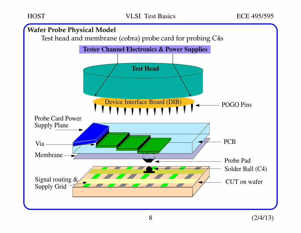
Wafer Probe Physical ModelTest head and membrane (cobra) probe card for probing C4s
Device Interface Board (DIB)
Tester Channel Electronics & Power Supplies
Test Head
Probe Card PowerSupply Plane
Via PCB
Probe Pad
Solder Ball (C4)
Membrane
POGO Pins
CUT on waferSignal routing &Supply Grid

HOST VLSI Test Basics ECE 495/595
9 (2/4/13)
Cantilever Style Probe Cards

HOST VLSI Test Basics ECE 495/595
10 (2/4/13)
Test ProgrammingThe test program and test vectors are needed once the chip is contacted
CAD tools are used to automate the generation of the test programs
Chip specifications Logic designTest generation
Physical design
(from simulators)
test plan
TestProgramGenerator
vectors
test types
timing specspin assignments
Test program

HOST VLSI Test Basics ECE 495/595
11 (2/4/13)
4 Basic Types of TestingCharacterization testing, design debug or verification testing:
Verifies correctness of design and test procedure
Production (go/no-go test):
Factory testing of all manufactured chips for parametric faults and for
random defects
Shorter and less intensive test performed on every chip
Main driver is cost -- test time MUST be minimized
But tests must have high coverage of faults to ensure high quality
Burn-in or stress test:
Testing designed to stress the chip and accelerate the mechanisms that
cause the chip to fail
Acceptance testing or incoming inspection:
Customer performs tests on purchased parts to ensure quality

HOST VLSI Test Basics ECE 495/595
12 (2/4/13)
Test Flow
Masks
In-line Wafer Tests
Wafer Sort
DC Parametrics
Manufacturing
Functional
IDDQ Delay
Burn-In
Packaged Device
Fallout
Fallout
Package Test
System Test
System Integration
Die
GO/
Logic
Customer Incominginspection
Customer
no-GO Testescapes
Testescapes

HOST VLSI Test Basics ECE 495/595
13 (2/4/13)
Physical DefectsDefects can be caused by dust particles on the mask, wafer surface or process-
ing chemicals, e.g. photoresist
During photolithography, these particles lead to unexposed photoresist
areas, leading to:
• Unwanted material or unwanted etching of the material
• Causes shorts and opens in the poly, active or metal layers
Opens in CMOS circuits are more difficult to detect because fault behavior is
dependent on location, resistance and values of parasitic coupling cap, leak-
age currents, etc.

HOST VLSI Test Basics ECE 495/595
14 (2/4/13)
Single stuck-at faults (SSF)Assumes defects cause the signal net or line to remain at a fixed voltage level
Model includes stuck-at-0 (SA0) or stuck-at-1 (SA1) faults and assumes
only one fault exists
For example, how many SSF faults can occur on an n-input NAND gate?
What fault(s) does the pattern AB = 01 detect?
What is the minimum number of tests needed to "detect" all of them?
A B
Z
Inputs Fault-Free Faulty Response
AB Response A/0 B/0 Z/0 A/1 B/1 Z/100 1 1 1 0 1 1 101 1 1 1 0 0 1 110 1 1 1 0 1 0 111 0 1 1 0 0 0 1

HOST VLSI Test Basics ECE 495/595
15 (2/4/13)
Single stuck-at faults (SSF)An n-line circuit can have at most 2n SSF faults.
This number can be further reduced through fault collapsing.
Fault detection requires:
• A test t activates or provokes the fault f.
• t propagates the error to observation point (primary output (PO)/scan latch).
A line that changes with f is said to be sensitized to the fault site.
Fault propagation requires off-path inputs be set to non-dominant values.
AND1
AND2
OR
1
1
0
0SA1
1
0(1)0(1)
True responseFaulty response
14 faults possible here.
01, 10, and 11do not provokethe fault

HOST VLSI Test Basics ECE 495/595
16 (2/4/13)
Delay Faults
Delays along every path from PI to PO or between internal latches must be
less than the operational system clock interval
An SA0 or SA1 can be modeled as a delay fault in which the signal takes an
infinite amount of time to change to 1 or 0, respectively
Passing stuck fault tests is usually not sufficient however for systems
that operate at any appreciable speed
Test Definition:
• At time t1, the initializing vector of the two-pattern test, V1, is applied
through the input latches or PIs and the circuit is allowed to stabilize
• At time t2, the second test pattern, V2, is applied
• At time t3, a logic value measurement (a sample) is made at the output
latches or POs
The delay test vectors V1 and V2 may sensitize one or more paths, pi

HOST VLSI Test Basics ECE 495/595
17 (2/4/13)
Delay Tests
Let:
• TC = (t3 - t2) represent the time interval between the application of vector V2
at the PIs and the sampling event at the POs
• The nominal delay of each of these paths be defined as pdi
• The slack of each path be defined as sdi = TC - pdi
This is the difference between the propagation delay of each of the sensi-
tized paths in the nominal circuit and the test interval
CombinationalLogic
From FFs or PIs
To FFs or POs
Clock period
Transient region
Delay of combination logiccannot exceed the clock period
Slack
t2 t3

HOST VLSI Test Basics ECE 495/595
18 (2/4/13)
Delay Fault Test Generation
Difficulties with delay fault test generation:
• Test generation requires a sensitized path that extends from a PI to a PO
• Path selection heuristics must be used because the total number of paths is
exponentially related to the number of inputs and gates in the circuit
• The application of the test set must be performed at the rated speed of the
device
This requires test equipment that is capable of accurately timing two-
vector test sequences
• The detection of a defect that introduces an additional delay, adi, along a sen-
sitized path is dependent on satisfying the condition:
adi > sdi (or pdi + adi > TC)

HOST VLSI Test Basics ECE 495/595
19 (2/4/13)
Delay Tests
The critical path(s) of this circuit is 6 time units
Let’s set the clock period T = 7
Assume only one faulty path
No delay fault is detected if path delay along P3 is less than 7 units
A
B
C
2 4 6
1 3
2 5
2
1
3
1
e g
qh
j K
P1: A-h-KP2: B-e-q-h-KP3: B-e-g-j-K

HOST VLSI Test Basics ECE 495/595
20 (2/4/13)
ScanScan proposed in ’73 by Williams and Angell
Main idea is to obtain control and observability for FFs
It reduces sequential TPG to combinational TPG
With Scan, a synchronous sequential circuit works in two modes
Normal mode and test mode:
In test mode, all FFs are configured as a shift register, with Scan-in and
Scan-out routed to a (possibly dedicated) PI and PO
Combo logic
FFs
PIs POs
Combo logic
FFs
PIs POs
Scan-in Scan-out

HOST VLSI Test Basics ECE 495/595
21 (2/4/13)
Storage Cells for Scan DesignsAn implementation using two-port master-slave FF with a MUX
To ensure race-free operation, use a 2-phase nonoverlapping clk
φ
D
D Q
Qφ
L1
2-to-1 MUX
SISel
D Q
Qφ
L2Q1 Q2
φ1
D
D Q
Qφ
L1
SISel
D Q
Qφ
L2Q1 Q2
φ2

HOST VLSI Test Basics ECE 495/595
22 (2/4/13)
Delay Test Methodologies
Launch-on-shift (LOS): Scan in of V1 is followed by one extra cycle of slow
clock with the circuit still in scan mode (TC = 0)
The test is designed so that V2 is obtained from V1 by a 1 bit translation (PI
bits of both vectors are unrestricted)
As soon as V2 is applied, mode is changed from scan to normal and Clk
is controlled at the rated period to latch outputs
Combinationalcircuit
PIs POs
SFF
SFF
Scan out
Scan inClk TC (Test Control)
Broad-side delay test or LOC
LOS
V2 by scanshift
V2
derived
Alternatively
functionallynormal mode
scan mode
scan mode
HOST VLSI Test Basics ECE 495/595
23 (2/4/13)
Delay Test Methodologies
Normal-scan sequential test
Launch-on-capture (LOC), the state portion (FF values) of V2 are function-
ally generated by the combo logic under V1
Simultaneous application of V2 at the PIs and into the FFs via Clk in nor-
mal mode generates the V1 -> V2 transitions
The outputs are latched one rated clock period later
Disadvantages:
For LOS, scan-enable must switch at rated speed of clk
For LOC, correlations between V1 and V2 may not allow high fault cov-
erage