vl6180x explorer expansion board with nucleo-f401re ... -...
TRANSCRIPT
August 2014 DocID026604 Rev 1 1/39
39
UM1796User manual
VL6180X explorer expansion board with NUCLEO-F401RE board
Introduction
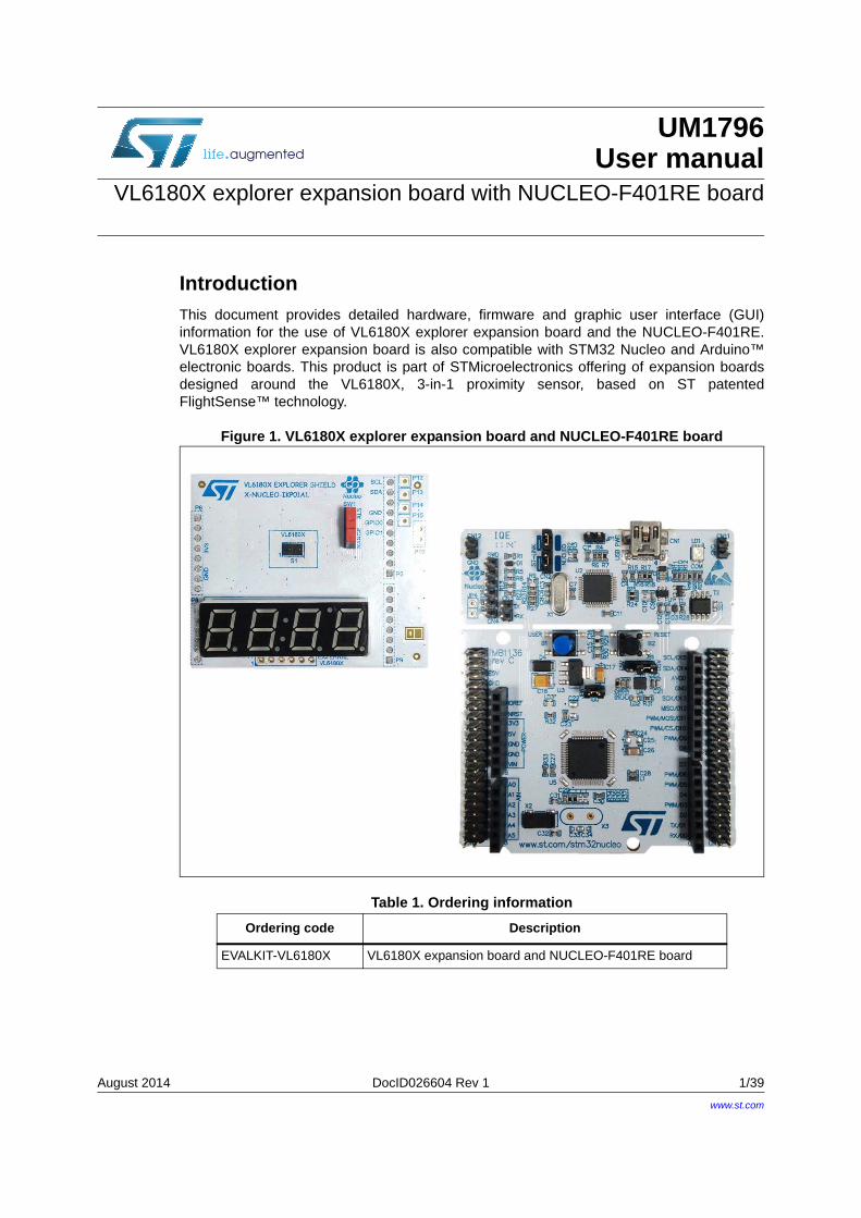
This document provides detailed hardware, firmware and graphic user interface (GUI)information for the use of VL6180X explorer expansion board and the NUCLEO-F401RE.VL6180X explorer expansion board is also compatible with STM32 Nucleo and Arduino™electronic boards. This product is part of STMicroelectronics offering of expansion boardsdesigned around the VL6180X, 3-in-1 proximity sensor, based on ST patentedFlightSense™ technology.
Figure 1. VL6180X explorer expansion board and NUCLEO-F401RE board
Table 1. Ordering information
Ordering code Description
EVALKIT-VL6180X VL6180X expansion board and NUCLEO-F401RE board
www.st.com
Contents UM1796
2/39 DocID026604 Rev 1
Contents
1 Getting started . . . . . . . . . . . . . . . . . . . . . . . . . . . . . . . . . . . . . . . . . . . . . . 4
1.1 Document references . . . . . . . . . . . . . . . . . . . . . . . . . . . . . . . . . . . . . . . . . 4
1.2 Hardware requirements . . . . . . . . . . . . . . . . . . . . . . . . . . . . . . . . . . . . . . . 4
1.3 Starting VL6180X explorer expansion board and NUCLEO-F401RE . . . . 5
1.3.1 Software requirements . . . . . . . . . . . . . . . . . . . . . . . . . . . . . . . . . . . . . . . 5
1.3.2 Getting started . . . . . . . . . . . . . . . . . . . . . . . . . . . . . . . . . . . . . . . . . . . . . 5
2 VL6180X explorer software user interface . . . . . . . . . . . . . . . . . . . . . . 11
2.1 Ranging . . . . . . . . . . . . . . . . . . . . . . . . . . . . . . . . . . . . . . . . . . . . . . . . . . .11
2.1.1 Signal strength (power) graph . . . . . . . . . . . . . . . . . . . . . . . . . . . . . . . . 12
2.1.2 Actual distance (ToF) graph . . . . . . . . . . . . . . . . . . . . . . . . . . . . . . . . . . 13
2.1.3 Actual distance (ToF) graph showing thresholds . . . . . . . . . . . . . . . . . . 15
2.2 Ambient light sensor (ALS) . . . . . . . . . . . . . . . . . . . . . . . . . . . . . . . . . . . . 15
2.3 Options . . . . . . . . . . . . . . . . . . . . . . . . . . . . . . . . . . . . . . . . . . . . . . . . . . . 18
2.3.1 Recording Data Logs . . . . . . . . . . . . . . . . . . . . . . . . . . . . . . . . . . . . . . . 18
2.3.2 Recording I2C transactions . . . . . . . . . . . . . . . . . . . . . . . . . . . . . . . . . . 18
2.4 Help . . . . . . . . . . . . . . . . . . . . . . . . . . . . . . . . . . . . . . . . . . . . . . . . . . . . . 19
2.5 Data log file . . . . . . . . . . . . . . . . . . . . . . . . . . . . . . . . . . . . . . . . . . . . . . . 20
2.6 I2C log file . . . . . . . . . . . . . . . . . . . . . . . . . . . . . . . . . . . . . . . . . . . . . . . . . 22
2.7 Range offset calibration procedure . . . . . . . . . . . . . . . . . . . . . . . . . . . . . 23
3 VL6180X explorer NUCLEO-F401RE software . . . . . . . . . . . . . . . . . . . 25
3.1 Installing updated application software to the NUCLEO-F401RE board . 25
3.2 Modifying NUCLEO-F401RE VL6180X explorer expansion board Software 25
3.3 Importing existing code into a new mbed project . . . . . . . . . . . . . . . . . . . 26
3.4 Building a project within mbed . . . . . . . . . . . . . . . . . . . . . . . . . . . . . . . . . 26
3.5 Exporting to an offline compiler . . . . . . . . . . . . . . . . . . . . . . . . . . . . . . . . 27
3.6 The VL6180X API . . . . . . . . . . . . . . . . . . . . . . . . . . . . . . . . . . . . . . . . . . 27
4 Hardware description . . . . . . . . . . . . . . . . . . . . . . . . . . . . . . . . . . . . . . . 28
4.1 VL6180X explorer expansion board . . . . . . . . . . . . . . . . . . . . . . . . . . . . . 28
4.2 Electrical schematics and list of material . . . . . . . . . . . . . . . . . . . . . . . . . 30
DocID026604 Rev 1 3/39
UM1796 Contents
39
5 Safety . . . . . . . . . . . . . . . . . . . . . . . . . . . . . . . . . . . . . . . . . . . . . . . . . . . . 37
5.1 Electrostatic precaution . . . . . . . . . . . . . . . . . . . . . . . . . . . . . . . . . . . . . . 37
5.2 Laser considerations . . . . . . . . . . . . . . . . . . . . . . . . . . . . . . . . . . . . . . . . 37
6 Revision history . . . . . . . . . . . . . . . . . . . . . . . . . . . . . . . . . . . . . . . . . . . 38
Getting started UM1796
4/39 DocID026604 Rev 1
1 Getting started
1.1 Document references
1.2 Hardware requirements
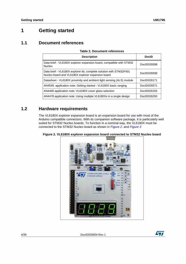
The VL6180X explorer expansion board is an expansion board for use with most of the Arduino compatible connectors. With its companion software package, it is particularly well suited for STM32 Nucleo boards. To function in a nominal way, the VL6180X must be connected to the STM32 Nucleo board as shown in Figure 2. and Figure 3
Figure 2. VL6180X explorer expansion board connected to STM32 Nucleo board
Table 2. Document references
Description DocID
Data brief - VL6180X explorer expansion board, compatible with STM32 Nucleo
DocID026598
Data brief - VL6180X explorer kit, complete solution with STM32F401 Nucleo board and VL6180X explorer expansion board
DocID026599
Datasheet - VL6180X proximity and ambient light sensing (ALS) module DocID026171
AN4545: application note: Getting started - VL6180X basic ranging DocID026571
AN4466 application note: VL6180X cover glass selection DocID026155
AN4478 application note: Using multiple VL6180Xs in a single design DocID026250
DocID026604 Rev 1 5/39
UM1796 Getting started
39
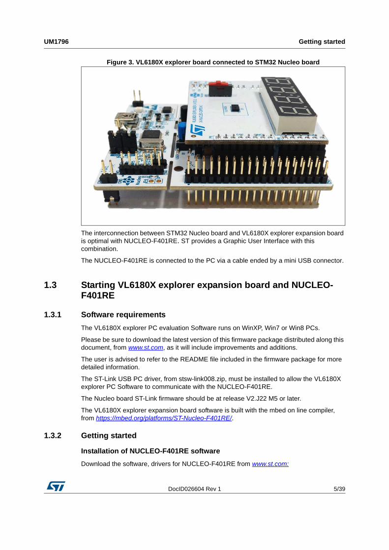
Figure 3. VL6180X explorer board connected to STM32 Nucleo board
The interconnection between STM32 Nucleo board and VL6180X explorer expansion board is optimal with NUCLEO-F401RE. ST provides a Graphic User Interface with this combination.
The NUCLEO-F401RE is connected to the PC via a cable ended by a mini USB connector.
1.3 Starting VL6180X explorer expansion board and NUCLEO-F401RE
1.3.1 Software requirements
The VL6180X explorer PC evaluation Software runs on WinXP, Win7 or Win8 PCs.
Please be sure to download the latest version of this firmware package distributed along this document, from www.st.com, as it will include improvements and additions.
The user is advised to refer to the README file included in the firmware package for more detailed information.
The ST-Link USB PC driver, from stsw-link008.zip, must be installed to allow the VL6180X explorer PC Software to communicate with the NUCLEO-F401RE.
The Nucleo board ST-Link firmware should be at release V2.J22 M5 or later.
The VL6180X explorer expansion board software is built with the mbed on line compiler, from https://mbed.org/platforms/ST-Nucleo-F401RE/.
1.3.2 Getting started
Installation of NUCLEO-F401RE software
Download the software, drivers for NUCLEO-F401RE from www.st.com:
Getting started UM1796
6/39 DocID026604 Rev 1
Note: It is not necessary to plug the VL6180X explorer expansion board on the NUCLEO-F401RE board
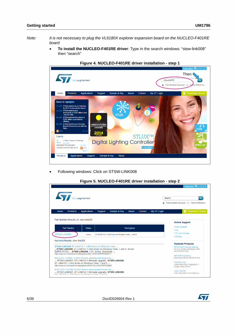
• To install the NUCLEO-F401RE driver: Type in the search windows: “stsw-link008” then “search”
Figure 4. NUCLEO-F401RE driver installation - step 1
• Following windows: Click on STSW-LINK008
Figure 5. NUCLEO-F401RE driver installation - step 2
Then
DocID026604 Rev 1 7/39
UM1796 Getting started
39
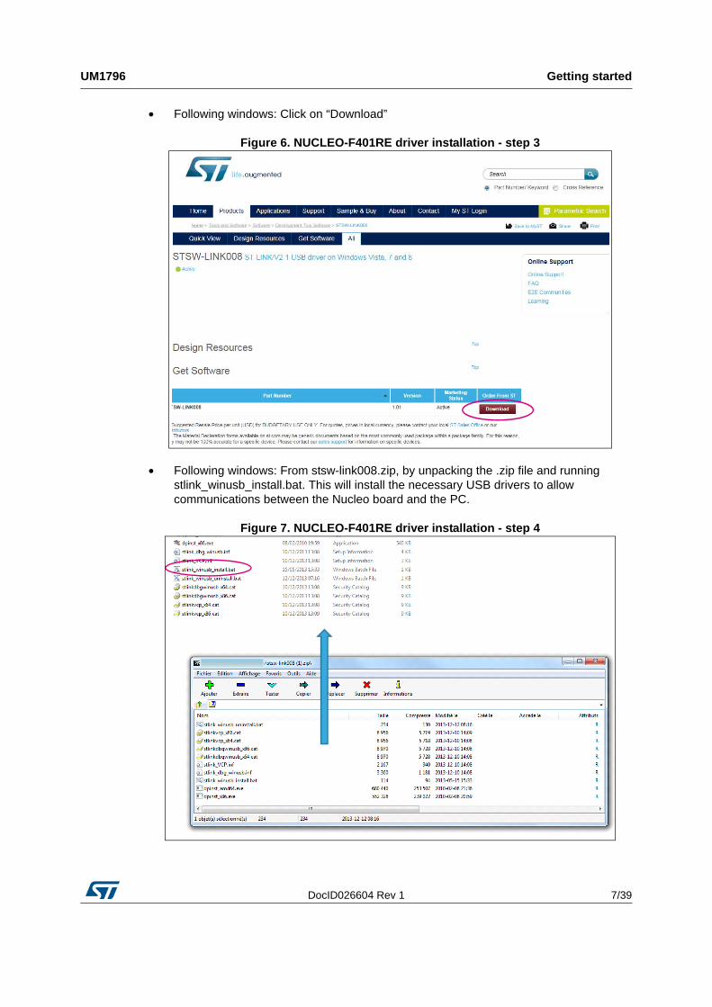
• Following windows: Click on “Download”
Figure 6. NUCLEO-F401RE driver installation - step 3
• Following windows: From stsw-link008.zip, by unpacking the .zip file and running stlink_winusb_install.bat. This will install the necessary USB drivers to allow communications between the Nucleo board and the PC.
Figure 7. NUCLEO-F401RE driver installation - step 4
Getting started UM1796
8/39 DocID026604 Rev 1
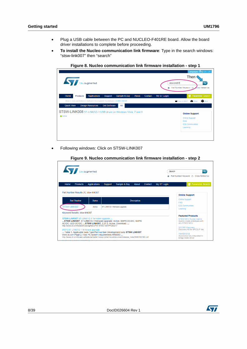
• Plug a USB cable between the PC and NUCLEO-F401RE board. Allow the board driver installations to complete before proceeding.
• To install the Nucleo communication link firmware: Type in the search windows: “stsw-link007” then “search”
Figure 8. Nucleo communication link firmware installation - step 1
• Following windows: Click on STSW-LINK007
Figure 9. Nucleo communication link firmware installation - step 2
Then
DocID026604 Rev 1 9/39
UM1796 Getting started
39
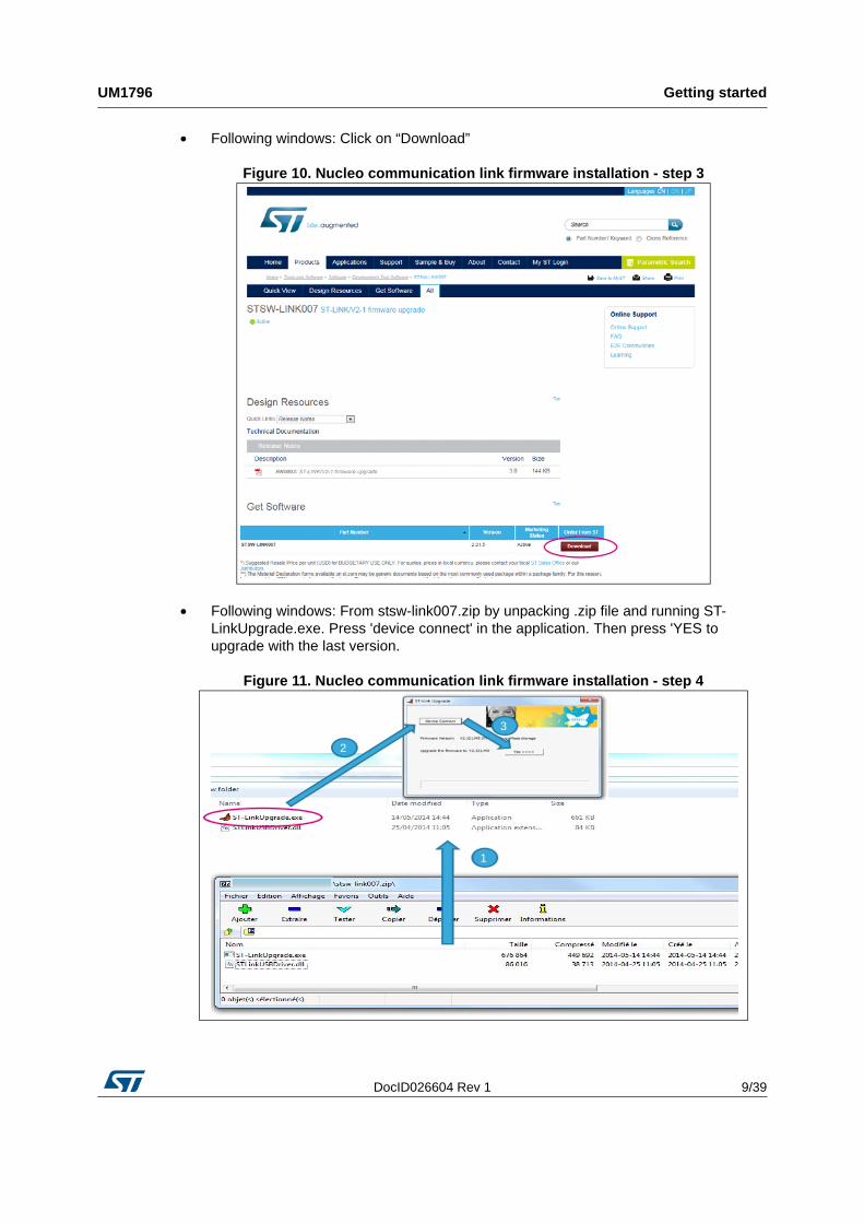
• Following windows: Click on “Download”
Figure 10. Nucleo communication link firmware installation - step 3
• Following windows: From stsw-link007.zip by unpacking .zip file and running ST-LinkUpgrade.exe. Press 'device connect' in the application. Then press 'YES to upgrade with the last version.
Figure 11. Nucleo communication link firmware installation - step 4
1
2
3
Getting started UM1796
10/39 DocID026604 Rev 1
Installation of the explorer software
To install VL6180X evaluation board software to range and ambient light value to be displayed. Please contact your local ST representative who will send the VL6180X explorer evaluation board user interface software files.
Note: If not previously plugged, plug VL6180X explorer expansion board
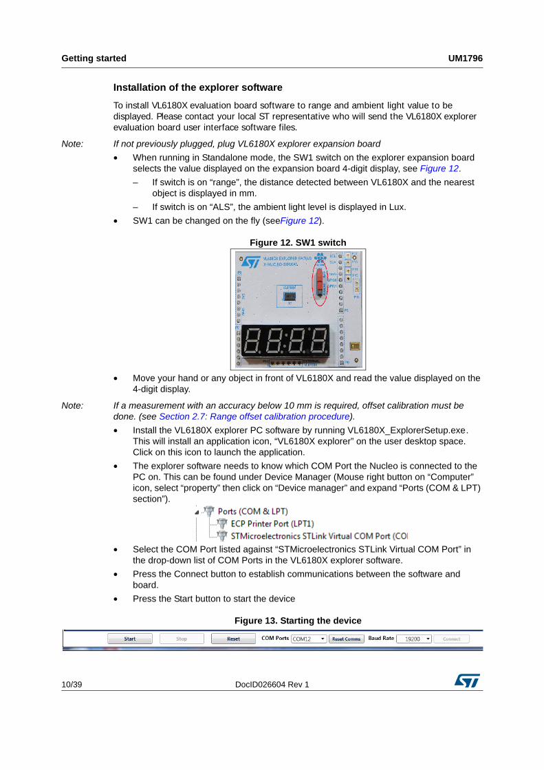
• When running in Standalone mode, the SW1 switch on the explorer expansion board selects the value displayed on the expansion board 4-digit display, see Figure 12.
– If switch is on “range”, the distance detected between VL6180X and the nearest object is displayed in mm.
– If switch is on “ALS”, the ambient light level is displayed in Lux.
• SW1 can be changed on the fly (seeFigure 12).
Figure 12. SW1 switch
• Move your hand or any object in front of VL6180X and read the value displayed on the 4-digit display.
Note: If a measurement with an accuracy below 10 mm is required, offset calibration must be done. (see Section 2.7: Range offset calibration procedure).
• Install the VL6180X explorer PC software by running VL6180X_ExplorerSetup.exe-. This will install an application icon, “VL6180X explorer” on the user desktop space. Click on this icon to launch the application.
• The explorer software needs to know which COM Port the Nucleo is connected to the PC on. This can be found under Device Manager (Mouse right button on “Computer” icon, select “property” then click on “Device manager” and expand “Ports (COM & LPT) section”).
• Select the COM Port listed against “STMicroelectronics STLink Virtual COM Port” in the drop-down list of COM Ports in the VL6180X explorer software.
• Press the Connect button to establish communications between the software and board.
• Press the Start button to start the device
Figure 13. Starting the device
DocID026604 Rev 1 11/39
UM1796 VL6180X explorer software user interface
39
2 VL6180X explorer software user interface
The VL6180X explorer software contains several tabs that can be used to display, calibrate and configure various features of the VL6180X. The available tabs are:
• Ranging, see Section 2.1
• ALS, see Section 2.2
• Options, see Section 2.3
• Help, see Section 2.4
2.1 Ranging
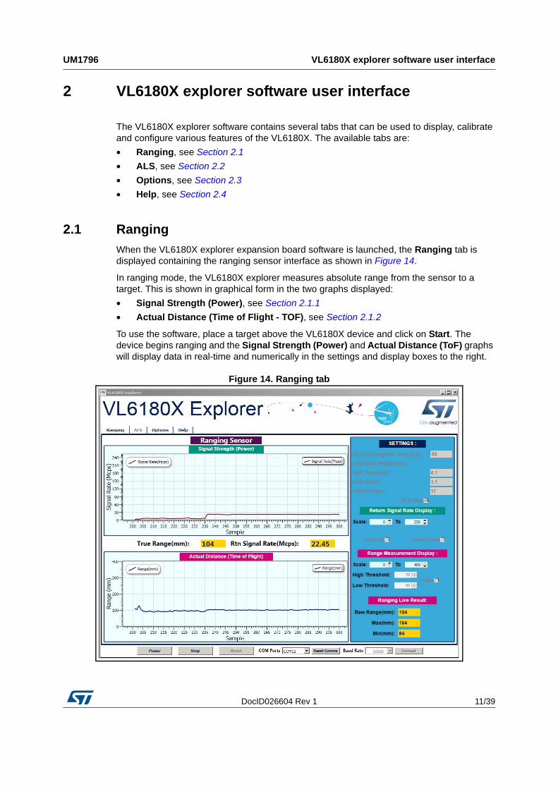
When the VL6180X explorer expansion board software is launched, the Ranging tab is displayed containing the ranging sensor interface as shown in Figure 14.
In ranging mode, the VL6180X explorer measures absolute range from the sensor to a target. This is shown in graphical form in the two graphs displayed:
• Signal Strength (Power), see Section 2.1.1
• Actual Distance (Time of Flight - TOF), see Section 2.1.2
To use the software, place a target above the VL6180X device and click on Start. The device begins ranging and the Signal Strength (Power) and Actual Distance (ToF) graphs will display data in real-time and numerically in the settings and display boxes to the right.
Figure 14. Ranging tab
VL6180X explorer software user interface UM1796
12/39 DocID026604 Rev 1
The buttons listed in Table 3 are available at the bottom of the Ranging tab.
2.1.1 Signal strength (power) graph
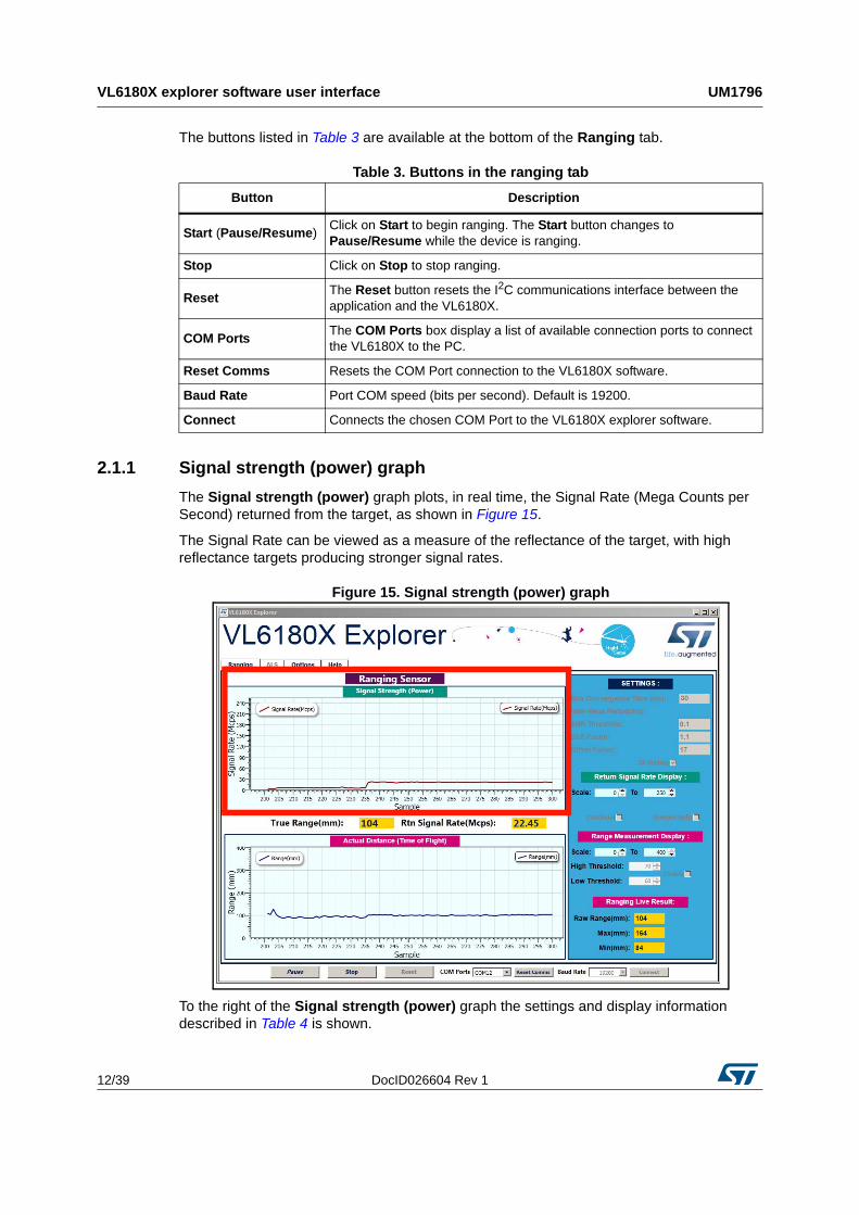
The Signal strength (power) graph plots, in real time, the Signal Rate (Mega Counts per Second) returned from the target, as shown in Figure 15.
The Signal Rate can be viewed as a measure of the reflectance of the target, with high reflectance targets producing stronger signal rates.
Figure 15. Signal strength (power) graph
To the right of the Signal strength (power) graph the settings and display information described in Table 4 is shown.
Table 3. Buttons in the ranging tab
Button Description
Start (Pause/Resume)Click on Start to begin ranging. The Start button changes to Pause/Resume while the device is ranging.
Stop Click on Stop to stop ranging.
Reset The Reset button resets the I2C communications interface between the application and the VL6180X.
COM PortsThe COM Ports box display a list of available connection ports to connect the VL6180X to the PC.
Reset Comms Resets the COM Port connection to the VL6180X software.
Baud Rate Port COM speed (bits per second). Default is 19200.
Connect Connects the chosen COM Port to the VL6180X explorer software.
DocID026604 Rev 1 13/39
UM1796 VL6180X explorer software user interface
39
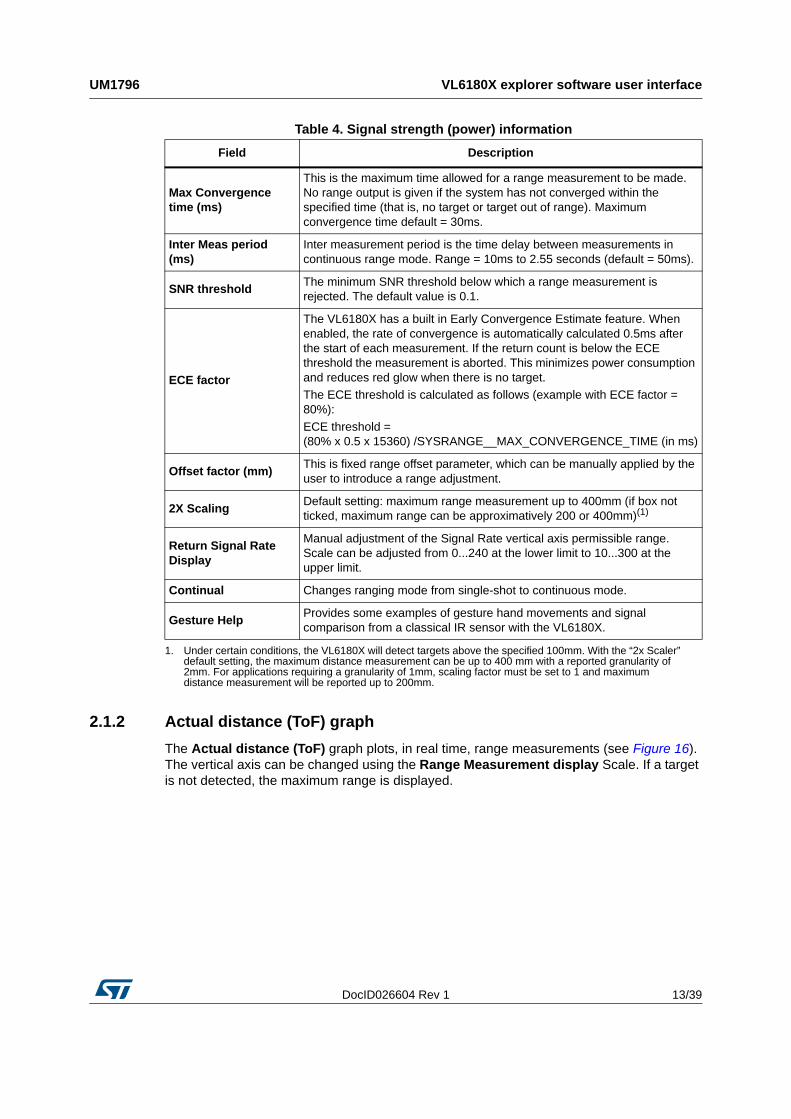
2.1.2 Actual distance (ToF) graph
The Actual distance (ToF) graph plots, in real time, range measurements (see Figure 16). The vertical axis can be changed using the Range Measurement display Scale. If a target is not detected, the maximum range is displayed.
Table 4. Signal strength (power) information
Field Description
Max Convergence time (ms)
This is the maximum time allowed for a range measurement to be made. No range output is given if the system has not converged within the specified time (that is, no target or target out of range). Maximum convergence time default = 30ms.
Inter Meas period (ms)
Inter measurement period is the time delay between measurements in continuous range mode. Range = 10ms to 2.55 seconds (default = 50ms).
SNR threshold The minimum SNR threshold below which a range measurement is rejected. The default value is 0.1.
ECE factor
The VL6180X has a built in Early Convergence Estimate feature. When enabled, the rate of convergence is automatically calculated 0.5ms after the start of each measurement. If the return count is below the ECE threshold the measurement is aborted. This minimizes power consumption and reduces red glow when there is no target.
The ECE threshold is calculated as follows (example with ECE factor = 80%):
ECE threshold = (80% x 0.5 x 15360) /SYSRANGE__MAX_CONVERGENCE_TIME (in ms)
Offset factor (mm)This is fixed range offset parameter, which can be manually applied by the user to introduce a range adjustment.
2X ScalingDefault setting: maximum range measurement up to 400mm (if box not ticked, maximum range can be approximatively 200 or 400mm)(1)
1. Under certain conditions, the VL6180X will detect targets above the specified 100mm. With the “2x Scaler” default setting, the maximum distance measurement can be up to 400 mm with a reported granularity of 2mm. For applications requiring a granularity of 1mm, scaling factor must be set to 1 and maximum distance measurement will be reported up to 200mm.
Return Signal Rate Display
Manual adjustment of the Signal Rate vertical axis permissible range. Scale can be adjusted from 0...240 at the lower limit to 10...300 at the upper limit.
Continual Changes ranging mode from single-shot to continuous mode.
Gesture Help Provides some examples of gesture hand movements and signal comparison from a classical IR sensor with the VL6180X.
VL6180X explorer software user interface UM1796
14/39 DocID026604 Rev 1
Figure 16. Actual distance (ToF) graph
The VL6180X explorer can be run in single-shot ranging mode (default) or continuous ranging mode (by ticking the Continual check box to the right of the Signal Strength (Power) graph, see Figure 15). If in Continual ranging mode the time between measurements can be changed by adjusting the Inter-Meas Period (ms).
The Actual Distance (ToF) graph can be changed to show threshold information, see Section 2.1.3.
To the right of and above the Actual Distance (ToF) graph, the information described in Table 5 is displayed.
Table 5. Actual distance (ToF) information
Field Description
Actual Distance (ToF) Display
Manual adjustment of the Range vertical axis permissable range. Scale can be adjusted from 0...110 at the lower limit to 10...255 at the upper limit.
Enable Check the Enable box to allow thresholding to be enabled.
Low Threshold Manual adjustment of the lower threshold limit (default is 60mm).
When enabled, this threshold line is shown in the Actual Distance (ToF) graph. See Actual distance (ToF) graph showing thresholds.
High Threshold Manual adjustment of the upper threshold limit (default is 70mm).
When enabled, this threshold line is shown in the Actual Distance (ToF) graph. See Actual distance (ToF) graph showing thresholds.
Raw Range (mm) This is the range measurement including the Offset Factor.
Max & Min (mm) These are post-processed measurement statistics to make noise evaluation easier to characterize. The max and min are the range data measured by the sensor over 100 measured sample points.
DocID026604 Rev 1 15/39
UM1796 VL6180X explorer software user interface
39
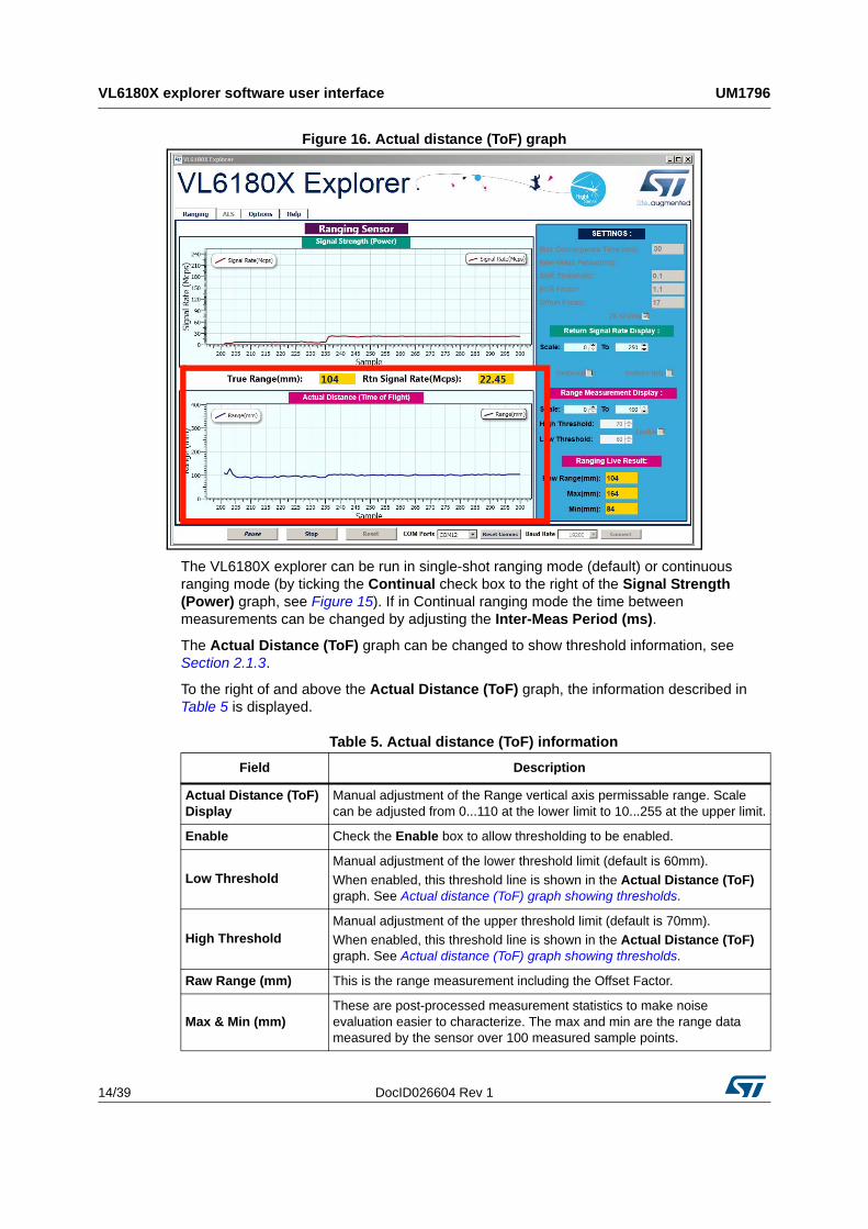
2.1.3 Actual distance (ToF) graph showing thresholds
The thresholding feature allows the user to define upper and lower limits and be alerted as the range measurements transition across these limits by the display changing color. Figure 17 shows examples of the Actual Distance (ToF) graph with high and low thresholding enabled. It shows a minimum threshold of 60 mm, a maximum threshold of 150 mm and range measurements above and below the thresholds.
If the range measurement goes below the lower threshold the graph turns green as shown in the top graph. If it goes above the upper threshold the graph turns pink as shown in the lower graph. The graph will stay pink/green, till the lower/upper threshold is crossed.
Thresholding is enabled by checking the Enable check box (see Table 5) and the upper and lower threshold settings can be modified in the High & Low Threshold settings.
Figure 17. Actual distance graphs showing high and low thresholds
2.2 Ambient light sensor (ALS)
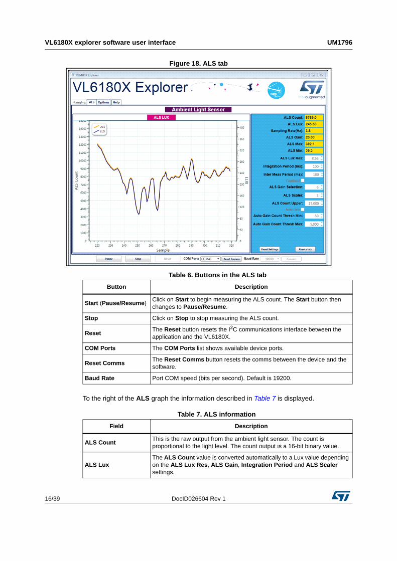
The ambient light sensor can be activated in the ALS tab. This tab displays the ALS Count graph showing ALS Lux/count versus Samples, as shown in Figure 18. Table 6 lists the buttons available in the ALS tab.
Low threshold reached: with green background display
High threshold reached: with red background display
VL6180X explorer software user interface UM1796
16/39 DocID026604 Rev 1
Figure 18. ALS tab
To the right of the ALS graph the information described in Table 7 is displayed.
Table 6. Buttons in the ALS tab
Button Description
Start (Pause/Resume)Click on Start to begin measuring the ALS count. The Start button then changes to Pause/Resume.
Stop Click on Stop to stop measuring the ALS count.
Reset The Reset button resets the I2C communications interface between the application and the VL6180X.
COM Ports The COM Ports list shows available device ports.
Reset Comms The Reset Comms button resets the comms between the device and the software.
Baud Rate Port COM speed (bits per second). Default is 19200.
Table 7. ALS information
Field Description
ALS Count This is the raw output from the ambient light sensor. The count is proportional to the light level. The count output is a 16-bit binary value.
ALS Lux The ALS Count value is converted automatically to a Lux value depending on the ALS Lux Res, ALS Gain, Integration Period and ALS Scaler settings.
DocID026604 Rev 1 17/39
UM1796 VL6180X explorer software user interface
39
Sampling Rate (Hz) The number of ALS samples measured per second (PC dependent).
ALS Gain Displays the actual gain value applied corresponding to the ALS Gain Selection setting.
ALS Max &Min These are post-processed measurement statistics to make noise evaluation easier to characterize. The max, min and mean are the ALS data measured by the sensor over 100 sample points.
ALS Lux Res This calibrates the ALS Lux/count conversion. The characterized ALS Lux Res is 0.32 (default).
Integration Period (ms)
The integration period is the time range, during a single ALS measurement, over which Lux data is captured and averaged. The default integration period is 100 ms.
Inter Meas Period (ms)
The inter-measurement period is the time between each ALS measurement in continuous ALS mode. The default inter-measurement period is 10 ms.
Continual Changes ALS mode from single-shot to continuous mode.
ALS Gain Selection
This is the device register setting 0 to 7. The corresponding gain value is displayed in the ALS Gain box. Gain settings are as follows:
0: ALS Gain = 1
1: ALS Gain = 1.25
2: ALS Gain = 1.67
3: ALS Gain = 2.5
4: ALS Gain = 5
5: ALS Gain = 10
6: ALS Gain = 20
7: ALS Gain = 40
ALS Scaler
The count output is a 16-bit value. Internally, the device uses a 20-bit counter. Gain and integration time are normally used to increase sensitivity. However, if this is not sufficient and more resolution is required in low light, the ALS scaler can be used to access the 4 LSBs of the internal counter. Apply a value in the range 2 to 15 to apply additional gain.
ALS Count Upper This is the maximum scale value for the vertical axis. The default value is 15000. The user can input a new value to scale the ALS Count graph up or down as required for measurements, up to a maximum value of 65,000.
Auto Gain
Enables and disables the auto-gain feature. Auto-gain automatically adjusts the gain selection in response to the current ALS Count value in order to provide and effective dynamic range for the current lighting conditions.
Auto Gain Count Thresh Min
The manual Auto Gain ALS count threshold minimum value in Auto Gain mode.
Auto Gain Count Thresh Max
The manual Auto Gain ALS count threshold maximum value in Auto Gain mode.
Table 7. ALS information (continued)
Field Description
VL6180X explorer software user interface UM1796
18/39 DocID026604 Rev 1
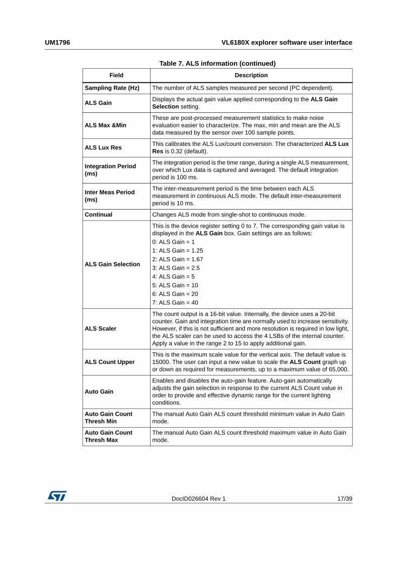
2.3 Options
The Options tab is used to enable I2C logging or data logging during ranging and ALS modes.
2.3.1 Recording Data Logs
For every measurement, relevant system data is stored in a comma separated value file (.csv) identified by date and time.
To enable data logging, in the Options tab, check the Enable Data Log box, see Figure 19.
Data logging should be selected either prior to starting measurements or during the paused state.
Figure 19. Enable data logging
Data log files are created with unique filenames and stored in: C...\Users\username\AppData\Local\STMicroElectronics\VL6180XEVK\DataLog\. See 2.5: Data log file for an example.
Before you can switch off data logging, the device must first stop ranging or ALS measurements. To do this, click on the Stop button in the Ranging tab, see Section 2.1: Ranging.
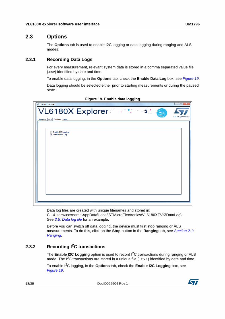
2.3.2 Recording I2C transactions
The Enable I2C Logging option is used to record I2C transactions during ranging or ALS mode. The I2C transactions are stored in a unique file (.txt) identified by date and time.
To enable I2C logging, in the Options tab, check the Enable I2C Logging box, see Figure 19.
DocID026604 Rev 1 19/39
UM1796 VL6180X explorer software user interface
39
I2C log files are stored in: C...\Users\username\AppData\Local\STMicroElectronics\VL6180XEVK\I2C\. See 2.6: I2C log file for an example.
Before you can switch off I2C logging, the device must first stop ranging or ALS measurements. To do this, click on the Stop button in the Ranging tab, see Section 2.1.
Figure 20. Enable I2C logging
2.4 Help
The Help tab provides links to documents and on line resources which provide details on the setup and functionalities of the VL6180X explorer and also details on the software version:
• HELP: To access help index
• HW User Manual: To access hardware user manual
• SW User Manual: To access software user manual
• www.ST.com/VL6180X: To access ST VL6180X product and support page
• About GUI Version: Provides the GUI version installed
VL6180X explorer software user interface UM1796
20/39 DocID026604 Rev 1
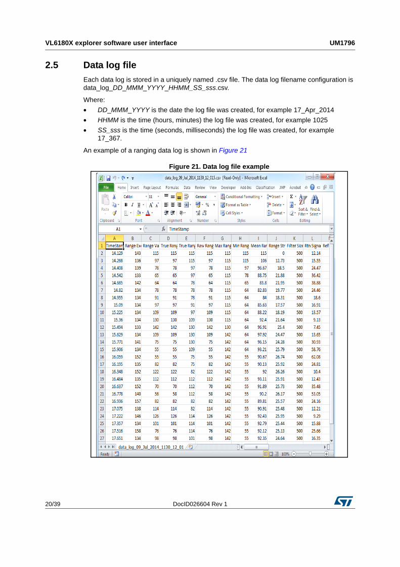
2.5 Data log file
Each data log is stored in a uniquely named .csv file. The data log filename configuration is data_log_DD_MMM_YYYY_HHMM_SS_sss.csv.
Where:
• DD_MMM_YYYY is the date the log file was created, for example 17_Apr_2014
• HHMM is the time (hours, minutes) the log file was created, for example 1025
• SS_sss is the time (seconds, milliseconds) the log file was created, for example 17_367.
An example of a ranging data log is shown in Figure 21
Figure 21. Data log file example
DocID026604 Rev 1 21/39
UM1796 VL6180X explorer software user interface
39
Range output column data definitions
A: TimeStamp: The time stamp is generated by the EVK software so the data can easily be plotted on a graph, and it represents the time of start of the test. There is latency, due to the USB interface, to send and receive data to the sensor.
B: Range Execution Time (ms): The range execution time is measured by the software for the amount of time that the test was executed to the time the data was received over the USB interface to display the data.
C: Range Val: The range value read directly from RESULT__RANGE_VAL (0x0062) in the VL6180X part on the EVK. This value includes the crosstalk compensation.
D: True Range: The range value read directly from the VL6180X part on the EVK. There is no difference between this value and the Range Value.
E: True Range Smoothed: The Raw Range value read from RESULT__RANGE_RAW (0x0064) on the VL6180X that would show a range measured without any stray light compensation.
F to I: Max, Min, Mean, Standard Deviation: Statistical data on the range data in mm gathered since the EVK software was started or the statistics were reset. Stopping and starting the capture will create a new file, but not reset the statistics.
J: Rtn Signal Rate: The actual count rate of signal returns of light measured by the return sensor when the laser is active on the return array. This is calculated by the formula:
This data is read directly from the VL6180X. Note: There are two photon triggering arrays. The first reference array is the reference array to measure the time photons have left the laser and the second return array is the array used to measure the time that the photons traveled to the target and back to the sensor.
K: Ref Signal Rate: The actual count rate of signal returns of light measured by the reference sensor when the laser is active. This is calculated by the formula:
L: Rtn Signal Count: This is the amount of sensor counts triggered by the return array on the VL6180X when the laser is active. This data is read directly from the VL6180X.
RESULT__RANGE_RETURN_SIGNAL_COUNT (0x006C)RESULT__RANGE_RETURN_CONV_TIME (0x007C)
------------------------------------------------------------------------------------------------------------------------------------------------------------
RESULT__RANGE_REFERENCE_SIGNAL_COUNT (0x0070)RESULT__RANGE_REFERENCE_CONV_TIME (0x0080)
-----------------------------------------------------------------------------------------------------------------------------------------------------------------------
VL6180X explorer software user interface UM1796
22/39 DocID026604 Rev 1
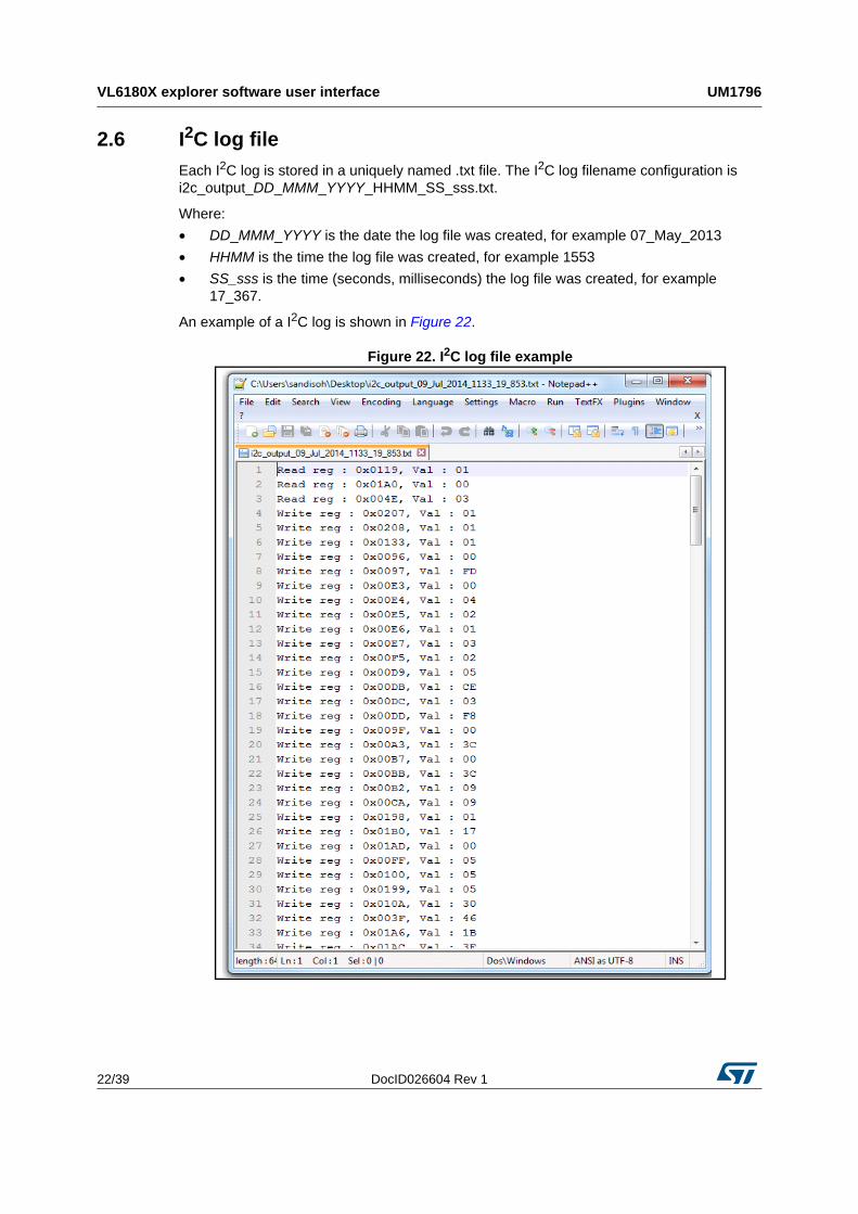
2.6 I2C log file
Each I2C log is stored in a uniquely named .txt file. The I2C log filename configuration is i2c_output_DD_MMM_YYYY_HHMM_SS_sss.txt.
Where:
• DD_MMM_YYYY is the date the log file was created, for example 07_May_2013
• HHMM is the time the log file was created, for example 1553
• SS_sss is the time (seconds, milliseconds) the log file was created, for example 17_367.
An example of a I2C log is shown in Figure 22.
Figure 22. I2C log file example
DocID026604 Rev 1 23/39
UM1796 VL6180X explorer software user interface
39
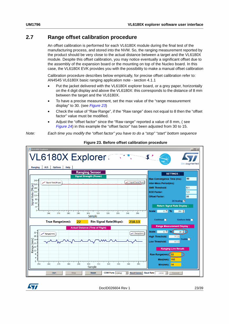
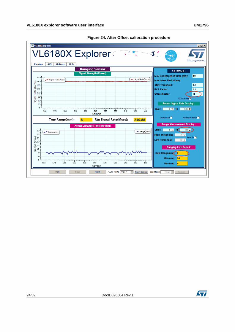
2.7 Range offset calibration procedure
An offset calibration is performed for each VL6180X module during the final test of the manufacturing process, and stored into the NVM. So, the ranging measurement reported by the product should be very close to the actual distance between a target and the VL6180X module. Despite this offset calibration, you may notice eventually a significant offset due to the assembly of the expansion board or the mounting on top of the Nucleo board. In this case, the VL6180X EVK provides you with the possibility to make a manual offset calibration
Calibration procedure describes below empirically, for precise offset calibration refer to: AN4545 VL6180X basic ranging application note - section 4.1.1
• Put the jacket delivered with the VL6180X explorer board, or a grey paper, horizontally on the 4 digit display and above the VL6180X: this corresponds to the distance of 8 mm between the target and the VL6180X.
• To have a precise measurement, set the max value of the “range measurement display” to 30. (see Figure 23)
• Check the value of “Raw Range”, if the “Raw range” does not equal to 8 then the “offset factor” value must be modified.
• Adjust the “offset factor” since the “Raw range” reported a value of 8 mm, ( see Figure 24) in this example the “offset factor” has been adjusted from 30 to 15.
Note: Each time you modify the “offset factor” you have to do a “stop” “start” bottom sequence
Figure 23. Before offset calibration procedure
VL6180X explorer software user interface UM1796
24/39 DocID026604 Rev 1
Figure 24. After Offset calibration procedure
DocID026604 Rev 1 25/39
UM1796 VL6180X explorer NUCLEO-F401RE software
39
3 VL6180X explorer NUCLEO-F401RE software
3.1 Installing updated application software to the NUCLEO-F401RE board
When connected via the USB (CN1) connector to a PC, the Nucleo board will mount as a disk-drive. New NUCLEO-F401RE application software binaries, .bin files, can be dragged or copied onto this drive root folder to be installed and automatically run.
3.2 Modifying NUCLEO-F401RE VL6180X explorer expansion board Software
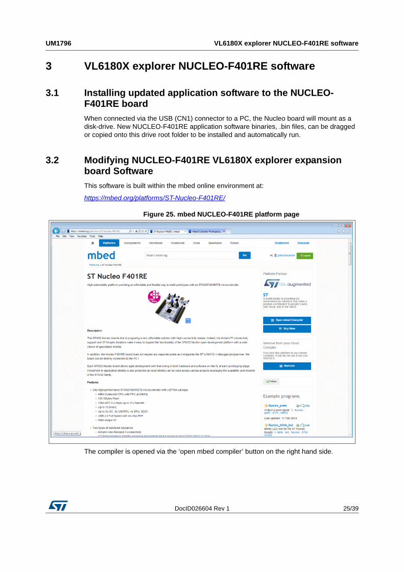
This software is built within the mbed online environment at:
https://mbed.org/platforms/ST-Nucleo-F401RE/
Figure 25. mbed NUCLEO-F401RE platform page
The compiler is opened via the ‘open mbed compiler’ button on the right hand side.
VL6180X explorer NUCLEO-F401RE software UM1796
26/39 DocID026604 Rev 1
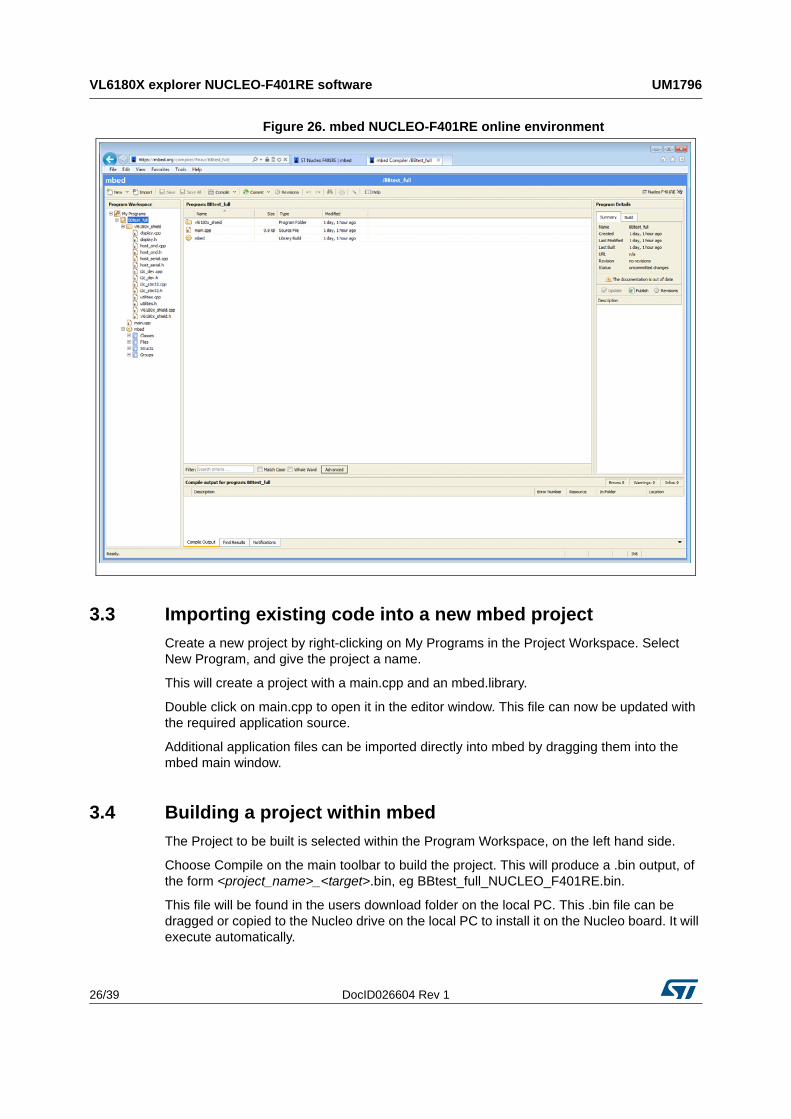
Figure 26. mbed NUCLEO-F401RE online environment
3.3 Importing existing code into a new mbed project
Create a new project by right-clicking on My Programs in the Project Workspace. Select New Program, and give the project a name.
This will create a project with a main.cpp and an mbed.library.
Double click on main.cpp to open it in the editor window. This file can now be updated with the required application source.
Additional application files can be imported directly into mbed by dragging them into the mbed main window.
3.4 Building a project within mbed
The Project to be built is selected within the Program Workspace, on the left hand side.
Choose Compile on the main toolbar to build the project. This will produce a .bin output, of the form <project_name>_<target>.bin, eg BBtest_full_NUCLEO_F401RE.bin.
This file will be found in the users download folder on the local PC. This .bin file can be dragged or copied to the Nucleo drive on the local PC to install it on the Nucleo board. It will execute automatically.
DocID026604 Rev 1 27/39
UM1796 VL6180X explorer NUCLEO-F401RE software
39
3.5 Exporting to an offline compiler
The NUCLEO-F401RE mbed environment does not allow access to any on-chip debugging facilities. However, it does support exporting the project to an offline tool which does support debugging, such as Keil, IAR, GCC or CooCox. These tools provide debug support via the Nucleo board’s in-built ST-Link JTAG port.
Exporting can be done by right-clicking on the project name within the project workspace panel and choosing Export Program.
3.6 The VL6180X API
The VL6180X application programming interface (API) is included in the VL6180X explorer expansion board sample mbed embedded software project to manage range and ALS measurements from the VL6180X device. Full API documentation and further sample uses are described in the .docs folder within the zip archive of the project. These documents can be entered from the index.html file, in any internet browser.
Hardware description UM1796
28/39 DocID026604 Rev 1
4 Hardware description
This section describes the VL6180X explorer expansion board features and provides information which could be useful for understanding the electrical schematics.
4.1 VL6180X explorer expansion board
The board allows the user to test the functionality of the VL6180X, to discover how simple it is to program and to help understanding how to develop an application using VL6180X. It is composed of:
• a 4-Digit display to render either the Range value in mm either the Ambient Light value in Lux
• a switch to select the value type to be displayed
• a 2.8V regulator to supply the VL6180X
• two level shifters to adapt the I/O level to the micro controller main board
• the necessary connectivity for the application.
It is fundamental to program a micro-controller to control the VL6180X through the I2C bus and drive the 4-digit display on board. A firmware for NUCLEO-F401RE and an example of C-ANSI source code are available on www.st.com/VL6180X.
The VL6180X explorer expansion board and STM32 Nucleo are connected through Arduino compatible connectors CN5, CN6, CN8 and CN9 as described in Table 8 and Table 9.
The Arduino connectors on STM32 Nucleo board support Arduino Uno Revision 3.
Table 8. Arduino left connector on NUCLEO-F401RE board
CN NbVL6180X
boardPin Nb Pin name MCU pin
VL6180X expansion board function
CN6 Power
- 1 NC - -
VIO 2 IOREF - Level shifter reference (3.3V)
- 3 RESET NRST -
Power 4 +3V3 - 3.3V supply
- 5 +5V - -
Gnd 6 Gnd Gnd Gnd
Gnd 7 Gnd Gnd Gnd
- 8 VIN - -
DocID026604 Rev 1 29/39
UM1796 Hardware description
39
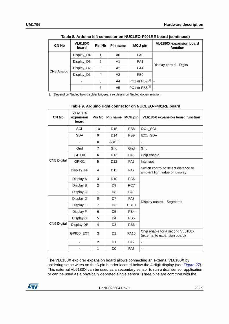
The VL6180X explorer expansion board allows connecting an external VL6180X by soldering some wires on the 6-pin header located below the 4-digit display (see Figure 27). This external VL6180X can be used as a secondary sensor to run a dual sensor application or can be used as a physically deported single sensor. Three pins are common with the
CN8 Analog
Display_D4 1 A0 PA0
Display control - DigitsDisplay_D3 2 A1 PA1
Display_D2 3 A2 PA4
Display_D1 4 A3 PB0
- 5 A4 PC1 or PB9(1) -
- 6 A5 PC1 or PB8(1) -
1. Depend on Nucleo board solder bridges, see details on Nucleo documentation
Table 9. Arduino right connector on NUCLEO-F401RE board
CN NbVL6180X
expansion board
Pin Nb Pin name MCU pin VL6180X expansion board function
CN5 Digital
SCL 10 D15 PB8 I2C1_SCL
SDA 9 D14 PB9 I2C1_SDA
- 8 AREF - -
Gnd 7 Gnd Gnd Gnd
GPIO0 6 D13 PA5 Chip enable
GPIO1 5 D12 PA6 Interrupt
Display_sel 4 D11 PA7Switch control to select distance or ambient light value on display
Display A 3 D10 PB6
Display control - Segments
Display B 2 D9 PC7
Display C 1 D8 PA9
CN9 Digital
Display D 8 D7 PA8
Display E 7 D6 PB10
Display F 6 D5 PB4
Display G 5 D4 PB5
Display DP 4 D3 PB3
GPIO0_EXT 3 D2 PA10Chip enable for a second VL6180X (external to expansion board)
- 2 D1 PA2 -
- 1 D0 PA3 -
Table 8. Arduino left connector on NUCLEO-F401RE board (continued)
CN NbVL6180X
boardPin Nb Pin name MCU pin
VL6180X expansion board function
Hardware description UM1796
30/39 DocID026604 Rev 1
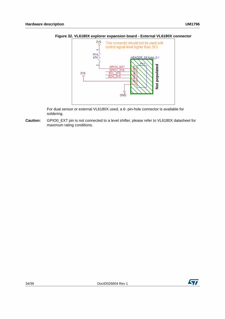
VL6180X on-board: I2C bus and GPIO1 (Interrupt) pins. GPIO0 are separate pins to control each sensor separately. Be aware the I/O named GPIO0_EXT for external VL6180X, connected to the micro-controller board is not connected to a level shifter. Refer to Figure 31 and Figure 32 for detailed connectivity.
Figure 27. Connections for external VL6180X
Note: The setting of a second VL6180X is not available on current user interface software, it will be embedded in the next release.
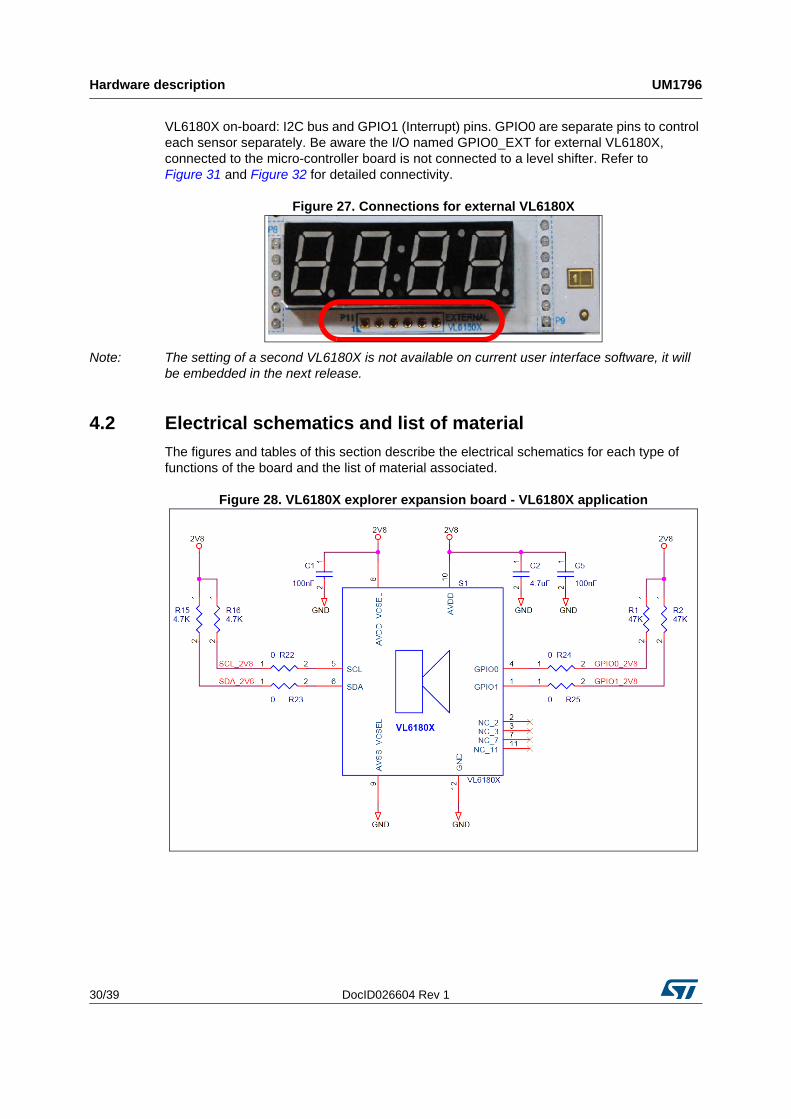
4.2 Electrical schematics and list of material
The figures and tables of this section describe the electrical schematics for each type of functions of the board and the list of material associated.
Figure 28. VL6180X explorer expansion board - VL6180X application
DocID026604 Rev 1 31/39
UM1796 Hardware description
39
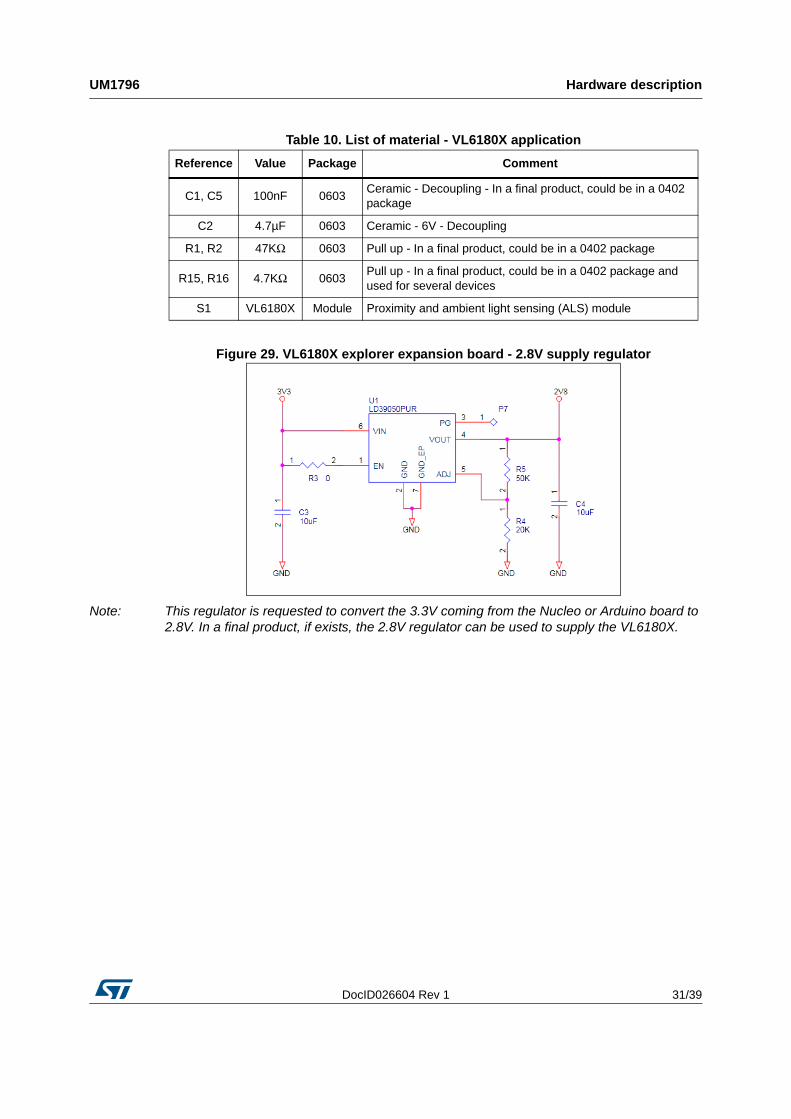
Figure 29. VL6180X explorer expansion board - 2.8V supply regulator
Note: This regulator is requested to convert the 3.3V coming from the Nucleo or Arduino board to 2.8V. In a final product, if exists, the 2.8V regulator can be used to supply the VL6180X.
Table 10. List of material - VL6180X application
Reference Value Package Comment
C1, C5 100nF 0603Ceramic - Decoupling - In a final product, could be in a 0402 package
C2 4.7µF 0603 Ceramic - 6V - Decoupling
R1, R2 47KΩ 0603 Pull up - In a final product, could be in a 0402 package
R15, R16 4.7KΩ 0603Pull up - In a final product, could be in a 0402 package and used for several devices
S1 VL6180X Module Proximity and ambient light sensing (ALS) module
Hardware description UM1796
32/39 DocID026604 Rev 1
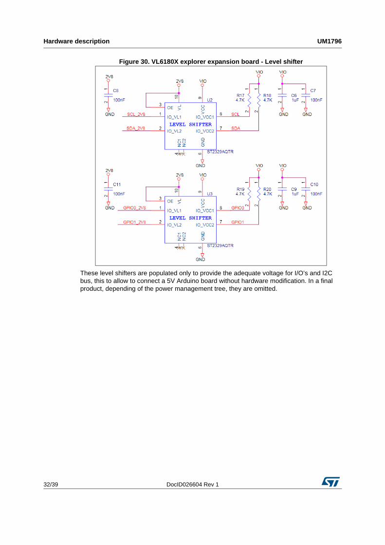
Figure 30. VL6180X explorer expansion board - Level shifter
These level shifters are populated only to provide the adequate voltage for I/O’s and I2C bus, this to allow to connect a 5V Arduino board without hardware modification. In a final product, depending of the power management tree, they are omitted.
DocID026604 Rev 1 33/39
UM1796 Hardware description
39
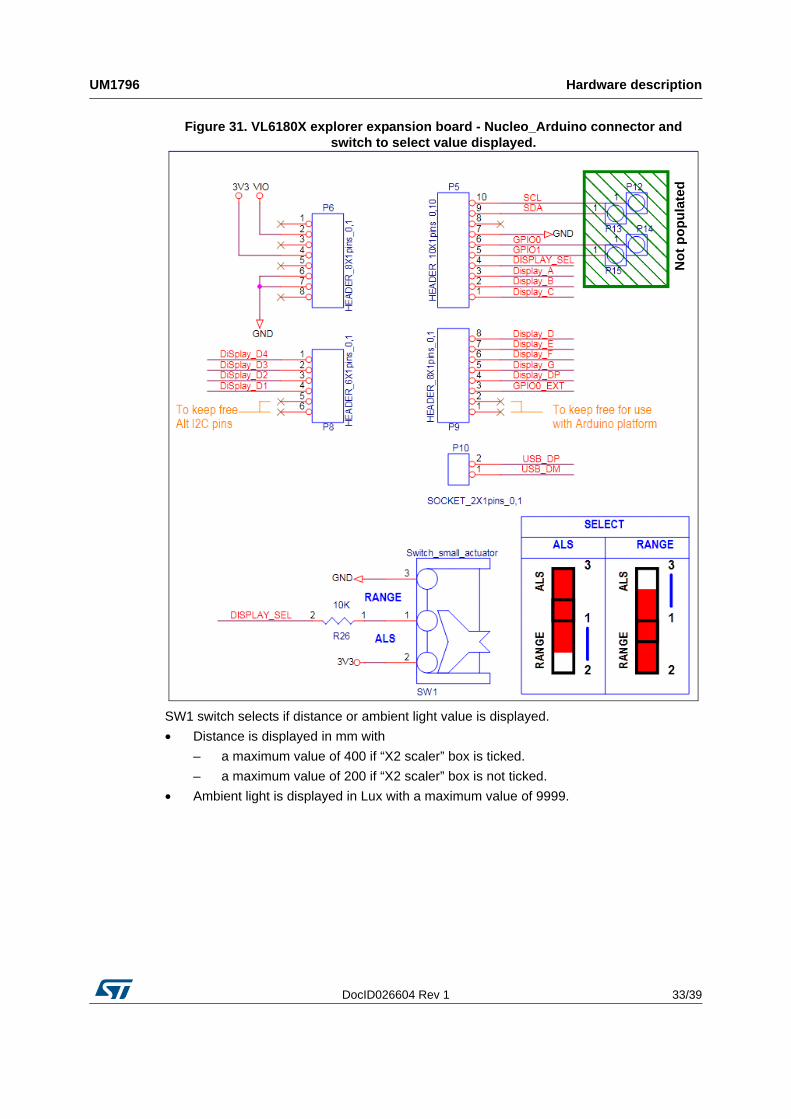
Figure 31. VL6180X explorer expansion board - Nucleo_Arduino connector and switch to select value displayed.
SW1 switch selects if distance or ambient light value is displayed.
• Distance is displayed in mm with
– a maximum value of 400 if “X2 scaler” box is ticked.
– a maximum value of 200 if “X2 scaler” box is not ticked.
• Ambient light is displayed in Lux with a maximum value of 9999.
No
t p
op
ula
ted
Hardware description UM1796
34/39 DocID026604 Rev 1
Figure 32. VL6180X explorer expansion board - External VL6180X connector
For dual sensor or external VL6180X used, a 6- pin-hole connector is available for soldering.
Caution: GPIO0_EXT pin is not connected to a level shifter, please refer to VL6180X datasheet for maximum rating conditions.
No
t p
op
ula
ted
DocID026604 Rev 1 35/39
UM1796 Hardware description
39
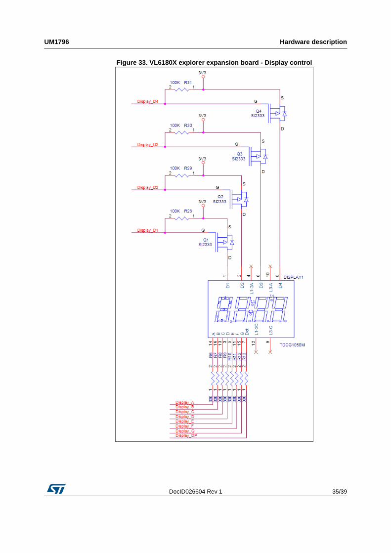
Figure 33. VL6180X explorer expansion board - Display control
Hardware description UM1796
36/39 DocID026604 Rev 1
Table 11. List of material - Other features
Reference Value Package Comment
2v8 regulator
C3, C4 10 µF 0805
R4 20 kΩ 0603
R5 50 kΩ 0603
U1 LD39050PUR DFN6 Regulator
Level shifters
C6, C9 1 µF 0603
C7, C8, C10, C11 100 nF 0603
R17, R18, R19, R20 4.7 kΩ 0603
U2, U3 ST2329AQTR QFN10 Level shifter
External VL6180X and Nucleo_Arduino connectors
R14 47 kΩ 0603
R26 10 kΩ 0603
Display control
R6, R7, R8, R9, R10, R11, R12, R13
300 Ω 0603
R28, R29, R30, R31 100 kΩ 0603
Q1, Q2, Q3, Q4 SI2333 SOT23 P channel MOSFET
Display1 TDCG1050M 4 digits
DocID026604 Rev 1 37/39
UM1796 Safety
39
5 Safety
5.1 Electrostatic precaution
Figure 34. Electrostatic logo
You should exercise electrostatic precautions, including using ground straps when using the VL6180X explorer expansion board. Failure to prevent electrostatic discharge could damage the device.
5.2 Laser considerations
The VL6180X contains a laser emitter and corresponding drive circuitry. The laser output is designed to remain within Class 1 laser safety limits under all reasonably foreseeable conditions including single faults in compliance with IEC 60825-1:2007. The laser output will remain within Class 1 limits as long as the STMicroelectronics recommended device settings are used and the operating conditions specified in the datasheet are respected. The laser output power must not be increased by any means and no optics should be used with the intention of focusing the laser beam.
Figure 35. Class 1 laser product label
Compliance
Complies with 21 CFR 1040.10 and 1040.11 except for deviations pursuant to Laser Notice No.50, dated June 24, 2007.
Revision history UM1796
38/39 DocID026604 Rev 1
6 Revision history
Table 12. Document revision history
Date Revision Changes
12-Aug-2014 1 Initial release.
DocID026604 Rev 1 39/39
UM1796
39
IMPORTANT NOTICE – PLEASE READ CAREFULLY
STMicroelectronics NV and its subsidiaries (“ST”) reserve the right to make changes, corrections, enhancements, modifications, and improvements to ST products and/or to this document at any time without notice. Purchasers should obtain the latest relevant information on ST products before placing orders. ST products are sold pursuant to ST’s terms and conditions of sale in place at the time of order acknowledgement.
Purchasers are solely responsible for the choice, selection, and use of ST products and ST assumes no liability for application assistance or the design of Purchasers’ products.
No license, express or implied, to any intellectual property right is granted by ST herein.
Resale of ST products with provisions different from the information set forth herein shall void any warranty granted by ST for such product.
ST and the ST logo are trademarks of ST. All other product or service names are the property of their respective owners.
Information in this document supersedes and replaces information previously supplied in any prior versions of this document.
© 2014 STMicroelectronics – All rights reserved