virtualized and flexible ecc for main memory doe hyun yoon and mattan erez dept. electrical and...
TRANSCRIPT

1
Virtualized and Flexible ECC for Main Memory
Doe Hyun Yoon and Mattan Erez
Dept. Electrical and Computer Engineering The University of Texas at Austin
ASPLOS 2010
2
Memory Error Protection• Applying ECC uniformly – ECC DIMMs
– Simple and transparent to programmers
• Error protection level– Fixed, design-time decision
• Chipkill-correct used in high-end servers– Constrain memory module design space
• Allow only x4 DRAMs• Lower energy efficiency than x8 DRAMs
• Virtualized ECC – objectives– To provide flexible memory error protection– To relax design constraints of chipkill
3
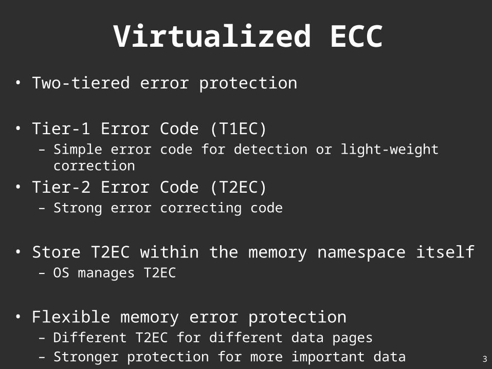
Virtualized ECC• Two-tiered error protection
• Tier-1 Error Code (T1EC)– Simple error code for detection or light-weight correction
• Tier-2 Error Code (T2EC)– Strong error correcting code
• Store T2EC within the memory namespace itself– OS manages T2EC
• Flexible memory error protection– Different T2EC for different data pages– Stronger protection for more important data

4
Virtualized ECC – ExamplePhysical Memory
Data T1EC
Virtual Address space
Low
High
Virtual Page to Physical Frame mapping
Physical Frame to ECC Page mapping
T2EC for Chipkill
T2EC for Double
Chipkill
Page frame – i
Page frame – j
Page frame – k
ECC page – j
ECC page – k
Virtual page – i
Virtual page – j
Virtual page – k
Error Protection
Level

5
VIRTUALIZED ECC
6
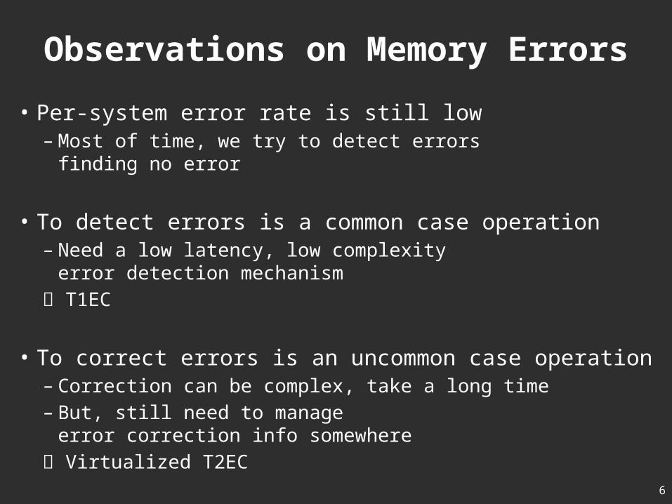
Observations on Memory Errors
• Per-system error rate is still low– Most of time, we try to detect errors
finding no error
• To detect errors is a common case operation– Need a low latency, low complexity
error detection mechanism T1EC
• To correct errors is an uncommon case operation– Correction can be complex, take a long time– But, still need to manage
error correction info somewhere Virtualized T2EC
7
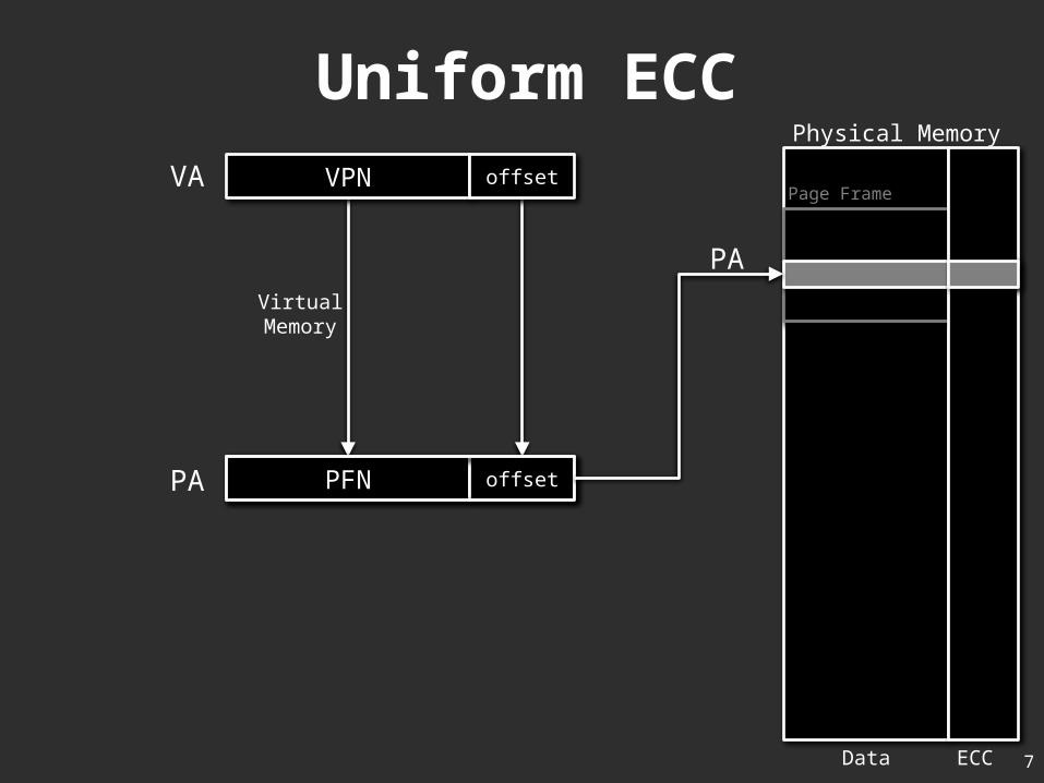
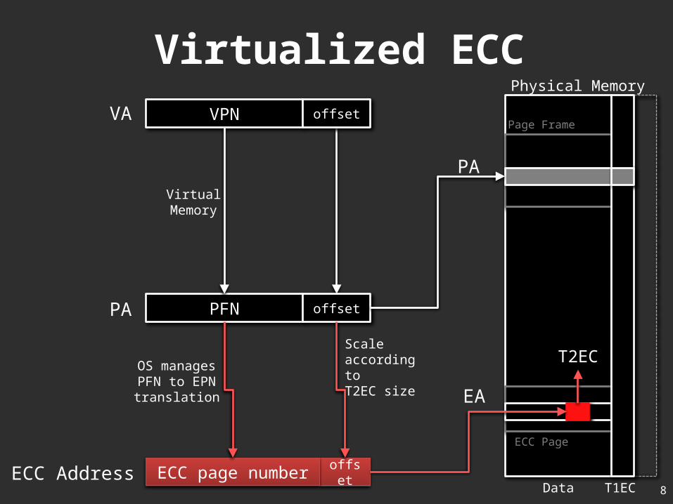
Uniform ECCPhysical Memory
Data ECC
VPN
Virtual Memory
VA offset
PFN offsetPA
Page Frame
PA
8
Virtualized ECCPhysical Memory
Data T1EC
VPNVA offset
PFN offsetPA
Scale according to T2EC size
offsetECC Address
OS managesPFN to EPNtranslation
ECC page number
T2EC
ECC Page
PA
EA
Virtual Memory
Page Frame
Data T1EC Data T1EC
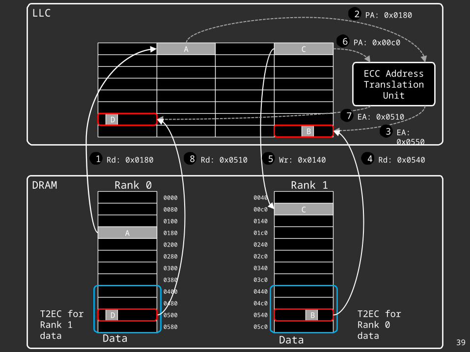
LLC
DRAM Rank 0 Rank 1
ECC Address Translation Unit
T2EC for Rank 1 data
T2EC for Rank 0 data
0000
0080
0100
0180
0200
0280
0300
0380
0400
0480
0500
0580
0040
00c0
0140
01c0
0240
02c0
0340
03c0
0440
04c0
0540
05c0
PA: 0x02003
Wr: 0x02002
B0
B0
Rd: 0x00c01
A
A
B1
B2
B3
1 2 3
1 2 3
EA: 0x054040
0
Wr: 0x05405
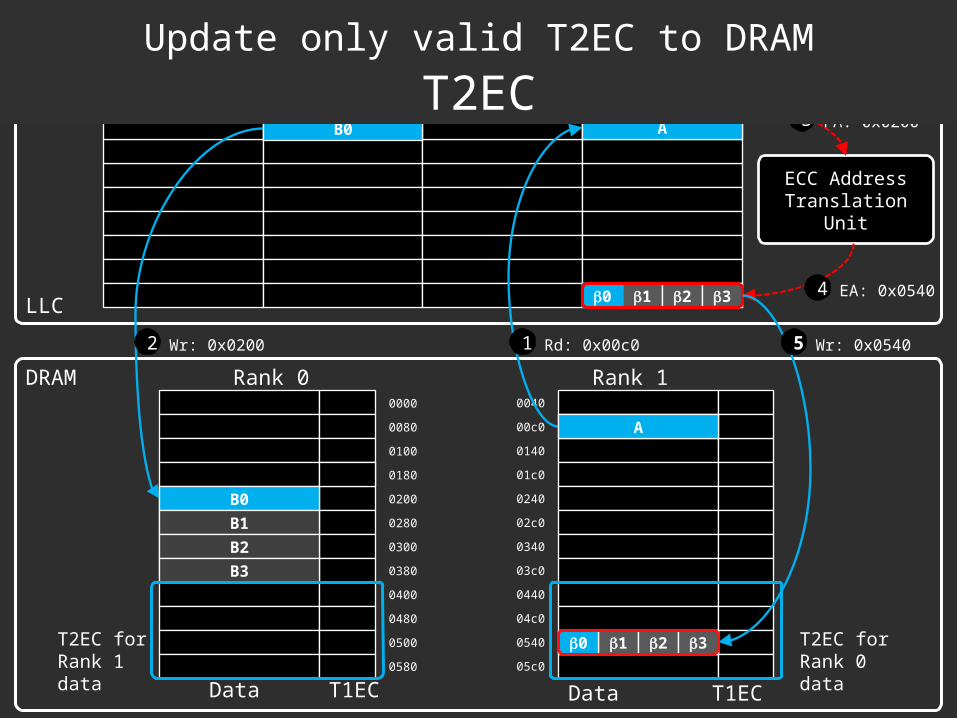
Virtualized ECC operationRead: fetch data and T1ECDon’t need T2EC in most casesWrite: update data, T1EC, and T2ECECC Address Translation Unit: fast PA to EA translationT2ECs of consecutive data lines map to a T2EC lineT2EC lines can be partially validUpdate only valid T2EC to DRAM
10
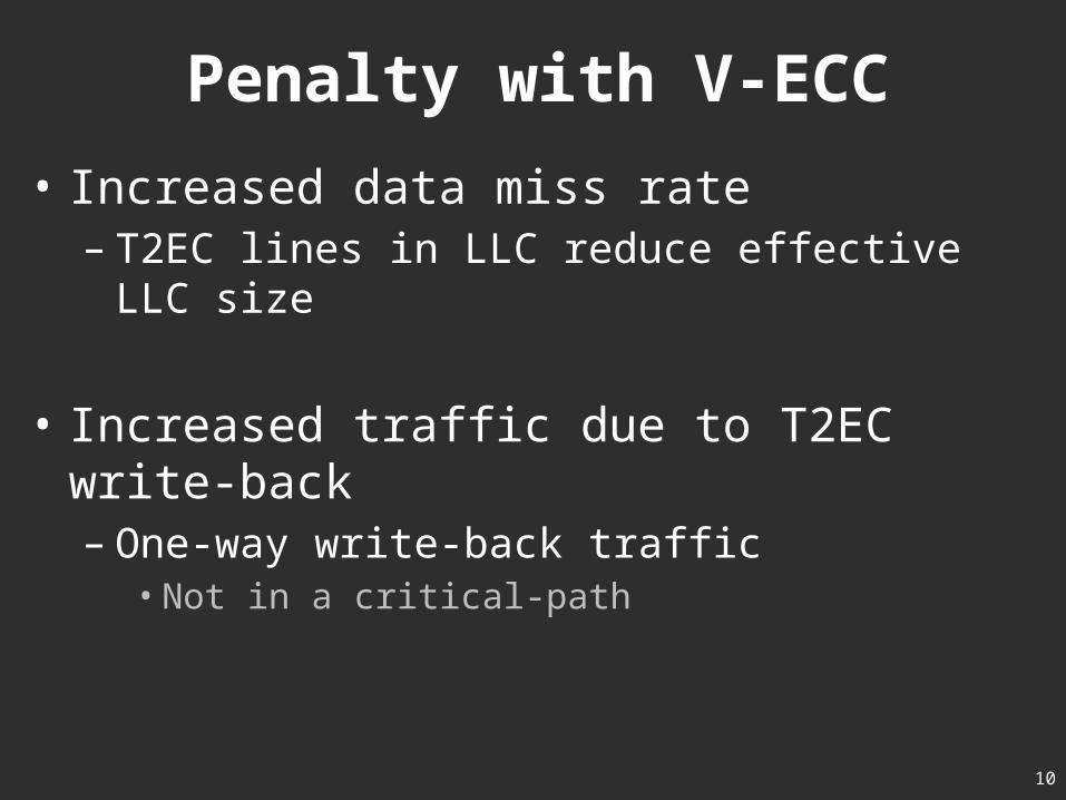
Penalty with V-ECC
• Increased data miss rate– T2EC lines in LLC reduce effective LLC size
• Increased traffic due to T2EC write-back– One-way write-back traffic
• Not in a critical-path

11
CHIPKILL-CORRECT
12
Chipkill-correct
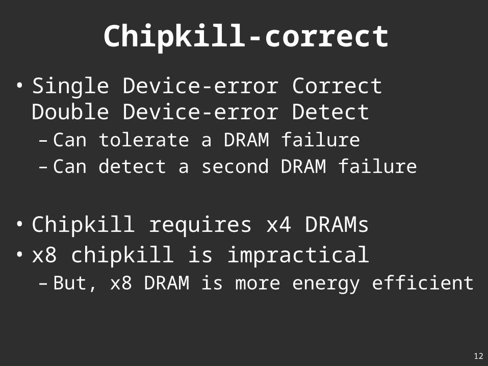
• Single Device-error CorrectDouble Device-error Detect– Can tolerate a DRAM failure– Can detect a second DRAM failure
• Chipkill requires x4 DRAMs• x8 chipkill is impractical
– But, x8 DRAM is more energy efficient
13
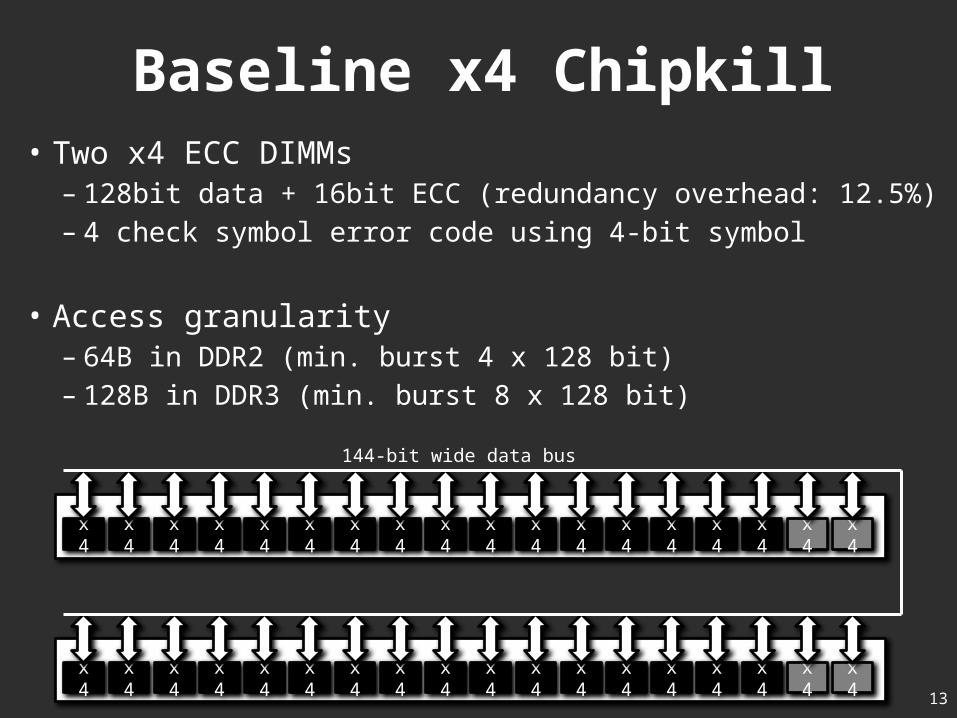
Baseline x4 Chipkill• Two x4 ECC DIMMs
– 128bit data + 16bit ECC (redundancy overhead: 12.5%)– 4 check symbol error code using 4-bit symbol
• Access granularity – 64B in DDR2 (min. burst 4 x 128 bit)– 128B in DDR3 (min. burst 8 x 128 bit)
x4
x4
x4
x4
x4
x4
x4
x4
x4
x4
x4
x4
x4
x4
x4
x4
x4
x4
x4
x4
x4
x4
x4
x4
x4
x4
x4
x4
x4
x4
x4
x4
x4
x4
x4
x4
144-bit wide data bus

14
x8 Chipkill• x8 chipkill with the same access granularity
– 152-bit wide data path• 128-bit data + 24-bit ECC• Redundancy overhead: 18.75%
– Need a custom-designed DIMM• Increase the system cost a lot
152-bit wide data bus
x8 x8 x8 x8 x8 x8 x8 x8 x8
x8 x8 x8 x8 x8 x8 x8 x8 x8
x8

15
x8 Chipkill /w Standard DIMMs• Increase access granularity
– 128B in DDR2 (min. burst 4 x 256 bit)– 256B in DDR3 (min. burst 8 x 256 bit)
x8 x8 x8 x8 x8 x8 x8 x8 x8
x8 x8 x8 x8 x8 x8 x8 x8
x8 x8 x8 x8 x8 x8 x8 x8 x8
x8 x8 x8 x8 x8 x8 x8 x8 x8
280-bit wide data bus

16
V-ECC for Chipkill
• Use 3 check symbol error codes– Single Symbol-error Correct and
Double Symbol-error Detect
• T1EC– 2 check symbols– Detect up to 2 symbol error
• T2EC– 3rd check symbol– Combined T1EC/T2EC provides Chipkill
17
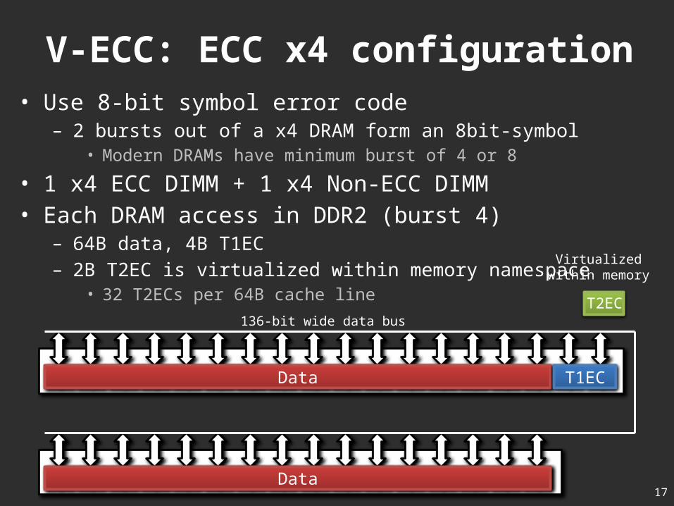
V-ECC: ECC x4 configuration• Use 8-bit symbol error code
– 2 bursts out of a x4 DRAM form an 8bit-symbol• Modern DRAMs have minimum burst of 4 or 8
• 1 x4 ECC DIMM + 1 x4 Non-ECC DIMM• Each DRAM access in DDR2 (burst 4)
– 64B data, 4B T1EC– 2B T2EC is virtualized within memory namespace
• 32 T2ECs per 64B cache line
Virtualized within memory
x4
x4
x4
x4
x4
x4
x4
x4
x4
x4
x4
x4
x4
x4
x4
x4
x4
x4
x4
x4
x4
x4
x4
x4
x4
x4
x4
x4
x4
x4
x4
x4
x4
x4
136-bit wide data bus
Data
Data
T1EC
T2EC
18
144-bit wide data bus
x8 x8 x8 x8 x8 x8 x8 x8 x8
x8 x8 x8 x8 x8 x8 x8 x8 x8
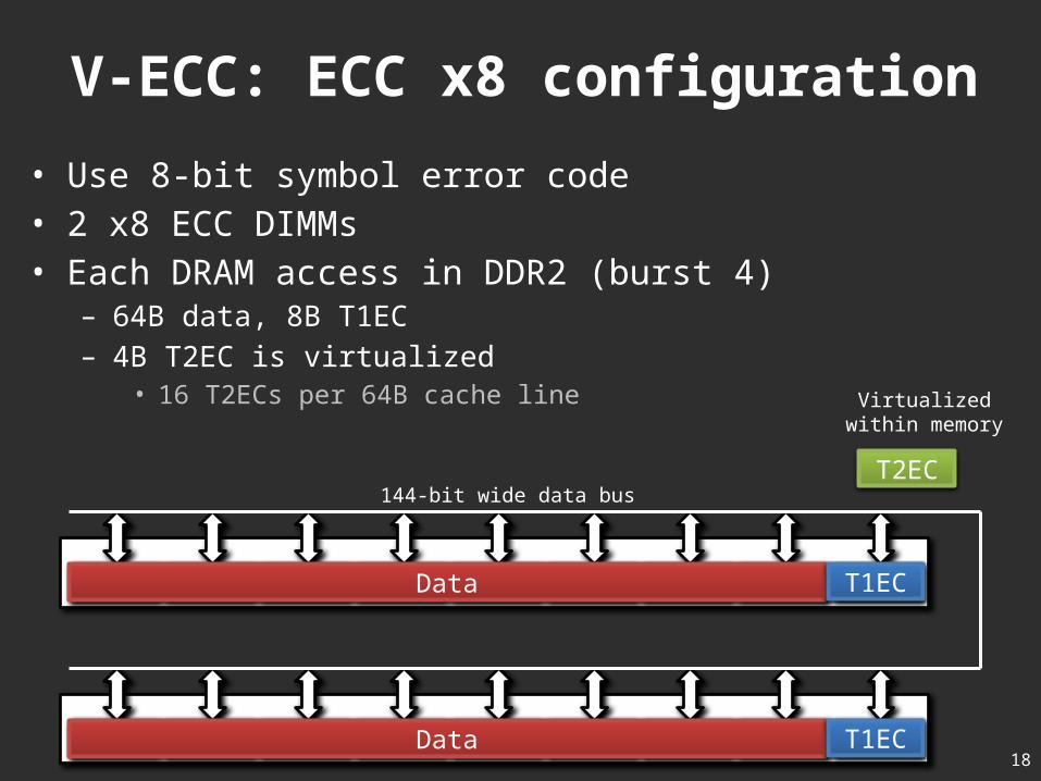
V-ECC: ECC x8 configuration
• Use 8-bit symbol error code• 2 x8 ECC DIMMs• Each DRAM access in DDR2 (burst 4)
– 64B data, 8B T1EC– 4B T2EC is virtualized
• 16 T2ECs per 64B cache line
Data
Data
T1EC
T1EC
T2EC
Virtualized within memory

19
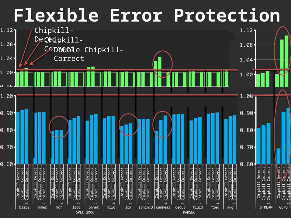
Flexible Error Protection• Single HW with V-ECC can provide
– Chipkill-detect, Chipkill-correct, and Double chipkill-correct
– Use different T2EC for different pages
• Reliability – Performance tradeoff
• Maximize performance/power efficiency with Chipkill-Detect
• Stronger protection at the cost of additional T2EC access
Chipkill-Detect
Chipkill-Correct
Double Chipkill-Correct
ECC x4 0B 2B 4B
ECC x8 0B 4B 8B

20
EVALUATION
21
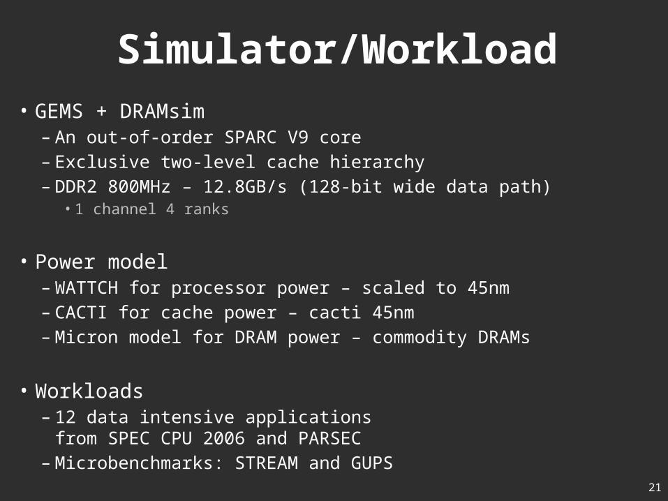
Simulator/Workload• GEMS + DRAMsim
– An out-of-order SPARC V9 core– Exclusive two-level cache hierarchy– DDR2 800MHz – 12.8GB/s (128-bit wide data path)
• 1 channel 4 ranks
• Power model– WATTCH for processor power – scaled to 45nm– CACTI for cache power – cacti 45nm– Micron model for DRAM power – commodity DRAMs
• Workloads– 12 data intensive applications
from SPEC CPU 2006 and PARSEC– Microbenchmarks: STREAM and GUPS
bzi
p2
hm
me
r
mcf
libq
om
ne
t
milc
lbm
sph
inx3
can
ne
al
de
du
p
fluid
fre
q
avg
SPEC 2006 PARSEC
0.94
0.96
0.98
1.00
1.02
1.04
1.06
1.08
1.10
Baseline x4 ECC x4 ECC x8
STREAM GUPS
0.94
0.96
0.98
1.00
1.02
1.04
1.06
1.08
1.10
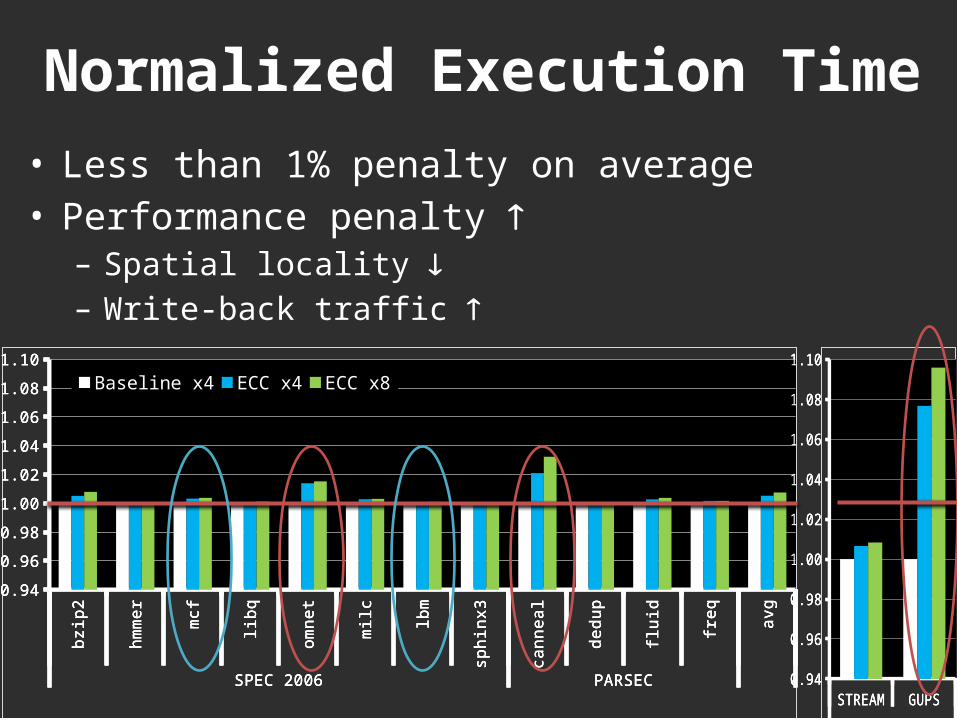
Normalized Execution Time• Less than 1% penalty on average• Performance penalty
– Spatial locality – Write-back traffic
bzi
p2
hm
me
r
mcf
libq
om
ne
t
milc
lbm
sph
inx3
can
ne
al
de
du
p
fluid
fre
q
avg
SPEC 2006 PARSEC
0.94
0.96
0.98
1.00
1.02
1.04
1.06
1.08
1.10
Baseline x4 ECC x4 ECC x8
STREAM GUPS
0.94
0.96
0.98
1.00
1.02
1.04
1.06
1.08
1.10
bzi
p2
hm
me
r
mcf
libq
om
ne
t
milc
lbm
sph
inx3
can
ne
al
de
du
p
fluid
fre
q
avg
SPEC 2006 PARSEC
0.94
0.96
0.98
1.00
1.02
1.04
1.06
1.08
1.10
Baseline x4 ECC x4 ECC x8
STREAM GUPS
0.94
0.96
0.98
1.00
1.02
1.04
1.06
1.08
1.10

bzi
p2
hm
me
r
mcf
libq
om
ne
t
milc
lbm
sph
inx3
can
ne
al
de
du
p
fluid
fre
q
avg
SPEC 2006 PARSEC
0.60
0.65
0.70
0.75
0.80
0.85
0.90
0.95
1.00
1.05
1.10
Baseline x4 ECC x4 ECC x8
ST
RE
AM
GU
PS
0.60
0.65
0.70
0.75
0.80
0.85
0.90
0.95
1.00
1.05
1.10
System Energy Efficiency
• Energy Delay Product (EDP) gain– ECC x4: 1.1% on average– ECC x8: 12.0% on average
bzi
p2
hm
me
r
mcf
libq
om
ne
t
milc
lbm
sph
inx3
can
ne
al
de
du
p
fluid
fre
q
avg
SPEC 2006 PARSEC
0.60
0.65
0.70
0.75
0.80
0.85
0.90
0.95
1.00
1.05
1.10
Baseline x4 ECC x4 ECC x8
ST
RE
AM
GU
PS
0.60
0.65
0.70
0.75
0.80
0.85
0.90
0.95
1.00
1.05
1.101.23
ST
RE
AM
GU
PS
0.60
0.65
0.70
0.75
0.80
0.85
0.90
0.95
1.00
1.05
1.10
bzi
p2
hm
me
r
mcf
libq
om
ne
t
milc
lbm
sph
inx3
can
ne
al
de
du
p
fluid
fre
q
avg
SPEC 2006 PARSEC
0.60
0.65
0.70
0.75
0.80
0.85
0.90
0.95
1.00
1.05
1.10
Baseline x4 ECC x4 ECC x8
20%17%
10%12%
0.96
1.00
1.04
1.08
1.12
Flexible Error Protection
1234560.96
1.00
1.04
1.08
1.12
Ch
ipki
ll D
ete
ctC
hip
kill
Co
rre
ct2
Ch
ipki
ll C
orr
ect
Ch
ipki
ll D
ete
ctC
hip
kill
Co
rre
ct2
Ch
ipki
ll C
orr
ect
Ch
ipki
ll D
ete
ctC
hip
kill
Co
rre
ct2
Ch
ipki
ll C
orr
ect
Ch
ipki
ll D
ete
ctC
hip
kill
Co
rre
ct2
Ch
ipki
ll C
orr
ect
Ch
ipki
ll D
ete
ctC
hip
kill
Co
rre
ct2
Ch
ipki
ll C
orr
ect
Ch
ipki
ll D
ete
ctC
hip
kill
Co
rre
ct2
Ch
ipki
ll C
orr
ect
Ch
ipki
ll D
ete
ctC
hip
kill
Co
rre
ct2
Ch
ipki
ll C
orr
ect
Ch
ipki
ll D
ete
ctC
hip
kill
Co
rre
ct2
Ch
ipki
ll C
orr
ect
Ch
ipki
ll D
ete
ctC
hip
kill
Co
rre
ct2
Ch
ipki
ll C
orr
ect
Ch
ipki
ll D
ete
ctC
hip
kill
Co
rre
ct2
Ch
ipki
ll C
orr
ect
Ch
ipki
ll D
ete
ctC
hip
kill
Co
rre
ct2
Ch
ipki
ll C
orr
ect
Ch
ipki
ll D
ete
ctC
hip
kill
Co
rre
ct2
Ch
ipki
ll C
orr
ect
Ch
ipki
ll D
ete
ctC
hip
kill
Co
rre
ct2
Ch
ipki
ll C
orr
ect
bzip2 hmmer mcf libq omnet milc lbm sphinx3 canneal dedup fluid freq avgSPEC 2006 PARSEC
0.60
0.70
0.80
0.90
1.00Normalized EDP
Ch
ipki
ll D
ete
ctC
hip
kill
Co
rre
ct2
Ch
ipki
ll C
orr
ect
Ch
ipki
ll D
ete
ctC
hip
kill
Co
rre
ct2
Ch
ipki
ll C
orr
ect
STREAM GUPS
0.60
0.70
0.80
0.90
1.00
Chipkill-DetectChipkill-Correct
Double Chipkill-Correct

25
Conclusion• Virtualized ECC
– Two-tiered error protection, virtualized T2EC
• Improved system energy efficiency with chipkill– Reduce DRAM power consumption by 27%– Improve system EDP by 12%
• Performance penalty – 1% on average
• Error protection even for Non-ECC DIMMs– Can be used for GPU memory error protection
• Flexibility in error protection– Adaptive error protection level by user/system demand– Cost of error protection is proportional to protection level

26
Virtualized and Flexible ECC for Main Memory
Doe Hyun Yoon and Mattan Erez
Dept. Electrical and Computer Engineering The University of Texas at Austin

27
BACKUP
28
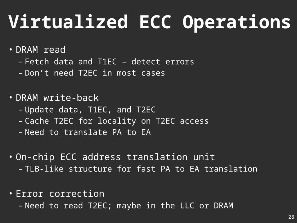
Virtualized ECC Operations• DRAM read
– Fetch data and T1EC – detect errors– Don’t need T2EC in most cases
• DRAM write-back– Update data, T1EC, and T2EC– Cache T2EC for locality on T2EC access– Need to translate PA to EA
• On-chip ECC address translation unit– TLB-like structure for fast PA to EA translation
• Error correction– Need to read T2EC; maybe in the LLC or DRAM

29Data T1EC Data T1EC
LLC
DRAM Rank 0 Rank 1
ECC Address Translation Unit
T2EC for Rank 1 data
T2EC for Rank 0 data
0000
0080
0100
0180
0200
0280
0300
0380
0400
0480
0500
0580
0040
00c0
0140
01c0
0240
02c0
0340
03c0
0440
04c0
0540
05c0
PA: 0x02003
Wr: 0x02002
B0
B0
Rd: 0x00c01
A
A
B1
B2
B3
1 2 3
1 2 3
EA: 0x054040
0
Wr: 0x05405
30
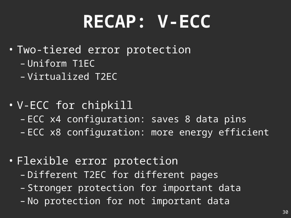
RECAP: V-ECC
• Two-tiered error protection– Uniform T1EC– Virtualized T2EC
• V-ECC for chipkill– ECC x4 configuration: saves 8 data pins– ECC x8 configuration: more energy efficient
• Flexible error protection– Different T2EC for different pages– Stronger protection for important data– No protection for not important data

Ba
selin
e x
4E
CC
x4
EC
C x
8
Ba
selin
e x
4E
CC
x4
EC
C x
8
Ba
selin
e x
4E
CC
x4
EC
C x
8
Ba
selin
e x
4E
CC
x4
EC
C x
8
Ba
selin
e x
4E
CC
x4
EC
C x
8
Ba
selin
e x
4E
CC
x4
EC
C x
8
Ba
selin
e x
4E
CC
x4
EC
C x
8
Ba
selin
e x
4E
CC
x4
EC
C x
8
Ba
selin
e x
4E
CC
x4
EC
C x
8
Ba
selin
e x
4E
CC
x4
EC
C x
8
Ba
selin
e x
4E
CC
x4
EC
C x
8
Ba
selin
e x
4E
CC
x4
EC
C x
8
Ba
selin
e x
4E
CC
x4
EC
C x
8
Ba
selin
e x
4E
CC
x4
EC
C x
8
Ba
selin
e x
4E
CC
x4
EC
C x
8
bzip2 hmmer mcf libq omnet milc lbm sphinx3
canneal
dedup fluid freq avg STREAM
GUPS
SPEC 2006 PARSEC
0
5
10
15
20
25
30
DRAM LLC Core Normalized EDP
Sys
tem
Po
we
r [W
]
Ba
selin
e x
4E
CC
x4
EC
C x
8
Ba
selin
e x
4E
CC
x4
EC
C x
8
STREAM GUPS
0
5
10
15
20
25
Sys
tem
Po
we
r [W
]
Power Consumption• DRAM power saving
– ECC x4: 4.2%– ECC x8: 27.8%
• Total power saving– ECC x4: 2.1%– ECC x8: 13.2%
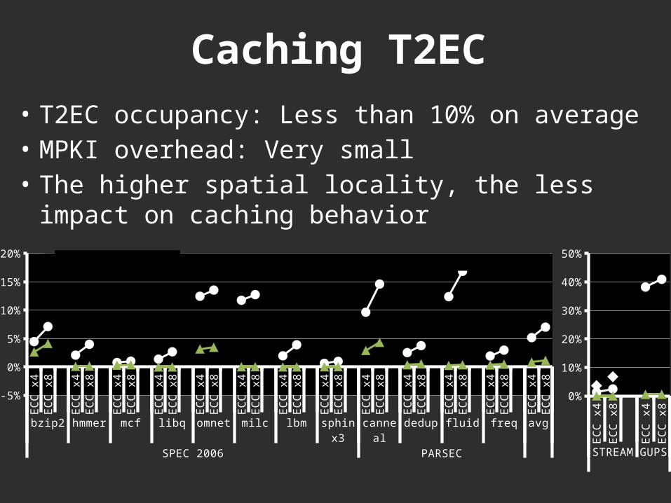
Caching T2EC• T2EC occupancy: Less than 10% on average• MPKI overhead: Very small• The higher spatial locality, the less impact on
caching behavior
EC
C x
4E
CC
x8
EC
C x
4E
CC
x8
EC
C x
4E
CC
x8
EC
C x
4E
CC
x8
EC
C x
4E
CC
x8
EC
C x
4E
CC
x8
EC
C x
4E
CC
x8
EC
C x
4E
CC
x8
EC
C x
4E
CC
x8
EC
C x
4E
CC
x8
EC
C x
4E
CC
x8
EC
C x
4E
CC
x8
EC
C x
4E
CC
x8
bzip2 hmmer mcf libq omnet milc lbm sphinx3 canneal dedup fluid freq avgSPEC 2006 PARSEC
-5%
0%
5%
10%
15%
20%T2EC Miss Rate T2EC occupancy Normalized MPKI Overhead
EC
C x
4
EC
C x
8
EC
C x
4
EC
C x
8
STREAM
GUPS
0%
10%
20%
30%
40%
50%

Bas
elin
e x4
EC
C x
4E
CC
x8
Bas
elin
e x4
EC
C x
4E
CC
x8
Bas
elin
e x4
EC
C x
4E
CC
x8
Bas
elin
e x4
EC
C x
4E
CC
x8
Bas
elin
e x4
EC
C x
4E
CC
x8
Bas
elin
e x4
EC
C x
4E
CC
x8
Bas
elin
e x4
EC
C x
4E
CC
x8
Bas
elin
e x4
EC
C x
4E
CC
x8
Bas
elin
e x4
EC
C x
4E
CC
x8
Bas
elin
e x4
EC
C x
4E
CC
x8
Bas
elin
e x4
EC
C x
4E
CC
x8
Bas
elin
e x4
EC
C x
4E
CC
x8
Bas
elin
e x4
EC
C x
4E
CC
x8
bzip2 hmmer mcf libq omnet milc lbm sphinx3 canneal dedup fluid freq avgSPEC 2006 PARSEC
0
5
10
15
20
25
0%
5%
10%
15%
20%
25%
T2EC Wr Rd Traffic Increase
Re
qu
est
pe
r K
I
Tra
ffic
Incr
ea
se
Bas
elin
e x4
EC
C x
4E
CC
x8
Bas
elin
e x4
EC
C x
4E
CC
x8
STREAM
GUPS
0
50
100
150
200
250
300
0%
10%
20%
30%
40%
50%
60%
Re
qu
est
pe
r K
I
Tra
ffic
Incr
ea
se
Traffic• Traffic increase – less than 10% on average
– Increased demand misses; – T2EC traffic
• Spatial locality is important, so is the amount of write-back traffic
34
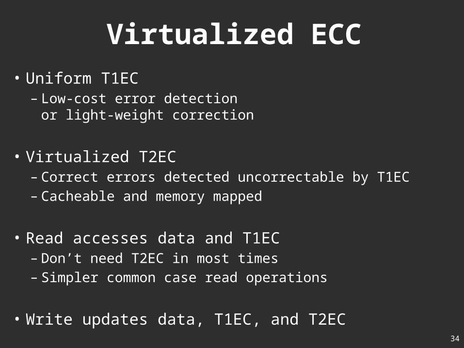
Virtualized ECC• Uniform T1EC
– Low-cost error detection or light-weight correction
• Virtualized T2EC– Correct errors detected uncorrectable by T1EC– Cacheable and memory mapped
• Read accesses data and T1EC– Don’t need T2EC in most times– Simpler common case read operations
• Write updates data, T1EC, and T2EC
35
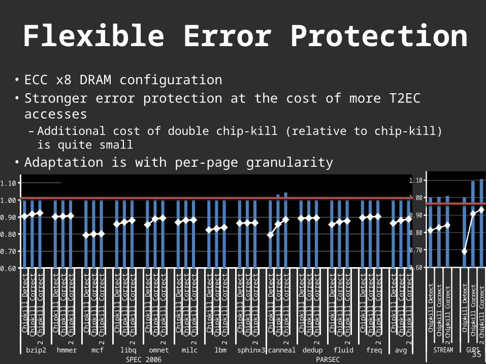
Flexible Error Protection• ECC x8 DRAM configuration• Stronger error protection at the cost of more T2EC accesses
– Additional cost of double chip-kill (relative to chip-kill)is quite small
• Adaptation is with per-page granularity
Ch
ipki
ll D
ete
ctC
hip
kill
Co
rre
ct2
Ch
ipki
ll C
orr
ect
Ch
ipki
ll D
ete
ctC
hip
kill
Co
rre
ct2
Ch
ipki
ll C
orr
ect
Ch
ipki
ll D
ete
ctC
hip
kill
Co
rre
ct2
Ch
ipki
ll C
orr
ect
Ch
ipki
ll D
ete
ctC
hip
kill
Co
rre
ct2
Ch
ipki
ll C
orr
ect
Ch
ipki
ll D
ete
ctC
hip
kill
Co
rre
ct2
Ch
ipki
ll C
orr
ect
Ch
ipki
ll D
ete
ctC
hip
kill
Co
rre
ct2
Ch
ipki
ll C
orr
ect
Ch
ipki
ll D
ete
ctC
hip
kill
Co
rre
ct2
Ch
ipki
ll C
orr
ect
Ch
ipki
ll D
ete
ctC
hip
kill
Co
rre
ct2
Ch
ipki
ll C
orr
ect
Ch
ipki
ll D
ete
ctC
hip
kill
Co
rre
ct2
Ch
ipki
ll C
orr
ect
Ch
ipki
ll D
ete
ctC
hip
kill
Co
rre
ct2
Ch
ipki
ll C
orr
ect
Ch
ipki
ll D
ete
ctC
hip
kill
Co
rre
ct2
Ch
ipki
ll C
orr
ect
Ch
ipki
ll D
ete
ctC
hip
kill
Co
rre
ct2
Ch
ipki
ll C
orr
ect
Ch
ipki
ll D
ete
ctC
hip
kill
Co
rre
ct2
Ch
ipki
ll C
orr
ect
bzip2 hmmer mcf libq omnet milc lbm sphinx3 canneal dedup fluid freq avgSPEC 2006 PARSEC
0.60
0.70
0.80
0.90
1.00
1.10 Normalized Execution Time Normalized EDP
Chi
pkill
Det
ect
Chi
pkill
Cor
rect
2 C
hipk
ill C
orre
ct
Chi
pkill
Det
ect
Chi
pkill
Cor
rect
2 C
hipk
ill C
orre
ct
STREAM GUPS
0.60
0.70
0.80
0.90
1.00
1.10

36
What if BW is limited?
• Half DRAM BW – 6.4GB/s• Emulate CMP where BW is more scarce
Bas
elin
e x4
EC
C x
8
Bas
elin
e x4
EC
C x
8
Bas
elin
e x4
EC
C x
8
Bas
elin
e x4
EC
C x
8
Bas
elin
e x4
EC
C x
8
Bas
elin
e x4
EC
C x
8
Bas
elin
e x4
EC
C x
8
Bas
elin
e x4
EC
C x
8
Bas
elin
e x4
EC
C x
8
Bas
elin
e x4
EC
C x
8
Bas
elin
e x4
EC
C x
8
Bas
elin
e x4
EC
C x
8
Bas
elin
e x4
EC
C x
8
bzip2 hmmer mcf libq omnet milc lbm sphinx3 canneal dedup fluid freq AvgSPEC 2006 PARSEC
0.700000000000001
0.750000000000001
0.800000000000001
0.850000000000001
0.900000000000001
0.950000000000001
1
1.05
1.1Normalized Execution Time Normalized EDP
Bas
elin
e x4
EC
C x
8
Bas
elin
e x4
EC
C x
8
STREAM GUPS
0
0.2
0.4
0.6
0.8
1
1.2
1.4

37
VIRTUALIZED ECC FOR NON-ECC DIMMS

38
ECC for non-ECC DIMMs
• Virtualize ECC in memory namespace– Not a two-tiered error protection– No uniform ECC storage (for T1EC)– But, let’s say the ECC as ‘T2EC’ to keep notation
consistent
• Virtualized T2EC both detects and corrects errors– Now, a DRAM read also triggers a T2EC access– Increased T2EC traffic, increased T2EC
occupancy, and more penalty– But, we can detect and correct errors with non-
ECC DIMMs
39
A
A
Data Data
LLC
DRAM Rank 0 Rank 1
ECC Address Translation Unit
B
BT2EC for Rank 1 data
0000
0080
0100
0180
0200
0280
0300
0380
0400
0480
0500
0580
0040
00c0
0140
01c0
0240
02c0
0340
03c0
0440
04c0
0540
05c0
Rd: 0x01801
PA: 0x01802
EA: 0x05503
Rd: 0x05404
C
C
T2EC for Rank 0 data
Wr: 0x01405
D
PA: 0x00c06
EA: 0x05107
D
Rd: 0x05108
40
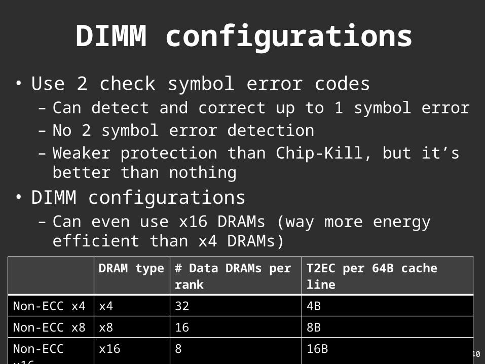
DIMM configurations• Use 2 check symbol error codes
– Can detect and correct up to 1 symbol error– No 2 symbol error detection– Weaker protection than Chip-Kill, but it’s better
than nothing
• DIMM configurations– Can even use x16 DRAMs (way more energy
efficient than x4 DRAMs)DRAM type # Data DRAMs per rank T2EC per 64B cache line
Non-ECC x4 x4 32 4B
Non-ECC x8 x8 16 8B
Non-ECC x16 x16 8 16B

41
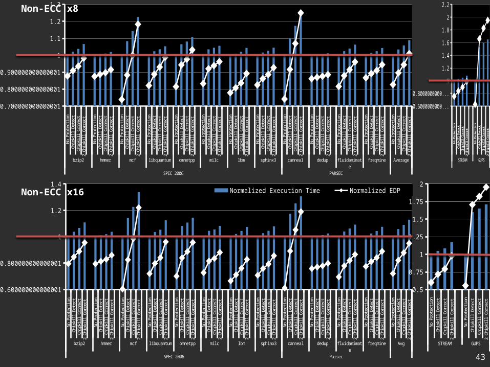
Performance and Energy Efficiency
• More performance degradation (compared to ECC DIMMs)– Every read accesses T2EC– More T2EC traffic more T2EC occupancy in LLC
• Energy efficiency is sometimes better– x16 DRAMs save a lot of DRAM power– Performance degradation is low if spatial locality is good
Bas
elin
e x4
Non
-EC
C x
4N
on-E
CC
x8
Non
-EC
C x
16
Bas
elin
e x4
Non
-EC
C x
4N
on-E
CC
x8
Non
-EC
C x
16
Bas
elin
e x4
Non
-EC
C x
4N
on-E
CC
x8
Non
-EC
C x
16
Bas
elin
e x4
non-
EC
C x
4no
n-E
CC
x8
non-
EC
C x
16
Bas
elin
e x4
Non
-EC
C x
4N
on-E
CC
x8
Non
-EC
C x
16
Bas
elin
e x4
Non
-EC
C x
4N
on-E
CC
x8
Non
-EC
C x
16
Bas
elin
e x4
Non
-EC
C x
4N
on-E
CC
x8
Non
-EC
C x
16
Bas
elin
e x4
Non
-EC
C x
4N
on-E
CC
x8
Non
-EC
C x
16
Bas
elin
e x4
Non
-EC
C x
4N
on-E
CC
x8
Non
-EC
C x
16
Bas
elin
e x4
Non
-EC
C x
4N
on-E
CC
x8
Non
-EC
C x
16
Bas
elin
e x4
Non
-EC
C x
4N
on-E
CC
x8
Non
-EC
C x
16
Bas
elin
e x4
Non
-EC
C x
4N
on-E
CC
x8
Non
-EC
C x
16
Bas
elin
e x4
Non
-EC
C x
4N
on-E
CC
x8
Non
-EC
C x
16
bzip2 hmmer mcf libquantum omnetpp milc lbm sphinx3 canneal dedup fluidanimate freqmine AverageSPEC 2006 PARSEC
0.700000000000001
0.800000000000001
0.900000000000001
1
1.1
1.2
1.3Normalized Execution Time Normalized EDP
Bas
elin
e x4
Non
-EC
C x
4
Non
-EC
C x
8
Non
-EC
C x
16
Bas
elin
e x4
Non
-EC
C x
4
Non
-EC
C x
8
Non
-EC
C x
16
STREAM GUPS
0
0.5
1
1.5
2
2.5
3
42
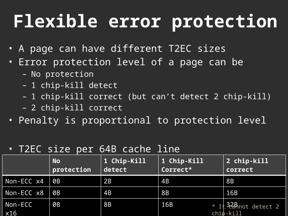
Flexible error protection• A page can have different T2EC sizes• Error protection level of a page can be
– No protection– 1 chip-kill detect– 1 chip-kill correct (but can’t detect 2 chip-kill)– 2 chip-kill correct
• Penalty is proportional to protection level
• T2EC size per 64B cache lineNo protection 1 Chip-Kill detect 1 Chip-Kill Correct* 2 chip-kill correct
Non-ECC x4 0B 2B 4B 8B
Non-ECC x8 0B 4B 8B 16B
Non-ECC x16 0B 8B 16B 32B
* It cannot detect 2 chip-kill
43
No
Pro
tect
ion
Chi
pkill
Det
ect
Chi
pkill
Cor
rect
2 C
hipk
ill C
orre
ct
No
Pro
tect
ion
Chi
pkill
Det
ect
Chi
pkill
Cor
rect
2 C
hipk
ill C
orre
ct
No
Pro
tect
ion
Chi
pkill
Det
ect
Chi
pkill
Cor
rect
2 C
hipk
ill C
orre
ct
No
Pro
tect
ion
Chi
pkill
Det
ect
Chi
pkill
Cor
rect
2 C
hipk
ill C
orre
ct
No
Pro
tect
ion
Chi
pkill
Det
ect
Chi
pkill
Cor
rect
2 C
hipk
ill C
orre
ct
No
Pro
tect
ion
Chi
pkill
Det
ect
Chi
pkill
Cor
rect
2 C
hipk
ill C
orre
ct
No
Pro
tect
ion
Chi
pkill
Det
ect
Chi
pkill
Cor
rect
2 C
hipk
ill C
orre
ct
No
Pro
tect
ion
Chi
pkill
Det
ect
Chi
pkill
Cor
rect
2 C
hipk
ill C
orre
ct
No
Pro
tect
ion
Chi
pkill
Det
ect
Chi
pkill
Cor
rect
2 C
hipk
ill C
orre
ct
No
Pro
tect
ion
Chi
pkill
Det
ect
Chi
pkill
Cor
rect
2 C
hipk
ill C
orre
ct
No
Pro
tect
ion
Chi
pkill
Det
ect
Chi
pkill
Cor
rect
2 C
hipk
ill C
orre
ct
No
Pro
tect
ion
Chi
pkill
Det
ect
Chi
pkill
Cor
rect
2 C
hipk
ill C
orre
ct
No
Pro
tect
ion
Chi
pkill
Det
ect
Chi
pkill
Cor
rect
2 C
hipk
ill C
orre
ct
bzip2 hmmer mcf libquantum omnetpp milc lbm sphinx3 canneal dedup fluidanimate freqmine AvgSPEC 2006 Parsec
0.600000000000001
0.800000000000001
1
1.2
1.4Normalized Execution Time Normalized EDP
No
Pro
tect
ion
Chi
pkill
Det
ect
Chi
pkill
Cor
rect
2 C
hipk
ill C
orre
ct
No
Pro
tect
ion
Chi
pkill
Det
ect
Chi
pkill
Cor
rect
2 C
hipk
ill C
orre
ct
STREAM GUPS
0.5
0.75
1
1.25
1.5
1.75
2
No
Pro
tect
ion
Chi
pkill
Det
ect
Chi
pkill
Cor
rect
2 C
hipk
ill C
orre
ct
No
Pro
tect
ion
Chi
pkill
Det
ect
Chi
pkill
Cor
rect
2 C
hipk
ill C
orre
ct
No
Pro
tect
ion
Chi
pkill
Det
ect
Chi
pkill
Cor
rect
2 C
hipk
ill C
orre
ct
No
Pro
tect
ion
Chi
pkill
Det
ect
Chi
pkill
Cor
rect
2 C
hipk
ill C
orre
ct
No
Pro
tect
ion
Chi
pkill
Det
ect
Chi
pkill
Cor
rect
2 C
hipk
ill C
orre
ct
No
Pro
tect
ion
Chi
pkill
Det
ect
Chi
pkill
Cor
rect
2 C
hipk
ill C
orre
ct
No
Pro
tect
ion
Chi
pkill
Det
ect
Chi
pkill
Cor
rect
2 C
hipk
ill C
orre
ct
No
Pro
tect
ion
Chi
pkill
Det
ect
Chi
pkill
Cor
rect
2 C
hipk
ill C
orre
ct
No
Pro
tect
ion
Chi
pkill
Det
ect
Chi
pkill
Cor
rect
2 C
hipk
ill C
orre
ct
No
Pro
tect
ion
Chi
pkill
Det
ect
Chi
pkill
Cor
rect
2 C
hipk
ill C
orre
ct
No
Pro
tect
ion
Chi
pkill
Det
ect
Chi
pkill
Cor
rect
2 C
hipk
ill C
orre
ct
No
Pro
tect
ion
Chi
pkill
Det
ect
Chi
pkill
Cor
rect
2 C
hipk
ill C
orre
ct
No
Pro
tect
ion
Chi
pkill
Det
ect
Chi
pkill
Cor
rect
2 C
hipk
ill C
orre
ct
bzip2 hmmer mcf libquantum omnetpp milc lbm sphinx3 canneal dedup fluidanimate freqmine AverageSPEC 2006 PARSEC
0.700000000000001
0.800000000000001
0.900000000000001
1
1.1
1.2
1.3
No P
rotec
tion
Chipk
ill De
tect
Chipk
ill Co
rrect
2 Chip
kill C
orrec
t
No P
rotec
tion
Chipk
ill De
tect
Chipk
ill Co
rrect
2 Chip
kill C
orrec
t
STREAM GUPS
0.600000000000001
0.800000000000001
1
1.2
1.4
1.6
1.8
2
2.2Non-ECC x8
Non-ECC x16

44
MANAGING T2EC

45
OS manages T2EC
• PA to EA translation structure• T2EC storage
– Only dirty pages require T2EC (with ECC DIMMs)
• Can use Copy-On-Write T2EC allocation
– Every data page needs T2EC in non-ECC implementation
– Free T2EC when a data page is freed/evicted
46
PA to EA Translation
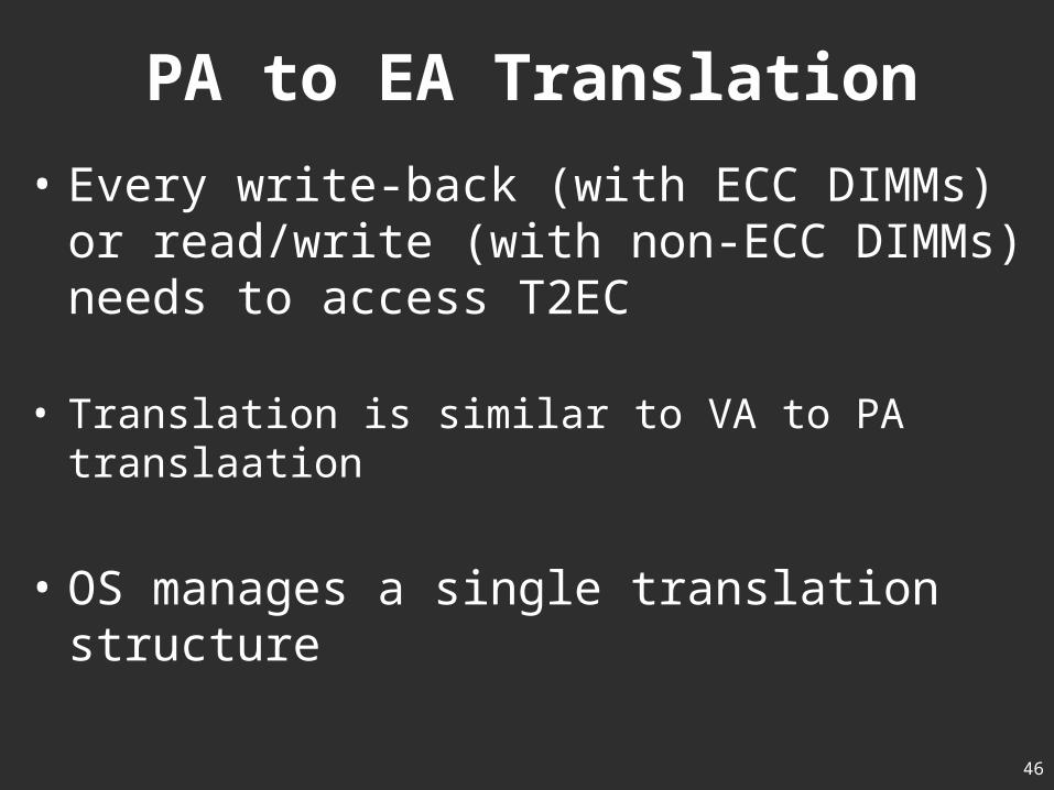
• Every write-back (with ECC DIMMs) or read/write (with non-ECC DIMMs) needs to access T2EC
• Translation is similar to VA to PA translaation
• OS manages a single translation structure
47
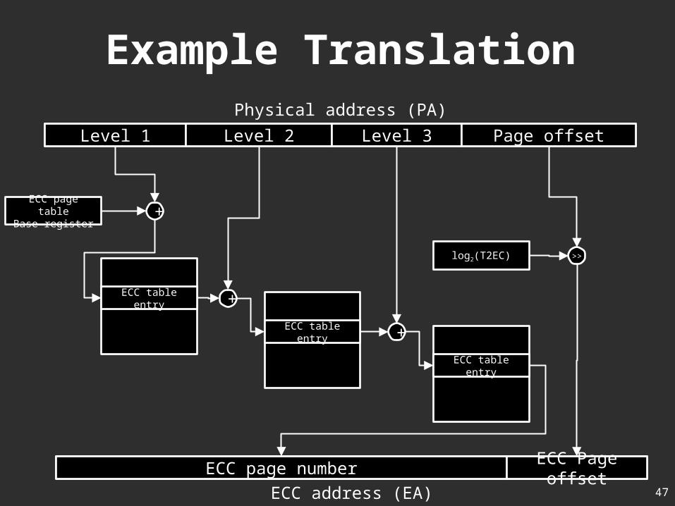
Example Translation
Level 1
Physical address (PA)
Level 2 Level 3 Page offset
ECC page tableBase register +
ECC table entry
ECC table entry
+
ECC table entry
+
ECC page number ECC Page offset
ECC address (EA)
log2(T2EC) >>
48
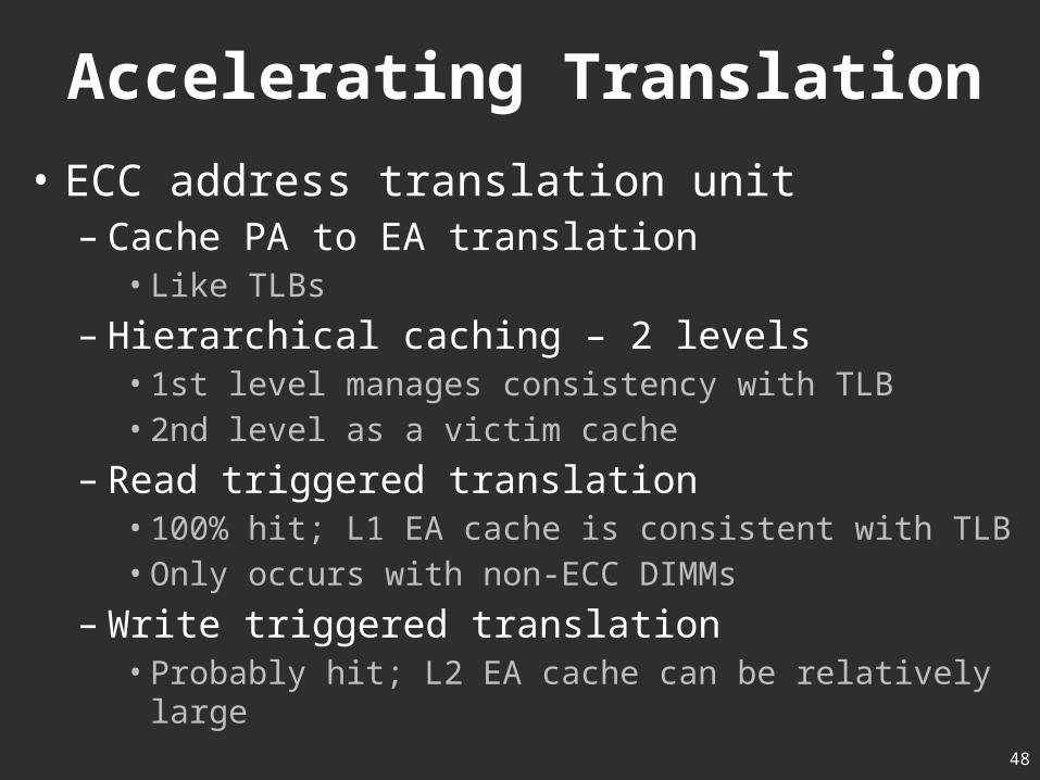
Accelerating Translation
• ECC address translation unit– Cache PA to EA translation
• Like TLBs
– Hierarchical caching – 2 levels• 1st level manages consistency with TLB• 2nd level as a victim cache
– Read triggered translation• 100% hit; L1 EA cache is consistent with TLB• Only occurs with non-ECC DIMMs
– Write triggered translation• Probably hit; L2 EA cache can be relatively large
49
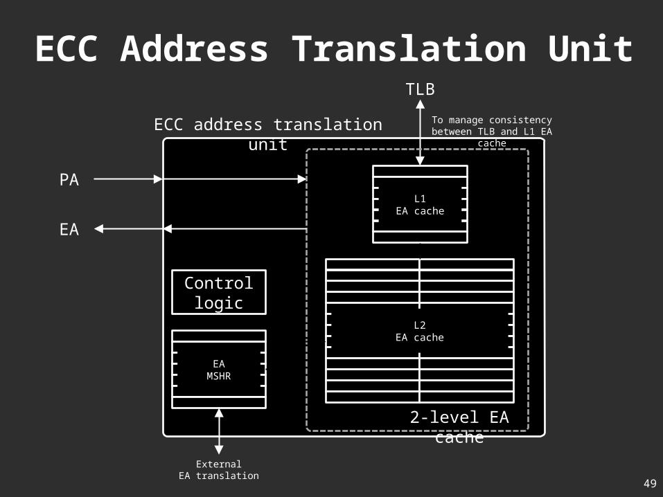
ECC Address Translation Unit
L1EA cache
L2EA cache
2-level EA cache
ECC address translation unit
TLB
To manage consistency between TLB and L1 EA cache
Control logic
PA
EA
EAMSHR
ExternalEA translation

50
Possible Impacts• TLB miss penalty
– VA to PA translation, then PA to EA translation• Seems like negligible – already assumed doubled TLB miss
penalty in the evaluation • Design alternative: to translate VA to EA directly
– Need to manage per-process translation structure– But potentially less impact on TLB miss penalty
• EA cache misses per 1000 instrs– Configuration
• 16 entry FA L1 EA cache• 4k entry 8 way L2 EA cache
– ~3 in omnetpp and canneal– ~12 in GUPS– Less than 1 in other apps– Things might get messed up with a software TLB handler

51
Chip-Kill-Correct• Single device error correct,
Double device error detect– Other names: DRAM RAID, Extended ECC, Advanced
ECC, …– Can tolerate a DRAM device failure
• Using x1 DRAMs
– SEC-DED effectively does chip-kill-correct– But, there’s no x1 DRAM any more (really?)
x1 x1 …x1 x1 x1 x1 x1 x1 x1 x1 x1 x1 x1 x1
64 data bits 8 ECC bits

52
• 4 interleaved SEC-DED – x4 Chip-Kill– 256bit data width– Works with old DRAMs– Modern DRAMs use burst access
• Granularity – DDR2: 128B, DDR3: 256B
Interleaved SEC-DED
x4
64 data DRAMs 8 ECC DRAMs
(72,64) SEC-DED
x4 x4 x4 x4 x4 x4 x4…
(72,64) SEC-DED
(72,64) SEC-DED
(72,64) SEC-DED
…

53
x4 Non ECC-DIMM x4 ECC-DIMM
data
Virtualized
Burst 4
T1EC T2EC
x8 ECC-DIMM x8 ECC-DIMM
data
Virtualized
Burst 4
T1EC T2EC

54
• With the same access granularity– Higher redundancy overhead
• 128-bit data + 24-bit ECC (18.75%)
– Need custom-designed DIMMs
• Using standard ECC DIMMs– Wider data-path
• 256-bit data + 24-bit ECC (9.375%)
– Increase access granularity• 128B in DDR2• 256B in DDR3
Why is x8 chipkill impractical?
55
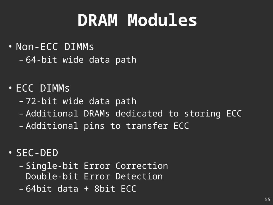
DRAM Modules
• Non-ECC DIMMs– 64-bit wide data path
• ECC DIMMs– 72-bit wide data path– Additional DRAMs dedicated to storing ECC– Additional pins to transfer ECC
• SEC-DED– Single-bit Error Correction
Double-bit Error Detection– 64bit data + 8bit ECC

56
x4
x4
x4
x4
x4
x4
x4
x4
x4
x4
x4
x4
x4
x4
x4
x4
x4 Non-ECC DIMM
x4 ECC DIMM
x4
x4
x4
x4
x4
x4
x4
x4
x4
x4
x4
x4
x4
x4
x4
x4
x4
x4
x8 ECC DIMM
x8 x8 x8 x8 x8 x8 x8 x8 x8
x8 x8 x8 x8 x8 x8 x8 x8
x8 Non-ECC DIMM
64-bit
64-bit
72-bit
72-bit

57
High-end Servers
• Need BOTH reliability and energy efficiency
• Reliability– Chipkill-correct
• But, chipkill requires x4 configurations– Using more energy efficient x8
configurations is impractical with chipkill

58
High-level Memory ModelsVA space
VA
PA space
PA
Data ECC
Program
VA space
VA
PA space
PA
Data T1EC
T2EC
EA
Program
Conventional Architecture Virtualized ECC Architecture
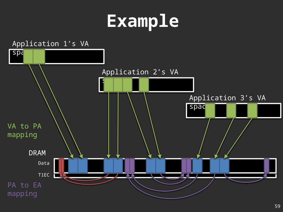
59
ExampleApplication 1’s VA space
Application 2’s VA space
Application 3’s VA space
DRAMData
T1EC
VA to PA mapping
PA to EA mapping
60
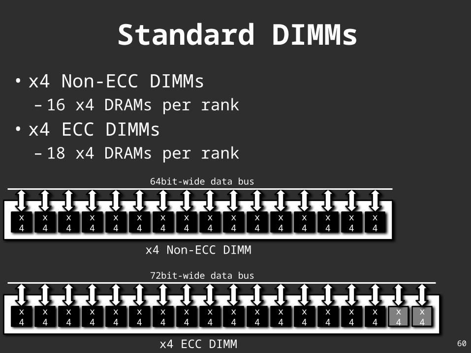
Standard DIMMs
• x4 Non-ECC DIMMs– 16 x4 DRAMs per rank
• x4 ECC DIMMs– 18 x4 DRAMs per rank
x4
x4
x4
x4
x4
x4
x4
x4
x4
x4
x4
x4
x4
x4
x4
x4
64bit-wide data bus
x4 Non-ECC DIMM
72bit-wide data bus
x4 ECC DIMM
x4
x4
x4
x4
x4
x4
x4
x4
x4
x4
x4
x4
x4
x4
x4
x4
x4
x4
61
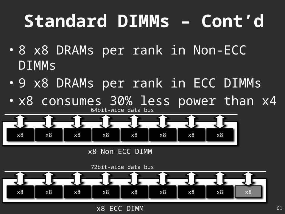
Standard DIMMs – Cont’d
• 8 x8 DRAMs per rank in Non-ECC DIMMs• 9 x8 DRAMs per rank in ECC DIMMs • x8 consumes 30% less power than x4
x8 x8 x8 x8 x8 x8 x8 x8
64bit-wide data bus
x8 Non-ECC DIMM
72bit-wide data bus
x8 ECC DIMM
x8 x8 x8 x8 x8 x8 x8 x8 x8

62
Standard DIMMs – Cont’d
• 4 x16 DRAMs per rank in Non-ECC DIMMs• No x16 ECC DIMMs• More power efficient than x8 DRAMs
NO x16 ECC DIMM
64bit-wide data bus
x16 Non-ECC DIMM
x16 x16 x16 x16
63
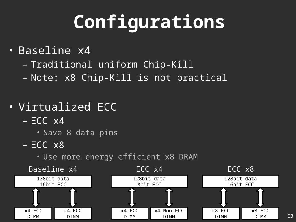
Configurations• Baseline x4
– Traditional uniform Chip-Kill– Note: x8 Chip-Kill is not practical
• Virtualized ECC– ECC x4
• Save 8 data pins
– ECC x8• Use more energy efficient x8 DRAM
128bit data16bit ECC
Baseline x4
x4 ECC DIMM
x4 ECC DIMM
x4 ECC DIMM
x4 Non ECC DIMM
128bit data8bit ECC
x8 ECC DIMM
x8 ECC DIMM
128bit data16bit ECC
ECC x4 ECC x8
64
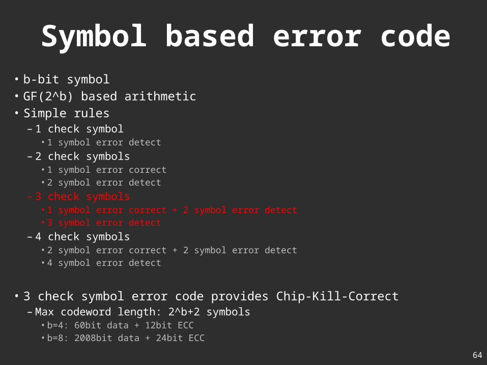
Symbol based error code• b-bit symbol• GF(2^b) based arithmetic• Simple rules
– 1 check symbol• 1 symbol error detect
– 2 check symbols• 1 symbol error correct• 2 symbol error detect
– 3 check symbols• 1 symbol error correct + 2 symbol error detect• 3 symbol error detect
– 4 check symbols• 2 symbol error correct + 2 symbol error detect• 4 symbol error detect
• 3 check symbol error code provides Chip-Kill-Correct– Max codeword length: 2^b+2 symbols
• b=4: 60bit data + 12bit ECC• b=8: 2008bit data + 24bit ECC