vincent t. remcho
TRANSCRIPT

AN ABSTRACT OF THE DISSERTATION OF Carlos F. Gonzalez for the degree of Doctor of Philosophy in Chemistry presented on July 10, 2007. Title: From Electrophoresis to Dielectrophoresis: Designing, Fabricating, and Evaluating an Electroformed Ratchet Type Microfluidic Dielectrophoresis Device Abstract approved:
Vincent T. Remcho
Dielectrophoresis (DEP) is a separation method in which a non-uniform electric
field is used to induce a dipole moment in a suspended particle. If the polarization
of the particle is greater than that of the suspending medium, the particle will move
towards the region of higher field strength (positive DEP); while if the particle is
polarized less than the suspending medium, the particle will be moved towards the
low potential area (negative DEP). In recent years DEP has been gaining
popularity through the construction of microscale devices, and this is due largely
to the decrease in electrode spacing which allows for higher effective field
strengths.
Presented is the design, fabrication, and evaluation of a novel dielectrophoretic
based ratchet device. The electrodes required to produce the asymmetrical field

were constructed of electroformed nickel features grown on the surface of a resist
patterned seedlayer coated glass slide, and this is the first time electroforming has
been used to produce electrodes in the field of DEP. The electrodes were then
made stand alone features located on the glass slide by wet etch removal of the
unplated portions of the seedlayers located on the surface of the glass substrate.
The fluidic component of this device was constructed using replica molding of
poly(dimethylsiloxane), which contained a fluidic reservoir located over the
ratchet electrode features.
Particle selection was conducted using an a priori approach for particles of known
dielectric properties. The frequency responses of perspective test particles to an
asymmetrical electric field were determined through calculation of the real
component of the Clausius-Mossotti factor (Re[K(ω)]). From these calculations,
magnetite and polystyrene spheres were selected as test particles. The device was
then evaluated using the test particles selected to determine if particle collection
occurred in the regions dictated by Re[K(ω)]. Suspensions consisting of single
particle types and a mixture were then evaluated, and it was found that the
particles collected in the regions specified by the theoretical calculations. These
results showed that the device is capable of collecting particles based on the
dielectric properties of the magnetite particles and polystyrene spheres.

© Copyright by Carlos F. Gonzalez July 10, 2007
All Rights Reserved

From Electrophoresis to Dielectrophoresis: Designing, Fabricating, and Evaluating an Electroformed Ratchet Type Microfluidic Dielectrophoresis Device
by Carlos F. Gonzalez
A DISSERATATION
submitted to
Oregon State Universtiy
in partial fulfillment of the requirements for the
degree of
Doctor of Philosophy
Presented July 10, 2007 Commencement June 2008

Doctor of Philosophy dissertation of Carlos F. Gonzalez presented on July 10, 2007.
APPROVED: Major Professor, representing Chemistry Chair of the Department of Chemistry Dean of the Graduate School I understand that my dissertation will become part of the permanent collection of Oregon State University libraries. My signature below authorizes release of my dissertation to any reader upon request.
Carlos F. Gonzalez, Author

ACKNOWLEDGMENTS
I would like to thank Dr. Remcho for the opportunity to work for his research
group. I really appreciate the flexibility he allowed me in my research project no
matter how farfetched my ideas may have been.
I would also like to express my gratitude to my committee members: Dr. Nathan
Ballou, Dr. James Ingle, Dr. Brian Paul, Dr. William Warnes, and Dr. Michael
Schuyler for their guidance through my graduate studies.
Also, I am thankful of Dr. Nathan Ballou for introducing me to the field of
dielectrophoresis.
I would like to acknowledge all members of the Remcho group with whom I have
had the opportunity of working with throughout the years: Angela Doneanu, Stacy
Clark, Corey Koch, Jack Rundel, Myra Koesdjojo, Yolanda Tennico, Dana
Hutanu, Bin Cao, Dao Nammoonnoy, Tae-Hyeong Kim, Esha Chatterjee.
I would to thank my family and friends for being supportive of me during this
endeavor.
Most importantly, to my parents and brothers, thank you for everything. I could
not have done this without you.

CONTRIBUTIONS OF AUTHORS
Corey R. Koch assisted in master production, imaging, and measurements used in
Chapter 3.

TABLE OF CONTENTS
Page
Chapter 1: Harnessing dielectric forces for separations of cells, fine particles, and macromolecules: A review 1
1.1. Introduction 2 1.2. Theory 4 1.3. Benefits of miniaturization 7 1.4. Particle movement in a non-uniform electric field 8 1.5. Dielectrophoresis geometries 12 1.6. Applications 15 1.7. Conclusions 24
Chapter 2: Dielectrophoretic Ratchet Devices 40
2.1. Intorduction 41
2.2. Ratchet Devices 42
2.3. Stacked Ratchets Device 43
2.4. A Possible Ratchet Type Device 44
Chapter 3: Use of Dupont MX-5000 series dry film photoresist for fabrication of
soft lithography masters 55
3.1. Introduction 56 3.2. Experimental 59
3.2.1. Reagents and materials 59 3.2.2. Equipment 59 3.2.3. Factors studied 61

TABLE OF CONTENTS (Continued)
Page 3.2.3.1. Exposure sources 61 3.2.3.2. Resist adhesion 62
3.2.3.3.Exposure source effects on feature size and maximum aspect ratio 62 3.2.3.4. Single layer masters 63 3.2.3.5. Master performance 64
3.2.4. Methods used for producing masters 65
3.2.4.1. Substrate cleaning 65 3.2.4.2. Single layer master production 65
3.3. Results and discussion 67
3.3.1. Exposure sources 67 3.3.2. Adhesion to substrates 68 3.3.3. Exposure source effects on feature size and maximum aspect ratio attainable 69 3.3.4. Masters and master performance 70
3.4. Conclusions 72
Chapter 4: Fabrication of an electroformed modified ratchet dielectrophoresis device 79
4.1. Introduction 79
4.2. Objectives and device description 81
4.3. Experimental 83
4.3.1. Reagents and materials 83

TABLE OF CONTENTS (Continued) Page
4.3.2. Equipment 85
4.3.3. Device Fabrication 86
4.3.3.1.Photolithography 87
4.3.3.2.Electrode Fabrication 89
4.3.3.3.Replica molding of PDMS 91
4.3.3.4.Device assembly 92
4.4. Results and Discussion 93
4.5. Summary and outlook 93
Chapter 5: Evaluation of a ratchet type dielectrophoretic device 104
5.1. Introduction 106
5.2. Theory 108
5.3. Experimental 111
5.3.1. Device design and description 111
5.3.2. Materials and equipment 112
5.3.3. Device fabrication 116
5.3.3.1.Electrode fabrication 117
5.3.3.2.PDMS fluidic component 118
5.3.3.3.Device assembly 119
5.3.4. Device setup and examination 120
5.4. Results and Discussion 122
5.5. Conclusions 125
Chapter 6: Conclusions 138

LIST OF FIGURES
Figure Page
1.1 Particle motion in a non-uniform electrical field 25 1.2 Plot of the real component of the Clausius-Mossotti
factor vs. frequency 26 1.3 Dependence of applied electrical field on particle movement 27 1.4 Typical device geometries 28 1.5 Separation of latex particles using a castellated electrode geometry 29 1.6 Separation of cells using a circular electrode geometry 30 1.7 Separation of viruses using a parabolic electrode geometry 31 1.8 Separation of live and dead E. coli using an electrodeless geometry 32 2.1 Traditional ratchet device 48 2.2 Particle collection within a ratchet device 49 2.3 Traditional stacked ratchet device 50 2.4 Traditional stacked ratchet device opperation 51 2.5 Ratchet type device 52 2.6 Particle collection using the new ratchet geometry 53 3.1 Images of a double-tee microfluidic master 73 3.2 Images of the replica molded PDMS component produced from the double-tee microfluidic master in figure 3.1 74 4.1 AutoCAD image of electrode photomask 95 4.2 AuotCAD images of the fluidic photomasks 96 4.3 Photomicrograph of electroformed electrodes 97
LIST OF FIGURES (Continuted)
Figure Page
4.4 Photographs of replica molding masters and final devices 98 4.5 Images showing particles collecting under +DEP and -DEP 99 5.1 Illustration of electrode array 127 5.2 Schematic of device fabrication process 128 5.3 Image of final assembled device 129 5.4 Plot of real part of Claussius-Mossotti factor for test particles 130 5.5 Images of particle collection under DEP for single test particle
suspensions and test particle mixture 131

LIST OF TABLES
Table Page
1. References of each particle type analyzed and the device geometry utilized 33
2. Line widths for features patterned using MX5000 series resist 75 3. Dielectric properties of test particles and media 132

Chapter 1:
Harnessing dielectric forces for separations of cells, fine particles and macromolecules : A review
Carlos F. Gonzalez; Vincent T. Remcho
Journal of Chromatography A Elsevier B.V. Radarweg 29, Amsterdam 1043 NX Vol. 1079 (2005), issue 1-2, 59-68

2Abstract
A review of conventional dielectrophoresis on a microchip platform is presented.
The benefits of miniaturization, some device geometries used to accomplish on-
chip separations, and applications of these devices are discussed.
1.1 Introduction
Dielectrophoresis (DEP) is a separation method in which particles are segregated
according to their susceptibility to a non-uniform electric field. A non-uniform
electric field is generated by applying voltage across electrodes of appropriate
geometry or by placement of insulating posts between a pair of electrodes. In both
cases, the components are configured to spatially distort the electric field. Unlike
electrophoresis where only dc voltage is used, either dc voltage or an ac waveform
can be used in DEP to discriminate between different particles in a sample. By
varying the frequency of the applied voltage, it is possible to induce a dipole
moment in a particle and thereby cause the particle to experience a positive
dielectrophoretic moment or a negative dielectrophoretic moment and cause the
particle to move into a region of high potential or low potential respectively. The
first investigator of this phenomenon as a tool in separations was Herbert Pohl,
with his analysis of suspended particles in an organic medium [1]. From his
observations in this initial study, Pohl coined the term “dielectrophoresis” for the
motion of particles within a medium arising from an induced dipole in a non-
uniform electric field.

3
Some initial devices used by Pohl to produce non-uniform electric fields were
constructed by placing a wire in the center of a glass tube in which another wire
was wrapped along the inner wall of the glass tube [2]. These devices required
high potentials and were limited to analysis of particles 1 µm in diameter or larger
due to Joule heating effects which led to Brownian movement that countered
dielectrophoretic force [3]. Benefits in decreasing the scale of dielectrophoretic
devices, thereby increasing the dielectrophoretic force, were discussed by Bahaj
and Bailey [4]. From their study, the following scalar relation can be derived:
3
2
eDEP L
VF ∝ (1)
where FDEP is the dielectric force, V is the applied voltage and Le is the length
between electrodes. From Eq. 1, one can see that FDEP is inversely proportional to
the cube of the dimensions of the electrodes used; hence by miniaturization of
DEP devices, the magnitude of the dielectrophoretic force exerted on a particle is
increased. Another finding was that decreasing electrode size led to a reduction in
Joule heating.
In recent years, with the use of semiconductor manufacturing technologies such as
lithography, electron beam writing, and laser ablation, a move towards device

4miniaturization has been occurring. Benefits of device miniaturization include
decreased consumption of reagents and sample, reduced analysis time, and the
possibility of portable instrumentation.
Several different modes of microchip based DEP exist. These modes include
focusing/trapping DEP [5-7], isomotive DEP [8], traveling wave DEP [9-11], and
DEP field-flow fractionation [12-13]. In this article we will focus on
“conventional” DEP in the microchip format: focusing and trapping of particles in
devices that utilize parabolic electrodes, castellated electrodes, electrode arrays,
and arrays of insulating posts as the geometries.
1.2 Theory
A force will be experienced by a dielectric particle when it is placed in a non-
uniform electric field [14,15]. A non-uniform electric field is necessary to create
an imbalanced force on the suspended particle in the field. This force variation
can induce a dipole moment in the particle, and as long as the electric field is non-
homogeneous the force imbalance can be used to move particles. For conventional
dielectrophoresis, the dielectrophoretic force experienced by a particle in a non-
uniform electric field can be approximated by [15]:
( )[ ] 23 Re2 rmsDEP EKrF ∇= ωπ (2)

5where r is the radius of the particle, ∇ is the del vector operator, and Erms is the
root mean square applied electric field.
Re[K(ω)] refers to the real component of the Clausius-Mossotti factor [15] which
is found by taking the real component of:
( ) ( )( )∗∗
∗∗
+
−=
mp
mpKεε
εεω
2 (3)
where εp∗ and εm
* are the complex permittivity of the particle and medium
respectively, and ε*= ε-jσ/ω where ε is the permittivity, j is √-1, σ is the
conductivity, and ω is the angular frequency of the applied electric field.
A useful solution for Re[K(ω)] which illustrates its dependency on the applied
frequency is the derivation found by Benguigui and Lin [16].
( )[ ] ( )( ) ( )222 12
32
ReMWmpMW
mppm
mp
mpKτωσστ
σεσεεε
εεω
+−
−+
+
−= (4)
where τMW is the Maxwell-Wagner charge relaxation time given by τMW = (εp +
2εm)/(σp + 2σm). This factor accounts for the rate at which free charges distribute
themselves along the surface of a sphere.

6
Equation 2 is the first order contribution to the dielectrophoretic force. The first
order dielectrophoretic force accounts for dipole contributions produced in a
moderate non-uniform electric field [15,17-20]. The real component of the
Clausius-Mossotti factor accounts for the polarization of a particle relative to the
polarization of the suspending medium [15,17,18], and it is this induced dipole that
will dictate the direction a polarized particle will move in a non-uniform field.
Since the movement of a dielectric particle is mitigated by the complex
permittivities of the particle and suspending medium, as indicated by the Clausius-
Mossotti factor, it is possible to discriminate between particles based on their
polarizability, and (unlike electrophoresis) separation of neutral particles is
therefore attainable. The Maxwell-Wagner charge relaxation time describes how
charges will accumulate on the surface of a suspended particle based on the
conductivity and permittivity of the particle and suspending medium. These
charges are within the suspended particle and are located at the interface with the
suspending medium.
Equations for higher orders of the dielectrophoretic force have been derived and
like the first order dielectrophoretic force are frequency dependent [16,19-21]. For
this discussion, we assume that the contributions of higher order dielectrophoretic
forces are negligible which is often the case. One instance where higher order
dielectrophoretic forces do come into effect, however, is when trapping particles

7using a quadrupole electrode geometry [17], where the net dipole moment
experienced by a particle is near zero.
1.3 Benefits of Miniaturization
Through their experimentation utilizing a ring electrode placed above a planar
electrode, Bahaj and Bailey conducted levitating DEP on divinyl benzene particles
with diameters of 50 µm [3]. Though they did not conduct separations using
dielectrophoretic forces, they showed that by reduction of electrode size they could
harness DEP with electrical fields produced using only a few volts.
Miniaturization of DEP devices has been beneficial in improving the effectiveness
of DEP. The use of microscale electrodes allows for production of devices with
more pronounced non-uniform fields [18]. Also, safety is improved because high
fields can be produced by use of low voltage power supplies instead of high
voltage power supplies as previously used. The sheer size of early DEP devices
having machined electrodes produced appreciable heating, particularly in aqueous
solutions, due to the high voltages needed to accomplish dielectrophoresis [3].
Heating effects are markedly reduced when smaller systems are employed, which
reduces the effects of thermal motion and thus allows DEP to be applied to
particles smaller than 1 µm which was not possible prior to the use of miniaturized
devices. Also, the reduction in heating attenuates the possibility of denaturation of
8thermolabile analytes. This is important particularly in the analysis of biological
macromolecules.
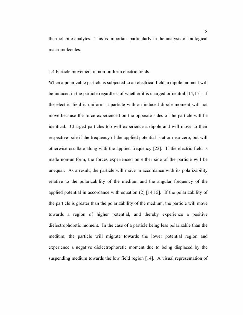
1.4 Particle movement in non-uniform electric fields
When a polarizable particle is subjected to an electrical field, a dipole moment will
be induced in the particle regardless of whether it is charged or neutral [14,15]. If
the electric field is uniform, a particle with an induced dipole moment will not
move because the force experienced on the opposite sides of the particle will be
identical. Charged particles too will experience a dipole and will move to their
respective pole if the frequency of the applied potential is at or near zero, but will
otherwise oscillate along with the applied frequency [22]. If the electric field is
made non-uniform, the forces experienced on either side of the particle will be
unequal. As a result, the particle will move in accordance with its polarizability
relative to the polarizability of the medium and the angular frequency of the
applied potential in accordance with equation (2) [14,15]. If the polarizability of
the particle is greater than the polarizability of the medium, the particle will move
towards a region of higher potential, and thereby experience a positive
dielectrophoretic moment. In the case of a particle being less polarizable than the
medium, the particle will migrate towards the lower potential region and
experience a negative dielectrophoretic moment due to being displaced by the
suspending medium towards the low field region [14]. A visual representation of

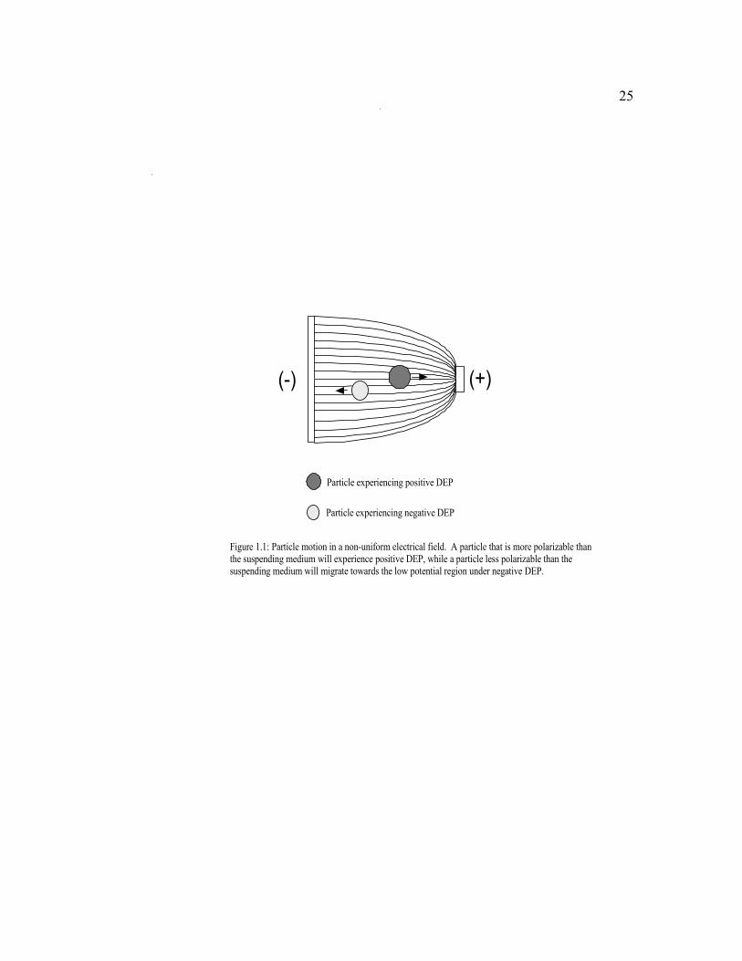
9particles experiencing positive and negative dielectrophoretic moments is shown in
figure 1.1.
Determination of the type of dielectrophoretic moment a particle will experience
can be accomplished by calculating Re[K(ω)] using equation (4). As previously
stated, the real portion of the Clausius-Mossotti factor will dictate whether the
dielectrophoretic force on a particle will be positive or negative. The Clausius-
Mossotti factor is frequency dependent because it is determined from the
frequency dependent complex permittivities of the particle and the medium
[15,16,18]. As such, by constructing a plot of the real component of the Clausius-
Mossotti factor as a function of frequency it is possible to estimate the frequency
ranges in which a particle will exhibit positive DEP and negative DEP. Figure 1.2
is a plot of the real component of the Clausius-Mossotti of Fe3O4 in water.
When an appropriate frequency is applied across the electrodes in a
dielectrophoretic device, a dipole moment is induced in particles in suspension
[14,15]. If the frequency of the applied potential closely correlates to the
relaxation time of the particle, defined as the time required for the induced dipole
to react to the applied field, then the direction of the dipole moment experienced
by the particle will reverse along with the oscillation of the ac voltage. When the
frequency of the ac voltage does not correspond to the relaxation time of the
particle, an induced dipole can still occur but the induced dipole will not be as

10great because the charge density within the particle will not have enough time to
properly accumulate [14]. The influence of directionality of the applied field on
the movement of a particle is not important because if the applied field is reversed
then the direction of the induced dipole moment on a particle will too be reversed
[14,23]. A schematic of this phenomenon is shown in figure 1.3.
It is possible to dictate the type of DEP experienced by a particle through proper
selection of the frequency. Some particles will exhibit positive dielectrophoresis
through a certain frequency range and negative dielectrophoresis in another
frequency range. As shown in figure 1.2, Fe3O4 particles would be expected to
experience positive DEP in the frequency domain up to 1x10¹³ Hz and would be
under negative DEP beyond 1x10¹³ Hz. The frequency at which the direction of
DEP experienced by a particle changes is known as the crossover frequency. At
the crossover frequency the particle will experience no net force [18].
Careful selection of the suspending medium (and more specifically its
conductivity) can be used to increase the selectivity in discriminating between
different analytes as stated in the Clausius-Mossotti factor [17,18,22,24-31]. The
conductivity of the medium can be altered by addition of salts. Ions present in an
aqueous solution create a double layer surrounding a particle and as mentioned by
Pohl [14] will have electrokinetic interactions with the particle. The thickness of

11the double layer can be estimated using the Debye-Hückel screening length
equation [17,32]:
21
228
=
oo
m
eznkT
dπε
(5)
where εm is the permittivity of the medium, k is the Boltzmann constant, T is the
absolute temperature, no is the ion concentration in the bulk of the suspending
medium, z is the valency of the suspending medium, and eo is the charge of an
electron. As shown in equation 5, the thickness of the double layer is inversely
proportional to the concentration of ions present in the suspending medium and is
not dependent on the surface area or volume of the suspended particle. The close
proximity of the double layer to the surface of a particle will contribute to a
particles response to an oscillating electric field through electrokinetic effects
[14,17]. Therefore, it stands to reason that double layer effects on the movement
of a dielectric particle will be more pronounced for small particles in a low ionic
strength medium.
As just stated, the DEP effects experienced by a particle will be affected by the
presence of a double layer, but these added effects are especially noticed when
analyzing submicron particles and macromolecules. This relation can be better
understood by close examination of equation 2. From equation 2, the DEP force

12experienced by a particle is related to the cube of the particle radius. When
dealing with particles where the size is submicron, the contribution of the double
layer thickness will have a more profound impact on the DEP force exerted on a
particle than for particles of micron and larger sizes having similar dielectric
properties because of the relative contribution of the ionic double layer [26,27].
The effects of conductivity of the medium have been studied by several
researchers [24-31]. Green and Morgan observed these behaviors for the study of
latex spheres [24]. Huang and Pethig showed that by altering the conductivity of
the solution and maintaining other conditions constant it was possible to cause a
change in the DEP behavior of yeast cells [25].
1.5 Dielectrophoresis geometries
1.5.1 Parabolic electrodes
Typical devices utilizing parabolic electrodes employ four electrodes to produce a
quadrupole geometry where the electrodes are offset by 90 degrees as shown in
figure 1.4a. Voltage application is accomplished by wiring electrodes diagonally
opposite one another identically [5,34-37]. Once voltage is applied after sample
introduction, particles will begin to collect in regions of high or low potential
depending on the dielectrophoretic moment experienced. In parabolic geometries,
the potential gradient expands radially from the center of the device towards the
electrode surface [24, 33, 34, 38-41].

131.5.2 Castellated electrodes
As shown in figure 4b, castellated electrodes can be configured in two manners:
directly opposite or offset. With either case, the device is wired so that every other
electrode has the same voltage input [5,40,42,43]. In the case of castellated
electrodes that are directly opposite each other, positive and negative
dielectrophoresis regions will be found as follows [40]: Particles focused in the
positive dielectrophoresis region will be found between the faces of the electrodes
located across from each other. Negative dielectrophoresis will congregate
particles in the rectangular areas between the castellations in the electrode.
Positive and negative dielectrophoresis regions for offset castellated electrodes
will be found as follows [40,44]: positive dielectrophoretic particle collection
again occurs in the region between castellated electrodes located across from each
other, the difference being that the positive region is now found between the
corners of the electrode faces. The low potential region for offset castellated
electrodes is identical to that for parallel castellated electrodes (electrodes aligned
directly across from each other) and therefore the negative diectrophoresis region
is located in the rectangular “wells” between electrodes.
1.5.3 Electrode Arrays
Figure 1.4c shows a common electrode array geometry. In devices containing
electrode arrays, voltage applications to the electrodes vary [45,46]. One approach
is to use a checker-board pattern where electrodes having voltage applied and
14those that are grounded are alternated. Another possibility is to have the voltage
vary in concentric squares and to have the voltage vary between ground and
applied voltage with each concentric square. With electrode array geometries, the
high potential region is located on the electrode surface and therefore particles
experiencing a positive dielectrophoretic moment will gather on the electrode
surface. Particles with a negative dielectrophoretic moment aggregate in the low
potential region located in the areas surrounded by four electrodes that form a
square [45,46].
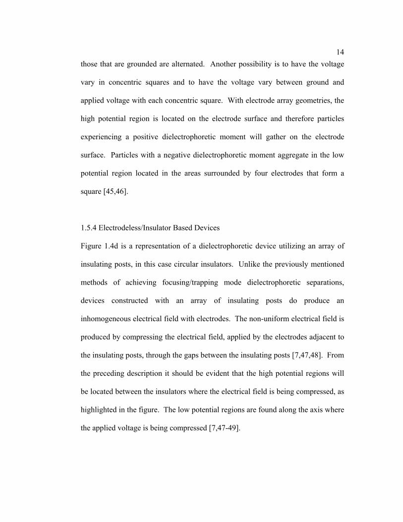
1.5.4 Electrodeless/Insulator Based Devices
Figure 1.4d is a representation of a dielectrophoretic device utilizing an array of
insulating posts, in this case circular insulators. Unlike the previously mentioned
methods of achieving focusing/trapping mode dielectrophoretic separations,
devices constructed with an array of insulating posts do produce an
inhomogeneous electrical field with electrodes. The non-uniform electrical field is
produced by compressing the electrical field, applied by the electrodes adjacent to
the insulating posts, through the gaps between the insulating posts [7,47,48]. From
the preceding description it should be evident that the high potential regions will
be located between the insulators where the electrical field is being compressed, as
highlighted in the figure. The low potential regions are found along the axis where
the applied voltage is being compressed [7,47-49].
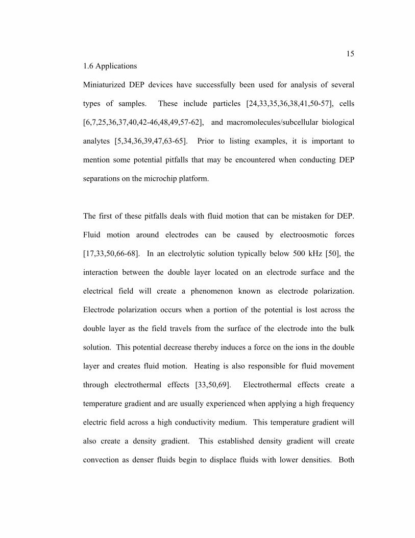
151.6 Applications
Miniaturized DEP devices have successfully been used for analysis of several
types of samples. These include particles [24,33,35,36,38,41,50-57], cells
[6,7,25,36,37,40,42-46,48,49,57-62], and macromolecules/subcellular biological
analytes [5,34,36,39,47,63-65]. Prior to listing examples, it is important to
mention some potential pitfalls that may be encountered when conducting DEP
separations on the microchip platform.
The first of these pitfalls deals with fluid motion that can be mistaken for DEP.
Fluid motion around electrodes can be caused by electroosmotic forces
[17,33,50,66-68]. In an electrolytic solution typically below 500 kHz [50], the
interaction between the double layer located on an electrode surface and the
electrical field will create a phenomenon known as electrode polarization.
Electrode polarization occurs when a portion of the potential is lost across the
double layer as the field travels from the surface of the electrode into the bulk
solution. This potential decrease thereby induces a force on the ions in the double
layer and creates fluid motion. Heating is also responsible for fluid movement
through electrothermal effects [33,50,69]. Electrothermal effects create a
temperature gradient and are usually experienced when applying a high frequency
electric field across a high conductivity medium. This temperature gradient will
also create a density gradient. This established density gradient will create
convection as denser fluids begin to displace fluids with lower densities. Both

16electroosmotic forces and electrothermal effects have the potential to create fluid
motion that may overcome the dielectrophoretic forces being exerted on an
analyte.
Care must be taken when selecting the conductivity of a medium when studying
biological samples. First, if the conductivity of the medium is too high, the
temperature increase may be sufficient to degrade biological analytes. Also, when
dealing with cells care must be taken to make sure an iso-osmotic environment is
established as to not affect the cell wall/membrane [18].
An additional caveat is the production of free radicals through electrochemical
processes [17,70-72]. Free radicals have been shown to produce changes in pH in
dielectrophoretic devices [71], and these pH changes may disrupt the function of
biological analytes. H2O2 has been formed in sugar containing solutions, and the
free radicals are created from the H2O2 decomposition. Catalase has also been
shown to increase the rate of decomposition of H2O2 and in most cases eliminate
H2O2 from the system [72]. Free radicals have too been shown to react directly
with analytes and degrade biological samples [73,74].
The first two examples presented are the works conducted by Green and Morgan
[52], and Watarai et al. [38] and their investigations on the effects on the motion of
submicron latex spheres in a non-uniform electric field. Though these studies do

17not directly demonstrate separations, we feel they must be mentioned because they
are to our knowledge the first examples of the use of DEP forces on submicron
particles. Morgan and Green used castellated electrodes with castellations spaced
at 6 µm and gaps between electrodes measuring 4 µm to study 93 µm diameter
carboxylate modified latex spheres. The applied voltage used was 1 V peak-peak
which produced a field strength of 2.5 x 10⁸ V mm-1. The suspending medium was
pH 7.1 phosphate buffer with a concentration of 1 mM and conductivity of 18 µS
cm-1. Morgan and Green found that for the frequency range of 1 kHz – 1 MHz the
particles exhibited positive DEP and migrated to the electrode tips. The particles
experienced negative DEP for frequencies greater than 20 MHz and collected in
the wells in the electrodes. Watarai, Sakamoto, and Tsukahara too used
microparticles composed of carboxylated polystyrene latex to study the mobility of
these particles due to the dielectrophoretic force. They used a parabolic electrode
device with a quadrupole geometry with a central region of 65 µm. Aqueous
suspensions were made containing (0-5.0) x 10 -3 M KCl and 2.6 x 10⁻⁷ M
Rhodamine B to fluorescently label the spheres. The pH of the solutions were in
the range of 6.08-6.80, and the conductivity of the aqueous solutions were in the
range of 3.11 to 701 µS cm-1 and were adjusted by addition of KCl.
Separation of carboxylate-modified latex spheres on both non-offset and offset
castellated electrodes is shown in figure 1.5 [5]. Electrode distances used were 10
µm. Fluorescently labeled latex spheres of 216 and 557 nm diameters were

18suspended in an aqueous KCl solution with a conductivity of 2.5 µS cm-1.
Separation was accomplished using a voltage of 10 V peak-peak at a frequency of
2 MHz. Upon voltage application, the 216 nm particles collected in the high
potential region located between electrode faces and electrode tips for non-offset
and offset electrodes respectively. The 557 nm diameter particles collected in the
interelectrode gaps under negative DEP. Figure 1.5 is a photograph of the above
mentioned separation of 216 nm and 557 nm carboxylate-modified latex spheres
using a castellated electrode DEP device.
Huang and Pethig [25] used parabolic electrodes to study the effects of varying the
conductivity of the aqueous suspending medium on the type of dielectrophoretic
force on yeast cells. The electrodes were produced from gold and had a thickness
of 70 nm. The 70 nm gold electrodes were laid on a 5 nm thick chromium seed
layer. The final spacing of the electrodes was 64 µm radial opening to the
electrode tips. Suspensions were prepared under two different sets of conditions
for the suspending medium, the first being a suspending medium composed of 280
mM mannitol with a conductivity of 3.61 µS cm-1, and the second prepared with
280 mM mannitol and 1.4 mM KCl and having a conductivity of 170 µS cm-1.
The applied voltage was held constant at 10 V peak-peak and 10 kHz. The
investigators found that yeast cells suspended in 280 mM mannitol experienced
positive DEP, and yeast cells suspended in 280 mM mannitol and 1.4 mM KCl
were focused in the central region between the electrodes.

19
Dielectrophoresis utilizing a castellated geometry has been shown to be a suitable
extraction method for removing cancer cells from blood [58]. Non-offset
castellated gold electrodes with 80 µm electrode spacing were used. A mixture of
MDA 231 breast cancer cells and bovine serum was suspended in an aqueous
solution consisting of 8.5% w/v sucrose and 0.3% w/v dextrose. Hemisodium
EDTA was used to adjust the conductivity of the aqueous solution to 100 µS cm-1.
Upon sample introduction a voltage of 5 V peak-peak at 200 kHz was applied to
trap all cells under positive DEP. A flow of the suspending medium was then
started at 5 µL min-1. The frequency was lowered to 80 kHz to reduce the number
of blood cells trapped on the electrodes. To further purify the breast cancer cells
the frequency was swept between 80 and 20 kHz at a rate of two times per second
for 20 min to free any blood cells that have been trapped on the electrodes by the
cancer cells. At the end of the 20 minute sweeping cycle cell fractions were found
to be >95% pure after the cell fractions were examined using Liu’s modified
Wright staining.
In 1998, another example of separation of cancer cells from blood was
demonstrated using DEP on a 5 x 5 array of electrodes [45]. The array consisted
of circular electrodes composed of a 100 nm Ti-W seed layer covered with a 300
nm thick platinum layer. The electrode diameters were 80 µm and were spaced
200 µm on center. The sample analyzed consisted of epithelial carcinoma cell line

20(HeLa) derived from a human cervical tumor and EDTA-anticoagulated human
blood cells. The separation buffer was composed of 225 nM Tris, 225 nM boric
acid, and 5 nM EDTA, pH 8.2, and 250 mM sucrose. The conductivity of the
separation buffer was measured to be 10 µS cm-1. The separation voltage was 6 V
peak-peak and the frequency was determined empirically. It was discovered that
at 30 kHz the HeLa cells experienced positive DEP and separated from the
peripheral human blood cells which were under a negative dielectrophoretic
moment.
Another dielectrophoretic separation of different cells lines was conducted using
an array of circular electrodes [6]. 25 circular platinum electrodes with diameters
of 80 µm spaced at 200 µm center to center were arranged in a 5x5 geometry. The
electrodes were manufactured as in the previous example and were composed of a
100 nm Ti-W seed layer covered with a 300 nm thick platinum layer. Mixtures of
human glioma cell line (HTB) cells with human neuroblastoma cell line SH-SY5Y
(SH-SY5Y), monocytic cells (U937) with human peripheral blood mononuclear
cells (PBMC), and tax-transformed cells (Ind-2) with PBMC were studied. DEP
buffer was 250 mM sucrose/RPMI 1640, and the final conductivity of the DEP
buffer was 1200 µS cm-1. Voltage was applied in a checkerboard pattern at 7 V
peak-peak and the field frequency varied depending on the cell mixture being
analyzed. Separations occurred in 3-5 minutes after the voltage was applied. Then
cells experiencing negative DEP were flushed from the device at 40 µL min-1 for

2110 min. The voltage was then turned off the and the remainder of cells were
evacuated with DEP buffer at 400 µL min-1 for 20 sec. The frequency of the
applied fields were 400, 500, and 600 kHz for HTB and SH-SY5Y, U937 and
PBMC, and Ind-2 and PBMC mixtures respectively. Cell lines experiencing
positive DEP were HTB, U937, and Ind-2 and were collected on the electrode
surfaces, as shown in figure 1.6a. SH-SY5Y and PBMC were collected under
negative DEP, also shown in figure 1.6a. Photographs of the separation of HTB
and SH-SY5Y, U937 and PBMC, and Ind-2 and PBMC mixtures are shown in
figure 1.6a, and the separation procedure for the U937 and PBMC mixture is
illustrated in figure 1.6b.
Separation of tobacco mosaic virus (TMV) from herpes simplex virus Type 1
(HSV) was demonstrated by Morgan, Hughes, and Green on a polynomial
electrode device [5]. Electrode spacing was 2 µm for interelectrode and 6 µm in
cross center distance. The suspending medium was DI water adjusted to a
conductivity of 100 µS cm-1 using KCl. An applied voltage of 5 V peak-peak at a
frequency of 6 MHz was used to separate TMV from HSV. Under these
conditions TMV experienced positive DEP and collected in the high field regions,
and HSV with a negative dielectrophoretic moment aggregated in the low potential
region. A drawing and photograph of this separation are shown in figure 1.7a and
figure 1.7b respectively.

22An insulator based DEP system was used to separate and concentrate live and dead
E. coli. [7]. The insulators were produced in glass and had a height of 10 µm,
diameter of 200 µm, and were spaced 250 µm on centers. The cells were
suspended in DI water with a conductivity of 22.5 µS cm-1. Direct current voltage
at different voltage levels was used and it was found that at 16 V/mm only live E.
coli. cells were trapped. At a potential gradient of 40 V mm-1 and 60 V mm-1 it
was noticed that both live and dead E. coli. cells were both trapped but formed
distinct bands. The separation of live and dead E. coli at 16 V mm-1, 40 V mm-1,
and 60 V mm-1 are shown in figure 1.8a, 1.8b, and 1.8c respectively.
Another example from the researchers at Sandia National Laboratories using
insulator based DEP is their work on separating live bacteria from water using dc
voltage [48]. The separation device was again constructed of glass with circular
insulators with heights of 10 µm, 150 µm diameters, and distanced 200 µm on
centers. The suspending medium was DI water adjusted to pH 8 with 0.01 N
NaOH and a conductivity of either 22 µS cm-1 with 0.01 M KCl. Results for a
total of six cell mixtures were presented. These cell mixtures were E. coli. (BL21)
and Bacillus subtilis (ATCC #6633), E. coli. (BL21) and Bacillus cereus (ATCC
#14579), E. coli. (BL21) and Bacillus megaterium (ATCC #10778), Bacillus
cereus (ATCC #14579) and Bacillus subtilis (ATCC #6633), Bacillus megaterium
(ATCC #10778) and Bacillus subtilis (ATCC #6633), and Bacillus cereus (ATCC
#14579) and Bacillus megaterium (ATCC #10778). For the mixture containing E.

23coli. and B. subtilis, it was found that with a field of 50 V mm-1 only E. coli was
trapped in the high potential region, and at 75 V mm-1 both E. coli and B. subtilis
were trapped in the higher field region. E. coli. and Bacillus cereus studied at
field strengths of 50 V mm-1 and 75 V mm-1 and in both of these conditions were
not separated. The mixture of E. coli. and Bacillus megaterium was studied at 50
V mm-1 and it was found that only E. coli was trapped and when the field strength
was raised to 90 V mm-1 both E. coli. and Bacillus megaterium were trapped. At a
field of 25 V mm-1 the fourth mixture, Bacillus cereus and Bacillus subtilis, only
B. subtilis was trapped, and at a field of 75 V mm-1 both analytes were retained in
the high field region. Bacillus megaterium and Bacillus subtilis could not be
separated into separate bands at 50 and 75 V mm-1. The final mixture mentioned
was Bacillus cereus and Bacillus megaterium. It was found that at a field strength
of 30 V mm-1 only Bacillus megaterium was trapped and at 75 V mm-1 both
Bacillus cereus and Bacillus megaterium were trapped into separate bands.
As noted in the discussion above, extensive analysis of suspended particles has
been conducted utilizing microfabicated DEP devices. Particle types studied
include but are not limited to: latex spheres, cells, viruses, proteins, and DNA. A
listing of the references from this article, categorized into particle type and device
geometry used in the analysis is given in Table 1.1.
1.7 Conclusions

24Recent advancements in manufacturing have allowed researchers to produce more
effective dielectrophoresis devices than were possible in years past.
Miniaturization has made it possible to conduct separations by applying potentials
of only a few volts. Also, due to the reduction in Joule heating it is possible to
separate particles in the submicron range, which extends the utility of DEP to
biological samples. Current dielectrophoretic devices have been used successfully
for separation of various types of analytes, but depending on the requirements of
the analysis being conducted some geometries will be of greater use than others.
Both conventional dielectrophoresis and unconventional modes of
dielectrophoresis have been gaining popularity as separation tools in the laboratory
and commercially.
25
Figure 1.1: Particle motion in a non-uniform electrical field. A particle that is more polarizable thanthe suspending medium will experience positive DEP, while a particle less polarizable than thesuspending medium will migrate towards the low potential region under negative DEP.
(-) (+)
Particle experiencing positive DEP
Particle experiencing negative DEP

26
-1.0-0.8-0.6-0.4-0.20.00.20.40.60.81.0
Re[
K(ω
)]
109 1010 1011 1012 1013 1014 1015 1016 1017
Frequency (Hz)
Figure 2: Plot of Re[K(ω)] vs. frequency which illustrates the frequency dependence on the polarization of Fe3O4 in 5.62x10⁻² µS cm-1 water.

27
Figure 1.3: Visual depiction showing that particle movement in DEP is not dependent onthe direction of the applied electrical field, as shown for a particle experiencing positiveDEP. For an AC applied waveform, the figure depicts an applied potential at a givenpoint in time.
(-) (+)-+ ----- --
++++
+
++
(+) (-)- +-------
++++
+
++

28
(c)
(a)
+DEP-DEP
Offset electrodes
Non-offset electrodes
(b)
Electrode
Electrode
Insulators
(d)
Figure 1.4: Typical device geometry and regions where positive dielectrophoresis (+DEP) and negativedielectrophoresis (-DEP) are located: (a) polynomial electrode geometry. (b) castellated electrodegeometry showing both non-offset and offset castellated electrodes. (c) an array of circular electrodes.(d) electrodeless geometry where regions of high and low field strength are produced by the compressionof the electric field between the array of insulators.
-DEP
+DEP
+DEP-DEP
+DEP
-DEP

29
Figure 1.5. A video-image capture showing 216 nm and 557 nm diameter latex particles separating on a 10 µm castellated electrode. The red 216 nm spheres experience positive DEP and form pearl chains between opposing electrode tips, while simultaneously the green 557 nm particles experience negative DEP and become trapped in triangular patterns in the interelectrode bays. The applied potential was 10 V peak to peak at a frequency of 2 MHz, and the medium conductivity was 2.5 µS cm-1. Reprinted with permission from [5].

30
Figure 1.6. (A) DEP separation of U937 and PBMC, HTB and SH-SY5Y, and Ind-2 and PBMC in a medium with conductivity of 1200 µS cm-1 at 500, 400, and 600 kHz, respectively. (B) The procedure of DEP separation for U937 and PBMC mixture. B1: Mixture is introduced to the array. B2: U937 cells are separated from PBMC on array by dielectrophoresis 5 min after an ac voltage of 500 kHz, 7 Vpp is applied. U937 cells are collected on the electrodes and PBMC are accumulated at the space between the electrodes. B3: Buffer is introduced from reservoir to the array by fluid flow of 40 µL min-1 while the voltage is kept on. PBMC are carried away with the fluid stream. B4: PBMC are washed off from the array and U937 cells are retained on the electrodes after 10 min of washing. Reprinted with permission from [6].

31
Figure 1.7. A diagram and photograph illustrating the separation of TMV and HSV in a parabolic electrode. The HSV is traped under negative DEP forces at the field minimum in the center of the electrode array, while simultaneously TMV experiences positive DEP and collects at the high-field regions at the electrode edges, resulting in the physical separation of the two particle types. This is illustrated schematically in (a); the photograph appears in (b). The TMV (labeled with rhodamine B) can be seen as a red glow in the arms of the electrodes, and the green/yellow HSV (labeled with NBD-dihexadecylamine) is visible in the center of the electrode. Both viruses were suspended in an electrolyte of conductivity 100 µS cm-1, and the applied potential was 5 V peak to peak at a frequency of 6 MHz. Reprinted with permission from [5].

32
Figure 1.8. Simultaneous concentration and separation of live (green) and dead (red) E. coli by using iDEP. Conductivity of the DI water was 22.5 µS cm-1. Live E. coli cells were at a concentration of 6x10⁷ cells mL-1 and were labled green (Syto 9, Molecular Probes, Eugene, OR). Dead cells were at a concentration of 6 x10⁷ cells mL-1 and labeled red with propidium iodide (red dye, Molecular Probes, Eugene, OR). The circular posts in the arrays are 10-µm deep, 200-µm in diameter, on 250-µm centers, at 0° offset in (a) and (c), and 20° offset in (b). The electric fields applied are (a) 16 V mm-1, only live cells are trapped; (b) 40 V mm-1, differential banding on live and dead cells is observed; and (c) 60 V mm-1, differential trapping of live and dead cells is shown by two separate bands of different color. Live cells (green) are trapped at the wider regions between the circular posts (negative DEP), and dead cells (red) exhibit less negative DEP, since they are trapped at the narrower regions between the circular posts. Reprinted with permission from [7].

33Tables Table 1.1: References for each particle type analyzed and the device geometry utilized.
Particle Type Electrode Geometry Parabolic Castellated Electrode Arrays Electrodeless
Latex Spheres 24, 33, 35, 36, 38, 39, 41, 50, 54, 56 5, 33, 50-53, 57 55
Cells 25, 36, 37, 40, 61 40, 42-44, 57-60 6, 45, 46, 62 7, 48, 49
Macromolecules/subcellular
analytes 5, 34, 36, 39 40, 65 63 47, 49, 64

34
References
[1] H. Pohl, J. Appl. Phys. 22 (1951) 869
[2] H.A. Pohl, C.E. Plymale, J Electrochem Soc. 107 (1960) 390
[3] T.B. Jones, IEE Proc.-Nanobiotechnol. 150 (2003) 39
[4] A.S. Bahaj, A.G. Bailey, Proc. of IEEE/IAS Annual Meeting. (1979) 154
[5] H. Morgan, M.P. Hughes, N.G. Green, Biophys, J. 77 (1999) 516
[6] Y. Huang, S. Joo, M. Duhon, M. Heller, B. Wallace, X. Xu, Anal. Chem. 74
(2002) 3362
[7] B.H. Lapizco-Encinas, B.A. Simmons, E.B. Cummings, Y. Fintschenko, Anal.
Chem. 76 (2004) 1571
[8] Y. Li, K.V.I.S. Kaler, Anal. Chim. Acta. 507 (2004) 151
[9] X.-B. Wang, M.P. Hughes, Y. Huang, F.F. Becker, P.R.C. Gascoyne, Bichim.
Biophys. Acta 1243 (1995) 185
[10] H. Morgan, N.G. Green, M.P. Hughes, W. Monaghan, T.C. Tan, J.
Micromech. Microeng. 7 (1997) 65
[11] H. Morgan, A.G. Izquierdo, D. Bakewell, N.G. Green, A. Ramos, J. Phys. D:
Appl. Phys. 34 (2001) 1553
[12] X.-B. Wang, J. Yang, Y. Huang, J. Vykoukal, F.F. Becker, P.R.C. Gascoyne,
Anal. Chem. 72 (2000) 832
[13] A.I.K. Lao, Y.-K. Lee, I.-M. Hsing, Anal. Chem. 76 (2004) 2719
[14] H. Pohl, Dielectrophoresis: The Behavior of Neutral Matter in Nonuniform
Electric Fields. Cambridge University Press, New York, NY, 1978

35
[15] T.B. Jones, Electromechanics of Particles, Cambridge University Press, New
York, NY, 1995
[16] L. Benguigui, I.J. Lin, J. Appl. Phys. 53 (1982) 1141
[17] P.R.C. Gascoyne, J. Vykoukal, Electrophoresis. 23 (2002) 1973
[18] M.P. Hughes, Electrophoresis. 23 (2002) 2569
[19] X. Wang, X.-B. Wang, P.R.C. Gascoyne, J. Electrostat. 39 (1997) 277
[20] M. Washizu, T.B. Jones, J. Electrostat. 38 (1996) 199
[21] T.B. Jones, M. Washizu, J. Electrostat. 37(1996) 121
[22] A.D. Goater, R. Pethig, Parasitology. 117 (1998) S177
[23] R. Hölzel, F.F. Bier, IEE Proc.-Nanobiotechnol. 150 (2003) 47
[24] N.G. Green, H. Morgan, J. Phys. D: Appl. Phys. 30 (1997) 2626
[25] Y. Huang, R. Pethig, Meas. Sci. Technol. 2 (1991) 1142
[26] W.M. Arnold, H.P. Schwan, U. Zimmermann, J. Phys. Chem. 91 (1987) 5093
[27] N.G. Green, H. Morgan, J. Phys. Chem. B. 103 (1999) 41
[28] Y. Huang, X.-B. Wang, R. Hölzel, F.F. Becker, P.R.C. Gascoyne, Phys. Med.
Biol. 40 (1995) 1789
[29] Y. Huang, X.-B. Wang, F.F. Becker, P.R.C. Gascoyne, Biochim. Biophys.
Acta 1282 (1996) 76
[30] V.L. Sukhorukov, W.M. Arnold, U. Zimmermann, J. Membrane Biol. 132
(1993) 27
[31] X.-B. Wang, Y. Huang, P.R.C. Gascoyne, F.F. Becker, R. Hölzel, R. Pethig,
Biochim. Biophys. Acta 1193 (1994) 330

36
[32] J.O’M. Bockris. Modern Electrochemistry Vol. 2. Plenum Press. New York,
NY, 1972, p. 730
[33] N.G. Green, A. Ramos, H. Morgan, J. Phys. D: Appl. Phys. 33 (2000) 632
[34] S. Asokan, L. Jawerth, R.L. Carroll, R.E. Cheney, S. Washburn, R. Superfine,
Nano Lett. 3 (2003) 431
[35] S. Tsukahara, T. Sakamoto, H. Watarai, Langmuir 16 (2000) 3866
[36] S. Tsukahara, H. Watarai, IEE Proc.-Nanobiotechnol. 150 (2003) 59
[37] K. Ratanachoo, P.R.C. Gascoyne, M. Ruchirawat, Biochim. Biophys. Acta
1564 (2002) 449
[38] H. Watarai, T. Sakamoto, S. Tsukahara, Langmuir 13 (1997) 2417
[39] M.P. Hughes, H. Morgan, J. Phys. D: Appl. Phys. 31 (1998) 2205
[40] X.-B. Wang, Y. Huang, J.P.H. Burt, G.H. Markx, R. Pethig, J. Phys. D: Appl.
Phys. 26 (1993) 1278
[41] T. Müller, A. Gerardino, T. Schnelle, S.G. Shirley, F. Bordoni, B.D. Gasperis,
R. Leoni, G. Fuhr, J. Phys. D: Appl. Phys. (1996) 340
[42] P.R.C. Gascoyne, J. Noshari, F.F. Becker, R. Pethig, IEEE T. Ind. Appl. 30
(1994) 829
[43] P. Gascoyne, C. Mahidol, M. Ruchirawat, J. Satayavivad, P. Watcharasit, F.F.
Becker, Lab Chip 2 (2002) 70
[44] R. Pethig, Y. Huang, X.-B. Wang, J.P.H. Burt, J. Phys. D: Appl. Phys. 24
(1992) 881

37
[45] J. Cheng, E.L. Sheldon, L. Wu, M.J. Heller, J.P. O’Connell, Anal. Chem. 70
(1998) 2321
[46] J. Cheng, E.L. Sheldon, L. Wu, A. Uribe, L. O. Gerrue, J. Carrino, M.J.
Heller, J.P. O’Connell, Nat. Biotechnol. 16 (1998) 541
[47] C-F Chou, J.O. Tegenfeldt, O. Bakajin, S.S. Chan, E.C. Cox, N. Darnton, T.
Duke, R.H. Austin, Biophys. J. 83 (2002) 2170
[48] B.H. Lapizco-Encinas, B.A. Simmons, E.B. Cummings, Y. Fintschenko,
Electrophoresis 25 (2004) 1695
[49] C-F Chou, F. Zenhausern, IEEE Eng. Med. Biol. 22 (2003) 62
[50] A. Ramos, H. Morgan. N.G. Green, A. Castellanos, J. Phys. D: Appl. Phys.
31 (1998) 2338
[51] N.G. Green, H. Morgan, J. Phys. D: Appl. Phys. 31 (1998) L25
[52] N.G. Green, H Morgan, J. Phys. D: Apply. Phys. 30 (1997) L41
[53] M.P. Hughes, H. Morgan, Anal. Chem.71 (1999) 3441
[54] M. Abe, M. Orita, H. Yamazaki, S. Tsukamoto, Y. Teshima, T. Sakai, T.
Ohkubo, N. Momozawa, H. Sakai, Langmuir, 20 (2004) 5046
[55] E.B. Cummings, A.K. Singh, Anal. Chem. 75 (2003) 4724
[56] A. Docoslis, P. Alexandridis, Electrophoresis 23 (2002) 2174
[57] R. Casanella, J. Samitier, A. Errachid, C. Madrid, S. Paytubi, A. Juárez, IEE
Proc.-Nanobiotechnol. 150 (2003) 70
[58] F.F. Becker, X.-B. Wang, Y. Huang, R. Pethig, J. Vykoukal, P.R.C.
Gascoyne, Proc. Natl. Acad. Sci. 92 (1995) 860

38
[59] X.-B. Wang, Y. Huang, P.R.C. Gascoyne, F.F. Becker, IEEE T. Ind. Appl. 33
(1997) 660
[60] P.R.C. Gascoyne, X.-B. Wang, Y. Huang, F.F. Becker, IEEE T. Ind. Appl. 33
(1997) 670 [61] I. Ikeda, S. Tsukahara, H. Watarai, Anal. Sci. 19 (2003) 27
[62] Y. Huang, K.L. Ewalt, M. Tirado, R. Haigis, A. Forster, D. Ackley, M.J.
Heller, J.P. O’Connell, M. Krihak, Anal. Chem. 73 (2001) 1549
[63] R.G. Sosnowski, E. Tu, W.F. Butler, J.P. O’Connell, M.J. Heller, Proc. Natl.
Acad. Sci. 94 (1997) 1119
[64] J.O. Tegenfeldt, C. Prinz, H. Cao, R.L. Huang, R.H. Austin, S.Y. Chou, E.C.
Cox, J.C. Sturm, Anal. Bioanal. Chem. 378 (2004) 1678
[65] W.A. Germishuizen, C. Wälti, P. Tosch, R. Wirtz, M. Pepper, A.G. Davies,
A.P.J. Middelberg, IEE Proc-Nanobiotechnol. 150 (2003) 54
[66] N.G. Green, A. Ramos, A. González, H. Morgan, A. Castellanos, Phys. Rev.
E 61 ( 2000) 4011
[67] A. González, A. Ramos, N.G. Green, A. Castellanos, H. Morgan, Phys. Rev.
E 61 (2000) 4019
[68] N.G Green, A. Ramos, A. González, H. Morgan, A. Castellanos, Phys. Rev. E
66 (2002) 026305-1
[69] B. Malyan, W. Balachandran, J. Electrostat. 51-52 (2001) 15
[70] R.S. Nicholson, I. Shain, Anal. Chem. 37 (1965) 190

39
[71] G. Fuhr, T. Müller, T. Schnelle, R. Hagedorn, A. Voigt, S. Fiedler W.M.
Arnold, U. Zimmermann, B. Wagner, A. Heuberger, Naturwissenschaften 81
(1994) 528
[72] X. Wang, J. Yang, P.R.C. Gascoyne, Biochim. Biophys. Acta 1426 (1999) 53
[73] C-Y Hsu, C-M Yang, C-M Chen, P-Y Chao, S-P Hu, J. Agric. Food Chem.
563 (2005) 2746
[74] R.C. Murphy, Chem. Res. Toxicol. 14 (2001) 463

40
Chapter 2:
Dielectrophoretic Ratchet Devices

41
2.1 Introduction
Chapter 1 detailed the fact that semiconductor manufacturing technology has been
successfully implemented in the manufacture of miniaturized dielectrophoretic
devices. Benefits of device miniaturization include tighter electrode spacing,
lower applied potentials to create high field gradients, decreased consumption of
reagents and sample, reduced analysis time, possibility of portable
instrumentation, and lower limits of detection.
Currently, miniaturized devices are being coupled to one another to produce micro
total analysis systems (µTAS) [1-4]. In the case of dielectrophoresis,
dielectrophoretic components have been successfully coupled with mixers,
electrophoresis chips, electrorotation systems, and field deployable devices. The
different miniaturized components used in a µTAS device can be selected for a
specific sample and can be built to incorporate sample preconcentration,
separation, and detection units on a single integrated device. µTAS devices can
reduce the chance of human error, such as mislabeling and contamination, by
decreasing the number of times a sample is handled, in the process generating the
required measurements.

42Several dielectrophoretic device geometries have been successfully fabricated and
utilized for selective collection of a wide range of suspended analytes. Though
utilization of semiconductor technology has been shown to be beneficial for
miniaturizing devices, one device geometry that has seen limited use in the field of
dielectrophoresis is ratchet devices. Presented in this chapter, is a brief overview
of current ratchet dielectrophoretic devices, and also described is a ratchet type
dielectrophoretic device constructed and used for the research efforts of this
dissertation.
2..2 Ratchet Devices
The ratchet concept was originally described by Pierre Curie to describe how
motion can be limited to one direction, and was later revisited by Richard
Feynman who described how in theory an item could be lifted without any energy
input [5,6]. Building upon the ideas presented by Curie and Feynman, Chauwin,
Ajdari and Prost then applied the concept of ratchets to show that Brownian
motion can be controlled to the extent that selective particle movement can be
attained [7].
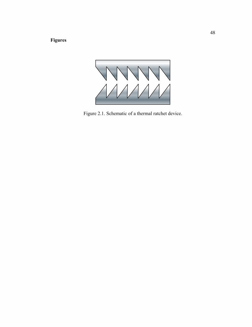
Later, Rousselet et al. showed that Brownian motion and dielectrophoretic
phenomena could be used in combination to “selectively” move latex particles in a
single direction, and as such, these devices were labeled thermal ratchets [8]. The
device consisted of a photolithographicaly produced interdigitated electrode

43geometry in which the electrode edges resembled “Christmas tree” shapes. A
schematic representation of a “Christmas tree” portion of the device is shown in
Figure 2.1. In this device, particles experiencing positive dielectrophoresis are
collected at the electrode tips and particles under negative dielectrophoresis were
found to collect, through empirical observations, in a crescent-shaped region near
the widest distance between respective electrode sets, as shown in figure 2.2.
Particle movement was attained by first collecting particles at the electrode tips
under positive dielectrophoresis. Once the particles collected, the electrodes were
de-energized and the particles were allowed to diffuse. During the diffusion
process, a portion of the particles collected at the previously energized electrode
tip diffused into the subsequent (2nd) ratchet portion. Then by reenergizing the
electrodes, the particles in the 2nd ratchet portion were collected at the electrode tip
located downstream of the first electrode tip. The process was repeated until the
particles moved down the ratchet.
2.3 Stacked Ratchets Device
Building upon the thermal ratchet work conducted by Rousselet et al., Gorre-Talini
et al. developed a stacked ratchet device and implemented it in the movement of
0.5 µm latex spheres [9]. Unlike the thermal ratchet device, which depends on
Brownian motion to move particles into successive ratchet sets, particle movement
in the stacked ratchet geometry depends solely on dielectrophoretic manipulation.

44Figure 2.3 is an illustration of a stacked ratchet device and is composed of two sets
of “Christmas tree” shaped electrodes that are stacked on top of one another.
The device was operated as follows, and is illustrated in figure 2.4. After sample
introduction, power was applied to the first set of electrodes, the gold electrodes in
figure 2.4. Once particles had collected in the positive dielectrophoretic region as
shown in figure 2.4b, power to the first electrode set was turned off. Power was
then applied to the second electrode set and particles experiencing a positive
dielectrophoretic moment moved to the tips of the second electrode pair, figure
2.4c. By altering the power application between the sets of electrodes, latex
particles were transported towards the opposite end of the device. To date only
movement of particles experiencing positive dielectrophoresis has been
accomplished7, and no successful separation has been conducted utilizing this
electrode geometry. No separation has been demonstrated because thermal motion
caused by electrode heating countered the dielectrophoretic force exerted on a
particle.
2.4 Proposed Ratchet Type Device
From the preceding, it can be seen that dielectrophoretic ratchet devices offer the
possibility to induce particle movement though a device by combining Brownian
motion and dielectrophoresis (thermal ratchets) or solely dielectrophoretic forces

45(stacked ratchets). Though ratchet geometries offer an interesting avenue for
particle movement without the use of any external flow, no separations to date
have been conducted. Also, no investigations have been made into device
optimization through modification of the required electrodes. The following is a
description of a proposed design of a ratchet type dielectrophoretic device.
One possibility in modifying the electrode features is shown in figure 2.5a. In this
device, the two sets of Christmas tree shaped electrodes are replaced with
electrode pairs in a V shaped geometry. These electrode features can be
constructed using LIGA (Lithographie Galvanformung Abformung, German for:
Lithography Electroplating Molding) technology to produce electroformed nickel
electrodes.
To produce the fluidic component for this device a PDMS cover layer can be
employed, and can be constructed to configure the device as either a flow through
or static system. For the flow through system, the PDMS component will be
constructed with a “Christmas tree” shaped channel which will serve two
functions, as shown in figure 2.5b. The first purpose is to create the separation
channel, and secondly to cover the top of the electrodes, thereby reducing the total
electrode surface area that is in contact with solution, thus reducing thermal
motion. A second benefit created by capping the electrode features with a PDMS
cover layer is that the vertical sidewalls of the dielectrophoretic device are

46composed of electrodes which will ensure that all particles located within the
device are subjected to the induced dielectrophoretic force. For the static
geometry, the PDMS cover layer contains the same features as the flow through
geometry, and differs in only two respects. First, the static PDMS fluidic
component will not contain the fluidic connections because a well will be placed
around the ratchet type components. Secondly, since a sample aliquot will be
pipetted directly into the reservoir, a microscope cover slip will be used to cover
the well to reduce evaporation of the suspending medium.
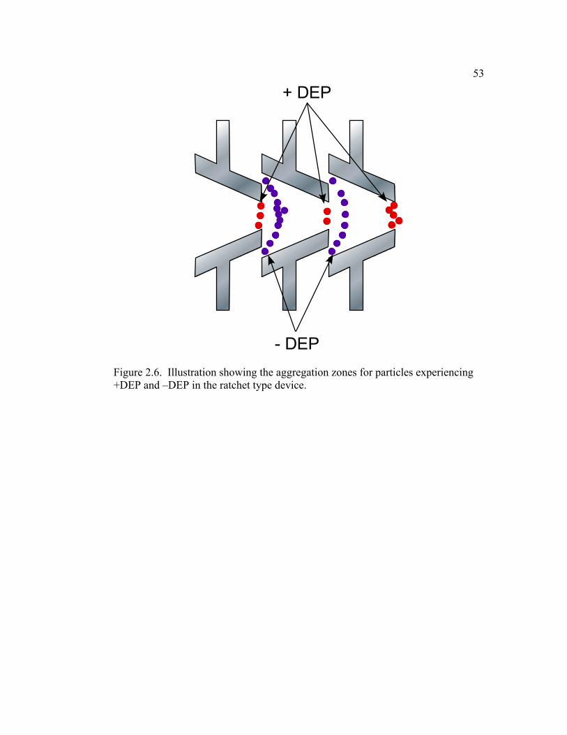
This device can be operated in a similar fashion to a ratchet geometry device.
Upon energizing the electrodes, particles experiencing +DEP will collect at the
electrode tips, and particles experiencing –DEP will also collect in a crescent-
shaped line along the widest regions of the ratchet types, shown in chapters 4 and
5 of this dissertation. Figure 2.6 illustrates the aggregation regions for particles
experiencing +DEP and –DEP. When attempting to operate the device as a
stacked ratchets device, the sets of electrodes can be divided into two groups as
shown in figures 2.5a and 2.5c. Each of the two groups of electrodes will be
connected to the same function generator, and through the use of an on/on switch
the electrodes can be divided into the two separate groups.
Possible applications of the proposed dielectrophoretic device are as follows. The
first possible application of this device is for sorting of biological samples such as

47benign and malignant cells, live and dead viruses, and isolation of blood serum
components. A second application is as a sample cleanup component of a µTAS
to collect and concentrate analytes prior to subsequent analysis. For this current
work, the process taken in fabricating this device (chapters 3 and 4) and the initial
evaluation of this device by collection of particles based on the dielectric
properties of the test analytes (chapter 4 and 5) are presented.
48Figures
Figure 2.1. Schematic of a thermal ratchet device.

49
Figure 2.2. Illustration showing regions of particle collection during application of an electric field across the electrode set. Particles collected at the bottle necks under +DEP, and aggregate along the crescent-shaped line is region of particle aggregation under –DEP.

50
Figure 2.3. Schematic of a stacked ratchets device.

51
(a)
(b)
(c)
Figure 2.4. Illustration of a stacked ratchets device functioning over a single cycle of operation. (a) Sample is introduced into the device and is randomly distributed. (b) Lower electrode set is energized and particles collect under +DEP. (c) Upper electrode set is then energized and particles migrate under +DEP to the following ratchet tip.

52
Figure 2.5. Schematic of the parts necessary for constructing a ratchet type device. (a) Glass slide containing the electroformed electrodes. (b) PDMS layer housing fluidic components. (c) Device assembled and each group of electrodes connected to their respective terminals of an on/on switch.
53
+ DEP
- DEP
Figure 2.6. Illustration showing the aggregation zones for particles experiencing +DEP and –DEP in the ratchet type device.

54References [1] D.R. Reyes, D. Iossifidis, P.A. Auroux, A. Manz, Anal. Chem 74 (2002)
2623–2636.
[2] P.A. Auroux, D. Iossifidis, D.R. Reyes, A. Manz, Anal. Chem 74 (2002)
2637–2652.
[3] T. Vilkner, D. Janasek, A. Manz, Anal. Chem 76 (2004) 3373.
[4] P.S. Dittrich, K. Tachikawa, A. Manz, Analytical Chemistry 78 (2006)
3887.
[5] P. Curie, French) Journal de Physique, 3, III, 393-415 (1894).
[6] R.P. Feynman, R.B. Leighton, M. Sands, The Feynman lectures on
physics, Addison-Wesley Redwood City, Calif, 1963.
[7] J.F. Chauwin, A. Ajdari, J. Prost, Europhysics letters(Print) 27 (1994) 421.
[8] J. Rousselet, L. Salome, A. Ajdari, J. Prostt, Nature 370 (1994) 446.
[9] L. Gorre-Talini, J.P. Spatz, P. Silberzan, Chaos 8 (1998) 650.
55
Chapter 3:
Use of Dupont MX-5000 Series Dry Film Photoresist for
Fabrication of Soft Lithography Masters
Carlos F. Gonzalez, Corey R. Koch, Vincent T. Remcho
Submitted to Lab on a Chip Royal Society of Chemistry, Thomas Graham House, Science Park
Milton Road, Cambridge CB4 0WF, UK

56Abstract
Presented is a method for production of negative image masters for soft
lithography replica molding using Dupont MX-5000 series microlithographic dry
film photoresist. Factors studied include substrate suitability, appropriate exposure
source, exposure source effects on feature size, and maximum height to width
aspect ratio attainable. Masters studied were constructed from a single resist layer.
Master performance was tested through replica molding to produce
poly(dimethylsiloxane) components containing a negative image of the
lithographic features contained on the master.
3.1 Introduction
Soft lithographic production of poly(dimethylsiloxane) (PDMS) components has
become common practice in the construction of microfluidic devices, and a key
step in the patterning of PDMS is the manufacture of suitable masters. Currently,
masters used for replica molding of PDMS are made by etching silicon wafers [1]
or glass slides [2], patterning printed circuit boards [3], creating resist features
from liquid photoresists such as SU-8 [4], solid object printing [5], embossing
acrylic masters from machined aluminum wafers [6], and casting and curing of
polyester resin in a PDMS mold patterned using an SU-8 master containing
negative features of the final PDMS component [7]. Another interesting
possibility for a producing master for use in replica molding of PDMS

57microfluidic device components is the use of dry film resist, which has seen
limited use in microfluidics.
Some of the first uses of dry film resist in microfluidics were for the construction
of resist-glass hybrid devices [8-11]. Negative image masters patterned with dry
film resist have been shown to be suitable molds for producing hot embossed
microfluidic device components [12]. The possibility of masters manufactured
from dry film resist for patterning of PDMS has been discussed [9], and to the best
of our knowledge, there have been no examples of replica molded PDMS
components using negative image dry film resist masters presented in the
literature. Here, we describe a method by which Dupont MX-5000 series dry film
photoresist is used for the construction of masters for replica molding.
The MX-5000 series resist is a negative tone resist and is processed similarly to
other negative resists, while exhibiting differences that make it an intriguing
alternative. First, this resist is a dry film that is laminated onto a substrate and not
spun on like a liquid photoresist, thereby eliminating the need for a spin coater.
Also, eliminated are resist edge beads and other non-uniformities common with
spin coating liquid photoresist. The resist is supplied as sheets or on a roll, and in
either case the resist is sandwiched between a polyethylene layer and polyester
layer. The polyethylene layer is removed prior to lamination, and then the resist is
laminated onto the substrate by rolling and pressing to the substrate surface. The

58polyester layer is retained throughout the exposure procedure in order to keep the
photomask clear of the resist.
The MX5000 series exhibits maximum absorption at 365 nm, and exposure is
accomplished through the use of a UV exposure system containing the 365 nm
mercury i-line. Due to this quality, the resist can be exposed using a conventional
UV lithographic exposure system, while offering the possibility of using other less
costly systems. Upon exposure, the resist turns from green to dark blue thereby
making the features visible, and this characteristic also allows for the assurance of
an adequate exposure dosage. Per the Dupont technical data, care must be taken to
minimize exposing the resist to light up to 450 nm due to undesired resist
crosslinking that may lead to loss of feature resolution.
Another key feature of the resist is the developing and rinsing solutions used.
With many photoresists in current use, development and rinsing is accomplished
with organic solvents. For the MX-5000 series resist, development is conducted
with a potassium carbonate solution, and the rinse employed is water with a 300
ppm calcium carbonate hardness. This feature is of particular interest because
disposal of waste organic developer and rinsing solutions is eliminated.
Development can be accomplished outside of a fume hood due to the lack of
organic vapors.

593.2 Experimental
3.2.1 Reagents and Materials
Technical grade acetone and methanol were used for substrate cleaning (Northwest
Solvents, Eugene, OR). Ultrapure water used for substrate cleaning and
developer/rinsing solution preparation was obtained from a Barnstead E-Pure
system (Dubuque, IA). Dupont D-4000 IC concentrated developer, used for
preparation of the developing solution,n was purchased from Microchem (Newton,
MA). Technical grade calcium carbonate (Fischer Scientific, Pittsburgh, PA) was
used for preparation of the rinsing solution. 2 x 3 inch borosilicate glass slides
used as master substrates were purchased from VWR (West Chester, PA). 3 inch
mechanical grade silicon wafers also used for master substrates were purchased
from University Wafers (South Boston, MA). Dupont MX-5000 photoresist for
patterning was purchased from Microchem (Newton, MA). Dry film resist
thicknesses of 20 µm (MX-5020) and 50 µm (MX-5050) were used. Mylar
photomasks were designed using AutoCAD 2007 (Autodesk, San Rafael, CA) and
were photoplotted by CAD/Art Services, Inc. (Bandon, OR).
3.2.2 Equipment
For descumming the substrate surface, a home-built oxygen plasma was used. The
plasma system consists of an MDC Vacuum Products Corporation (Hayward, CA)
6 inch x 10 inch 4-port stainless steel vacuum chamber, and an XEI Scientific
(Redwood City, CA) Evactron Decontaminator RF Plasma Cleaner. A homemade

60rolling pin for laminating substrates with photoresist was constructed by inserting
a glass rod into a piece of rubber tubing. A 3M rubber squeegee for smoothing
the resist was purchased from an automotive paint supply shop. Quarter inch
aluminum plates used for promoting adhesion between the resist and substrate
were purchased from McMaster-Carr (Los Angeles, CA). The four exposure
sources tested were a homemade UV flood exposure system consisting of an Oriel
6186 mercury arc lamp (Oriel Light Sources and Spectroscopy Instrumentation,
Stratford, CT) and a Durst 606 photo enlarger (purchased used, locally) to direct
the UV light at a right angle towards the substrate, a Spectroline X-15A longwave
365 i-line light source (Spectronics Corporation, Westbury, NY), an MG
Chemicals (Surrey, B.C., Canada) fluorescent light, and a Kepro BTX-200 Ultra
Violet Exposure Frame (Fenton, MO) which was donated by our electronics shop.
A Paschee VLS airbrush (Chicago, IL) was used for resist development. For
imaging a Leica Wild Stereozoom microscope (Wetzlar, Germany) fitted with a
Sony Power HAD DXC-970MD camera (Sony Corporation, New York, NY) and
ImagePro Plus 6.0 software (MediaCybernetics, Silver Spring, MD) was utilized.
A Zeiss Axiotron (Carl Zeiss MicroImaging, Inc., Thornwood, NY) equipped with
a Sony Power HAD DXC-970MD camera (Sony Corporation, New York, NY) and
ImagePro Plus 6.0 (MediaCybernetics, Silver Spring, MD) was used to image and
measure resist feature widths. To measure resist thickness and to map surfaces, a
Veeco Dektak 8 Stylus Profiler with a 12.5 µm tip (Veeco Instruments Inc.,
Woodbury, NY) was employed.
61
3.2.3 Factors Studied
Several factors were studied in determining if Dupont MX-5000 microlithographic
dry film photoresist is well suited for constructing masters intended for soft
lithographic replica molding. These items include: exposure sources, selection of
a substrate that provides sufficient adhesion with the resist, exposure source effects
on feature size and maximum height to width aspect ratio attainable, master
production, and performace of each master type.
3.2.3.1 Exposure Sources
Our first focus was on finding a suitable exposure source capable of crosslinking
the resist. For this particular resist, an appropriate exposure source is one which
will cause the resist to change color from green to dark blue. In this portion of the
experiment, borosilicate glass slides were laminated with a single layer of resist,
either MX-5020 or MX-5050, as described below. The laminated slides were
cleaned, exposed, and patterned with a photomask containing five straight lines of
different widths (25 µm, 50 µm, 100 µm, 150 µm, and 200 µm) by 3 cm long for
increasing amounts of time to determine the minimum amount of time required for
one of the four previously described exposure sources to provide a sufficient
exposure dosage.
3.2.3.2 Resist Adhesion
62Using the exposure systems that adequately exposed the resist, the next factor
evaluated substrate efficacy in providing sufficient adhesion to the resist. For this,
borosilicate glass slides and silicon wafers were examined for suitability, and
again a single layer of MX-5020 and MX-5050 was laminated onto either a wafer
or slide. The slides were again patterned with the straight line feature mask
described above, and were then processed as described in the single layer master
production section.
3.2.3.3 Exposure Source Effects on Feature Size and Maximum Aspect Ratio
In this section of the study, the straight line resist patterned substrates produced to
test the adhesion of the resist to the substrate were used. A representative example
of each resist thickness produced using the light sources found to be appropriate
was employed. These masters were then used to determine if the line widths
produced varied with exposure source. Then the maximum height to width aspect
ratio was determined for both the MX-5020 and MX-5050 resist. The maximum
aspect ratios were ascertained using the linear lithographic feature with the
smallest width that was successfully produced.
To measure the line widths, the previously described Zeiss AxioTron microscope
equipped with ImagePRO Plus 6.0 video capture image software was used. The
lines were measured randomly at five locations. From these measurements, the

63average line width was determined. The calculated averages were then used to see
if the exposure source yielded the expected line width.
In determining the maximum attainable height to width aspect ratio, a Veeco
Dektak 8 Stylus Profiler was employed to measure the resist height. Five
measurements of the resist height for the linear features with the smallest width
were taken to find an average resist height. The maximum height to width aspect
ratio was then determined using the average resist height and widths calculated.
3.2.3.4 Single Resist Layer Masters
After determining which substrate provided the best adhesion, single layered
masters were patterned and produced to contain features for a microchip: a double-
tee capillary electrophoresis device. The feature dimensions of the double-tee
photomask were as follows: 1 cm long sample and sample waste side arms, 4.25
cm total main channel length with an injection length of 2.5 mm and a separation
length of 3 cm, and for all features mentioned, the line widths were 100 µm.
These masters were produced as described in the single layer master production.
3.2.3.5 Master Performance
To test the performance of the masters, replica molding of PDMS was conducted
using the single layer, multilayer resist, and multidimensional resist masters.

64PDMS was mixed in a 10:1 oligimer to curing agent ratio. Following mixing, gas
bubbles were removed by placing the PDMS mixture in a vacuum desiccator and
applying vacuum. The degassed PDMS was then poured over the master. The
assembly was then placed in a 95 °C oven for 1 hr to cure the PDMS. The cured
PDMS was then peeled from the master after the assembly was removed from the
oven and was allowed to cool to room temperature.
Once at room temperature, the cured PDMS was removed from the master. The
master and PDMS were then examined to see if there were any resist adhesion
issues. The first issue examined was adhesion failure between the resist and
master surface. Also studied was loss of interlayer resist adhesion for the masters
fabricated with multiple resist layers. If resist was present in the PDMS features,
the corresponding region of the master was examined with a microscope to
determine the extent to which the resist was removed from the substrate surface. If
resist was absent in these regions, it was taken as an indication that there was an
adhesion issue between the resist and substrate. Also, all of the masters were
inspected to determine if there was delamination between the resist and substrate
surface. For the multilayer and multidimensional masters interlayer resist
separation was too scouted for by eye and with a microscope.
3.2.4 Methods Used for Producing Masters
3.2.4.1 Substrate Cleaning

65Substrate cleaning was conducted as follows. The glass slides were rinsed with
acetone, methanol, and ultra pure water. Following the rinse, the substrates were
dried with a stream of nitrogen gas. To ensure the substrate surface was free of
any residual organic contaminants, the surface was descumed in an oxygen
plasma. The oxygen plasma parameters used were a chamber pressure of 200
mTorr and a power setting of 22 W. The total time the substrate was exposed to
the oxygen plasma was in the range of 2-3 min. For the silicon wafers, the
cleaning process consisted of rinsing the substrate surface with ultra pure water,
drying under a stream of nitrogen gas, and descuming the substrate surface in an
oxygen plasma. The plasma parameters used for cleaning the silicon wafers was
identical to that of the glass slides.
3.2.4.2 Single Layer Master Production
Resist lamination was carried out as follows. First, the polyethylene layer was
removed from the resist. The resist was then laminated onto the substrate by
employing the homemade rolling pin. The laminated substrate was then placed on
an aluminum plate at 95 °C. The laminated substrate was allowed to warm and
any imperfections present were removed using a rubber squeegee. A second
aluminum plate at 95 °C was then placed on top of the laminated for 30 s. The
laminated substrate was then subjected to a post lamination bake of 20 min in a 65
°C oven, to improve adhesion between the resist and substrate surface. After the
66post lamination bake, the laminated substrate was allowed to cool to room
temperature in a dark drawer.
The laminated substrate was then masked using a Mylar photomask, and to ensure
the photomask was in direct contact with the resist it was weighted down using a
glass slide. Exposure was accomplished using one of the four exposure sources
previously described. The exposure times for the mercury arc lamp system and
Spectraline light source was 2 min, and for the MG Chemicals and Kepro sources
exposure times up to 1 hr were examined. The exposed laminated substrate was
post exposure baked at 100 °C for 25 min on a hot plate.
Prior to developing, the polyester layer was removed from the resist. The resist
was then developed using an aqueous 0.75 vol. % D-4000 IC concentrated
developer solution and rinsed using an aqueous 300 ppm carbonate solution. Both
the diluted developer solution and rinsing solution were heated in a water bath to
45 °C. The developer was sprayed onto the resist using an air brush operated at 20
psi of nitrogen gas, or as otherwise stated. The rinsing solution was sprayed onto
the substrate using a plastic spray bottle. The rinsing/developing stages were
carried out as follows. Working from the edge of the substrate towards the center,
a small area of the substrate was developed, and then immediately rinsed. After
the 300 ppm final calcium carbonate rinse, the master was rinsed with ultra pure

67water, and then dried with a stream of nitrogen gas. The dried master was then
baked on a 100 °C hot plate for 25 min.
3.3 Results and Discussion
3.3.1 Exposure Sources
Resist-laminated glass slides masked with the five line photomask were exposed to
one of the four exposure systems. It was found that only two of the four systems
appropriately crosslinked the single layer resist laminated glass slides: the
homemade mercury arc lamp exposure system and the Spectroline X-15 365 nm i-
line light source. Both systems successfully exposed every line width on the test
mask, spanning a range of feature widths from 25-200 µm. The minimum
exposure time for both systems was determined to be 2 min. These results agree
with the resist specifications which state this photoresist will have maximum
absorbance at 365 nm.
The MG Chemicals and Kepro fluorescent light sources were found to not
appropriately crosslink the resist, even for exposure times of up to 1 hr. It was
observed that these two light sources did crosslink the resist, but not to the extent
attained using the homemade mercury arc lamp exposure system and the
Spectroline X-15 365 nm i-line light source. The homemade mercury arc lamp
exposure system and Spectroline X-15 365 i-line light source were thus considered
to be suitable exposure sources for the Dupont MX-5000 series resist.

68
3.3.2 Adhesion to Substrates
Glass slides and silicon wafers were laminated with single layers of MX-5020 and
MX-5050 resist. The resist was again patterned with the 5 line Mylar
transparency, and the light sources found to be suitable in the previous portion of
this study. The homemade mercury arc lamp exposure system and the Spectroline
X-15 365 i-line light source were used to produce examples for each possible resist
and substrate combination.
Upon development, inconsistent results were obtained for the resists laminated
onto borosilicate glass slides. During the development process catastrophic
delamination was a recurring issue for the straight line features patterned on the
borosilicate slides, even when the air brush was operated at the lower pressure
limit, 10-12 psi, during development. Masters produced on silicon wafers yielded
consistent results. For masters produced using MX-5020 all linear lithographic
features, ranging from 25-200 µm, were successfully developed. Silicon wafers
patterned with MX-5050 resist consistently produced the linear features with
widths ranging from 50-200 µm. In each instance using the MX-5050 resist, a
lack of adhesion was encountered for the 25 µm wide features, which resulted in
distorted lithographic features. Thus, silicon wafers were found to be a better
substrate for creating resist features than glass slides because the resist features
were attainable on a consistent basis.

69
3.3.3 Exposure Source Effects on Feature Size and Maximum Aspect Ratio
Attainable
The silicon wafers patterned with the straight line resist features used in the
adhesion to substrate section were again used. Resist-patterned silicon wafers
were employed to study two factors. These factors were: (1) exposure source
effects on resist feature size, and (2) maximum aspect ratio attainable. A
representative example for each resist thickness and both of the appropriate
sources was imaged with a Zeiss Axiotron. The video capture images were then
processed with Image Pro 6 software to obtain an average line width for each resist
line created. The average and standard deviation of the calculated line width for
each of the representative examples are listed in Table 2.
From the data obtained and listed in Table 2, it can be concluded that the mercury
arc lamp exposure system resulted in resist features with dimensions nearest those
on the photomask. The masters created using the Spectroline X-15 light source
resulted in features with widths greater than the line features in the photomask
used. This deviation from the expected line widths is most likely due to the light
source not being collimated. The increased feature widths are not thought to be
due to diffusional crosslinking because the resist was only exposed the minimum
amount of time required to crosslink the resist.

70To determine the maximum height-to-width aspect ratio, the masters produced
using the homemade UV exposure system was used. The heights of the resist
features were measured using a profiler and the average height, form a total of five
measurements, was calculated for each line measured. The line widths used were
the 25 µm wide linear lithographic feature for the master produced from MX-5020
resist and the 50 µm wide linear resist feature for the master made using MX-5050
resist. These features were selected because these were the narrowest lithographic
features attained for each of these masters and are thus representative of the largest
height-to-width aspect ratio. The average feature height for the MX-5020 and
MX-5050 resist was found to be 20.5 ± 0.06 µm and 52.0 ± 0.30 µm, respectively.
The maximum height-to-width aspect ratio attainable was found to be
approximately 0.8 for the MX-5020 resist and 1 for the MX-5050 resist.
3.3.4 Masters and Master Performance
Masters produced with a single resist layer were patterned with a double-tee
microchip capillary electrophoresis design, previously described. These masters
were produced using silicon wafers, and a single layer of either MX-5020 or MX-
5050 resist was used for feature patterning. Exposure was accomplished in 2 min
using the mercury arc lamp exposure system. The width of the main channel,
sample channel, and sample waste channel were obtained using a Zeiss Axiotron
microscope, and the height of the resist was measured using a Veeco Dektak 8
Stylus Profiler. Each of these feature dimensions was measured a total of 5 times,

71and the average dimension value for each master was found to be as follows. The
MX-5020 master had a main channel width of 99.7 ± 1.2 µm, a sample channel
width of 104.4 ± 2.4 µm, a sample waste channel width of 101.9 ± 1.2 µm, and a
height of 19.1 ± 0.19 µm. The MX-5050 master exposed with the mercury arc
lamp exposure system had the following dimensions: a main channel width of
103.6 ± 1.0 µm, a sample channel width of 101.9 ± 1.2 µm, a sample waste
channel width of 103.7 ± 1.8 µm, and a height of 49.4 ± 0.95 µm. The resultant
feature widths for both resist thicknesses were found to be within a 1.9-3.7 µm of
the expected value of 100 µm. The measured resist height for the MX-5020 resist
and MX-5050 resist were both measured to be within one micrometer of the
expected height values of 20 µm and 50 µm, respectively. Figure 3.1 shows an
image of a representative master produced with MX-5020.
Replica molding was accomplished by casting PDMS onto a master placed in a
molding jig. Then the polymer was cured in a 95 °C oven for 1 h. Once cured, the
PDMS was removed from the master and the master was examined. Upon
examination, it was found that the resist features were not compromised. It was
found that the masters properly patterned the lithographic features into the PDMS.
The masters were used multiple times for replica molding without failure and thus
would be suitable for replica molding of PDMS components. In figure 3.2, an
image of a replica molded PDMS component patterned using the master displayed
in figure 3.1 is shown.

72
3.4 Conclusions
Dupont MX-5000 series microlithographic photoresist was found suitable for use
in creating masters for replica molding of PDMS, and successfully yielded single
layer resist masters. Silicon was found to be a better substrate choice because the
resist was found to have better adhesion to silicon wafers than borosilicate glass
slides. Also, a homemade UV flood exposure system and the Spectronics X-15A
exposure sources adequately exposed and crosslinked the resist. Unfortunately,
the Spectroline X-15A light source resulted in features that were wider than
expected. This is most likely due to the light source not being collimated and
future work will need to be conducted with a collimated 365 i-line source to show
appropriate master results with such an exposure source. The maximum height to
width aspect ratio attainable was one.

73Figures
(A) (B)
Figure 3.1. Images of a double-T microfluidic master with 100µm wide features produced with MX-5020 dry film resist. (A) Image showing intersection between the sample channel and main channel. (B) Image of sample waste channel intersecting with the main channel.

74
(A) (B)
Figure 3.2. Images of the replica molded PDMS component produced from the double-T microfluidic master in Figure 3.1. (A) Image showing intersection between the sample channel and main channel. (B) Image of sample waste channel intersecting with the main channel.
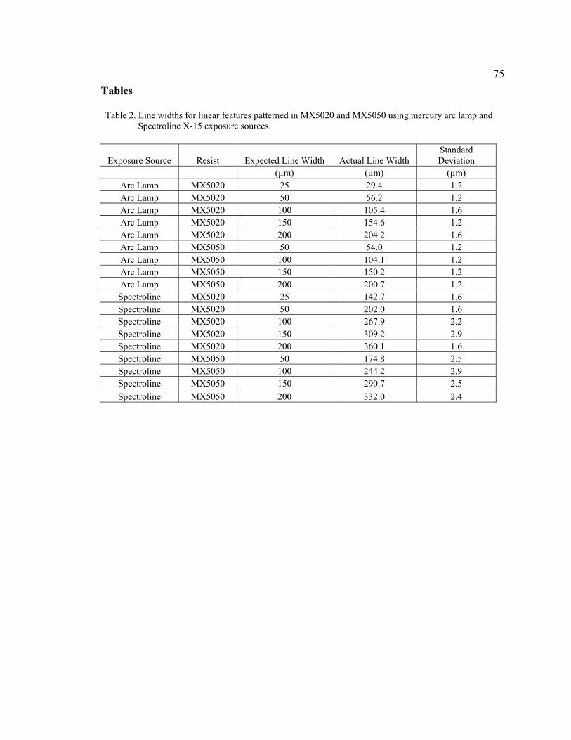
75Tables
Table 2. Line widths for linear features patterned in MX5020 and MX5050 using mercury arc lamp and Spectroline X-15 exposure sources.
Exposure Source Resist Expected Line Width Actual Line Width Standard Deviation
(µm) (µm) (µm) Arc Lamp MX5020 25 29.4 1.2 Arc Lamp MX5020 50 56.2 1.2 Arc Lamp MX5020 100 105.4 1.6 Arc Lamp MX5020 150 154.6 1.2 Arc Lamp MX5020 200 204.2 1.6 Arc Lamp MX5050 50 54.0 1.2 Arc Lamp MX5050 100 104.1 1.2 Arc Lamp MX5050 150 150.2 1.2 Arc Lamp MX5050 200 200.7 1.2 Spectroline MX5020 25 142.7 1.6 Spectroline MX5020 50 202.0 1.6 Spectroline MX5020 100 267.9 2.2 Spectroline MX5020 150 309.2 2.9 Spectroline MX5020 200 360.1 1.6 Spectroline MX5050 50 174.8 2.5 Spectroline MX5050 100 244.2 2.9 Spectroline MX5050 150 290.7 2.5 Spectroline MX5050 200 332.0 2.4

76References [1] C.S. Effenhauser, G.J.M. Bruin, A. Paulus, M. Ehrat, Analytical Chemistry
69 (1997) 3451.
[2] T. McCreedy, Analytica Chimica Acta 427 (2001) 39.
[3] A.P. Sudarsan, V.M. Ugaz, Analytical Chemistry 76 (2004) 3229.
[4] D.C. Duffy, J.C. McDonald, O.J.A. Schueller, G.M. Whitesides, Analytical
Chemistry 70 (1998) 4974.
[5] J.C. McDonald, M.L. Chabinyc, S.J. Metallo, J.R. Anderson, A.D. Stroock,
G.M. Whitesides, Analytical Chemistry 74 (2002) 1537.
[6] D.S. Zhao, B. Roy, M.T. McCormick, W.G. Kuhr, S.A. Brazill, Lab on a
Chip 3 (2003) 93.
[7] A. Pallandre, D. Pal, B. de Lambert, J.-L. Viovy, C. Futterer, Journal of
Physics: Condensed Matter 18 (2006) S665.
[8] M.O. Heuschkel, L. Guerin, B. Buisson, D. Bertrand, P. Renaud, Sensors
and Actuators, B: Chemical B48 (1998) 356.
[9] P. Vulto, N. Glade, L. Altomare, J. Bablet, L.D. Tin, G. Medoro, I.
Chartier, N. Manaresi, M. Tartagni, R. Guerrieri, Lab on a Chip 5 (2005)
158.
[10] Y.-M. Huang, M. Uppalapati, W.O. Hancock, T.N. Jackson, IEEE
Transactions on Advanced Packaging 28 (2005) 564.
[11] Y.-C. Tsai, H.-P. Jen, K.-W. Lin, Y.-Z. Hsieh, Journal of Chromatography,
A 1111 (2006) 267.

77[12] M.E. Sandison, H. Morgan, Journal of Micromechanics and
Microengineering 15 (2005) S139.

78
Chapter 4:
Fabrication of an electroformed ratchet type dielectrophoresis
device
Submitted to Sensors and Actuators B P.O. Box 211 1000 AE Amsterdam, The Netherlands
79
Abstract
Presented is the fabrication of an electroformed ratchet type dielectrophoresis
device. Discussed are the processes used in the fabrication of the required device
components: electrode features patterned onto a glass slide using UV-LIGA and
wet etching, and a PDMS fluidic component produced through replica molding.
Two distinct PDMS components were used to show how the device can be
configured as either a flow-through system or non-flow-though system.
4.1 Introduction
With the advent of micro-electromechanical systems (MEMS) brought forth by
advances in the semiconductor industry and improved machining technology, the
electrokinetic phenomenon of dielectrophoresis (DEP) has made a recent
resurgence due to the possibility of creating devices with smaller interelectrode
distances. Through dimensional reduction, higher effective field strengths are now
possible using only a few volts applied potential, which were not previously
attainable. The phenomenon of DEP occurs when a dipole moment is induced in a
suspended analyte particle within the confines of an asymmetrical electric field [1-
3]. Depending on the degree of polarization of the analyte particle relative to the
polarization of the suspending medium, motion maybe induced. If the
polarizability of an analyte particle is greater than that of the suspending medium,
the particle will be move to the higher field strength region (positive DEP). If the
particle is less polarizable than the suspending medium the particle will aggregate
80
in the low potential area (negative DEP). If both the analyte particle and
suspending medium are polarized to the same extent the particle will experience
no net movement.
In the past few years, DEP has been successfully implemented in the analysis of a
vast array of sample types. Sample types analyzed include: cells [4,5], E. coli [6-
10], viruses [5,6,11-13], blood serum components [4,5,14-19], latex spheres
[11,14,19-25], and fine particles [26]. Many dielectrophoretic devices have been
successfully constructed, as previously mentioned, via commonly used MEMS
fabrication technology, such as direct write electron beam lithography [25],
micromachining [27], laser machining [28], and lift-off technology
[4,8,10,11,14,24,29]. One avenue which has not been explored, to the best of our
knowledge, in constructing electrodes to produce the asymmetrical required for
operating a DEP device is electroforming through LIGA or UV-LIGA.
Electroforming has been successfully implemented in many fields for the
production of various components. One area where electroforming has been
shown as a viable option is in the injection molding industry for fabricating molds
[30,31]. Another field which has seen success in producing electromolded
components is electrodischarge machining for constructing machining electrodes
[32,33]. Multilevel electroplating has also been shown to be feasible in producing
acceleration sensors, and single mechanical components containing a gear, pinion,

81
and axle [34,35]. Presented here is the fabrication of a microfluidic
dielectrophoresis device containing electroformed electrodes, along with methods
by which to configure the device as a flow-through or non-flow-through system,
depending on the geometry of the poly(dimethylsiloxane) (PDMS) fluidic layer
employed.
4.2 Objectives and Device Description
The aim here is to present how electroforming, which has been successfully
implemented in several fields, can be applied to the field of dielectrophoresis to
produce a microfluidic device containing ten independently addressable ratchet
type electrode sets. The device consists of two main components. The first
component is an electrode layer which was constructed by sputtering conductive
seedlayers onto a glass slide, patterning with dry film photoresist, nickel
electroforming using a nickel sulfamate plating solution, resist stripping, and wet
etching of the unused regions of the conductive seedlayers to electrically isolate
the electrodes. The second component needed is a replica molded PDMS fluidic
layer fabricated using conventional soft lithography technology.
The geometry of the electrode features contained on the glass slide is shown on the
photomask used in patterning the film resist, figure 4.1, and a brief description is
as follows. Each electrode contained three main features: a 2.5 mm square solder
pad onto which electrical connections to a function generator are made, a ratchet

82
type electrode feature for dielectrophoretic manipulation of analyte particles, and
an electrical lead connecting the solder pad and electrode features. The electrode
features had widths of 100 µm and were grown to a height of 20 µm.
Interelectrode distances between electrode pairs were 50 µm at the narrowest
portion and 325 µm at the widest region, and the total length from the narrowest to
widest region is 200 µm. The offset between successive electrode pairs was set to
zero.
The fluidic layer was attained through replica molding of PDMS by using masters
fabricated with silicon wafers patterned with dry film photoresist. Figure 4.2
shows the features contained on the photomasks used produce the masters needed
for replica molding of the PDMS fluidic components, which were required to
render the device as either a flow through or non-flow through system. As can be
seen in figure 4.2, both masters contained similar features. Identical features
included on both master types are: solder pads, electrode leads which join the
solder pad and the ratchet type electrodes, and an outline of the outer-most ratchet
type feature. The difference between these masters is that the flow through
geometry contains a fluidic inlet and outlet. Fluidic access into the ratchet type
electrode regions of the device was attained though use of magnets and a molding
fixture containing a galvanized steel base. The magnets served as posts during the
replica molding of PDMS. Magnets were selected for use as posts because
magnetic forces allow for easy configuration and variety of geometries are
83
possible, as magnets are available in a variety of shapes and sizes [36]. For the
flow through configuration, the magnets were placed at the both ends of the
channel features. In producing the PDMS component of the non-flow through
geometry, a magnet was placed over the electrode region to produce a well into
which to place a sample aliquot.
Final device assembly was accomplished by marrying the PDMS layer onto the
electrode feature layer to produce a conformal seal. Conformal sealing was
selected because this method allows for disassembly of the device for cleaning,
thereby making the device reusable. By constructing the PDMS fluidic layer to
contain negative images of the electroformed electrodes, reproducible registration
between the device components can be attained over numerous cleanings.
4.3 Experimental
4.3.1 Reagents and Materials
Borosilicate glass slides, 50 mm by 75 mm, used as substrates onto which the
electrodes were electroformed, were purchased from VWR (West Chester, PA,
USA). The conductive seedlayers required for electroforming were sputtered onto
the glass slides by Sulzer Metaplas Inc. (RI, USA), and the seedlayers deposited
were a 40 nm layer of titanium and a 50 nm layer of copper. Mechanical grade
silicon wafers, 3 inch radius, for use as substrates for masters were purchased from
University Wafers (South Boston, MA, USA). A dry-film photoresist, Dupont

84
MX-5000 series, used for laminating and patterning was purchased from
Microchem (Newton, MA, USA). Photoresist thicknesses of 20 µm (MX-5020)
and 50 µm (MX-5050) were used. AutoCAD 2007 (Autodesk, San Rafael, CA,
USA) software was used for designing of the Mylar transparencies for use as
photomasks during resist exposure. Upon designing, the Mylar transparencies
were then photoplotted by CAD/Art Services, Inc. (Bandon, OR, USA). Acetone
and methanol (Northwest Solvents, Eugene, OR, USA) of technical grade were
used for rinsing substrate surfaces. Spectroscopic grade methanol (Mallinckrodt
Chemicals, Phillipsburg, NJ, USA) was used as a lubricant during alignment of the
PDMS cover layer with the electrode layer. Ultrapure water from a Barnstead E-
Pure system (Dubuque, IA, USA) was used for rinsing and solution preparation.
An aqueous 0.75% resist developing solution was prepared from Dupont D-4000
IC concentrated developer, and was purchased from Microchem. The 300 ppm
calcium carbonate developing rinsing solution was produced from technical grade
calcium carbonate (J.T. Baker, Phillipsburg, PA, USA). Sylgard 184 silicone
elastomer kit (Dow Corning Corp., Midland, MI, USA) was used for production of
the PDMS cover layer. Neodymium magnets used as posts to create fluidic vias
during PDMS replica molding were purchased from K&J Magnetics, Inc.
(Jamison, PA, USA). Nickel Sulfamate RTU mechanical agitation plating solution
and nickel anode were purchased from Technic Inc. (Anaheim, CA, USA).
Dynasolve 2000 (Dynaloy Engineered Chemistries, Indianapolis, IN, USA) was
used for removal of the photoresist after electroforming of the nickel electrodes.

85
Ferric chloride solution (MG Chemicals, Surrey, Canada) was used for etching of
unused portions of the copper seedlayer. Reagent grade hydrogen peroxide
(Mallinckrodt Chemicals, Phillipsburg, NJ, USA) and potassium hydroxide
(Mallinckrodt Chemicals, Phillipsburg, NJ, USA) were used to produce a 1:1
mixture of 5% hydrogen peroxide and 5% potassium hydroxide for use as an
etchant for removal of the titanium seedlayer, exposed upon etching of the copper
seedlayer.
4.3.2 Equipment
A home-made oxygen plasma etching system for descumming substrate surfaces
prior to lamination and electroforming was used. The plasma system was
constructed using a 6 inch x 10 inch 4-port stainless steel vacuum chamber from
MDC Vacuum Products Corporation (Hayward, CA, USA), and an Evactron
Decontaminator RF Plasma Cleaner from XEI Scientific (Redwood City, CA,
USA). For laminating substrates with photoresist, a homemade rolling pin
constructed by inserting a glass rod into a piece of rubber tubing was employed.
For removal of any resist imperfections resulting from the lamination process, a
rubber squeegee was used to smooth the resist. One foot square by quarter inch
thick aluminum plates (McMaster-Carr, Los Angeles, CA, USA) were used to
press the resist onto the substrate surface, thus improving resist adhesion. Resist
exposure was accomplished using a homemade UV flood exposure system
consisting of an Oriel 6186 mercury arc lamp (Oriel Light Sources and
86
Spectroscopy Instrumentation, Stratford, CT, USA) and a Durst 606 photo enlarger
(purchased used, locally) to direct the UV light at a right angle towards the
substrate. For resist development, a Paschee VLS airbrush (Chicago, IL, USA)
was utilized. To attain appropriate registration between the PDMS cover layer and
the electrode layer a Leica Wild Stereozoom microscope (Wetzlar, Germany) was
employed. For imaging, a Zeiss Axiotron (Carl Zeiss MicroImaging, Inc.,
Thornwood, NY, USA) equipped with a Sony Power HAD DXC-970MD camera
(Sony Corporation, New York, NY, USA) and ImagePro Plus 6.0
(MediaCybernetics, Silver Spring, MD, USA) was used. A Dynatronix (Amery,
WI, USA) DuP 10-1-3 pulsed power supply was used to electroform the nickel
electrodes. For determining the plating rate of nickel, a Veeco Dektak 8 Stylus
Profiler fitted with a 12.5 µm tip (Veeco Instruments Inc., Woodbury, NY, USA)
was employed.
4.3.3 Device Fabrication
Electrodes were fabricated using Ti-Cu seedlayer coated glass slides which were
patterned using dry film resist, and then electroformed with nickel to produce the
desired electrode features. The second portion of the device is a replica molded
PDMS slab patterned with necessary fluidic features.

87
4.3.3.1 Photolithography
Both of the above mentioned components were constructed using a
photolithographic approach with a dry film photoresist, described in greater detail
in chapter 3. The resist came supplied in a roll from the manufacturer encased
between a polyethylene layer and polyester layer. For the electrode layer,
lithography was employed for creating void spaces into which nickel was then
electroformed to create the electrode features. The PDMS slab containing the
required fluidic features was cast onto a master containing negative features of the
final desired PDMS component. Due to the commonality in producing the above
mentioned components, the photolithography process engaged will be addressed
separately.
First, the surface of the substrate (either the seedlayer sputtered glass slide or
silicon wafer) to be laminated with resist was rinsed with acetone, methanol,
ultrapure water, and then dried with a stream of nitrogen gas. The surface was
then descummed using an oxygen plasma for 1 min. at a chamber pressure of 200
mTorr and a power of 20 W.
The cleaned surface was then laminated with the dry film photoresist as follows.
The resist was prepared for lamination by removal of the polyethylene layer. Then
by using a homemade rolling pin, the resist was laminated onto the substrate.

88
Imperfections occurring during the lamination process were then removed by first
placing the laminated substrate onto an aluminum plate at 95 °C to soften the
resist. Once the resist had softened, its surface was smoothed using a rubber
squeegee and was pressed between two aluminum plates at 95 °C for 30 s to
improve the adhesion between the resist and surface being laminated. The
laminated substrate was then baked in a 65 °C oven for 20 min., then placed in a
dark drawer and allowed to cool to room temperature.
To produce the negative image of either the final electrode features to be
electroformed or the PDMS fluidic component, a Mylar transparency was
employed. The transparency was placed in contact with the photoresist under a
glass slide. The assembly was then exposed with a UV flood exposure system for
1.5 min or 2 min for electroform masking and PDMS master production,
respectively. The now exposed resist laminated substrate was then baked for 25
min on an 85 °C hot plate.
Developing and rinsing of the photoresist was accomplished using 0.75 vol. % D-
4000 IC concentrated developer solution and an aqueous 300 ppm calcium
carbonate solution, respectively. Prior to use, the developing solution and rinsing
solution were warmed to 45 °C in a water bath. The unexposed photoresist was
developed by first removing the polyester layer from the resist surface, and then
soaking the resist laminated substrate in developing solution for 5 min. The

89
substrate was sprayed with carbonate rinsing solution, and then fully developed
using an airbrush operated at 12 psi of nitrogen gas to apply the developer. After
rinsing a final time with the carbonate rinsing solution, the patterned substrate was
rinsed with ultrapure water, dried under a stream of nitrogen gas, and baked for 25
min on a 100 °C hot plate.
4.3.3.2 Electrode Fabrication
Electrode fabrication was accomplished by electroforming nickel into the voids
created in the resist on the coated glass slide as a result of the lithographic
processing. Following electroforming, the resist was removed from the substrate
surface and then the exposed seedlayers were removed using conventional wet
etching processes. The process utilized is described in detail below.
4.3.3.2.1 Electroforming of Electrodes
Electroforming of nickel electrodes was conducted using a ready made nickel
sulfamate plating solution and a pulsed DC power supply. The plating bath
temperature was 49 °C, pH 4, and was stirred using a magnetic stir bar. The nickel
anode was covered with filter paper to reduce the possibility of introducing anode
residues produced during the electroforming process. Prior to electroforming, the
cathodes (resist-patterned, seedlayer-coated glass slides) were cleaned and
prepared for electroforming by cleaning in an oxygen plasma at 200 mTorr and 22
W for 1 min. to descum the exposed copper surface of any residues remaining

90
from the lithography processing. The copper surfaces of the cathodes were
prepared for electroforming by rinsing with diluted detergent and ultrapure water
to remove any residual organics, then immersing into a 20% H2SO4 solution and
rinsing with ultrapure water to remove any oxides from the copper surface.
Once cleaned, the patterned glass slide was connected to the cathode of the power
supply. The anode and cathode were then submerged in the plating bath. The
power supply pulse duty cycle was set to 1.5 ms on and 0.5 ms off, and the plating
current was set to 40 mA to produce a current density of 2.2 A/dm2. A plating rate
of 0.4 µm/min was established with the above conditions, and thus a total plating
time of 50 min was required to obtain electrodes with a final height of 20 µm.
4.3.3.2.2 Resist Stripping and Seedlayer Removal
Once the electroformed nickel electrodes were produced, the electrodes were made
independently addressable by removing the sputtered conductive seedlayers found
around the nickel features by first stripping the photoresist and then wet etching
the portions of the seedlayers exposed upon removal of the resist. Photoresist
removal was accomplished by immersing the electroformed substrate into a beaker
containing Dynasolve 2000 until the resist was completely stripped. The entire
surface is rinsed with acetone, methanol, and ultrapure water and dried under
nitrogen. The exposed copper seedlayer was then removed by coating the surface
with a thin film of concentrated FeCl3 solution at 55 °C, then rinsing with
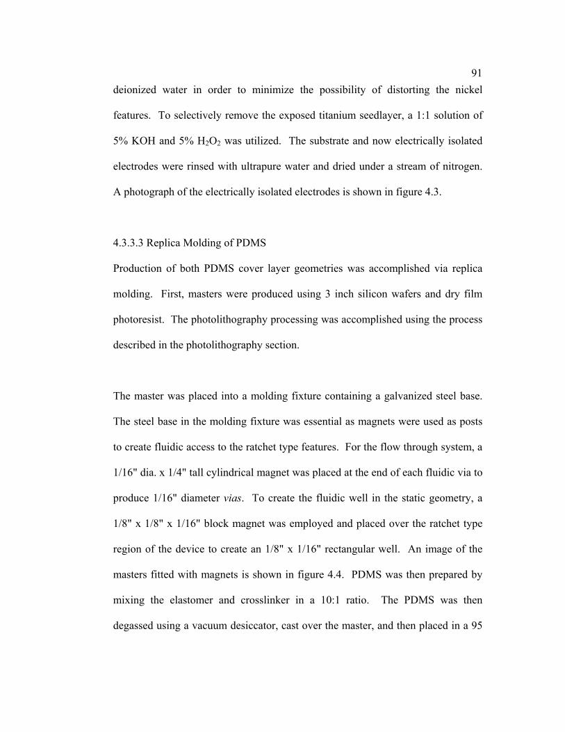
91
deionized water in order to minimize the possibility of distorting the nickel
features. To selectively remove the exposed titanium seedlayer, a 1:1 solution of
5% KOH and 5% H2O2 was utilized. The substrate and now electrically isolated
electrodes were rinsed with ultrapure water and dried under a stream of nitrogen.
A photograph of the electrically isolated electrodes is shown in figure 4.3.
4.3.3.3 Replica Molding of PDMS
Production of both PDMS cover layer geometries was accomplished via replica
molding. First, masters were produced using 3 inch silicon wafers and dry film
photoresist. The photolithography processing was accomplished using the process
described in the photolithography section.
The master was placed into a molding fixture containing a galvanized steel base.
The steel base in the molding fixture was essential as magnets were used as posts
to create fluidic access to the ratchet type features. For the flow through system, a
1/16" dia. x 1/4" tall cylindrical magnet was placed at the end of each fluidic via to
produce 1/16" diameter vias. To create the fluidic well in the static geometry, a
1/8" x 1/8" x 1/16" block magnet was employed and placed over the ratchet type
region of the device to create an 1/8" x 1/16" rectangular well. An image of the
masters fitted with magnets is shown in figure 4.4. PDMS was then prepared by
mixing the elastomer and crosslinker in a 10:1 ratio. The PDMS was then
degassed using a vacuum desiccator, cast over the master, and then placed in a 95
92
°C oven for 1 hr. The magnets used as posts were then removed and the PDMS
was peeled from the master.
4.3.3.4 Device Assembly
Prior to mating the glass slide containing the electrode features with the replica
molded PDMS component, rosin core lead solder was added to the nickel contact
leads located on the glass slide. To prevent flux and solder contamination
elsewhere on the slide, all other electroformed electrode features were covered
with a piece of foil. The replica molded PDMS component was then trimmed to
contain only the features corresponding to the electroformed leads, ratchet types,
and fluidic component features. In the case of the PDMS component configured
with the well geometry, the PDMS meniscus around the well was removed using a
razor blade to yield a flat surface onto which to place a glass microscope cover
slip.
Registration between the patterned PDMS component and glass slide containing
the electroformed features was attained using a process used to align oxygen
plasma activated PDMS surfaces [37]. This process uses an organic solvent (in
this application, methanol) which acts as a lubricant and preserves the activated
PDMS surface. A few drops of methanol were placed on both surfaces to be
mated together. Then the layers were aligned using a microscope. Upon

93
alignment, the assembly was placed in a 95 °C oven to evaporate the methanol.
Figure 4.4 shows the assembled devices.
4.4 Results and Discussion
Proper device function was tested using the non-flow through configuration. To
test if particles will collect in the high potential regions (positive DEP) and low
potential regions (negative DEP) magnetite and polystyrene particles were used,
respectively. The particles were found to collect in appropriate regions over a
frequency range of 60 Hz to 20 MHz, and a representative example is shown in
figure 4.5. During these analyses, the PDMS fluidic component was removed to
clean the electroformed ratchet type features, and was realigned in a reproducible
manner due to the mating between the electrodes and their negative images cast
into the PDMS. In chapter 5 a thorough explanation of the operation of this device
and the above results will be presented, as the aim of this work was to show the
feasibility of constructing a dielectrophoretic device containing electroformed
nickel electrodes.
4.5 Summary and Outlook
A microfluidic ratchet type dielectrophoreis device was constructed using UV-
LIGA, wet etching, and replica molding of PDMS. The device was successfully
constructed with ten electroformed electrode pairs, which can be independently

94
controlled. The electrode assembly was fitted with replica molded PDMS to
configure the device as either a flow-through or static system. Appropriate
registration between the electrode layer and fluidic layer of the device was aided
by the manufacturing techniques selected in fabricating the device, electroforming
and replica molding. With electroformed electrodes and a replica molded PDMS
fluidic component containing a negative image the electrodes, the PDMS fluidic
layer was easily coupled onto the electrode layer.
Electroforming was shown to be a viable method for the production of this
dielectrophoretic device. An area of the electroforming process which will require
further optimization is the lithographic processing in order to produce straighter
electrode sidewalls. As illustrated in figure 4.3, some of the electroformed
electrodes contain regions where the nickel features contain slightly rough
sidewalls. One possible option which may rectify this problem includes use of a
developing station. Use of a developing station will allow for reproducible
photoresist development by having temperature control of the developer,
consistent spray pressure/developer flow, and thus eliminating human error.

95
Figures
Figure 4.1. AutoCAD images of the photomask used to pattern the desired electrode pattern onto the glass substrate.
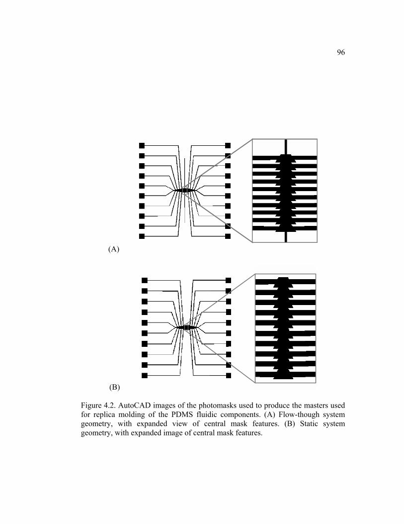
96
(A)
(B)
Figure 4.2. AutoCAD images of the photomasks used to produce the masters used for replica molding of the PDMS fluidic components. (A) Flow-though system geometry, with expanded view of central mask features. (B) Static system geometry, with expanded image of central mask features.

97
Figure 4.3. Photomicrograph of the electrically isolated electroformed nickel electrode features.

98
(A) (B)
(C) (D)
Figure 4.4. Photographs of the masters used for replica molding of the PDMS fluidic layer, and the final mating of the replica molded PDMS component onto the electrode features. (A) Flow-through master. (B) Static system master. (C) Assembled flow through device. (D) Assembled non-flow through device.

99
(A) (B)
Figure 4.5. Images showing particle collection while subjected to an asymmetrical electric field, 2 VRMS at a frequency of 500 kHz. (A) Magnetite collection at the electrode tips under an induced positive dielectrophoretic moment. (B) Polystyrene spheres aggregating under negative dielectrophoresis in the low potential region of the ratchet geometry.

100
References
[1] H.A. Pohl, Journal of Applied Physics 22 (1951) 869.
[2] H.A. Pohl, Cambridge Monographs on Physics. Dielectrophoresis: The
Behavior of Neutral Matter in Nonuniform Electric Fields, 1978.
[3] T.B. Jones, Electromechanics of Particles, Cambridge University Press,
1995.
[4] J. Park, B. Kim, S.K. Choi, S. Hong, S.H. Lee, K.-I. Lee, Lab on a Chip 5
(2005) 1264.
[5] C.M. Das, F. Becker, S. Vernon, J. Noshari, C. Joyce, P.R.C. Gascoyne,
Analytical Chemistry 77 (2005) 2708.
[6] B.H. Lapizco-Encinas, R.V. Davalos, B.A. Simmons, E.B. Cummings, Y.
Fintschenko, Journal of Microbiological Methods 62 (2005) 317.
[7] M. Castellarnau, A. Errachid, C. Madrid, A. Juarez, J. Samitier,
Biophysical Journal 91 (2006) 3937.
[8] S.-H. Oh, S.-H. Lee, S.A. Kenrick, P.S. Daugherty, H.T. Soh, Journal of
Proteome Research 5 (2006) 3433.
[9] J. Suehiro, A. Ohtsubo, T. Hatano, M. Hara, Sensors and Actuators, B:
Chemical B119 (2006) 319.
[10] E.T. Lagally, S.-H. Lee, H.T. Soh, Lab on a Chip 5 (2005) 1053.
[11] I. Ermolina, J. Milner, H. Morgan, Electrophoresis 27 (2006) 3939.
[12] A. Docoslis, L.A. Tercero Espinoza, B. Zhang, L.-L. Cheng, B.A. Israel, P.
Alexandridis, N.L. Abbott, Langmuir 23 (2007) 3840.

101
[13] F. Grom, J. Kentsch, T. Mueller, T. Schnelle, M. Stelzle, Electrophoresis
27 (2006) 1386.
[14] C.-P. Luo, A. Heeren, W. Henschel, D.P. Kern, Microelectronic
Engineering 83 (2006) 1634.
[15] B.P. Lynch, A.M. Hilton, G.J. Simpson, Biophysical Journal 91 (2006)
2678.
[16] Y. Huebner, K.F. Hoettges, G.E.N. Kass, S.L. Ogin, M.P. Hughes, IEE
Proceedings: Nanobiotechnology 152 (2005) 150.
[17] Q. Ramadan, V. Samper, D. Poenar, Z. Liang, C. Yu, T.M. Lim, Sensors
and Actuators, B: Chemical B113 (2006) 944.
[18] M. Borgatti, L. Altomare, M. Baruffa, E. Fabbri, G. Breveglieri, G.
Feriotto, N. Manaresi, G. Medoro, A. Romani, M. Tartagni, R. Gambari, R.
Guerrieri, International Journal of Molecular Medicine 15 (2005) 913.
[19] H. Zhou, L.R. White, R.D. Tilton, Journal of Colloid and Interface Science
285 (2005) 179.
[20] J.D. Yantzi, J.T.W. Yeow, S.S. Abdallah, Biosensors & Bioelectronics 22
(2007) 2539.
[21] D. Chen, H. Du, W. Li, H. Gong, Key Engineering Materials 326-328
(2006) 281.
[22] D. Chen, H. Du, W. Li, H. Gong, Key Engineering Materials 326-328
(2006) 253.

102
[23] D. Holmes, M.E. Sandison, N.G. Green, H. Morgan, IEE Proceedings:
Nanobiotechnology 152 (2005) 129.
[24] D. Holmes, H. Morgan, N.G. Green, Biosensors & Bioelectronics 21
(2006) 1621.
[25] I. Ermolina, H. Morgan, Journal of Colloid and Interface Science 285
(2005) 419.
[26] N. Flores-Rodriguez, G.H. Markx, Journal of Physics D: Applied Physics
39 (2006) 3356.
[27] P. Singh, N. Aubry, Electrophoresis 28 (2007) 644.
[28] R. Pethig, J.P.H. Burt, A. Parton, N. Rizvi, M.S. Talary, J.A. Tame, Journal
of Micromechanics and Microengineering 8 (1998) 57.
[29] T. Yasukawa, M. Suzuki, H. Shiku, T. Matsue, Chemical Sensors 20
(2004) 382.
[30] C.K. Chung, C.J. Lin, C.C. Chen, Y.J. Fang, M.Q. Tsai, Microsystem
Technologies 10 (2004) 462.
[31] M. De Vogelaere, V. Sommer, H. Springborn, U. Michelsen-
Mohammadein, Electrochimica Acta 47 (2001) 109.
[32] F.E.H. Tay, E.A. Haider, The International Journal of Advanced
Manufacturing Technology 18 (2001) 892.
[33] A.E.W. Rennie, C.E. Bocking, G.R. Bennett, Journal of Materials
Processing Tech. 110 (2001) 186.

103
[34] W. Qu, C. Wenzel, G. Gerlach, Sensors and Actuators, A: Physical A77
(1999) 14.
[35] H. Lorenz, L. Paratte, R. Luthier, N.F. de Rooij, P. Renaud, Sensors and
Actuators, A: Physical A53 (1996) 364.
[36] C. Koch, in Personal communication.
[37] B.H. Jo, L.M. Van Lerberghe, K.M. Motsegood, D.J. Beebe,
Microelectromechanical Systems, Journal of 9 (2000) 76.
104
Chapter 5:
Evaluation of a ratchet type dielectrophoretic device
Submitted to Analytical Chemistry 1155 16th St., NW, Washington DC 20036
105
Abstract
Dielectrophoreis is an electrokinetic phenomenon which utilizes an asymmetric
electric field to separate analytes based on their polarizability relative to the
polarizability of the suspending agent. One dielectrophoretic device geometry
which offers interesting possibilities for particle transport without the use of
external flow are ratchet devices. Shown are the initial tests of a novel electrode
based dielectrophoretic ratchet type device geometry using a series of fine test
particles. The asymmetrical electric field required to selectively transport target
analytes has been produced for the first time using electroformed electrodes which
offer the possibility of reducing convective heating and can be used to construct a
device where all particles located within the fluidic channel are exposed to the
applied field. Initial results of the examination of this device were conducted
using fine particle test analytes to show selective particle collection and a
separation based on the electrical properties of the analytes employed.

1065.1 Introduction
The use of electrokinetic phenomena in the field of separations has seen increased
use in the analytical laboratory. Electrokinetic separations offer the analyst the
ability to conduct a separation based on the electronic state of an analyte while
subjected to an electric field gradient. The electronic properties of an analyte
exposed to an electrical field which can be exploited to conduct separations are
charge to mass ratio and relative polarizability of an analyte. Electromechanical
separation techniques used to harness the above mentioned electrical properties are
electrophoresis and dielectrophoresis (DEP), respectively. As stated,
electrophoretic separations are based on differences in the charge to mass ratios of
the analytes being studied, and this makes electrophoresis applicable only to the
separation of charged species. DEP, unlike electrophoresis, is applicable to neutral
species because particles are separated by inducing a dipole moment in an analyte
particle confined within an asymmetrical electric field. Since theses separations
are dependent on the polarizability of a suspended particle, the analyte being
examined can be either neutral or charged.
The first investigations into conducting particle movement and separations of
neutral species through induced dipoles in an asymmetrical field was Herbert Pohl
[1,2]. In these studies, Pohl studied the motion of suspended polymer spheres in
and organic medium, and found that particle migration in an asymmetrical field
was dependent on the polarizability of the suspended polymers relative to the

107polarizability of the suspending medium. He determined that particles more
polarized than the suspending agent will collect in regions of high field intensity
within the applied nonuniform field, positive DEP. For particles less polarized
than the suspending medium, the particles were shown to collect in regions of low
field intensity, negative DEP These studies laid the groundwork for the field of
dielectrophoresis which has been gaining popularity in recent years with the
growing success of microfluidic devices.
Currently, two classes of microfluidic based dielectrophoretic devices have been
successfully employed to create a nonuniform electric field. The first class of DEP
devices in current use is known as insulator based dielectrophoresis [3-16].
Insulator based dielectrophoreis devices function by using insulators placed
between a set of electrodes to produce the required nonuniform electric field. The
second class of devices is electrode DEP devices, which utilize the electrode
geometry to create the required asymmetrical field [17-47].
One device geometry which has been investigated in both electrode and insulator
based devices is a ratchet geometry [16,48-51] The theoretical aspects of ratchet
mechanisms were first presented by Curie [52] and later Feynman [53], and by
adapting these works the theoretical basis of dielectrophoretic ratchets was
developed [54,55]. Ratchet based dielectrophoretic systems have been applied in
the collection of particles under dielectrophoretic forces [16,48-51], and more

108importantly, ratchet configurations offer the possibility of particle movement
through the ratchet device without the use of an external agent (Brownian ratchets
and stacked ratchets) [48-51]. Though ratcheting devices offer the possibility of
particle movement without the need of an external force for electrode based
systems, the relatively large surface areas used create sufficient thermal motion
which counters the dielectrophoretic force exerted on a polarizable particle [51].
Presented is the initial study of a new ratchet type dielectrophoretic device
containing ten independently addressable electroformed electrode pairs. Also
presented is the first use of electroforming technology in the construction of DEP
electrodes. For this study, a series of fine particles of known dielectric properties
were utilized to theoretically determine their collection within an asymmetrical
electric field. Test suspensions containing a single particle type were then
examined to verify appropriate device operation by observing particle collection,
relative to the theoretical expectation, within the asymmetrical electric. A particle
test mixture was also examined to determine the feasibility in conducting a
separation with this device geometry.
5.2 Theory
When a polarizable particle is subjected to an electrical field, a dipole moment will
be induced in the particle regardless of whether it is charged or neutral [2,56]. If
the electric field is asymmetrical a force imbalance will be exerted on the polarize

109particle, which is the basis of dielectrophoretic separations. As a result of the
imbalanced force, a polarized particle will move in accordance with its
polarizability relative to the polarizability of the medium and the angular
frequency of the applied potential [2,56]. A particle more polarized than the
suspending medium will experience positive DEP and will migrate towards a
region of high field intensity. When a particle is less polarized than the
suspending media particle will collect in a region of lower field intensity via a
negative dielectrophoretic moment [2].
The dielectrophoretic force experience by a polarized particle can be determined
by:
( )[ ] 23 Re2 rmsDEP EKrF ∇= ωπ (2)
where r is the radius of a spherical particle, ∇ is the del vector operator, and Erms is
the root mean square applied electric field, and Re[K(ω)] is the real component of
the Clausius-Mossotti factor [56].
The Re[K(ω)] accounts for the in-phase polarization of a suspended particle
relative to the polarization of the suspending media, when using an AC waveform
[32,56,57]. The Re[K(ω)] is determined by taking the real component of the
complex form of the Clausius-Mossotti factor:

110
( ) ( )( )∗∗
∗∗
+
−=
mp
mpKεεεε
ω (3)
where εp∗ and εm
* are the complex dielectric permittivities of the particle and
medium, respectively. The complex dielectric permittivity for a particle or
medium is found by ε*= ε-jσ/ω where ε is the dielectric permittivity, j is √-1, σ is
the conductivity, and ω is the angular frequency of the applied electric field.
A derivation which shows the relation between Re[K(ω)] and the frequency of the
applied field is [58]:
( )[ ] ( )( ) ( )222 12
32
ReMWmpMW
mppm
mp
mpKτωσστ
σεσεεε
εεω
+−
−+
+
−= (4)
where τMW is the Maxwell-Wagner charge relaxation time given by τMW = (εp +
2εm)/(σp + 2σm), and accounts for the relaxation rate of free charges along the
surface of an analyte particle while inducing a dipole moment. Calculations of the
Re[K(ω)] will have values in the range of -0.5 to +1.0 [56]. These values for the
Re[K(ω)] can be used to determine if a particle, of known electrical properties,
will experience positive DEP (values greater than zero) or negative DEP (values
less than zero) for a given suspending medium and frequency. Thus by solving for
the Re[K(ω)] using equation (4), an a priori approach can be taken to determine
the frequency ranges a particle will experience positive or negative DEP.

111
5.3 Experimental
5.3.1 Device Design and Description
The dielectrophoretic devices examined were constructed of two separate
components. The first component was the electroformed nickel electrode features
constructed on conductive seedlayer coated borosilicate glass slides.
Electroforming was employed to fabricate the electrodes for two reasons. First,
electroformed features can be placed within a microfluidic device to create channel
walls composed of electrodes and thus reduce the electrode surface area in contact
with the suspending media, which can reduce the possibility of conductive heating.
Secondly by having a device with electrode walls, all analytes within the electrode
region of the device will be exposed to the asymmetrical electric field thus creating
the possibility of a more effective dielectrophoretic device. The second
component of the device was a replica molded PDMS stamp patterned with
negative images of the electroformed features and fluidic well located over the
ratchet portion of the electrodes.
The geometry of the electroformed nickel electrode features produced on the glass
slide is shown in figure 5.1. As shown in figure 5.1, each electrode component
consisted of three main features: a square solder pad where electrical connections
were made to a waveform generator, a ratchet type electrode feature for
dielectrophoretic manipulation of test particles, and an electrical connector which

112provided continuity between the solder pad and ratchet feature. All electrode
features had final heights of 20µm and were 100 µm wide, except solder pads
which had widths of 2.5 mm. The offset between successive electrode pairs was
zero. During operation, polarized particles located within the ratchet region of the
device collected in regions A and B which correspond to positive DEP and
negative DEP, respectively.
The fluidic component of this device was constructed of PDMS patterned with
negative features of the electroformed features, and the only exception was that the
resist features on the replica molding master encompassed the entirety of the
ratchet feature region. Fluidic access into the ratchet region of the device was
accomplished using a block magnet placed over the ratchet portion of the master to
create a 1/8” by 1/16” rectangular well. The magnet was held in place by using a
molding fixture constructed with a galvanized steel base. The use of magnets to
serve as posts during replica molding was selected due to the ease of configuration
created from magnetic forces and because of the variation of magnet geometries
available which allowed for an array of post geometries [59].
5.3.2 Materials and Equipment
50 mm by 75 mm borosilicate glass microscope slides (VWR, West Chester, PA)
were used as the substrates onto which the device electrodes were electroformed.
40 nm titanium and 50 nm copper conductive seedlayers needed during the

113electroforming process were obtained through sputtering (Sulzer Metaplas Inc.,
Woonsocket, RI). Replica molding master substrates consisted of 3 inch radius
mechanical grade silicon wafers (University Wafers, South Boston, MA).
Technical grade solvents, acetone and methanol (Northwest Solvents, Eugene,
OR), were used for substrate cleaning. Ultrapure water for rinsing and solution
preparation was obtained from a Barnstead E-Pure system (Dubuque, IA).
The oxygen plasma etching system used for descumming substrate surfaces prior
to lamination and electroforming was homemade and was constructed from a 6
inch x 10 inch 4-port stainless steel vacuum chamber from MDC Vacuum
Products Corporation (Hayward, CA) and an Evactron Decontaminator RF Plasma
Cleaner from XEI Scientific (Redwood City, CA).
20 µm and 50 µm thick Dupont MX-5000 series negative tone photoresists were
used in constructing the replica molding masters and electrode features were
purchased from MicroChem Corp. (Newton, MA). Resist lamination was
accomplished using a homemade rolling pin constructed by inserting a glass rod
into a piece of rubber tubing. A rubber squeegee was used to remove any resist
imperfections resulting from the lamination process. Aluminum plates, one foot
square by quarter inch thick (McMaster-Carr, Los Angeles, CA), were used as a
press to improve resist adhesion to the substrate surface. Mylar transparencies
used as masks during resist exposure were designed using AutoCAD 2007

114(Autodesk, San Rafael, CA). The final Mylar transparencies were photoplotted by
CAD/Art Services, Inc. (Bandon, OR). A homemade UV flood exposure system
was constructed using an Oriel 6186 mercury arc lamp (Oriel Light Sources and
Spectroscopy Instrumentation, Stratford, CT) and the UV light was directed
towards the resist laminated substrate using a Durst 606 photo enlarger (locally
purchased used). The Dupont D-4000 IC concentrated developer used to prepare
the 0.75% aqueous resist developing solution was purchased from MicroChem
Corp. Technical grade calcium carbonate (J.T. Baker, Phillipsburg, PA) was used
to prepare an aqueous 300 ppm calcium carbonate developing rinsing solution.
Spray development was accomplished using a Paschee VLS airbrush (Chicago,
IL).
The PDMS fluidic component was produced using a Sylgard 184 silicone
elastomer kit (Dow Corning Corp., Midland, MI). To create the fluidic well, a
1/8" x 1/8" x 1/16" neodymium block magnets (K&J Magnetics, Inc. Jamison, PA)
were used as posts during PDMS replica molding to create a 1/8" x 1/16"
rectangular fluidic well.
For creating the electroformed electrode features, mechanical agitation Nickel
Sulfamate RTU plating solution and nickel anode were purchased from Technic
Inc. (Anaheim, CA). Electrofroming of the nickel electrodes was obtained through
employment of a Dynatronix (Amery, WI) DuP 10-1-3 pulsed power supply. A
115Veeco Dektak 8 Stylus Profiler fitted with a 12.5 µm tip (Veeco Instruments Inc.,
Woodbury, NY) was used to determine the nickel plating rate. Photoresist
removal upon electroforming of the nickel electrodes was accomplished using
Dynasolve 2000 (Dynaloy Engineered Chemistries, Indianapolis, IN). Copper
seedlayer removal was obtained using a ferric chloride solution purchased from
MG Chemicals (Surrey, Canada). A 1:1 mixture of 5% hydrogen peroxide and 5%
potassium hydroxide used to wet etch the titanium seedlayer, and both the
hydrogen peroxide and potassium hydroxide (Mallinckrodt Chemicals,
Phillipsburg, NJ) were reagent grade.
Alignment lubricant used to register the electrode and PDMS components was
spectroscopic grade methanol (Mallinckrodt Chemicals, Phillipsburg, NJ). A
Leica Wild Stereozoom microscope (Wetzlar, Germany) was used to visualize the
registration between the device components. Test particles used to prepare test
suspensions were Fe3O4 (magnetite) with a size of 5 µm or less (CERAC,
Milwaukee, WI), and polystyrene spheres with 5 µm diameters (Bangs
Laboratories, Inc., Fishers, IN). ACS grade KCl (Mallinckrodt Chemicals,
Phillipsburg, NJ) was used to adjust the conductivity of the suspending medium.
Molecular biology grade polysorbate 20 (VWR Internationsl, West Chester, PA)
was used as an additive in the suspending medium to reduce particle aggregation.
A Zeiss Axiotron (Carl Zeiss MicroImaging, Inc., Thornwood, NY) equipped with
a Sony Power HAD DXC-970MD camera (Sony Corporation, New York, NY) and

116ImagePro Plus 6.0 (MediaCybernetics, Silver Spring, MD) was used for imaging
particle collection during the experiments conducted. To energize the device
electrodes, an Agilent 33220A function/arbitrary waveform generator (Santa
Clara, CA) was employed. Verification of the amplitude and frequency of the sine
wave being output by the function generator was accomplished with a DM 502A
digital multimeter and DC504A counter timer produced by Tektronix (Richardson,
TX).
5.3.3 Device Fabrication
As previously described, two key components will need to be constructed for the
examination of this device. The first component fabricated is a glass slide
containing the electroformed nickel electrode features, and the second portion of
the device consisted of a fluidic component produced through replica molding of
PDMS. The fabrication process used in the construction of the electrode and
fluidic components is illustrated in figure 5.2, and described below.
Resist Processing
The electrode patterning and replica molding masters were both produced using
dry film photoresist. Resist thicknesses employed were 20 µm and 50 µm to
fabricate the replica molding masters and to pattern the conductive glass
substrates, respectively.

117The first step conducted in the film resist processing was lamination, which was
carried out after the substrates were cleaned by rinsing with acetone, methanol,
ultrapure water, drying with nitrogen gas, and then descumming with an oxygen
plasma for 1 min at a chamber pressure of 200 mTorr and a power of 20 W.
Lamination was then accomplished by laminating the film resist onto the substrate
using a rolling pin. The resist was warmed on a 95 °C aluminum plate to soften
the resist, and then a rubber squeegee was used to remove imperfections resulting
during lamination. The laminated substrate was then pressed between two
aluminum plates at 95 °C for a total of 30 s. A 20 min post lamination bake was
conducted using a 65 °C oven, and then the laminated substrate was allowed to
cool to room temperature in a dark drawer.
Resist exposure was conducted using Mylar transparencies and a UV flood
exposure system. The masked resist was exposed to a UV flood exposure system
for 1.5 min for the electrode patterning and 2 min for the replica molding master.
A 25 min post exposure bake was then carried out using a shaded 85 °C hot plate.
0.75 vol. % D-4000 IC concentrated developing solution and an aqueous 300 ppm
calcium carbonate solution, both warmed in a water bath to 45 °C, were used to
develop and rinse the patterned resist. Resist development was conducted by
soaking the resist laminated substrates in developing solution for 5 min, rinsing
with carbonate rinsing solution, and then it was fully developed using an airbrush
118operated at 12 psi. The fully developed resist was then rinsed and dried using
carbonate rinsing solution, ultrapure water, dried with nitrogen gas, and post
development baked on a 100 °C hot plate for 25 min.
5.3.3.1 Electrode Fabrication
Electroforming of nickel electrodes was conducted using a mechanical agitation
nickel sulfamate plating solution and the plating bath parameters were pH of 4,
temperature of 49 °C, and it was agitated with a magnetic stir bar. The anode was
covered with filter paper to minimize anode residues created during electroforming
from contaminating the plating solution. Prior to electroforming, resist-patterned,
seedlayer-coated glass slides were cleaned using in an oxygen plasma at 200
mTorr and 20 W for 1 min to descum and remove resist residues from the exposed
copper seedlayers, rinsed with diluted detergent and ultrapure water to remove
residual organics, and dipped into a 20 % H2SO4 solution and ultrapure water
rinsed to render the copper surface free of oxides. The cathode and anode were
connected to their corresponding terminals and the nickel electrode features were
grown at a rate of 0.4 µm/min to a height of 20 µm. The current density employed
was 2.2 A/dm2, and the pulse rate was 1.5 ms on and 0.5 ms off. The electrodes
were then electrically isolated by first removing of the resist using Dynasolve
2000, and then rinsing with acetone, methanol, and ultrapure water. The exposed
seedlayers were wet etched using FeCl3 solution at 55 °C and a 1:1 solution of 5 %
KOH and 5 % H2O2 to remove the copper and titanium seedlayers, respectively.

119
5.3.3.2 PDMS Fluidic Component
The PDMS fluidic component was produced though replica molding using a
master consisting of a resist patterned silicon wafer. The final PDMS stamp
contained negative features of the solder pads and electrical connects between the
solder pads and ratchet portion. A well allowing fluidic access to the ratchet
portion of the device was incorporated into the resulting PDMS slab. To produce
the fluidic well, a magnet serving as a post during casting was used in conjunction
with a molding fixture containing a galvanized steel base. PDMS was then
prepared by mixing the elastomer and crosslinker in a 10:1 ratio, degassing in a
vacuum desiccator, poured over the master, and cured in a 95 °C for 1 hr. The
magnetic post was then removed prior to peeling the PDMS from the master. The
cured PDMS slab was then trimmed to contain only the fluidic well and electrical
connectors between the ratchet features and the solder pads. The PDMS meniscus
around the well was trimmed using a razor blade to create a flat surface onto which
to place a glass cover slide.
5.3.3.3 Device Assembly
To create electrical connections to the waveform generator, rosin core lead solder
was placed onto nickel solder pads after covering all other electroformed features
with a piece of foil to prevent flux and solder contamination during soldering.
The PDMS fluidic component and electrode component were mated using a

120previously described process used to align oxygen plasma activated PDMS
surfaces [60]. The method used an organic solvent as a lubricant which preserved
the oxygen plasma activated PDMS surfaces required to create an irreversible seal
between the PDMS components. In this case methanol was used as a lubricant, as
only a conformal seal is required. The alignment was accomplished by placing a
few drops of methanol onto the surfaces being mated together, and then using a
microscope the components were appropriately registered. The methanol was then
evaporated by placing the assembly in a 95 °C oven. The fluidic well was then
capped using a microscope cover glass to reduce evaporation of the suspending
media. The final device containing the registered electrode and fluidic
components is shown in figure 5.3.
5.3.4 Device Setup and Examination
The final device was connected to a function generator capable of energizing the
electrodes with a sine waveform with an amplitude 7 Vrms and a frequency of 20
MHz, via electrical leads soldered to the nickel solder pads located onto the glass
slide. The amplitude and frequency of the sine wave applied to the device
electrodes was verified using a digital multimeter and counter/timer. Electrode
pairs were divided into groups using an on/on switch to selectively energize
desired ratchet pairs. Optical observations were made using a microscope
equipped with video capture software to image regions of particle collection.

121In selecting the test particles to verify appropriate device function in collecting
particles in the field maxima and minima an a priori approach was taken by
calculating Re[K(ω)], using equation 4, for particles of known dielectric
properties. From these calculations magnetite and polystyrene were selected
because magnetite would experience positive DEP (Re[K(ω)] > 0) and polystyrene
would undergo negative DEP (Re[K(ω)] < 0). A visual representation of
Re[K(ω)] as a function of frequency for magnetite and polystyrene in 110 µS/cm
water is shown in figure 5.4. The dielectric properties of the particles and medium
used in generating figure 5.4 are listed in Table 3 [61,62].
Using magnetite particles and polystyrene spheres, three separate test particle
solutions were prepared with an aqueous suspending medium consisting of
ultrapure water, 1% polysorbate-20, and a final KCl adjusted conductivity of 110
µS/cm. Appropriate particle collection was conducted using test suspensions
containing only one particle type, and the concentrations for each of these
suspensions were 0.02 w/v % magnetite and 0.0076 w/v % polystyrene latex
spheres. The third suspension consisted of 0.02 w/v % magnetite and 0.0076 w/v
% polystyrene latex spheres, to test the feasibility of separating a sample mixture.
Prior to use, samples were sonicated for 5 min to break up particle aggregates and
vortex mixed to create a uniform suspension. 5 µL sample aliquots were pipetted
into the fluidic well and capped with a glass microscope cover glass.

122To verify the expected results from calculating Re[K(ω)] as shown in figure 5.4,
the single particle test suspensions were studied by energizing the electrodes using
a sine waveform with an amplitude of 2 Vrms. The samples were studied over a
frequency range of 1 kHz to 20 MHz to verify that the magnetite particles and
polystyrene spheres underwent positive DEP and negative DEP, respectively.
Frequencies below 1 kHz were not studied because water electrolysis was a
common occurrence. Once it was established that the particles collected in the
desired regions, the test mixture was studied using a sine waveform with an
amplitude of 2 Vrms and a frequency of 500 kHz
5.4 Results and Discussions
From the plot of Re[K(ω)] as a function of frequency, figure 5.4, it was expected
that the magnetite particles would experience positive DEP and the polystyrene
spheres would undergo negative DEP. To verify that this device would collect the
test particles in the appropriate regions, the single particle test suspensions were
examined using AC waveforms with amplitudes of 2 Vrms and frequencies in the
range of 1 kHz to 20 MHz. From these examinations, it was found that the
magnetite particles underwent positive DEP over the entire frequency range, and
the polystyrene spheres experience negative DEP over the frequency range
studied. Figure 5.5 shows a representative image of the magnetite particles
collecting in pearl chains under positive DEP along the field maxima regions and
the polystyrene spheres aggregating under negative DEP at the field minima
123regions for an applied AC waveform 2 Vrms and 500 kHz. These findings verify
two items. First, the a priori approach in selecting test analytes was valid for the
particles selected. Secondly, this ratchet type dielectrophoretic device is capable
of collecting polarizable particles based on the dielectric properties of the test
analytes employed.
Once it was established that the particles collected in the expected regions of the
asymmetrical electric field, the test mixture containing both magnetite particles
and polystyrene spheres was studied to test for the feasibility of conducting a
separation using this device. For this portion of the experiment, the test mixture
was studied by energizing the ratchet electrodes using a sine waveform with an
amplitude of 2 Vrms and frequency of 500 kHz. As with the single particle test
suspensions, particles were found to collect in the desired regions. Magnetite
particles collected in the high field regions under positive DEP and polystyrene
spheres aggregated in the low field regions through negative DEP. Figure 5.5D is
an image showing a separation of the magnetite/polystyrene mixture. This result
shows that it is possible to selectively collect particles from a mixture into
individual components, and as with the single particle test mixtures, these findings
are also consistent with the theoretical expectations determined by calculating
Re[K(ω)].

124For experiments conducted using magnetite particles two observations were
noticed, which were not encountered for studies conducted with polystyrene
spheres. First, it was found that these particles collected at the high field regions
of unenergized electrode sets. Secondly, the magnetite particles collected on the
surface of the glass substrate in the lower field regions of the ratchet geometry.
The collection of particles along the unenergized electrodes is believed to be
caused by the high conductivity of magnetite, 1000 S/cm, which provided
electrical continuity between the energized and unenergized electrodes. To verify
if the magnetite particles were providing continuity, a digital multimeter and
timer/counter were used to determine if the energized and unenergized electrode
pairs were being energized while applying an AC waveform to selected electrodes.
It was found from the digital multimeter and timer/counter measurements that all
electrode pairs were energized alike. The same procedure was conducted for the
clean polystyrene suspension, and it was determined that the unenergized
electrodes remained unenergized. These findings lead us to believe that the
magnetite particles are responsible for all electrode pairs being energized.
The magnetite particle collection along the surface of the glass substrate is most
likely due to settling effects, figures 5.5.B and 5.5.D. At this time, the settling
effect is believed to be caused by the specific density of the magnetite particles,
5.18 g/cm3 (obtained from the product MSDS), which may result in gravitational

125and frictional forces that counter the dielectrophoretic force. To counter the
problems encountered using magnetite particles a surrogate test particle will need
to be found, which is less conductive and has a lower specific gravity than
magnetite. One possibility are surface modified submicrometer latex spheres,
which have been shown to collect under positive or negative DEP depending on
the particle type, suspending medium, and applied field [19,20,28].
5.5 Conclusions
Presented in this work was the initial evaluation of a new ratchet type
dielectrophoretic device for conducting separations based on the dielectric
properties of suspended particles. Electroforming was selected to manufacture the
device electrodes because electroforming provides the opportunity to impart a
dielectrophoretic force to all analytes located within a fluidic device by allowing
for the construction of devices with electrodes comprising channel walls. In
manufacturing the electrodes for this device, we have successfully shown for the
first time that electroforming is a possible method for producing the electrodes
needed to produce the asymmetrical electric field in a DEP device. This ratchet
device was successfully tested by collecting and separating a series of magnetite
and polystyrene test particle suspensions, which collected in the asymmetrical field
regions dictated by the real component of the Clausius-Mossotti, equation 4.
Future studies include modeling of the asymmetric field, investigations into

126conducting ratcheting mechanisms, and implementation of a dielectrophoretic
device with channel sidewalls comprised of electroformed electrodes.

127
Figures
A
B
C
Figure 5.1. Illustration showing the entire the electrode array and an expanded view of the ratchet region. Electrode features contained include a square solder pad, ratchet type electrode features, and an electrical lead connecting the solder pad and ratchet feature. Dimensions for regions A, B, and C are 50 µm, 325 µm, and 200 µm.
128
Figure 5.2. Schematic outline of the fabrication process used to construct the dielectrophoretic device. (A) Electrode array fabrication: (1) titanium and copper seedlayers sputtering, (2) resist patterning, (3) electroforming of nickel electrodes and resist removal, and (4) removal of exposed seedlayers via wet etching. (B) Fluidic layer fabrication: (1) master constructed using dry film resist and a silicon wafer, and (2) replica molded PDMS containing negative features of the patterned film resist. (C) Mated electrode array and PDMS fluidic component.
(1) Ti then Cu Sputtered Glass slide
(2) Dry film resist for electrode patterns
(3) Electroforming/Resist removal
(4) Ni electrodes on glass (Cu, Ti stripped)
(1) Master fabrication
(2) PDMS replica for fluidic layer
(C) Assembled Microchip with PDMS Fluidic Layer and electrode array
(A) Electrode Array Fabrication (B) Fluidic Layer Fabrication

129
Figure 5.3. Photograph of assembled device consisting of an electrode array, fluidic layer, and microscope cover glass.

130 Figure 5.4. Real component of the Clausius-Mossotti factor (Re[K(ω)]) over the frequency range studied for magnetite and polystyrene.
-0.6
-0.4
-0.2
0
0.2
0.4
0.6
0.8
1
1.2
1.00E+01 1.00E+02 1.00E+03 1.00E+04 1.00E+05 1.00E+06 1.00E+07 1.00E+08
Frequency (Hz)
Re[
K(w
)] PolystyreneMagnetite

131
(A) (B)
(C) (D) Figure 5.5. Images for experiments conducted using magnetite particles and polystyrene spheres at 2 Vrms and 500 kHz. (A) Magnetite particles collecting at the regions of high field intensity under positive DEP. (B) Polystyrene spheres aggregating under negative DEP in regions of low field intensity. (C) Separation of a magnetite/polystyrene mixture.

132Tables
Table 3. Dielectric Properties of Test Particles and Media
Magnetite Polystyrene Water Dielectric Constant 14.2 2.5 78.5 Conductivity (S/cm) 104 10-18 1.1 x 10⁻⁴

133References
[1] H.A. Pohl, Journal of Applied Physics 22 (1951) 869.
[2] H.A. Pohl, Cambridge Monographs on Physics. Dielectrophoresis: The
Behavior of Neutral Matter in Nonuniform Electric Fields, 1978.
[3] E.B. Cummings, A.K. Singh, Proceedings of SPIE-The International
Society for Optical Engineering 4177 (2000) 164.
[4] C.-F. Chou, F. Zenhausern, IEEE Eng Med Biol Mag FIELD Full Journal
Title:IEEE engineering in medicine and biology magazine: the quarterly
magazine of the Engineering in Medicine & Biology Society 22 (2003) 62.
[5] C.-F. Chou, J.O. Tegenfeldt, O. Bakajin, S.S. Chan, E.C. Cox, N. Darnton,
T. Duke, R.H. Austin, Biophysical Journal 83 (2002) 2170.
[6] E.B. Cummings, A.K. Singh, Analytical Chemistry 75 (2003) 4724.
[7] B.H. Lapizco-Encinas, B.A. Simmons, E.B. Cummings, Y. Fintschenko,
Analytical Chemistry 76 (2004) 1571.
[8] B.H. Lapizco-Encinas, R.V. Davalos, B.A. Simmons, E.B. Cummings, Y.
Fintschenko, Journal of Microbiological Methods 62 (2005) 317.
[9] G.J. McGraw, R.V. Davalos, E.B. Cummings, Y. Fintschenko, G.J.
Fiechtner, B.A. Simmons, Polymer Preprints (American Chemical Society,
Division of Polymer Chemistry) 46 (2005) 1208.
[10] L.M. Barrett, A.J. Skulan, A.K. Singh, E.B. Cummings, G.J. Fiechtner,
Analytical Chemistry 77 (2005) 6798.
[11] P. Mela, A. van den Berg, Y. Fintschenko, E.B. Cummings, B.A.
Simmons, B.J. Kirby, Electrophoresis 26 (2005) 1792.
[12] B. Simmons, B. Lapizco-Encinas, R. Shediac, J. Hachman, J. Chames, J.
Brazzle, J. Ceremuga, G. Fiechtner, E. Cummings, Y. Fintschenko, Special
Publication - Royal Society of Chemistry 297 (2004) 171.
[13] B.H. Lapizco-Encinas, B.A. Simmons, E.B. Cummings, Y. Fintschenko,
Electrophoresis 25 (2004) 1695.

134[14] B.A. Simmons, B.H. Lapizco-Encinas, R. Shediac, J. Hachman, J. Chantes,
G. Fiechtner, E. Cummings, Y. Fintschenko, Polymer Preprints (American
Chemical Society, Division of Polymer Chemistry) 45 (2004) 527.
[15] J.O. Tegenfeldt, C. Prinz, H. Cao, R.L. Huang, R.H. Austin, S.Y. Chou,
E.C. Cox, J.C. Sturm, Analytical and Bioanalytical Chemistry 378 (2004)
1678.
[16] C. Marquet, A. Buguin, L. Talini, P. Silberzan, Physical Review Letters 88
(2002) 168301/1.
[17] Y. Huang, R. Pethig, Measurement Science and Technology 2 (1991) 1142.
[18] R. Pethig, Y. Huang, X.B. Wang, J.P.H. Burt, Journal of Physics D:
Applied Physics 25 (1992) 881.
[19] N.G. Green, H. Morgan, Journal of Physics D: Applied Physics 30 (1997)
L41.
[20] H. Morgan, M.P. Hughes, N.G. Green, Biophysical Journal 77 (1999) 516.
[21] Y. Huang, S. Joo, M. Duhon, M. Heller, B. Wallace, X. Xu, Analytical
Chemistry 74 (2002) 3362.
[22] N.G. Green, H. Morgan, Journal of Physics D: Applied Physics 30 (1997)
2626.
[23] N.G. Green, H. Morgan, J.J. Milner, Journal of Biochemical and
Biophysical Methods 35 (1997) 89.
[24] N.G. Green, A. Ramos, H. Morgan, Journal of Physics D: Applied Physics
33 (2000) 632.
[25] S. Tsukahara, T. Sakamoto, H. Watarai, Langmuir 16 (2000) 3866.
[26] S. Tsukahara, H. Watarai, IEE Proceedings: Nanobiotechnology 150
(2003) 59.
[27] K. Ratanachoo, P.R.C. Gascoyne, M. Ruchirawat, Biochimica et
Biophysica Acta, Biomembranes 1564 (2002) 449.
[28] H. Watarai, T. Sakamoto, S. Tsukahara, Langmuir 13 (1997) 2417.
135[29] M.P. Hughes, H. Morgan, F.J. Rixon, J.P.H. Burt, R. Pethig, Biochimica et
Biophysica Acta, General Subjects 1425 (1998) 119.
[30] M.P. Hughes, H. Morgan, Journal of Physics D: Applied Physics 31 (1998)
2205.
[31] Y. Huang, X.B. Wang, J.A. Tame, R. Pethig, Journal of Physics D:
Applied Physics 26 (1993) 1528.
[32] P.R.C. Gascoyne, J. Vykoukal, Electrophoresis 23 (2002) 1973.
[33] P. Gascoyne, C. Mahidol, M. Ruchirawat, J. Satayavivad, P. Watcharasit,
F.F. Becker, Lab on a Chip 2 (2002) 70.
[34] T. Muller, A. Pfennig, P. Klein, G. Gradl, M. Jager, T. Schnelle, IEEE Eng
Med Biol Mag FIELD Full Journal Title:IEEE engineering in medicine and
biology magazine: the quarterly magazine of the Engineering in Medicine
& Biology Society 22 (2003) 51.
[35] T. Muller, G. Gradl, S. Howitz, S. Shirley, T. Schnelle, G. Fuhr,
Biosensors & Bioelectronics 14 (1999) 247.
[36] J. Cheng, E.L. Sheldon, L. Wu, A. Uribe, L.O. Gerrue, J. Carrino, M.J.
Heller, J.P. O'Connell, Nature Biotechnology 16 (1998) 541.
[37] J. Cheng, E.L. Sheldon, L. Wu, M.J. Heller, J.P. O'Connell, Analytical
Chemistry 70 (1998) 2321.
[38] Y. Huang, K.L. Ewalt, M. Tirado, R. Haigis, A. Forster, D. Ackley, M.J.
Heller, J.P. O'Connell, M. Krihak, Analytical Chemistry 73 (2001) 1549.
[39] R. Casanella, J. Samitier, A. Errachid, C. Madrid, S. Paytubi, A. Juarez,
IEE Proc Nanobiotechnol FIELD Full Journal Title:IEE proceedings.
Nanobiotechnology 150 (2003) 70.
[40] X.B. Wang, Y. Huang, X. Wang, F.F. Becker, P.R. Gascoyne, Biophys J
FIELD Full Journal Title:Biophysical journal 72 (1997) 1887.
[41] P.R.C. Gascoyne, J.V. Vykoukal, J.A. Schwartz, T.J. Anderson, D.M.
Vykoukal, K.W. Current, C. McConaghy, F.F. Becker, C. Andrews, Lab
on a Chip 4 (2004) 299.
136[42] C.M. Das, F. Becker, S. Vernon, J. Noshari, C. Joyce, P.R.C. Gascoyne,
Analytical Chemistry 77 (2005) 2708.
[43] B. Prasad, S. Du, W. Badawy, K.V.I.S. Kaler, Measurement Science and
Technology 16 (2005) 909.
[44] E.G. Cen, C. Dalton, Y. Li, S. Adamia, L.M. Pilarski, K.V.I.S. Kaler,
Journal of Microbiological Methods 58 (2004) 387.
[45] A. Ramos, P. Garcia, A. Gonzalez, A. Castellanos, H. Morgan, N.G.
Green, Proceedings of SPIE-The International Society for Optical
Engineering 5839 (2005) 305.
[46] J. Bakewell David, H. Morgan, IEEE Trans Nanobioscience FIELD Full
Journal Title:IEEE transactions on nanobioscience 5 (2006) 139.
[47] A. Docoslis, P. Alexandridis, Electrophoresis 23 (2002) 2174.
[48] J. Rousselet, L. Salome, A. Ajdari, J. Prostt, Nature 370 (1994) 446.
[49] L.P. Faucheux, A. Libchaber, J. Chem. Soc. Faraday Trans 91 (1995) 3163.
[50] L. Gorre-Talini, S. Jeanjean, P. Silberzan, Physical Review E: Statistical
Physics, Plasmas, Fluids, and Related Interdisciplinary Topics 56 (1997)
2025.
[51] L. Gorre-Talini, J.P. Spatz, P. Silberzan, Chaos 8 (1998) 650.
[52] P. Curie, French) Journal de Physique, 3, III, 393-415 (1894).
[53] R.P. Feynman, R.B. Leighton, M. Sands, The Feynman lectures on
physics, Addison-Wesley Redwood City, Calif, 1963.
[54] A. Ajdari, J. Prost, CR Acad. Sci. Paris II 315 (1992) 1635.
[55] J.F. Chauwin, A. Ajdari, J. Prost, Europhysics letters(Print) 27 (1994) 421.
[56] T.B. Jones, Electromechanics of Particles, Cambridge University Press,
1995.
[57] M.P. Hughes, Electrophoresis 23 (2002) 2569.
[58] L. Benguigui, I.J. Lin, Journal of Applied Physics 53 (1982) 1141.
[59] C. Koch, in Personal communication.

137[60] B.H. Jo, L.M. Van Lerberghe, K.M. Motsegood, D.J. Beebe,
Microelectromechanical Systems, Journal of 9 (2000) 76.
[61] D.R. Lide, CRC Handbook of chemistry and physics: a ready-reference
book of chemical and physical data, 83rd ed., by David R. Lide. Boca
Raton: CRC Press, ISBN 0849304830, 2002 (2002).
[62] S. Budavari, M.J. O'Neil, P.E. Heckelman, The merck index an
encyclopedia of chemical, drugs, and biologicals, 1996.

138
Chapter 6: Conclusions

139Two goals comprised the research efforts of this dissertation. The first goal was to
develop the fabrication methodologies necessary in constructing microfluidic
devices. The second aim was to develop a novel microfluidic dielectrophoretic
device to conduct separations of neutral materials.
As detailed in the introduction, several microfluidic based dielectrophoretic
devices exist. Each of these designs operates through the use of an asymmetrical
electric field to collect particles under positive DEP or negative DEP depending on
the polarizability of the analyte relative to the polarizability of the media. The
asymmetrical fields used in these devices can be created through the use of
electrodes of insulators. Commonly used chip based DEP device geometries are
parabolic electrodes, castellated electrode, electrode arrays, and insulator based
geometries. A device geometry which has seen limited use in the field of DEP is
ratchet based systems because of thermal effects which counter the
dielectrophoretic force.
As stated in chapter 2, ratchet systems allow for the collection of particles under
+DEP and –DEP, and at the same time create interesting possibilities for particle
movement without the use of an external flow. We felt the particle collection and
transport possibilities available with a ratchet design warranted an investigation
into designing a novel ratchet type device. In developing the device, we decided a
possible way to optimize the ratchet electrode geometry was to make each ratchet

140portion a separate set of electrodes. This alteration creates the possibility of
energizing each set of electrodes independently. We also felt that electroforming,
a method never previously used in the fabrication of DEP electrodes, would offer
the possibility to create a device with electrodes spanning the entire height of the
fluidic device. We felt if these electroformed electrodes were to be embedded into
a microfluidic device a more thorough dielectrophoretic investigation of a sample
located within a fluidic channel could result. This is because all analytes will be
exposed to the asymmetrical field and a dielectrophoretic force will be experienced
by all polarizable compounds.
Initial attempts in creating the electroformed electrodes for this ratchet type device
were conducted using SU-8 photoresist to pattern a conductive seedlayer coated
glass slides prior to electroforming the nickel features. We selected SU-8 because
of our experience in using this product to create masters for molding soft polymer
devices. SU-8 ultimately was found not to be a viable option for the following
reasons. First, adhesion issues between the copper seedlayer and the SU-8 were a
recurring issue even with the use of adhesion promoters. These adhesion issues
allowed the nickel to plate under the resist resulting in continuity between
successive electrode sets. Secondly, the SU-8 processing method changed on a
daily basis due to the temperature and humidity instabilities of our fabrication
facilities.

141Due to the problems experienced using SU-8, we decided to investigate the use of
a film resist in creating our feature patterning. The film resist selected was a
DuPont MX-5000. This product was selected because it was a negative tone resist
which allowed us to use the same photomasks employed during our attempts in
patterning with SU-8. Also, this product uses aqueous developing and rinsing
solutions, versus the organic developer and rinsing solvent used for SU-8, which
eliminates the creation of organic waste. The film resist was found to a viable
alternative to SU-8 because of the improved adhesion between the resist and the
substrate surface.
The electroforming process was conducted using a mechanically agitated nickel
sulfamate plating solution, and not the air agitated formulation because of the
pitting observed on the electrode surfaces via the agitation method. The
electroformed features were electrically isolated by removal of the resist using an
epoxy stripper, Dynasolve 2000. The un-plated regions of the conductive
seedlayers were then removed using wet etching technology to successfully
fabricate the electroformed electrodes. The etching solutions found not to greatly
impact the electroformed nickel features were FeCl3 and a 1:1 mixture of 5 %
KOH and 5 % H2O2, for removal of the copper and titanium seedlayers
respectively.
142The device was examined for appropriate operation using magnetite particles and
polystyrene latex spheres. These particles were selected as the magnetite is
expected to experience +DEP and polystyrene should undergo –DEP, as expected
from the real component of the Clausius-Mossotti calculations. Test suspensions
of these particles were examined and the test particles were found to collect in the
desired region of the asymmetrical field produced by this ratchet configuration.
The magnetite particles collected at the regions of highest field strength under
+DEP, and the polystyrene spheres experienced –DEP and aggregated in the low
field regions. These findings were found to be consistent with the calculated
results of the real component of the Clausius-Mossotti factor, which leads us to
believe that the device is operating as expected. A test mixture containing
magnetite and polystyrene was also examined to determine the feasibility of
conducting a DEP separation using this device. For this simple two component
mixture the device was capable of separating the mixture into individual
components.
The final electroformed device was shown to operate as expected in collecting
particles under +DEP and –DEP. This novel ratchet device was fabricated using
manufacturing capabilities which were brought to our research group as a result of
this research effort. We also demonstrated, for the first time in the field of DEP,
the use of electroformed electrodes to create the asymmetrical electric field
required for dielectrophoretic manipulation of neutral particles.

143
Using this device, it was shown it is possible to selectively collect neutral particles
based on the dielectric properties of the test analytes employed. Future studies to
be conducted will be to investigate if it will be possible to operate this DEP ratchet
type design in a stacked ratchet mode, as described in chapter 2. To accomplish
this task, the electrode spacing between successive electrode sets will need to be
determined such that the electric field of adjacent electrode sets overlap. This
electric field overlap will ensure a dielectrophoretic force will be exerted on the
collected particles and should allow for movement (ratcheting) of particles. To
determine the required electrode distances, computer modeling will need to be
employed to visualize the electric field.
Though much work will need to be conducted in order to obtain a ratchet device
which moves particles though a fluidic device without the use of external flow, we
feel that this geometry will have positive effects in the field of electokinetics,
microfluidics, and µ-TAS. By providing a means to selectively transport analytes
through a device based on their dielectric properties the cost and use of external
flow sources, such as pumps, will be eliminated.