downloads.semi.orgdownloads.semi.org/web/wstdsbal.nsf/0/e0cfa6df34e86af... · web viewappendix 3...
TRANSCRIPT

Background Statement for SEMI Draft Document 4760NEW STANDARD: MECHANICAL SPECIFICATION FOR FRONT-OPENING SHIPPING BOX USED TO TRANSPORT AND SHIP 450mm WAFERS – Design A and Design BNote: This background statement is not part of the balloted item. It is provided solely to assist the recipient in reaching an informed decision based on the rationale of the activity that preceded the creation of this document.
Note: Recipients of this document are invited to submit, with their comments, notification of any relevant patented technology or copyrighted items of which they are aware and to provide supporting documentation. In this context, “patented technology” is defined as technology for which a patent has issued or has been applied for. In the latter case, only publicly available information on the contents of the patent application is to be provided.
Background
For standardization of FOSB, TF pursued the following requirementsi. Interoperability with 450 FOUP, as far as shipping performance requirements allowii. Shipping performance to protect against accidental package drop during transportation .iii. Storage capability for sufficient periodiv. Transportation efficiency
In the TF activities, the following three designs were proposed and discussed Design A is assuming 2 degree draft angle for achieving the same outer dimensions and same wafer pitch as 450
FOUP. Design B is assuming 3 degree draft angle, and wafer pitch is ~11.1 mm for keeping same height as 450 FOUP. Design C is assuming 3 degree draft angle and have 12 mm wafer pitch for securing random access.
As a consensus of International 450 mm Shipping Box TF, It will be difficult to focus on one design withoutsufficient data, therefore design A and design B were proposed and agreed upon for prototyping and data gathering for the yellow ballot preparation.
The dimensions of some items have not reached consensus in the International 450 mm Shipping Box TF, therefore this blue ballot includes two design proposals for raw Si wafer shipping;
Design A
• Random access (12mm pitch)
• Perimeter support
• Same envelope as FOUP
• Assumptions:
– 2 degree draft angle
– Drop height assumption:
• 200mm palletized shipment
• 510mm individual box shipment
Design B
• Sequential access (reduced pitch ~11.1mm – need confirm)
i
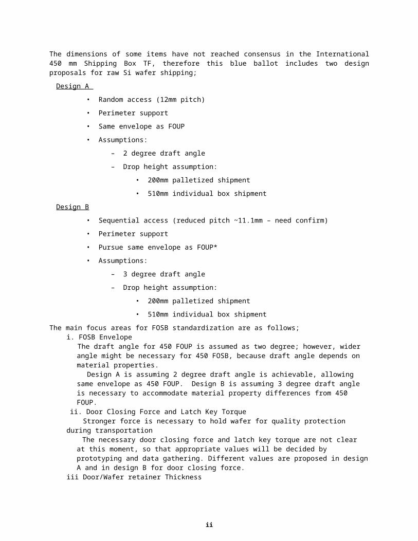
• Perimeter support
• Pursue same envelope as FOUP*
• Assumptions:
– 3 degree draft angle
– Drop height assumption:
• 200mm palletized shipment
• 510mm individual box shipment
The main focus areas for FOSB standardization are as follows;i. FOSB Envelope The draft angle for 450 FOUP is assumed as two degree; however, wider angle might be necessary for 450
FOSB, because draft angle depends on material properties. Design A is assuming 2 degree draft angle is achievable, allowing same envelope as 450 FOUP. Design B
is assuming 3 degree draft angle is necessary to accommodate material property differences from 450 FOUP.
ii. Door Closing Force and Latch Key Torque Stronger force is necessary to hold wafer for quality protection during transportation The necessary door closing force and latch key torque are not clear at this moment, so that appropriate
values will be decided by prototyping and data gathering. Different values are proposed in design A and in design B for door closing force.
iii Door/Wafer retainer Thickness
The wafer warp of 450 mm is larger than 300mm, so that wafer retaining area shall be reviewed for shipping box usage, and for keeping wafer safe during transportation from silicon suppliers to their customers. Different dimensions are proposed for design A and for design B for finding appropriate dimensions by prototyping and data gathering.
The following documents are written by different formats, though the document is to be brushed up for yellow ballot in future. Design A is written by following Doc. 4570B and design B is written by following SEMI M31 (300mm FOSB). The description for Design A is written from page 1 to page 55, and that for Design B is from page 56 to page 84.
This document is also prepared for receiving inputs from interested parties. The results of this informational (Blue) ballot will be discussed early September in regional TFs and in international 450 mm shipping box TF (Web/ TEL conference) on September 17 NA time / 18 JA Time.
ii

INFO
RM
ATIO
NA
L B
ALL
OT
Informational (Blue) Ballot1000AInformational (Blue) Ballotjn l
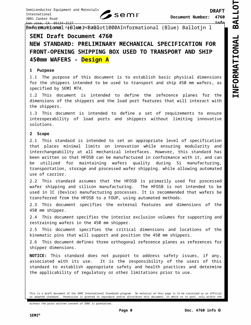
SEMI Draft Document 4760NEW STANDARD: PRELIMINARY MECHANICAL SPECIFICATION FOR FRONT-OPENING SHIPPING BOX USED TO TRANSPORT AND SHIP 450mm WAFERS - Design A1 Purpose1.1 The purpose of this document is to establish basic physical dimensions for the shippers intended to be used to transport and ship 450 mm wafers, as specified by SEMI M74.1.2 This document is intended to define the reference planes for the dimensions of the shippers and the load port features that will interact with the shippers.1.3 This document is intended to define a set of requirements to ensure interoperability of load ports and shippers without limiting innovative solutions.
2 Scope 2.1 This standard is intended to set an appropriate level of specification that places minimal limits on innovation while ensuring modularity and interchangeability at all mechanical interfaces. However, this standard has been written so that HFOSB can be manufactured in conformance with it, and can be utilized for maintaining wafers quality during Si manufacturing, transportation, storage and processed wafer shipping. while allowing automated use of carrier. 2.2 This standard assumes that the HFOSB is primarily used for processed wafer shipping and silicon manufacturing. The HFOSB is not intended to be used in IC (Device) manufacturing processes. It is recommended that wafers be transferred from the HFOSB to a FOUP, using automated methods. 2.3 This document specifies the external features and dimensions of the 450 mm shipper.2.4 This document specifies the interior exclusion volumes for supporting and restraining wafers in the 450 mm shipper.2.5 This document specifies the critical dimensions and locations of the kinematic pins that will support and position the 450 mm shippers.2.6 This document defines three orthogonal reference planes as references for shipper dimensions.
NOTICE: This standard does not purport to address safety issues, if any, associated with its use. It is the responsibility of the users of this standard to establish appropriate safety and health practices and determine the applicability of regulatory or other limitations prior to use.
3 Limitations3.1 The detailed methods and mechanisms inside a 450 HFOSB door as to how a carrier door may be engaged to and disengaged from the carrier shell are not specified by this document.3.2 Since it has not yet been demonstrated that a direct scale-up of the 300 mm shipper and load port methods (i.e., FIMS, how a load port opens/closes a HFOSB, KC pin to carrier groove interface, KC pin/groove system to load port open/close interface, wafer pitch/wafer handling, etc.) this document may include alternative methods to address the need for prototyping and data gathering.
4 Referenced Documents and Standards1: Unless otherwise indicated, all documents cited shall be the latest published versions.
4.1 SEMI Standards
SEMI M74 ― Specification for 450 mm Diameter Mechanical Handling Polished Wafers
SEMI 4570— Mechanical Specification for FOUP Used to Transport and Store 450 mm Wafers
SEMI XXX— Provisional Standard for 450mm Wafer Shipping System
SEMI S8 — Safety Guidelines for Ergonomics Engineering of Semiconductor Manufacturing Equipment
This is a draft document of the SEMI International Standards program. No material on this page is to be construed as an official or adopted standard. Permission is granted to reproduce and/or distribute this document, in whole or in part, only within the scope of SEMI International Standards committee (document development) activity. All other reproduction and/or distribution without the prior written consent of SEMI is prohibited.
Page 0 Doc. 4760 info SEMI
Semiconductor Equipment and Materials International3081 Zanker RoadSan Jose, CA 95134-2127Phone:408.943.6900 Fax: 408.943.7943
DRAFTDocument Number: 4760 info
Date: 2009/08/13
INFO
RM
ATIO
NA
L B
ALL
OT
Informational (Blue) Ballot1000AInformational (Blue) Ballotjn l2: SEMI is developing a Mechanical Interface Specification for 450 mm Load Ports intended to be used in conjunction with this document.
4.2 ISO Standards1
ISO 4287 ― Geometrical Product Specifications (GPS) - Surface texture: Profile method - Terms, definitions and surface texture parametersISO/IEC 16022 — International Symbology Specification - Data Matrix
4.3 ISTA Packaging Performance Testing StandardsISTA-2A ― Individual packaged products 68kg or lessISTA-3E ― Unitized loads of the same product
5 Terminology5.1 Abbreviations and Acronyms
5.1.1 BP — bilateral plane
5.1.2 CL — center line
5.1.3 EE — end effector
5.1.4 FCL ― flange center line
5.1.5 HFOSB — Horizontal Front Opening Shipping Box
5.1.6 FP — facial plane
5.1.7 HP — horizontal plane
5.1.8 KC ― kinematic coupling
5.1.9 KCP — kinematic coupling pin
5.1.10 OHT ― overhead hoist transport
5.1.11 RFID ― radio frequency identification
5.1.12 TIR — total indicator run out
5.2 Definitions
450 HFOSB — used generally as a “term” only within this document to identify the Horizontal Front Opening Shipping Box.
Note: unless otherwise specified, the word ‘shipper’ or ‘carrier’ used herein shall mean 450 HFOSB.
5.2.1 bilateral plane (BP) — a vertical plane, defining x=0 of a system with three orthogonal planes, coincident with the center of a circle defined by the centerline of the three kinematic coupling pins and the centerline of the rear pin.5.2.2 center line (CL) — a horizontal line centered vertically on the carrier door used as the reference for z dimensions of door features.5.2.3 edge contact end effector — an end effector designed to contact the wafer on the edge.5.2.4 facial plane (FP) — a vertical plane, defining y=0 of a system with three orthogonal planes, coincident with the center of a circle defined by the centerline of the three kinematic coupling pins. 5.2.5 flange center line (FCL) ― a horizontal line through the center of the automation flange, parallel to the facial plane, used as the reference for y dimensions of the automation flange.5.2.6 front (of shipper) — the part of the carrier closest to the door.5.2.7 horizontal plane (HP) — a horizontal plane, defining z=0 of a system with three orthogonal planes, coincident with the uppermost points (tips) of the three kinematic coupling pins.
1 International Organization for Standardization (ISO), ISO Central Secretariat, 1, ch.de la Voie-Creuse, Case postale 56, CH-1211 Geneva 20, Switzerland. Telephone: 41.22.749.01.11; Fax: 41.22.733.34.30; http://www.iso.ch
This is a draft document of the SEMI International Standards program. No material on this page is to be construed as an official or adopted standard. Permission is granted to reproduce and/or distribute this document, in whole or in part, only within the scope of SEMI International Standards committee (document development) activity. All other reproduction and/or distribution without the prior written consent of SEMI is prohibited.
Page 1 Doc. 4760 info SEMI
Semiconductor Equipment and Materials International3081 Zanker RoadSan Jose, CA 95134-2127Phone:408.943.6900 Fax: 408.943.7943
DRAFTDocument Number: 4760 info
Date: 2009/08/13

INFO
RM
ATIO
NA
L B
ALL
OT
Informational (Blue) Ballot1000AInformational (Blue) Ballotjn l5.2.8 internal end effector— an end effector designed to support wafers inside of where they are contacted by the shipper’s wafer supports.5.2.9 origin — the intersection of the BP, FP, HP.5.2.10 plane ― a theoretical surface which has infinite width and length, zero thickness and zero curvature.5.2.11 rear (of shipper) — the part of the shipper farthest from its door. 5.2.12 wafer deflection — change in wafer shape (TIR) due to gravity while the wafer is resting in a horizontal position on the shipper wafer supports with the shipper door open.5.2.13 wafer seating plane — the bottom surface of an ideally rigid flat wafer that meets the diameter specification for 450 mm wafers, with negligible droop due to gravity, as it rests on the wafer supports. 5.2.14 Microenvironment — a localized environment created by an enclosure to isolate the product from contamination and people5.2.15 Shipping box — a protective portable container for a shipper and/or wafer(s) that is used to ship wafers from the wafer suppliers to their customers5.2.16 2D code placement area — an area on the door and another area on top of the shell, where a 2D code can be placed.5.2.17 2D code — a code identifying elements such as maker, model, version and serial number of a HFOSB, by using a data matrix ECC200 symbol according to ISO/IEC 16022.
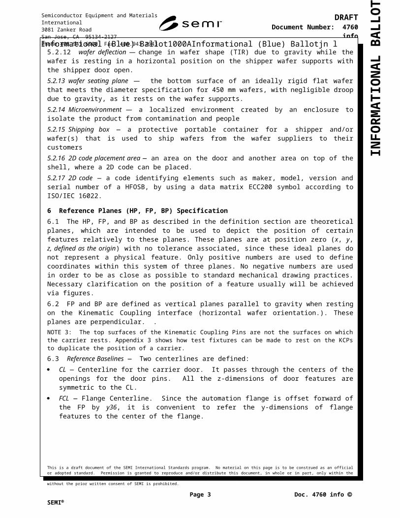
6 Reference Planes (HP, FP, BP) Specification6.1 The HP, FP, and BP as described in the definition section are theoretical planes, which are intended to be used to depict the position of certain features relatively to these planes. These planes are at position zero (x, y, z, defined as the origin) with no tolerance associated, since these ideal planes do not represent a physical feature. Only positive numbers are used to define coordinates within this system of three planes. No negative numbers are used in order to be as close as possible to standard mechanical drawing practices. Necessary clarification on the position of a feature usually will be achieved via figures.6.2 FP and BP are defined as vertical planes parallel to gravity when resting on the Kinematic Coupling interface (horizontal wafer orientation.). These planes are perpendicular. .3: The top surfaces of the Kinematic Coupling Pins are not the surfaces on which the carrier rests. Appendix 3 shows how test fixtures can be made to rest on the KCPs to duplicate the position of a carrier. 6.3 Reference Baselines — Two centerlines are defined: CL — Centerline for the carrier door. It passes through the centers of the openings for the door pins. All the z-
dimensions of door features are symmetric to the CL. FCL — Flange Centerline. Since the automation flange is offset forward of the FP by y36, it is convenient to
refer the y-dimensions of flange features to the center of the flange.
This is a draft document of the SEMI International Standards program. No material on this page is to be construed as an official or adopted standard. Permission is granted to reproduce and/or distribute this document, in whole or in part, only within the scope of SEMI International Standards committee (document development) activity. All other reproduction and/or distribution without the prior written consent of SEMI is prohibited.
Page 2 Doc. 4760 info SEMI
Semiconductor Equipment and Materials International3081 Zanker RoadSan Jose, CA 95134-2127Phone:408.943.6900 Fax: 408.943.7943
DRAFTDocument Number: 4760 info
Date: 2009/08/13

INFO
RM
ATIO
NA
L B
ALL
OT
Informational (Blue) Ballot1000AInformational (Blue) Ballotjn l
Figure 1 (Design A)Overall Views of 450 HFOSB - Design A
7 Shipper Envelope 7.1 The overall dimensions of the 450 HFOSB, (x1), (y1), and (z1), are given as reference dimensions because they are derived from other dimensions. (x1) ≤ x2 + x2 plus tolerances (y1) ≤ y2 + y4 plus tolerances (z1) ≤ x8 + z12plus tolerances
8 Features for Automated Handling 8.1 Automation Flange — On top of the 450 HFOSB is an automation flange for manipulating the carrier. See Figure 2 (top view) and Figures 3, 4 & 5 (sections).
8.1.1 The Automation Flange shall extend front and back from its center (from the FCL) by y3, and shall extend to each side by x3. The neck below the flange shall extend x34 to each side of the BP, and by y56 and y37 in front of the FP.
8.1.2 The Automation Flange has a pattern of notches on all sides. Notches on the front and back have a depth of y31 and those on the sides shall have a depth of x56. The notches shall have an angle of θ4. The four corners shall have chamfers with size of x32 and y28. The flange shall have a centering feature at the intersection of the BP and FCL. The centering feature shall have a depth of z2 and diameter of d3 at the top surface. The side of the centering feature shall have an angle of θ5.
8.1.3 The Automation Flange shall have a thickness of z13, and the shipper shall have no obstructions around the flange for a height of z9, except for the door frame as shown by y30 in Figure 4.
This is a draft document of the SEMI International Standards program. No material on this page is to be construed as an official or adopted standard. Permission is granted to reproduce and/or distribute this document, in whole or in part, only within the scope of SEMI International Standards committee (document development) activity. All other reproduction and/or distribution without the prior written consent of SEMI is prohibited.
Page 3 Doc. 4760 info SEMI
Semiconductor Equipment and Materials International3081 Zanker RoadSan Jose, CA 95134-2127Phone:408.943.6900 Fax: 408.943.7943
DRAFTDocument Number: 4760 info
Date: 2009/08/13
INFO
RM
ATIO
NA
L B
ALL
OT
Informational (Blue) Ballot1000AInformational (Blue) Ballotjn l8.1.4 The Automation Flange shall be located forward of the FP by (y36), the orientation and location are constrained by the values and tolerances of x4 and y40. See Figure 5.
Figure 2 (Design A)Automation Flange – Top View
Figure 3 (Design A) Automation Flange Section at BP
This is a draft document of the SEMI International Standards program. No material on this page is to be construed as an official or adopted standard. Permission is granted to reproduce and/or distribute this document, in whole or in part, only within the scope of SEMI International Standards committee (document development) activity. All other reproduction and/or distribution without the prior written consent of SEMI is prohibited.
Page 4 Doc. 4760 info SEMI
Semiconductor Equipment and Materials International3081 Zanker RoadSan Jose, CA 95134-2127Phone:408.943.6900 Fax: 408.943.7943
DRAFTDocument Number: 4760 info
Date: 2009/08/13
Right Front Left Front

INFO
RM
ATIO
NA
L B
ALL
OT
Informational (Blue) Ballot1000AInformational (Blue) Ballotjn l
Figure 4 - (Design A) Shipper Section at BP
This is a draft document of the SEMI International Standards program. No material on this page is to be construed as an official or adopted standard. Permission is granted to reproduce and/or distribute this document, in whole or in part, only within the scope of SEMI International Standards committee (document development) activity. All other reproduction and/or distribution without the prior written consent of SEMI is prohibited.
Page 5 Doc. 4760 info SEMI
Semiconductor Equipment and Materials International3081 Zanker RoadSan Jose, CA 95134-2127Phone:408.943.6900 Fax: 408.943.7943
DRAFTDocument Number: 4760 info
Date: 2009/08/13
See Figure 3
See Figure 26See Figure 15
Left Right
See Figure 25
See Figure 30

INFO
RM
ATIO
NA
L B
ALL
OT
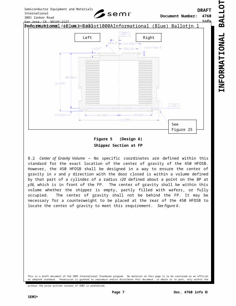
Informational (Blue) Ballot1000AInformational (Blue) Ballotjn lFigure 5 (Design A)Shipper Section at FP
8.2 Center of Gravity Volume ― No specific coordinates are defined within this standard for the exact location of the center of gravity of the 450 HFOSB. However, the 450 HFOSB shall be designed in a way to ensure the center of gravity in x and y direction with the door closed is within a volume defined by that part of a cylinder of a radius r20 defined about a point on the BP at y36, which is in front of the FP. The center of gravity shall be within this volume whether the shipper is empty, partly filled with wafers, or fully occupied. The center of gravity shall not be behind the FP. It may be necessary for a counterweight to be placed at the rear of the 450 HFOSB to locate the center of gravity to meet this requirement. See Figure 6.
Figure 6 (Design A)Automation Flange Location
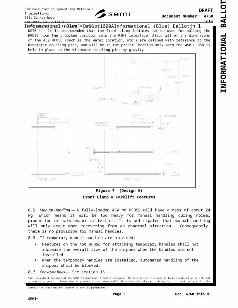
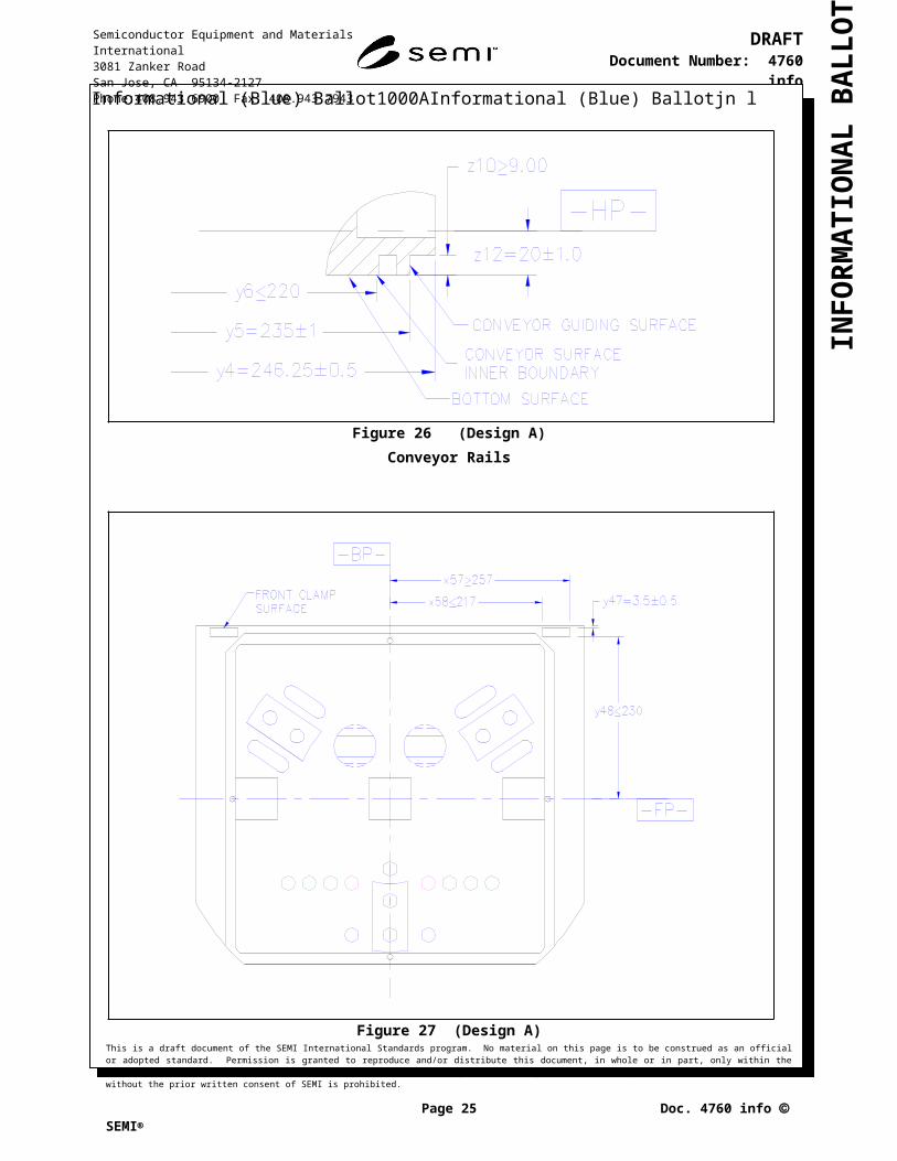
8.3 Forklift Feature — The 450 HFOSB shall have features on the sides for handling by forklift, shown in Figure 7. The forklift feature includes a notched indentation for a pin to retain the carrier on the forklift.
8.3.1 On each side of the carrier, there shall be an opening to the rear extending vertically from z51 to z39, and forward to y45. The surface at z39 shall extend from y45 to y46. There shall be no obstruction at the top of the opening to the rear of y46. The surface at z39 shall extend from x54 to the outside of the shipper. There shall be notches at the FP with a height of z40, a depth of x55 and an angle of θ6.
8.4 Front Clamp Features — The 450 HFOSB shall have provision for being clamped at the front of the shipper.
8.4.1 There shall be two front clamping features on the top of the shipper. Each is a rectangular depression with a depth of z5, and is bounded by x52 & x53, and by y43 & y44. See Figure 7.
8.4.2 There shall be two front clamping features on the bottom of the shipper. They shall be rectangular depression with a depth of z36 and be bounded by x57 & x58, and by y47 & y48. See Figure 27.
This is a draft document of the SEMI International Standards program. No material on this page is to be construed as an official or adopted standard. Permission is granted to reproduce and/or distribute this document, in whole or in part, only within the scope of SEMI International Standards committee (document development) activity. All other reproduction and/or distribution without the prior written consent of SEMI is prohibited.
Page 6 Doc. 4760 info SEMI
Semiconductor Equipment and Materials International3081 Zanker RoadSan Jose, CA 95134-2127Phone:408.943.6900 Fax: 408.943.7943
DRAFTDocument Number: 4760 info
Date: 2009/08/13
LeftRight

INFO
RM
ATIO
NA
L B
ALL
OT
Informational (Blue) Ballot1000AInformational (Blue) Ballotjn l4: It is recommended that the front clamp features not be used for pulling the HFOSB from the undocked position into the FIMS interface. Also, all of the dimensions of the 450 HFOSB (such as the wafer location, etc.) are defined with reference to the kinematic coupling pins, and will be in the proper location only when the 450 HFOSB is held in place on the kinematic coupling pins by gravity.
Figure 7
(Design A)Front Clamp & Forklift Features
8.5 Manual Handling — A fully-loaded 450 mm HFOSB will have a mass of about 24 kg, which means it will be too heavy for manual handling during normal production or maintenance activities. It is anticipated that manual handling will only occur when recovering from an abnormal situation. Consequently, there is no provision for manual handles.8.6 If temporary manual handles are provided:
Features on the 450 HFOSB for attaching temporary handles shall not increase the overall size of the shipper when the handles are not installed.
When the temporary handles are installed, automated handling of the shipper shall be blocked.8.7 Conveyor Rails — See section 15.
9 Requirements for Kinematic Coupling Pins 9.1 Kinematic Coupling Pin Shape — The physical alignment interface on the bottom of the carrier consists of features (specified in § 10) that mate with six pins underneath. As shown in Figure 8 and defined in Table 1, each pin is radially symmetric about its vertical center axis line and can be seen as the intersection of a cylinder of radius r1 and a sphere of radius r4 (which establishes the tip of the pin and might contact a flat plate). The radius r4 is centered on the axis of symmetry at a height z3 below the HP. An additional radius r3 establishes the contact with
This is a draft document of the SEMI International Standards program. No material on this page is to be construed as an official or adopted standard. Permission is granted to reproduce and/or distribute this document, in whole or in part, only within the scope of SEMI International Standards committee (document development) activity. All other reproduction and/or distribution without the prior written consent of SEMI is prohibited.
Page 7 Doc. 4760 info SEMI
Semiconductor Equipment and Materials International3081 Zanker RoadSan Jose, CA 95134-2127Phone:408.943.6900 Fax: 408.943.7943
DRAFTDocument Number: 4760 info
Date: 2009/08/13
INFO
RM
ATIO
NA
L B
ALL
OT
Informational (Blue) Ballot1000AInformational (Blue) Ballotjn lthe angled mating groove surface on the carrier. The center of the radius r3 is defined by the intersection of a vertical plane through the axis of symmetry of the pin with the horizontal circle of radius r2 at the height z4 below the HP. A blend radius of r5 is applied at the intersection of r1 and r3, and at the intersection of r3 and r4. Ra1 is the surface finish roughness, as defined by ISO 4287, of all features given by r1, r3, r4, and r5. Dimensions r2, z3, and z4 have zero tolerance because they only define offsets and not physical features.9.2 Kinematic Coupling Pin Locations — The KC pins are arranged in three sets with two pins in each set, as shown in Figure 11. The outer pins of each set are designated the primary pins for use on a load port or vehicle nest, and the inner pins are designated the secondary pins for use on a robotic arm used to pick up the carrier. The rear pins (farthest from the door) are located on the BP, at a distance from the FP of y18 for the secondary pin and y15 for the primary pin. The front primary pins are located at a distance of y16 from the FP, symmetric across the BP with distance x18 from the BP. The front secondary pins are located at a distance of y17 from the FP, symmetric across the BP with distance x19 from the BP. For reference only, the front kinematic coupling pins are located symmetrically with respect to the BP at an angle of θ2, and circumferentially equidistant on a circle about the origin with radius r22 for the primary kinematic coupling pins and radius r26 for the secondary kinematic coupling pins. For reference only, the rear primary kinematic pin is located on the BP and on a circle with radius r27, and the secondary rear pin is located on the BP and on a circle with radius r16. See Figure 11.
Figure 8 Kinematic Coupling Pin
10 Requirements for Kinematic Coupling Groove In order to achieve the proper lead-in value of r15 and control contact pressures, certain characteristics of the kinematic groove surface on the bottom of the 450 HFOSB are described in this section and shown in Figure 9. 10.1 Kinematic Coupling Groove Locations — Grooves shall be provided to capture both primary and secondary pins locations. The centerlines of the grooves are located along radii passing through the kinematic pin locations from the origin. The rear groove has its centerline along the BP, while the two front grooves have their centerlines at the angle θ2 with respect to the FP.10.2 Kinematic Coupling Groove Shape and Finish — When viewed along the axis of symmetry of the groove (parallel to the HP), the dihedral angle of each wall shall be θ1 to the vertical. The height of the groove at the opening shall be z12 beneath the HP. This should result in an effective half-width of r34 at the mouth of the groove. 10.3 Kinematic Coupling Groove Length — In order to ensure capture of either the primary or secondary K-pin during a physical handoff with an offset (lead-in error) of r15, a minimum groove length is specified. The innermost end of the front KC grooves shall be no farther than r8 from the origin, and the outermost end of the grooves shall be no closer than r24 from the origin. The innermost end of the rear KC groove shall be no farther than r33 from
This is a draft document of the SEMI International Standards program. No material on this page is to be construed as an official or adopted standard. Permission is granted to reproduce and/or distribute this document, in whole or in part, only within the scope of SEMI International Standards committee (document development) activity. All other reproduction and/or distribution without the prior written consent of SEMI is prohibited.
Page 8 Doc. 4760 info SEMI
Semiconductor Equipment and Materials International3081 Zanker RoadSan Jose, CA 95134-2127Phone:408.943.6900 Fax: 408.943.7943
DRAFTDocument Number: 4760 info
Date: 2009/08/13

INFO
RM
ATIO
NA
L B
ALL
OT
Informational (Blue) Ballot1000AInformational (Blue) Ballotjn lthe origin, and the outermost end of the groove shall be no less than r9 from the origin. The KC grooves shall not interfere with the edge of the conveyor rail or other exclusion features. See Figures 10 & 11.
Figure 9
Kinematic Coupling Groove
Figure 10 Kinematic Coupling Offset
This is a draft document of the SEMI International Standards program. No material on this page is to be construed as an official or adopted standard. Permission is granted to reproduce and/or distribute this document, in whole or in part, only within the scope of SEMI International Standards committee (document development) activity. All other reproduction and/or distribution without the prior written consent of SEMI is prohibited.
Page 9 Doc. 4760 info SEMI
Semiconductor Equipment and Materials International3081 Zanker RoadSan Jose, CA 95134-2127Phone:408.943.6900 Fax: 408.943.7943
DRAFTDocument Number: 4760 info
Date: 2009/08/13
INFO
RM
ATIO
NA
L B
ALL
OT
Informational (Blue) Ballot1000AInformational (Blue) Ballotjn l
Figure 11 (Design A) Bottom View – Kinematic Coupling Pin Locations
11 Requirements for Bottom Surface Features
This is a draft document of the SEMI International Standards program. No material on this page is to be construed as an official or adopted standard. Permission is granted to reproduce and/or distribute this document, in whole or in part, only within the scope of SEMI International Standards committee (document development) activity. All other reproduction and/or distribution without the prior written consent of SEMI is prohibited.
Page 10 Doc. 4760 info SEMI
Semiconductor Equipment and Materials International3081 Zanker RoadSan Jose, CA 95134-2127Phone:408.943.6900 Fax: 408.943.7943
DRAFTDocument Number: 4760 info
Date: 2009/08/13

INFO
RM
ATIO
NA
L B
ALL
OT
Informational (Blue) Ballot1000AInformational (Blue) Ballotjn l
Figure 12 (Design A)Bottom Features
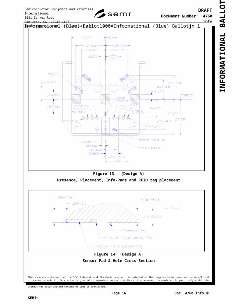
11.1 Presence Sensor Feature
11.1.1 The presence sensing features on the bottom of the 450 HFOSB are designed to provide three flat, opaque areas for sensing. The load port or other systems using KCPs can use the features to determine that a carrier is present, even if misplaced (see the discussion in the Related Information). The features consist of three flat, opaque areas centered along the BP of the carrier within the conveyor rails and extending y21 to the front and rear of the FP. The center area extends x22 to each side of the BP, and the outer areas extend from x20 to x9.
11.2 Placement Sensor Features
11.2.1 Placement sensing features are intended to provide defined locations to confirm proper placement of the kinematic coupling grooves onto the kinematic coupling pins. These consist of a set of four elongated and three circular flat areas located. The elongated flat areas are located symmetrically to the front KC pins, with the outer center at approximately the same distance from the origin (at x21 and y22), The distance from the outer to inner centers is approximately the same as the distance between the primary and secondary KC pins. Two of the circular flat areas” Are located on either side of the rear secondary KC pin, and the third is in front of the rear KC pins, for use with forklifts. The flat areas shall be at a height of z23. Because the KC pins are not symmetrical, this configuration allows fail-safe sensing of the carrier placement. See Figure 13.
11.3 Info Pads & Mechanical Lockout Features
11.3.1 The info pads and mechanical lockout features of the 450 HFOSB are located symmetrically about the BP, with one row of three info pads and one mechanical lockout feature on each side. From the shipper side, there is no difference between the info pads and mechanical lockout features. On the load port side, the optional mechanical lockout pins would be separate from the sensing info pads. As with the placement sensing pads, the info pad features have a radius of r21 mm (flat or hole per customer option). The flat surface shall be at z50 below the HP, (with a more relaxed tolerance than z23). Hole “depth” shall be at z24. For the mechanical lockout feature, the flat must be capable of supporting a fully loaded HFOSB
This is a draft document of the SEMI International Standards program. No material on this page is to be construed as an official or adopted standard. Permission is granted to reproduce and/or distribute this document, in whole or in part, only within the scope of SEMI International Standards committee (document development) activity. All other reproduction and/or distribution without the prior written consent of SEMI is prohibited.
Page 11 Doc. 4760 info SEMI
Semiconductor Equipment and Materials International3081 Zanker RoadSan Jose, CA 95134-2127Phone:408.943.6900 Fax: 408.943.7943
DRAFTDocument Number: 4760 info
Date: 2009/08/13

INFO
RM
ATIO
NA
L B
ALL
OT
Informational (Blue) Ballot1000AInformational (Blue) Ballotjn l11.3.2 The info pads and mechanical lockout features are located y24 mm from the FP, and symmetrically about the BP at distances of x24 mm, x25 mm, x26 mm, and x27 mm from the BP. The two features nearest the FP are reserved for mechanical lockout; the other six are reserved for info sensors only (no mechanical lockout pins). The lockout pads are numbered (1 & 2) and the Info Pads are lettered (A thru F) to highlight that they are not intended to be interchangeable.
Figure 13 (Design A)Presence, Placement, Info-Pads and RFID tag placement
This is a draft document of the SEMI International Standards program. No material on this page is to be construed as an official or adopted standard. Permission is granted to reproduce and/or distribute this document, in whole or in part, only within the scope of SEMI International Standards committee (document development) activity. All other reproduction and/or distribution without the prior written consent of SEMI is prohibited.
Page 12 Doc. 4760 info SEMI
Semiconductor Equipment and Materials International3081 Zanker RoadSan Jose, CA 95134-2127Phone:408.943.6900 Fax: 408.943.7943
DRAFTDocument Number: 4760 info
Date: 2009/08/13

INFO
RM
ATIO
NA
L B
ALL
OT
Informational (Blue) Ballot1000AInformational (Blue) Ballotjn lFigure 14 (Design A)
Sensor Pad & Hole Cross-Section
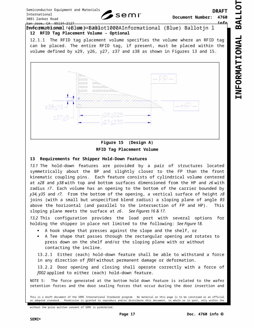
12 RFID Tag Placement Volume - Optional12.1.1 The RFID tag placement volume specifies the volume where an RFID tag can be placed. The entire RFID tag, if present, must be placed within the volume defined by x29, y26, y27, z37 and z38 as shown in Figures 13 and 15.
Figure 15 (Design A)RFID Tag Placement Volume
13 Requirements for Shipper Hold-Down Features13.1 The hold-down features are provided by a pair of structures located symmetrically about the BP and slightly closer to the FP than the front kinematic coupling pins. Each feature consists of cylindrical volume centered at x28 and y38 with top and bottom surfaces dimensioned from the HP and z6 with radius r7. Each volume has an opening to the bottom of the carrier bounded by y34, y35 and r7. From the bottom of the opening, a vertical surface of height z8 joins (with a small but unspecified blend radius) a sloping plane of angle θ3 above the horizontal (and parallel to the intersection of FP and HP). This sloping plane meets the surface at z6. See Figures 16 & 17.13.2 This configuration provides the load port with several options for holding the shipper in place not limited to the following: See Figure 18.
A hook shape that presses against the slope and the shelf, or A Tee shape that passes through the rectangular opening and rotates to press down on the shelf and/or the
sloping plane with or without contacting the incline. 13.2.1 Either (each) hold-down feature shall be able to withstand a force in any direction of f001 without permanent damage or deformation.13.2.2 Door opening and closing shall operate correctly with a force of f002 applied to either (each) hold-down feature.
5: The force generated at the bottom hold down feature is related to the wafer retention forces and the door sealing forces that occur during the door insertion and removal operation. Carrier suppliers should consider the maximum force generated in their shipper design when designing the carrier’s hold down feature.
This is a draft document of the SEMI International Standards program. No material on this page is to be construed as an official or adopted standard. Permission is granted to reproduce and/or distribute this document, in whole or in part, only within the scope of SEMI International Standards committee (document development) activity. All other reproduction and/or distribution without the prior written consent of SEMI is prohibited.
Page 13 Doc. 4760 info SEMI
Semiconductor Equipment and Materials International3081 Zanker RoadSan Jose, CA 95134-2127Phone:408.943.6900 Fax: 408.943.7943
DRAFTDocument Number: 4760 info
Date: 2009/08/13

INFO
RM
ATIO
NA
L B
ALL
OT
Informational (Blue) Ballot1000AInformational (Blue) Ballotjn l
Figure 16 (Design A) Hold-Down Feature Locations
Figure 17 (Design A) Hold-Down Section at x28=50 mm
This is a draft document of the SEMI International Standards program. No material on this page is to be construed as an official or adopted standard. Permission is granted to reproduce and/or distribute this document, in whole or in part, only within the scope of SEMI International Standards committee (document development) activity. All other reproduction and/or distribution without the prior written consent of SEMI is prohibited.
Page 14 Doc. 4760 info SEMI
Semiconductor Equipment and Materials International3081 Zanker RoadSan Jose, CA 95134-2127Phone:408.943.6900 Fax: 408.943.7943
DRAFTDocument Number: 4760 info
Date: 2009/08/13

INFO
RM
ATIO
NA
L B
ALL
OT
Informational (Blue) Ballot1000AInformational (Blue) Ballotjn l
Figure 18 (Design A) Hold-Down Devices
14 Requirements for Carrier Door14.1 The HFOSB is not intended to be opened with the wafers in a vertical orientation. 14.2 The shipper door is on the front of the 450 HFOSB. The door and its frame must be designed to mate with a load port that conforms to the Mechanical Interface Specification for 450 mm Load Port. The HFOSB door and its frame must have surfaces that mate with seal areas, the HFOSB door sensing area, and reserved spaces for vacuum application. See Figure 19.14.3 The spaces for vacuum application include the four of the circles bounded by r28 and located at x49 & z31. The vacuum pad areas, door seal areas, frame seal areas and door sense areas shall be at a distance of y4 from the facial plane when the door is closed and latched. No surface on the HFOSB door may project further from the facial plane than these areas and the reserved spaces. 14.4 The door of the HFOSB must also be designed so that when the HFOSB is pressed against the FIMS port, both latch keys on the port are inserted to their full length there is clearance of y39. Furthermore, when the latch keys are turned more than 45° toward the position that unlocks the HFOSB door from the HFOSB, the latch key holes on the door must be such that the door is not removable from the latch keys.14.5 To allow for unobstructed latch key rotation, the thickness of the outer panel of the carrier door in the area defined by r23 shall be y10. Clearance of y39 shall be provided for latch keys at x46. Clearance of y40 shall be provided for door pins at x45. The latchkeys and door pins shall be located on the centerline (CL). See Figure 22. 14.6 HFOSB door features are symmetrical about the CL. Features other than the openings for Frame Pins and Door Pins are symmetrical about the BP.14.7 The openings for the door pins are circular on the left side with diameter d4, and are slots on the right side. See Figure 23.14.8 The openings for the frame pins are circular on the left side with diameter d5, and are slots on the right side.
This is a draft document of the SEMI International Standards program. No material on this page is to be construed as an official or adopted standard. Permission is granted to reproduce and/or distribute this document, in whole or in part, only within the scope of SEMI International Standards committee (document development) activity. All other reproduction and/or distribution without the prior written consent of SEMI is prohibited.
Page 15 Doc. 4760 info SEMI
Semiconductor Equipment and Materials International3081 Zanker RoadSan Jose, CA 95134-2127Phone:408.943.6900 Fax: 408.943.7943
DRAFTDocument Number: 4760 info
Date: 2009/08/13

INFO
RM
ATIO
NA
L B
ALL
OT
Informational (Blue) Ballot1000AInformational (Blue) Ballotjn l
Figure 19 (Design A) 450 HFOSB Door Features
14.9 The frame seal area is bounded by x11 & x64on the sides, by z27& z34on the top, and by z28 & z44on the bottom. There is a blend radius r30 & r36 at the corners. 14.10 The door seal area is bounded by x47& x48 on the sides, and by z32 & z33 on the top and bottom. There are blend radii of r31 & r32 at the outer and inner edges respectively.
Figure 20
(Design A)Shipper Door Frame
This is a draft document of the SEMI International Standards program. No material on this page is to be construed as an official or adopted standard. Permission is granted to reproduce and/or distribute this document, in whole or in part, only within the scope of SEMI International Standards committee (document development) activity. All other reproduction and/or distribution without the prior written consent of SEMI is prohibited.
Page 16 Doc. 4760 info SEMI
Semiconductor Equipment and Materials International3081 Zanker RoadSan Jose, CA 95134-2127Phone:408.943.6900 Fax: 408.943.7943
DRAFTDocument Number: 4760 info
Date: 2009/08/13
INFO
RM
ATIO
NA
L B
ALL
OT
Informational (Blue) Ballot1000AInformational (Blue) Ballotjn l
Figure 21 (Design A)Carrier Door
Figure 22 (Design A)Section at Door Centerline - Looking Down on the Left Side
This is a draft document of the SEMI International Standards program. No material on this page is to be construed as an official or adopted standard. Permission is granted to reproduce and/or distribute this document, in whole or in part, only within the scope of SEMI International Standards committee (document development) activity. All other reproduction and/or distribution without the prior written consent of SEMI is prohibited.
Page 17 Doc. 4760 info SEMI
Semiconductor Equipment and Materials International3081 Zanker RoadSan Jose, CA 95134-2127Phone:408.943.6900 Fax: 408.943.7943
DRAFTDocument Number: 4760 info
Date: 2009/08/13
See Figure 23
INFO
RM
ATIO
NA
L B
ALL
OT
Informational (Blue) Ballot1000AInformational (Blue) Ballotjn l
Figure 23 (Design A) Frame Pin and Door Pin Area - Right Side
14.11 Front Clamp Features — See section 8.4. Figure 7 shows the top front clamp features and Figure 27 shows the bottom front clamp features. 6: It is recommended that the front clamp features not be used for pulling the HFOSB from the undocked position into the FIMS interface. Also, all of the dimensions of the 450 HFOSB (such as the wafer location, etc.) are defined with reference to the kinematic coupling pins, and will be in the proper location only when the 450 HFOSB is held in place on the kinematic coupling pins by gravity.14.12 Door Closing Force — The force required to push the carrier door into the carrier shell to its fully seated position is f234. The application of f234 to the door shall push the door fully closed, so that the outermost point of the outer surface of the door is less than or equal to y4 from the BP. With the door in this position, the latches shall operate without exceeding the torque limit f230.14.13 Thickness of Door (y9) — y58 See Figure 7 Section 8 7: Shipper suppliers should design their products to keep this force required to close as small as possible to ensure no damage will occur to wafers upon opening and closing the door.14.14 Latch Torque — The maximum torque required to turn each of the latch mechanisms individually on the carrier door (to which the latch keys of a load port will engage with) is f230.14.15 See Related Information R1-7 for more discussion.
15 Requirements for Conveyor RailsThis section specifies certain aspects of the 450 HFOSB that define the conveyor rails, their exclusion areas, and relationships to other features.15.1 Conveyor Rail Surface Dimensions — The conveying surface extends below the HP, as shown in Figures 25 and 26. The bottom view is given in Figure 24. The conveyor rail surfaces are meant to provide smooth, continuous surfaces symmetric to the origin. The inner edges of the conveying surfaces are bounded by x6 and y6, and the outer guiding edges of the conveying surfaces are defined by x5 and y5. A blend radius r11 connects the corners of the edges, and the four outer corners are bounded by radius r35. The conveying surface forms a plane at a distance z11 below the HP. 15.2 Conveyor Rail Cylindrical Forklift Pin Holes – Holes are provided on all four conveyor rails, defining cylindrical volumes on the FP. The holes (cylinders) are of diameter d1, centered on the FP at distances x37and on the BP at y32. The depth of the holes is z46.15.3 Conveyor Guiding Surface —. The external edges of the conveyor rails will provide a physical conveyor guiding surface consisting of a vertical edge with height of z10 above the conveying surface. No part of the HFOSB
This is a draft document of the SEMI International Standards program. No material on this page is to be construed as an official or adopted standard. Permission is granted to reproduce and/or distribute this document, in whole or in part, only within the scope of SEMI International Standards committee (document development) activity. All other reproduction and/or distribution without the prior written consent of SEMI is prohibited.
Page 18 Doc. 4760 info SEMI
Semiconductor Equipment and Materials International3081 Zanker RoadSan Jose, CA 95134-2127Phone:408.943.6900 Fax: 408.943.7943
DRAFTDocument Number: 4760 info
Date: 2009/08/13

INFO
RM
ATIO
NA
L B
ALL
OT
Informational (Blue) Ballot1000AInformational (Blue) Ballotjn lmay occupy the volume outside of the conveyor guiding surface. Note that r35 applies to the guiding surface while r10 applies to parts of the carrier that are above z10.
15.3.1 The conveyor guiding surfaces shall be opaque for the purpose of presence sensing.
Figure 24 (Design A)Conveyor Rail Locations
This is a draft document of the SEMI International Standards program. No material on this page is to be construed as an official or adopted standard. Permission is granted to reproduce and/or distribute this document, in whole or in part, only within the scope of SEMI International Standards committee (document development) activity. All other reproduction and/or distribution without the prior written consent of SEMI is prohibited.
Page 19 Doc. 4760 info SEMI
Semiconductor Equipment and Materials International3081 Zanker RoadSan Jose, CA 95134-2127Phone:408.943.6900 Fax: 408.943.7943
DRAFTDocument Number: 4760 info
Date: 2009/08/13

INFO
RM
ATIO
NA
L B
ALL
OT
Informational (Blue) Ballot1000AInformational (Blue) Ballotjn l
Figure 25 (Design A)Conveyor Rails
Figure 26 (Design A)Conveyor Rails
This is a draft document of the SEMI International Standards program. No material on this page is to be construed as an official or adopted standard. Permission is granted to reproduce and/or distribute this document, in whole or in part, only within the scope of SEMI International Standards committee (document development) activity. All other reproduction and/or distribution without the prior written consent of SEMI is prohibited.
Page 20 Doc. 4760 info SEMI
Semiconductor Equipment and Materials International3081 Zanker RoadSan Jose, CA 95134-2127Phone:408.943.6900 Fax: 408.943.7943
DRAFTDocument Number: 4760 info
Date: 2009/08/13

INFO
RM
ATIO
NA
L B
ALL
OT
Informational (Blue) Ballot1000AInformational (Blue) Ballotjn l
Figure 27 (Design A)Front Clamps
16 Requirements for Wafer Support Features 16.1.1 Location of wafer contacts — 450 mm wafers shall be handled or contacted within an exclusion area that extends 2 mm in from the edges of the wafers. Dimensions have been selected to eliminate backside contact more than 2 mm away from the edge of a wafer, when it is within either the wafer pick-up volume or wafer set down volume. See Figures 28, 29 & 30.16.1.2 The wafer support areas are bounded by r35 & r36 towards the front and rear, by x13 on the inside and x50 on the outside. If the wafer supports are moved out from x13 the wafer deflection will increase. See Related Information 1 for discussion of wafer sag. At the rear of the shipper, an optional additional area, bounded by x14, and between and y11 & y19, may be used for wafer support. 16.1.3 The shipper shall have features to constrain the wafer along all axes so the wafer will be within the wafer pick-up volume after the door is opened. See Figures 31 & 32.
This is a draft document of the SEMI International Standards program. No material on this page is to be construed as an official or adopted standard. Permission is granted to reproduce and/or distribute this document, in whole or in part, only within the scope of SEMI International Standards committee (document development) activity. All other reproduction and/or distribution without the prior written consent of SEMI is prohibited.
Page 21 Doc. 4760 info SEMI
Semiconductor Equipment and Materials International3081 Zanker RoadSan Jose, CA 95134-2127Phone:408.943.6900 Fax: 408.943.7943
DRAFTDocument Number: 4760 info
Date: 2009/08/13

INFO
RM
ATIO
NA
L B
ALL
OT
Informational (Blue) Ballot1000AInformational (Blue) Ballotjn lFigure 28
(Design A) HFOSB Section (Between Wafer Supports)
This is a draft document of the SEMI International Standards program. No material on this page is to be construed as an official or adopted standard. Permission is granted to reproduce and/or distribute this document, in whole or in part, only within the scope of SEMI International Standards committee (document development) activity. All other reproduction and/or distribution without the prior written consent of SEMI is prohibited.
Page 22 Doc. 4760 info SEMI
Semiconductor Equipment and Materials International3081 Zanker RoadSan Jose, CA 95134-2127Phone:408.943.6900 Fax: 408.943.7943
DRAFTDocument Number: 4760 info
Date: 2009/08/13

INFO
RM
ATIO
NA
L B
ALL
OT
Informational (Blue) Ballot1000AInformational (Blue) Ballotjn l
Figure 29 (Design A)Wafer Support Area
Figure 30 (Design A)Wafer Slots
This is a draft document of the SEMI International Standards program. No material on this page is to be construed as an official or adopted standard. Permission is granted to reproduce and/or distribute this document, in whole or in part, only within the scope of SEMI International Standards committee (document development) activity. All other reproduction and/or distribution without the prior written consent of SEMI is prohibited.
Page 23 Doc. 4760 info SEMI
Semiconductor Equipment and Materials International3081 Zanker RoadSan Jose, CA 95134-2127Phone:408.943.6900 Fax: 408.943.7943
DRAFTDocument Number: 4760 info
Date: 2009/08/13

INFO
RM
ATIO
NA
L B
ALL
OT
Informational (Blue) Ballot1000AInformational (Blue) Ballotjn l
Figure 31 (Design A)Wafer Pick-Up Volume
Figure 32 (Design A)Wafer Pick-Up Side View
This is a draft document of the SEMI International Standards program. No material on this page is to be construed as an official or adopted standard. Permission is granted to reproduce and/or distribute this document, in whole or in part, only within the scope of SEMI International Standards committee (document development) activity. All other reproduction and/or distribution without the prior written consent of SEMI is prohibited.
Page 24 Doc. 4760 info SEMI
Semiconductor Equipment and Materials International3081 Zanker RoadSan Jose, CA 95134-2127Phone:408.943.6900 Fax: 408.943.7943
DRAFTDocument Number: 4760 info
Date: 2009/08/13

INFO
RM
ATIO
NA
L B
ALL
OT
Informational (Blue) Ballot1000AInformational (Blue) Ballotjn l
Figure 33 (Design A)Wafer Set-Down Volume
Figure 34 (Design A)Wafer Set-Down Side View
This is a draft document of the SEMI International Standards program. No material on this page is to be construed as an official or adopted standard. Permission is granted to reproduce and/or distribute this document, in whole or in part, only within the scope of SEMI International Standards committee (document development) activity. All other reproduction and/or distribution without the prior written consent of SEMI is prohibited.
Page 25 Doc. 4760 info SEMI
Semiconductor Equipment and Materials International3081 Zanker RoadSan Jose, CA 95134-2127Phone:408.943.6900 Fax: 408.943.7943
DRAFTDocument Number: 4760 info
Date: 2009/08/13
INFO
RM
ATIO
NA
L B
ALL
OT
Informational (Blue) Ballot1000AInformational (Blue) Ballotjn l
Figure 35 (Design A)Wafer Extraction Volume
Figure 36 (Design A)Wafer Extraction Side View
16.2 Requirements for Wafer Slot Pitch 16.2.1 Vertical Dimensions — Figures 4 & 5show the vertical dimensions of the shipper. Note that z14 (the height of the bottom nominal wafer seating plane above the horizontal datum plane) and z17 (the distance between adjacent nominal wafer seating planes) are given as absolute distances with no tolerance. This means that the sum of actual height variations in the shipper from the kinematic coupling to the supporting features holding each wafer shall be contained within the tolerance of z21 with no further stack-up at each higher wafer. z15 specifies the space reserved for end effectors below the first wafer. The method for meeting these requirements is left up to the shipper supplier. As wafer supports are moved farther apart from the BP, the wafer deflection under gravity will increase. The wafer
This is a draft document of the SEMI International Standards program. No material on this page is to be construed as an official or adopted standard. Permission is granted to reproduce and/or distribute this document, in whole or in part, only within the scope of SEMI International Standards committee (document development) activity. All other reproduction and/or distribution without the prior written consent of SEMI is prohibited.
Page 26 Doc. 4760 info SEMI
Semiconductor Equipment and Materials International3081 Zanker RoadSan Jose, CA 95134-2127Phone:408.943.6900 Fax: 408.943.7943
DRAFTDocument Number: 4760 info
Date: 2009/08/13

INFO
RM
ATIO
NA
L B
ALL
OT
Informational (Blue) Ballot1000AInformational (Blue) Ballotjn lpitch budget assumes that wafer deflection will be no more than 0.50 mm above end effector, so if wafer supports are designed to allow more than 0.50 mm of deflection, the thickness of the wafer support, (z17 – z16) or its tolerance (z21) needs to be reduced accordingly. See also Figure 30.16.2.2 Wafer Set-Down Volume ― The open space for the wafer set-down volume consists of a cylindrical section with radius r12 and a vertical axis y14 in front of the origin. The bottom of this cylindrical section is z49 above the nominal wafer seating plane and its height is z22. See Figures 33 & 34.16.2.3 The implications of the tolerance on r12 for wafer positioning are as follows. The wafers shall be placed in the carrier within a circle of radius corresponding to the smaller bound on r12 to avoid touching the edge of the wafer to the side of the carrier. Once the wafer has been placed, the carrier shall not allow a wafer to move outside of a circle of radius corresponding to the larger bound on r12. There are two exceptions to this limit on wafer movement. When the wafer is pushed toward the rear of the carrier, the location of the wafer is defined by the wafer pick-up volume See figures 31 & 3216.2.4 Wafer Extraction Volume ― The open space for the wafer extraction volume shall include a cylindrical section with radius r18 which has a vertical axis y14 in front of the origin. The vertical cross section at the FP is extended out to the door opening. The bottom of this cylindrical section is z22 above the nominal wafer seating plane and its height is z49. See Figures 35 & 36.16.2.5 The implications of wafer extraction for the definition of dimension r18 are as follows. The carrier shall provide an extra 1 mm of horizontal clearance once the wafer is picked up from wherever it ends up (within the bounds of r12) after transport in the shipper. 16.2.6 If a wafer is placed in the wafer set-down volume and is then pushed toward the rear of the shipper, then the entire bottom of the wafer shall be contained in the wafer pick-up volume. 8: If the wafer is not pushed toward the rear of the shipper, then the wafer may only be somewhere within the wafer extraction volume.16.2.7 Wafer Pick-Up Volume ― The wafer pick-up volume shall be defined by a cylindrical section with radius r13 and a vertical axis at the origin. Its top and bottom are the upper and lower tolerance of z21 around the nominal wafer seating plane. Between the time when the wafer is set down and when it is picked up, including transportation, the wafer shall not be rotated from its wafer set-down position by more than θ7 (6.3 mm along perimeter), nor shall it be displaced from its original slot. See Figures 31 & 32.16.2.8 Wafer Insertion and Extraction — The extraction volume is the maximum space available for a wafer to be moved into or out of the shipper.16.2.9 Wafer Retaining Structure — The slot is usually designed that wafers are suspended in the slot without contacting the surface of the slot for preventing the damage during transportation when HFOSB door is closed. It should be noted that wafer position when door is open may be different than when the door is closed due to the wafer retaining structure.16.2.10 Wafer Retaining — When the HFOSB is closed, the wafers must be retained in the HFOSB to prevent movement during subsequent handling, including shipping. It should be noted that wafers are required to be shipped in a vertical orientation and generally require shipping performance from secondary packaging. It is recommended that this secondary package be designed to allow for automated removal of the HFOSB from the secondary packaging.
17 Requirements for Internal End Effector Exclusion Volume17.1 Internal end effectors reaching into the shipper shall stay between the wafer support areas defined by x13 See Figure 37.17.2 The maximum reach into the carrier is limited by r6, y11, and y19.
This is a draft document of the SEMI International Standards program. No material on this page is to be construed as an official or adopted standard. Permission is granted to reproduce and/or distribute this document, in whole or in part, only within the scope of SEMI International Standards committee (document development) activity. All other reproduction and/or distribution without the prior written consent of SEMI is prohibited.
Page 27 Doc. 4760 info SEMI
Semiconductor Equipment and Materials International3081 Zanker RoadSan Jose, CA 95134-2127Phone:408.943.6900 Fax: 408.943.7943
DRAFTDocument Number: 4760 info
Date: 2009/08/13
INFO
RM
ATIO
NA
L B
ALL
OT
Informational (Blue) Ballot1000AInformational (Blue) Ballotjn l
Figure 37 (Design A)End Effector Exclusion Area
This is a draft document of the SEMI International Standards program. No material on this page is to be construed as an official or adopted standard. Permission is granted to reproduce and/or distribute this document, in whole or in part, only within the scope of SEMI International Standards committee (document development) activity. All other reproduction and/or distribution without the prior written consent of SEMI is prohibited.
Page 28 Doc. 4760 info SEMI
Semiconductor Equipment and Materials International3081 Zanker RoadSan Jose, CA 95134-2127Phone:408.943.6900 Fax: 408.943.7943
DRAFTDocument Number: 4760 info
Date: 2009/08/13
End Effector Boundary Area

INFO
RM
ATIO
NA
L B
ALL
OT
Informational (Blue) Ballot1000AInformational (Blue) Ballotjn l
Table 1 (Design A) Carrier and KC Dimensions Note: All linear dimensions are in mm, all angular dimensions are in degrees.
Symbol Used Figure Value Specified Datum Measured From Feature Measured To
θ1 9 45 ±6 degrees Vertical (BP & FP) Dihedral angle to planar surface of kinematic coupling groove
(θ2) 11 (34.0 degrees) BP Axis of symmetry of front pin-mating groove
θ3 17 30.0 ± 2degrees HP Incline of hold-down feature θ5 5 45 ±0.5 degrees Vertical (BP & FP) Edge of automation flange centering
feature θ4 2 45 ±0.5 degrees Perpendicular to Side surface
of automation flangeSide surfaces of automation flange notches
θ6 7 45 ±0.5degrees FP Side of forklift retainer feature
θ7 not shown ≤1.6 degrees n/a Maximum rotation of any wafer between wafer set-down and wafer pick-up, including door closing, transportation and door opening.
d1 24 8.0 ±0.5 x37, FP and y32, BP Diameter of conveyor rail pin hole(d2) 3 (17) Automation flange centering
feature (BP & FCL)Diameter at bottom of depression
d3 2, 3 51. 0 ±0.5 Automation flange centering feature (BP & FCL)
Diameter at top of depression
d4 21 10.6 x45, CL Diameter of door pin openingd5 20 6.5 ±0.2 x46, CL Diameter of frame pin openingd6 23 6.5 ±0.2 (x40 & x41), CL Diameter of slot for Frame Pind7 23 10.0 (x43 & x42), CL Diameter of slot for Door Pin
f001 13.2. 1 ≥ 175 N Applied at any point, in any direction
Force that the any one hold down feature that the shipper must withstand.
f002 13.2. 2 ≥ 141 N Force applied to hold down feature
Force that shipper must withstand during door opening and closing
f230 14. 14 ≤ 1.7 Nm Latch Key Torque required to operate latches (each latch key)
f234 14. 12 ≤ 227 N Door Force to close shipper door
r1 8 10.0 ±0.025 Centerline of KCP Cylindrical (Side) surface of KCPr2 8 14.0 ± 0 Centerline of KCP Circle to define center of curvature of
KCP contact surfacer3 8 30.0 ±0.05 Circle defined by r2 & z4 Contact surface of KCPr4 8 15.0 ±0.05 Centerline of KCP & z3 Top surface of KCP (sphere)r5 8 2.0 ±0.1 Blend radius Surface between KCP contact surface
and adjacent surfacesr6 28 ≥ 245 Origin Rear boundary of EE exclusion arear7 16 ≥ 30 x26, y29 Cylindrical volume of hold-down
featurer8 11 ≤ 136 Origin Innermost end of Kinematic Coupling
Groove for Front KCPs
This is a draft document of the SEMI International Standards program. No material on this page is to be construed as an official or adopted standard. Permission is granted to reproduce and/or distribute this document, in whole or in part, only within the scope of SEMI International Standards committee (document development) activity. All other reproduction and/or distribution without the prior written consent of SEMI is prohibited.
Page 29 Doc. 4760 info SEMI
Semiconductor Equipment and Materials International3081 Zanker RoadSan Jose, CA 95134-2127Phone:408.943.6900 Fax: 408.943.7943
DRAFTDocument Number: 4760 info
Date: 2009/08/13

INFO
RM
ATIO
NA
L B
ALL
OT
Informational (Blue) Ballot1000AInformational (Blue) Ballotjn lSymbol Used Figure Value Specified Datum Measured From Feature Measured To
r9 11 ≥ 218 Origin Outermost end of Kinematic Coupling Groove for rear KCP
r10 6, 24, 28 ≤ 314 Origin Outer limit of carrier and conveyor rails
r11 24 ≥10 Blend Radius Blend radius of conveyor rail edgesr12 33, 34 227 +1/-0 x=0, y14 Radius of wafer set-down volumer13 31, 32 ≤ 226 Origin Radius of wafer pick-up volume
r15 10 ≥ 15 N/A Lead in: Correctable 450 HFOSB misalignment in any horizontal direction
(r16) 11 (145) Origin Location of Rear Secondary KCPr18 35, 36 ≥ r12 + 1.0 Origin Radius of wafer extraction volumer19* A1-1, A1-2 ≤10 x=190, y=75 Blend radiusr20 6 ≤ 17 BP, y36 Outer surface of cylinder contains the
center of gravity of the shipperr21 13 ≥ 10.0 Center of Info, placement and
Lock-Out padsExtent of pad area
(r22) 11 (206.5) Origin Location of Front Primary KCPsr23 21, 23 ≥ 14 latch key Clearancer24 11 ≥ 231 Origin Outermost end of Kinematic Coupling
Groove for Front KCPs(r25) 11, A1-1 (225) Origin Radius of 450 mm diameter wafer(r26) 11 (160) Origin Location of Front Secondary KCPs(r27) 11 (194) Origin Location of Rear Primary KCPr28 21 ≥ 30 x38,z31 Area reserved for vacuum padsr29 21 ≥ 20 x44, CL & x45, CL Boundary of door sense arear30 20 23.0 Blend radius Corners of door openingr31 21 21.0 Blend radius Corners of doorr32 21 ≥ 19 Blend radius Edge of door seal arear33 11 ≤121 Origin Innermost end of Kinematic Coupling
Groove for Rear KCPsr34 10 ≥ 23.5 KC Groove Centerline Effective half-width of KCP groover35 29 ≥ 200 Origin Inner boundary of wafer supportr36 28 ≥ 229 Origin Inner wall of HFOSB
Ra1 ¶ 9.1 ≤ 0.30 µm n/a Kinematic pin surface finish Roughness per ISO 4287
(x1) 1, 5, 11, 20, 28
(555) n/a Overall width of shipper
x2 6, 7, 20, 28, ≤ 277.5 BP Outer edge of shipperx3 2 300±0.5 Width of automation flangex4 5 150 ±1 BP Edge of automation flange on carrierx5 5, 24,25 235 ± 1 BP Outer edge of side conveyor rail
surfacex6 24 ≤220 BP Inner edge of side conveyor rail
surfacex9 13 ≥ 220 BP Outer Edge of presence sense area
This is a draft document of the SEMI International Standards program. No material on this page is to be construed as an official or adopted standard. Permission is granted to reproduce and/or distribute this document, in whole or in part, only within the scope of SEMI International Standards committee (document development) activity. All other reproduction and/or distribution without the prior written consent of SEMI is prohibited.
Page 30 Doc. 4760 info SEMI
Semiconductor Equipment and Materials International3081 Zanker RoadSan Jose, CA 95134-2127Phone:408.943.6900 Fax: 408.943.7943
DRAFTDocument Number: 4760 info
Date: 2009/08/13

INFO
RM
ATIO
NA
L B
ALL
OT
Informational (Blue) Ballot1000AInformational (Blue) Ballotjn lSymbol Used Figure Value Specified Datum Measured From Feature Measured To
x10 13 193±1 BP Center of placement sense areax11 20, 28, 259 BP Opening for shipper doorx12 28, 37, A1-
2≥ 243. 5 BP Inner edge of EE exclusion area
x13 29, 37, ≥ 135 BP Inner extent of wafer support surface x14 29, 37 ≤ 50 BP Extent of rear wafer support structurex18 11 171.20±0.05 BP Location of front primary KCPx19 11 132.65 ±0.05 BP Location of front secondary KCPx20 13 ≤160 BP Inner edge of side presence sense areax21 13
141±1BP Center of invalid placement sense area
x22 13 ≥30 BP Edge of central presence sense areax23 13 55±1 BP Center of rear placement sense areax24 13 55±1 BP Center of lock-out pad (1 left / 2 right)x25 13 85±1 BP Center of Info Pad (1 left / 4 right)x26 13 115±1 BP Center of Info Pad ( 2 left / 5 right)x27 13 145±1 BP Center of info Pad (3 left / 6 right)x28 16 50 ±0.5 BP Center of hold-down featurex29 13 25±1 BP Side of RFID placement volumex30 2
50±0.5BP Automation Flange Notch
x31 2 60 ±0.38210 ±0.5
BP Automation Flange Notch
x32 212±1
Edge of flange Automation Flange chamfer
x33 2250±0.5
BP Automation Flange notch
x34 5 ≤ 132 BP Side of automation flange neckx37 24
450±1Forklift pin hole
x38 21, 23 ≥ 10 Centered at x44, CL Width of latch key clearancex40 23 ≥1.0 Centered at x41 Length of slot for frame pin x41 23 272 ±0.25 BP Center of opening for frame pin r24x42 23 ≥3.0 Centered at x43 Length of slot for door pinx43 23 220 BP Center of opening for right door pin
r22x44 21,23 142 BP Latch keyx45 21 220 BP Left door pinx46 20 272 ±0.25 BP Left frame pinx47 21 257 BP Side of HFOSB doorx48 21 ≥2 BP door seal widthx49 21 200 BP Space reserved for vacuum padsx50 5, 28 ≥ 229 BP Inner wall of shipperx52 7 ≥ 250 BP Outer side of top front clamping
feature
This is a draft document of the SEMI International Standards program. No material on this page is to be construed as an official or adopted standard. Permission is granted to reproduce and/or distribute this document, in whole or in part, only within the scope of SEMI International Standards committee (document development) activity. All other reproduction and/or distribution without the prior written consent of SEMI is prohibited.
Page 31 Doc. 4760 info SEMI
Semiconductor Equipment and Materials International3081 Zanker RoadSan Jose, CA 95134-2127Phone:408.943.6900 Fax: 408.943.7943
DRAFTDocument Number: 4760 info
Date: 2009/08/13

INFO
RM
ATIO
NA
L B
ALL
OT
Informational (Blue) Ballot1000AInformational (Blue) Ballotjn lSymbol Used Figure Value Specified Datum Measured From Feature Measured To
x53 7 ≤ 210 BP Inner side of top front clamping feature
x54 7 ≤ 260 BP Inner side of optional forklift feature x55 7 14 ± .5 Outer edge of carrier Depth of notch for forkliftx56 2 14 ± .5 edge of automation flange depth of notchesx57 27 ≥257 BP Outer side of bottom front clampx58 27 ≤ 217 BP Inner side of bottom front clampx59 24 470±1 Left side of conveyor guiding
surfaceOpposite side of conveyor guiding surface
x60 24 10 ±0.2 Left side of conveyor guiding surface
Left fork lift hole
x61 13 154 ±1 BP Inner center of placement sense padx62 13 102 ±1 BP Inner center of placement sense padx63 2 150 ±0.5 Right Side of automation
flangeFront Notch
x64 20 ≥275.5 BP Outer side of frame seal areax66 7 276 ±1 BP Outer surface of fork lift feature
(y1) 1, 11, 28, 31, 33, 35
(481.75) n/a Overall depth of shipper
y2 4, 6, 28 ≤ 235 FP Rear of shippery3 2, 3 150 ±0.5
300 ±0.5 Depthof handling flange
4, 6, , 28, 246.25 ±0.5 FP Front surface of shippery5 24, 25, 26 235 ±0.25 FP Outer edge of Front & Rear conveyor
rail surfacey6 24 220 ±0.25 FP Inner edge of Front & Rear conveyor
rail surfacey8 28, 29, 37, ≤ 180 FP Inner extent of IEE exclusion area
between x12 and x13y9 4, 28, 37, ≥ 211.25 FP Inner sealing surface to doory10 22 3.25 ±0.25
3.00±0.25Front surface of door (y4) Space for unobstructed rotation of
latch keys
y11 28, 29, 37 ≥ 200 FP Extent of rear wafer support structurey12 6 162 ±1 FP Front edge of automation flangey14 32 >0, ≤3.0 FP Center of r12y15 11 194 ±0.05 FP Location of Rear Primary KCPy16 11 115.5 ±0.05 FP Location of front primary KCPy17 11 89.5 ±0.05 FP Location of front secondary KCPy18 11 145 ±0.05 FP Location of rear secondary KCPy19 4, 28, 31,
33, 34, 35, 36,
≥ 228 FP Inner extent of IEE exclusion area near rear wafer support structure
y21 13 ≥ 30 FP Edges of side presence sense areay22 13 151 ±1 FP Center of placement NOT sense areay23 13 74 ±1 FP Center of placement sense areay24 13 120 ±1 FP Row of Info and Lock Out padsy25 13 194 ±1 FP Center of rear placement sense areas
This is a draft document of the SEMI International Standards program. No material on this page is to be construed as an official or adopted standard. Permission is granted to reproduce and/or distribute this document, in whole or in part, only within the scope of SEMI International Standards committee (document development) activity. All other reproduction and/or distribution without the prior written consent of SEMI is prohibited.
Page 32 Doc. 4760 info SEMI
Semiconductor Equipment and Materials International3081 Zanker RoadSan Jose, CA 95134-2127Phone:408.943.6900 Fax: 408.943.7943
DRAFTDocument Number: 4760 info
Date: 2009/08/13

INFO
RM
ATIO
NA
L B
ALL
OT
Informational (Blue) Ballot1000AInformational (Blue) Ballotjn lSymbol Used Figure Value Specified Datum Measured From Feature Measured To
y26 4, 13, 15 ≥ 225 FP Front of RFID placement volumey27 4, 13, 15 ≤ 230 FP Rear of RFID placement volumey28 2
12 ±1 Edge of Automation Flange Automation Flange chamfer
y29 290 ±0.5
FP Automation Flange notch
y30 4 ≥ 195.75 FP Back of door flangey31 2
14 ±0.5Edge of automation flange Depth of notches
y32 24450 ±1
FP Front and rear forklift holes
y34 16, 17 90 ±0.5 FP Front edge of hold-down openingy35 16, 17 60 ±0.5 FP Rear edge of hold-down openingy36 6 12 ±1 FP Center of cylinder containing the
center of gravityy37 3 ≤ 132 FP Front and rear of automation flange
necky38 16, 17 75 ±0.5 FP Center of hold-down featurey39 22 ≥ 12 Front Surface of Door Clearance for Latchkeysy40 22 ≥ 12 Front Surface of Door Clearance for Door piny41 22 ≥ 12 Front Surface of Frame Clearance for Frame Piny43 7 3.5 ±0.5 Front Surface of HFOSB
FrameFront side of front clamping feature
y44 7 ≤ 222.75 FP Rear side of front clamping featurey45 7 ≥180 FP Front side of forklift featurey46 7 ≥ 120 FP Rear limit of surface for forklifty47 27 3.5 ±0.5 Front Surface of HFOSB
FrameFront side of bottom front clamp
y48 27 ≥230 FP Rear side of bottom front clampy50 13 95 ±1 FP Placement Sense Pad for forklifty51 24 10 ±0.2 Front of Conveyor guiding
surfaceFront fork lift pin hole
y52 13 125 ±1 FP Inner center of placement sense pady53 13 48 ±1 FP Inner center of placement sense pady54 2 150 ±0.5 Front of automation flange Notchy55 4 ≤196.25 FP Rear of wafer mapping exclusion
volumey56 3 ≤120 FP Rear side of automation flange neck
y51 4 ≤ 52.25 Front Surface of FPSB Frame Thickness of Door
(z1) 1, 4, 5 (≤356)(≤404)
n/a Over all height of shipper
This is a draft document of the SEMI International Standards program. No material on this page is to be construed as an official or adopted standard. Permission is granted to reproduce and/or distribute this document, in whole or in part, only within the scope of SEMI International Standards committee (document development) activity. All other reproduction and/or distribution without the prior written consent of SEMI is prohibited.
Page 33 Doc. 4760 info SEMI
Semiconductor Equipment and Materials International3081 Zanker RoadSan Jose, CA 95134-2127Phone:408.943.6900 Fax: 408.943.7943
DRAFTDocument Number: 4760 info
Date: 2009/08/13
INFO
RM
ATIO
NA
L B
ALL
OT
Informational (Blue) Ballot1000AInformational (Blue) Ballotjn lSymbol Used Figure Value Specified Datum Measured From Feature Measured To
z2 5 ≥ 17 Top of automation flange Bottom of centering depressionz3 8 15.0 ±0 HP Point on KCP centerline to define KCP
top surface (r1)z4 8 24.543 ±0 HP Center of radius r3 z5 7 ≥12 Top of Door Frame Bottom of upper front clamp featurez6 17 11 ±0.5 HP Lower horizontal surface inside hold-
down featurez7 17 6 ±0.2 Lower horizontal surface inside
hold-down featureLower edge of hold-own incline
z8 1, 4, 5 334 ±1382 ±1
HP Top of shipper
z9 3, ≥ 21 Bottom surface of automation flange
Clearance for use of automation flange
z10 25, 26≥ 9
Conveyor running surface (z11)
Top edge of conveyor guiding surface
z12 4, 5 9, 10, 14, 25, 26
20 ±1 HP Bottom of KC Grooves
z13 3, 5 7.5±0.5 Top of carrier Bottom surface of automation flangez14 4 36 ±0.0 HP Bottom nominal wafer seating planez15 4
≥ 12Height of first wafer slot top Clearance below top of first wafer slot
z16 30≥ 8
Top surface of each nominal wafer seating plane
Bottom surface of next higher wafer support
z17 3012.0 ±0
Each nominal wafer seating plane
Adjacent nominal wafer seating planes (wafer pitch)
z18 4 ≥ 10≥ 8
Top surface of top wafer slot Any point above top nominal wafer seating plane
z20 4, 20, 26Not shown
3 ±0.25 HP Bottom of shipper door opening
z21 30, 32 0 ±0.50 Each nominal wafer seating plane
Each actual nominal wafer seating plane
z22 34, 36 6.8 z49 above each nominal wafer seating plane
Top of wafer extraction and wafer set-down volumes
z23 14 20 ±0.5 HP Surface of placement sense padsz24add z27 z28
1420
≤ 15 HP Top of space within placement sense hole and Lockout & Info pads when not active
z30 20, 21 178 HP CL – Horizontal Center Line of the door
z31 21 129 CL Center of space reserved for vacuum pads
z32 21≤ 2
CL Door seal area
z33 21179
CL Top & bottom edges of door
z34 20 157 CL Top & bottom edges of door opening(z35) 20
(190.0)CL Bottom of carrier door flange
z36 7 ≥4 Bottom of door frame Top of lower front clamp feature
This is a draft document of the SEMI International Standards program. No material on this page is to be construed as an official or adopted standard. Permission is granted to reproduce and/or distribute this document, in whole or in part, only within the scope of SEMI International Standards committee (document development) activity. All other reproduction and/or distribution without the prior written consent of SEMI is prohibited.
Page 34 Doc. 4760 info SEMI
Semiconductor Equipment and Materials International3081 Zanker RoadSan Jose, CA 95134-2127Phone:408.943.6900 Fax: 408.943.7943
DRAFTDocument Number: 4760 info
Date: 2009/08/13

INFO
RM
ATIO
NA
L B
ALL
OT
Informational (Blue) Ballot1000AInformational (Blue) Ballotjn lSymbol Used Figure Value Specified Datum Measured From Feature Measured To
z37 15 ≥ 5 HP Bottom of RFID placement volumez38 15 ≤10 HP Top of RFID placement volumez39 7
163 ±1HP Top of forklift feature
z40 7 ≥10 Top of forklift feature Top of forklift retainer feature (z42) 20
(12)HP Bottom of door flange
z43 4, 20 376±1 HP Top of door flange(z44) 4, 20 (362) n/a Height of door opening(z45) 20 (388) n/a Height of door flangez46 25 ≥ 9 Conveyor running surface Depth of opening for forklift pinz48 17 ≥ 11 Lower horizontal surface inside
hold-down featureUpper horizontal surface inside hold-down feature
z49 34, 36 0.7 Each nominal wafer seating plane
Bottom of wafer extraction volume. (To center the extraction volume between slots)
z50 14 20 ±1 HP Height of info and lockout pads when active
z51 7≤74
HP Bottom of forklift feature
Unless otherwise noted, all dimensions are in mm. Reference dimensions are in parentheses.Measured values for dimensions without specified tolerance should be rounded up or down to the last significant figure of the dimension in accordance with good engineering practice.Measured values for dimensions with specified tolerances should be rounded up or down to the last significant figure of the tolerance in accordance with good engineering practice.
Table R1-1 Derivation of Reference DimensionsSymbol Used Value Formula(x1) (≤ 555) x2 + x2 (≤ 277.5 + ≤ 277.5)(x36) (518) x39 + x39 (259+259)(y1) (≤ 481.75) y2 + y4 (≤ 235 + 246.25 +0.5)(z1) (≤ 356) z8 + z12 (334 +1 + 20 +1)(z34) (157) z19 - z30 (311 - 154)(z35) (166) z30 + z42 (154 + 12)(z44) (314) z19 + z20 (311 + 3)(z45) (340) z42 + z43 (12 + 328)
This is a draft document of the SEMI International Standards program. No material on this page is to be construed as an official or adopted standard. Permission is granted to reproduce and/or distribute this document, in whole or in part, only within the scope of SEMI International Standards committee (document development) activity. All other reproduction and/or distribution without the prior written consent of SEMI is prohibited.
Page 35 Doc. 4760 info SEMI
Semiconductor Equipment and Materials International3081 Zanker RoadSan Jose, CA 95134-2127Phone:408.943.6900 Fax: 408.943.7943
DRAFTDocument Number: 4760 info
Date: 2009/08/13

INFO
RM
ATIO
NA
L B
ALL
OT
Informational (Blue) Ballot1000AInformational (Blue) Ballotjn lAPPENDIX 1FIXTURES for MEASURING the HORIZONTAL PLANENOTICE: The material in this appendix is an official part of SEMI (doc#) and was approved by International Physical Interfaces & Carriers Committee vote procedures on (date of approval).
IntroductionThere are at least two ways to implement a jig/fixture, for establishing the HP, depending on the expected purpose and accuracy.
A1-1 Top Surface of KCPsA1-1.1 A simple fixture can establish the HP by setting a flat plate on top of the three KC pins. The lower surface would represent the HP with an accuracy limited by the tolerances of r15 and r3. Such a method will be suitable to determine the distance from the HP to the floor (e.g. for positioning equipment). See Figure A1-1.
Figure A1-1 Flat plate precision limited by tolerance stack-up
A1-2 Emulating KC GroovesA1-2.1 A more precise fixture would emulate the KC grooves, where the upper surface may be designed to be at a position to reflect the height of the first wafer. Any method using KC grooves would cause similar tolerance stack-ups as a real 450 HFOSB, since it is resting on the same contact points of the KC pins. A1-2.2 The tolerances of the radius on the upper points of the KC pins would not affect such a fixture. This type of fixture is needed for precise measurements and alignments.A1-2.3 In the example in shown in Figure A1-2, the HP adjustment/alignment would be completely independent from the tolerance of the radius on top of the KC pins.
This is a draft document of the SEMI International Standards program. No material on this page is to be construed as an official or adopted standard. Permission is granted to reproduce and/or distribute this document, in whole or in part, only within the scope of SEMI International Standards committee (document development) activity. All other reproduction and/or distribution without the prior written consent of SEMI is prohibited.
Page 36 Doc. 4760 info SEMI
HP
r4=nominal RR335
r4=nominal
r3=Maximum r3=Minimum
X m m
fr o m
th e H P
KC Plate
ust sure theLevel
Semiconductor Equipment and Materials International3081 Zanker RoadSan Jose, CA 95134-2127Phone:408.943.6900 Fax: 408.943.7943
DRAFTDocument Number: 4760 info
Date: 2009/08/13

INFO
RM
ATIO
NA
L B
ALL
OT
Informational (Blue) Ballot1000AInformational (Blue) Ballotjn l
Figure A1-1Precision is independent of KCP top surface
This is a draft document of the SEMI International Standards program. No material on this page is to be construed as an official or adopted standard. Permission is granted to reproduce and/or distribute this document, in whole or in part, only within the scope of SEMI International Standards committee (document development) activity. All other reproduction and/or distribution without the prior written consent of SEMI is prohibited.
Page 37 Doc. 4760 info SEMI
HP
r4=Maximum r4=Minimum
r3=Minimum r3=Maximum
Xm m
fro m
the
HP ust sure theLevel
KC Plate
Semiconductor Equipment and Materials International3081 Zanker RoadSan Jose, CA 95134-2127Phone:408.943.6900 Fax: 408.943.7943
DRAFTDocument Number: 4760 info
Date: 2009/08/13

INFO
RM
ATIO
NA
L B
ALL
OT
Informational (Blue) Ballot1000AInformational (Blue) Ballotjn lAPPENDIX 2MEASUREMENT of WAFER SEATING PLANESNOTICE: The material in this appendix is an official part of SEMI (doc#) and was approved by International Physical Interfaces & Carriers Committee vote procedures on (date of approval).
A2-1 Suggested Method for Measuring Wafer Seating PlanesA2-1.1 Although wafer seating plane measurement is not limited to any specific method, it is recommended that, for inspection purposes, the wafer seating plane can be measured at three points at the front of the HFOSB. One point is at the intersection of the front of the wafer and the BP and two points are at the intersection of the wafer and symmetric planes located 30 degrees from BP. A2-1.2 Wafer height at each of the 25 slots is to be measured from HP, and single crystal wafers are to be used.A2-1.3 Three front measurement points cannot characterize the entire wafer seating plane perfectly; therefore, this measurement method is recommended for the purpose of ongoing inspection during the manufacturing of a HFOSB. For qualification purposes, the carrier supplier may choose to provide more detailed wafer seating plane measurement data to the end user.
Figure A2-1Wafer Plane Measurement
This is a draft document of the SEMI International Standards program. No material on this page is to be construed as an official or adopted standard. Permission is granted to reproduce and/or distribute this document, in whole or in part, only within the scope of SEMI International Standards committee (document development) activity. All other reproduction and/or distribution without the prior written consent of SEMI is prohibited.
Page 38 Doc. 4760 info SEMI
Semiconductor Equipment and Materials International3081 Zanker RoadSan Jose, CA 95134-2127Phone:408.943.6900 Fax: 408.943.7943
DRAFTDocument Number: 4760 info
Date: 2009/08/13

INFO
RM
ATIO
NA
L B
ALL
OT
Informational (Blue) Ballot1000AInformational (Blue) Ballotjn lAPPENDIX 3METHOD FOR MEASURING CARRIER CENTER OF GRAVITYNOTICE: The material in this appendix is an official part of SEMI (doc#) and was approved by International Physical Interfaces & Carriers Committee vote procedures on (date of approval).
A3-1 Suggested Method Using Load CellsA3-1.1 The carrier’s COG (center of gravity) can be measured by using three load cells. A3-1.2 Each of the load cells should provide a support point similar to the Kinematic Coupling Pins defined in this standard.A3-1.3 The location of the pins should conform to the Relevant SEMI Standard for 450 mm Load Ports in order to provide a reference for the FP and BP.A3-1.4 VariablesA3-1.4.1 F1, F2 & F3 – the downward force on each pin due to the weight of the carrier.A3-1.4.2 Lx – the distance parallel to the FP between the front KCPs.A3-1.4.3 Lx/2 –the distance from each front KCP to the BPA3-1.4.4 Ly – the distance parallel to the BP between the front KCPs and the rear KCPA3-1.4.5 Lx0 – the distance from the BP to the COG.A3-1.4.6 Ly0 – the distance from the rear KCP to the COG.A3-1.5 Derivation of Lx0 Calculation:
F1 × Lx0 + F3 × (Lx / 2 + Lx0) = F2 × (Lx / 2 - Lx0)F1 × Lx0 + F3 × Lx / 2 + F3 × Lx0 = F2 × Lx / 2 – F2 × Lx0(F1 + F2 + F3) × Lx0 = (F2 - f3) × Lx / 2Lx0 = Lx / 2 × (F2 - F3) / (F1 + F2 + F3)
A3-1.6 Derivation of Ly0 Calculation:F1 × Ly0 = F2 × (Ly - Ly0) + F3 × (Ly - Ly0)F1 × Ly0 = F2 × Ly – F2 × Ly0 + F3 × Ly – F2 × Ly0(F1 + F2 + F3) × Ly0 = (F2 – F3) × LyLy0 = Ly × (F2 – F3) / (F1 + F2 + F3)
1: For the Primary KCPs Lx = 342.4 mm (x18 × 2) and Ly = 309.5 mm (y15 + y16). For the secondary KCPs Lx = 265.3 mm (x19 × 2) and Ly = 234.5 mm (y17 + y18).
This is a draft document of the SEMI International Standards program. No material on this page is to be construed as an official or adopted standard. Permission is granted to reproduce and/or distribute this document, in whole or in part, only within the scope of SEMI International Standards committee (document development) activity. All other reproduction and/or distribution without the prior written consent of SEMI is prohibited.
Page 39 Doc. 4760 info SEMI
Semiconductor Equipment and Materials International3081 Zanker RoadSan Jose, CA 95134-2127Phone:408.943.6900 Fax: 408.943.7943
DRAFTDocument Number: 4760 info
Date: 2009/08/13

INFO
RM
ATIO
NA
L B
ALL
OT
Informational (Blue) Ballot1000AInformational (Blue) Ballotjn l
Figure A3-1Center of Gravity Measurement
This is a draft document of the SEMI International Standards program. No material on this page is to be construed as an official or adopted standard. Permission is granted to reproduce and/or distribute this document, in whole or in part, only within the scope of SEMI International Standards committee (document development) activity. All other reproduction and/or distribution without the prior written consent of SEMI is prohibited.
Page 40 Doc. 4760 info SEMI
Semiconductor Equipment and Materials International3081 Zanker RoadSan Jose, CA 95134-2127Phone:408.943.6900 Fax: 408.943.7943
DRAFTDocument Number: 4760 info
Date: 2009/08/13

INFO
RM
ATIO
NA
L B
ALL
OT
Informational (Blue) Ballot1000AInformational (Blue) Ballotjn lRELATED INFORMATION 1 APPLICATION NOTESNOTICE: This related information is not an official part of SEMI (doc#) and was derived from the work of the International Physical Interfaces & Carriers Committee. This related information was approved for publication on (date of approval) by the International Physical Interfaces & Carriers Committee.
R1-1 Notes:R1-1.1 The automation handling features do not need to be molded into the plastic shell of the HFOSB, but can be attached as a framework around the shell.R1-1.2 Skewness, warp, rock, and stiffness are implicitly defined in the geometric tolerances.R1-1.3 Dimension y4 is given as a maximum based on the maximum distance to the port door specified in the relevant SEMI Mechanical Interface Specification for 450 mm Load Ports.R1-1.4 The position tolerance of the door of the HFOSB is likely to be much larger than the position tolerance of the door pins. To make both manual and automated door opening easier, it is recommended that the holes for the door pins on the door of the HFOSB have openings with a lead-in capability.1: If the bottom of the HFOSB does not extend below the bottom conveyor rail, the conveyor rail may become contaminated and may distribute particles.R1-1.5 Although both of the retaining features on the bottom of the HFOSB must be able to withstand a force in any direction of f001, continuously applied stress may result in plastic deformation.R1-1.6 In order to minimize particle generation when the HFOSB door is opened or closed, it is recommended that the tolerance between the HFOSB door and its frame be larger than the tolerance between the HFOSB door pin holes and FIMS door pins.R1-1.7 One type of carrier presence sensor uses a beam of light with an optical detector that is triggered when the beam of light is attenuated as it passes through the HFOSB shell.R1-1.8 The use of the door pins for HFOSB door lead-in to the load port door is not recommended. The door pins should be only used to limit the maximum displacement of the HFOSB door while on the load port door. Neither the FOUP nor HFOSB door positions should change as a result of engaging or disengaging the door pins. When the Load port experiences utility loss (such as EMO, vacuum loss, electrical failure, etc.), the door pins may be used to maintain the HFOSB door’s position, and to ensure that the HFOSB door does not fall off. The clearance between the Door Pins and the Door Pin Holes should be less than the clearance between the outer edge of the HFOSB Door and the inner edge of the HFOSB Door Frame. Balancing these tolerances is a HFOSB design issue related to the Seal Area specified in the relevant SEMI Mechanical Interface Specification for 450 mm Load Ports. The diameter of the Door Pin Holes should be designed to accommodate the Door Pin tolerances defined by x239, z238 & d231 in the relevant SEMI Mechanical Interface Specification for 450 mm Load Ports, and the Door Pin Hole location tolerance in a HFOSB.R1-1.9 It is recommended that the HFOSB have a capability to roughly position the HFOSB door in the HFOSB frame during the door close sequence (during either return of the HFOSB door or during latching of the HFOSB door). This positioning capability should keep the clearance between the HFOSB frame and the HFOSB door larger than sum of the HFOSB (self) tolerance and the door pin tolerance in the relevant SEMI Mechanical Interface Specification for 450 mm Load Ports along with the HFOSB door’s circumference. Possible methods for accomplishing this may include positioning by latch motion and positioning by a slope between the HFOSB frame and the HFOSB door.R1-1.10 There is a gap between the load port door and door frame, which allows clean air from the EFEM minienvironment to displace the volume of the carrier door when it is opened. The size of the carrier door should be coordinated with the accuracy of its placement on the load port door, so this gap is kept clear on all sides when the carrier door is opened. The half-width of the load port door is x233 = 257±0.25 mm, and the half-height is z233 = 179±0.5, so the size of the carrier door plus its positioning error should be kept below these values. If the half-width plus placement error exceeds 257 mm a side gap may be partially covered. If the half width plus placement error exceeds 259 mm, a side gap may be completely covered. If the half-height plus placement error exceeds 179 mm the top and/or bottom air gap may be partially covered. If the half-height plus placement error exceeds 181 mm, the top and/or bottom air gap may be completely covered. Partial covering is shown in the yellow area of Figure R1-1, the red areas signifies complete covering. See Figure R1-1.
This is a draft document of the SEMI International Standards program. No material on this page is to be construed as an official or adopted standard. Permission is granted to reproduce and/or distribute this document, in whole or in part, only within the scope of SEMI International Standards committee (document development) activity. All other reproduction and/or distribution without the prior written consent of SEMI is prohibited.
Page 41 Doc. 4760 info SEMI
Semiconductor Equipment and Materials International3081 Zanker RoadSan Jose, CA 95134-2127Phone:408.943.6900 Fax: 408.943.7943
DRAFTDocument Number: 4760 info
Date: 2009/08/13

INFO
RM
ATIO
NA
L B
ALL
OT
Informational (Blue) Ballot1000AInformational (Blue) Ballotjn lR1-1.11 It is recommended that the HFOSB have a lead-in mechanism on its latch key holes. This lead-in mechanism should compensate for the HFOSB’s latch key hole location error. See Figure R1-2.R1-1.12 It is recommended that the latch key hole mechanisms have some flexibility in their position for compliance with the latch key positions. The purpose of this is to adjust for any discrepancy in rotation axis between the latch key and the latch key hole mechanism. As shown in Figure A4-2, if only one side of the latch key pushes on the inside of the latch key hole, the latch key can not rotate more than half way.R1-1.13 It is recommended that the torque required to rotate the HFOSB latch key holes be kept small enough that it will not produce movement of the HFOSB door in the x and z directions during latch key rotation.R1-1.14 It is recommended that the latch key holes be maintained in the position that unlocks the HFOSB door from the HFOSB (ψ = 0 ± 1° as defined in the relevant SEMI Mechanical Interface Specification for 450 mm Load Ports while the HFOSB is open and in the position that locks the HFOSB door to the HFOSB (ψ = 90 ± 1°) while the HFOSB is closed. One method to accomplish this is to have the HFOSB latch key hole mechanisms snap into both end points of their rotation (ψ = 0 ± 1° and ψ = 90 ± 1°) using a detent mechanism. The torque required to overcome such a detent mechanism should not exceed f230 (as defined in Table 1of this document).R1-1.15 It is recommended that the space approximately 2 mm above z18 (above the top wafer support) be kept clear of vertical surfaces so that if a wafer is inserted above the extraction volume, it will be forced down rather than collide.
``
Figure R1-1 Coordinating Carrier Door Size and Placement Accuracy
This is a draft document of the SEMI International Standards program. No material on this page is to be construed as an official or adopted standard. Permission is granted to reproduce and/or distribute this document, in whole or in part, only within the scope of SEMI International Standards committee (document development) activity. All other reproduction and/or distribution without the prior written consent of SEMI is prohibited.
Page 42 Doc. 4760 info SEMI
X:255.0Z:177.0
X:256.0Z:178.0
X:257.0Z:179.0
2.00mm
1.00mm
0.00mm
Door size
Door positiontolerance
Gap Clear
Partially Covered
Gap Covered
X:258.0Z:180.0
X:259.0Z:181.0
3.00 mm
Semiconductor Equipment and Materials International3081 Zanker RoadSan Jose, CA 95134-2127Phone:408.943.6900 Fax: 408.943.7943
DRAFTDocument Number: 4760 info
Date: 2009/08/13

INFO
RM
ATIO
NA
L B
ALL
OT
Informational (Blue) Ballot1000AInformational (Blue) Ballotjn l
Figure R1-2Displacement Enabled by Flexibility Around Latch Key Hole Block
Latch key can rotate full 90°
Latch key rotation stops before 90°
Figure R1-3Need for Latch Key Hole Flexibility
This is a draft document of the SEMI International Standards program. No material on this page is to be construed as an official or adopted standard. Permission is granted to reproduce and/or distribute this document, in whole or in part, only within the scope of SEMI International Standards committee (document development) activity. All other reproduction and/or distribution without the prior written consent of SEMI is prohibited.
Page 43 Doc. 4760 info SEMI
Semiconductor Equipment and Materials International3081 Zanker RoadSan Jose, CA 95134-2127Phone:408.943.6900 Fax: 408.943.7943
DRAFTDocument Number: 4760 info
Date: 2009/08/13
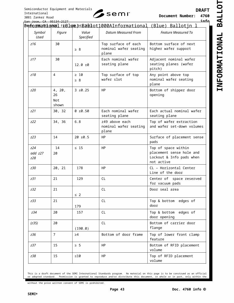
INFO
RM
ATIO
NA
L B
ALL
OT
Informational (Blue) Ballot1000AInformational (Blue) Ballotjn lR1-2 Carrier Options ChecklistTable R1-1 can be used for communicating the compliance of HFOSBs to this standard and the options chosen:Table R1-1
Section Optional Feature Choice
17.1 Rear wafer support yesor
no11.3 info pad A height up (pad missing)
or down (pad present)
11.3 info pad B height up (pad missing)or
down (pad present)11.3 info pad C height up (pad missing)
or down (pad present)
11.3 info pad D height up (pad missing)or
down (pad present)11.3 info pad E height up (pad missing)
or down (pad present)
11.3 info pad F height up (pad missing)or
down (pad present)11.3 Lockout Pad 1 up (pad missing)
or down (pad present)
11.3 Lockout Pad 2 up (pad missing)or
down (pad present)
This is a draft document of the SEMI International Standards program. No material on this page is to be construed as an official or adopted standard. Permission is granted to reproduce and/or distribute this document, in whole or in part, only within the scope of SEMI International Standards committee (document development) activity. All other reproduction and/or distribution without the prior written consent of SEMI is prohibited.
Page 44 Doc. 4760 info SEMI
Semiconductor Equipment and Materials International3081 Zanker RoadSan Jose, CA 95134-2127Phone:408.943.6900 Fax: 408.943.7943
DRAFTDocument Number: 4760 info
Date: 2009/08/13
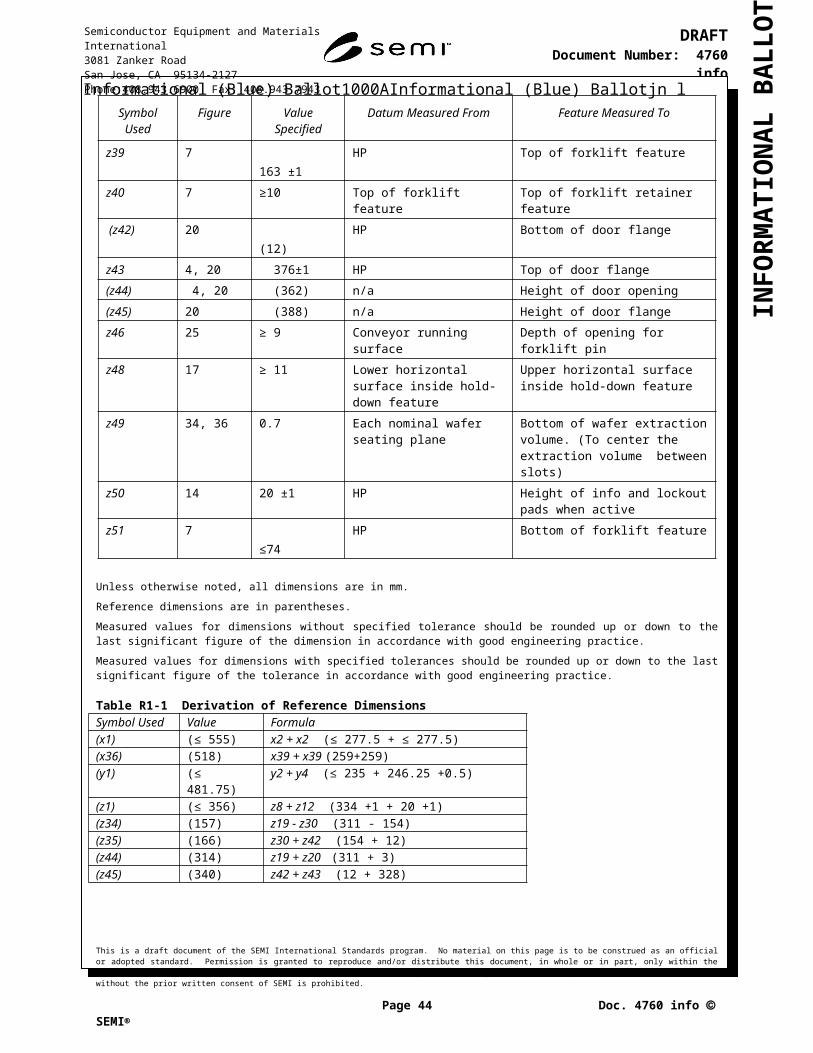
INFO
RM
ATIO
NA
L B
ALL
OT
Informational (Blue) Ballot1000AInformational (Blue) Ballotjn lRELATED INFORMATION 2 CONSIDERATIONS for DETERMINING DIMENSIONS NOTICE: This related information is not an official part of SEMI (doc#) and was derived from the work of the International Physical Interfaces & Carriers Committee. This related information was approved for publication on (date of approval) by the International Physical Interfaces & Carriers Committee.
R2-1 Referenced Standards and DocumentsR2-1.1 Semi StandardsSEMI M74 — Specification for 450 mm Diameter Mechanical Handling Polished Wafers
R2-2 Discussion R2-2.1 The PIC committee considered the specifications in SEMI M74, the draft for the SEMI standard for 450 mm load ports, and this document to determine how much space between wafers and wafer supports is needed for safe handling of wafers. In addition, the following issues were considered: R2-2.1.1 wafer deflection under gravity — the deflection caused by gravity of a wafer resting on the carrier supports directly above the end effector pick-up points and at a 30 degree angle from the line of end effector stroke. Once the wafer has been lifted by the end effector, the deflection will be determined by the design of the end effector and is not considered to add to the budget for the end effector with wafer. The reason for measuring at 30 degrees is that the height of the end effector pads allows for some droop between the pads without the wafer touching the end effector structure. Based on the measurements made by ISMI and simulations done by task force participants, the committee has used the value of 0.50 mm. R2-2.1.2 process induced warp — 300 mm wafers have had process induced warp as great as 1 mm. When this is extrapolated to 450 mm wafer size, the warp would be 1.6mm. With 300 mm wafers, the warp has produced wafers with a convex top surface and a concave top surface. When an end effector is inserted between two wafers the clearance is reduced by 3.2 mm. Once a wafer has been picked up, the effect on clearance will be 1.6 mm since the end effector has moved up away from the wafer below. R2-2.1.3 carrier placement error — the maximum misalignment of the carrier that is expected, based on prototype testing, is 0.2 mm. This error results in the carrier not fully seating on the KC pins, so it is always a positive error. R2-2.2 After testing and discussion the committee has settled on a wafer pitch of 12 mm.
R2-3 Height of wafer extraction and set-down volumes R2-3.1 The height of extraction and set-down volumes dimensions is equal to the clearance between wafer supports minus to tolerance of the wafer planes and the carrier placement error. Since the carrier placement error serves to raise the wafer supports above their nominal position, it causes the volumes to be offset.. So the volumes start 0.7 mm above nominal wafer seating plane and extend to within 0.5 mm of the next wafer support.
R2-4 Kinematic Coupling SystemR2-4.1 The central approach in scaling the kinematic coupling concept to the 450 HFOSB was to try to make the current 300 mm style of pin the plan if possible. While mass of fully loaded 300 mm carriers was 7.6 kg, the mass of 450 mm carriers is estimated to be 24 kg. The increased weight load of the 450 HFOSB meant that the existing 300 mm pin would have provided a contact pressure that could have exceeded safe deformation limits for the likely carrier materials. R2-4.2 The key structure of the 450 HFOSB bottom consists of a pedestal extending below the lowest HFOSB door surface. A number of advantages can be obtained from this approach: More vertical space can be used to increase the “lead-in” or capture area during handoff (more discussion of this
in the detailed discussion of the groove below). Provides separate heights for the conveying surfaces and the door features, so that both features can be better
optimized for their intended purposes. Conveyor rail can be moved inward from the edge, so that the conveying surface does not define the lateral
envelope of the carrier (as both the conveyor rails and the forklift structures did in the 300 mm HFOSB).
This is a draft document of the SEMI International Standards program. No material on this page is to be construed as an official or adopted standard. Permission is granted to reproduce and/or distribute this document, in whole or in part, only within the scope of SEMI International Standards committee (document development) activity. All other reproduction and/or distribution without the prior written consent of SEMI is prohibited.
Page 45 Doc. 4760 info SEMI
Semiconductor Equipment and Materials International3081 Zanker RoadSan Jose, CA 95134-2127Phone:408.943.6900 Fax: 408.943.7943
DRAFTDocument Number: 4760 info
Date: 2009/08/13

INFO
RM
ATIO
NA
L B
ALL
OT
Informational (Blue) Ballot1000AInformational (Blue) Ballotjn l The pedestal base (interior of the conveyor rails) can be made slightly lower (farther from HP) than the
conveying surfaces, providing areas separate from transport structures that can be defined (in later ballots) for sensing features (presence, placement, lockout, info pad, etc.).
Adding these features below the plane of the kinematic coupling pins allows these advantages to be made without requiring additional height between the top of the kinematic coupling pins and the plane of the first (bottom-most) wafer. This is important because it is that dimension which defines the height of the wafer planes above the floor.
R2-4.3 The kinematic coupling pins themselves are similar in shape to those at 300 mm, but are scaled up to control the deformation created by the contact pressure between them and the carrier groove materials. Several different geometries were considered, geometry “B” was selected and is shown below, along with the geometry used for 300 mm systems. R2-4.4 In all cases the materials analyzed were stainless steel for the KCPs and plastic for the grooves.
Table R2-1 Contact Stress at Kinematic Coupling Pins
Design 300 mm (Shape A) 450 mm (Shape B)
Description Current 300 mm KCP 20 mm pin with offset radius 4 mm transition
Pin Diameter (mm) 12 20
Radius Minor (mm) 7.127 11.585
Radius Major (mm) 15 30
Math. Equiv. 5 8
Applied angle 45 degrees 45 degrees
Carrier Mass (kg) 7.6 24
Force (Newtons) 74.53 235.54
Force per pin 24.84 78.52
Stress Ratio 0.92 0.92
Relative contact stress 53,071,124 53,783,837
Result Used for 300 mm 1.34% higher stress
Figure R2-2 Shapes from Table R2-2
R2-4.5 The goal is that even for the most heavily loaded 450 HFOSB, the relative contact stress should not exceed that for 300 mm. To that end, the contact radius is increased from 15 mm to 30 mm and the pin diameter is increased from 12 mm to 20 mm. The resulting wear on the grooves mating to the 450 mm kinematic coupling pins should thus be no worse than that of their 300 mm counterparts. R2-4.6 One common issue for 300 mm FOUP was the occasional problem with the kinematic coupling caused by improper lead-in or “stickiness” that prevented the pin from seating properly. The lead-in issue caused issues with AMHS handoffs, and caused a need for additional axes of motion to rotate the FOUP around a vertical axis to ensure proper capture by the pins for an arbitrarily placed tool and load port. The stickiness issue causes improper seating and can cause bad wafer handling.R2-4.7 To help address both of these issues, the approach in the 450 mm standard has been to define key aspects of the groove surface of the carrier which mates with the kinematic coupling pins. Doing so allows an increased height for improved range of lead-in, and specifying the groove angle at 45 ±6 degrees (θ1) allows for a good balance (trade-off) between capture range and increased HFOSB height. This results in a taller KCP height for the load port
This is a draft document of the SEMI International Standards program. No material on this page is to be construed as an official or adopted standard. Permission is granted to reproduce and/or distribute this document, in whole or in part, only within the scope of SEMI International Standards committee (document development) activity. All other reproduction and/or distribution without the prior written consent of SEMI is prohibited.
Page 46 Doc. 4760 info SEMI
Semiconductor Equipment and Materials International3081 Zanker RoadSan Jose, CA 95134-2127Phone:408.943.6900 Fax: 408.943.7943
DRAFTDocument Number: 4760 info
Date: 2009/08/13

INFO
RM
ATIO
NA
L B
ALL
OT
Informational (Blue) Ballot1000AInformational (Blue) Ballotjn lor shelf. Conversely, the distance can be thought of as specifying an upper plane of an exclusion volume from which load port or shelf features (unrelated to sensing) shall not enter. Increased “capture” or “lead-in” of up to 15 mm (r15) in all directions when the HFOSB is oriented properly in
angle Rotations of the HFOSB around its z axis of a few degrees can still allow enough capture range so that 450 mm
AMHS vehicles and systems may be able to have better speed and reliability for the factories.R2-4.8 To describe the capture, consider figure R2-2:
Figure R2-1 Kinematic Coupling Pin and Groove Detail
R2-4.9 Figure R2-2 shows how the specification ensures that even a 15 mm offset can be captured. Note that because of the shape of the pin and the fact that the contact point is at the 45-degree plane, not at the tip of the point, so that the opening of the groove is larger than 15 mm to guarantee a 15 mm offset can be corrected.R2-4.10 An angular misalignment of the HFOSB during handoff is also possible. Ensuring a 15 mm lead-in for the case which is properly aligned angularly will allow a greater tolerance for angular misalignment than in the 300 mm case. R2-4.11 Another issue at 300 mm was the fact that the wafer center was not the center of mass of the carrier. Thus AMHS or other systems that handled the HFOSB had to deal with gravitational torques that changed in magnitude depending on the number of wafers in the carrier. This limited transfer speeds and added complexity to handling.R2-4.12 At 450 mm, the approach has been to align the center of mass of the carrier with the center of the automation flange, and allow this to be forward of the FP and the center of the wafers. Doing so has the advantage
This is a draft document of the SEMI International Standards program. No material on this page is to be construed as an official or adopted standard. Permission is granted to reproduce and/or distribute this document, in whole or in part, only within the scope of SEMI International Standards committee (document development) activity. All other reproduction and/or distribution without the prior written consent of SEMI is prohibited.
Page 47 Doc. 4760 info SEMI
Semiconductor Equipment and Materials International3081 Zanker RoadSan Jose, CA 95134-2127Phone:408.943.6900 Fax: 408.943.7943
DRAFTDocument Number: 4760 info
Date: 2009/08/13
INFO
RM
ATIO
NA
L B
ALL
OT
Informational (Blue) Ballot1000AInformational (Blue) Ballotjn lnot only of simpler HFOSB handling (the critical handling feature will all be weight-balanced for any number of wafers in the HFOSB), but also eliminates the need for a counterweight. To compensate for the change in center of gravity, the front kinematic coupling pins were moved forward to keep the loads on the pins approximately equal.
The location of the kinematic coupling pins was designed to allow a forklift to pass under the carrier from the front and from the side to transfer the carrier from primary to secondary pins.
R2-4.13 In keeping with the philosophy of explicitly designating guiding and sensing surfaces in the 450mm standards, the outside edges of the conveyor rails is called to be vertical surface at x5 and y5 with material (for guiding surface) extending at least 9mm up. No blend radius has yet been defined for the junction of the conveying surface and the vertical guiding surface, but that corner is meant to be relatively sharp (blend radius is suggested to be less than 0.5mm). To provide a volume for the conveyor edge rails and any corresponding sensing mechanics, the volume external to x5 and y5 from the BP and FP is defined as clear of HFOSB features up to the height of at least 8mm. This is true not only for “pedestal” features but also for the bottom surface of any door flange of the shell.R2-4.14 The conveyor rails have been defined as having a square footprint centered at the origin. This will allow conveyance of the HFOSB in any of the four orientations on the same conveyor unit, enabling possible new handling and loading approaches in the factory. Having the rails the same length and centered close to the carrier center of mass will avoid handling issues such as twisting or undulating, and should improve vibration performance during transport and handling.
R2-5 Forces on the Carrier DoorR2-5.1 The values in the following table are based on estimates provided by several parties. The highest values submitted were placed in the table.Table R2-1 Carrier Door Forces
Door Seal Gasket ForcesDoor Seal Height (mm) 358 Blue BallotDoor Seal Width (mm) 514 Blue BallotDoor Seal Perimeter (mm) 1744 CalculatedDoor Seal Force/Length (N/mm) 0.06 Door Seal Total Force (N) 105
Shell Seal Gasket ForcesShell Seal Height (mm) 342 Blue BallotShell Seal Width (mm) 560 Blue BallotShell Seal Perimeter (mm) 1804 Calculated
Shell Seal Force/Length (N/mm) 0.025Should be determined by load port companies.
Shell Seal Total Force (N) 45.1
Wafer Retention ForcesShock Load Wafer Retention Capability Without Cross Slotting and Assurance That Wafers Will Be In Pick-Up Volume After Transport From Point A to Point B (G)
1
Wafer Retention Force 25 Wafers (N) 122 Transport Shock ‘Wafer Mass’ (N) 938
This is a draft document of the SEMI International Standards program. No material on this page is to be construed as an official or adopted standard. Permission is granted to reproduce and/or distribute this document, in whole or in part, only within the scope of SEMI International Standards committee (document development) activity. All other reproduction and/or distribution without the prior written consent of SEMI is prohibited.
Page 48 Doc. 4760 info SEMI
Semiconductor Equipment and Materials International3081 Zanker RoadSan Jose, CA 95134-2127Phone:408.943.6900 Fax: 408.943.7943
DRAFTDocument Number: 4760 info
Date: 2009/08/13
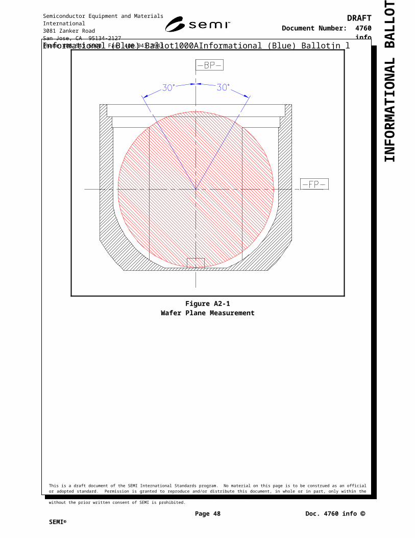
INFO
RM
ATIO
NA
L B
ALL
OT
Informational (Blue) Ballot1000AInformational (Blue) Ballotjn l
Not
App
licab
le
Dur
ing
Ope
n/C
lose
R2-5.2 The Wafer Retention force and Door Seal Gasket force must be applied in order to close the carrier door. So the door closing force is 105 N plus 122 N or 227 N. The Internal Pressure and Shell Seal Gasket forces not apply to door closing.
This is a draft document of the SEMI International Standards program. No material on this page is to be construed as an official or adopted standard. Permission is granted to reproduce and/or distribute this document, in whole or in part, only within the scope of SEMI International Standards committee (document development) activity. All other reproduction and/or distribution without the prior written consent of SEMI is prohibited.
Page 49 Doc. 4760 info SEMI
Semiconductor Equipment and Materials International3081 Zanker RoadSan Jose, CA 95134-2127Phone:408.943.6900 Fax: 408.943.7943
DRAFTDocument Number: 4760 info
Date: 2009/08/13

INFO
RM
ATIO
NA
L B
ALL
OT
Informational (Blue) Ballot1000AInformational (Blue) Ballotjn lRELATED INFORMATION 3 CARRIER HOLD-DOWN FEATURENOTICE: This related information is not an official part of SEMI (doc#) and was derived from the work of the International Physical Interfaces & Carriers Committee. This related information was approved for publication on (date of approval) by the International Physical Interfaces & Carriers Committee.
R3-1 The hold-down features on the bottom of the 450 HFOSB are meant to interact with their counterparts on the load port and AMHS systems to provide multiple uses for hold-down and support, namely: On load ports, Force for frame-to-shell seal On load ports, Force to counter door-closing force during that action On load ports and shelves, force to impede unauthorized removal On AMHS transfer devices (robots, AGV, OHS, etc.), forces to avoid loss of HFOSB during rapid
acceleration/deceleration/EMOR3-1.1 Load Port Hold-Down Interactions. The load port is the primary user of the hold-down feature. In this Related Information, the Standards team felt it was important for prospective users of the standard to understand what the hold-down function WAS and WAS NOT. The hold-down is NOT intended to be a work-around for an otherwise non-functional kinematic coupling; that is, in the presence of only gravity, the carrier is always expected to slide down to the proper seated position without the need for other external forces. For example, following a small “upset” force (human push, cart bumping the load port, etc.) the 450 HFOSB should return to its proper seating on the pins without the need for external forces beyond gravity. This statement is also expected to be true for the case where the carrier is docked with its door OPEN and the (optional?) seal between the load port frame and carrier shell is maintained; any “maintenance” downward force exerted by the load-port hold-down device onto the carrier hold-down feature is expected to be small (actual values are not yet defined, but expected to no more than 20N to 40N, or well under 10% of the loaded carrier weight). This force is meant to be kept relatively small so that neither the carrier shell nor the wafer support plane is altered by the hold-down.R3-1.2 During door opening (and especially door closing) there may be substantial forces being applied to the HFOSB shell. At 300mm, these were 9N for FOUP and up to 110N for FOSBs. At 450mm the values are still not set, and may depend on the type of seal needed to hold environment inside the carrier, In fact, given some minimum “lead-in” for the 450 HFOSB door into its shell, some slight horizontal motion may occur during the door closing process. Multiple designs could accomplish this, such as the various physical analogs of the force profile of one light spring (for the constant force) in parallel with a heavy spring with a non-elastic slack (so that a large force can be applied but only after some small motion). The direction of the resultant force would be downward and toward the door, to act against the tendency of the door-closing operation to push the front Kinematic Coupling Grooves up off their seated position on the pins.R3-1.3 The final Load-Port hold-down functionality is to prevent unauthorized removal of the carrier during use. While automated systems should be able to avoid this through the (to-be-developed) next generation handoff protocol, there is still an opportunity for carriers to be removed in a “semi-automated” fashion (using a mechanically assisted lifting cart, for example). If these semi-automatic lifters had a force-actuated switch, it could trigger an alarm when attempting to operate against a hold-down. This functionality would imply that the switch force would have to be set at a force significantly above the maximum weight of a loaded 450 HFOSB (say 130%?). Conversely, this sets a minimum “tear away” force on the hold-down feature on the carrier, which should be the maximum “alarm” force times a safety factor. One possible value would be 200% of the maximum carrier weight. This value is consistent with the “emergency stop” function described in the next paragraph
R3-2 AMHS Hold-Down Interactions. AMHS systems (such as RGV, AGV, stocker crane end effectors, or other robotic lifters) may need to hold the 450 HFOSB by the secondary kinematic coupling pins. The Hold-down features are also designed to be used by the AMHS system to help prevent unwanted tipping or sliding of the carrier, perhaps during a robotic EMO event. The forces from these events may be in different directions, depending upon the direction of robotic motion at the time of the EMO. In the worst case of the fastest robot, this deceleration could be on the order of several “g” so that the holder would need to maintain multiple carrier weights (if it is to be the only feature used for retention during such an event).
This is a draft document of the SEMI International Standards program. No material on this page is to be construed as an official or adopted standard. Permission is granted to reproduce and/or distribute this document, in whole or in part, only within the scope of SEMI International Standards committee (document development) activity. All other reproduction and/or distribution without the prior written consent of SEMI is prohibited.
Page 50 Doc. 4760 info SEMI
Semiconductor Equipment and Materials International3081 Zanker RoadSan Jose, CA 95134-2127Phone:408.943.6900 Fax: 408.943.7943
DRAFTDocument Number: 4760 info
Date: 2009/08/13

INFO
RM
ATIO
NA
L B
ALL
OT
Informational (Blue) Ballot1000AInformational (Blue) Ballotjn lR3-2.1 Hold-Down Feature Shape to Support Different Hold-Down Elements. The shape and size of the 450 HFOSB hold-down feature is designed to allow differing access methods for differing applications, in keeping with the 450mm standards philosophy of using fewer features to do multiple functions to simply the standards and implementation. The front (door-side) feature, with its 30-degree slope and shelf, will support a “hook” style retainer facing toward the carrier door, in a way that supports downward and forward forces to be applied by the hooks. The “mirroring” of this feature to the rear would allow access by “V”-shaped keys which rotate about their vertical access, or for “T” shape keys, similar in shape to the E62 keys (but with different forces and motions, of course). The point of this related information of the standard is not to pick a design, but to allow multiple innovations to address the problem but understand the basic multiple requirements.
This is a draft document of the SEMI International Standards program. No material on this page is to be construed as an official or adopted standard. Permission is granted to reproduce and/or distribute this document, in whole or in part, only within the scope of SEMI International Standards committee (document development) activity. All other reproduction and/or distribution without the prior written consent of SEMI is prohibited.
Page 51 Doc. 4760 info SEMI
Semiconductor Equipment and Materials International3081 Zanker RoadSan Jose, CA 95134-2127Phone:408.943.6900 Fax: 408.943.7943
DRAFTDocument Number: 4760 info
Date: 2009/08/13
INFO
RM
ATIO
NA
L B
ALL
OT
Informational (Blue) Ballot1000AInformational (Blue) Ballotjn lRELATED INFORMATION 4 CARRIER PRESENCE AND PLACEMENT AREASNOTICE: This related information is not an official part of SEMI (doc#) and was derived from the work of the International Physical Interfaces & Carriers Committee. This related information was approved for publication on (date of approval) by the International Physical Interfaces & Carriers Committee.
R4-1 One of the key “Lessons Learned” from the 300mm standards was that considerable problems were created by leaving sensing areas undefined in location and purpose, as load port and AMHS makers used locations and methods that did not always have a corresponding feature on the carrier side.R4-1.1 This 450mm standard, defines specific locations and characteristics for sensing and information. One example of these is the presence and placement sensing areas on the carrier bottom.R4-1.2 The purpose of Presence sensing is to alert the manipulating device (load port, robot, AMHS device) that a carrier (or something) is present, but may or may not be correctly placed and loaded yet for processing or handoff.R4-1.3 In the case of a load port, the presence sensing is primarily to ensure that automated deliveries do not occur to an occupied location, even if the carrier occupying that location is misplaced. It must therefore still be functional even if the carrier were, say, sitting atop the pins but not seated in the grooves. Even though carriers will not be “hand-delivered” at 450mm, they may be “semi-automatically” delivered (using human-steered lifting assistance). Thus the load port still needs to be able to detect when a 450 HFOSB is misplaced. The approach taken in the 450mm standard is to define a flat, opaque (at least to red and infrared, the most common LED sensor wavelengths) spot about the center of the wafer. R4-1.4 Typical tests used are to move the carrier:R4-1.4.1 Leftward or rightward a fixed distance from seated, and still be detectable. The area centered on the FP and BP allows a full 19 cm in either direction to be detected. An alternate proposal that limits the band to 5 cm either side of the BP would allow motion of 5 cm either left or right to be detected (more if sensors were angled).R4-1.4.2 Forward a fixed distance. The band proposed in this ballot would extend 30mm from the FP, so that a sensor at the HFOSB center could see a 3 cm forward movement and still be detectable (note under the current likely load port proposal the carrier would then be touching the load port door already).R4-1.4.3 Backward a fixed distance. Again, the band would ensure detection up to a motion of 3 cm away from the door. Misplacement farther than that would require a larger dark spot / bottom plate, or an opaque substrate in or near the bottom slot of the carrier.R4-1.4.4 Rotations about the carrier center (of a few degrees, or a right angle, or reversed). The band at the carrier center (and the corresponding sensor likewise on the load port) will allow the carrier to be detected with arbitrary angular orientation (although it should be noticed that on a load port only a few degrees of misalignment would be possible before the carrier would interfere with the load port door or the carrier on the adjacent load port.
R4-2 Placement sensing false positive R4-2.1 A carrier placement false positive may occur due to offset placement of a carrier on the load port if the KC pins slip into open cavities in the carrier bottom.
NOTICE: SEMI makes no warranties or representations as to the suitability of the standards set forth herein for any particular application. The determination of the suitability of the standard is solely the responsibility of the user. Users are cautioned to refer to manufacturer's instructions, product labels, product data sheets, and other relevant literature, respecting any materials or equipment mentioned herein. These standards are subject to change without notice.
The user’s attention is called to the possibility that compliance with this standard may require use of copyrighted material or of an invention covered by patent rights. Entegris, Inc. has filed a statement with SEMI asserting that licenses will be made available to applicants throughout the world for the purpose of implementing this standard without unfair discrimination. Attention is also drawn to the possibility that some elements of this standard may be subject to patented technology or copyrighted items other than those identified above. Semiconductor Equipment and Materials International (SEMI) shall not be held responsible for identifying any or all such patented technology
This is a draft document of the SEMI International Standards program. No material on this page is to be construed as an official or adopted standard. Permission is granted to reproduce and/or distribute this document, in whole or in part, only within the scope of SEMI International Standards committee (document development) activity. All other reproduction and/or distribution without the prior written consent of SEMI is prohibited.
Page 52 Doc. 4760 info SEMI
Semiconductor Equipment and Materials International3081 Zanker RoadSan Jose, CA 95134-2127Phone:408.943.6900 Fax: 408.943.7943
DRAFTDocument Number: 4760 info
Date: 2009/08/13

INFO
RM
ATIO
NA
L B
ALL
OT
Informational (Blue) Ballot1000AInformational (Blue) Ballotjn lor copyrighted items. By publication of this standard, SEMI takes no position respecting the validity of any patent rights or copyrights asserted in connection with any item mentioned in this standard. Users of this standard are expressly advised that determination of any such patent rights or copyrights and the risk of infringement of such rights are entirely their own responsibility.
This is a draft document of the SEMI International Standards program. No material on this page is to be construed as an official or adopted standard. Permission is granted to reproduce and/or distribute this document, in whole or in part, only within the scope of SEMI International Standards committee (document development) activity. All other reproduction and/or distribution without the prior written consent of SEMI is prohibited.
Page 53 Doc. 4760 info SEMI
Semiconductor Equipment and Materials International3081 Zanker RoadSan Jose, CA 95134-2127Phone:408.943.6900 Fax: 408.943.7943
DRAFTDocument Number: 4760 info
Date: 2009/08/13

INFO
RM
ATIO
NA
L B
ALL
OT
Informational (Blue) Ballot1000AInformational (Blue) Ballotjn lDraft Document 4760
NEW STANDARD: MECHANICAL SPECIFICATION FOR FRONT-OPENING SHIPPING BOX USED TO TRANSPORT AND SHIP 450mm WAFERS – Design B 1 Purpose1.1 This standard specifies the front-opening shipping box (FOSB) used to ship 450 mm wafers from wafer suppliers to their customers (typically IC manufacturers), while maintaining wafer quality.
2 Scope 2.1 This standard is intended to set an appropriate level of specification that places minimal limits on innovation while ensuring modularity and interchangeability at all mechanical interfaces. However, this standard has been written so that injection-molded plastic FOSBs can be manufactured in conformance with it, and those can be utilized for maintaining wafers quality during transportation, opening and closing the door.
2.2 This standard assumes that the FOSB is used in loading raw silicon wafers to FOSB after inspection in Si suppliers and also used in acceptance and inspection and transfer to another carrier at device makers. The FOSB is not intended to be used in IC manufacturing processes. It is recommended that wafers be transferred from the FOSB to a FOUP using automated methods.
NOTICE: This standard does not purport to address safety issues, if any, associated with its use. It is the responsibility of the users of this standard to establish appropriate safety and health practices and determine the applicability of regulatory or other limitations prior to use.
3 Limitations3.1 This standard is to allow prototyping data gathering in 2H’09, and is to be revised based on the prototyping and gathered data for yellow ballot.
4 Referenced Documents and Standards4.1 SEMI Standards
SEMI M74 ― Specification for 450 mm Diameter Mechanical Handling Polished Wafers
SEMI Draft Document 4624 - Specification for Developmental 450 mm Diameter Polished Single Crystal Silicon Wafers
SEMI Draft Document 4570B— Mechanical Specification for FOUPS Used to Transport and Store 450 mm Wafers
SEMI Draft Document 4599B — Mechanical Interface Specification for 450 mm Load Port
SEMI XXX— Standard for 450mm Wafer Shipping System
SEMI AUX16— List of carrier maker Identification Codes
4.2 ISO Standards2
ISO/IEC 16022 — International Symbology Specification - Data Matrix
NOTICE: Unless otherwise indicated, all documents cited shall be the latest published versions.
5 Terminology5.1 Abbreviations and Acronyms
5.1.1 2D – two dimensional
2 International Organization for Standardization (ISO), ISO Central Secretariat, 1, ch.de la Voie-Creuse, Case postale 56, CH-1211 Geneva 20, Switzerland. Telephone: 41.22.749.01.11; Fax: 41.22.733.34.30; http://www.iso.ch
This is a draft document of the SEMI International Standards program. No material on this page is to be construed as an official or adopted standard. Permission is granted to reproduce and/or distribute this document, in whole or in part, only within the scope of SEMI International Standards committee (document development) activity. All other reproduction and/or distribution without the prior written consent of SEMI is prohibited.
Page 54 Doc. 4760 info SEMI
Semiconductor Equipment and Materials International3081 Zanker RoadSan Jose, CA 95134-2127Phone:408.943.6900 Fax: 408.943.7943
DRAFTDocument Number: 4760 info
Date: 2009/08/13

INFO
RM
ATIO
NA
L B
ALL
OT
Informational (Blue) Ballot1000AInformational (Blue) Ballotjn l5.1.2 BP — bilateral plane
5.1.3 CL — center line
5.1.4 EE — end effector
5.1.5 FOSB —front-opening shipping box
5.1.6 FP — facial plane
5.1.7 HP — horizontal plane
5.1.8 KC ― kinematic coupling
5.1.9 KCP — kinematic coupling pin
5.1.10 OHT ― overhead hoist transport
5.1.11 RFID ― radio frequency identification
5.1.12 TIR — total indicator runout
5.2 Definitions
5.2.1 2D code — a code identifying elements such as maker, model, version and serial number of a FOSB, by using Data Matrix ECC200 symbol according to ISO/IEC 16022.
5.2.2 2D code placement area — an area on the door and another area on top of the shell, where a 2D code can be placed.
5.2.3 450 FOSB — a front opening shipping box with a front-opening interface, used to ship 450 mm wafers from wafer suppliers to their customers (typically IC manufacturers), while maintaining wafer quality.
5.2.4 bilateral plane (BP) — a vertical plane, defining x=0 of a system with three orthogonal planes, the plane passes through the location of the rear kinematic pin on the load port, and midway between the front kinematic pin locations on the load port.
5.2.5 carrier — an open structure that holds one or more substrates.
5.2.6 center line (CL) — a horizontal line centered vertically on the carrier door used as the reference for z dimensions of door features.
5.2.7 end effector — an end effector designed to support wafers for transferring wafers from the carrier’s wafer supports.
5.2.8 facial plane (FP) — a vertical plane, defining y=0 of a system with three orthogonal planes, perpendicular to the BP and located 194 mm in front of the rear kinematic pin.
5.2.9 front (of shipping box) — the part of the shipping box closest to the door.
5.2.10 horizontal plane (HP) — a horizontal plane, defining z=0 of a system with three orthogonal planes, coincident with the uppermost points (tips) of the three kinematic coupling pins.
5.2.11 origin — the intersection of the BP and FP.
5.2.12 plane ― a theoretical surface which has infinite width and length, zero thickness and zero curvature.
5.2.13 rear (of shipping box) — the part of the shipping box farthest from its door.
5.2.14 wafer deflection — change in wafer shape (TIR) due to gravity while the wafer is resting on the shipping box wafer supports with the shipping box door open.
5.2.15 wafer seating plane — the bottom surface of an ideally rigid flat disk that meets the diameter specification for 450 mm wafers, with negligible droop due to gravity, as it rests on the wafer supports.
5.2.16 shipping box capacity — the number of substrates that a shipping box holds.
5.2.17 shipping box sensing pads — surfaces on the bottom of the shipping box for triggering optical or mechanical sensors.
This is a draft document of the SEMI International Standards program. No material on this page is to be construed as an official or adopted standard. Permission is granted to reproduce and/or distribute this document, in whole or in part, only within the scope of SEMI International Standards committee (document development) activity. All other reproduction and/or distribution without the prior written consent of SEMI is prohibited.
Page 55 Doc. 4760 info SEMI
Semiconductor Equipment and Materials International3081 Zanker RoadSan Jose, CA 95134-2127Phone:408.943.6900 Fax: 408.943.7943
DRAFTDocument Number: 4760 info
Date: 2009/08/13

INFO
RM
ATIO
NA
L B
ALL
OT
Informational (Blue) Ballot1000AInformational (Blue) Ballotjn l5.2.18 front-opening unified pod (FOUP) — a box (that complies with SEMI Doc. 4570B) with a non-removable cassette (so that its interior complies with SEMI Doc. 4570B) and with a front-opening interface (that mates with a FIMS port that complies with SEMI Doc. 4599B).
5.2.19 minienvironment — a localized environment created by an enclosure to isolate the product from contamination and people.
5.2.20 shipping box — a protective portable container for a carrier and/or wafer(s) that is used to ship wafers from the wafer suppliers to their customers.
5.2.21 wafer extraction volume — the open space for extracting a wafer from the shipping box.
5.2.22 wafer pick-up volume — the space that contains entire bottom of a wafer if the wafer has been pushed to the rear of the shipping box.
5.2.23 wafer set-down volume — the open space for inserting and setting down a wafer in the shipping box.
6 Reference Planes (HP, FP, BP) Specification6.1 The HP, FP, and BP as described in the definition section are ideal planes, which are intended to be used to depict the position of certain features relatively to these planes. These planes are at position zero (x, y, z) with no tolerance associated, since these ideal planes do not represent a physical feature.
FP and BP are defined as vertical planes and ideally are parallel to the gradient of the gravity field. All three planes are mutually perpendicular. Only positive numbers are used to define coordinates within this system of three planes. No negative numbers are used in order to be as close as possible to standard mechanical drawing practices. Necessary clarification on the position of a feature usually will be achieved via figures.
6.2 Reference Baselines — One centerlines is defined:
CL — Centerline for the carrier door. It passes through the centers of the openings for the door pins. All the z-dimensions of door features are symmetric to the CL.
7 Shipping Box Envelope 7.1 The overall dimensions of the 450 FOSB, (x1), (y1), and (z1), are given as reference dimensions because they are derived from other dimensions. See Table 2. Overviews of 450 FOSB are shown in Figure 1.
(x1) ≤ x2*2
(y1) ≤ y2 + y4max
(z1) ≤ x8max + z11
This is a draft document of the SEMI International Standards program. No material on this page is to be construed as an official or adopted standard. Permission is granted to reproduce and/or distribute this document, in whole or in part, only within the scope of SEMI International Standards committee (document development) activity. All other reproduction and/or distribution without the prior written consent of SEMI is prohibited.
Page 56 Doc. 4760 info SEMI
Semiconductor Equipment and Materials International3081 Zanker RoadSan Jose, CA 95134-2127Phone:408.943.6900 Fax: 408.943.7943
DRAFTDocument Number: 4760 info
Date: 2009/08/13

INFO
RM
ATIO
NA
L B
ALL
OT
Informational (Blue) Ballot1000AInformational (Blue) Ballotjn l
Figure1 Overall Views of 450 FOSB
8 Requirements8.1 The FOSB has the following components and sub-components:
Key:
Required feature
Optional feature
Rear RFID Tag Placement Volume
Door on front Automated door 2D code placement area Holes for latch keys that lock the door to the FIMS interface when the door is unlatched from the box
This is a draft document of the SEMI International Standards program. No material on this page is to be construed as an official or adopted standard. Permission is granted to reproduce and/or distribute this document, in whole or in part, only within the scope of SEMI International Standards committee (document development) activity. All other reproduction and/or distribution without the prior written consent of SEMI is prohibited.
Page 57 Doc. 4760 info SEMI
Semiconductor Equipment and Materials International3081 Zanker RoadSan Jose, CA 95134-2127Phone:408.943.6900 Fax: 408.943.7943
DRAFTDocument Number: 4760 info
Date: 2009/08/13

INFO
RM
ATIO
NA
L B
ALL
OT
Informational (Blue) Ballot1000AInformational (Blue) Ballotjn l Holes for door pins Door presence sensing areas Reserved area for vacuum pads
Top
Automation flange
2D code placement area
Front clamp feature
Interior
Cassette with supports for 25 wafers
Wafer retainer
End effector exclusion zone
Sides
Folk lift feature
Bottom
7 carrier sensing pads
6 Info pads
2 Lockout pin holes
3 features that mate with kinematic coupling pins and provide a 15 mm lead-in
Bottom clamp feature
Front clamp feature
8.2 Kinematic Couplings — The physical alignment mechanism from the FOSB to the tool load-port (or a nest on a vehicle or in a stocker) consists of features (not specified in this standard) on the top entity that mate with six pins underneath as defined in SEMI Doc.4570B. The three features that mate with the kinematic coupling pins must provide a lead-in capability that corrects a FOSB misalignment of up to r42 in any horizontal direction.
8.3 Inner and Outer Radii — All required concave features may have a radius of up to r40 to allow cleaning and to prevent contaminant build-up. All required convex features may also have a radius of up to r41 to prevent small contact patches with large stresses that might cause wear and particles. Note that these limits on the radius of all required features are specified as a maximum (not a minimum) to ensure that the required features are not rounded off too much. The lower bound on the radius is up to the FOSB supplier. Note also that this radius applies to every required feature unless another radius is called out specifically. Here a required feature is an area on the surface of the FOSB supplier. Note also that this radius applies to every required feature unless another radius is called out specifically. Here a required feature is an area on the surface of the FOSB specified by a dimension (or intersections of dimensions) that has a tolerance and not just a maximum or minimum (such as the edges of the robotic handling flange).
8.4 Door — It is recommended that the FOSB not be vertical when it is opened or closed. When the FOSB is in a vertical orientation with the door removed, the wafers must be restrained from touching each other by appropriate wafer support design or other retaining techniques. See Figure 2-4.
8.4.1 Door features – Door has features such as Door Seal Area, Frame Seal Area, Latch Key Opening, Door Pin Opening, Door Sense Area and Area for Vacuum Pads. See figure 2.
8.4.2 The features and sizes of latch keys and door pins of the door must be designed to mate with a port that conforms to SEMI Doc.4599B. However, The location of latch keys and door pins is not the same as 450 FOUP, because of the different door size of FOSB. The location of latch key and door pin are specified in Table 1.
This is a draft document of the SEMI International Standards program. No material on this page is to be construed as an official or adopted standard. Permission is granted to reproduce and/or distribute this document, in whole or in part, only within the scope of SEMI International Standards committee (document development) activity. All other reproduction and/or distribution without the prior written consent of SEMI is prohibited.
Page 58 Doc. 4760 info SEMI
Semiconductor Equipment and Materials International3081 Zanker RoadSan Jose, CA 95134-2127Phone:408.943.6900 Fax: 408.943.7943
DRAFTDocument Number: 4760 info
Date: 2009/08/13

INFO
RM
ATIO
NA
L B
ALL
OT
Informational (Blue) Ballot1000AInformational (Blue) Ballotjn l8.4.3 The spaces for vacuum application are the four circles bounded by r28 and located at x49 & z31. The vacuum pad areas, door seal areas, frame seal areas and door sense areas shall be at a distance of y4 from the FP when the door is closed and latched. No surface on the FOSB door may project further from the FP than these areas and the reserved spaces.
8.4.4 Dimension y39 assures that there is clearance between the door and latch keys when the FOSB is pressed against the FIMS port and both latch keys on the port are inserted to their full length.
8.4.4.1 When the latch keys are turned more than 45° toward the position that unlocks the FOSB door from the FOSB, the latch key holes on the door shall be such that the door is not removable from the latch keys.
8.4.4.2 To allow for unobstructed latch key rotation, the thickness of the outer panel of the carrier door in the area defined by r23 shall be y10. Clearance for latch keys shall be provided by y39 at (x44). Clearance for door pins shall be provided by y40 at (x45). The latchkeys and door pins shall be located on the centerline (CL). See Figure 2.
8.4.4.3 FOSB door features are symmetrical about the CL. Features other than the openings for Frame Pins and Door Pins are symmetrical about the BP.
8.4.5 The opening for the door pin on the left side is circular with diameter (d4), and the opening on the right side is a slot. See Figure 5.
Figure2 450 FOSB Door Features8.4.6 The frame seal area is bounded by x11 & x64 on the sides, by z27 & z34 on the top, and by z28 & z43 on the bottom. There are blend radii r30 and r36 at the inner and outer corners respectively.8.4.7 The door seal area is bounded by x47 on the sides, and by z33 on the top and bottom. The width of the seal area is given by x48 and z32. There are blend radii of r31 & r32 at the outer and inner edges respectively.
8.4.8 Neither the FOSB door opening nor the frame opening is specified. But the door and its position on the load port door shall be controlled so the gap between the load port door and the load port door opening is not obstructed. x47 and z33 are the limits for the door and any variation in its position on the load port door.
This is a draft document of the SEMI International Standards program. No material on this page is to be construed as an official or adopted standard. Permission is granted to reproduce and/or distribute this document, in whole or in part, only within the scope of SEMI International Standards committee (document development) activity. All other reproduction and/or distribution without the prior written consent of SEMI is prohibited.
Page 59 Doc. 4760 info SEMI
Semiconductor Equipment and Materials International3081 Zanker RoadSan Jose, CA 95134-2127Phone:408.943.6900 Fax: 408.943.7943
DRAFTDocument Number: 4760 info
Date: 2009/08/13

INFO
RM
ATIO
NA
L B
ALL
OT
Informational (Blue) Ballot1000AInformational (Blue) Ballotjn l
Figure3 450 FOSB Door Frame
Figure4 450 FOSB Door
This is a draft document of the SEMI International Standards program. No material on this page is to be construed as an official or adopted standard. Permission is granted to reproduce and/or distribute this document, in whole or in part, only within the scope of SEMI International Standards committee (document development) activity. All other reproduction and/or distribution without the prior written consent of SEMI is prohibited.
Page 60 Doc. 4760 info SEMI
Semiconductor Equipment and Materials International3081 Zanker RoadSan Jose, CA 95134-2127Phone:408.943.6900 Fax: 408.943.7943
DRAFTDocument Number: 4760 info
Date: 2009/08/13

INFO
RM
ATIO
NA
L B
ALL
OT
Informational (Blue) Ballot1000AInformational (Blue) Ballotjn l
Figure5 Detail H – Frame Pin and Door Pin Area - Right Side
8.4.9 Wafer Retaining Structure — The slot is usually designed that wafers are suspended in the slot without contacting the surface of the slot for preventing the damage during transportation when FOSB door is closed. It should be noted that wafer position of FOSB is different from that of FOUP when the door is closed due to the wafer retaining structure.
8.4.10 Rear of Door (y60) — FOSB has a y60 100 mm to hold wafers in large area at front wafer retainer for keeping wafer quality during transportation.
8.4.11 Door Closing Force —The force required to push the carrier door into the carrier shell to its fully seated position is f234. The application of f234 to the door shall push the door fully closed, so that the outer surface of the door is equal to y4 from the FP. With the door in this position, the latches shall operate without exceeding the torque limit f230 for the latch keys.
1:Carrier suppliers should design their products to keep this force required to close as small as possible to ensure no damage will occur to wafers upon opening and closing the door.
8.4.12 Latch Torque — The maximum torque required to turn each of the latch mechanisms (with which the latch keys of a load port will engage) on the shipping box door is f230.
8.4.13 Door Latching and Unlatching ― The door of the FOSB must be designed so that the door is completely latched or completely unlatched when the door latch keys are turned to the angular positions described in the relevant SEMI Mechanical Interface Specification for 450 mm Load Ports for FOSB.
8.4.14 A door should be able to withstand a force when applied to one of the retaining features of up to f002 in any direction without negative impact to the intended function of the FOSB (e.g., shell deformation, wafer positions, door closing capabilities).
8.5 Front Clamp Features — The FOSB shall have provision for being clamped at the front of the shipping box.
8.5.1 There shall be two front clamping features on the top of the FOSB. Each is a rectangular depression with a depth of z5, and is bounded by x15 & x16, and by y43 & y44. See Figure 15.
8.5.2 There shall be two front clamping features on the bottom of the FOSB. They shall be rectangular depression with a depth of z36 and be bounded by x15 & x16, and by y43 & y44. See Figure 18.
2: It is recommended that the front clamp features not be used for pulling the FOSB from the undocked position into the FIMS interface. Also, all of the dimensions of the FOSB (such as the wafer location, etc.) are defined with reference to the kinematic coupling pins, and will be in the proper location only when the FOSB is held in place on the kinematic coupling pins only by gravity.
This is a draft document of the SEMI International Standards program. No material on this page is to be construed as an official or adopted standard. Permission is granted to reproduce and/or distribute this document, in whole or in part, only within the scope of SEMI International Standards committee (document development) activity. All other reproduction and/or distribution without the prior written consent of SEMI is prohibited.
Page 61 Doc. 4760 info SEMI
Semiconductor Equipment and Materials International3081 Zanker RoadSan Jose, CA 95134-2127Phone:408.943.6900 Fax: 408.943.7943
DRAFTDocument Number: 4760 info
Date: 2009/08/13

INFO
RM
ATIO
NA
L B
ALL
OT
Informational (Blue) Ballot1000AInformational (Blue) Ballotjn l
NOTE 1:
Figure6 Detail I - Section at Door Centerline - Looking Down on the Right Side8.6 Wafer Retaining — When the FOSB door is closed, the wafers must be retained in the FOSB to prevent movement during subsequent handling, including shipping. It should be noted that wafers are typically shipped in a vertical orientation and generally require support from a secondary package. FOSB and its secondary container should be designed to prevent wafer breakage by accidental drop of the container from a height of 510mm.
8.7 Wafer Orientation and Numbering — The wafers must be horizontal when the FOSB is placed on the coupling, and the wafers slots are numbered in increasing order from bottom to top (so the bottom wafer is wafer number 1, the next wafer up is wafer number 2, etc.).
8.8 Internal Horizontal Dimensions — Figure 7 shows a cross-section of the horizontal boundaries of the FOSB side domains (which contain the parts of the FOSB higher than z25 above the HP and lower than z15 above the top wafer). In this and following figures, the most heavy lines are used for surfaces that have tolerances (not surfaces that have only maximum or minimum dimensions).
This is a draft document of the SEMI International Standards program. No material on this page is to be construed as an official or adopted standard. Permission is granted to reproduce and/or distribute this document, in whole or in part, only within the scope of SEMI International Standards committee (document development) activity. All other reproduction and/or distribution without the prior written consent of SEMI is prohibited.
Page 62 Doc. 4760 info SEMI
Semiconductor Equipment and Materials International3081 Zanker RoadSan Jose, CA 95134-2127Phone:408.943.6900 Fax: 408.943.7943
DRAFTDocument Number: 4760 info
Date: 2009/08/13

INFO
RM
ATIO
NA
L B
ALL
OT
Informational (Blue) Ballot1000AInformational (Blue) Ballotjn l
Figure7 Top View of FOSB Internal Dimensions
8.9 Vertical Dimensions — Figures 8–10 show the vertical dimensions of the internal FOSB. Note that z14 (the height of the bottom nominal wafer seating plane above the HP) and z17 (the distance between adjacent nominal wafer seating planes) are given as absolute distances with no tolerance. This means that the sum of actual height variations in the FOSB from the kinematic coupling to the supporting features holding each wafer must be contained within the tolerance of z21 with no further stack-up at each higher wafer. The method for meeting this requirement is left up to the FOSB supplier. Table 1 defines all dimensions for Figures 8–10.
This is a draft document of the SEMI International Standards program. No material on this page is to be construed as an official or adopted standard. Permission is granted to reproduce and/or distribute this document, in whole or in part, only within the scope of SEMI International Standards committee (document development) activity. All other reproduction and/or distribution without the prior written consent of SEMI is prohibited.
Page 63 Doc. 4760 info SEMI
Semiconductor Equipment and Materials International3081 Zanker RoadSan Jose, CA 95134-2127Phone:408.943.6900 Fax: 408.943.7943
DRAFTDocument Number: 4760 info
Date: 2009/08/13

INFO
RM
ATIO
NA
L B
ALL
OT
Informational (Blue) Ballot1000AInformational (Blue) Ballotjn l
Figure8 Side View of FOSB Dimensions at BP
This is a draft document of the SEMI International Standards program. No material on this page is to be construed as an official or adopted standard. Permission is granted to reproduce and/or distribute this document, in whole or in part, only within the scope of SEMI International Standards committee (document development) activity. All other reproduction and/or distribution without the prior written consent of SEMI is prohibited.
Page 64 Doc. 4760 info SEMI
Semiconductor Equipment and Materials International3081 Zanker RoadSan Jose, CA 95134-2127Phone:408.943.6900 Fax: 408.943.7943
DRAFTDocument Number: 4760 info
Date: 2009/08/13

INFO
RM
ATIO
NA
L B
ALL
OT
Informational (Blue) Ballot1000AInformational (Blue) Ballotjn l
Figure9 Cross Section of FOSB Internal Dimensions at FP
Figure10Cross-Section of Wafer Slot at FP
This is a draft document of the SEMI International Standards program. No material on this page is to be construed as an official or adopted standard. Permission is granted to reproduce and/or distribute this document, in whole or in part, only within the scope of SEMI International Standards committee (document development) activity. All other reproduction and/or distribution without the prior written consent of SEMI is prohibited.
Page 65 Doc. 4760 info SEMI
Semiconductor Equipment and Materials International3081 Zanker RoadSan Jose, CA 95134-2127Phone:408.943.6900 Fax: 408.943.7943
DRAFTDocument Number: 4760 info
Date: 2009/08/13
INFO
RM
ATIO
NA
L B
ALL
OT
Informational (Blue) Ballot1000AInformational (Blue) Ballotjn l8.9.1 Wafer Set-Down Volume — The open space for the wafer set-down volume consists of a cylindrical section with radius r12 and a main axis parallel to and y14 in front of the nominal wafer centerline. The top of this cylindrical section is z18 above the nominal wafer seating plane and its bottom is z15 above the nominal wafer seating plane. The implications for wafer positioning of the tolerance on r12 are as follows. The wafers should be placed in the FOSB within a circle of radius corresponding to the smaller bound on r12 to avoid touching the edge of the wafer to the side of the FOSB. Once the wafer has been placed, the FOSB must not allow a wafer to move outside of a circle of radius corresponding to the larger bound on r12. There are two exceptions to this limit on wafer movement. When the wafer is pushed toward the rear of the FOSB, the location of the wafer is defined by the wafer pick-up volume (see ¶ 8.9.3). When the FOSB door is opened, the wafers may slide forward, but it is recommended that they not extend further than y20 from the FP.
8.9.2 Wafer Extraction Volume — The open space for the wafer extraction volume includes a cylindrical section with radius r18 and a main axis parallel to and y14 in front of the origin. The top of this cylindrical section is z22 above the nominal wafer seating plane and its bottom is z49 above the nominal wafer seating plane. The wafer extraction volume also includes the extrusion out the front of the FOSB of this cylindrical section and the portion of the wafer set-down volume above z49. The implications for wafer extraction of the definition of dimension r18 (r18 r12 + 1) are as follows.
8.9.3 Wafer Pick-Up Volume — If a wafer is placed in the wafer set-down volume and is then pushed toward the rear of the FOSB, then the entire bottom of the wafer must be contained in the wafer pick-up volume. However, if the wafer is not pushed toward the rear of the FOSB, then the wafer may only be somewhere within the wafer extraction volume. The wafer pick-up volume is defined by a cylindrical section with radius r13 and a main axis at the origin. Its top and bottom are the upper and lower tolerance of z21 around the nominal wafer seating plane.
Figure11Wafer Extraction Volume
8.10 End Effectors ― end effectors reaching into the carrier shall stay between the wafer support areas defined by x13. See Figure 11.
8.10.1 The maximum reach into the carrier is limited by r6, y11, and y19.
8.10.2 If an end effector width extends beyond x13, it shall not extend beyond y8 when the width is between x13 and x12.
This is a draft document of the SEMI International Standards program. No material on this page is to be construed as an official or adopted standard. Permission is granted to reproduce and/or distribute this document, in whole or in part, only within the scope of SEMI International Standards committee (document development) activity. All other reproduction and/or distribution without the prior written consent of SEMI is prohibited.
Page 66 Doc. 4760 info SEMI
Semiconductor Equipment and Materials International3081 Zanker RoadSan Jose, CA 95134-2127Phone:408.943.6900 Fax: 408.943.7943
DRAFTDocument Number: 4760 info
Date: 2009/08/13

INFO
RM
ATIO
NA
L B
ALL
OT
Informational (Blue) Ballot1000AInformational (Blue) Ballotjn l
Figure12End Effector Exclusion
8.11 Wafer Mapping ― A volume shall be reserved for wafer mapping.
8.11.1 It shall extend from z26 above the HP up to z25 above the top nominal wafer seating plane.
8.11.2 It shall extend from y55 to y9 and shall have a width of x12.
8.12 Pitch and Capacity — Wafer pitch is set by z17 for 11.1mm. The FOSB capacity is 25 as the same as 450 FOUP capacity.
8.13 External Dimensions — Figures 13–18 respectively show the side view, rear view, top view, robotic flange, and bottom view for the FOSB. Table 1 defines all of the dimensions. If an identification tag is used, it must be located at the bottom rear centered on the bilateral datum plane and must be contained within the maximum outer dimensions of the FOSB. RFID Tag placement volume is defined in ¶ 8.19.
8.14 Manual Handling — A fully-loaded 450 mm FOSB will have a mass of about 24 kg, which means it will be too heavy for manual handling during normal production or maintenance activities. It is anticipated that manual handling will only occur when recovering from an abnormal situation. Consequently, there is no provision for permanent manual handles.
8.15 Automation Flange — On top of the 450 FOSB, there is an automation flange for manipulating the FOSB as illustrated in Figure 14.
8.16 The automation flange shall be centered in front of the FP. Its orientation and location are constrained by x4 and y12. See Figure 8 and 9.
8.17 The center of the flange is located x63 and y54 relative to its side and front respectively. The flange shall have a centering feature at its center. The centering feature shall have a depth of z2 and diameter of d3 at the top surface. The side of the centering feature shall have an angle of θ4.
This is a draft document of the SEMI International Standards program. No material on this page is to be construed as an official or adopted standard. Permission is granted to reproduce and/or distribute this document, in whole or in part, only within the scope of SEMI International Standards committee (document development) activity. All other reproduction and/or distribution without the prior written consent of SEMI is prohibited.
Page 67 Doc. 4760 info SEMI
Semiconductor Equipment and Materials International3081 Zanker RoadSan Jose, CA 95134-2127Phone:408.943.6900 Fax: 408.943.7943
DRAFTDocument Number: 4760 info
Date: 2009/08/13

INFO
RM
ATIO
NA
L B
ALL
OT
Informational (Blue) Ballot1000AInformational (Blue) Ballotjn l8.18 The flange shall extend back from its front side by y3, and shall extend from its right side (as viewed from the front of the carrier) to the opposite side by x3. The neck below the flange shall extend x34 to each side of the BP, and shall extend y37 in front of the FP and y56 behind the FP.
8.18.1 The flange has a pattern of notches on all sides. Notches on the front and back have a depth of y31 and those on the sides shall have a depth of x56. The notches shall have an angle of θ5. The four corners shall have chamfers with size of x32 and y28. Notches are located at x30, x31, x33, and x63 on the front and back, and at y29 and y54 on the sides. The flange shall have a thickness of z13, and the carrier shall have no obstructions around the flange for a height of z9, except for the door frame as shown by y30 in Figure 8.
Figure13Top View of FOSB
This is a draft document of the SEMI International Standards program. No material on this page is to be construed as an official or adopted standard. Permission is granted to reproduce and/or distribute this document, in whole or in part, only within the scope of SEMI International Standards committee (document development) activity. All other reproduction and/or distribution without the prior written consent of SEMI is prohibited.
Page 68 Doc. 4760 info SEMI
Semiconductor Equipment and Materials International3081 Zanker RoadSan Jose, CA 95134-2127Phone:408.943.6900 Fax: 408.943.7943
DRAFTDocument Number: 4760 info
Date: 2009/08/13
INFO
RM
ATIO
NA
L B
ALL
OT
Informational (Blue) Ballot1000AInformational (Blue) Ballotjn l
Figure14Automation Flange
8.19 Forklift Feature — The 450 FOUP shall have features on the sides for handling by forklift, shown in Figure 15-17. The forklift feature includes a notched indentation for a pin to retain the carrier on the forklift.
8.19.1 On each side of the carrier, there shall be an opening to the rear extending vertically from z35? to z19?, and forward to y45?. The horizontal surface at z19? shall extend from y45? to y46.? There shall be no obstruction at the top of the opening to the rear of y46?. The surface at z19? shall extend from x17? to the outside of the carrier. There shall be notches at the FP with a height of z20?, a depth of x55 and an angle of θ6?.
This is a draft document of the SEMI International Standards program. No material on this page is to be construed as an official or adopted standard. Permission is granted to reproduce and/or distribute this document, in whole or in part, only within the scope of SEMI International Standards committee (document development) activity. All other reproduction and/or distribution without the prior written consent of SEMI is prohibited.
Page 69 Doc. 4760 info SEMI
Semiconductor Equipment and Materials International3081 Zanker RoadSan Jose, CA 95134-2127Phone:408.943.6900 Fax: 408.943.7943
DRAFTDocument Number: 4760 info
Date: 2009/08/13

INFO
RM
ATIO
NA
L B
ALL
OT
Informational (Blue) Ballot1000AInformational (Blue) Ballotjn l
Figure15Front Clamp and Forklift Features
8.20 Hold Down Features — Figure 18 shows two features on the bottom of the FOSB that may be used for retaining the FOSB onto the kinematic couplings. This may be needed to prevent the FOSB from being knocked off the kinematic couplings by the action of pushing the FOSB against the front-opening interface.
8.20.1 The hold-down features are provided by a pair of structures located symmetrically about the BP and slightly closer to the FP than the front kinematic coupling pins. Each feature consists of cylindrical volume centered at x28 and y38 with top and bottom surfaces at HP and z6 with radius r7. Each volume has an opening to the bottom of the carrier bounded by y34, y35 and r7. From the bottom of the opening, a vertical surface of height z7 joins (with a small but unspecified blend radius) a sloping plane of angle θ3 above the horizontal (and parallel to the intersection of FP and HP). This sloping plane meets the surface at z6.
8.20.2 This configuration provides the load port with several options for holding the FOSB in place not limited to the following:
• A hook shape that presses against the slope and the shelf, or
• A Tee shape that passes through the rectangular opening and rotates to press down on the shelf and/or the sloping plane with or without contacting the incline. See Figure 18.
8.20.2.1 Either (each) hold-down feature shall be able to withstand a force in any direction of f001 without permanent damage or deformation.
8.20.2.2 Door opening and closing shall operate correctly with a force of f002 applied to either (each) hold-down feature
This is a draft document of the SEMI International Standards program. No material on this page is to be construed as an official or adopted standard. Permission is granted to reproduce and/or distribute this document, in whole or in part, only within the scope of SEMI International Standards committee (document development) activity. All other reproduction and/or distribution without the prior written consent of SEMI is prohibited.
Page 70 Doc. 4760 info SEMI
Semiconductor Equipment and Materials International3081 Zanker RoadSan Jose, CA 95134-2127Phone:408.943.6900 Fax: 408.943.7943
DRAFTDocument Number: 4760 info
Date: 2009/08/13

INFO
RM
ATIO
NA
L B
ALL
OT
Informational (Blue) Ballot1000AInformational (Blue) Ballotjn l3:The force generated at the bottom hold down feature is related to the wafer retention forces and the door sealing forces that occur during the door insertion and removal operation. Carrier suppliers should consider the maximum force generated in their carrier design when designing the carrier’s hold down feature.
Figure16Port Locations & Bottom Clamp and Hold Down Features
8.21 Sensing Pads — As shown in Figure 17, when the FOSB is fully down on the kinematic coupling, the carrier sensing pads must be z23 above HP. It is recommended that the areas surrounding all of the carrier sensing pads be designed in conjunction with the features that mate with kinematic coupling pins so that a mechanical sensor pin cannot interfere with the lead-in function of the kinematic couplings.
8.21.1 Presence Sensor Features — The presence sensing features on the bottom of the 450 FOUP are designed to provide three flat, opaque areas for sensing. The load port or other systems using KCPs can use the features to determine that a carrier is present, even if misplaced . The features consist of three flat, opaque areas centered along the FP of the carrier within the y21 to the front and rear of the FP. The center area extends x22 to each side of the BP, and the outer areas extend from x20 to x9.
8.21.2 Placement Sensor Features — Placement sensing features are intended to provide defined locations to confirm proper placement of the kinematic coupling grooves onto the kinematic coupling pins. These consist of a set of four elongated and three circular flat areas located. The elongated flat areas are located symmetrically to the front KC pins, with the outer center at approximately the same distance from the origin (at x21 and y22), The distance from the outer to inner centers is approximately the same as the distance between the primary and secondary KC pins. Two of the circular flat areas” Are located on either side of the rear secondary KC pin, and the third is in front of the rear KC pins, for use with forklifts. The flat areas shall be at a height of z23. Because the KC pins are not symmetrical, this configuration allows fail-safe sensing of the carrier placement. See Figure 18.
8.22 Info Pads & Mechanical Lockout Features — The info pads and mechanical lockout features of the FOSB are located symmetrically about the BP, with one row of three info pads and one mechanical lockout feature on each side. From the carrier side, there is no difference between the info pads and mechanical lockout features. On the load port side, the optional mechanical lockout pins will be separate from the sensing info pads. As with the placement sensing pads, the info pad features have a radius of r21 (flat or hole per customer option). The flat surface shall be at z50 below the HP, (with a more relaxed tolerance than z23). Hole “depth” shall be at z24. For the mechanical lockout feature, the flat must be capable of supporting a fully loaded FOUP
This is a draft document of the SEMI International Standards program. No material on this page is to be construed as an official or adopted standard. Permission is granted to reproduce and/or distribute this document, in whole or in part, only within the scope of SEMI International Standards committee (document development) activity. All other reproduction and/or distribution without the prior written consent of SEMI is prohibited.
Page 71 Doc. 4760 info SEMI
Semiconductor Equipment and Materials International3081 Zanker RoadSan Jose, CA 95134-2127Phone:408.943.6900 Fax: 408.943.7943
DRAFTDocument Number: 4760 info
Date: 2009/08/13

INFO
RM
ATIO
NA
L B
ALL
OT
Informational (Blue) Ballot1000AInformational (Blue) Ballotjn l8.22.1 The info pads and mechanical lockout features are located y24 from the FP, and symmetrically about the BP at distances of x24, x25, x26, and x27 from the BP. The two features nearest the BP are reserved for mechanical lockout; the other six are reserved for info sensors only (no mechanical lockout pins). The lockout pads are numbered (1 & 2) and the Info Pads are lettered (A thru F) to highlight that they are not intended to be interchangeable.
Figure17Bottom View of FOSB
This is a draft document of the SEMI International Standards program. No material on this page is to be construed as an official or adopted standard. Permission is granted to reproduce and/or distribute this document, in whole or in part, only within the scope of SEMI International Standards committee (document development) activity. All other reproduction and/or distribution without the prior written consent of SEMI is prohibited.
Page 72 Doc. 4760 info SEMI
Semiconductor Equipment and Materials International3081 Zanker RoadSan Jose, CA 95134-2127Phone:408.943.6900 Fax: 408.943.7943
DRAFTDocument Number: 4760 info
Date: 2009/08/13

INFO
RM
ATIO
NA
L B
ALL
OT
Informational (Blue) Ballot1000AInformational (Blue) Ballotjn l
Figure18Detail F ― Sensor Pad & Hole Cross-Section
8.23 RFID Tag Placement Volume — Volume where the RFID tag can be placed. The entire RFID tag, if present, must be placed within the volume defined by x29, y26, y27, z37 and z38 as shown in Figures 19 and 20.
4:SEMI E144 provides specifications for the required elements of RFID tags.
Figure19FOSB Side View of RFID Tag Placement Volume
This is a draft document of the SEMI International Standards program. No material on this page is to be construed as an official or adopted standard. Permission is granted to reproduce and/or distribute this document, in whole or in part, only within the scope of SEMI International Standards committee (document development) activity. All other reproduction and/or distribution without the prior written consent of SEMI is prohibited.
Page 73 Doc. 4760 info SEMI
Semiconductor Equipment and Materials International3081 Zanker RoadSan Jose, CA 95134-2127Phone:408.943.6900 Fax: 408.943.7943
DRAFTDocument Number: 4760 info
Date: 2009/08/13

INFO
RM
ATIO
NA
L B
ALL
OT
Informational (Blue) Ballot1000AInformational (Blue) Ballotjn l
Figure20FOSB Rear View of RFID Tag Placement Volume
8.24 2D Code Placement Area — One optional area on the door and another optional area on top of the FOSB shell, where a 2D code can be placed. The 2D code on top of the FOSB shell must be within the lateral boundaries of an area defined by x70, x71, y70 and y71 as defined in Table 1 and shown in Figure 21. The 2D code on the front surface of FOSB door must be within the lateral boundaries defined by x72, x73, z70 and z71 as defined in Table 1 and shown in Figure 22.
This is a draft document of the SEMI International Standards program. No material on this page is to be construed as an official or adopted standard. Permission is granted to reproduce and/or distribute this document, in whole or in part, only within the scope of SEMI International Standards committee (document development) activity. All other reproduction and/or distribution without the prior written consent of SEMI is prohibited.
Page 74 Doc. 4760 info SEMI
Semiconductor Equipment and Materials International3081 Zanker RoadSan Jose, CA 95134-2127Phone:408.943.6900 Fax: 408.943.7943
DRAFTDocument Number: 4760 info
Date: 2009/08/13
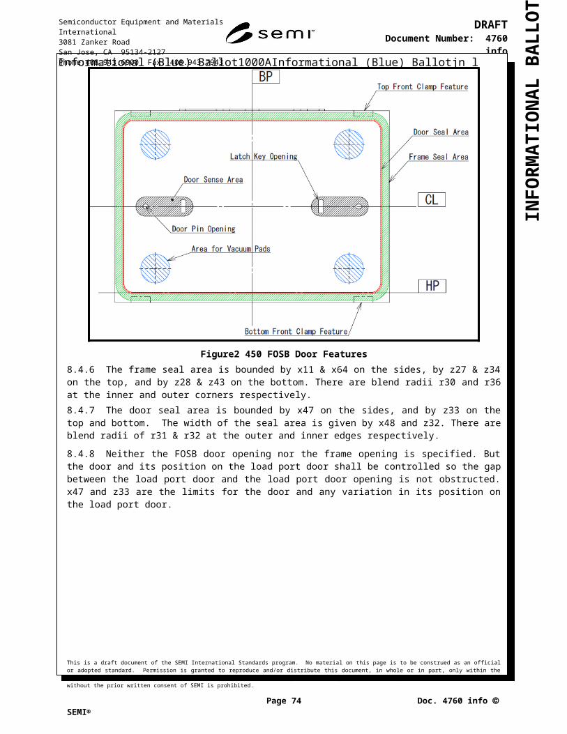
INFO
RM
ATIO
NA
L B
ALL
OT
Informational (Blue) Ballot1000AInformational (Blue) Ballotjn lFigure212D Code Placement Area on Box Shell
Figure222D Code Placement Area on Door
8.24.1 The 2D codes are not intended to be used for automated reading on fab equipment load ports, since readers would likely conflict with spaces reserved for other purposes.
8.25 2D Code — A square data matrix with a size of 8 ± 2mm consisting of 18 rows and 18 columns shall be employed on the surface of FOSB with laser marking. Each data matrix includes information designated as “primary upper case alphanumeric” per Data Matrix ECC200 Symbol of ISO/IEC 16022 with a capacity of 25 alphanumerical characters in total. These 25 characters shall contain the following 6 elements:
Character 1–2 FOSB maker; See SEMI AUX16 - List of carrier maker Identification Codes Character 3 Door-Type; Auto (A) Character 4 Location; Box Shell (B) or Door (D) Character 5–8 Model code as defined by each FOSB maker Character 9 Mold Revision number Character 10–25 FOSB Serial number
This is a draft document of the SEMI International Standards program. No material on this page is to be construed as an official or adopted standard. Permission is granted to reproduce and/or distribute this document, in whole or in part, only within the scope of SEMI International Standards committee (document development) activity. All other reproduction and/or distribution without the prior written consent of SEMI is prohibited.
Page 75 Doc. 4760 info SEMI
Semiconductor Equipment and Materials International3081 Zanker RoadSan Jose, CA 95134-2127Phone:408.943.6900 Fax: 408.943.7943
DRAFTDocument Number: 4760 info
Date: 2009/08/13

INFO
RM
ATIO
NA
L B
ALL
OT
Informational (Blue) Ballot1000AInformational (Blue) Ballotjn l
Table 1 450FOSB Dimensions Note: All linear dimensions are in mm, all angular dimensions are in degrees.
Symbol Used Figure Value Specified Datum Measured From Feature Measured To
θ1 9 45 ±6 degrees Vertical (BP & FP) Angle from vertical of the planar surfaces of kinematic coupling grooves
θ3 16 30.0 ±2 degrees HP Incline of hold-down featureθ4 14 45 ±0.5 degrees Vertical (BP & FP) Edge of automation flange centering
featureθ5 14 45 ±0.5 degrees Perpendicular to Side surface
of automation flangeSide surfaces of automation flange notches
θ6 13,15 45 ±0.5 degrees FP Side of forklift retainer feature
(d2) 3,14 (17) Automation flange centering feature (x63, y54)
Diameter at bottom of depression
d3 14 51 ±0.5 Automation flange centering feature (x63, y54)
Diameter at top of depression
(d4) 4 (10.6) x45,CL Diameter of door pin opening(d7) 5 (10.6) (x43 & x42), CL Diameter of slot for Door Pin
f001 ¶ 8.17.2.1 ≥ 175 N Applied at any point, in any direction
Force that the any one hold down feature that the carrier must withstand.
f002 ¶ 8.17.2.2 ≥ 141 N Force applied to hold down feature
Force that carrier must withstand during door opening and closing without a negative impact on the intended function of the carrier.
f230 ¶ 8.4.14 ≤ 1.7 Nm Latch Key Torque required to operate latches (each latch key)
f234 ¶ 8.4.13 ≤ 387 N Door Force to close carrier door
r6 7,12 ≥ 245 Origin Rear boundary of EE exclusion arear7 16 ≥ 30 x26, y29 Space in hold-down featurer10 6,13 ≤ 314 Origin Outer limit of carrier r12 11 227 +1/-0 x=0, y14 Radius of wafer set-down volumer13 10 ≤ 226 Origin Radius of wafer pick-up volumer15 None ≥ 15 N/A Lead in: Correctable 450 FOSB
misalignment in any horizontal direction
r18 11 ≥ r12 + 1 Origin Radius of wafer extraction volumer21 17 ≥ 10 Center of Info, placement and
Lock-Out padsExtent of pad area
r23 4,5 ≥ 14 latch key Clearancer28 4 ≥ 30 x38,z31 Area reserved for vacuum padsr29 4 ≥ 20 x44, CL & x45, CL Boundary of door sense arear30 3 ≤23 Blend radius Corners of frame seal area r31 4 ≥21 Blend radius Outer edge of door seal area r32 4 ≥19 Blend radius Inner edge of door seal arear36 3 ≤36 Blend radius Corners of frame seal arear37 7 ≥ 229 Origin Side boundary of EE exclusion arear40 ¶ 8.3 1mm maximum Not applicable All concave features (radius)
This is a draft document of the SEMI International Standards program. No material on this page is to be construed as an official or adopted standard. Permission is granted to reproduce and/or distribute this document, in whole or in part, only within the scope of SEMI International Standards committee (document development) activity. All other reproduction and/or distribution without the prior written consent of SEMI is prohibited.
Page 76 Doc. 4760 info SEMI
Semiconductor Equipment and Materials International3081 Zanker RoadSan Jose, CA 95134-2127Phone:408.943.6900 Fax: 408.943.7943
DRAFTDocument Number: 4760 info
Date: 2009/08/13

INFO
RM
ATIO
NA
L B
ALL
OT
Informational (Blue) Ballot1000AInformational (Blue) Ballotjn lSymbol Used Figure Value Specified Datum Measured From Feature Measured To
r41 ¶ 8.3 2mm maximum Not applicable All required concave features (radius)
(x1) 1, 3,9 (≤567.6) n/a Overall width of carrierx2 3,13 ≤ 283.8 BP Outer edge of carrierx3 14 300 ±0.5 Right side of automation flange Left side of automation flangex4 9 150 ±1 BP Right Edge of automation flange on
carrierx9 17 ≤220 BP Outer Edge of presence sense areax10 17 193 ±1 BP Outer center of placement sense pad
x11 3 ≤268.8 BP Inner edge of frame seal areax12 7,12 ≥ 243.5 BP Inner edge of End Effector exclusion
area x13 7,12 ≥ 135 BP Inner extent of wafer support surface x14 7,12 ≤ 50 BP Extent of rear wafer support structurex15 13,15 ≥ 250 BP Outer side of top front clamping
featurex16 13,15 ≤ 210 BP Inner side of top front clamping
featurex17 13,15 ≤ 260.0 BP Inner side of forklift feature x20 17 ≤160 BP Inner edge of side presence sense areax21 17 141 ±1 BP Outer center of placement sense padx22 17 ≥30 BP Edge of central presence sense padx23 17 55 ±1 BP Center of rear placement sense padx24 17 55 ±1 BP Center of lock-out pad (1 left / 2 right)x25 17 85 ±1 BP Center of Info Pad (A left / D right)x26 17 115 ±1 BP Center of Info Pad (B left / E right)x27 17 145 ±1 BP Center of info Pad (C left / F right)x28 16 50 ±0.5 BP Center of hold-down featurex29 20 25±1 BP Side of RFID placement volumex30 14 50 ±0.5 Right side of automation flange Automation Flange Notchx31 14 210 ±0.5 Right side of automation flange Automation Flange Notchx32 14 12 ±1 Edge of flange Automation Flange chamferx33 14 250 ±0.5 Right side of automation flange Automation Flange Notchx34 9 ≤ 132 BP Side of automation flange neckx35 13,15 14 ±0.5 Outer edge of carrier Depth of notch for forkliftx38 4,5 ≥ 10 Centered at x44, CL Width of latch key clearancex42 5 ≥3.0 Centered at x43 Length of slot for door pin(x43) 5 (220) BP Center of slot for right door pin r22(x44) 4,5 (142) BP Latch key opening(x45) 4 (220) BP Left door pin openingx47 4 ≤266.8 BP Outer edge of door seal areax48 4 ≥2 Outer edge of door seal area Inner edge of door seal areax49 4 200 BP Space reserved for vacuum padsx50 9 ≥ 229 BP Inner wall of carrierx56 14 14 ±0.5 Edge of automation flange depth of notchesx57 16 ≥250 BP Outer side of bottom front clamp
This is a draft document of the SEMI International Standards program. No material on this page is to be construed as an official or adopted standard. Permission is granted to reproduce and/or distribute this document, in whole or in part, only within the scope of SEMI International Standards committee (document development) activity. All other reproduction and/or distribution without the prior written consent of SEMI is prohibited.
Page 77 Doc. 4760 info SEMI
Semiconductor Equipment and Materials International3081 Zanker RoadSan Jose, CA 95134-2127Phone:408.943.6900 Fax: 408.943.7943
DRAFTDocument Number: 4760 info
Date: 2009/08/13

INFO
RM
ATIO
NA
L B
ALL
OT
Informational (Blue) Ballot1000AInformational (Blue) Ballotjn lSymbol Used Figure Value Specified Datum Measured From Feature Measured To
x58 16 ≤ 210 BP Inner side of bottom front clampx61 17 154 ±1 BP Inner center of placement sense padx62 17 102 ±1 BP Inner center of placement sense padx63 14 150 ±0.5 Right Side of automation
flangeFront Notch and center of d3
x64 3 ≥281.8 BP Outer side of frame seal areax66 13,15 276.0 ±1 BP Outer surface of fork lift featurex70 21 110 BP edge of 2D-code indication area on
bodyx71 21 60 BP edge of 2D-code indication area on
bodyx72 22 175 BP edge of 2D-code indication area on
doorx73 22 225 BP edge of 2D-code indication area on
door
(y1) 1, (≤502.5) n/a Overall depth of carriery2 8,13 ≤ 245 FP Rear of carriery3 14 300 ±0.5 Front side of automation flange Rear side of automation flange y4 8,13 257.0 ±0.5at
door and frame seal area and at reserved spaces for vacuum application and at Door sense area and 257.5mm maximum elsewhere on door or box shell
FP FOSB Front
y8 7,12 ≤ 180 FP Inner extent of End Effector exclusion area between x12 and x13
y9 12 ≥ 211.25 FP Inner surface of doory10 6 3.00 ±0.25 Front surface of door (y4) Space for unobstructed rotation of
latch keysy11 7,12 ≥ 200 FP Extent of rear wafer support structurey12 8 162 ±1 FP Front edge of automation flangey14 7 >1.0, ≤3.0 FP Center of r12 and r18
y19 7,8,12 ≥ 228 FP Inner extent of End Effector exclusion area near rear wafer support structure
y21 17 ≥ 30 FP Edges of side presence sense areay22 17 151 ±1 FP Outer center of placement sense pady23 17 74 ±1 FP Outer center of placement sense pady24 17 120 ±1 FP Row of Info and Lock Out padsy25 17 194 ±1 FP Center of rear placement sense padsy26 19 ≥ 225 FP Front of RFID placement volumey27 19 ≤ 230 FP Rear of RFID placement volumey28 14 12 ±1 Edge of Automation Flange Automation Flange chamfer
This is a draft document of the SEMI International Standards program. No material on this page is to be construed as an official or adopted standard. Permission is granted to reproduce and/or distribute this document, in whole or in part, only within the scope of SEMI International Standards committee (document development) activity. All other reproduction and/or distribution without the prior written consent of SEMI is prohibited.
Page 78 Doc. 4760 info SEMI
Semiconductor Equipment and Materials International3081 Zanker RoadSan Jose, CA 95134-2127Phone:408.943.6900 Fax: 408.943.7943
DRAFTDocument Number: 4760 info
Date: 2009/08/13

INFO
RM
ATIO
NA
L B
ALL
OT
Informational (Blue) Ballot1000AInformational (Blue) Ballotjn lSymbol Used Figure Value Specified Datum Measured From Feature Measured To
y29 14 90 ±0.5 Front side of automation flange Automation Flange Notchy30 8 ≥ 195.75 FP Back of door flangey31 14 14 ±0.5 Side of automation flange Depth of notchesy34 16 90 ±0.5 FP Front edge of hold-down openingy35 16 60 ±0.5 FP Rear edge of hold-down openingy37 14 ≤ 144 FP Front side of automation flange necky38 16 75 ±0.5 FP Center of hold-down featurey39 6 ≥ 12 Front Surface of Door Clearance for Latchkeysy40 6 ≥ 12 Front Surface of Door Clearance for Door Piny43 13,15 3.5 ±0.5 Front Surface of FOSB Frame Front side of Top front clampingy44 13,15 ≤ 233.5 FP Rear side of Top front clamping y45 13,15 ≥150 FP Front side of forklift featurey46 13,15 ≥120 FP Rear limit of surface for forklifty47 15,16 3.5 ±0.5 Front Surface of FOSB Frame Front side of bottom front clampingy48 15,16 ≤233.5 FP Rear side of bottom front clampingy50 17 95 ±1 FP Placement Sense Pad for forklifty52 17 125 ±1 FP Inner center of placement sense pady53 17 48 ±1 FP Inner center of placement sense pady54 14 150 ±0.5 Front of automation flange Notch and center of d3y55 8 ≤196.25 FP Rear of wafer mapping exclusion
volumey56 8,14 ≤120 FP Rear side of automation flange neckY60 7 ≥100 FP Rear of wafer retainingy70 21 170 FP edge of 2D-code indication area on
bodyy71 21 210 FP Edge of 2D-code indication area on
body
(z1) 1,8,9 (≤404.0) n/a Over all height of carrierz2 8 ≥17 Top of automation flange Bottom of centering depressionz5 15 ≥12 Top of Door Frame Bottom of upper front clamp featurez6 16 11 ±0.5 HP Lower horizontal surface inside hold-
down featurez7 16 6 ±0.2 Lower horizontal surface inside
hold-down featureLower edge of hold-own incline
z8 1,8,9 382.0±1 HP Top of carrierz9 8,9,14 ≥ 21 Bottom surface of automation
flangeClearance for use of automation flange
z11 8,9,18 ≤21 HP FOSB bottom surface areas not otherwise specified
z13 9,14 7.5 ±0.5 Top surface of automation flange
Bottom surface of automation flange
z14 8 43.6 ±0 HP Bottom nominal wafer seating planez15 8 ≥ 11.1 Height of first wafer slot top Clearance below top of first wafer slotz16 10 ≥ 7.1 Top surface of each nominal
wafer seating planeBottom surface of next higher wafer support
z17 10 11.1 ±0 Each nominal wafer seating plane
Adjacent nominal wafer seating planes (wafer pitch)
This is a draft document of the SEMI International Standards program. No material on this page is to be construed as an official or adopted standard. Permission is granted to reproduce and/or distribute this document, in whole or in part, only within the scope of SEMI International Standards committee (document development) activity. All other reproduction and/or distribution without the prior written consent of SEMI is prohibited.
Page 79 Doc. 4760 info SEMI
Semiconductor Equipment and Materials International3081 Zanker RoadSan Jose, CA 95134-2127Phone:408.943.6900 Fax: 408.943.7943
DRAFTDocument Number: 4760 info
Date: 2009/08/13

INFO
RM
ATIO
NA
L B
ALL
OT
Informational (Blue) Ballot1000AInformational (Blue) Ballotjn lSymbol Used Figure Value Specified Datum Measured From Feature Measured To
z18 8 ≥ 7.1 Top surface of top wafer slot Any point above top nominal wafer seating plane
z19 15 163 ±1 HP Top of forklift featurez20 15 ≥10 Top of forklift feature Bottom of forklift retainer featurez21 10 0 ±0.5 Each nominal wafer seating
planeEach actual nominal wafer seating plane
z22 11 4.85 z49 above each nominal wafer seating plane
Top of wafer extraction and wafer set-down volumes
z23 18 20 ±0.5 HP Surface of placement sense padsz24 18 ≤ 15 HP Top of space within Lockout & Info
pads when not activez25 8 ≥17.0 Top of wafer 25 nominal
supportTop of wafer mapping exclusion volume
z26 8 ≥24.1 HP Bottom of wafer mapping exclusion volume
z27 3 ≥195.3 CL Top of frame seal areaz28 3 ≥195.3 CL Bottom of frame seal areaz30 4 179.3 HP CL – Horizontal Center Line of the
doorz31 4 129 CL Center of space reserved for vacuum
padsz32 4 ≥2 Outer edge of door seal area Inner edge of Door seal areaz33 4 ≤180.3 CL Outer edge of door seal areaz34 3 ≤182.3 CL Inner edges of frame seal area z35 15 ≤74 HP Bottom of forklift featurez36 15 ≥12 Bottom of door frame Top of lower front clamp featurez37 20 ≥ 5 HP Bottom of RFID placement volumez38 20 ≤10 HP Top of RFID placement volumez42 3 ≤21 HP Bottom of door flange
z43 3,8 378.6±1 HP Top of door flange(z44) 3,8 (≤364.6) n/a Height of door opening(z45) 3 (400.6) n/a Height of door flangez48 16 ≥ 11 Lower horizontal surface inside
hold-down featureUpper horizontal surface inside hold-down feature
z49 11 1.5 Each nominal wafer seating plane
Bottom of wafer extraction volume. (To center the extraction volume between slots)
z50 18 20 ±1 HP Height of info and lockout pads when active
z70 22 230 HP edge of 2D-code indication area on door
z71 22 270 HP edge of 2D-code indication area on door
* Unless otherwise noted, all dimensions are in mm. Reference dimensions are in parentheses and are not requirements.Measured values for dimensions without specified tolerance should be rounded up or down to the last significant figure of the dimension in accordance with good engineering practice.Measured values for dimensions with specified tolerances should be rounded up or down to the last significant figure of the tolerance in accordance with good engineering practice.
This is a draft document of the SEMI International Standards program. No material on this page is to be construed as an official or adopted standard. Permission is granted to reproduce and/or distribute this document, in whole or in part, only within the scope of SEMI International Standards committee (document development) activity. All other reproduction and/or distribution without the prior written consent of SEMI is prohibited.
Page 80 Doc. 4760 info SEMI
Semiconductor Equipment and Materials International3081 Zanker RoadSan Jose, CA 95134-2127Phone:408.943.6900 Fax: 408.943.7943
DRAFTDocument Number: 4760 info
Date: 2009/08/13

INFO
RM
ATIO
NA
L B
ALL
OT
Informational (Blue) Ballot1000AInformational (Blue) Ballotjn lTable 2 Derivation of Reference DimensionsSymbol Used Value Formula(x1) (≤ 567.6) x2 + x2 (≤ 283.8 + ≤ 283.8)(y1) (≤ 502.5) y2 + y4max (≤ 245 + 257.5)(z1) (≤ 404.0) z8 max + z11 (383.0 + 21.0)(z44) (364.6) z34 + z34 (182.3 + 182.3)(z45) (400.7) z42 + z43max (21.0 + 379.7)
NOTICE: SEMI makes no warranties or representations as to the suitability of the standard(s) set forth herein for any particular application. The determination of the suitability of the standard(s) is solely the responsibility of the user. Users are cautioned to refer to manufacturer’s instructions, product labels, product data sheets, and other relevant literature respecting any materials or equipment mentioned herein. These standards are subject to change without notice.
By publication of this standard, Semiconductor Equipment and Materials International (SEMI) takes no position respecting the validity of any patent rights or copyrights asserted in connection with any item mentioned in this standard. Users of this standard are expressly advised that determination of any such patent rights or copyrights, and the risk of infringement of such rights are entirely their own responsibility.
This is a draft document of the SEMI International Standards program. No material on this page is to be construed as an official or adopted standard. Permission is granted to reproduce and/or distribute this document, in whole or in part, only within the scope of SEMI International Standards committee (document development) activity. All other reproduction and/or distribution without the prior written consent of SEMI is prohibited.
Page 81 Doc. 4760 info SEMI
Semiconductor Equipment and Materials International3081 Zanker RoadSan Jose, CA 95134-2127Phone:408.943.6900 Fax: 408.943.7943
DRAFTDocument Number: 4760 info
Date: 2009/08/13