vidyarthiplus - fmcetfmcet.in/eee/ee2255_auque.pdfdiscuss in brief about the design procedure of an...
TRANSCRIPT


vidyarthiplus.com
vidyarthiplus.com
vidyarthiplus.com

ANNA UNIVERSITY- COMBATORE
B.E./ B.TECH. DEGREE EXAMINATION - JUNE 2009.
ELECTRICAL & ELECTONICS ENGG. - FOURTH SEMESTER
PART-A
Answer all questions. (20*2=40)
1. State De-Morgans theorem.
2. Briefly explain the streamlined method of converting binary to decimal number
with example.
3. Give the Gray code for the binary number (111)2.
4. Subtract the following:0101 1011-0000 0101.
5. Draw a 1 to 16 demultiplexer circuit.
6. What is priority encoder.
7. Show the common-cathode type of seven segment indicator.
8. Design a half adder using NAND gates only.
9. Draw the truth table for a NOR gate RS flip flop.
10. Obtain D flip flop from JK flip flop.
11. Differentiate synchronous counter and Asynchronous counter.
12. Draw a modulo 6 counter.hat is saturation delay time? Explain.
13. Compare bipolar family transistors with MOS family transistors.
14. what is race condition? How can it be eliminated?
15. What is essential hazard? Give an example.
16. Compare volatile data storage with non volatile data storage.
17. How is combinational logic generated in FPGA.
18. What is a DRAM? How is it refreshed?
19. Draw a macrocell of PLD.
www.eeecube.blogspot.com
www.eeecube.blogspot.com
DIGITAL LOGIC CIRCUITS

PART-B
Answer any five. (5*12=60)
1. Simplify the following Boolean expression using three variable maps:
a) XY+X'Y'Z'+X'YZ'
b) X'Y'+YZ+X'YZ'
c) X'Y+YZ+Y'Z
2. Design a 3-bit parity generator circuit and the circuit of a 4-bit parity checker
using even and odd parity bit.
3. Discuss in detail about state reduction problem and state assignment problem.
4. Explain the operation of clocked masterslave JK flipflop and D flipflop with neat
digrams.
5. Discuss in brief about the design procedure of an asychronous circuits starting
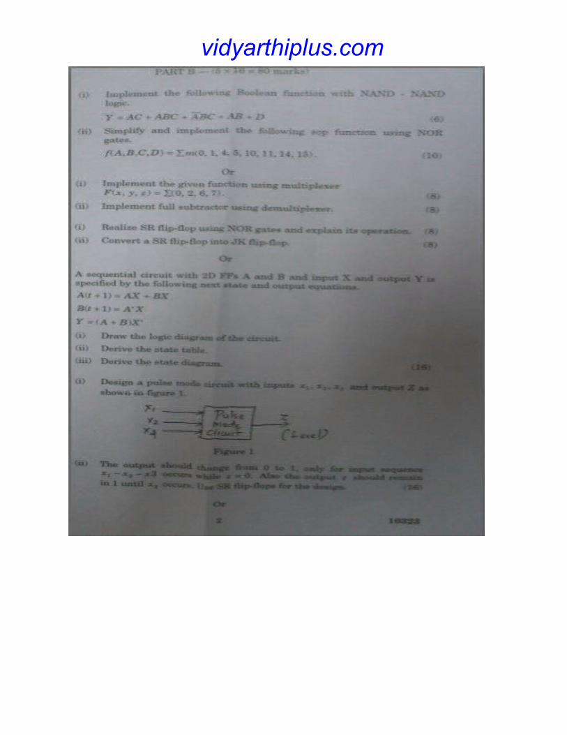
from the statement of the problem and culminates in a logic diagram.
6. Explain with a suitable example the procedure for analyzing a synchronous
sequential circuit with SR latches.
7. Write short notes on :
a) PAL
b) FPGA
8. Discuss in detail about the types of Read only memories.
www.eeecube.blogspot.com
www.eeecube.blogspot.com

www.eeecube.blogspot.com
www.ee
ecube.b
logsp
ot.com
Reg. No. :
B.E./B.Tech. DEGREE EXAMINATION, APRIL/MAY 2010
Fourth Semester
Electrical and Electronics Engineering
EE2255 — DIGITAL LOGIC CIRCUITS
(Regulation 2008)
Time: Three hours Maximum: 100 Marks
Answer ALL Questions
PART A — (10 × 2 = 20 Marks)
1. Show that
(a) babaa +=+ '
(b) '''''' xyzxxyyzxzyx +=++ .
2. Draw the Truth table and logic circuit of half adder.
3. Draw the circuit of SR Flip flop.
4. What are synchronous sequential circuits?
5. Give the characteristic equation and state diagram of JK flip flop.
6. What is a self starting counter?
7. What is the advantage of PLA over ROM?
8. Which IC family offers (a) low propagation delay, and (b) low power dissipation?
9. Write HDL for half adder.
10. What are the various modeling techniques in HDL?
Question Paper Code: E3090
www.eeecube.blogspot.com
www.ee
ecube.b
logsp
ot.com
E 3090 2
PART B — (5 × 16 = 80 Marks)
11. (a) (i) Simplify using k-map
)14,13,12,9,8,6,5,4,2,1,0(),,,( ∑=zyxwF . (8)
(ii) Design a BCD to Excess-3 code converter. (8)
Or
(b) (i) Solve )13,12,10,8,0()11,6,4,3,1(),,,( dmzyxwg ∑+∑= . (8)
(ii) Design a decimal adder to add two decimal digits. (8)
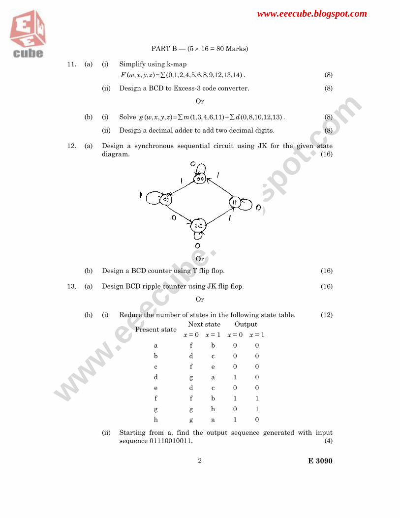
12. (a) Design a synchronous sequential circuit using JK for the given state
diagram. (16)
Or
(b) Design a BCD counter using T flip flop. (16)
13. (a) Design BCD ripple counter using JK flip flop. (16)
Or
(b) (i) Reduce the number of states in the following state table. (12)
Present state Next state Output
x = 0 x = 1 x = 0 x = 1
a f b 0 0
b d c 0 0
c f e 0 0
d g a 1 0
e d c 0 0
f f b 1 1
g g h 0 1
h g a 1 0
(ii) Starting from a, find the output sequence generated with input
sequence 01110010011. (4)
www.eeecube.blogspot.com
www.ee
ecube.b
logsp
ot.com
E 3090 3
14. (a) (i) Design a combinatorial circuit using ROM. The circuit accepts 3-bit
number and generates an output binary number equal to square of
input number. (8)
(ii) Repeat the above problem using PLA. (8)
Or
(b) (i) Compare all the IC logic families based on
(1) Power consumption
(2) Fan out
(3) Power dissipation
(4) Propagation delay
(5) Switching speed
(6) Noise margin. (8)
(ii) Describe the different types of memories. (8)
Or
(b) (i) Write an HDL behavioral description of JK flip flop using if-else
statement based on the value of present state. (8)
(ii) Draw the logic diagram for the following module. (8)
module seqcrt (A, B, C, Q, CLK) ;
input A, B, C, CLK ;
output Q ;
reg Q, E ;
always @ (Posedge CLK)
begin
E < = A & B ;
Q < = E/C ;
end
end module
————––––——

www.eeecube.blogspot.com
www.ee
ecube.b
logsp
ot.com
Reg. No. :
B.E./B.Tech. DEGREE EXAMINATION, APRIL/MAY 2011
Fourth Semester
Electrical and Electronics Engineering
EE 2255 — DIGITAL LOGIC CIRCUITS
(Regulation 2008)
Time : Three hours Maximum : 100 marks
Answer ALL questions
PART A — (10 × 2 = 20 marks)
1. State DeMorgan's theorem.
2. Why is MUX called as data selector?
3. Write the excitation table for JK flip flop.
4. Write the characteristics table for SR flip flop.
5. State the hazards in asynchronous sequential circuits.
6. What is the difference between asynchronous and synchronous sequential
circuits?
7. Name the types of ROM.
8. Define fan in and fan out characteristics of digital logic families.
9. What are ASM?
10. When can RTL be used to represent digital systems?
Question Paper Code : 11315

www.eeecube.blogspot.com
www.ee
ecube.b
logsp
ot.com
11315 2
PART B — (5 × 16 = 80 marks)
11. (a) (i) Reduce the given expressions using Boolean algebra :
(1) xyzzyxyzxzyxzyx +′+′+′′+′′′
(2) abcbcacbacab +′+′+′
(3) rqprpqqrprqprqp ′′+′+′+′′+′ ' . (12)
(ii) For the given circuit, derive an algebraic expression in SOP form :
(4)
Or
(b) (i) Reduce the following expression using k-map. (6)
xyzwwxzzwxyxzwzyxf ′++′+′+′′= .
(ii) Implement a full adder circuit with
(1) Decoder
(2) Multiplexer. (10)
12. (a) Draw the state diagram. Derive the state equation and draw the clocked
sequential circuit for the following state table. (16)
Next state Output
Present state x = 0 x = 1 x = 0 x = 1
AB AB AB Y Y
00 00 01 0 0
01 11 01 0 0
10 10 00 0 0
11 10 11 0 0
Or
(b) Design BCD counter using T flip flops, where flip flop inputs are
421 ,, TQTQTQ and 8TQ . (16)

www.eeecube.blogspot.com
www.ee
ecube.b
logsp
ot.com
11315 3
13. (a) Design an asynchronous BCD counter. (16)
Or
(b) Describe the steps involved in design of asynchronous sequential circuit
in detail with an example. (16)
14. (a) (i) Implement the following two Boolean functions with a PLA :
).7,6,5,0(),,(
)4,2,1,0(),,(
2
1
∑=
∑=
CBAF
CBAF
(10)
(ii) Describe the characteristics of all types of memories. (6)
Or
(b) (i) Write notes on digital logic families. (9)
(ii) Design ROM for the following functions.
)2,0(;)3,2,1( 21 ∑=∑= FF . (7)
15. (a) Write the VHDL code for mod 6 counter. (16)
Or
(b) Describe the RTL in VHDL. (16)
——————
www.eeecube.blogspot.com
www.ee
ecube.b
logsp
ot.com
B.E./B.Tech. DEGREE EXAMINATION, NOVEMBER/DECEMBER 2010
Fourth Semester
Electrical and Electronics Engineering
EE 2255 — DIGITAL LOGIC CIRCUITS
(Regulation 2008)
Time : Three hours Maximum : 100 Marks
Answer ALL questions
PART A — (10 × 2 = 20 Marks)
1. Show that Excess-3 code is self complementing.
2. Add the hexadecimal numbers: 93 and DE.
3. Convert JK flip-flop to T-flip-flop.
4. Mention the major application of Master Slave FF.
5. Draw the state diagram of SR Flip Flop.
6. Define asynchronous sequential machine.
7. State the important characteristics of TTL family.
8. In which type of TTL gate wired ANS logic is possible?
9. Write the VHDL code for AND gate.
10. List the operators available in VHDL.
PART B — (5 × 16 = 80 Marks)
11. (a) Reduce the following using tabulation method and verify with K maps.
( ) ( ) ∑ = 14 , 12 , 10 , 8 , 6 , 4 , 3 , 2 , 1 , 0 , , , D C B A F
Or
www.eeecube.blogspot.com
www.ee
ecube.b
logsp
ot.com
(b) Obtain the minimum SOP using Quine Mcclusky’s method and verify
using ‘K’ map for the following.
m13 m12 m11 m10 m9 m8 m4 m2 m0
12. (a) Design a counter with the sequence 0, 1, 3, 7, 6, 4, 0.
Or
(b) The following sequence is to be realized by a counter consisting of
3 JKFF’s.
A1 0 0 0 0 1 1 0
A2 0 1 1 0 0 1 0
A3 0 1 0 1 1 0 0
Design the counter.
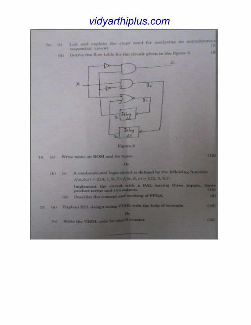
13. (a) (i) List and explain the steps used for analyzing an asynchronous
sequential circuit. (8)
(ii) Describe procedure to get state table from excitation table in an
asynchronous sequential circuit. How does it differ from
synchronous sequential circuit? (8)
Or
(b) (i) How do you get output specifications from a flow table in
asynchronous sequential circuit operating in fundamental mode? (6)
(ii) When do you get the critical and non-critical races? How will you
obtain race free conditions? (10)
14. (a) (i) Explain the concept, working and characteristics of TTL logic
families. (8)
(ii) What do you understand by FPGA? Explain the operation and
applications? (8)
Or
(b) (i) Describe the working of EPROM. List the applications of EPROM.
www.eeecube.blogspot.com
www.ee
ecube.b
logsp
ot.com
(8)
(ii) Discuss on the concept, operation and characteristics of CMOS
technology. (8)
15. (a) Construct a VHDL module listing for a 16:1 MUX that is based on the
assign statement. Use a 4-bit select word S3 S2 S1 S0 to map the selected
input Pi (i = 0,...15) to the output.
Or
(b) (i) Explain the design procedure of RTL using VHDL. (10)
(ii) Write a note on VHDL test benches. (6)

www.eeecube.blogspot.com
www.ee
ecube.b
logsp
ot.com
Reg. No. :
B.E./B.Tech. DEGREE EXAMINATION, NOVEMBER/DECEMBER 2011.
Fourth Semester
Electrical and Electronics Engineering
EE 2255 — DIGITAL LOGIC CIRCUITS
(Regulation 2008)
Time : Three hours Maximum : 100 marks
Answer ALL questions.
PART A — (10 × 2 = 20 marks)
1. How does don’t care condition in k -map help for circuit simplification?
2. What is the difference between decoder and demultiplexer?
3. What is race around condition in Flipflops?
4. How does the state transition diagram of a Moore model differ from Mealy
model?
5. What are hazards in asynchronous sequential circuits?
6. What is fundamental mode of operation in asynchronous sequential
circuits?
7. What is FPGA?
8. Why should we take care while using CMOS devices?
9. What are the operators present in VHDL?
10. What is the meaning of the following RTL Statement?
T1 : ACC ← ACC and MDR.
Question Paper Code : 55361

www.eeecube.blogspot.com
www.ee
ecube.b
logsp
ot.com
55361 2
PART B — (5 × 16 = 80 marks)
11. (a) Give the simplified expression for the following logic equation where
d represents don’t care condition.
( ) ( ) ( )14,10,7,4,2,115,12,11,8,0,,, dmDCBAf +Σ=
Represent the simplified expression using logic gates. (16)
Or
(b) Write brief notes on the following :
(i) DeMorgan’s theorem (4)
(ii) Comparators (4)
(iii) Binary to gray code converter (4)
(iv) Multiplexer. (4)
12. (a) Draw the state transition diagram of a sequence detector circuit that
detects ‘1010’ from input data stream using Moore model Mealy
model.
(16)
Or
(b) Design a counter using JK flipflop for realizing the following
sequence.
(16)
Q2 Q1 Q
0
0 0 0
0 0 1
0 1 1
1 1 1
1 1 0
1 0 0
0 0 0
13. (a) (i) When does oscillation occur in an asynchronous sequential
logic circuit? (4)
(ii) Draw and explain the state transition diagram of modulo-6
counter in asynchronous sequential logic. (12)
www.eeecube.blogspot.com
www.ee
ecube.b
logsp
ot.com
55361 3
Or
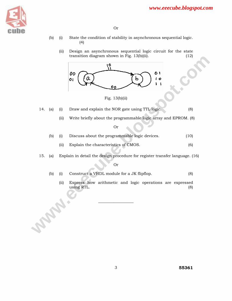
(b) (i) State the condition of stability in asynchronous sequential logic. (4)
(ii) Design an asynchronous sequential logic circuit for the state transition diagram shown in Fig. 13(b)(ii). (12)
Fig. 13(b)(ii)
14. (a) (i) Draw and explain the NOR gate using TTL logic. (8)
(ii) Write briefly about the programmable logic array and EPROM. (8)
Or
(b) (i) Discuss about the programmable logic devices. (10)
(ii) Explain the characteristics of CMOS. (6)
15. (a) Explain in detail the design procedure for register transfer language. (16)
Or
(b) (i) Construct a VHDL module for a JK flipflop. (8)
(ii) Express how arithmetic and logic operations are expressed using RTL. (8)
—————————