vcsels for high-speed, long-reach, and wavelength...
TRANSCRIPT
Thesis for the Degree of Doctor of Philosophy
VCSELs for High-Speed, Long-Reach, andWavelength-Multiplexed Optical Interconnects
Erik Haglund
Photonics LaboratoryDepartment of Microtechnology and Nanoscience (MC2)
Chalmers University of TechnologyGöteborg, Sweden, 2015
VCSELs for High-Speed, Long-Reach, andWavelength-Multiplexed Optical InterconnectsErik Haglund
Göteborg, August 2015
© Erik Haglund, 2015
ISBN 978-91-7597-255-8
Doktorsavhandlingar vid Chalmers Tekniska HögskolaNy serie 3936ISSN 0346-718X
Technical Report MC2-315ISSN 1652-0769
Photonics LaboratoryDepartment of Microtechnology and Nanoscience (MC2)Chalmers University of Technology, SE-412 96 Göteborg, SwedenPhone: +46 (0) 31 772 1000
Front cover illustration: From left to right: a 50 Gbit/s eye diagram, high-speedVCSELs on a chip, and cross-section SEM image of released free-hanging gratingbars (each bar is around 250 nm wide).
Printed by Chalmers reproservice, Chalmers University of TechnologyGöteborg, Sweden, August, 2015
VCSELs for High-Speed, Long-Reach, andWavelength-Multiplexed Optical Interconnects
Erik HaglundPhotonics Laboratory
Department of Microtechnology and Nanoscience (MC2)Chalmers University of Technology, SE-412 96 Göteborg, Sweden
AbstractThe vertical-cavity surface-emitting laser (VCSEL) is the standard light source inshort-reach fiber-optic links in datacenters and supercomputers. These systems usean enormous number of links, making cost and energy efficiency pressing issues.GaAs-based 850 nm VCSELs are therefore attractive due to low-cost fabrication, asmall device footprint enabling compact integration into 2-D arrays, and above all,the capability of high-speed direct modulation at low power consumption. However,present commercial VCSELs, operating at around 25 Gbit/s over up to 100 m ofmultimode fiber, have insufficient speed, energy-efficiency, and reach for future links.
Many of the attractive VCSEL properties stem from their small modal and activeregion volumes. The first part of this thesis explores the limits of optical and electri-cal confinement in high-speed VCSELs by using the shortest possible cavity length,and positioning the current-confining oxide aperture close to the active region. Thisenabled small-oxide-aperture VCSELs with record-high modulation bandwidth of30 GHz, capable of energy-efficient data transmission at 25-50 Gbit/s with record-low dissipated energy per bit in the VCSEL of <100 fJ/bit.
High-speed VCSELs are usually transverse multimode with large spectral widths.This leads to penalties from chromatic and modal fiber dispersion, limiting the fea-sible transmission distance to around 100 m at 25 Gbit/s, which is too short forlarge datacenters. The second part of this thesis demonstrates that VCSELs withnarrow spectral widths, realized using either a small oxide aperture or an integratedmode filter, can transmit data at high bit rates over much longer distances. VCSELswith mode filters enabled transmission at 20 Gbit/s over 2000 m, setting a bit-rate-distance product record for directly modulated 850 nm VCSEL links.
To enable higher link capacity, wavelength division multiplexing may be used,where several channels at different wavelengths are transmitted in the same fiber.The final part of the thesis presents the design, fabrication, and experimental resultsfor monolithically integrated 980 nm multi-wavelength VCSEL arrays. By usinghigh-contrast gratings with different parameters as top mirrors, the VCSEL reso-nance wavelength may be set in a post-growth process. Lasing over a wavelengthspan of 15 nm was realized.
Keywords: vertical-cavity surface-emitting laser, optical interconnect, high-speedmodulation, spectral width, oxide aperture, quasi-single-mode, mode filter, high-contrast grating, wavelength control.
i

ii
List of Papers
This thesis is based on the following appended papers:
[A] E. Haglund, P. Westbergh, J. S. Gustavsson, E. P. Haglund, A. Larsson, “High-speedVCSELs with strong confinement of optical fields and carriers,” to appear in J. ofLightwave Technol., vol. 33, no. 24, pp. 1-9, Dec. 2015, (invited paper).
[B] E. Haglund, P. Westbergh, J. S. Gustavsson, E. P. Haglund, A. Larsson, M. Geen,and A. Joel, “30 GHz bandwidth 850 nm VCSEL with sub-100 fJ/bit energy dissipationat 25-50 Gbit/s,” Electron. Lett., vol. 51, no. 14, pp. 1096-1098, July 2015.
[C] R. Safaisini, K. Szczerba, E. Haglund, P. Westbergh, J. S. Gustavsson, A. Larsson,and P. Andrekson, “20 Gbit/s error-free operation of 850 nm oxide-confined VCSELsbeyond 1 km of multimode fibre,” Electron. Lett., vol. 48, no. 19, pp. 1225-1227,Sept. 2012.
[D] R. Safaisini, K. Szczerba, P. Westbergh, E. Haglund, B. Kögel, J. S. Gustavsson,A. Larsson, and P. Andrekson, “High-Speed 850 nm quasi-single-mode VCSELs forextended-reach optical interconnects,” J. Opt. Commun. Netw., vol. 5, no. 7, pp. 686-695, July 2013.
[E] E. Haglund, Å. Haglund, P. Westbergh, J. S. Gustavsson, B. Kögel, and A. Larsson,“25 Gbit/s transmission over 500 m multimode fibre using 850 nm VCSEL with inte-grated mode filter,” Electron. Lett., vol. 48, no. 9, pp. 517-518, April 2012.
[F] E. Haglund, Å. Haglund, J. S. Gustavsson, B. Kögel, P. Westbergh, and A. Larsson,“Reducing the spectral width of high speed oxide confined VCSELs using an integratedmode filter,” Proc. of SPIE, vol. 8276, pp. 82760L1-8, Feb. 2012.
[G] R. Safaisini, E. Haglund, P. Westbergh, J. S. Gustavsson, and A. Larsson, “20 Gb/sdata transmission over 2 km multimode fibre using 850 nm mode filter VCSELs,”Electron. Lett., vol. 50, no. 1, pp. 40-42, Jan. 2014.
[H] E. Haglund, J. S. Gustavsson, J. Bengtsson, Å. Haglund, A. Larsson, D. Fattal,W. Sorin, and M. Tan, “Demonstration of post-growth wavelength setting of VCSELsusing high-contrast gratings,” submitted to Opt. Express, Aug. 2015.
iii
Related publications and conference contributions by the authornot included in the thesis:
Journal papers
[I] P. Westbergh, R. Safaisini, E. Haglund, B. Kögel, J. S. Gustavsson, A. Larsson,M. Geen, R. Lawrence, and A. Joel, “High-speed 850 nm VCSELs with 28 GHz modu-lation bandwidth operating error-free up to 44 Gbit/s,” Electron. Lett., vol. 48, no. 18,pp. 1145-1147, Aug. 2012.
[J] P. Westbergh, R. Safaisini, E. Haglund, J. S. Gustavsson, A. Larsson, M. Geen,R. Lawrence, and A. Joel, “High-speed oxide confined 850-nm VCSELs operating error-free at 40 Gb/s up to 85°C,” IEEE Photon. Techn. Lett., vol. 25, no. 8, pp. 768-771,April 2013.
[K] P. Westbergh, E. P. Haglund, E. Haglund, R. Safaisini, J. S. Gustavsson, andA. Larsson, “High-speed 850 nm VCSELs operating error free up to 57 Gbit/s,” Elec-tron. Lett., vol. 49, no. 16, pp. 1021-1023, Aug. 2013.
Conference presentations and papers
[L] P. Westbergh, E. Haglund, J. S. Gustavsson, Å. Haglund, B. Kögel, and A. Larsson,“High speed VCSELs for short reach communication,” European Semiconductor LaserWorkshop 2011, Lausanne, Switzerland, Sept. 2011.
[M] A. Larsson, J. S. Gustavsson, Å. Haglund, J. Bengtsson, B. Kögel, P. Westbergh,R. Safaisini, E. Haglund, K. Szczerba, M. Karlsson, and P. Andrekson, “High speedVCSELs for optical interconnects,” 24th International Conference on Indium Phos-phide and Related Materials 2012, Santa Barbara, CA, USA, paper Th-2C.1, Aug. 2012.
[N] A. Larsson, J. S. Gustavsson, Å. Haglund, B. Kögel, J. Bengtsson, P. Westbergh,E. Haglund, and P. P. Baveja, “High-speed tunable and fixed-wavelength VCSELs forshort-reach optical links and interconnects,” in Proc. of SPIE, vol. 8276, pp. 82760H1-9,San Francisco, CA, USA, Feb. 2012.
[O] P. Westbergh, R. Safaisini, E. Haglund, B. Kögel, J. S. Gustavsson, A. Larsson, andA. Joel, “High-speed 850 nm VCSELs with 28 GHz modulation bandwidth,” EuropeanSemiconductor Laser Workshop 2012, Brussels, Belgium, Sept. 2012.
[P] R. Safaisini, K. Szczerba, E. Haglund, P. Westbergh, J. S. Gustavsson, A. Larsson,and P. Andrekson, “22 Gb/s error-free data transmission beyond 1 km of multi-modefiber using 850 nm VCSELs,” in Proc. of SPIE, vol. 8639, pp. 86390T1-7, San Francisco,CA, USA, Feb. 2013.
[Q] P. Westbergh, R. Safaisini, E. Haglund, J. S. Gustavsson, A. Larsson, and A. Joel,“High-speed 850 nm VCSELs with 28 GHz modulation bandwidth for short reach com-munication,” in Proc. of SPIE, vol. 8639, pp. 86390X1-6, San Francisco, CA, USA,Feb. 2013.
[R] J. S. Gustavsson, A. Larsson, Å. Haglund, J. Bengtsson, P. Westbergh, R. Safaisini, andE. Haglund, “High speed 850nm VCSELs for >40Gb/s transmission,” in Optical FiberCommuniation Conference (OFC) 2013, San Francisco, CA, USA, paper OTh4H.4,Feb. 2013.
[S] P. Westbergh, R. Safaisini, E. Haglund, J. S. Gustavsson, A. Larsson, and A. Joel,“High speed oxide confined 850 nm VCSELs operating error-free at 47 Gbit/s at room
iv
temperature and 40 Gbit/s at 85°C,” Conference of Lasers and Electro-Optics (CLEO)Europe, Munich, Germany, paper CB-7.1, May 2013.
[T] J. S. Gustavsson, A. Larsson, Å. Haglund, J. Bengtsson, P. Westbergh, R. Safaisini,and E. Haglund, “High-speed, high-temperature VCSELs for optical interconnects,”in IEEE Photonic Society Summer Topical Meeting Series 2013, Waikoloa, HI, USA,paper MA2.2, July 2013.
[U] E. Haglund, P. Westbergh, E. P. Haglund, R. Safaisini, J. S. Gustavsson, K. Szczerba,Å. Haglund, and A. Larsson, “850 nm datacom VCSELs for higher-speed and longer-reach transmission,” European VCSEL Day, Lausanne, Switzerland, June 2013.
[V] A. Larsson, P. Westbergh, J. S. Gustavsson, E. Haglund, and E. P. Haglund, “Highspeed VCSELs and VCSEL arrays for single and multicore fiber interconnects,” in Proc.of SPIE, vol. 9381, pp. 93810D1-11, San Francisco, CA, USA, Feb. 2015.
[W] S. Kumari, J. S. Gustavsson, R. Wang, E. P. Haglund, P. Westbergh, D. Sanchez,E. Haglund, Å. Haglund, J. Bengtsson, N. Le Thomas, G. Roelkens, A. Larsson,and R. Baets, “Integration of GaAs-based VCSEL array on SiN platform with HCGreflectors for WDM applications,” in Proc. of SPIE, vol. 9372, pp. 93720U1-7, SanFrancisco, CA, USA, Feb. 2015.
[X] E. Haglund, P. Westbergh, J. S. Gustavsson, E. P. Haglund, A. Larsson, M. Geen, andA. Joel, “High-speed 850 nm VCSEL with 30 GHz modulation bandwidth,” Confer-ence of Lasers and Electro-Optics (CLEO) Europe, Munich, Germany, paper CB-2.4,June 2015.
Other publications
[Y] E. Haglund, Å. Haglund, P. Westbergh, J. S. Gustavsson, B. Kögel, and A. Larsson,“Mode-filtered semiconductor lasers enable longer-reach optical interconnects,” SPIENewsroom, Oct. 2012.
v

vi
Acknowledgement
There are many who have supported me during the last five years, making thiswork possible. I would first like to thank my supervisor and examiner Prof.Anders Larsson for letting me work in this exciting field, and for his friendlysupport, with a door always open for discussions. I would like to thank ÅsaHaglund for cheerfully sharing her vast experience in VCSELs, and also for,together with Petter Westbergh, giving me an excellent introduction to thefine art of VCSEL processing. However, no VCSELs would have been fabri-cated without the outstanding Nanofabrication Laboratory staff, working end-lessly to keep our magnificent cleanroom running. I am also grateful to JohanS. Gustavsson and Jörgen Bengtsson for simulations of VCSELs and HCGs,Rashid Safaisini for collaboration on difficult projects, Krzysztof Szczerba foranswering any question in the world, Benjamin Kögel for teaching me aboutcourage, and Emanuel Haglund for discussions about everything from shavingto VCSELs. My office mates Martin Stattin and Attila Fülöp deserves manythanks for their support in dealing with problems both large and small. I amvery lucky to work at the Photonics Lab with so many great past and presentFiber Guys and Opto Dudes, and an excellent secretary in Jeanette Träff. I’mespecially grateful to Tobias, Aleš, and Clemens for many memorable moments.
There would be no HCG-VCSELs without the enthusiasm of Mike Tan, DavidFattal, and Wayne Sorin at HP Labs in Palo Alto. Wayne Sorin is also acknowl-edged for the HCG reflectivity measurement, David Fattal for HCG simula-tions, and Prof. Mattias Hammar at KTH for providing the epitaxial 980 nmHCG test structure.
This thesis is latest step in my, so far, 23 year long education. I would nothave made it this far without great teachers and mentors guiding me alongand inspiring me. I’m especially grateful to Mr. Thomas Walters at BellLane School, London, Jan Stumle at Tingvallagymnasiet, Karlstad, and To-bias Gründl and Christian Grasse, formerly at TU München.
vii
Finally, I want to thank my wonderful family and friends, and my lovely Hanna,for always being there for me.
The research on high-speed VCSELs was financially supported by the SwedishFoundation for Strategic Research (SSF) projects LASTECH and MUTOI,and the European FP7 project VISIT (224211). The high-contrast gratingproject was financed by HP Labs. IQE Europe is gratefully acknowledged forsupplying the epitaxial VCSEL material.
Erik Haglund
GöteborgAugust 2015
viii
Abbreviations
4-PAM four-level pulse amplitudemodulation
ACC air-coupled cavityAOC active optical cableAR anti-reflectionARDE aspect-ratio-dependent etchingBCB benzocyclobuteneBER bit error rateBR bit rateBTB back-to-backBW bandwidthCMOS complementary
metal-oxide-semiconductorDBR distributed Bragg reflectorDEMUX demultiplexerDFB distributed feedback laserEC extended cavityEDR energy-to-data ratioFEC forward error correctionflops floating-point operations per
secondFWHM full width at half maximumHCG high-contrast gratingHDR heat-to-data ratioHPC high-performance computingICP inductively-coupled plasmaIV current-voltageLED light-emitting diode
MBE molecular beam epitaxy
MCF multicore fiber
MEMS micro-electric-mechanicalsystem
MMF multi-mode fiber
MOCVD metal-organic chemical vapordeposition
MUX multiplexer
NCU National Central University,Taiwan
OOK on-off keying
OSA optical spectrum analyzer
PECVD plasma-enhanced chemicalvapor deposition
PL photoluminescence
PRBS pseudorandom binary sequence
QW quantum well
RCWA rigorous coupled-wave analysis
RF radio frequency
RIE reactive ion etching
RMS root-mean-square
RT room temperature
SCC semiconductor-coupled cavity
SCH separate confinementheterostructure
SEM scanning electron microscopy
SDM spatial-division multiplexing
SMF single-mode fiber
SMSR side-mode suppression ratio
SOI silicon on insulator
TE transverse electric
TM transverse magnetic
TUB Technical University of Berlin
UIUC University of Illinois,Urbana-Champaign
VCSEL vertical-cavity surface-emittinglaser
VOA variable optical attenuator
WDM wavelength-division multiplexing
WPE wall-plug efficiency
ix

x
Table of Contents
Abstract i
List of Papers iii
Acknowledgement vii
Abbreviations ix
1 Introduction 11.1 VCSELs in Optical Interconnects . . . . . . . . . . . . . . . . . 21.2 High-Speed VCSELs . . . . . . . . . . . . . . . . . . . . . . . . 31.3 VCSELs for Energy-Efficient Data Transmission . . . . . . . . 51.4 Longer-Reach Optical Interconnects . . . . . . . . . . . . . . . 81.5 Multiplexing in Optical Interconnects . . . . . . . . . . . . . . 101.6 Scope and Outline of Thesis . . . . . . . . . . . . . . . . . . . . 12
2 VCSEL Fundamentals 132.1 History of VCSELs . . . . . . . . . . . . . . . . . . . . . . . . . 142.2 Cavity and Mirrors . . . . . . . . . . . . . . . . . . . . . . . . . 142.3 Active Region . . . . . . . . . . . . . . . . . . . . . . . . . . . . 162.4 Optical and Electrical Confinement . . . . . . . . . . . . . . . . 172.5 Spectral Characteristics . . . . . . . . . . . . . . . . . . . . . . 192.6 Thermal Properties . . . . . . . . . . . . . . . . . . . . . . . . . 22
3 VCSEL Dynamics 253.1 Intrinsic Dynamics . . . . . . . . . . . . . . . . . . . . . . . . . 253.2 Thermal Limitations . . . . . . . . . . . . . . . . . . . . . . . . 293.3 Parasitic Effects . . . . . . . . . . . . . . . . . . . . . . . . . . 313.4 High-Speed VCSEL Design . . . . . . . . . . . . . . . . . . . . 323.5 High-Speed Characterization . . . . . . . . . . . . . . . . . . . 34
3.5.1 Small-Signal Modulation Response . . . . . . . . . . . . 34
xi
3.5.2 Large-Signal Modulation and Data Transmission . . . . 35
4 Quasi-Single Mode VCSELs 374.1 Small Oxide Aperture . . . . . . . . . . . . . . . . . . . . . . . 384.2 Surface Relief Mode Filter . . . . . . . . . . . . . . . . . . . . . 39
4.2.1 Effects on Static Characteristics . . . . . . . . . . . . . 41
5 VCSEL Fabrication 435.1 Lithography . . . . . . . . . . . . . . . . . . . . . . . . . . . . . 435.2 Thin Film Deposition . . . . . . . . . . . . . . . . . . . . . . . 445.3 Etching . . . . . . . . . . . . . . . . . . . . . . . . . . . . . . . 455.4 Wet Oxidation . . . . . . . . . . . . . . . . . . . . . . . . . . . 465.5 High-Speed VCSEL Process . . . . . . . . . . . . . . . . . . . . 46
5.5.1 Surface-Relief Processing . . . . . . . . . . . . . . . . . 48
6 Monolithic Multi-Wavelength HCG-VCSEL Arrays 496.1 Monolithic Multi-Wavelength VCSEL Arrays . . . . . . . . . . 496.2 High-Contrast Gratings . . . . . . . . . . . . . . . . . . . . . . 516.3 Physics of HCGs . . . . . . . . . . . . . . . . . . . . . . . . . . 526.4 Design of Multi-Wavelength HCG-VCSEL Arrays . . . . . . . . 55
6.4.1 Transverse Electrical Confinement . . . . . . . . . . . . 566.4.2 Semiconductor-Air Interface . . . . . . . . . . . . . . . . 576.4.3 Wavelength-Setting and Threshold Material Gain . . . . 59
7 HCG Fabrication 617.1 HCG Definition . . . . . . . . . . . . . . . . . . . . . . . . . . . 627.2 HCG Dry Etching . . . . . . . . . . . . . . . . . . . . . . . . . 637.3 GaAs/InGaP HCGs for 980 nm VCSELs . . . . . . . . . . . . . 647.4 AlGaAs/GaAs HCGs for 850 nm VCSELs . . . . . . . . . . . . 667.5 HCG-VCSEL Fabrication . . . . . . . . . . . . . . . . . . . . . 67
8 HCG-VCSEL Experiments 698.1 Test Structures . . . . . . . . . . . . . . . . . . . . . . . . . . . 698.2 HCG-VCSELs . . . . . . . . . . . . . . . . . . . . . . . . . . . . 71
8.2.1 Single-Mode Emission . . . . . . . . . . . . . . . . . . . 72
9 Outlook and Future Directions 75
10 Summary of Papers 79
References 85
Papers A–H 107
xii
Chapter 1
Introduction
Few people in the industrialized world can imagine their everyday life withoutthe Internet; we use it almost every waking hour. It has created previouslyunimaginable possibilities for keeping in touch with family and friends, search-ing for information, and sharing of ideas and knowledge. In recent years, theproliferation of smartphones and the concept of cloud computing has dramati-cally changed the way we use the Internet. One of the most important effects ofthis development is that our computers, tablets, and smartphones are mainlyused as terminals, where we can access information and input commands, whilethe data storage and processing is located on servers in massive datacentersdistributed around the world.
As microprocessor clock speeds are not increasing rapidly, the increasing de-mand of datacenter and supercomputer capacity is solved by parallel operationof an ever larger number of servers and processor cores [1]. While the fastestsupercomputer in 2002 used 5120 cores (NEC Earth-Simulator, 36 Tflops),the fastest supercomputer as of August 2015 counts a massive 3,120,000 cores(Tianhe-2, 34 Pflops) [2]. Meanwhile, the largest datacenters in the worldalready span over 100,000 m2 each (equivalent to 12 FIFA standard footballfields) [3, 4]. This up-scaling by parallelization means that present and futuredatacenters and supercomputers require an internal network with enormouscapacity. Since copper cables have high attenuation at high frequencies, themost promising solution is to use fiber-optic links (called optical interconnects)to connect different parts of the system. The vast majority of these links areshorter than 100 m in length [5], but as datacenters are growing larger, longerlow-cost high-speed links up to 2 km will be required [6]. Energy-efficient shortlinks (<1 m) will also be needed when optical links migrate closer to the pro-cessors (optical backplanes, on-board, and on-chip interconnects) [7, 8]. Future
1
1. INTRODUCTION
exascale supercomputers, capable of 1 Exaflop per second (Exa=1018), are es-timated to require an astonishing bidirectional optical interconnect capacity of400 PB/s [7, 9]. Even if this data was to be transmitted at channel speeds ashigh as 40 Gbit/s, a grand total of 160 million channels would be needed for oneexascale supercomputer. The vast interconnect bandwidth required in presentand future systems creates a demand for higher-speed (>25 Gbit/s) and highlyenergy-efficient interconnects. This makes GaAs-based vertical-cavity surface-emitting lasers (VCSELs) well-suited transmitters for optical interconnects,with advantages such as low-cost fabrication, high-speed modulation at lowpower-consumption, small footprint, and high reliability [10, 11].
1.1 VCSELs in Optical Interconnects
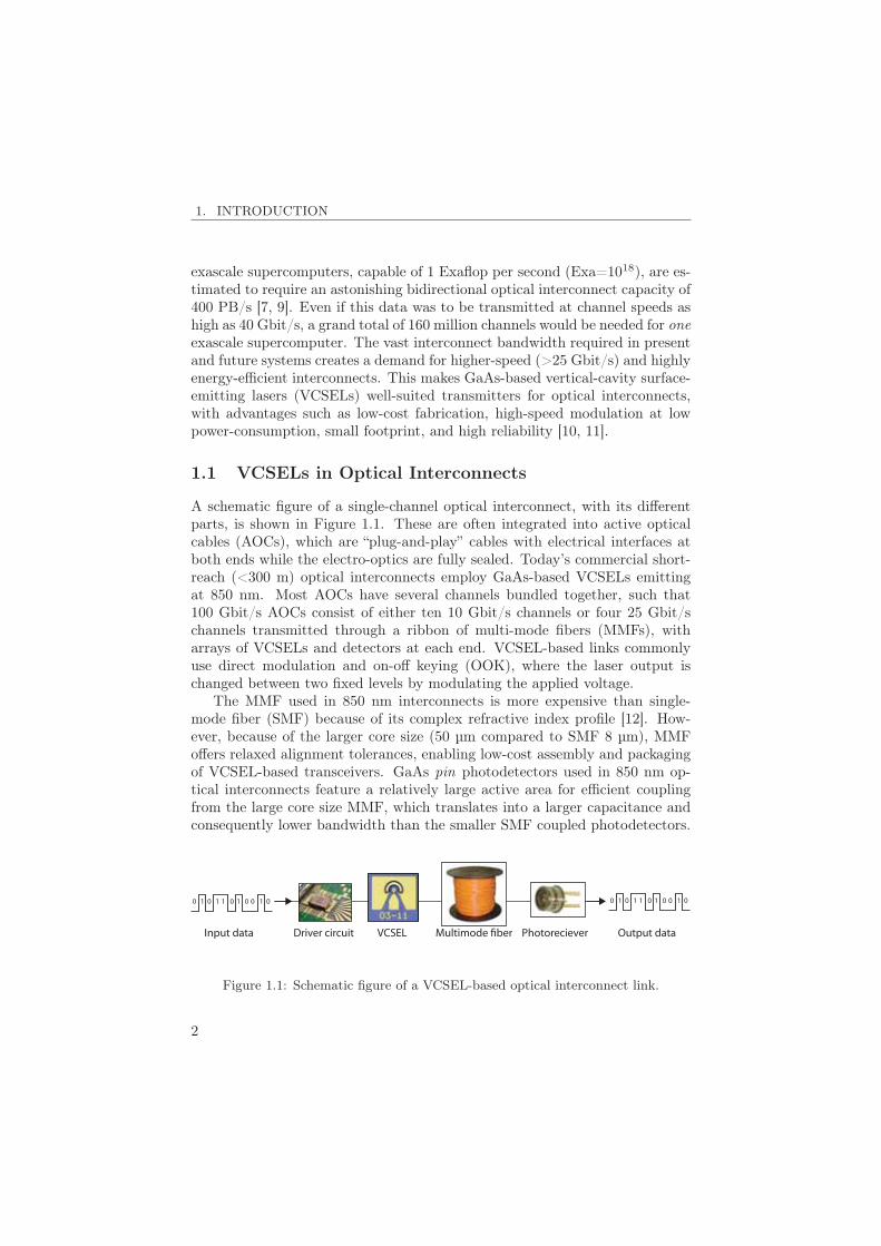
A schematic figure of a single-channel optical interconnect, with its differentparts, is shown in Figure 1.1. These are often integrated into active opticalcables (AOCs), which are “plug-and-play” cables with electrical interfaces atboth ends while the electro-optics are fully sealed. Today’s commercial short-reach (<300 m) optical interconnects employ GaAs-based VCSELs emittingat 850 nm. Most AOCs have several channels bundled together, such that100 Gbit/s AOCs consist of either ten 10 Gbit/s channels or four 25 Gbit/schannels transmitted through a ribbon of multi-mode fibers (MMFs), witharrays of VCSELs and detectors at each end. VCSEL-based links commonlyuse direct modulation and on-off keying (OOK), where the laser output ischanged between two fixed levels by modulating the applied voltage.
The MMF used in 850 nm interconnects is more expensive than single-mode fiber (SMF) because of its complex refractive index profile [12]. How-ever, because of the larger core size (50 μm compared to SMF 8 μm), MMFoffers relaxed alignment tolerances, enabling low-cost assembly and packagingof VCSEL-based transceivers. GaAs pin photodetectors used in 850 nm op-tical interconnects feature a relatively large active area for efficient couplingfrom the large core size MMF, which translates into a larger capacitance andconsequently lower bandwidth than the smaller SMF coupled photodetectors.
Multimode fiberDriver circuit PhotorecieverInput data
1 01 1 1 10 0 0 00
Output data
1 01 1 1 10 0 0 00
VCSEL
Figure 1.1: Schematic figure of a VCSEL-based optical interconnect link.
2
1.2. HIGH-SPEED VCSELS
This is equivalent to a trade-off between detector responsivity and bandwidth.The photodetector is one of the limiting factors for both reach and speed ofoptical interconnects, making the development of faster and more sensitivephotodetectors imperative.
Today, 850 nm GaAs-based VCSEL technology is used in 95% of all opticalnetworking applications <1000 m [13]. Depending on application, three stan-dardized data networking protocols dominate the 850 nm interconnect market;Ethernet (local area networks), Infiniband (high-performance computing, su-percomputers), and Fibre Channel (storage area networks). Even though thereare some differences, all work with 10-16 Gbit/s per channel over distances upto 300-550 m over OM4 MMF [14]. Higher-speed AOCs working at channelspeeds of ∼25 Gbit/s are expected in the very near future for distances up to100 m [15], and channel speeds up to 50 Gbit/s may be seen towards the end ofthis decade [16]. Parallel optical transceivers with arrays of VCSELs and pho-todetectors, each operating at 25 Gbit/s, will soon realize commercial opticalinterconnects with an aggregate capacity of 400 Gbit/s in each direction [15].
1.2 High-Speed VCSELs
Increasing the bandwidth and high-speed transmission properties of GaAs-based VCSELs at 850 nm has been an important research direction since theearly 1990’s [17]. Already in 1997, K. Lear et al. demonstrated VCSELs with21.5 GHz bandwidth, using an oxide-implanted 850 nm VCSEL [18]. The first20 Gbit/s operation of 850 nm VCSELs was presented by IBM in 2001 [19]. Ittook 7 years before 30 Gbit/s was demonstrated by Finisar in 2008, using anoxide-confined VCSEL [20]. However, only two years later, P. Westbergh et al.at Chalmers University of Technology demonstrated 850 nm VCSELs capableof 40 Gbit/s transmission [21]. These VCSELs also broke the old bandwidthrecord, achieving 23 GHz by optimization of the damping characteristics [22].Since then there has been an impressive development in VCSEL small-signalmodulation bandwidth, and especially high-speed data transmission. In 2013high-speed VCSELs from Chalmers with 28 GHz bandwidth enabled 57 Gbit/sat room temperature (RT), and 40 Gbit/s at 85°C [23, 24]. Using driver andreceiver circuits with electronic equalization, the same VCSELs could transmitat 71 Gbit/s at RT [25], and 50 Gbit/s up to 90°C [26]. This is the fastestVCSEL-based link to date without the use of forward error correction (FEC).The newest generation high-speed 850 nm VCSELs from Chalmers is presentedin Papers A and B. By strongly confining optical fields and carriers, a small-signal modulation bandwidth of 30 GHz was reached, which is currently therecord for conventional VCSELs. Current state-of-the-art bandwidths and
3
1. INTRODUCTION
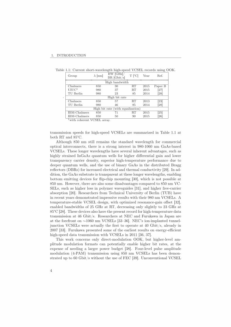
Table 1.1: Current short-wavelength high-speed VCSEL records using OOK.
.
Group λ [nm] BW [GHz]/BR [Gbit/s] T [°C] Year Ref.
High bandwidthChalmers 850 30 RT 2015 Paper BUIUC1 980 37 RT 2015 [27]TU Berlin 980 23 85 2014 [28]
High bit rateChalmers 850 57 RT 2013 [23]TU Berlin 980 46 85 2014 [28]
High bit rate (with equalization)IBM-Chalmers 850 71 RT 2015 [25]IBM-Chalmers 850 50 90 2015 [26]1with coherent VCSEL array.
transmission speeds for high-speed VCSELs are summarized in Table 1.1 atboth RT and 85°C.
Although 850 nm still remains the standard wavelength for commercialoptical interconnects, there is a strong interest in 980-1060 nm GaAs-basedVCSELs. These longer wavelengths have several inherent advantages, such ashighly strained InGaAs quantum wells for higher differential gain and lowertransparency carrier density, superior high-temperature performance due todeeper quantum wells, and the use of binary GaAs in the distributed Braggreflectors (DBRs) for increased electrical and thermal conductivity [29]. In ad-dition, the GaAs substrate is transparent at these longer wavelengths, enablingbottom emitting devices for flip-chip mounting [30], which is not possible at850 nm. However, there are also some disadvantages compared to 850 nm VC-SELs, such as higher loss in polymer waveguides [31], and higher free-carrierabsorption [20]. Researchers from Technical University of Berlin (TUB) havein recent years demonstrated impressive results with their 980 nm VCSELs. Atemperature-stable VCSEL design, with optimized resonance-gain offset [32],enabled bandwidths of 25 GHz at RT, decreasing only slightly to 23 GHz at85°C [28]. These devices also have the present record for high-temperature datatransmission at 46 Gbit/s. Researchers at NEC and Furukawa in Japan areat the forefront on ∼1060 nm VCSELs [33–36]. NEC’s ion-implanted tunnel-junction VCSELs were actually the first to operate at 40 Gbit/s, already in2007 [33]. Furukawa presented some of the earliest results on energy-efficienthigh-speed data transmission with VCSELs in 2011 [36, 37].
This work concerns only direct-modulation OOK, but higher-level am-plitude modulation formats can potentially enable higher bit rates, at theexpense of needing a larger power budget [38]. Four-level pulse amplitudemodulation (4-PAM) transmission using 850 nm VCSELs has been demon-strated up to 60 Gbit/s without the use of FEC [39]. Unconventional VCSEL
4
1.3. VCSELS FOR ENERGY-EFFICIENT DATA TRANSMISSION
structures with coupled cavities for multiple resonance peaks have recentlydemonstrated bandwidths exceeding 30 GHz. By tuning the photon-photonresonance peak, the modulation response can be lifted, enabling bandwidthsof up to 37 GHz [27]. Data transmission experiments at 40 Gbit/s have so farbeen presented using this type of devices [40]. Furthermore, there is ongoingresearch into utilizing other techniques than intensity modulation to transmitdata, such as polarization oscillation switching of spin-polarized VCSELs [41].
1.3 VCSELs for Energy-Efficient Data Transmission
Today’s widely deployed 10 Gbit/s optical interconnects typically consume25 pJ/bit [35]. The VCSEL itself typically consumes only a few percent of this(<1 pJ/bit), with the rest being used by the driver electronics and receiver. Tomake future high-speed interconnects for supercomputers and datacenters fea-sible, the link energy consumption must be dramatically reduced to ∼1 pJ/bit,also at higher channel speeds [7]. Even lower energies per bit may be needed asoptical links migrate closer to the processors, in for instance on-board and on-chip interconnects [1, 8]. The performance of state-of-the-art energy-efficientVCSEL links is stated in Table 1.2. Researchers at IBM have demonstratedenergy-efficient driver and receiver circuits in 32-nm SOI CMOS, increasing theVCSEL’s share of the total interconnect power consumption to 30-40% [42].This makes energy-efficient high-speed VCSELs an important research direc-tion. As seen in Table 1.2, the target performance of 1 pJ/bit was reached at25 Gbit/s, but already at 35 Gbit/s this almost tripled to 2.7 pJ/bit due tohigher driver and receiver power consumption, and increased VCSEL bias. Athigher bit rates, SiGe BiCMOS circuits with equalization have been used todemonstrate impressive transmission at 40-71 Gbit/s. However, they consumequite a lot of energy at ∼25 pJ/bit [25, 43–45]. A significant reduction in thepower consumption of high-bit-rate driver and receiver circuits will be neededto enable future VCSEL links at ≥40 Gbit/s.
Table 1.2: Energy efficiency of full VCSEL-based links. All results are for back-to-back transmission at RT using 850 nm VCSELs.
Group BR [Gbit/s] Link eff. VCSEL eff. (% of link) Year Ref.32-nm SOI CMOS
IBM-Sumitomo 25 1.0 pJ/bit 396 fJ/bit (40%) 2013 [42]IBM-Sumitomo 35 2.7 pJ/bit 800 fJ/bit (30%) 2013 [42]
130-nm SiGe BiCMOS (with equalization)IBM-Emcore 40 22.3 pJ/bit 653 fJ/bit (3%) 2012 [43]IBM-Finisar 56 23.7 pJ/bit 245 fJ/bit (1%) 2013 [44]IBM-Chalmers 64 26.3 pJ/bit 320 fJ/bit (1%) 2014 [45]
5
1. INTRODUCTION
Bit rate [Gbit/s]10 20 30 40 50 60 70
Ene
rgy
diss
ipat
ion
[fJ/b
it]
0
50
100
150
200
250
300
350
400
450
500
Others
ChalmersChalmers/IBMTUBNCUFurukawaNEC
850-980-1060 nm
Small-oxide aperture
Paper B
IBM (equalization)
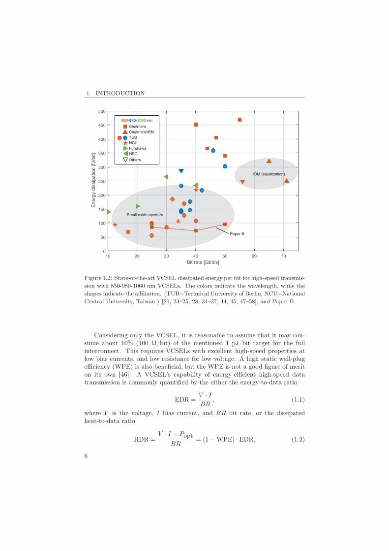
Figure 1.2: State-of-the-art VCSEL dissipated energy per bit for high-speed transmis-sion with 850-980-1060 nm VCSELs. The colors indicate the wavelength, while theshapes indicate the affiliation. (TUB=Technical University of Berlin, NCU=NationalCentral University, Taiwan.) [21, 23–25, 28, 34–37, 44, 45, 47–58], and Paper B.
Considering only the VCSEL, it is reasonable to assume that it may con-sume about 10% (100 fJ/bit) of the mentioned 1 pJ/bit target for the fullinterconnect. This requires VCSELs with excellent high-speed properties atlow bias currents, and low resistance for low voltage. A high static wall-plugefficiency (WPE) is also beneficial, but the WPE is not a good figure of meriton its own [46]. A VCSEL’s capability of energy-efficient high-speed datatransmission is commonly quantified by the either the energy-to-data ratio
EDR =V · IBR
, (1.1)
where V is the voltage, I bias current, and BR bit rate, or the dissipatedheat-to-data ratio
HDR =V · I − Popt
BR= (1− WPE) · EDR, (1.2)
6
1.3. VCSELS FOR ENERGY-EFFICIENT DATA TRANSMISSION
where Popt is the output optical power [48]. Considering only the VCSEL, theHDR is the more appropriate figure of merit, since the EDR does not takethe WPE into account, while it is obvious that a higher output power wouldbenefit the receiver energy efficiency. The EDR and HDR are given in fJ/bitin this work, but may also be stated in the equivalent unit of mW/(Tbit/s).
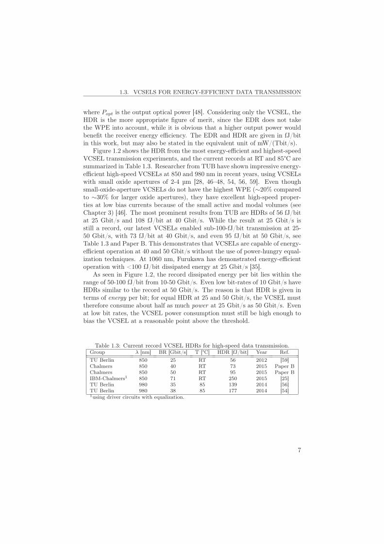
Figure 1.2 shows the HDR from the most energy-efficient and highest-speedVCSEL transmission experiments, and the current records at RT and 85°C aresummarized in Table 1.3. Researcher from TUB have shown impressive energy-efficient high-speed VCSELs at 850 and 980 nm in recent years, using VCSELswith small oxide apertures of 2-4 μm [28, 46–48, 54, 56, 59]. Even thoughsmall-oxide-aperture VCSELs do not have the highest WPE (∼20% comparedto ∼30% for larger oxide apertures), they have excellent high-speed proper-ties at low bias currents because of the small active and modal volumes (seeChapter 3) [46]. The most prominent results from TUB are HDRs of 56 fJ/bitat 25 Gbit/s and 108 fJ/bit at 40 Gbit/s. While the result at 25 Gbit/s isstill a record, our latest VCSELs enabled sub-100-fJ/bit transmission at 25-50 Gbit/s, with 73 fJ/bit at 40 Gbit/s, and even 95 fJ/bit at 50 Gbit/s, seeTable 1.3 and Paper B. This demonstrates that VCSELs are capable of energy-efficient operation at 40 and 50 Gbit/s without the use of power-hungry equal-ization techniques. At 1060 nm, Furukawa has demonstrated energy-efficientoperation with <100 fJ/bit dissipated energy at 25 Gbit/s [35].
As seen in Figure 1.2, the record dissipated energy per bit lies within therange of 50-100 fJ/bit from 10-50 Gbit/s. Even low bit-rates of 10 Gbit/s haveHDRs similar to the record at 50 Gbit/s. The reason is that HDR is given interms of energy per bit; for equal HDR at 25 and 50 Gbit/s, the VCSEL musttherefore consume about half as much power at 25 Gbit/s as 50 Gbit/s. Evenat low bit rates, the VCSEL power consumption must still be high enough tobias the VCSEL at a reasonable point above the threshold.
Table 1.3: Current record VCSEL HDRs for high-speed data transmission.Group λ [nm] BR [Gbit/s] T [°C] HDR [fJ/bit] Year Ref.TU Berlin 850 25 RT 56 2012 [59]Chalmers 850 40 RT 73 2015 Paper BChalmers 850 50 RT 95 2015 Paper BIBM-Chalmers1 850 71 RT 250 2015 [25]TU Berlin 980 35 85 139 2014 [56]TU Berlin 980 38 85 177 2014 [54]1using driver circuits with equalization.
7
1. INTRODUCTION
1.4 Longer-Reach Optical Interconnects
Long-reach optical interconnects for ∼500-2000 m currently employ InP-based1310 nm distributed feedback laser (DFB) and SMF [6]. Even though MMF ismore expensive per meter than SMF, the low-cost fabrication of VCSELs-basedtransceivers and energy-efficient direct modulation could still make VCSEL-based MMF links justifiable for long-reach optical interconnects by using850 nm VCSELs.
The launching and propagation of the VCSEL output signal through MMFis a complex process. First, the coupling of the VCSEL modes into the MMFis not a trivial problem. Depending on launch conditions such as angle, offsetfrom fiber center, and spot size, each VCSEL mode can excite several differ-ent fiber modes, referred to as mode groups. Second, there are three mainfiber-related effects that may limit the transmission distance over MMF; fiberloss, chromatic dispersion, and modal dispersion. The simplest, but oftennot limiting, is the absorption loss during propagation, which is 2.3 dB/kmat 850 nm for OM4 MMF. However, for commercial implementation of long-reach MMF links, it will be important to have a large received power in orderto have an adequate power budget for the link. The separation in wavelengthof the transverse modes emitted by the VCSEL cause a broadening of the sig-nal during propagation in the MMF by chromatic dispersion. In addition, thedifferent modes in the fiber have different propagation constants, giving rise tomodal dispersion. During modulation, the relative optical power in the VCSELmodes fluctuate by mode competition. This causes a random fluctuation inthe effects of modal dispersion and possible mode-selective losses and coupling,collectively referred to as mode-partition noise. In highly multimode VCSELlinks the mode-partition noise is reduced by the averaging over many modes,but lasers with a few modes can suffer greatly. Due to the absence of othermodes, single-mode lasers do not experience any significant mode-partitionnoise. The standard OM3 and OM4 MMFs have optimized graded-index pro-files in order to minimize the modal dispersion at 850 nm, making chromaticdispersion the dominating effect [60].
As a rule of thumb, at 10 Gbit/s, chromatic and modal fiber dispersionwill significantly distort the signal for transmission distances exceeding 300 mof OM4 MMF, causing inter-symbol-interference and bit errors [61]. At higherbit rates, the shorter bit slot makes the link even more sensitive to dispersioneffects, and the maximum transmission distance decreases even further. Thehighest transmission speed across 100 m of MMF is 43 Gbit/s (60 Gbit/s usingequalization) [23, 45]. In addition, commercial 850 nm AOCs are limited to100 m at 25 Gbit/s [62]. However, quasi-single-mode VCSELs with reducedspectral width, and thereby reduced effects of dispersion, may transmit at high
8
1.4. LONGER-REACH OPTICAL INTERCONNECTS
Bit rate [Gbit/s]10 20 30 40 50 60
Tran
smis
sion
dis
tanc
e [m
]
10
100
1000
10000
Chalmers
IBM
TUBNCU
Bell Labs
UIUC
MultimodeMode filterSmall oxidePhotonic crystal
AffiliationTechnique
Multimode, high speed
Quasi-single-mode, long reach
Paper C
Paper D
Paper E
Paper G
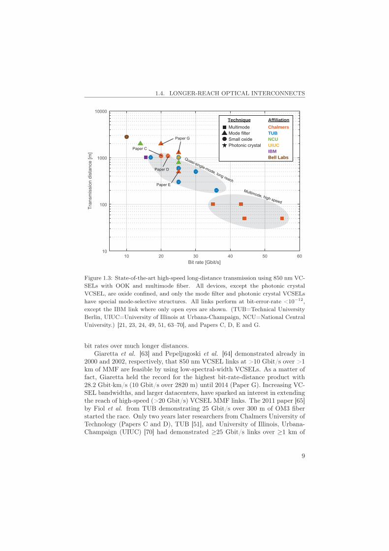
Figure 1.3: State-of-the-art high-speed long-distance transmission using 850 nm VC-SELs with OOK and multimode fiber. All devices, except the photonic crystalVCSEL, are oxide confined, and only the mode filter and photonic crystal VCSELshave special mode-selective structures. All links perform at bit-error-rate <10−12,except the IBM link where only open eyes are shown. (TUB=Technical UniversityBerlin, UIUC=University of Illinois at Urbana-Champaign, NCU=National CentralUniversity.) [21, 23, 24, 49, 51, 63–70], and Papers C, D, E and G.
bit rates over much longer distances.Giaretta et al. [63] and Pepeljugoski et al. [64] demonstrated already in
2000 and 2002, respectively, that 850 nm VCSEL links at >10 Gbit/s over >1km of MMF are feasible by using low-spectral-width VCSELs. As a matter offact, Giaretta held the record for the highest bit-rate-distance product with28.2 Gbit·km/s (10 Gbit/s over 2820 m) until 2014 (Paper G). Increasing VC-SEL bandwidths, and larger datacenters, have sparked an interest in extendingthe reach of high-speed (>20 Gbit/s) VCSEL MMF links. The 2011 paper [65]by Fiol et al. from TUB demonstrating 25 Gbit/s over 300 m of OM3 fiberstarted the race. Only two years later researchers from Chalmers University ofTechnology (Papers C and D), TUB [51], and University of Illinois, Urbana-Champaign (UIUC) [70] had demonstrated ≥25 Gbit/s links over ≥1 km of
9
1. INTRODUCTION
MMF, see Figure 1.3. This was possible by reducing the spectral width ofrecently developed high-speed VCSELs.
The most common approach is to use a small oxide aperture of ∼3 μm,as used in [51, 66, 68] and Papers C and D. The optical guiding can also bemodified by etching a photonic crystal in high-speed VCSELs as demonstratedby Tan et al. at UIUC [70]. Photonic crystal VCSELs can have excellentspectral properties and low resistance, but increased scattering loss reducesthe output power and efficiency. The technique of using a surface-relief modefilter to reduce the spectral width of VCSELs is applied in Papers E and F,enabling transmission at 25 Gbit/s over 500 m. A further development of themode-filter fabrication process improved this to 25 Gbit/s over 1300 m of OM4fiber and 20 Gbit/s over 2000 m, setting the still standing bit-rate-distance-product record of 40 Gbit·km/s for OOK 850 nm VCSEL links (Paper G). Themode-filter technique allows for a larger oxide aperture, with potentially lowerdifferential resistance, and higher output power to compensate for propagationloss in long-reach links. Shi et al. from National Central University, Taiwan(NCU), used a combination of mode filtering by Zn-diffusion and small oxiderelief (where the oxidized layer is completely removed for low capacitance)to achieve quasi-single-mode operation, enabling 14 Gbit/s over 2 km, and25 Gbit/s over 800 m [49, 67].
Higher-level amplitude modulation formats can potentially enable longer-reach transmission, but require a larger power budget [38], or complex circuitsfor FEC. 4-PAM has been demonstrated at 12.5 Gbit/s over 600 m of fiber[71], and 48.7 Gbit/s over 200 m using FEC [72]. The current record bit-rate-distance-product at 850 nm is 107.6 Gbit·km/s, and was achieved using discretemultitone modulation and FEC [73], while we hold the record for direct modu-lation OOK (Paper G). Future long-reach interconnects may also use VCSELsat 980 and 1060 nm, which have the advantage of significantly smaller loss andchromatic dispersion in the silica used in the optical fibers [74]. While the stan-dardized OM4 MMF is optimized for a low modal dispersion around 850 nm,fiber optimized for higher modal bandwidth, broader wavelength spans, andlonger wavelengths are currently being developed [75, 76]. Another competingtechnology is longer-wavelength VCSELs at 1310 or 1550 nm, where the use ofSMF avoids most of the effects of dispersion. Directly modulated InP-based1550 nm VCSELs have shown close-to error-free transmission at 40 Gbit/sover 1 km of SMF [77].
1.5 Multiplexing in Optical Interconnects
Besides higher single-channel speed, energy-efficiency, and longer-reach, thereis an additional need for a denser integration of transceivers and fibers. Su-percomputers are already approaching the point where there is no room for
10
1.5. MULTIPLEXING IN OPTICAL INTERCONNECTS
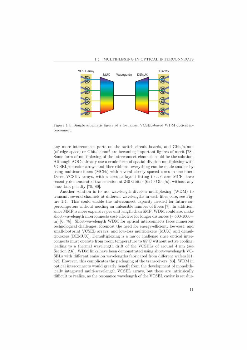
MUX DEMUXWaveguideVCSEL array PD array
Figure 1.4: Simple schematic figure of a 4-channel VCSEL-based WDM optical in-terconnect.
any more interconnect ports on the switch circuit boards, and Gbit/s/mm(of edge space) or Gbit/s/mm2 are becoming important figures of merit [78].Some form of multiplexing of the interconnect channels could be the solution.Although AOCs already use a crude form of spatial-division multiplexing withVCSEL/detector arrays and fiber ribbons, everything can be made smaller byusing multicore fibers (MCFs) with several closely spaced cores in one fiber.Dense VCSEL arrays, with a circular layout fitting to a 6-core MCF, haverecently demonstrated transmission at 240 Gbit/s (6x40 Gbit/s), without anycross-talk penalty [79, 80].
Another solution is to use wavelength-division multiplexing (WDM) totransmit several channels at different wavelengths in each fiber core, see Fig-ure 1.4. This could enable the interconnect capacity needed for future su-percomputers without needing an unfeasible number of fibers [7]. In addition,since MMF is more expensive per unit length than SMF, WDM could also makeshort-wavelength interconnects cost-effective for longer distances (∼500-1000+m) [6, 78]. Short-wavelength WDM for optical interconnects faces numeroustechnological challenges, foremost the need for energy-efficient, low-cost, andsmall-footprint VCSEL arrays, and low-loss multiplexers (MUX) and demul-tiplexers (DEMUX). Demultiplexing is a major challenge since optical inter-connects must operate from room temperature to 85°C without active cooling,leading to a thermal wavelength drift of the VCSELs of around 4 nm (seeSection 2.6). WDM links have been demonstrated using short-wavelength VC-SELs with different emission wavelengths fabricated from different wafers [81,82]. However, this complicates the packaging of the transceivers [83]. WDM inoptical interconnects would greatly benefit from the development of monolith-ically integrated multi-wavelength VCSEL arrays, but these are intrinsicallydifficult to realize, as the resonance wavelength of the VCSEL cavity is set dur-
11
1. INTRODUCTION
ing the epitaxial growth. This is further discussed in the second part of thisthesis that demonstrates multi-wavelength VCSEL arrays using high-contrastgratings (HCGs). Eventually, transmission over a ribbon of MCFs, with sev-eral wavelengths in each core, using high-speed VCSELs, and advanced driversand receivers, could enable 10’s of or even 100 Tbit/s capacity in a single AOC.
As of today, the only commercial short-wavelength WDM product on themarket is Cisco’s 40 Gbit/s BiDi transceivers that transmits counter-propaga-ting wavelengths at 832 and 918 nm in each fiber using VCSELs fabricatedfrom two different wafers [84]. Using a fiber pair, 2x20 Gbit/s is transmittedin each direction for a total bi-directional capacity of 40 Gbit/s. The broadcommercial breakthrough for short-wavelength WDM is yet to come, but thereis significant industrial interest in short-wavelength coarse WDM, and WDMin the 860-1100 nm range is currently being discussed in the IEEE 400 GigabitEthernet Task Force [85].
1.6 Scope and Outline of Thesis
The focus of this work has been on several important aspects of VCSELs forfuture optical interconnects. The first part concerns conventional 850 nm VC-SELs for longer-reach and energy-efficient data transmission at high data rates.Chapter 2 introduces the VCSEL fundamentals. It is followed by Chapter 3with a more detailed discussion on VCSEL dynamics and high-speed VCSELdesign. Chapter 4 describes the two different quasi-single-mode VCSEL ap-proaches used to enable longer-reach transmission; a small oxide aperture oran integrated mode filter. The VCSEL fabrication methods are described inChapter 5. The second part of the thesis presents the design, fabrication, andexperimental results for 980 nm multi-wavelength VCSEL arrays using HCGs.Chapter 6 describes the basics of HCGs and the design of HCG-VCSEL multi-wavelength arrays. The grating fabrication process is discussed in Chapter 7,followed by experimental results in Chapter 8. An outlook and future direc-tions, for both parts, are provided in Chapter 9. The results from the work onwhich this thesis is based are finally presented in the appended Papers A-H,which are summarized in Chapter 10.
12
Chapter 2
VCSEL Fundamentals
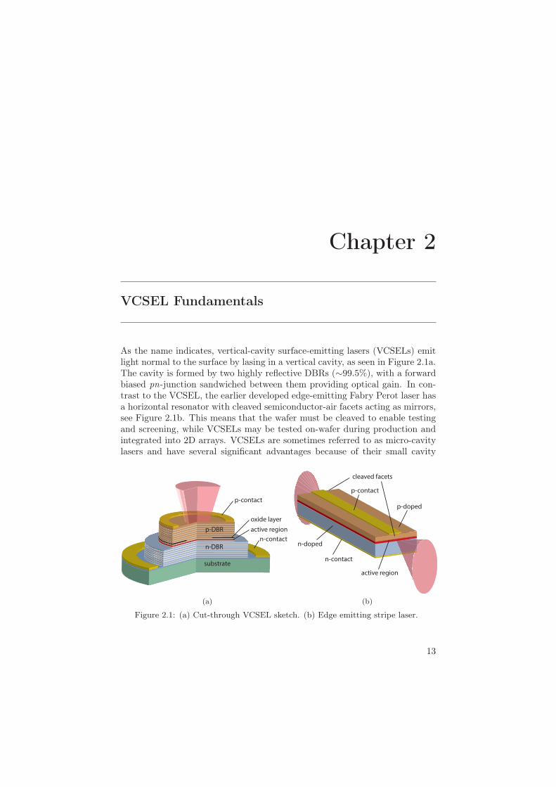
As the name indicates, vertical-cavity surface-emitting lasers (VCSELs) emitlight normal to the surface by lasing in a vertical cavity, as seen in Figure 2.1a.The cavity is formed by two highly reflective DBRs (∼99.5%), with a forwardbiased pn-junction sandwiched between them providing optical gain. In con-trast to the VCSEL, the earlier developed edge-emitting Fabry Perot laser hasa horizontal resonator with cleaved semiconductor-air facets acting as mirrors,see Figure 2.1b. This means that the wafer must be cleaved to enable testingand screening, while VCSELs may be tested on-wafer during production andintegrated into 2D arrays. VCSELs are sometimes referred to as micro-cavitylasers and have several significant advantages because of their small cavity
p-contact
oxide layer
n-contactp-DBR
n-DBR
active region
substrate
(a)
p-contact
active region
n-contact
cleaved facets
p-doped
n-doped
(b)
Figure 2.1: (a) Cut-through VCSEL sketch. (b) Edge emitting stripe laser.
13
2. VCSEL FUNDAMENTALS
size, such as low threshold currents and excellent high-speed properties at lowpower consumption.
2.1 History of VCSELs
The concept of a vertical-cavity semiconductor laser was first proposed in1977 by Professor K. Iga from Tokyo Institute of Technology, who two yearslater also demonstrated the first VCSEL, lasing under pulsed operation at77 K [86, 87]. The first VCSEL more resembled a “vertical edge emitter” witha relatively long cavity and metal-coated mirrors. The first reports on roomtemperature operation of VCSELs were published in 1989 [88, 89]. During the1990’s VCSEL research really took off and the first commercial VCSELs cameon the market in the middle of the decade. VCSEL-based short-reach fiber-optic links for data communication were introduced in 1996 [90]. Today 850 nmGaAs-based VCSEL technology is extensively utilized in short-reach opticalcommunication links, with 95% of all optical networking applications <1000 musing multimode fiber and 850 nm VCSELs [13]. The largest volume marketfor VCSELs is, however, in optical computer mice where 850 nm VCSELs areused to track movement on uniform surfaces with higher resolution and speedthan the earlier light-emitting diode (LED) optical mice [17]. In 2013, thetotal VCSEL production was around 100 million devices per year, with theprice of a computer-mouse 850 nm VCSEL approaching $0.10 [17]. VCSELproduction output is increasing, with larger wafer sizes being used to scale upproduction. In March 2014 IQE delivered the first 6" epitaxial VCSEL waferswhich can accommodate up to 300,000 VCSELs per wafer [91].
2.2 Cavity and Mirrors
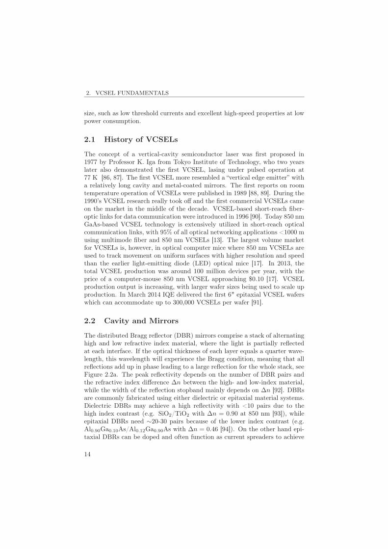
The distributed Bragg reflector (DBR) mirrors comprise a stack of alternatinghigh and low refractive index material, where the light is partially reflectedat each interface. If the optical thickness of each layer equals a quarter wave-length, this wavelength will experience the Bragg condition, meaning that allreflections add up in phase leading to a large reflection for the whole stack, seeFigure 2.2a. The peak reflectivity depends on the number of DBR pairs andthe refractive index difference Δn between the high- and low-index material,while the width of the reflection stopband mainly depends on Δn [92]. DBRsare commonly fabricated using either dielectric or epitaxial material systems.Dielectric DBRs may achieve a high reflectivity with <10 pairs due to thehigh index contrast (e.g. SiO2/TiO2 with Δn = 0.90 at 850 nm [93]), whileepitaxial DBRs need ∼20-30 pairs because of the lower index contrast (e.g.Al0.90Ga0.10As/Al0.12Ga0.90As with Δn = 0.46 [94]). On the other hand epi-taxial DBRs can be doped and often function as current spreaders to achieve
14
2.2. CAVITY AND MIRRORS
750 800 850 900 9500
0.2
0.4
0.6
0.8
1
Wavelength [nm]
Ref
lect
ivity
(a)
750 800 850 900 9500
0.2
0.4
0.6
0.8
1
Wavelength [nm]R
efle
ctiv
ity(b)
Figure 2.2: Calculated reflectivity spectra for (a) a VCSEL top DBR with 23 pairsof Al0.90Ga0.10As/Al0.12Ga0.88As and (b) a full VCSEL cavity. The single narrowlongitudinal resonance is seen at 845 nm.
a uniform injection of carriers into the active region. For the mirror where notransmission is required, a hybrid DBR may be used where the DBR is coveredwith gold or copper to increase reflectivity. The metal may also function asa heat sink and a contact for current injection. A completely different typeof mirror, based on a high-contrast grating (HCG), is used in the second partof this thesis (see Chapter 6). GaAs-based VCSEL designs commonly featureepitaxial DBRs in the mature AlGaAs material system.
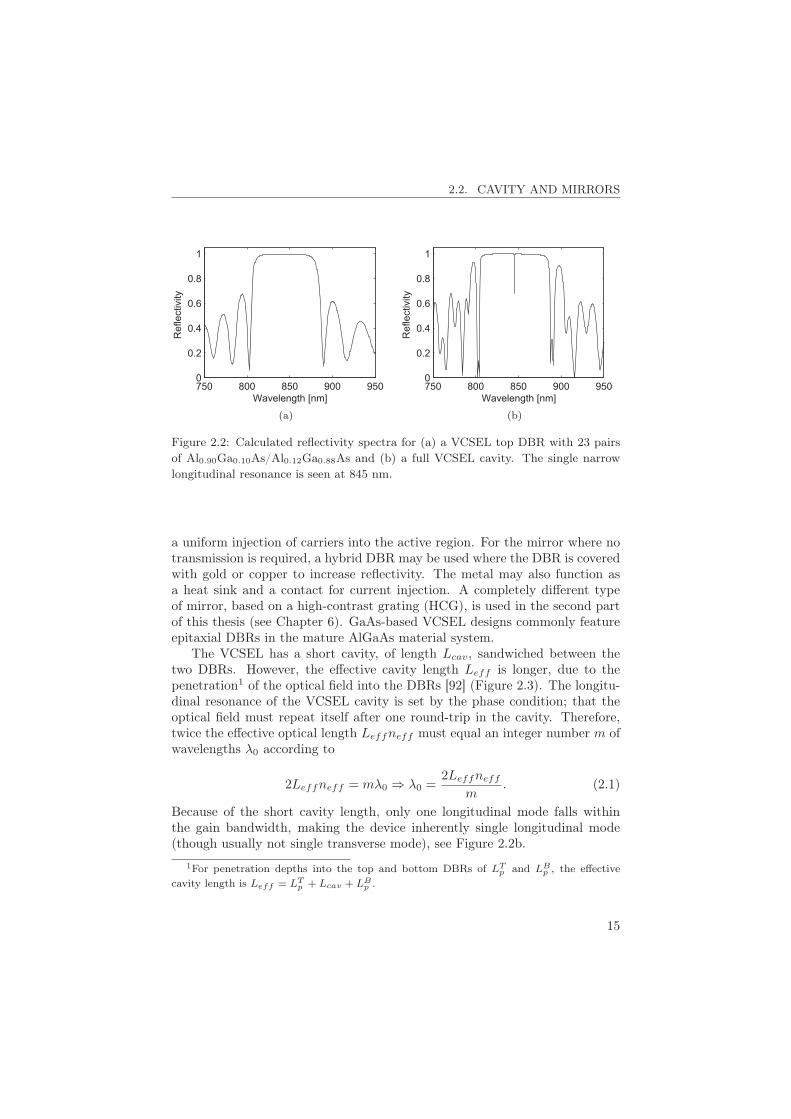
The VCSEL has a short cavity, of length Lcav, sandwiched between thetwo DBRs. However, the effective cavity length Leff is longer, due to thepenetration1 of the optical field into the DBRs [92] (Figure 2.3). The longitu-dinal resonance of the VCSEL cavity is set by the phase condition; that theoptical field must repeat itself after one round-trip in the cavity. Therefore,twice the effective optical length Leffneff must equal an integer number m ofwavelengths λ0 according to
2Leffneff = mλ0 ⇒ λ0 =2Leffneff
m. (2.1)
Because of the short cavity length, only one longitudinal mode falls withinthe gain bandwidth, making the device inherently single longitudinal mode(though usually not single transverse mode), see Figure 2.2b.
1For penetration depths into the top and bottom DBRs of LTp and LB
p , the effectivecavity length is Leff = LT
p + Lcav + LBp .
15
2. VCSEL FUNDAMENTALS
2.9 3 3.1 3.2 3.33
3.2
3.4
3.6
0 1 2 3 4 5 6 7
3
3.2
3.4
3.6
Depth [μm]
Ref
ract
ive
inde
xR
elat
ive
inte
nsity
98% oxide layers
top DBR bottom DBRQWs
QWsox.
Figure 2.3: Refractive index profile and simulated standing wave of the optical fieldinside a VCSEL cavity with a cavity length of 3/2-λ, and a double oxide layer abovethe active region. The inset shows the overlap of the standing wave with the quantumwells (QWs) and the nearest oxide layer (ox.). The substrate is to the right.
2.3 Active Region
The active region provides the optical gain. During lasing the modal gain mustbalance the optical losses according to
gth =1
Γ
(αi +
1
2Leffln
1
RTmRB
m
), (2.2)
where gth is the threshold gain, Γ the optical confinement factor representingthe fraction of the standing wave that overlaps with the active region, αi theinternal optical loss (due to free-carrier absorption and diffraction loss), andRT
m and RBm are the top and bottom mirror reflectivities. In semiconductor
lasers the optical gain by stimulated emission is achieved by injecting carri-ers into a forward biased pn-junction. Electrons and holes accumulate in theconduction and valence band respectively, which under high enough injectiongives rise to a population inversion and thereby optical gain. The first semi-conductor laser, demonstrated in 1962, had an active region consisting of aGaAs homojunction and could only operate in pulsed mode at 77 K becauseof the high band-to-band absorption [95]. Today the active region usuallyconsists of a pin-heterojunction with quantum wells (QWs) situated in thelower-bandgap intrinsic layer. The QWs trap the carriers, providing a high
16
2.4. OPTICAL AND ELECTRICAL CONFINEMENT
carrier density and a good spatial overlap between the electron and hole wavefunctions. Since the stimulated emission process is related to the optical fieldstrength, the QWs are placed at an antinode of the optical field to achieve ahigh gain, see Figure 2.3. State-of-the-art high-speed 850-1060 nm VCSELsuse strained InGaAs QWs which reduces the density of states, meaning thatfewer carriers are required to reach a certain gain (i.e. a larger differentialgain) [96]. GaAs-based VCSELs with highly strained InGaAs QWs have beendemonstrated up to ∼1300 nm [97], but beyond ∼1060-1100 nm the increasingQW strain leads to concerns regarding reliability.
2.4 Optical and Electrical Confinement
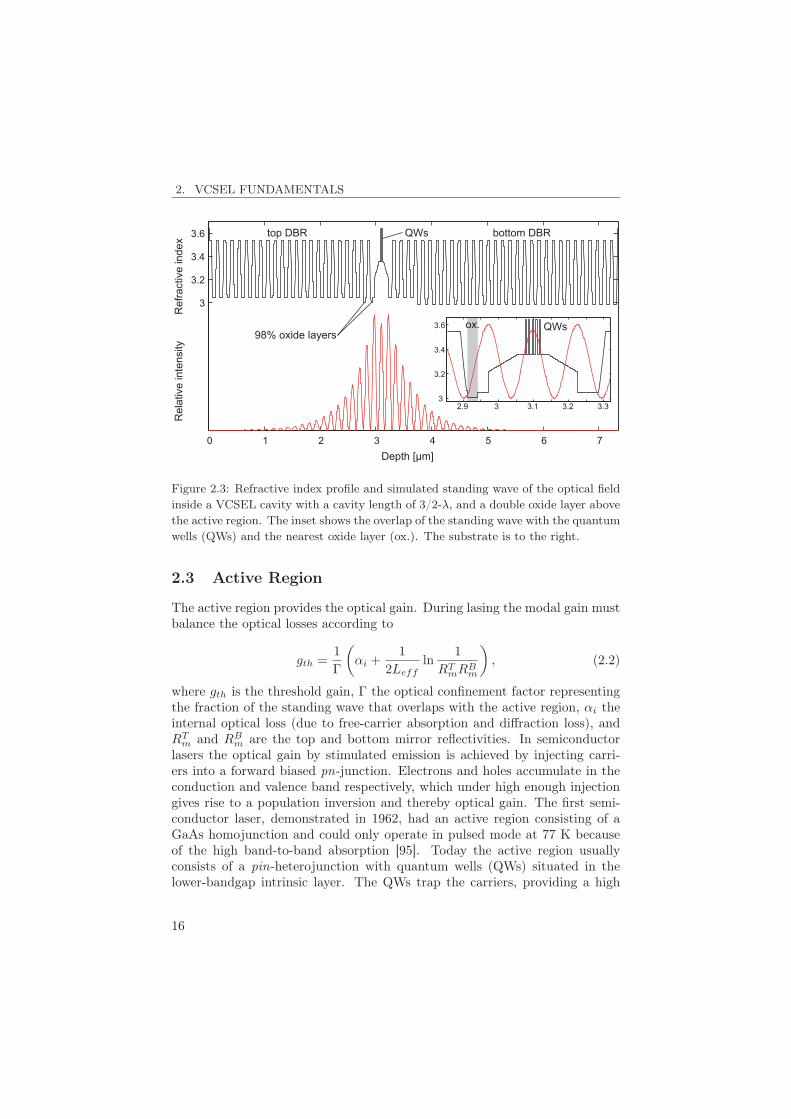
The DBRs confine the optical field in the longitudinal direction (Figure 2.3),but it must also be confined in the transverse direction. Furthermore, theelectrical current must be confined to pump only active material overlappingwith the lasing modes. In most VCSEL designs the electrical and optical con-finement originate from the same feature. The first VCSELs consisted of anetched air post mesa, see Figure 2.4a. The refractive index step from semicon-ductor to air provides index guiding, confining the optical field in the trans-verse direction. Although simple, this design has several issues such as highthermal resistance because of the surrounding air, large scattering losses fromrough sidewalls, and trouble with placing large enough top contacts for lowresistance while avoiding absorption losses from the metal. A further devel-opment is the buried heterostructure VCSEL seen in Figure 2.4b. By regrow-ing semi-insulating semiconductor material around the etched mesa, problemswith thermal resistance and losses are avoided, but the regrowth process ischallenging. The first commercial VCSELs instead used proton implantation,see Figure 2.4c. Protons are implanted deep into the top DBR, making thematerial insulating and forming the current aperture. The implanted materialdoes not form a direct index step for transverse optical confinement. How-ever, as the center of the waveguide heats up during operation, the refractiveindex increases, creating a refractive index gradient. This effect, referred toas thermal lensing, confines the optical field, but also leads to bias-dependentunstable modal properties. In addition, scattering of the protons during im-plantation, due to the large penetration depth into the top DBR, makes itdifficult to fabricate small-aperture devices.
Stable modal properties are obtained by including a built-in index step thatis sufficiently large compared to thermal lensing, gain guiding, and the plasmaeffect (decreasing refractive index with increased carrier concentration). Oneapproach is to use a selectively oxidized layer forming an oxide aperture, seeFigure 2.4d. A high Al-content layer (usually Al0.98Ga0.02As) is positioned in
17
2. VCSEL FUNDAMENTALS
air post
(a)
regrowth
(b)
proton implantation
(c)
oxide aperture
(d)
photonic crystal
(e)
tunnel junction
(f)
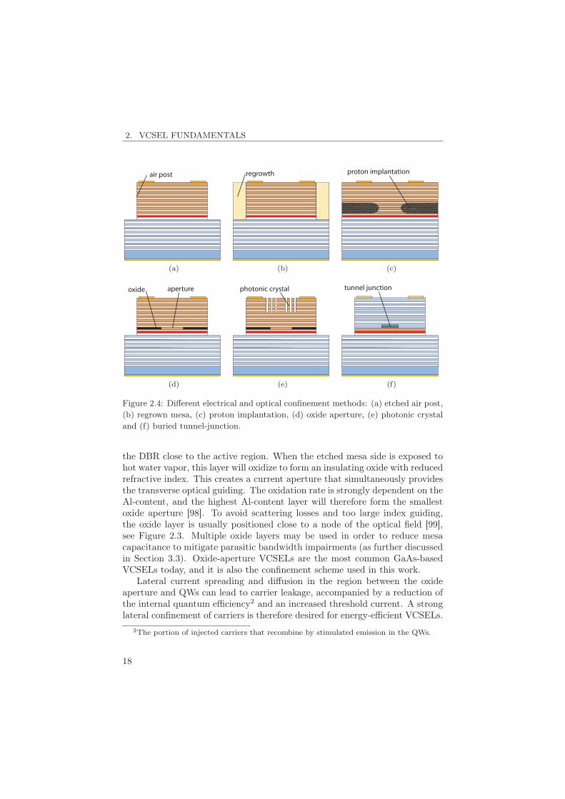
Figure 2.4: Different electrical and optical confinement methods: (a) etched air post,(b) regrown mesa, (c) proton implantation, (d) oxide aperture, (e) photonic crystaland (f) buried tunnel-junction.
the DBR close to the active region. When the etched mesa side is exposed tohot water vapor, this layer will oxidize to form an insulating oxide with reducedrefractive index. This creates a current aperture that simultaneously providesthe transverse optical guiding. The oxidation rate is strongly dependent on theAl-content, and the highest Al-content layer will therefore form the smallestoxide aperture [98]. To avoid scattering losses and too large index guiding,the oxide layer is usually positioned close to a node of the optical field [99],see Figure 2.3. Multiple oxide layers may be used in order to reduce mesacapacitance to mitigate parasitic bandwidth impairments (as further discussedin Section 3.3). Oxide-aperture VCSELs are the most common GaAs-basedVCSELs today, and it is also the confinement scheme used in this work.
Lateral current spreading and diffusion in the region between the oxideaperture and QWs can lead to carrier leakage, accompanied by a reduction ofthe internal quantum efficiency2 and an increased threshold current. A stronglateral confinement of carriers is therefore desired for energy-efficient VCSELs.
2The portion of injected carriers that recombine by stimulated emission in the QWs.
18
2.5. SPECTRAL CHARACTERISTICS
Since holes have lower mobility than electrons, the oxide aperture is typicallyplaced on the p-side to confine the slower holes, as this also prevents electronsfrom spreading outwards due to the requirement of charge neutrality. Currentspreading can be reduced by using un-doped intrinsic material between theoxide aperture and the QWs. This will not have a negative impact on thecarrier transport into the QWs if a properly designed short separate confine-ment heterostructure (SCH) is used [100]. Current spreading can be especiallytroublesome if there is any doped material between the oxide aperture and theQWs [24]. A strong confinement of the injected carriers is demonstrated in Pa-per A by positioning the oxide layers as close to the QWs as possible; in the firstfield minima of the standing wave on either side of the QWs. This approachhas previously demonstrated low current spreading and diffusion [101]. Theresulting high internal quantum efficiency and low threshold currents enabledhigh-speed transmission at record-high energy efficiencies (Paper B).
Decoupling of the electrical and optical confinement, in order to tailorthe optical properties of the VCSEL waveguide, can be achieved by etchinga 2D photonic crystal into the top DBR of an oxide-confined or proton im-planted VCSEL, see Figure 2.4e. In addition to increased design and processingcomplexity, the photonic crystal structure increases optical scattering losses,leading to lower output power and larger threshold current [17]. For long-wavelength InP-based VCSELs emitting at 1.3 and 1.55 μm, a buried tunneljunction is used for electrical and optical confinement since no high-qualityoxide exists in this material system, see Figure 2.4f [102]. This techniqueis not commonly used for electrical and optical confinement in GaAs-basedVCSELs because of the difficulty to design effective tunnel junctions, the com-plex regrowth process required, and the excellent properties of oxide-confinedVCSELs.
2.5 Spectral Characteristics
High-speed VCSELs usually have the shortest possible cavity lengths of 1/2-λor 3/2-λ, since this enhances the modulation bandwidth (Section 3.1). Becauseof the short cavity, VCSELs are inherently single longitudinal mode as onlyone longitudinal mode falls within the gain bandwidth. However, due to thelarge lateral dimensions (oxide aperture diameter ≥ 10λ), the VCSEL cavityoften supports several transverse modes. The spectral characteristics of theVCSEL can be analytically investigated using an effective index method [103],where the radial refractive index step is modeled as a parabolic refractive indexprofile according to
19
2. VCSEL FUNDAMENTALS
n2(r) =
{n2c(1− 2Δr2/a2) , r ≤ a
n2s = const , r > a
with Δ =n2c − n2
s
2n2c
≈ nc − ns
nc(2.3)
where r is the radial distance, a the radius of the oxide aperture, nc the coreeffective refractive index, and ns the effective index of the surrounding oxideregion. It should be noted that although Equation 2.3, strictly speaking, de-scribes a thermally guided VCSEL (e.g. an proton-implanted VCSEL), it maybe used to approximate an oxide-confined VCSEL [17, 103]. The advantage isthat this index profile yields analytical expressions for the spectral character-istics, which are useful for understanding the VCSEL modal properties. Bysolving the wave equation in this circular symmetric structure, the near-fieldintensity of the transverse modes becomes
Slp(r,Φ) ∝ |Elp(r,Φ)|2 ∝(2r2
ω20
)l [L(l)p−1
(2r2
ω20
)]2 { cos2(lΦ)
sin2(lΦ)
}exp
(−2r2
ω20
),
(2.4)where E is the optical field strength, ω0 the 1/e2 radius, Ll
p−1 the lth gener-alized Laguerre polynomial of order (p− 1), and Φ the azimuthal angle. Themodes are referred to as linearly polarized LPlp modes with intensity distri-bution as shown in Figure 2.5. For l > 0 the sin and cos factors representtwo different orthogonal states rotated 90◦/l with respect to each other. Fur-thermore, every mode has two orthogonal polarization states with the electricfield oscillating perpendicular to the propagation direction. Therefore, theGaussian-shaped fundamental mode LP01 has two polarization states, whilethe higher order modes with l > 0 have four states per LPlp mode. Thewavelength λlp of mode LPlp differs the fundamental longitudinal mode λ0 as
λlp = λ0
[1− (2p+ l − 1)
√Δ√2π
λ0
nca
], (2.5)
which shows that modes with the same mode index m = 2p + l − 1 have thesame emission wavelength [103]. From Equation 2.5 the mode spacing betweenadjacent mode index groups is
Δλ = |λm − λm+1| =√Δ√2π
λ20
nca∝
√Δ
Dox, (2.6)
where Dox = 2a is the oxide aperture diameter. The order and spacing ofthe modes agree well with the measured spectrum and near-field images in
20
2.5. SPECTRAL CHARACTERISTICS
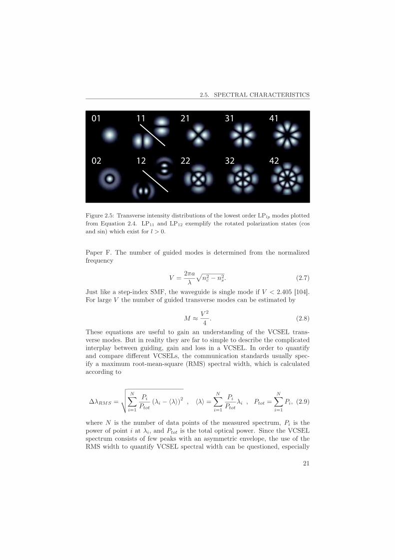
01 11 21 31 41
02 12 22 32 42
Figure 2.5: Transverse intensity distributions of the lowest order LPlp modes plottedfrom Equation 2.4. LP11 and LP12 exemplify the rotated polarization states (cosand sin) which exist for l > 0.
Paper F. The number of guided modes is determined from the normalizedfrequency
V =2πa
λ
√n2c − n2
s. (2.7)
Just like a step-index SMF, the waveguide is single mode if V < 2.405 [104].For large V the number of guided transverse modes can be estimated by
M ≈ V 2
4. (2.8)
These equations are useful to gain an understanding of the VCSEL trans-verse modes. But in reality they are far to simple to describe the complicatedinterplay between guiding, gain and loss in a VCSEL. In order to quantifyand compare different VCSELs, the communication standards usually spec-ify a maximum root-mean-square (RMS) spectral width, which is calculatedaccording to
ΔλRMS =
√√√√ N∑i=1
Pi
Ptot(λi − 〈λ〉)2 , 〈λ〉 =
N∑i=1
Pi
Ptotλi , Ptot =
N∑i=1
Pi, (2.9)
where N is the number of data points of the measured spectrum, Pi is thepower of point i at λi, and Ptot is the total optical power. Since the VCSELspectrum consists of few peaks with an asymmetric envelope, the use of theRMS width to quantify VCSEL spectral width can be questioned, especially
21
2. VCSEL FUNDAMENTALS
Wavelength
T1
cavity resonance
Gai
n
(a)
Wavelength
T2>T1
(b)
Wavelength
T3>T2
(c)
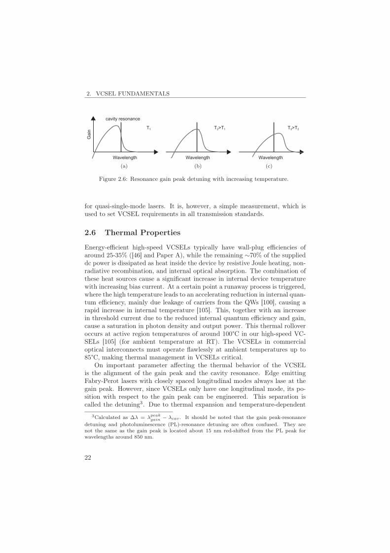
Figure 2.6: Resonance gain peak detuning with increasing temperature.
for quasi-single-mode lasers. It is, however, a simple measurement, which isused to set VCSEL requirements in all transmission standards.
2.6 Thermal Properties
Energy-efficient high-speed VCSELs typically have wall-plug efficiencies ofaround 25-35% ([46] and Paper A), while the remaining ∼70% of the supplieddc power is dissipated as heat inside the device by resistive Joule heating, non-radiative recombination, and internal optical absorption. The combination ofthese heat sources cause a significant increase in internal device temperaturewith increasing bias current. At a certain point a runaway process is triggered,where the high temperature leads to an accelerating reduction in internal quan-tum efficiency, mainly due leakage of carriers from the QWs [100], causing arapid increase in internal temperature [105]. This, together with an increasein threshold current due to the reduced internal quantum efficiency and gain,cause a saturation in photon density and output power. This thermal rolloveroccurs at active region temperatures of around 100°C in our high-speed VC-SELs [105] (for ambient temperature at RT). The VCSELs in commercialoptical interconnects must operate flawlessly at ambient temperatures up to85°C, making thermal management in VCSELs critical.
On important parameter affecting the thermal behavior of the VCSELis the alignment of the gain peak and the cavity resonance. Edge emittingFabry-Perot lasers with closely spaced longitudinal modes always lase at thegain peak. However, since VCSELs only have one longitudinal mode, its po-sition with respect to the gain peak can be engineered. This separation iscalled the detuning3. Due to thermal expansion and temperature-dependent
3Calculated as Δλ = λpeakgain − λcav . It should be noted that the gain peak-resonance
detuning and photoluminescence (PL)-resonance detuning are often confused. They arenot the same as the gain peak is located about 15 nm red-shifted from the PL peak forwavelengths around 850 nm.
22
2.6. THERMAL PROPERTIES
refractive index of the VCSEL cavity, the resonance wavelength is red-shiftedat 0.06 nm/°C with increasing temperature [106]. Meanwhile, the peak of theQW gain is red-shifted at 0.32-0.33 nm/°C due to bandgap shrinkage [107].As the gain peak is red-shifted faster, it will eventually outrun the cavity res-onance, leading to a reduced material gain and increasing threshold currentat high temperatures (Figure 2.6). This can be compensated by an initialnegative detuning. As the temperature is increased, the improved overlap ofthe gain and resonance compensates for the temperature-induced reductionof gain, and enables low thresholds even at high operating temperatures, asillustrated in Figure 2.6. A large negative detuning at RT can enable lasing atambient temperatures well above 100°C [108]. The impact of thermal effectson the VCSEL dynamics is discussed in Section 3.2.
23

24
Chapter 3
VCSEL Dynamics
For high-speed data transmission using direct modulation, the VCSEL outputpower should react rapidly to changes in bias current or voltage. However,an electron-hole pair takes some time before recombining (differential carrierlifetime), and the generated photon takes some time to leave the cavity (pho-ton lifetime1). By this simple example, it is clear that a VCSEL can not bemodulated infinitely fast. However, properly designed VCSELs can reach veryhigh modulation bandwidths at low bias currents, because of the strong in-teraction between the injected carriers and the photons in the small VCSELcavity. The complete dynamic behavior of a VCSEL is a complex interplay ofintrinsic, parasitic, and thermal properties, and is therefore challenging to ac-curately model [109]. This thesis work has been concerned with experimentalanalysis of high-speed VCSELs in Papers A to G. The first part of this chap-ter describes the small-signal intrinsic dynamics of the VCSEL. It is followedby a discussion of thermal and parasitic effects on the dynamics, combinedwith various implications for the design of high-speed VCSELs. Finally, themeasurement methods used for the small-signal modulation response measure-ments and data transmission experiments are presented.
3.1 Intrinsic Dynamics
The intrinsic dynamics of semiconductor lasers are governed by the resonantinteraction between the photons in the lasing modes and the injected electron-hole pairs in the active region. This can be described by the rate equations [92]:
1The photon is either transmitted through a mirror or lost by absorption or scattering.
25
3. VCSEL DYNAMICS
dN
dt=
ηiI
qVa− (
AN +BN2 + CN3)− vgGSm, (3.1)
dSm
dt= ΓvgGSm − Sm
τp+ ΓβBN2, (3.2)
where N is the excess carrier density in the active region, ηi the internalquantum efficiency, I the bias current, q the elementary charge, Va the activeregion volume2, A the Shockley-Read-Hall recombination coefficient3, B theradiative recombination coefficient, C the Auger recombination coefficient, vgis the group velocity, G the active region gain per unit length, Sm the photondensity in the cavity for mode m, Γ the longitudinal confinement factor, τpthe photon lifetime, and β the fraction of the spontaneous emission that goesinto the lasing mode. Since most VCSELs lase in multiple transverse modes, astrict rate equation analysis would involve one rate equation per mode. It has,however, been shown by both experiment and simulation that oxide-confinedVCSELs are well described by single-mode rate equations because of the tightoverlap of the modes due to the index guiding [110]. The subscript m inEquations 3.1 and 3.2 is therefore dropped, and the single-mode rate equationsare used. The compression of the gain at high photon densities, due non-lineareffects such as spectral hole burning and carrier heating [17], can be taken intoaccount by
G(N,S) =g(N)
1 + εS, (3.3)
where g is the uncompressed gain coefficient and ε the gain compression factor.Equation 3.1 and 3.2 are coupled differential equations and must in general besolved numerically. However, a small-signal analysis can be used to linearizethe equations in order to derive an analytical solution. A first-order Taylorexpansion can be made by setting
I = Ib + δI, (3.4)N = Nb + δN, (3.5)S = Sb + δS, (3.6)
G =gb
1 + εS+
g0δN
1 + εS− εgbδS
(1 + εS)2 , (3.7)
where index b indicates the bias point around which the linearization is done,and g0 = ∂g/∂N is the differential gain at the bias point. By inserting
2Equal to the oxide aperture area times total thickness of the QWs.3Defect-related non-radiative recombination.
26
3.1. INTRINSIC DYNAMICS
Equation 3.4 to 3.7 into the rate equations, neglecting the small spontaneousemission factor β, discarding higher order terms and time derivatives of con-stants, and eliminating ∂N , the differential equation representing a secondorder damped system is obtained as
d2
dt2δS + γ
d
dtδS + 4π2f2
r δS =ηiqVa
Γvgg0Sb
1 + εSbδI, (3.8)
where γ is the damping rate and fr the resonance frequency. By assuminga sinusoidal variation in the small deviations δI(t) = δI0e
j2πft and δS(t) =δS0e
j2πft, the time derivatives in Equation 3.8 can be replaced by j2πf . Fur-ther, the amplitude change in output power δP (t) = δP0e
j2πft is linearlyrelated to the photon density change δS in the cavity 4. This yields an approx-imate expression for the transfer function Hi(f) of the intrinsic small-signalmodulation response as
Hi(f) =δP0
δI0= const · f2
r
f2r − f2 + j f
2πγ. (3.9)
The modulation bandwidth f3dB is defined as the frequency where the responsehas dropped to half of its low-frequency value5. To obtain Equation 3.9, thefollowing approximate expressions for the characteristic parameters fr and γwere used [92]
fr ≈ 1
2π
√vgg0Sb
τp (1 + εSb), (3.10)
and
γ ≈ Kf2r + γ0, with K = 4π2
[τp +
ε
vgg0
], (3.11)
where γ0 is the damping offset and K is referred to as the K-factor. These twoequations govern the intrinsic response of the VCSEL. The resonance frequencyincreases with increasing photon density, leading to a larger bandwidth withincreasing bias current. However, the damping in turn increases even fasterwith photon density, and will eventually limit the modulation bandwidth sincefr ∝ √
Sb while γ ∝ Sb. The maximum intrinsic bandwidth of a VCSEL istherefore limited by the K-factor to [92]
4This assumes that the generated photon density is constant throughout the cavity. Thisis a good approximation for VCSELs, since the cavity round trip time of a photon τRT << τpdue to the high mirror reflectivity
5Equivalent to |Hi(f3dB)|2/|Hi(0)|2 = 1/2 (or -3 dB when plotted in dB scale).
27
3. VCSEL DYNAMICS
Frequency [GHz]0 10 20 30 40 50 60 70
Intri
nsic
mod
ulat
ion
resp
onse
[dB
]
-20
-15
-10
-5
0
5
10
S1<S2<S3<S4
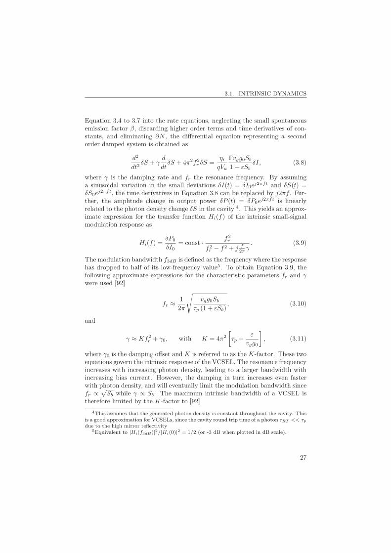
Figure 3.1: Damping-limited intrinsic modulation response for a VCSEL in Paper A,using K=0.14 ns and γ0=8.5 ns−1.
fmax3dB ≈ 2
√2π
K. (3.12)
The intrinsic modulation response for increasing photon densities is seen inFigure 3.1. The maximum modulation frequency is 63 GHz before the damp-ing limits the response. However, 63 GHz is far above the measured maximumbandwidth of 26 GHz for this particular device, because the VCSEL modula-tion response is reduced by thermal and parasitic effects, as discussed furtherin the following sections.
To reach a high resonance frequency, a large photon density is required. Inorder to quantify this, the D-factor is derived from Equation 3.10 as the rateat which the resonance frequency increases with increasing bias current as
fr = D ·√
I − Ith, with D =1
2π
√ηiΓvgqVa
· g0, (3.13)
where I is the bias current and Ith the threshold current. A high D-factorsignifies the ability to reach high resonance frequencies at low bias currents,and it is therefore an important figure of merit for energy-efficient VCSELs.The D-factor also shows that a small cavity volume6 enables VCSELs to reachhigh resonance frequencies at low bias currents. In Paper A we reduce themode volume by strongly confining the optical fields with the shortest possible
6The volume of the optical mode Vp is connected with the active region volume as Va =Γ · Vp.
28
3.2. THERMAL LIMITATIONS
cavity of 1/2-λ to facilitate a strong carrier-photon interaction. This yields∼20% increase in Γ compared to the next possible7 cavity length of 3/2-λ [24].
See [92] or [111] for a more detailed discussion on small-signal modulationdynamics and derivations. It should be noted that the expressions for the Dand K-factors in Paper A also include a transport factor χ, describing theeffects of carrier capture and escape from the QWs. However, for properlydesigned active regions χ is approximately equal to one [92].
3.2 Thermal Limitations
The VCSEL resonance frequency will keep increasing with√Ib − Ith until the
photon density saturates due to thermal effects (as described in Section 2.6).By setting γ=0 in Equation 3.9, the thermally limited modulation bandwidthcan be estimated as
f thermal3dB =
√1 +
√2 · fr ≈ 1.55 · fr. (3.14)
A high D-factor is therefore beneficial in order to reach a high resonance fre-quency before thermal saturation kicks in. Since the resonance frequency sat-urates at high temperatures, the D-factor is evaluated at low currents, whereself-heating effects are negligible and Equation 3.13 is valid. At higher ambi-ent temperatures, the D-factor is reduced by the decrease in ηi due to carrierleakage from the QWs, and the reduced g0 due to the higher carrier concen-tration needed to reach the threshold material gain at elevated temperatures.In contrast, the K-factor is relatively insensitive to changes in temperature([112] and Paper A). The reason is that the free-carrier absorption increasesat high temperatures, because of increased phonon scattering rates leading toreduced carrier relaxation times [113]. Meanwhile, g0 is reduced. These twoeffects cancel out, leading to a temperature-stable K-factor.
The gain-resonance detuning discussed, in Section 2.6, has an importanteffect on the thermal high-speed performance, as it influences both Ith andg0, which is considerably higher on the short-wavelength side of the gainpeak [32, 114]. The detuning can be investigated experimentally by mea-suring Ith as a function of temperature, and finding the temperature for theminimum threshold with a quadratic fit. At this temperature, the gain peakand resonance are aligned and the detuning is zero. Our high-speed VC-SELs typically have minimum Ith at around 0°C, meaning that the detuningis positive above this temperature ([111] and Paper A). This indicates that
7A cavity length of for instance λ is also possible. But the standing wave will not havea node in the middle of the cavity where the QWs are preferably positioned.
29
3. VCSEL DYNAMICS
we have a positive detuning of around 6 nm at RT8, growing larger as thetemperature increases. A steadily increasing positive detuning is disadvan-tageous for the high-temperature static performance as the VCSEL must bepumped harder to compensate for the lower gain. However, it is beneficialfor the dynamic performance at RT due to the higher g0. By using a differ-ent approach with a large negative detuning of ∼15 nm, researchers at TUBhave demonstrated impressive results for temperature-stable high-speed 980nm VCSELs [28, 54, 56, 108]. The negative detuning facilitates temperature-insensitive threshold currents and slope efficiencies, enabling data transmissionat 38 Gbit/s from RT to 95°C with unchanged bias conditions [32]. However,the temperature stability comes at the price of worse performance at low andmiddle temperatures, for instance a lower g0 from RT to ∼70°C, compared to0 nm detuning at RT.
Except for the detuning, there are basically two viable strategies to miti-gate detrimental thermal effects; either prevent heating in the first place, orconduct away the generated heat by appropriate heat sinking. Carrier leakagefrom the QWs could potentially be reduced by an electron blocking layer [115],but this may have adverse effects on the carrier transport and dynamic per-formance. To simultaneously reduce Joule heating and optical absorption inthe DBRs is challenging, since the first requires higher doping levels and thelatter lower. A good compromise can be obtained by using modulation dopingschemes, with higher doping levels at the nodes of the standing optical field.In a first approximation, this can be achieved by minimizing the resistance-loss product [24, 116]. Another approach is to use intra-cavity contacts toavoid injection of carriers through the resistive DBRs, where most of the Jouleheating and free-carrier absorption occurs [33, 53]. However, the long lateraldistance the carriers must travel may lead to uneven carrier injection withcurrent crowding at the oxide aperture edges. This is especially harmful forquasi-single-mode VCSELs, as the higher order modes will experience a largermodal gain due to a better spatial overlap with the carriers (Chapter 4). Anefficient heat-extraction from the active region can be achieved by using ma-terials with high thermal conductivity in the design. VCSELs emitting at850 nm may use binary AlAs in the bottom mirror due to its higher thermalconductivity than for instance Al0.90Ga0.10As [117]. At longer wavelengths,where also GaAs is transparent, a fully binary GaAs/AlAs bottom DBR maybe used. Papers A to G use AlAs/Al0.12Ga0.88As in the bottom DBR for goodthermal conductivity. Heat-sinking may be improved by electroplating themesa sidewalls with metal [118], or by removing the substrate and electroplat-ing a metal substrate [119]. However, introducing large metal areas generallyleads to larger capacitances, increasing the parasitic limitations.
8Assuming the gain peak is red-shifted at 0.32 nm/°C [107], and the cavity resonancewith 0.06 nm/°C [106].
30
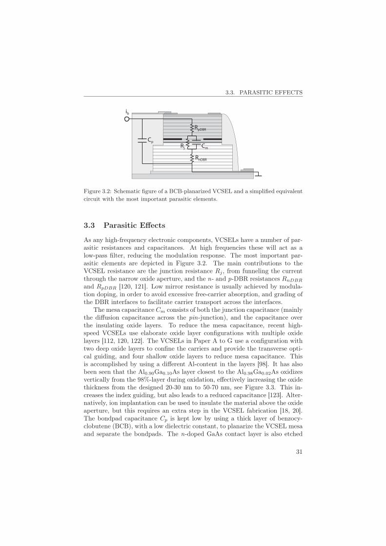
3.3. PARASITIC EFFECTS
CpRj Cm
RpDBR
RnDBR
ib
Figure 3.2: Schematic figure of a BCB-planarized VCSEL and a simplified equivalentcircuit with the most important parasitic elements.
3.3 Parasitic Effects
As any high-frequency electronic components, VCSELs have a number of par-asitic resistances and capacitances. At high frequencies these will act as alow-pass filter, reducing the modulation response. The most important par-asitic elements are depicted in Figure 3.2. The main contributions to theVCSEL resistance are the junction resistance Rj , from funneling the currentthrough the narrow oxide aperture, and the n- and p-DBR resistances RnDBR
and RpDBR [120, 121]. Low mirror resistance is usually achieved by modula-tion doping, in order to avoid excessive free-carrier absorption, and grading ofthe DBR interfaces to facilitate carrier transport across the interfaces.
The mesa capacitance Cm consists of both the junction capacitance (mainlythe diffusion capacitance across the pin-junction), and the capacitance overthe insulating oxide layers. To reduce the mesa capacitance, recent high-speed VCSELs use elaborate oxide layer configurations with multiple oxidelayers [112, 120, 122]. The VCSELs in Paper A to G use a configuration withtwo deep oxide layers to confine the carriers and provide the transverse opti-cal guiding, and four shallow oxide layers to reduce mesa capacitance. Thisis accomplished by using a different Al-content in the layers [98]. It has alsobeen seen that the Al0.90Ga0.10As layer closest to the Al0.98Ga0.02As oxidizesvertically from the 98%-layer during oxidation, effectively increasing the oxidethickness from the designed 20-30 nm to 50-70 nm, see Figure 3.3. This in-creases the index guiding, but also leads to a reduced capacitance [123]. Alter-natively, ion implantation can be used to insulate the material above the oxideaperture, but this requires an extra step in the VCSEL fabrication [18, 20].The bondpad capacitance Cp is kept low by using a thick layer of benzocy-clobutene (BCB), with a low dielectric constant, to planarize the VCSEL mesaand separate the bondpads. The n-doped GaAs contact layer is also etched
31
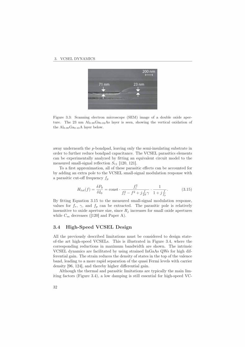
3. VCSEL DYNAMICS
200 nm
71 nm 23 nm
Figure 3.3: Scanning electron microscope (SEM) image of a double oxide aper-ture. The 23 nm Al0.98Ga0.02As layer is seen, showing the vertical oxidation ofthe Al0.90Ga0.10A layer below.
away underneath the p-bondpad, leaving only the semi-insulating substrate inorder to further reduce bondpad capacitance. The VCSEL parasitics elementscan be experimentally analyzed by fitting an equivalent circuit model to themeasured small-signal reflection S11 [120, 121].
To a first approximation, all of these parasitic effects can be accounted forby adding an extra pole to the VCSEL small-signal modulation response witha parasitic cut-off frequency fp
Htot(f) =δP0
δI0= const · f2
r
f2r − f2 + j f
2πγ· 1
1 + j ffp
. (3.15)
By fitting Equation 3.15 to the measured small-signal modulation response,values for fr, γ, and fp can be extracted. The parasitic pole is relativelyinsensitive to oxide aperture size, since Rj increases for small oxide apertureswhile Cm decreases ([120] and Paper A).
3.4 High-Speed VCSEL Design
All the previously described limitations must be considered to design state-of-the art high-speed VCSELs. This is illustrated in Figure 3.4, where thecorresponding reductions in maximum bandwidth are shown. The intrinsicVCSEL dynamics are facilitated by using strained InGaAs QWs for high dif-ferential gain. The strain reduces the density of states in the top of the valenceband, leading to a more rapid separation of the quasi Fermi levels with carrierdensity [96, 124], and thereby higher differential gain.
Although the thermal and parasitic limitations are typically the main lim-iting factors (Figure 3.4), a low damping is still essential for high-speed VC-
32
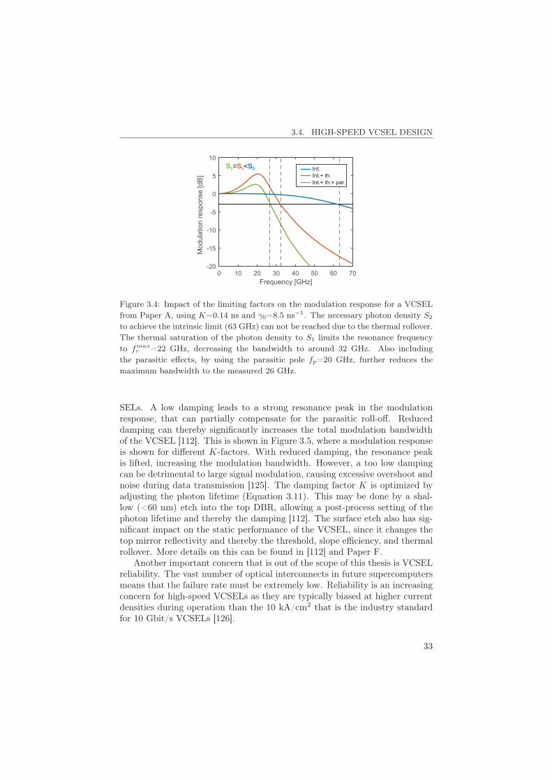
3.4. HIGH-SPEED VCSEL DESIGN
Frequency [GHz]0 10 20 30 40 50 60 70
Mod
ulat
ion
resp
onse
[dB
]
-20
-15
-10
-5
0
5
10S1=S1<S2 Int.
Int.+ th.Int.+ th.+ par.
Figure 3.4: Impact of the limiting factors on the modulation response for a VCSELfrom Paper A, using K=0.14 ns and γ0=8.5 ns−1. The necessary photon density S2
to achieve the intrinsic limit (63 GHz) can not be reached due to the thermal rollover.The thermal saturation of the photon density to S1 limits the resonance frequencyto fmax
r =22 GHz, decreasing the bandwidth to around 32 GHz. Also includingthe parasitic effects, by using the parasitic pole fp=20 GHz, further reduces themaximum bandwidth to the measured 26 GHz.
SELs. A low damping leads to a strong resonance peak in the modulationresponse, that can partially compensate for the parasitic roll-off. Reduceddamping can thereby significantly increases the total modulation bandwidthof the VCSEL [112]. This is shown in Figure 3.5, where a modulation responseis shown for different K-factors. With reduced damping, the resonance peakis lifted, increasing the modulation bandwidth. However, a too low dampingcan be detrimental to large signal modulation, causing excessive overshoot andnoise during data transmission [125]. The damping factor K is optimized byadjusting the photon lifetime (Equation 3.11). This may be done by a shal-low (<60 nm) etch into the top DBR, allowing a post-process setting of thephoton lifetime and thereby the damping [112]. The surface etch also has sig-nificant impact on the static performance of the VCSEL, since it changes thetop mirror reflectivity and thereby the threshold, slope efficiency, and thermalrollover. More details on this can be found in [112] and Paper F.
Another important concern that is out of the scope of this thesis is VCSELreliability. The vast number of optical interconnects in future supercomputersmeans that the failure rate must be extremely low. Reliability is an increasingconcern for high-speed VCSELs as they are typically biased at higher currentdensities during operation than the 10 kA/cm2 that is the industry standardfor 10 Gbit/s VCSELs [126].
33
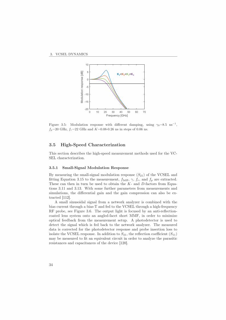
3. VCSEL DYNAMICS
Frequency [GHz]0 10 20 30 40 50 60 70
Mod
ulat
ion
resp
onse
[dB
]
-20
-15
-10
-5
0
5
10
K1<K2<K3<K4
Figure 3.5: Modulation response with different damping, using γ0=8.5 ns−1,fp=20 GHz, fr=22 GHz and K=0.08-0.26 ns in steps of 0.06 ns.
3.5 High-Speed Characterization
This section describes the high-speed measurement methods used for the VC-SEL characterization.
3.5.1 Small-Signal Modulation Response
By measuring the small-signal modulation response (S21) of the VCSEL andfitting Equation 3.15 to the measurement, f3dB , γ, fr, and fp are extracted.These can then in turn be used to obtain the K- and D-factors from Equa-tions 3.11 and 3.13. With some further parameters from measurements andsimulations, the differential gain and the gain compression can also be ex-tracted [112].
A small sinusoidal signal from a network analyzer is combined with thebias current through a bias-T and fed to the VCSEL through a high-frequencyRF probe, see Figure 3.6. The output light is focused by an anti-reflection-coated lens system onto an angled-facet short MMF, in order to minimizeoptical feedback from the measurement setup. A photodetector is used todetect the signal which is fed back to the network analyzer. The measureddata is corrected for the photodetector response and probe insertion loss toisolate the VCSEL response. In addition to S21, the reflection coefficient (S11)may be measured to fit an equivalent circuit in order to analyze the parasiticresistances and capacitances of the device [120].
34
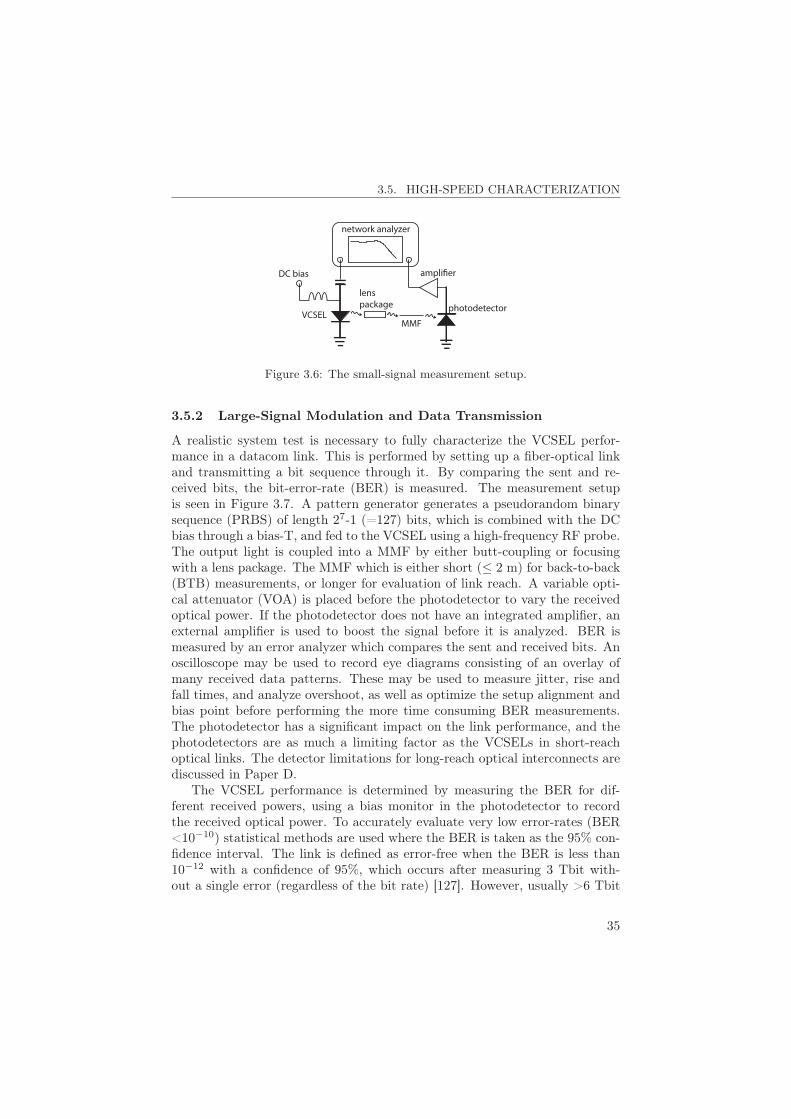
3.5. HIGH-SPEED CHARACTERIZATION
network analyzer
MMF
amplifier
VCSEL
DC bias
photodetector
lens package
Figure 3.6: The small-signal measurement setup.
3.5.2 Large-Signal Modulation and Data Transmission
A realistic system test is necessary to fully characterize the VCSEL perfor-mance in a datacom link. This is performed by setting up a fiber-optical linkand transmitting a bit sequence through it. By comparing the sent and re-ceived bits, the bit-error-rate (BER) is measured. The measurement setupis seen in Figure 3.7. A pattern generator generates a pseudorandom binarysequence (PRBS) of length 27-1 (=127) bits, which is combined with the DCbias through a bias-T, and fed to the VCSEL using a high-frequency RF probe.The output light is coupled into a MMF by either butt-coupling or focusingwith a lens package. The MMF which is either short (≤ 2 m) for back-to-back(BTB) measurements, or longer for evaluation of link reach. A variable opti-cal attenuator (VOA) is placed before the photodetector to vary the receivedoptical power. If the photodetector does not have an integrated amplifier, anexternal amplifier is used to boost the signal before it is analyzed. BER ismeasured by an error analyzer which compares the sent and received bits. Anoscilloscope may be used to record eye diagrams consisting of an overlay ofmany received data patterns. These may be used to measure jitter, rise andfall times, and analyze overshoot, as well as optimize the setup alignment andbias point before performing the more time consuming BER measurements.The photodetector has a significant impact on the link performance, and thephotodetectors are as much a limiting factor as the VCSELs in short-reachoptical links. The detector limitations for long-reach optical interconnects arediscussed in Paper D.
The VCSEL performance is determined by measuring the BER for dif-ferent received powers, using a bias monitor in the photodetector to recordthe received optical power. To accurately evaluate very low error-rates (BER<10−10) statistical methods are used where the BER is taken as the 95% con-fidence interval. The link is defined as error-free when the BER is less than10−12 with a confidence of 95%, which occurs after measuring 3 Tbit with-out a single error (regardless of the bit rate) [127]. However, usually >6 Tbit
35
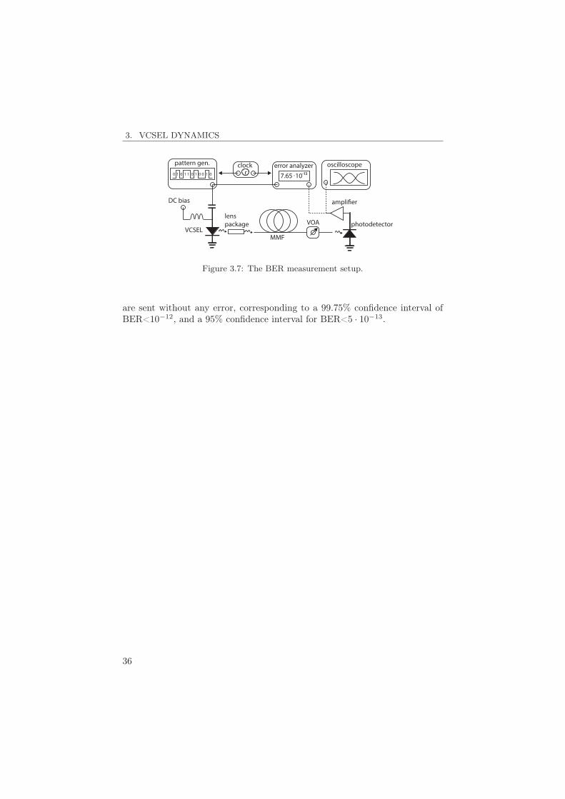
3. VCSEL DYNAMICS
pattern gen. error analyzer10 0 0 0 001 1 1 1
MMF
amplifier
VCSEL
oscilloscopeclock
DC bias
VOA photodetector
7.65 10-13
lens package
Figure 3.7: The BER measurement setup.
are sent without any error, corresponding to a 99.75% confidence interval ofBER<10−12, and a 95% confidence interval for BER<5 · 10−13.
36
Chapter 4
Quasi-Single Mode VCSELs
For a VCSEL to be referred to as single mode, a side-mode suppression ra-tio (SMSR) larger than 30 dB is typically required. If nothing else is speci-fied, single mode usually refers to a VCSEL lasing in the fundamental LP01
mode, which has two different polarizations. Single-polarization emission canbe achieved by introducing some anisotropy in the cavity, for instance by usinggratings [128]. Single-mode VCSELs have been extensively researched sincethe beginning of VCSEL development. They are essential for long-wavelength(1.3 and 1.55 μm) communication VCSELs and many sensing applicationssuch as gas sensing [129]. However, most applications poise complicated de-mands on the VCSEL, leading to a trade-off between output power, high-speedproperties, and spectral characteristics. As previously discussed in Figure 1.3,almost all of the reported highest bit-rate-distance product 850 nm VCSELlinks today use single-mode or quasi-single-mode VCSELs. The term quasi-single-mode does not have a clear definition, other than being a VCSEL thatis almost single mode. The term is used in this thesis to refer to VCSELs withan SMSR of ∼15-20 dB.
There are several designs aimed at achieving single-mode emission or low-spectral width of 850 nm GaAs-based VCSELs. In general there are twodifferent approaches; an inherently single-mode waveguide, or a mode selec-tive loss. The former includes photonic crystal VCSELs and basically anydevice with a narrow enough transverse aperture and sufficiently small indexstep [130]. Mode selective losses can be implemented by for instance metalapertures, extended cavities, and shallow surface reliefs [131–133]. There arealso more complex VCSEL designs with non-epitaxial structures, such as usinga curved external mirror which has achieved 15 mW of single-mode power [134].This thesis concerns two of the most promising approaches to simultaneously
37
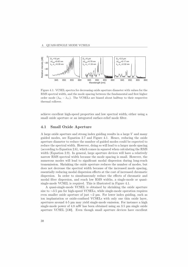
4. QUASI-SINGLE MODE VCSELS
Dox=10 μm
RMS=0.62 nm
01 11=0.35 nm
845 850 855 860
0
Rel
ativ
e in
tens
ity [d
B]
845 850 855 860Wavelength [nm]
Dox=5 μm
RMS=0.79 nm
01 11=1.33 nm
845 850 855 860
Dox=3.5 μm
RMS=0.17 nm
01 11=2.32 nm
Figure 4.1: VCSEL spectra for decreasing oxide aperture diameter with values for theRMS spectral width, and the mode spacing between the fundamental and first higherorder mode (λ01 − λ11). The VCSELs are biased about halfway to their respectivethermal rollover.
achieve excellent high-speed properties and low spectral width; either using asmall oxide aperture or an integrated surface-relief mode filter.
4.1 Small Oxide Aperture
A large oxide aperture and strong index guiding results in a large V and manyguided modes, see Equation 2.7 and Figure 4.1. Hence, reducing the oxideaperture diameter to reduce the number of guided modes could be expected toreduce the spectral width. However, doing so will lead to a larger mode spacing(according to Equation 2.6), which comes in squared when calculating the RMSwidth (Equation 2.9). In general, large aperture devices will have a relativelynarrow RMS spectral width because the mode spacing is small. However, thenumerous modes will lead to significant modal dispersion during long-reachtransmission. Shrinking the oxide aperture reduces the number of modes, butdoes not decrease the spectral width because of the increased mode spacing,essentially reducing modal dispersion effects at the cost of increased chromaticdispersion. In order to simultaneously reduce the effects of chromatic andmodal fiber dispersion, and reach low RMS widths, a single-mode or quasi-single-mode VCSEL is required. This is illustrated in Figure 4.1.
A quasi-single-mode VCSEL is obtained by shrinking the oxide aperturesize to ∼3.5 μm for high-speed VCSELs, while single-mode operation requireseven smaller oxide aperture of just ∼2 μm. For lower index guiding, such asion implantation or oxide-confined VCSELs with only one thin oxide layer,apertures around 4-5 μm may yield single-mode emission. For instance a highsingle-mode power of 4.8 mW has been obtained using an 3.5 μm single oxideaperture VCSEL [130]. Even though small aperture devices have excellent
38
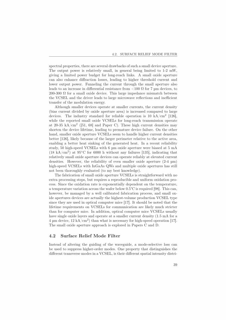
4.2. SURFACE RELIEF MODE FILTER
spectral properties, there are several drawbacks of such a small device aperture.The output power is relatively small, in general being limited to 1-2 mW,giving a limited power budget for long-reach links. A small oxide aperturecan also enhance diffraction losses, leading to higher threshold current andlower output power. Funneling the current through the small aperture alsoleads to an increase in differential resistance from <100 Ω for 7 μm devices, to200-300 Ω for a small oxide device. This large impedance mismatch betweenthe VCSEL and the driver leads to large microwave reflections and inefficienttransfer of the modulation energy.
Although smaller devices operate at smaller currents, the current density(bias current divided by oxide aperture area) is increased compared to largedevices. The industry standard for reliable operation is 10 kA/cm2 [126],while the reported small oxide VCSELs for long-reach transmission operateat 20-35 kA/cm2 ([51, 68] and Paper C). These high current densities mayshorten the device lifetime, leading to premature device failure. On the otherhand, smaller oxide aperture VCSELs seem to handle higher current densitiesbetter [126], likely because of the larger perimeter relative to the active area,enabling a better heat sinking of the generated heat. In a recent reliabilitystudy, 50 high-speed VCSELs with 6 μm oxide aperture were biased at 5 mA(18 kA/cm2) at 95◦C for 6000 h without any failures [135], indicating thatrelatively small oxide aperture devices can operate reliably at elevated currentdensities. However, the reliability of even smaller oxide aperture (2-4 μm)high-speed VCSELs with InGaAs QWs and multiple oxide apertures has stillnot been thoroughly evaluated (to my best knowledge).
The fabrication of small oxide aperture VCSELs is straightforward with noextra processing steps, but requires a reproducible and uniform oxidation pro-cess. Since the oxidation rate is exponentially dependent on the temperature,a temperature variation across the wafer below 0.5°C is required [98]. This can,however, be managed by a well calibrated fabrication process, and small ox-ide apertures devices are actually the highest-volume production VCSEL typesince they are used in optical computer mice [17]. It should be noted that thelifetime requirements on VCSELs for communication are likely much stricterthan for computer mice. In addition, optical computer mice VCSELs usuallyhave single oxide layers and operate at a smaller current density (1.5 mA for a4 μm device, 12 kA/cm2) than what is necessary for high-speed operation [17].The small oxide aperture approach is explored in Papers C and D.
4.2 Surface Relief Mode Filter
Instead of altering the guiding of the waveguide, a mode-selective loss canbe used to suppress higher-order modes. One property that distinguishes thedifferent transverse modes in a VCSEL, is their different spatial intensity distri-
39
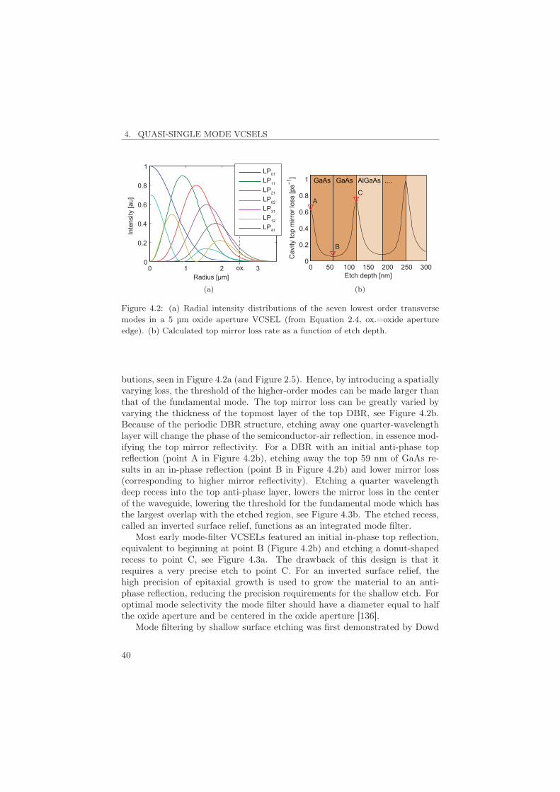
4. QUASI-SINGLE MODE VCSELS
0 1 2 30
0.2
0.4
0.6
0.8
1
Radius [μm]
Inte
nsity
[au]
ox.
LP01
LP11
LP21
LP02
LP31
LP12
LP41
(a)
0 50 100 150 200 250 3000
0.2
0.4
0.6
0.8
1
Etch depth [nm]
Cav
ity to
p m
irror
loss
[ps
]
B
AC
GaAs AlGaAs ....GaAs
(b)
Figure 4.2: (a) Radial intensity distributions of the seven lowest order transversemodes in a 5 μm oxide aperture VCSEL (from Equation 2.4, ox.=oxide apertureedge). (b) Calculated top mirror loss rate as a function of etch depth.
butions, seen in Figure 4.2a (and Figure 2.5). Hence, by introducing a spatiallyvarying loss, the threshold of the higher-order modes can be made larger thanthat of the fundamental mode. The top mirror loss can be greatly varied byvarying the thickness of the topmost layer of the top DBR, see Figure 4.2b.Because of the periodic DBR structure, etching away one quarter-wavelengthlayer will change the phase of the semiconductor-air reflection, in essence mod-ifying the top mirror reflectivity. For a DBR with an initial anti-phase topreflection (point A in Figure 4.2b), etching away the top 59 nm of GaAs re-sults in an in-phase reflection (point B in Figure 4.2b) and lower mirror loss(corresponding to higher mirror reflectivity). Etching a quarter wavelengthdeep recess into the top anti-phase layer, lowers the mirror loss in the centerof the waveguide, lowering the threshold for the fundamental mode which hasthe largest overlap with the etched region, see Figure 4.3b. The etched recess,called an inverted surface relief, functions as an integrated mode filter.
Most early mode-filter VCSELs featured an initial in-phase top reflection,equivalent to beginning at point B (Figure 4.2b) and etching a donut-shapedrecess to point C, see Figure 4.3a. The drawback of this design is that itrequires a very precise etch to point C. For an inverted surface relief, thehigh precision of epitaxial growth is used to grow the material to an anti-phase reflection, reducing the precision requirements for the shallow etch. Foroptimal mode selectivity the mode filter should have a diameter equal to halfthe oxide aperture and be centered in the oxide aperture [136].
Mode filtering by shallow surface etching was first demonstrated by Dowd
40
4.2. SURFACE RELIEF MODE FILTER
BC C
(a)
BA A
(b)
Figure 4.3: Schematic figure of surface-relief techniques illustrating the oxide aper-ture and the overlap of the three lowest-order modes (LP01, LP11 and LP21) for (a)donut-shaped surface relief etched from B to C, and (b) inverted surface relief etchedfrom A to B in 4.2b.
et al. in 1997, achieving single-mode emission for large aperture implantedVCSELs and a spectral narrowing for oxide-confined VCSELs [137]. Thetechnique was from the late 1990’s further developed mainly by ChalmersUniversity of Technology [128, 133, 136] and Ulm University [138–140]. Themode-filtering technique has successfully achieved single-mode VCSELs withoutput powers exceeding 6 mW [133, 140]. For applications such as gas sensing,where a single polarization is desired, a subwavelength grating surface reliefcan be used to achieve polarization-stable single-mode emission [128, 139]. Thesurface-relief method has also been applied to other material systems, for in-stance AlGaSb VCSELs emitting at 2.35 μm [141]. High-speed VCSELs withinverted surface reliefs are investigated in Papers E, F and G.
4.2.1 Effects on Static Characteristics
Since the shallow surface etching affects the top DBR reflectivity, the thresh-old current and slope efficiency are also affected. For an initial anti-phasetop DBR, the inverted surface-relief etching increases the overall top mirrorreflectivity, in effect lowering the threshold current and slope efficiency. Alarge reflectivity also leads to a longer photon lifetime, leading to an increasedinternal absorption rate, and stronger damping of the modulation response ac-companied by lower bandwidth [112] (as discussed in Section 3.4). A shorterphoton lifetime for lower damping requires a larger overall loss, while a suc-cessful mode discrimination still requires a large loss difference between pointsA and B in Figure 4.2b. This seems possible by for instance using fewer mirror
41

4. QUASI-SINGLE MODE VCSELS
pairs, as seen in Figure 4.2b. The top mirror loss is in general increased forfewer mirror pairs and the maximum loss difference between an anti-phase andin-phase reflection also increases.
42
Chapter 5
VCSEL Fabrication
The epitaxial VCSEL structures used in this work were grown by IQE EuropeLtd. using metal-organic chemical vapor deposition (MOCVD). Molecularbeam epitaxty (MBE) can also be used to grow the structure, but MOCVD isusually preferred for commercial production because of the higher throughput.In MOCVD gaseous organic compounds transport III-metals (Al, Ga, In) intothe reactor where they react with gaseous As (carried by the gas AsH3) andadsorb on the heated substrate. Doping is done by introducing Si or C into thereactor for n- and p-doping. After the growth of the epitaxial structure, thedevice processing starts. The different processing steps used in high-speed VC-SEL fabrication are briefly described in this chapter, followed by and overviewof the full VCSEL process.
5.1 Lithography
Most process steps in micro- and nanofabrication starts by patterning a pro-tective coating called a resist on the sample using lithography. The moststraightforward method is photolithography where a photoresist (a photosen-sitive polymer diluted with a solvent) is used. The viscous photoresist is dis-pensed onto the sample which is spun at a few thousand rounds per minute toform a thin film. The film thickness is on the order of one or a few micrometersdepending on the resist viscosity and spin speed. The resist is then baked ona hotplate to remove the solvent. To pattern the resist a glass plate with achromium pattern is manually aligned on top of the sample, shadowing certainareas as the sample is exposed with ultra-violet radiation at 400 nm. By usinga liquid developer, the exposed areas can be removed, leaving a pattern onthe sample. The manual alignment has an error margin of around 1 μm. If a
43
5. VCSEL FABRICATION
so-called negative resist is being used, the unexposed resist areas are insteadremoved. A third resist type is image reversal resist, commonly used for lift-offprocesses.
The wave nature of light prohibits definition of features smaller than λ/2by conventional photolithography. Standard contact photolithography with aresolution of approximately 1 μm, was used in this work [142]. More advancedphotolithography techniques such as phase shifted masks, enables the defini-tion of features smaller than 100 nm. However, such a process is not feasiblefor a flexible research environment, where electron-beam lithography is usedinstead. It works essentially the same way as photolithography, but insteadusing an electron-sensitive resist. The main difference is that instead of aUV lamp exposing the entire sample as once, an electron beam scans acrossthe sample, making this lithography technique a more time consuming serialprocess. Because of the very short electron wavelength, electron beam lithog-raphy can achieve a resolution down to 10 nm. The electron beam lithographysystem uses an automated alignment system that detects alignment marks onthe sample for near perfect alignment. Definition of small features in com-mercial production may also be done by nanoimprint lithography, where animprint resist is patterned with a stamp. Compared to the serial electronbeam lithography, nanoimprint is very fast, but manufacturing of the stampis expensive and it allows no process flexibility. Nanoimprint lithography hasfor instance been used to fabricate polarization-stable sub-wavelength gratingVCSELs [143].
5.2 Thin Film Deposition
Both dielectric and metal thin films are used in VCSEL processing. Dielectricmaterials such as SixNy (exact stoichiometry varies with deposition condi-tions), SiO2, amorphous Si and TiO2 are commonly used as electrical pas-sivation layers, hard masks for etching, and optical coatings, as well as toprotect surfaces during particular processing steps. Metal thin films are usedfor contacts on semiconductor material and bondpads. A lift-off process withan image-reversal photoresist is usually used for thin-film deposition. After de-position the image reversal resist is lifted off by immersion in heated solvents(usually acetone, methanol and isopropanol). For difficult lift-offs, acetonespray may be used, while ultrasonic bath should be avoided because of therisk of breaking the relatively brittle GaAs samples.
Dielectric materials are commonly deposited by plasma-enhanced chemicalvapor deposition (PECVD). Gases are injected into a vacuum chamber wherea plasma is generated by a plasma source as, for instance, an inductively-coupled plasma (ICP). Ions and reactive radicals from the plasma react onthe sample surface to form the thin film. The film thickness can be precisely
44
5.3. ETCHING
in-situ monitored by a laser interferometer. ICP-PECVD was used to depositSixNy to protect the top surface during oxidation and as a hardmask for mesaprocessing for mode filter VCSELs.
Metals thin films are conveniently deposited by electron-beam evaporation.An electron beam is used to heat the metal which evaporates and the metalvapor adsorbs on the sample. The deposition rate is accurately controlled bymonitoring the decrease in resonance frequency of a crystal as the depositedfilm thickness increases. This technique was used to deposit Ti/Pt/Au p-contacts and Ni/Ge/Au n-contacts.
Both dielectric and metal films can be deposited by sputtering. EnergeticAr ions generated in a plasma are accelerated towards a target and sputteraway atoms which are deposited on the sample. Sputtering has the advantageof a better step coverage than PECVD and electron beam evaporation, andwas therefore used to deposit Ti/Au bondpads in this work.
5.3 Etching
Removal of semiconductor material may be done by either dry or wet etching,depending on the requirements on etch rate, anisotropy and selectivity. Wetetching is inherently chemical where a reactive liquid dissolves the material.GaAs wet etchants usually contain one oxidizer that oxidizes the surface andone acid that then dissolves the oxide. Even though a high selectivity canbe achieved for certain material systems, the etched material usually etchesisotropically, meaning that for instance a VCSEL mesa etched by wet etchingwould have sloped sidewalls.
When vertical sidewalls are desired, dry-etching techniques are used. Ionsand radicals are created in a plasma and accelerated towards the sample byan electric field, where the ions sputter away material and the highly reac-tive radicals chemically etch the material. This gives the dry-etching processboth a physical and a chemical etch component. By changing the processparameters the plasma density and accelerating electric field may be varied,meaning that the chemical and physical process components may be individu-ally tuned in order to optimize the process. The etched material forms volatileproducts that leave the process chamber through the vacuum exhaust. In thiswork inductively coupled plasma reactive ion etching (ICP-RIE) was used toetch AlGaAs (using SiCl4/Ar and Cl2/Ar), SixNy (using NF3), and benzo-cyclobutene (BCB, using CF4/O2). The dry etching was done in the sametool as the PECVD and the etch depth can be in-situ monitored with a laserinterferometer.
To achieve a very precise etch depth for the surface-relief mode filters,Ar ion-beam milling was first used. Ar ions are generated in a plasma andaccelerated towards the surface, sputtering away material. While the etch
45
5. VCSEL FABRICATION
rate for ICP-RIE may vary due to different conditions that affect the sensitivechemical component of the etch, the ion beam milling is purely physical. Thisenables a very stable and reproducible etch rate, allowing precise etch depthsby timed etching. One drawback is that the etched material does not formvolatile products, and may redeposit somewhere else on the sample. Papers Eand F used Ar ion beam milling to etch the mode filters, while Paper G usedICP-RIE using the laser interferometer for in-situ monitoring.
5.4 Wet Oxidation
In order to form the oxide aperture, the etched mesa sidewalls are exposed tohot water vapor at 420°C. Nitrogen gas is fed through a bubbler and carries thewater vapor into a furnace. Through a glass window in the top of the furnacechamber, the oxidation can be in-situ observed by imaging the sample with aninfrared LED through a microscope onto a CCD camera. The oxide aperturescan be discerned by the difference in reflectivity between the oxidized and non-oxidized areas. The oxidation process is highly sensitive to the temperatureand even a small temperature gradient across the sample will lead to a varyingoxidation rate and an undesired spread in oxide apertures across the chip [98].To avoid this, the chip can be turned 180°after half the process time. The ox-idation rate for Al0.98Ga0.02As is approximately 0.25 μm/min in our standardoxidation process. Layers with a lower Al content will oxidize much slower,but neighboring layers such as Al0.90Ga0.10As may oxidize vertically from the98% layer, making the oxide layer thicker, see Figure 3.3.
5.5 High-Speed VCSEL Process
Before processing started, the large 3" wafer was cleaved into 8 x 10 mm chipsand cleaned. As a first step Ti/Pt/Au alignment marks and top p-contact ringswere deposited by electron-beam evaporation (Figure 5.1a). Then a SixNy filmwas blanket deposited to protect the top surface during the later wet oxida-tion step. The mesas were defined by electron-beam or photolithography. Themesa etching was done with ICP-RIE to first remove the protective SixNy (us-ing NF3), and then etch the AlGaAs with Ar/SiCl4 and Ar/Cl2. A precise etchdepth of 3.3-3.5 μm was obtained by using the in-situ laser interferometer inorder to expose the oxide layers, but not the AlAs layers of the bottom DBR.Without breaking vacuum, the sample was moved to another chamber, whereICP-PECVD was used to deposit another layer of SixNy. After lifting off thephotoresist, the chip was thereby covered in SixNy without any AlGaAs beingexposed to air (Figure 5.1b). The SixNy on the sidewalls was then removed byphotolithography and ICP-RIE etching with NF3, which has a high selectivity
46
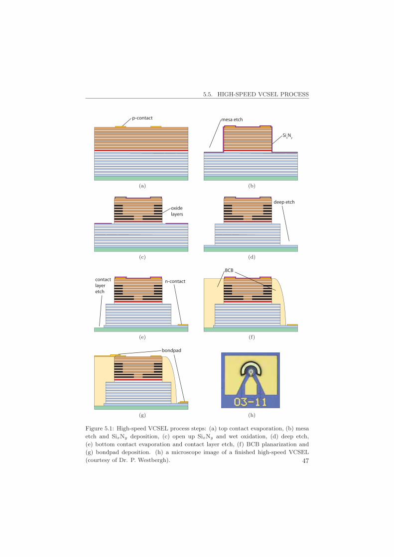
5.5. HIGH-SPEED VCSEL PROCESS
p-contact
(a)
SixNy
mesa etch
(b)
oxidelayers
(c)
deep etch
(d)
n-contactcontactlayeretch
(e)
BCB
(f)
bondpad
(g) (h)
Figure 5.1: High-speed VCSEL process steps: (a) top contact evaporation, (b) mesaetch and SixNy deposition, (c) open up SixNy and wet oxidation, (d) deep etch,(e) bottom contact evaporation and contact layer etch, (f) BCB planarization and(g) bondpad deposition. (h) a microscope image of a finished high-speed VCSEL(courtesy of Dr. P. Westbergh). 47
5. VCSEL FABRICATION
(∼100) to AlGaAs. The oxidation at 420°C takes around 40 min, dependingon the exact Al-content, and was monitored using the in-situ microscope (Fig-ure 5.1c). By using different mesa sizes, oxide aperture diameters from 3 to9 μm were obtained. After photolithography, the bottom mesa was etched toreach the n-contact layer, using again NF3 to remove the SixNy, and Ar/SiCl4and Ar/Cl2 to etch the AlGaAs (Figure 5.1d). The bottom Ni/Ge/Au n-contacts were deposited by electron-beam evaporation and annealed for 30 sat 430°C in an N2 atmosphere. Following this step the n-doped GaAs con-tact layer was removed under the future p-bondpad by photolithography andICP-RIE etching (Figure 5.1e). A thick layer of BCB was spun over the mesato planarize the structure (Figure 5.1f). The BCB is photosensitive, enablingopening up of the BCB covering the n-contact and mesa by photolithography.However, spreading of the UV-light in the thick BCB gives poor contrast,and prevents complete opening up by photolithography only. The last BCBmust therefore be etched away using ICP-RIE etching with CF4/O2. It isvery important to remove all BCB, and at the same time not etch throughthe protective SixNy. As final steps, the protective SixNy was removed withICP-RIE and Ti/Au bondpads were deposited by sputtering to achieve a goodstep-coverage into the n-contact trench in the BCB (Figure 5.1g).
5.5.1 Surface-Relief Processing
There are a few special requirements on the processing of mode-filter VC-SELs. Firstly, the epitaxial growth must have nm-precision in order to havean anti-phase top DBR reflection with a high mirror loss (see Section 4.2).For the processing of the mode filter it is necessary to achieve a good align-ment between the oxide aperture and the surface relief, as well as a preciseetch depth (Figure 4.2b). Near perfect alignment is obtained by using electron-beam lithography to define the mode filters, aligned to etched alignment marksdefined simultaneously with the mesas. Another option would be to use a self-aligned process, where the mesa edge, which will define the oxide aperture,and the mode filter is defined by a donut-shaped hard mask [138]. However,because of variations in oxide aperture due to a varying oxidation rate, themode filters were defined and etched as the very last process step. This al-lowed matching of every oxide aperture with an appropriate mode filter. It iscritical that the VCSEL top surface, with its anti-phase reflection, is carefullyprotected during the processing since accidental oxidation or etching of just afew nanometers will impact the mode filter performance.
48
Chapter 6
Monolithic Multi-Wavelength VCSEL Arraysusing High-Contrast Gratings
By proper design of the HCG-VCSEL cavity, the resonance wavelength canbe set in a single lithography step by defining HCGs with different period andduty cycle. Using this effect to design multi-wavelength arrays with HCG-VCSELs was first proposed by Kim et al. in 2007 [144]. Such devices havesince then been designed and experimentally demonstrated by optical pumpingexperiments [145]. This thesis presents the first demonstration of wavelength-setting of electrically-injected HCG-VCSELs using the grating parameters (Pa-per H). This chapter starts with a review of different techniques to realizemonolithic multi-wavelength VCSEL arrays, followed by a presentation of theimportant properties of HCGs and details on the design of multi-wavelengthHCG-VCSELs.
6.1 Monolithic Multi-Wavelength VCSEL Arrays
A low-cost monolithically integrated multi-wavelength light source is highlydesired for WDM in optical interconnects. Small variations in VCSEL wave-lengths, on the order of a couple of nm, can be realized by using VCSELswith different oxide aperture [146], or biasing the VCSELs at different cur-rents [147]. But for uncooled operation a wider channel spacing is needed.Different designs and technologies for fabricating multi-wavelength VCSELarrays have been explored since the early 1990’s. In general all techniqueswork by modifying the effective cavity length and thereby the resonance wave-length. Early attempts utilized nonuniform epitaxial growth by MBE [148],and MOCVD growth on patterned substrates using non-uniform gas flow in
49
6. MONOLITHIC MULTI-WAVELENGTH HCG-VCSEL ARRAYS
etched grooves [149]. The latter technique was used to demonstrate VCSELarrays with an impressive wavelength span of 192 nm from 960-1160 nm, butrequires complicated epitaxial growth techniques [150]. Strained suspendedcantilevers with top DBRs where the cavity length depends on the cantileverlength have also been explored [151]. These techniques successfully demon-strated multi-wavelength VCSEL arrays across the wafer, but are not suitablefor small-footprint dense VCSEL arrays with arbitrary layout. Better wave-length control and layout flexibility can be achieved by post-growth intra-cavity modifications using micro- and nanofabrication techniques. By verti-cally oxidizing a thick AlGaAs layer, devices with different cavity length canbe lithographically defined [152]. However, introducing thick oxide layers maylead to issues with thermal conductivity. Another technique is adjusting thethickness of a phase-tuning layer inside the VCSEL cavity. By using a di-electric top DBR, the VCSEL cavity can be accessed during fabrication. Theresonance wavelength can be easily modified by varying the thickness of thecavity or the first DBR layer by either deposition or etching [153–156]. How-ever, these intra-cavity techniques require at least log2(N) highly accurateetching or deposition steps, where N is the number of channels desired. Pre-cise thickness control is necessary for accurate wavelength control to fabricateVCSEL arrays with wavelengths falling within the desired wavelength slots ofthe WDM channels [157].
A design utilizing high-contrast gratings (HCGs) for lithographically de-fined post-growth wavelength setting was proposed in 2007 by Kim et al. [144],and further described in 2010 by Karagodsky et al. [158]. By fabricatingHCGs with different parameters (period, duty cycle), the grating reflectionphase may be tailored, introducing a certain phase shift in the cavity thatdetermines the resonance wavelength. Such devices have previously been de-signed and proven by optical pumping experiments [145], using VCSELs withan InP active region and wafer bonded mirrors of Si HCGs buried in SiO2.The optical pumping realized a wavelength span of 12 nm around 1.55μm.Electrically-injected wavelength-setting of HCG-VCSELs using the grating pa-rameters have so far not been published. The main challenge is that HCGswith exceptionally high reflectivities are needed as further described in thischapter. A monolithic multi-wavelength HCG-VCSEL array was presented byRao et al. in 2010 [159]. However, the wavelength was set by varying the airgap thickness below a suspended HCG using time-controlled wet etching, andnot by changing the grating parameters.
In addition to controlling the cavity length, an active region with a broadoptical gain is desired to design VCSEL arrays with a wide wavelength spanand uniform device performance. By using QWs with different widths, thesame active region could support lasing over a 90 nm span from 766 nm in atunable grating-coupled ring laser [160]. MOVCD growth on patterned sub-
50
6.2. HIGH-CONTRAST GRATINGS
strates, mentioned earlier, realized QWs with different widths, enabling theimpressive wavelength span of 192 nm from 960-1160 nm [150]. Hence, eventhough they were grown simultaneously, the different VCSELs in the arrayhave different active regions. Using identical-quantum-well active regions, las-ing over a span of ∼20-30 nm is commonly obtained in monolithic short-wavelength multi-wavelength VCSEL arrays [148, 152–154]. This wavelengthspan could enable 3-4 WDM channels with 10 nm channel spacing. However,nonuniform device performance would likely be a significant issue, and maywell prevent high-speed (>25 Gbit/s) operation.
6.2 High-Contrast Gratings
High-contrast gratings (HCGs) are gratings of a high-refractive index materialsurrounded by low-index material, see Figure 6.1. For sub-wavelength HCGperiods, remarkable properties such as close to 100% reflectivity with a widestop-band can be obtained for certain HCG parameters [161]. Highly reflectiveHCGs were first proposed and demonstrated by the group of Prof. ConnieJ. Chang-Hasnain at the University of California, Berkeley in 2004 [162, 163].The first VCSEL with an HCG-based top mirror was demonstrated by the samegroup in 2007 [164]. Since then HCGs have been proposed and fabricated in awide range of materials for different wavelengths ranging from 450 to 2300 nm[163, 165–167]. Already from the start, HCGs attracted a large interest asmirrors for InP-based VCSELs emitting at 1310 or 1550 nm [166, 168], sinceepitaxial DBRs in this material system have a small index difference betweenthe high and low-refractive index material, resulting in long growth times forthe thick DBRs and a narrow reflection stopband. The small mass of the thinHCG compared to a ∼30-pair DBR has also enabled micro-electro-mechanicalsystems (MEMS)-VCSELs with ultra-fast electrostatic tuning [169].
The phase of the HCG reflection and transmission is highly dependenton the HCG parameters, for instance grating period and duty cycle. Thiseffect is used in this work to design and demonstrate monolithically integratedmulti-wavelength VCSEL arrays. The same phenomena can also be used todesign and fabricate chirped-period HCGs with arbitrary spatially varyingphase, enabling the design of flat lenses with high numerical aperture [170].Furthermore, HCGs have several additional interesting properties. They maybe used both as reflectors, vertical to in-plane couplers, or a combinationthereof [171], making them highly interesting for applications in small-footprintintegrated optics in both silicon photonics and heterogeneously integrated III-V on silicon [171–173].
51
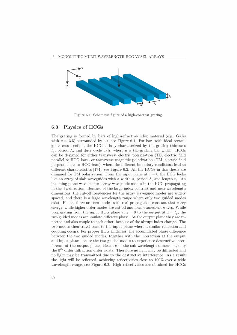
6. MONOLITHIC MULTI-WAVELENGTH HCG-VCSEL ARRAYS
x
y
z
a
tg
Figure 6.1: Schematic figure of a high-contrast grating.
6.3 Physics of HCGs
The grating is formed by bars of high-refractive-index material (e.g. GaAswith n ≈ 3.5) surrounded by air, see Figure 6.1. For bars with ideal rectan-gular cross-section, the HCG is fully characterized by the grating thicknesstg, period Λ, and duty cycle a/Λ, where a is the grating bar width. HCGscan be designed for either transverse electric polarization (TE, electric fieldparallel to HCG bars) or transverse magnetic polarization (TM, electric fieldperpendicular to HCG bars), where the different boundary conditions lead todifferent characteristics [174], see Figure 6.2. All the HCGs in this thesis aredesigned for TM polarization. From the input plane at z = 0 the HCG lookslike an array of slab waveguides with a width a, period Λ, and length tg. Anincoming plane wave excites array waveguide modes in the HCG propagatingin the +z-direction. Because of the large index contrast and near-wavelengthdimensions, the cut-off frequencies for the array waveguide modes are widelyspaced, and there is a large wavelength range where only two guided modesexist. Hence, there are two modes with real propagation constant that carryenergy, while higher order modes are cut-off and form evanescent waves. Whilepropagating from the input HCG plane at z = 0 to the output at z = tg, thetwo guided modes accumulate different phase. At the output plane they are re-flected and also couple to each other, because of the abrupt index change. Thetwo modes then travel back to the input plane where a similar reflection andcoupling occurs. For proper HCG thickness, the accumulated phase differencebetween the two guided modes, together with the interaction at the outputand input planes, cause the two guided modes to experience destructive inter-ference at the output plane. Because of the sub-wavelength dimension, onlythe 0th order diffraction order exists. Therefore no light may be diffracted andno light may be transmitted due to the destructive interference. As a resultthe light will be reflected, achieving reflectivities close to 100% over a widewavelength range, see Figure 6.2. High reflectivities are obtained for HCGs
52
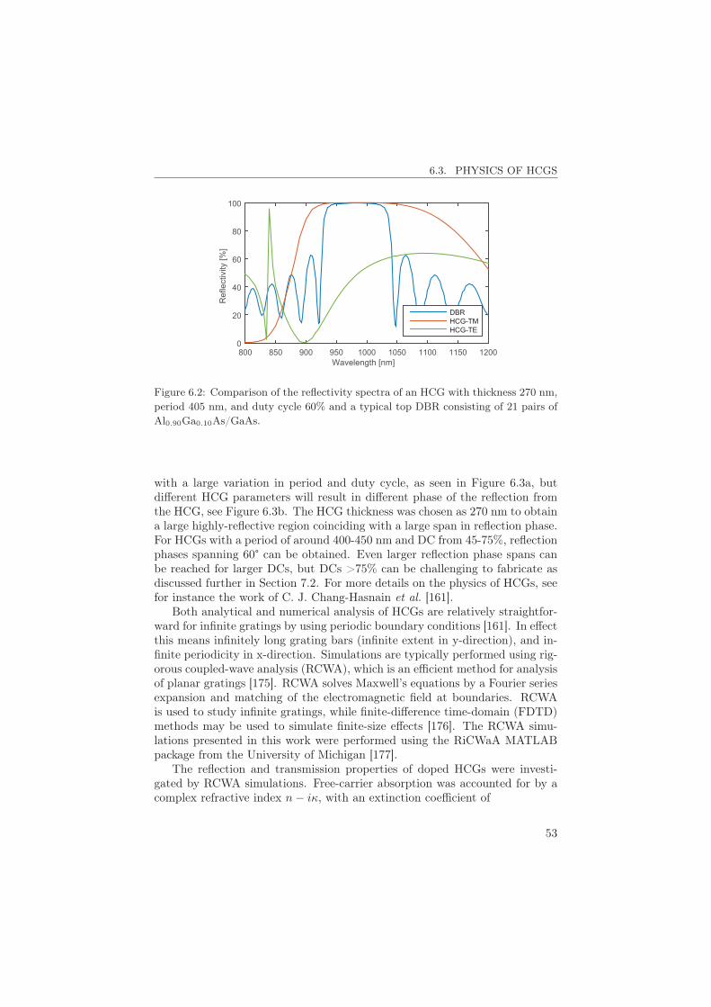
6.3. PHYSICS OF HCGS
Wavelength [nm]800 850 900 950 1000 1050 1100 1150 1200
Ref
lect
ivity
[%]
0
20
40
60
80
100
DBRHCG-TMHCG-TE
Figure 6.2: Comparison of the reflectivity spectra of an HCG with thickness 270 nm,period 405 nm, and duty cycle 60% and a typical top DBR consisting of 21 pairs ofAl0.90Ga0.10As/GaAs.
with a large variation in period and duty cycle, as seen in Figure 6.3a, butdifferent HCG parameters will result in different phase of the reflection fromthe HCG, see Figure 6.3b. The HCG thickness was chosen as 270 nm to obtaina large highly-reflective region coinciding with a large span in reflection phase.For HCGs with a period of around 400-450 nm and DC from 45-75%, reflectionphases spanning 60° can be obtained. Even larger reflection phase spans canbe reached for larger DCs, but DCs >75% can be challenging to fabricate asdiscussed further in Section 7.2. For more details on the physics of HCGs, seefor instance the work of C. J. Chang-Hasnain et al. [161].
Both analytical and numerical analysis of HCGs are relatively straightfor-ward for infinite gratings by using periodic boundary conditions [161]. In effectthis means infinitely long grating bars (infinite extent in y-direction), and in-finite periodicity in x-direction. Simulations are typically performed using rig-orous coupled-wave analysis (RCWA), which is an efficient method for analysisof planar gratings [175]. RCWA solves Maxwell’s equations by a Fourier seriesexpansion and matching of the electromagnetic field at boundaries. RCWAis used to study infinite gratings, while finite-difference time-domain (FDTD)methods may be used to simulate finite-size effects [176]. The RCWA simu-lations presented in this work were performed using the RiCWaA MATLABpackage from the University of Michigan [177].
The reflection and transmission properties of doped HCGs were investi-gated by RCWA simulations. Free-carrier absorption was accounted for by acomplex refractive index n− iκ, with an extinction coefficient of
53
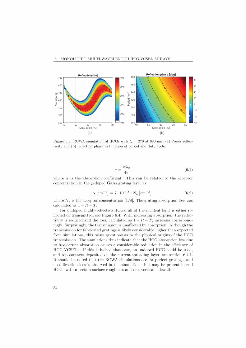
6. MONOLITHIC MULTI-WAVELENGTH HCG-VCSEL ARRAYS
Duty cycle [%]40 50 60 70 80
Per
iod
[nm
]
360
380
400
420
440
460
480
99.8
99.8
99.8
99.8
Reflectivity [%]
<99
99.2
99.4
99.6
99.8
100
(a)P
erio
d [n
m]
Duty cycle [%]40 50 60 70 80
360
380
400
420
440
460
480
-60-40
-20
-20
0 20
20
40
4060
80
Reflection phase [deg]
-60
-40
-20
0
20
40
60
80
(b)
Figure 6.3: RCWA simulation of HCGs with tg = 270 at 980 nm. (a) Power reflec-tivity and (b) reflection phase as function of period and duty cycle.
κ =αλ0
4π, (6.1)
where α is the absorption coefficient. This can be related to the acceptorconcentration in the p-doped GaAs grating layer as
α[cm−1
]= 7 · 10−18 ·Na
[cm−3
], (6.2)
where Na is the acceptor concentration [178]. The grating absorption loss wascalculated as 1−R− T .
For undoped highly-reflective HCGs, all of the incident light is either re-flected or transmitted, see Figure 6.4. With increasing absorption, the reflec-tivity is reduced and the loss, calculated as 1 − R − T , increases correspond-ingly. Surprisingly, the transmission is unaffected by absorption. Although thetransmission for fabricated gratings is likely considerable higher than expectedfrom simulations, this raises questions as to the physical origins of the HCGtransmission. The simulations thus indicate that the HCG absorption loss dueto free-carrier absorption causes a considerable reduction in the efficiency ofHCG-VCSELs. If this is indeed that case, an undoped HCG could be used,and top contacts deposited on the current-spreading layer, see section 6.4.1.It should be noted that the RCWA simulations are for perfect gratings, andno diffraction loss is observed in the simulations, but may be present in realHCGs with a certain surface roughness and non-vertical sidewalls.
54
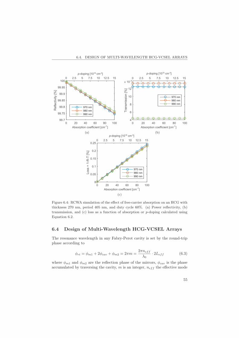
6.4. DESIGN OF MULTI-WAVELENGTH HCG-VCSEL ARRAYS
Absorption coefficient [cm-1]0 20 40 60 80 100
Ref
lect
ivity
[%]
99.7
99.75
99.8
99.85
99.9
99.95
100
970 nm980 nm990 nm
0 2.5 5 7.5 10 12.5 15p-doping [1018 cm-3]
(a)
Absorption coefficient [cm-1]0 20 40 60 80 100
Tran
smis
sion
[%]
x 10-3
4
6
8
10
12
970 nm980 nm990 nm
0 2.5 5 7.5 10 12.5 15p-doping [1018 cm-3]
(b)
Absorption coefficient [cm-1]0 20 40 60 80 100
Loss
= 1
-R-T
[%]
0
0.05
0.1
0.15
0.2
0.25
970 nm980 nm990 nm
0 2.5 5 7.5 10 12.5 15p-doping [1018 cm-3]
(c)
Figure 6.4: RCWA simulation of the effect of free-carrier absorption on an HCG withthickness 270 nm, period 405 nm, and duty cycle 60%. (a) Power reflectivity, (b)transmission, and (c) loss as a function of absorption or p-doping calculated usingEquation 6.2.
6.4 Design of Multi-Wavelength HCG-VCSEL Arrays
The resonance wavelength in any Fabry-Perot cavity is set by the round-tripphase according to
φrt = φm1 + 2φcav + φm2 = 2πm =2πneff
λ0· 2Leff (6.3)
where φm1 and φm2 are the reflection phase of the mirrors, φcav is the phaseaccumulated by traversing the cavity, m is an integer, neff the effective mode
55
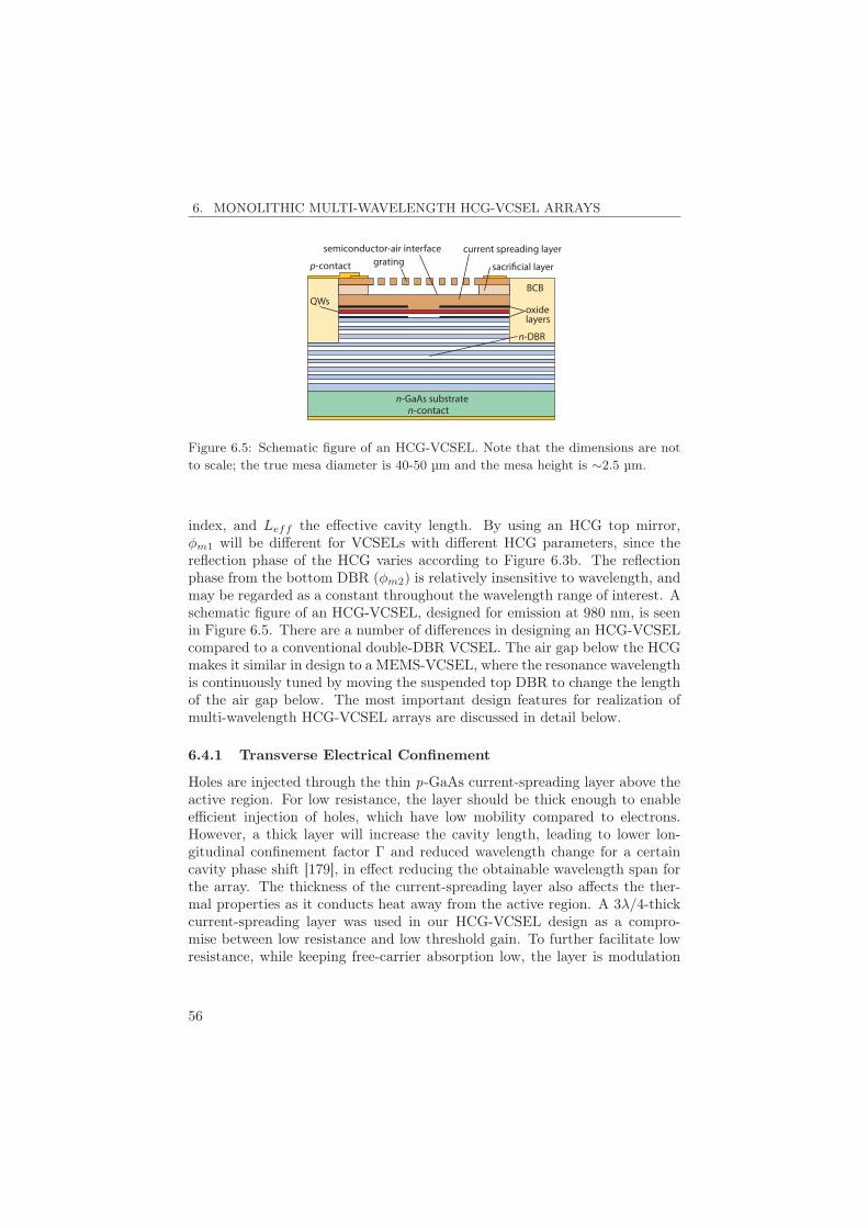
6. MONOLITHIC MULTI-WAVELENGTH HCG-VCSEL ARRAYS
n-GaAs substrate
gratingp-contact
current spreading layer
BCBQWs
oxide layers
n-DBR
n-contact
sacrificial layer
semiconductor-air interface
Figure 6.5: Schematic figure of an HCG-VCSEL. Note that the dimensions are notto scale; the true mesa diameter is 40-50 μm and the mesa height is ∼2.5 μm.
index, and Leff the effective cavity length. By using an HCG top mirror,φm1 will be different for VCSELs with different HCG parameters, since thereflection phase of the HCG varies according to Figure 6.3b. The reflectionphase from the bottom DBR (φm2) is relatively insensitive to wavelength, andmay be regarded as a constant throughout the wavelength range of interest. Aschematic figure of an HCG-VCSEL, designed for emission at 980 nm, is seenin Figure 6.5. There are a number of differences in designing an HCG-VCSELcompared to a conventional double-DBR VCSEL. The air gap below the HCGmakes it similar in design to a MEMS-VCSEL, where the resonance wavelengthis continuously tuned by moving the suspended top DBR to change the lengthof the air gap below. The most important design features for realization ofmulti-wavelength HCG-VCSEL arrays are discussed in detail below.
6.4.1 Transverse Electrical Confinement
Holes are injected through the thin p-GaAs current-spreading layer above theactive region. For low resistance, the layer should be thick enough to enableefficient injection of holes, which have low mobility compared to electrons.However, a thick layer will increase the cavity length, leading to lower lon-gitudinal confinement factor Γ and reduced wavelength change for a certaincavity phase shift [179], in effect reducing the obtainable wavelength span forthe array. The thickness of the current-spreading layer also affects the ther-mal properties as it conducts heat away from the active region. A 3λ/4-thickcurrent-spreading layer was used in our HCG-VCSEL design as a compro-mise between low resistance and low threshold gain. To further facilitate lowresistance, while keeping free-carrier absorption low, the layer is modulation
56
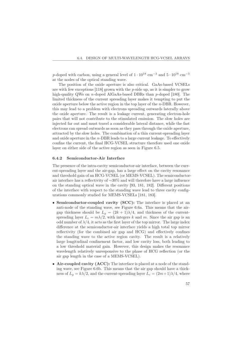
6.4. DESIGN OF MULTI-WAVELENGTH HCG-VCSEL ARRAYS
p-doped with carbon, using a general level of 1 · 1018 cm−3 and 5 · 1018 cm−3
at the nodes of the optical standing wave.The position of the oxide aperture is also critical. GaAs-based VCSELs
are with few exceptions [118] grown with the p-side up, as it is simpler to growhigh-quality QWs on n-doped AlGaAs-based DBRs than p-doped [180]. Thelimited thickness of the current spreading layer makes it tempting to put theoxide aperture below the active region in the top layer of the n-DBR. However,this may lead to a problem with electrons spreading outwards laterally abovethe oxide aperture. The result is a leakage current, generating electron-holepairs that will not contribute to the stimulated emission. The slow holes areinjected far out and must travel a considerable lateral distance, while the fastelectrons can spread outwards as soon as they pass through the oxide aperture,attracted by the slow holes. The combination of a thin current-spreading layerand oxide aperture in the n-DBR leads to a large current leakage. To effectivelyconfine the current, the final HCG-VCSEL structure therefore used one oxidelayer on either side of the active region as seen in Figure 6.5.
6.4.2 Semiconductor-Air Interface
The presence of the intra-cavity semiconductor-air interface, between the curr-ent-spreading layer and the air-gap, has a large effect on the cavity resonanceand threshold gain of an HCG-VCSEL (or MEMS-VCSEL). The semiconductor-air interface has a reflectivity of ∼30% and will therefore have a large influenceon the standing optical wave in the cavity [93, 181, 182]. Different positionsof the interface with respect to the standing wave lead to three cavity config-urations commonly studied for MEMS-VCSELs [181, 183].
• Semiconductor-coupled cavity (SCC): The interface is placed at ananti-node of the standing wave, see Figure 6.6a. This means that the air-gap thickness should be Lg = (2k + 1)λ/4, and thickness of the current-spreading layer Lc = mλ/2, with integers k and m. Since the air gap is anodd number of λ/4, it acts as the first layer of the top mirror. The large indexdifference at the semiconductor-air interface yields a high total top mirrorreflectivity (for the combined air gap and HCG) and effectively confinesthe standing wave to the active region cavity. The result is a relativelylarge longitudinal confinement factor, and low cavity loss, both leading toa low threshold material gain. However, this design makes the resonancewavelength relatively unresponsive to the phase of HCG reflection (or theair gap length in the case of a MEMS-VCSEL).
• Air-coupled cavity (ACC): The interface is placed at a node of the stand-ing wave, see Figure 6.6b. This means that the air gap should have a thick-ness of Lg = kλ/2, and the current-spreading layer Lc = (2m+1)λ/4, where
57
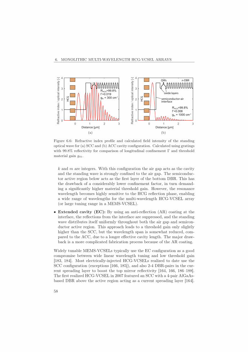
6. MONOLITHIC MULTI-WAVELENGTH HCG-VCSEL ARRAYS
Distance [μm]0 1 2 3R
efra
ctiv
e in
dex
/ opt
ical
inte
nsity
[-]
0
1
2
3
4
HCG
RHCG=99.8%=0.019
gth = 300 cm-1
(a)
Distance [μm]0 1 2 3R
efra
ctiv
e in
dex
/ opt
ical
inte
nsity
[-]
0
1
2
3
4
HCG
RHCG=99.8%=0.006
gth = 1000 cm-1
QWs
oxide layers
semiconductor-airinterface
n-DBR
(b)
Figure 6.6: Refractive index profile and calculated field intensity of the standingoptical wave for (a) SCC and (b) ACC cavity configuration. Calculated using gratingswith 99.8% reflectivity for comparison of longitudinal confinement Γ and thresholdmaterial gain gth.
k and m are integers. With this configuration the air gap acts as the cavityand the standing wave is strongly confined to the air gap. The semiconduc-tor active region below acts as the first layer of the bottom DBR. This hasthe drawback of a considerably lower confinement factor, in turn demand-ing a significantly higher material threshold gain. However, the resonancewavelength becomes highly sensitive to the HCG reflection phase, enablinga wide range of wavelengths for the multi-wavelength HCG-VCSEL array(or large tuning range in a MEMS-VCSEL).
• Extended cavity (EC): By using an anti-reflection (AR) coating at theinterface, the reflections from the interface are suppressed, and the standingwave distributes itself uniformly throughout both the air gap and semicon-ductor active region. This approach leads to a threshold gain only slightlyhigher than the SCC, but the wavelength span is somewhat reduced, com-pared to the ACC, due to a longer effective cavity length. The major draw-back is a more complicated fabrication process because of the AR coating.
Widely tunable MEMS-VCSELs typically use the EC configuration as a goodcompromise between wide linear wavelength tuning and low threshold gain[183, 184]. Most electrically-injected HCG-VCSELs realized to date use theSCC configuration (exceptions [166, 185]), and also 2-4 DBR-pairs in the cur-rent spreading layer to boost the top mirror reflectivity [164, 166, 186–188].The first realized HCG-VCSEL in 2007 featured an SCC with a 4-pair AlGaAs-based DBR above the active region acting as a current spreading layer [164].
58
6.4. DESIGN OF MULTI-WAVELENGTH HCG-VCSEL ARRAYS
Even though the authors claim that enough reflectivity could be provided bythe HCG itself, a 4-pair DBR with Al0.90Ga0.10As/Al0.12Ga0.88As has a re-flectivity of about 70% (from transfer matrix calculations [92]), and thereforesignificantly increases the top mirror reflectivity. The combination of a SCCand a 4-pair DBR makes the VCSEL rather insensitive to the HCG phase,with a wavelength change of about 2 nm for changes in period and duty cycle[187, 189].
HCGs have also been used as the top mirror for tunable MEMS-VCSELs.Also here most designs feature an SCC, and a few DBR-pairs in the current-spreading layer, in order to get low enough threshold gain to reach lasing[169, 188]. The only exception is [185], which demonstrated a MEMS HCG-VCSEL with an EC configuration with an oxidized Al0.98Ga0.02As layer as anAR coating, and no DBR-pairs in the current-spreading layer.
The HCG-VCSELs in this work use the ACC configuration in order toobtain a large wavelength span from the different HCG reflection phases (Fig-ure 6.3b). Owing to the high threshold gain, this configuration has in the pastoften been considered impractical for MEMS-VCSELs [183]. In order to reachlasing in our HCG-VCSELs, we must achieve the needed top mirror reflectivitywith only the HCG, without any assistance from the semiconductor-air inter-face or extra DBR-pairs. For comparison, for HCG-VCSELs with 99.8% HCGreflectivity, the threshold material gain is rather low at 300 cm−1 for the SCC,while the ACC requires 1000 cm−1 to reach threshold, see Figure 6.6. In or-der to reach threshold, HCGs with exceptionally high reflectivity are thereforerequired.
6.4.3 Wavelength-Setting and Threshold Material Gain
The wavelength setting and threshold characteristics of HCG-VCSELs usingHCGs with different period/duty cycle combinations were investigated by a1-D transfer-matrix method [92], where the HCG is replaced by an interfacehaving the properties obtained from RCWA grating simulations. One suchcalculation can be seen in Figure 6.6b, and results for HCG-VCSELs withdifferent HCGs can be seen in Figure 6.7. Each different HCG sets the res-onance frequency and threshold gain depending on its parameters, so eachpoint in Figure 6.7 represents a certain HCG-VCSEL design, with its corre-sponding threshold gain and resonance wavelength. A free-carrier absorptionof 35 cm−1, equivalent to a p-doping at 5 · 1018 cm−3, was included in thegrating for the RCWA simulations. The HCG thickness of tg = 270 nm waschosen for the TM-HCGs since it results in a wide low-threshold-gain region,see Figure 6.7a. By varying both grating period and duty cycle, resonancewavelengths from 960-1000 nm are possible, while keeping the threshold mate-rial gain <1000 cm−1. It should be noted that the material gain discussed in
59
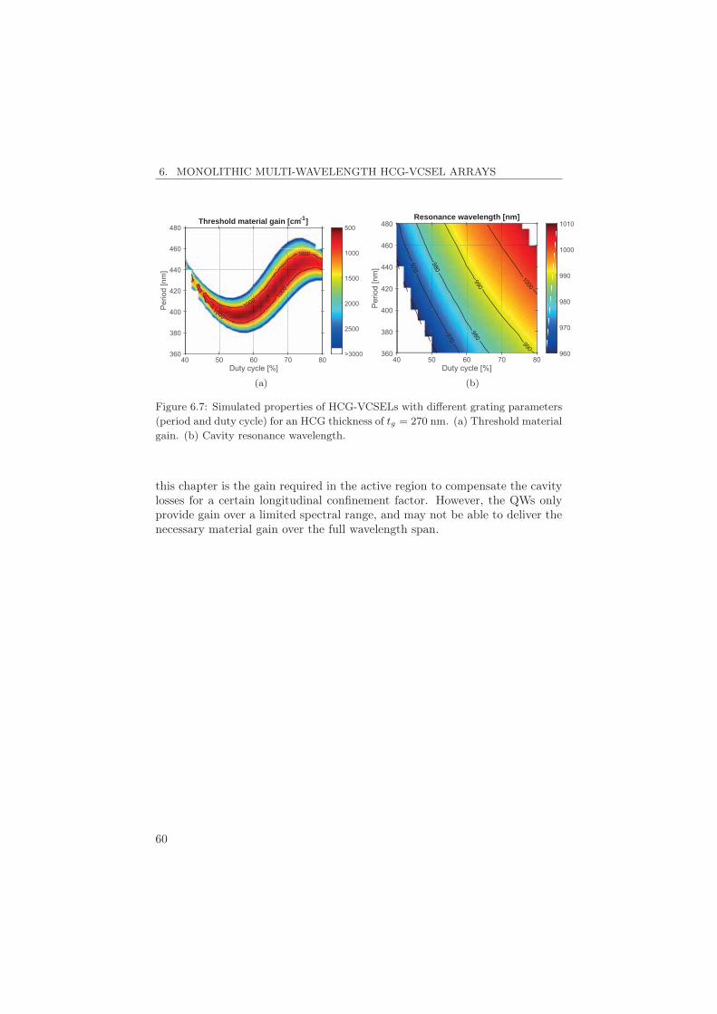
6. MONOLITHIC MULTI-WAVELENGTH HCG-VCSEL ARRAYS
Duty cycle [%]40 50 60 70 80
Per
iod
[nm
]
360
380
400
420
440
460
480
1000
10001000
1000
Threshold material gain [cm-1]500
1000
1500
2000
2500
>3000
(a)
Duty cycle [%]40 50 60 70 80
Per
iod
[nm
]
360
380
400
420
440
460
480
970
970
980
980990
9901000
Resonance wavelength [nm]
960
970
980
990
1000
1010
(b)
Figure 6.7: Simulated properties of HCG-VCSELs with different grating parameters(period and duty cycle) for an HCG thickness of tg = 270 nm. (a) Threshold materialgain. (b) Cavity resonance wavelength.
this chapter is the gain required in the active region to compensate the cavitylosses for a certain longitudinal confinement factor. However, the QWs onlyprovide gain over a limited spectral range, and may not be able to deliver thenecessary material gain over the full wavelength span.
60
Chapter 7
HCG Fabrication
High-contrast gratings have sometimes been described and demonstrated astolerant to processing imperfections [187]. While this has irrefutably beenproven for HCG-VCSELs with a hybrid DBR-HCG top mirror and SCC con-figuration, the highly reflective gratings needed for multi-wavelength HCG-VCSEL arrays must be clean with little residue, close to rectangular cross-section, and low grating edge roughness. These demands make the HCG fab-rication a challenging and delicate process. A schematic process flow for HCGfabrication is shown in Figure 7.1. First, the gratings are defined by electron-beam lithography. If a SixNy hard mask is used, the HCG pattern is trans-ferred into the SixNy by dry etching. The gratings are then dry etched throughthe grating layer down to the sacrificial layer using either the hard mask oronly the resist mask. The remaining mask is removed, and the sacrificial layeris etched away by a selective wet etch. After the etch, the gratings are notdried in air, as the grating bars would bend and stick to each other by surfacetension. Instead critical point drying must be used, where the rinsing liquidis replaced by liquid CO2 at high pressure, which is then removed without aliquid-gas phase transition.
A highly selective wet etch is needed to remove the sacrificial layer andunderetch the grating. This makes the choice of material combination forthe grating and sacrificial layers important. In addition to enable highly-selective wet etching, the materials must also be lattice matched to avoid strainwhich may lead to buckling of the suspended HCG bars. Two different grat-ing/sacrificial layer material combinations were evaluated; GaAs/In0.49Ga0.51Pfor 980 nm HCGs, and Al0.45Ga0.55As/GaAs for 850 nm HCGs. All scanning-electron microscope (SEM) images in this chapter are images of 980 nm GaAs
61
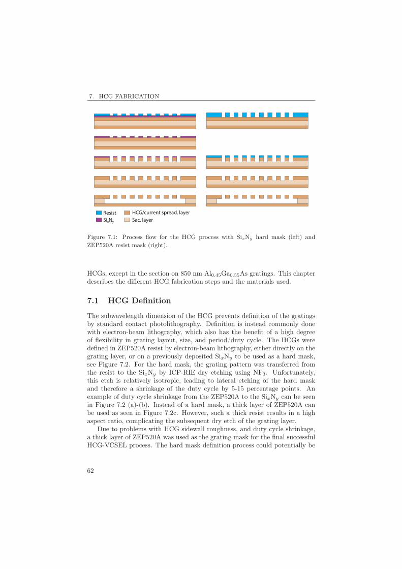
7. HCG FABRICATION
Resist HCG/current spread. layerSac. layerSixNy
Figure 7.1: Process flow for the HCG process with SixNy hard mask (left) andZEP520A resist mask (right).
HCGs, except in the section on 850 nm Al0.45Ga0.55As gratings. This chapterdescribes the different HCG fabrication steps and the materials used.
7.1 HCG Definition
The subwavelength dimension of the HCG prevents definition of the gratingsby standard contact photolithography. Definition is instead commonly donewith electron-beam lithography, which also has the benefit of a high degreeof flexibility in grating layout, size, and period/duty cycle. The HCGs weredefined in ZEP520A resist by electron-beam lithography, either directly on thegrating layer, or on a previously deposited SixNy to be used as a hard mask,see Figure 7.2. For the hard mask, the grating pattern was transferred fromthe resist to the SixNy by ICP-RIE dry etching using NF3. Unfortunately,this etch is relatively isotropic, leading to lateral etching of the hard maskand therefore a shrinkage of the duty cycle by 5-15 percentage points. Anexample of duty cycle shrinkage from the ZEP520A to the SixNy can be seenin Figure 7.2 (a)-(b). Instead of a hard mask, a thick layer of ZEP520A canbe used as seen in Figure 7.2c. However, such a thick resist results in a highaspect ratio, complicating the subsequent dry etch of the grating layer.
Due to problems with HCG sidewall roughness, and duty cycle shrinkage,a thick layer of ZEP520A was used as the grating mask for the final successfulHCG-VCSEL process. The hard mask definition process could potentially be
62
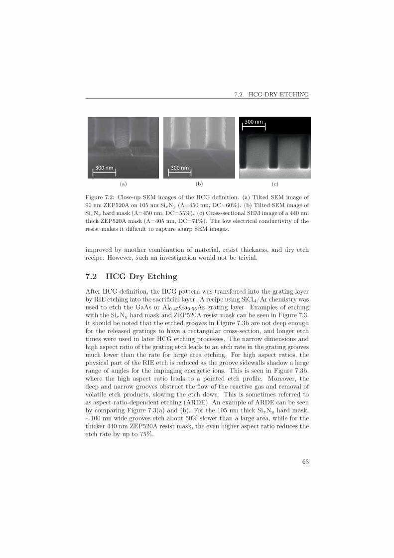
7.2. HCG DRY ETCHING
300 nm
(a)
300 nm
(b)
300 nm
(c)
Figure 7.2: Close-up SEM images of the HCG definition. (a) Tilted SEM image of90 nm ZEP520A on 105 nm SixNy (Λ=450 nm, DC=60%). (b) Tilted SEM image ofSixNy hard mask (Λ=450 nm, DC=55%). (c) Cross-sectional SEM image of a 440 nmthick ZEP520A mask (Λ=405 nm, DC=71%). The low electrical conductivity of theresist makes it difficult to capture sharp SEM images.
improved by another combination of material, resist thickness, and dry etchrecipe. However, such an investigation would not be trivial.
7.2 HCG Dry Etching
After HCG definition, the HCG pattern was transferred into the grating layerby RIE etching into the sacrificial layer. A recipe using SiCl4/Ar chemistry wasused to etch the GaAs or Al0.45Ga0.55As grating layer. Examples of etchingwith the SixNy hard mask and ZEP520A resist mask can be seen in Figure 7.3.It should be noted that the etched grooves in Figure 7.3b are not deep enoughfor the released gratings to have a rectangular cross-section, and longer etchtimes were used in later HCG etching processes. The narrow dimensions andhigh aspect ratio of the grating etch leads to an etch rate in the grating groovesmuch lower than the rate for large area etching. For high aspect ratios, thephysical part of the RIE etch is reduced as the groove sidewalls shadow a largerange of angles for the impinging energetic ions. This is seen in Figure 7.3b,where the high aspect ratio leads to a pointed etch profile. Moreover, thedeep and narrow grooves obstruct the flow of the reactive gas and removal ofvolatile etch products, slowing the etch down. This is sometimes referred toas aspect-ratio-dependent etching (ARDE). An example of ARDE can be seenby comparing Figure 7.3(a) and (b). For the 105 nm thick SixNy hard mask,∼100 nm wide grooves etch about 50% slower than a large area, while for thethicker 440 nm ZEP520A resist mask, the even higher aspect ratio reduces theetch rate by up to 75%.
63
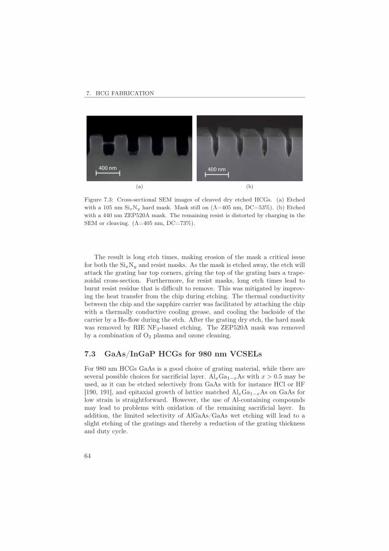
7. HCG FABRICATION
400 nm
(a)
400 nm
(b)
Figure 7.3: Cross-sectional SEM images of cleaved dry etched HCGs. (a) Etchedwith a 105 nm SixNy hard mask. Mask still on (Λ=405 nm, DC=53%). (b) Etchedwith a 440 nm ZEP520A mask. The remaining resist is distorted by charging in theSEM or cleaving. (Λ=405 nm, DC=73%).
The result is long etch times, making erosion of the mask a critical issuefor both the SixNy and resist masks. As the mask is etched away, the etch willattack the grating bar top corners, giving the top of the grating bars a trape-zoidal cross-section. Furthermore, for resist masks, long etch times lead toburnt resist residue that is difficult to remove. This was mitigated by improv-ing the heat transfer from the chip during etching. The thermal conductivitybetween the chip and the sapphire carrier was facilitated by attaching the chipwith a thermally conductive cooling grease, and cooling the backside of thecarrier by a He-flow during the etch. After the grating dry etch, the hard maskwas removed by RIE NF3-based etching. The ZEP520A mask was removedby a combination of O2 plasma and ozone cleaning.
7.3 GaAs/InGaP HCGs for 980 nm VCSELs
For 980 nm HCGs GaAs is a good choice of grating material, while there areseveral possible choices for sacrificial layer. AlxGa1−xAs with x > 0.5 may beused, as it can be etched selectively from GaAs with for instance HCl or HF[190, 191], and epitaxial growth of lattice matched AlxGa1−xAs on GaAs forlow strain is straightforward. However, the use of Al-containing compoundsmay lead to problems with oxidation of the remaining sacrificial layer. Inaddition, the limited selectivity of AlGaAs/GaAs wet etching will lead to aslight etching of the gratings and thereby a reduction of the grating thicknessand duty cycle.
64
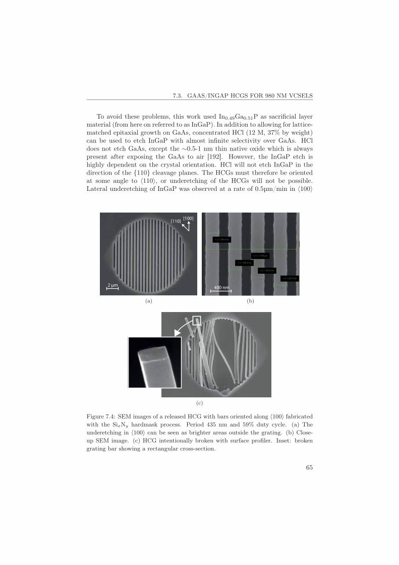
7.3. GAAS/INGAP HCGS FOR 980 NM VCSELS
To avoid these problems, this work used In0.49Ga0.51P as sacrificial layermaterial (from here on referred to as InGaP). In addition to allowing for lattice-matched epitaxial growth on GaAs, concentrated HCl (12 M, 37% by weight)can be used to etch InGaP with almost infinite selectivity over GaAs. HCldoes not etch GaAs, except the ∼0.5-1 nm thin native oxide which is alwayspresent after exposing the GaAs to air [192]. However, the InGaP etch ishighly dependent on the crystal orientation. HCl will not etch InGaP in thedirection of the {110} cleavage planes. The HCGs must therefore be orientedat some angle to 〈110〉, or underetching of the HCGs will not be possible.Lateral underetching of InGaP was observed at a rate of 0.5μm/min in 〈100〉
2 μm
[110] [100]
(a)
400 nm
(b)
(c)
Figure 7.4: SEM images of a released HCG with bars oriented along 〈100〉 fabricatedwith the SixNy hardmask process. Period 435 nm and 59% duty cycle. (a) Theunderetching in 〈100〉 can be seen as brighter areas outside the grating. (b) Close-up SEM image. (c) HCG intentionally broken with surface profiler. Inset: brokengrating bar showing a rectangular cross-section.
65
7. HCG FABRICATION
(45° angle to the 110 cleavage planes), making etch times of 2-3 min sufficientfor the HCG underetch. The crystallographic dependence was found to be ingood agreement with [193]. Alternatively, the similar compound InxAl1−xPcould have been used as sacrificial layer, as demonstrated by Ansæk et al. forGaAs gratings in tunable 1060 nm MEMS HCG-VCSELs [185, 194].
No buckling of the bars of released GaAs gratings were observed, indicat-ing low strain in the GaAs grating layer. Previously realized HCG-VCSELsoften use stress-relieving trenches around the gratings [164], but we did notfind this necessary. The underetching of the gratings can be directly confirmedby breaking the grating bars with a surface profiler. This enables direct ob-servation of the semiconductor-air interface below the grating, and, with a bitof luck, the HCG cross-section can also be studied, as seen in Figure 7.4c.
7.4 AlGaAs/GaAs HCGs for 850 nm VCSELs
Our HCG-VCSEL efforts initially focused on 850 nm devices with gratingsof Al0.45Ga0.55As with a GaAs sacrificial layer. No successful 850 nm HCG-VCSELs were fabricated due to problems with the grating etch described inthe next section. By the time these problems were resolved, the Al0.45Ga0.55Asgratings for 850 nm VCSELs had already been put aside in favor of the GaAsgratings for 980 nm VCSELs. The development of the HCG process is never-theless presented here, since it could potentially be applied to fabricate 850 nmHCG-VCSELs. This is the only section where 850 nm Al0.45Ga0.55As/GaAsHCGs are discussed.
Successful underetching and release of HCGs were first achieved by sacri-ficial layer etching with H2O2:NH4OH=1:50 diluted with 5 parts water. How-ever, the etchant was found to severely oxidize the Al0.45Ga0.55As grating. Thegratings were therefore underetched using the citric acid mixture described in[186], and used in for instance [164]. First, citric acid was mixed as anhydrouscitric acid and water at a ratio of 1:1 by weight, and the pH value was adjustedto 6.5 with NH4OH for high selectivity to AlGaAs [195]. It was then diluted as(citric acid mixture):H2O2=5:1 to further improve selectivity [196], and heatedto 60°C. A slight anisotropy was observed with twice as fast underetch in 〈100〉compared to 〈110〉.
A selectivity of around 250 to Al0.45Ga0.55As was observed in good agree-ment with [197]. Even though this is a rather high selectivity it still has tobe taken into consideration as the HCG properties are highly sensitive to thegrating thickness. Assuming that an underetch of 1 μm is desired in 〈110〉,means that GaAs in 〈100〉 (vertical direction on our wafer) will etch 2 μm.With a selectivity of 250, the Al0.45Ga0.55As grating will etch 8 nm on thetop surface, and a bit less on the underside while the sacrificial layer is etchedaway. In total, the grating will be thinned by 10-15 nm during the release
66
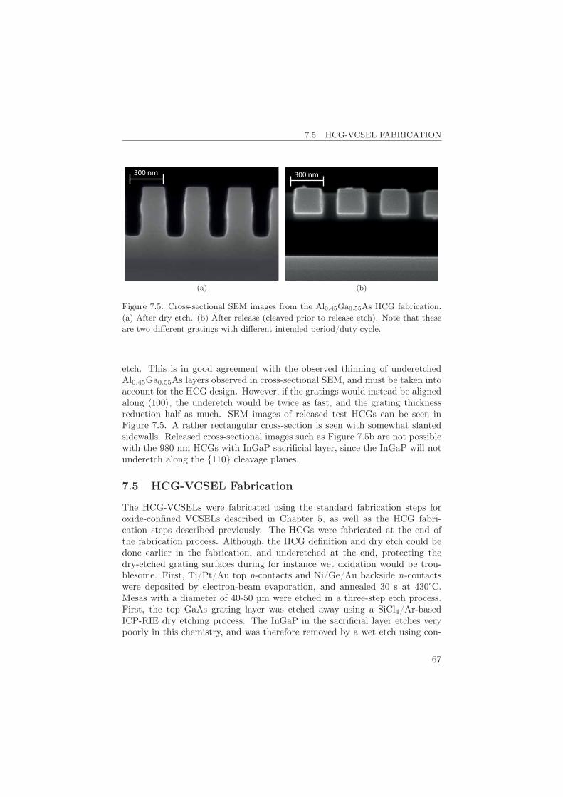
7.5. HCG-VCSEL FABRICATION
300 nm
(a)
300 nm
(b)
Figure 7.5: Cross-sectional SEM images from the Al0.45Ga0.55As HCG fabrication.(a) After dry etch. (b) After release (cleaved prior to release etch). Note that theseare two different gratings with different intended period/duty cycle.
etch. This is in good agreement with the observed thinning of underetchedAl0.45Ga0.55As layers observed in cross-sectional SEM, and must be taken intoaccount for the HCG design. However, if the gratings would instead be alignedalong 〈100〉, the underetch would be twice as fast, and the grating thicknessreduction half as much. SEM images of released test HCGs can be seen inFigure 7.5. A rather rectangular cross-section is seen with somewhat slantedsidewalls. Released cross-sectional images such as Figure 7.5b are not possiblewith the 980 nm HCGs with InGaP sacrificial layer, since the InGaP will notunderetch along the {110} cleavage planes.
7.5 HCG-VCSEL Fabrication
The HCG-VCSELs were fabricated using the standard fabrication steps foroxide-confined VCSELs described in Chapter 5, as well as the HCG fabri-cation steps described previously. The HCGs were fabricated at the end ofthe fabrication process. Although, the HCG definition and dry etch could bedone earlier in the fabrication, and underetched at the end, protecting thedry-etched grating surfaces during for instance wet oxidation would be trou-blesome. First, Ti/Pt/Au top p-contacts and Ni/Ge/Au backside n-contactswere deposited by electron-beam evaporation, and annealed 30 s at 430°C.Mesas with a diameter of 40-50 μm were etched in a three-step etch process.First, the top GaAs grating layer was etched away using a SiCl4/Ar-basedICP-RIE dry etching process. The InGaP in the sacrificial layer etches verypoorly in this chemistry, and was therefore removed by a wet etch using con-
67
7. HCG FABRICATION
centrated HCl. This step will underetch the mesa edges around 1 μm, but thisis of no concern for the large mesas used. Finally, the ICP-RIE dry etch wasused to etch partly into the n-DBR to expose the layers to be oxidized. Thecurrent apertures were formed by selective wet oxidation of one 30-nm-thickAl0.98Ga0.02As layer on each side of the QWs. Prior to planarization withBCB, a SixNy layer was deposited by PECVD to enhance the BCB adhesion.The BCB on top of the mesas was removed in a photolithography step, usingthe BCB as a negative photoresist. A short ICP-RIE dry etch with CF4/O2
made sure the BCB was completely removed from the mesa. The remainingSixNy on the mesa was removed by NF3 RIE etching before Ti/Au bondpadswere deposited.
Throughout most of the fabrication, the top surface was protected by alayer of sputtered SixNy in order to avoid contamination or unintentionaletching. Each resist removal was performed using a combination of standardsolvents, O2 plasma ashing, and ozone cleaning. Especially ozone cleaningwas found to be of vital importance, as the mesa surface must be absolutelyclean before the HCG fabrication starts. Without the ozone clean, the HCGwet etch only worked a fraction of the attempts. Surprisingly, this problemwas never observed when processing test HCGs on blank chips with no priorprocessing steps performed. The conclusion must be that even with thoroughresist removal with solvents and O2 plasma ashing, there are some residue leftthat does not hinder the HCG dry etch, but later obstructs the wet etch ofthe InGaP. The short 10 minute ozone cleaning likely forms an oxide layer onthe GaAs grating layer which is thinner than one nanometer [198], which isremoved in the final HCG wet etch.
After the bondpad deposition, and thorough cleaning of the mesa surface,the HCGs were fabricated using the ZEP520A etch mask as previously de-scribed. Full HCG-VCSEL structures were also fabricated using the SixNy
hard mask process, but no clear lasing was observed. Using only the re-sist mask seems to yield smoother grating sidewalls with a more rectangularcross-section, and thereby higher-reflective gratings. No successful 850 nmHCG-VCSELs with Al0.45Ga0.55As gratings and GaAs sacrificial layer wereprocessed because of the mentioned etch problems, that were later solved bythe ozone cleaning. Once the problem had been solved, the project had alreadymoved on to the 980 nm HCG-VCSELs.
68
Chapter 8
HCG-VCSEL Experiments
The main experimental results for multi-wavelength HCG-VCSEL arrays canbe found in Paper H, while this chapter presents results from reflection mea-surements on test HCGs, and some additional characteristics of the HCG-VCSELs. Note that only 980 nm GaAs HCGs are characterized.
8.1 Test Structures
Prior to integration of HCGs on full VCSEL structures, test structures con-sisting of only the grating and sacrificial layers were processed as part of thedevelopment of the HCG fabrication process. The epitaxial structure wasgrown by MOCVD on 2" (001)-GaAs wafers at the Royal Institute of Tech-nology in Stockholm, Sweden. A 285 nm thick grating layer was grown on topof a 520 nm In0.49Ga0.51P sacrificial layer. Both layers were p-doped to about1 · 1019 cm−3. HCGs with periods of 435-475 nm and duty cycles 35-65% werefabricated using the SixNy hard mask process (see Chapter 7). SEM imagesof the fabricated HCGs can be seen in Figure 7.4.
The reflectivity of the HCGs was investigated using a micro-reflectivitymeasurement setup at HP Labs in Palo Alto, CA, USA. Light from a fiber-coupled superluminescent diode, with a useful spectral width of around 100 nmat 1040 nm, was focused on the HCG using a lens setup, resulting in a spot sizeof 5 μm. The reflected light was then collected back into the single-mode fiberby the same lens setup, and connected to an optical spectrum analyzer (OSA)through a 3dB fiber coupler. The measurement was calibrated against electron-beam evaporated gold next to the HCGs, assuming a reflectivity of 98% forthe gold throughout the entire wavelength range [199]. Due to chromaticabberations in the lens package, its height had to be changed to maintain
69
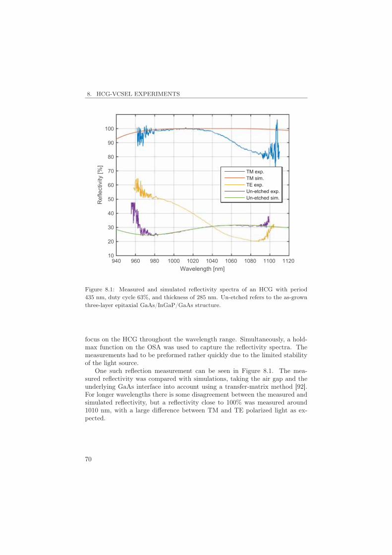
8. HCG-VCSEL EXPERIMENTS
Wavelength [nm]940 960 980 1000 1020 1040 1060 1080 1100 1120
Ref
lect
ivity
[%]
10
20
30
40
50
60
70
80
90
100
TM exp.TM sim.TE exp.Un-etched exp.Un-etched sim.
Figure 8.1: Measured and simulated reflectivity spectra of an HCG with period435 nm, duty cycle 63%, and thickness of 285 nm. Un-etched refers to the as-grownthree-layer epitaxial GaAs/InGaP/GaAs structure.
focus on the HCG throughout the wavelength range. Simultaneously, a hold-max function on the OSA was used to capture the reflectivity spectra. Themeasurements had to be preformed rather quickly due to the limited stabilityof the light source.
One such reflection measurement can be seen in Figure 8.1. The mea-sured reflectivity was compared with simulations, taking the air gap and theunderlying GaAs interface into account using a transfer-matrix method [92].For longer wavelengths there is some disagreement between the measured andsimulated reflectivity, but a reflectivity close to 100% was measured around1010 nm, with a large difference between TM and TE polarized light as ex-pected.
70
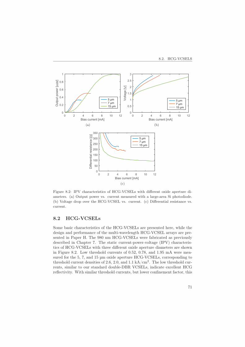
8.2. HCG-VCSELS
Bias current [mA]0 2 4 6 8 10 12
Out
put p
ower
[ mW
]
0
0.2
0.4
0.6
0.8
1
5 7 15
(a)
Bias current [mA]0 2 4 6 8 10 12
Vol
tage
[ V]
0
0.5
1
1.5
2
2.5
3
5 7 15
(b)
Bias current [mA]0 2 4 6 8 10 12
Diff
eren
tial r
esis
tanc
e [
]
0
50
100
150
200
250
300
350
5 7 15
(c)
Figure 8.2: IPV characteristics of HCG-VCSELs with different oxide aperture di-ameters. (a) Output power vs. current measured with a large-area Si photodiode.(b) Voltage drop over the HCG-VCSEL vs. current. (c) Differential resistance vs.current.
8.2 HCG-VCSELs
Some basic characteristics of the HCG-VCSELs are presented here, while thedesign and performance of the multi-wavelength HCG-VCSEL arrays are pre-sented in Paper H. The 980 nm HCG-VCSELs were fabricated as previouslydescribed in Chapter 7. The static current-power-voltage (IPV) characteris-tics of HCG-VCSELs with three different oxide aperture diameters are shownin Figure 8.2. Low threshold currents of 0.52, 0.78, and 1.95 mA were mea-sured for the 5, 7, and 15 μm oxide aperture HCG-VCSELs, corresponding tothreshold current densities of 2.6, 2.0, and 1.1 kA/cm2. The low threshold cur-rents, similar to our standard double-DBR VCSELs, indicate excellent HCGreflectivity. With similar threshold currents, but lower confinement factor, this
71
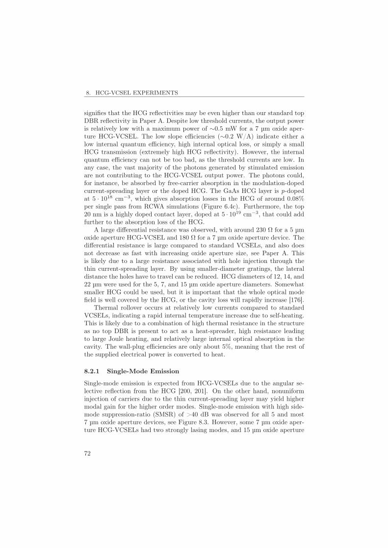
8. HCG-VCSEL EXPERIMENTS
signifies that the HCG reflectivities may be even higher than our standard topDBR reflectivity in Paper A. Despite low threshold currents, the output poweris relatively low with a maximum power of ∼0.5 mW for a 7 μm oxide aper-ture HCG-VCSEL. The low slope efficiencies (∼0.2 W/A) indicate either alow internal quantum efficiency, high internal optical loss, or simply a smallHCG transmission (extremely high HCG reflectivity). However, the internalquantum efficiency can not be too bad, as the threshold currents are low. Inany case, the vast majority of the photons generated by stimulated emissionare not contributing to the HCG-VCSEL output power. The photons could,for instance, be absorbed by free-carrier absorption in the modulation-dopedcurrent-spreading layer or the doped HCG. The GaAs HCG layer is p-dopedat 5 · 1018 cm−3, which gives absorption losses in the HCG of around 0.08%per single pass from RCWA simulations (Figure 6.4c). Furthermore, the top20 nm is a highly doped contact layer, doped at 5 · 1019 cm−3, that could addfurther to the absorption loss of the HCG.
A large differential resistance was observed, with around 230 Ω for a 5 μmoxide aperture HCG-VCSEL and 180 Ω for a 7 μm oxide aperture device. Thedifferential resistance is large compared to standard VCSELs, and also doesnot decrease as fast with increasing oxide aperture size, see Paper A. Thisis likely due to a large resistance associated with hole injection through thethin current-spreading layer. By using smaller-diameter gratings, the lateraldistance the holes have to travel can be reduced. HCG diameters of 12, 14, and22 μm were used for the 5, 7, and 15 μm oxide aperture diameters. Somewhatsmaller HCG could be used, but it is important that the whole optical modefield is well covered by the HCG, or the cavity loss will rapidly increase [176].
Thermal rollover occurs at relatively low currents compared to standardVCSELs, indicating a rapid internal temperature increase due to self-heating.This is likely due to a combination of high thermal resistance in the structureas no top DBR is present to act as a heat-spreader, high resistance leadingto large Joule heating, and relatively large internal optical absorption in thecavity. The wall-plug efficiencies are only about 5%, meaning that the rest ofthe supplied electrical power is converted to heat.
8.2.1 Single-Mode Emission
Single-mode emission is expected from HCG-VCSELs due to the angular se-lective reflection from the HCG [200, 201]. On the other hand, nonuniforminjection of carriers due to the thin current-spreading layer may yield highermodal gain for the higher order modes. Single-mode emission with high side-mode suppression-ratio (SMSR) of >40 dB was observed for all 5 and most7 μm oxide aperture devices, see Figure 8.3. However, some 7 μm oxide aper-ture HCG-VCSELs had two strongly lasing modes, and 15 μm oxide aperture
72
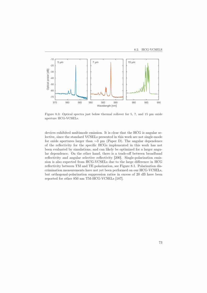
8.2. HCG-VCSELS
975 980 985
Opt
ical
pow
er [d
B]
-70
-60
-50
-40
-30
-20
-105 μm 7 μm 15 μm
Wavelength [nm]980 985 990 980 985 990
Figure 8.3: Optical spectra just below thermal rollover for 5, 7, and 15 μm oxideaperture HCG-VCSELs.
devices exhibited multimode emission. It is clear that the HCG is angular se-lective, since the standard VCSELs presented in this work are not single-modefor oxide apertures larger than ∼3 μm (Paper D). The angular dependenceof the reflectivity for the specific HCGs implemented in this work has notbeen evaluated by simulations, and can likely be optimized for a larger angu-lar dependence. On the other hand, there is a trade-off between broadbandreflectivity and angular selective reflectivity [200]. Single-polarization emis-sion is also expected from HCG-VCSELs due to the large difference in HCGreflectivity between TM and TE polarization, see Figure 8.1. Polarization dis-crimination measurements have not yet been performed on our HCG-VCSELs,but orthogonal-polarization suppression ratios in excess of 20 dB have beenreported for other 850 nm TM-HCG-VCSELs [187].
73

74
Chapter 9
Outlook and Future Directions
It is clear that future optical interconnects will require a continuous improve-ment of high-speed VCSEL performance. This thesis and its appended papersaim at dissecting some important aspects, but there are many topics outside ofthe scope of this thesis. This chapter discusses some possible future directionsfor continued research.
Future optical interconnects for extremely high capacity (many Tbit/s) willlikely use combination of high-speed VCSELs and photodetectors, advanceddriver and receiver circuits with equalization [45], multilevel modulation for-mats [39], and multiplexing (e.g. ribbons of multicore fiber [79, 202] and/orWDM [62]). However, it is important to simultaneously strive for low powerconsumption, small footprint, and, as always, low cost. A further miniaturiza-tion by integration of III-V VCSELs on silicon is another important path,which could enable photonic integrated circuits with heterogeneously inte-grated VCSELs [171, 203], drivers, and silicon nitride waveguides [204], aswell as other elements such as MUX/DEMUX for WDM [205].
Increasing the bandwidth of VCSELs (and photodiodes) continues to bean important path towards higher-speed optical interconnects. Even thoughadvanced electronic compensation techniques will likely be used to boost thedata rate [43–45], a high device bandwidth will simplify the driver and receivercircuit design, reducing their energy consumption and footprint. State-of-the-art high-speed VCSELs have very high intrinsic bandwidths, but are restrainedby parasitics and thermal effects (see Section 3.4 and Paper A). Special atten-tion should be paid to device resistance since it impacts both the parasiticsand the self-heating. Thermal effects may be improved by moving from 850to 1060 nm, due to higher differential gain [29], deeper QWs for lower carrierleakage [100], the use of binary GaAs for improved thermal conductivity [117],
75
9. OUTLOOK AND FUTURE DIRECTIONS
and the possibility of bottom emitting devices for flip-chip mounting [30].Longer-reach MMF links (>500 m) might not become economically vi-
able, depending on the future cost of MMF and SMF, and the transceivers.However, an introduction of WDM could tip the balance in favor for MMF.Anyway, quasi-single-mode VCSELs will still be needed to increase the datarate of links up to 500 m to ≥25 Gbit/s. Since the next standard data rate after25 Gbit/s is expected to be 40 Gbit/s, a logical next step would be to pursuequasi-single-mode VCSELs capable of transmitting 40 Gbit/s over 500 m ofMMF. This could be accomplished by simultaneous optimization of the spec-tral and dynamic properties. In a mode-filter VCSEL this requires a highertotal top mirror loss, while keeping the modal discrimination large. This couldbe achieved by using fewer mirror pairs (equivalent to moving further to theright in Figure 4.2b). Longer-reach optical interconnects would also benefitfrom longer wavelengths due to the reduced loss and chromatic dispersion inthe silica used in MMFs [74].
After more than three years of work, the fact that air-coupled-cavity HCG-VCSELs could achieve lasing with low threshold currents was rather surprisingto me. Lasing devices were only recently realized (July 2015), and more de-tailed measurements and analyses (of for instance thermal properties) couldnot be performed in time for this thesis. However, the performance can prob-ably be significantly improved by considering the following points:
• Larger wavelength span: Successful fabrication of HCGs with duty cyclescovering the full span of 40-85% would enable an even larger span of reso-nance wavelengths. However, simultaneous dry etching of HCGs with sig-nificantly different aspect ratios is not trivial due to aspect ratio dependentetching. Ultimately, the achievable lasing span for any multi-wavelengthVCSEL array is limited by the gain bandwidth of the QWs, which will alsolead to a variation in device performance across the array (e.g. thresholdcurrent, output power, and differential gain).
• Higher output power: Despite low threshold currents the output poweris rather low. One reason could simply be that the HCG transmission istoo low, leading to a large internal absorption and low slope efficiency. Ifthis is the case, bottom emitting devices could be designed, with ∼100%-reflective undoped HCGs top mirrors. Another concern is the HCG losspredicted by RCWA simulations, induced by free-carrier absorption due todoping. Experimental verification by evaluation of an undoped HCG wouldtherefore be interesting. A third obvious critical issue is the early thermalrollover of the HCG-VCSELs. Future designs would need to pay significantattention to heat-sinking and thermal conductivity.
• High-speed design: A high-speed design of any WDM VCSEL arraywould involve trade-offs between the static and dynamic properties. How-
76
ever, HCGs are at an advantage since the wavelength and top-mirror reflec-tivity can be varied independent of each other in a single process step, whichis not possible with any other technique (Section 6.1). For instance, a uni-form threshold current could be achieved by tailoring the HCG reflectivityto compensate for the spectral variation of the QW gain.
Whether HCG-VCSELs are the most suitable technique to realize monolithically-integrated WDM arrays remains uncertain, due to the complicated fabricationand the relatively low efficiencies so far presented for HCG-VCSELs [164, 166,187, 194]. It is in fact unclear whether any of the monolithic multi-wavelengthVCSEL techniques, presented in Section 6.1, have the capability of high-speedmodulation over a sufficiently wide wavelength span for practical use in un-cooled optical interconnects. The industry is therefore currently exploringcoarse WDM using discreet VCSELs fabricated from different wafers [75, 85].However, this demonstrates a real need for multi-wavelength VCSEL arrays,motivating continued research towards wide-span high-speed monolithic multi-wavelength VCSEL arrays.
77

78
Chapter 10
Summary of Papers
Paper A
“High-speed VCSELs with strong confinement of optical fields andcarriers,” to appear in J. of Lightwave Technol., vol. 33, no. 24, pp. 1-9,Dec. 2015, (invited paper).
This invited paper presents the design, fabrication, and performance of a newgeneration of 850 nm high-speed VCSELs, where both carriers and opticalfields are strongly confined to the active region. A short 1/2-λ cavity providesa large longitudinal optical confinement. The strong lateral confinement ofcarriers was obtained by positioning the oxide layers close to the QWs, yield-ing high internal quantum efficiencies, low threshold currents, and high WPEsof up to 34% for 7.5 μm oxide aperture VCSELs at RT and 24% at 85°C. Ananalysis of the temperature-dependent small-signal modulation response indi-cates that the bandwidth is limited by parasitics at RT, and by a combinationof parasitics and thermal effects at 85°C.
My contribution: I participated in the design work, fabricated the VCSELs,performed all the measurements, and analyzed the results. I wrote the paperand presented the results at the European Conference on Lasers and Electro-Optics 2015 (Munich, Germany).
79
10. SUMMARY OF PAPERS
Paper B
“30 GHz bandwidth 850 nm VCSEL with sub-100 fJ/bit energy dis-sipation at 25-50 Gbit/s,” Electron. Lett., vol. 51, no. 14, pp. 1096-1098,July 2015.
In this paper we present results from data transmission experiments using theVCSEL design presented in Paper A. A record-high modulation bandwidthof 30 GHz is demonstrated for a small-oxide-aperture VCSEL. High internalquantum efficiency and low threshold currents contributed to a high D-factorof 17.5 GHz/mA1/2, and a bandwidth of 25 GHz already at a bias currentof 1.8 mA. This enabled error-free (BER <10−12) energy-efficient high-speeddata transmission at 40 and 50 Gbit/s, with record-low dissipated energy inthe VCSEL of 73 and 95 fJ/bit, respectively.
My contribution: I fabricated the VCSELs, identified energy-efficient high-speed data transmission as a promising application, performed all the mea-surements, and analyzed the results. I wrote the paper and presented theresults at the European Conference on Lasers and Electro-Optics 2015 (Mu-nich, Germany).
Paper C
“20 Gbit/s error-free operation of 850 nm oxide-confined VCSELsbeyond 1 km of multimode fibre,” Electron. Lett., vol. 48, no. 19, pp. 1225-1227, Sept. 2012.
In this paper we present long-reach transmission using a small-oxide aperture(∼3 μm) quasi-single-mode VCSEL. A narrow RMS spectral width of 0.29 nmreduced the effect of chromatic dispersion in the MMF. This enabled error-free(BER <10−12) transmission at 20 Gbit/s over 1.1 km, which was at that timea record bit-rate-distance product for directly-modulated VCSEL MMF links.
My contribution: I helped introduce R. Safaisini to the VCSEL fabricationprocess and assisted with the fabrication, measurements, and analysis. I alsopresented the result at the European VCSEL Day 2013 (Lausanne, Switzer-land).
Paper D
“High-Speed 850 nm Quasi-Single-Mode VCSELs for Extended-ReachOptical Interconnects,” J. Opt. Commun. Netw., vol. 5, no. 7, pp. 686-695,July 2013.
80
This paper is an expanded investigation of the quasi-single-mode VCSELs inPaper C, with a detailed discussion on the design and fabrication. The VC-SEL dynamic properties were investigated by small-signal modulation mea-surements, demonstrating a bandwidth of 23 GHz and a large D-factor of17.3 GHz/mA1/2. A 10 GHz photoreceiver with an integrated transimpedanceamplifier was used to demonstrate data transmission at 22 Gbit/s over 1100 mof OM4 MMF. A theoretical study of the influence of the receiver bandwidthon the link performance showed that a receiver with 15 GHz bandwidth shouldenable transmission at 25 Gbit/s over 1000 m. In addition, 2 km transmis-sion at 20 Gbit/s could be possible with a receiver with >15 GHz bandwidth,but this also requires sufficient VCSEL output power to overcome fiber andconnector losses.
My contribution: I aided R. Safaisini with the VCSEL fabrication process,and assisted with the measurements and analysis.
Paper E
“25 Gbit/s transmission over 500 m multimode fibre using 850 nmVCSEL with integrated mode filter,” Electron. Lett., vol. 48, no. 9,pp. 517-518, April 2012.
The spectral width of high-speed VCSELs developed at Chalmers was reducedby integrating a surface-relief mode filter on the VCSEL surface. This enablesVCSEL with narrow spectral width with larger oxide aperture than in Papers Cand D. A significant reduction in RMS spectral width from 0.9 to 0.3 nm wasobtained when etching a 1.5 μm diameter mode filter on a 5 μm oxide apertureVCSEL. A transmission distance of 500 m was achieved at 25 Gbit/s.
My contribution: I established the mode filter fabrication process and fab-ricated the VCSELs. I performed all the measurements, analyzed the results,wrote the paper, and presented the results at SPIE Photonics West 2012 (SanFrancisco, CA, USA).
Paper F
“Reducing the spectral width of high speed oxide confined VCSELsusing an integrated mode filter,” Proc. of SPIE, vol. 8276, pp. 82760L1-8,Feb. 2012.
This conference paper is an expanded study on the mode filter VCSELs fromPaper E with more details on device structure and mode filter functional-ity. Spectrally resolved near-field imaging was used to identify the different
81
10. SUMMARY OF PAPERS
transverse modes and their relative radial intensity distributions of a large-spectral-width high-speed VCSEL. The static and dynamic properties of threedifferent 5 μm-aperture VCSELs are compared; one with a surface-relief modefilter, one without any surface etch (full anti-phase top DBR reflection), andone device with the entire surface etched to an in-phase reflection. As ex-pected, the shallow surface etching has a significant influence on both staticand dynamic properties.
My contribution: I fabricated the VCSELs, performed all the measurements,and analyzed the results. I wrote the paper and presented it at SPIE PhotonicsWest 2012 (San Francisco, CA, USA).
Paper G
“20 Gb/s data transmission over 2 km multimode fibre using 850 nmmode filter VCSELs,” Electron. Lett., vol. 50, no. 1, pp. 40-42, Jan. 2014.,Aug. 2013.
This paper present a new generation of mode-filter VCSELs with improvedmode filter fabrication process. By using a 6 μm oxide aperture VCSEL witha 3 μm surface-relief mode filter, single-mode output powers exceeding 4 mWwas achieved for high-speed VCSELs. This enabled error-free (BER < 10−12)transmission at 25 and 20 Gbit/s over 1300 and 2000 m of OM4 MMF, respec-tively. The resulting bit-rate-distance product of 40 Gbit·km/s is the highestever reported for a directly-modulated OOK 850 nm VCSEL link.
My contribution: I fabricated the VCSELs together with R. Safaisini. Inparticular I performed the mode-filter fabrication process. I assisted with themeasurements and analysis of the results. I co-authored the paper and wasthe corresponding author.
Paper H
“Demonstration of post-growth wavelength setting of VCSELs usinghigh-contrast gratings,” submitted to Optics Express, Aug. 2015.
This paper demonstrates experimentally, for the first time, post-growth wave-length setting of electrically-injected VCSELs by varying the parameters ofhigh-contrast gratings (HCGs). The design, fabrication, and static propertiesof multi-wavelength HCG-VCSEL arrays are presented. As the HCG reflec-tion phase varies significantly with grating period and duty cycle, an HCG topmirror can set the VCSEL wavelength depending on its parameters. A cav-ity design for maximum wavelength setting range was used, requiring HCGs
82
with very high reflectivity. The air-suspended GaAs HCGs were realized byselectively removing a InGaP sacrificial layer. Lasing was observed over awavelength span of 15 nm, starting at 977 nm. Sub-mA thresholds indicateexcellent HCG reflectivity.
My contribution: I participated in the design work and developed the HCGfabrication process. I fabricated the HCG-VCSELs, performed all the mea-surements, and wrote the paper.
83

84
References
[1] J. A. Kash, A. Benner, F. E. Doany, D. Kuchta, B. G. Lee, P. Pepelju-goski, L. Schares, C. Schow, and M. Taubenblatt, “Optical interconnectsin future servers,” in Optical Fiber Communication Conference/NationalFiber Optic Engineers Conference 2011, p. OWQ1, Optical Society ofAmerica, 2011.
[2] “Top #1 systems.” http://www.top500.org/featured/top-systems/
, accessed 2015-08-14, 2015.
[3] N. Lehrer, “The largest data centers in the world.” http:
//www.networkcomputing.com/cloud-infrastructure/the-
largest-data-centers-in-the-world/d/d-id/1269250 , accessed2015-08-16, 2014.
[4] Féderation Internationalde de Football Association (FIFA), “Laws of thegame,” 2015/2016.
[5] A. Flatman, “Data centre link lengths.” http://www.ieee802.org/3/
NGBASET/public/nov12/flatman_01a_1112_ngbt.pdf , accessed 2015-08-17, 2012.
[6] H. Liu, C. F. Lam, and C. Johnson, “Scaling optical interconnects indatacenter networks opportunities and challenges for WDM,” in HighPerformance Interconnects (HOTI), 2010 IEEE 18th Annual Symposiumon, pp. 113–116, 2010.
[7] J. Kash, A. Benner, F. Doany, D. Kuchta, B. Lee, P. Pepeljugoski,L. Schares, C. Schow, and M. Taubenblatt, “Optical interconnects inexascale supercomputers,” in 23rd Annual Meeting of the IEEE Photon-ics Society, pp. 483–484, Nov 2010.
[8] A. Krishnamoorthy, K. Goossen, W. Jan, X. Zheng, R. Ho, G. Li,R. Rozier, F. Liu, D. Patil, J. Lexau, H. Schwetman, D. Feng, M. As-ghari, T. Pinguet, and J. Cunningham, “Progress in low-power switched
85
REFERENCES
optical interconnects,” IEEE J. Sel. Top. Quantum Electron., vol. 17,pp. 357–376, March 2011.
[9] “Obama orders speedy delivery of first exascale supercomputer.” http:
//spectrum.ieee.org/tech-talk/computing/hardware/obama-
orders-speedy-delivery-of-first-exascale-supercomputer- ,accessed 2015-08-14, 2015.
[10] A. Larsson, “Advances in VCSELs for communication and sensing,”IEEE J. Sel. Top. Quantum Electron., vol. 17, no. 6, pp. 1552–1567,2011.
[11] R. W. Herrick, Materials and Reliability Handbook for SemiconductorOptical and Electron Devices. Springer Science+Business Media, 2013.
[12] R. E. Freund, C. Bunge, N. N. Ledentsov, D. Molin, and C. Cas-par, “High-speed transmission in multimode fibers,” J. Lightw. Technol.,vol. 28, no. 4, pp. 569–586, 2010.
[13] M. Freebody, “Lasers evolve to meet the demands of optical communi-cations,” Photonics Spectra, February 2012.
[14] “Multimode optical fiber selection & specification,” tech. rep., CorningCable Systems LLC, 2012.
[15] N. Chitica, J. Carlsson, L.-G. Svenson, and M. Chacinski, “Vertical-cavity surface-emitting lasers enable high-density ultra-high bandwidthoptical interconnects,” in Proc. SPIE, vol. 9381, p. 938103, 2015.
[16] I. T. Organization, “Infiniband Roadmap.” http://www.infinibandta.org/content/pages.php?pg=technology_overview, accessed 2015-08-15, 2015.
[17] R. Michalzik, ed., VCSELs - Fundamentals, Technology and Applica-tions of Vertical-Cavity Surface-Emitting Lasers. Springer-Verlag BerlinHeidelberg, 2013.
[18] K. Lear, V. Hietala, H. Hou, J. Banas, B. Hammons, J. Zolper, andS. Kilcoyne, “Small and large signal modulation of 850 nm oxide-confinedvertical-cavity surface-emitting lasers,” OSA TOPS, vol. 15, pp. 69–74,1997.
[19] D. Kuchta, P. Pepeljugoski, and Y. Kwark, “VCSEL modulation at 20Gb/s over 200 m of multimode fiber using a 3.3 V SiGe laser driver IC,” inAdvanced Semiconductor Lasers and Applications/Ultraviolet and BlueLasers and Their Applications/Ultralong Haul DWDM Transmission and
86
REFERENCES
Networking/WDM Components, 2001. Digest of the LEOS Summer Top-ica, pp. 49–50, July 2001.
[20] R. H. Johnson and D. M. Kuchta, “30 Gb/s directly modulated 850 nmdatacom VCSELs,” in Proc. Conference on Lasers and Electro-Optics,paper CPDB2, 2008.
[21] P. Westbergh, J. S. Gustavsson, B. Kögel, Å. Haglund, A. Larsson,A. Mutig, A. Nadtochiy, D. Bimberg, and A. Joel, “40 Gbit/s error-freeoperation of oxide-confined 850 nm VCSEL,” Electron. Lett., vol. 46,no. 14, pp. 1014–1016, 2010.
[22] P. Westbergh, J. Gustavsson, B. Kögel, Å. Haglund, A. Larsson, andA. Joel, “Speed enhancement of VCSELs by photon lifetime reduction,”Electron. Lett., vol. 46, pp. 938–940, June 2010.
[23] P. Westbergh, E. P. Haglund, E. Haglund, R. Safaisini, J. S. Gustavsson,and A. Larsson, “High-speed 850 nm VCSELs operating error free up to57 Gbit/s,” Electron. Lett., vol. 49, no. 16, pp. 1021–1023, 2013.
[24] P. Westbergh, R. Safaisini, E. Haglund, J. S. Gustavsson, A. Larsson,M. Geen, R. Lawrence, and A. Joel, “High-speed oxide confined 850-nmVCSELs operating error-free at 40 Gb/s up to 85◦C,” IEEE Photon.Technol. Lett., vol. 25, no. 8, pp. 768–771, 2013.
[25] D. Kuchta, A. Rylyakov, F. Doany, C. Schow, J. Proesel, C. Baks,P. Westbergh, J. Gustavsson, and A. Larsson, “A 71-Gb/s NRZ modu-lated 850-nm VCSEL-based optical link,” IEEE Photon. Technol. Lett.,vol. 27, pp. 577–580, March 2015.
[26] D. Kuchta, A. Rylyakov, C. Schow, J. Proesel, C. Baks, P. Westbergh,J. Gustavsson, and A. Larsson, “A 50 Gb/s NRZ modulated 850 nmVCSEL transmitter operating error free to 90°c,” Lightwave Technology,Journal of, vol. 33, pp. 802–810, Feb 2015.
[27] S. Fryslie, M. Siriani, D. Siriani, M. Johnson, and K. Choquette, “37-GHzmodulation via resonance tuning in single-mode coherent vertical-cavitylaser arrays,” IEEE Photon. Technol. Lett., vol. 27, pp. 415–418, Feb2015.
[28] P. Moser, J. Lott, P. Wolf, G. Larisch, H. Li, and D. Bimberg, “Error-free 46 Gbit/s operation of oxide-confined 980 nm VCSELs at 85°C,”Electron. Lett., vol. 50, pp. 1369–1371, September 2014.
[29] L. Coldren, Y.-C. Chang, Y. Zheng, and C.-H. Lin, “Efficient sourcesfor chip-to-chip to box-to-box communication within data centers,” in
87
REFERENCES
Photonics Society Summer Topical Meeting Series, 2010 IEEE, pp. 205–206, July 2010.
[30] C. Schow, F. Doany, C. Baks, Y. Kwark, D. Kuchta, and J. Kash, “Asingle-chip CMOS-based parallel optical transceiver capable of 240-Gb/sbidirectional data rates,” J. Lightw. Technol., vol. 27, pp. 915–929, April2009.
[31] R. Dangel, F. Horst, D. Jubin, N. Meier, J. Weiss, B. Offrein, B. Swa-towski, C. Amb, D. Deshazer, and W. Weidner, “Development of versatilepolymer waveguide flex technology for use in optical interconnects,” J.Lightw. Technol., vol. 31, pp. 3915–3926, Dec 2013.
[32] H. Li, P. Wolf, P. Moser, G. Larisch, A. Mutig, J. Lott, and D. Bimberg,“Impact of the quantum well gain-to-cavity etalon wavelength offset onthe high temperature performance of high bit rate 980-nm VCSELs,”Quantum Electronics, IEEE Journal of, vol. 50, pp. 613–621, Aug 2014.
[33] T. Anan, N. Suzuki, K. Yashiki, H. Fukatsu, H. Hatakeyama, T. Aka-gawa, K. Tokutome, and M. Tsuji, “High-speed ingaas vcsels for opticalinterconnections,” in Proc. International Symposium on VCSELs andIntegrated Photonics, Dec 2007.
[34] N. Suzuki, T. Anan, H. Hatakeyama, K. Fukatsu, K. Yashiki, J. Toku-tome, T. Akagawa, and M. Tsuji, “High speed 1.1-μm-range InGaAs-based VCSELs,” IEICE Trans. Electron., vol. E92, no. 7, pp. 942–950,2009.
[35] J. Heroux, T. Kise, M. Funabashi, T. Aoki, C. Schow, A. Rylyakov, andS. Nakagawa, “Energy-efficient 1060-nm optical link operating up to 28Gb/s,” Lightwave Technology, Journal of, vol. 33, pp. 733–740, Feb 2015.
[36] S. Imai, K. Takaki, S. Kamiya, H. Shimizu, J. Yoshida, Y. Kawakita,T. Takagi, K. Hiraiwa, H. Shimizu, T. Suzuki, N. Iwai, T. Ishikawa,N. Tsukiji, and A. Kasukawa, “Recorded low power dissipation in highlyreliable 1060-nm VCSELs for ťťGreen” optical interconnection,” IEEEJ. Sel. Top. Quantum Electron., vol. 17, pp. 1614–1620, Nov 2011.
[37] K. Takaki, S. Imai, S. Kamiya, H. Shimizu, Y. Kawakita, K. Hiraiwa,T. Takagi, H. Shimizu, J. Yoshida, T. Ishikawa, N. Tsukiji, and A. Ka-sukawa, “1060nm VCSEL for inter-chip optical interconnection,” in Proc.SPIE, vol. 7952, pp. 795204–795204–7, 2011.
[38] K. Szczerba, M. Karlsson, P. A. Andrekson, and A. Larsson, “Intersym-bol interference penalties for OOK and 4-PAM in short-range optical
88
REFERENCES
communications,” in Optical Fiber Communication Conference/NationalFiber Optic Engineers Conference 2013, p. OW4A.3, Optical Society ofAmerica, 2013.
[39] K. Szczerba, P. Westbergh, M. Karlsson, P. A. Andrekson, andA. Larsson, “60 Gbits error-free 4-PAM operation with 850 nm VCSEL,”Electron. Lett., vol. 49, no. 15, pp. 953–955, 2013.
[40] X. Gu, M. Nakahama, A. Matsutani, M. Ahmed, A. Bakry, andF. Koyama, “850 nm transverse-coupled-cavity vertical-cavity surface-emitting laser with direct modulation bandwidth of over 30 GHz,” Appl.Phys. Express, vol. 8, no. 8, p. 082702, 2015.
[41] H. Höpfner, M. Lindemann, N. C. Gerhardt, and M. R. Hofmann, “Con-trolled switching of ultrafast circular polarization oscillations in spin-polarized vertical-cavity surface-emitting lasers,” Applied Physics Let-ters, vol. 104, no. 2, p. 022409, 2014.
[42] J. Proesel, B. G. Lee, C. W. Baks, and C. Schow, “35-Gb/s VCSEL-based optical link using 32-nm SOI CMOS circuits,” in Optical FiberCommunication Conference/National Fiber Optic Engineers Conference2013, p. OM2H.2, Optical Society of America, 2013.
[43] A. Rylyakov, C. Schow, J. Proesel, D. M. Kuchta, C. Baks, N. Y. Li,C. Xie, and K. Jackson, “A 40-Gb/s, 850-nm, VCSEL-based full opticallink,” in Optical Fiber Communication Conference, p. OTh1E.1, OpticalSociety of America, 2012.
[44] D. Kuchta, A. Rylyakov, C. Schow, J. Proesel, F. Doany, C. W. Baks,B. Hamel-Bissell, C. Kocot, L. Graham, R. Johnson, G. Landry, E. Shaw,A. MacInnes, and J. Tatum, “A 56.1Gb/s NRZ modulated 850nmVCSEL-based optical link,” in Optical Fiber Communication Confer-ence/National Fiber Optic Engineers Conference 2013, p. OW1B.5, Op-tical Society of America, 2013.
[45] D. Kuchta, A. V. Rylyakov, C. L. Schow, J. Proesel, C. Baks, P. West-bergh, J. S. Gustavsson, and A. Larsson, “64Gb/s transmission over 57mMMF using an NRZ modulated 850nm VCSEL,” in Optical Fiber Com-munication Conference, p. Th3C.2, Optical Society of America, 2014.
[46] P. Moser, J. A. Lott, and D. Bimberg, “Energy efficiency of directly mod-ulated oxide-confined high bit rate 850-nm VCSELs for optical intercon-nects,” IEEE J. Sel. Top. Quantum Electron., vol. 19, no. 4, pp. 1702212–1702212, 2013.
89
REFERENCES
[47] P. Wolf, P. Moser, G. Larisch, H. Li, J. Lott, and D. Bimberg, “En-ergy efficient 40 Gbit/s transmission with 850 nm VCSELs at 108 fJ/bitdissipated heat,” Electronics Letters, vol. 49, pp. 666–667, May 2013.
[48] P. Moser, W. Hofmann, P. Wolf, J. A. Lott, G. Larisch, A. Payusov,N. N. Ledentsov, and D. Bimberg, “81 fJ/bit energy-to-data ratio of850 nm vertical-cavity surface-emitting lasers for optical interconnects,”Applied Physics Letters, vol. 98, no. 23, 2011.
[49] J.-W. Shi, J.-C. Yan, J.-M. Wun, J. Chen, and Y.-J. Yang, “Oxide-relief and Zn-diffusion 850-nm vertical-cavity surface-emitting lasers withextremely low energy-to-data-rate ratios for 40 Gbit/s operations,” IEEEJ. Sel. Top. Quantum Electron., vol. 19, no. 2, pp. 7900208–7900208,2013.
[50] P. Westbergh, R. Safaisini, E. Haglund, B. Kögel, J. S. Gustavsson,A. Larsson, M. Geen, R. Lawrence, and A. Joel, “High-speed 850 nmVCSELs with 28 GHz modulation bandwidth operating error-free up to44 Gbit/s,” Electron. Lett., vol. 48, no. 18, pp. 1145–1147, 2012.
[51] P. Moser, J. A. Lott, P. Wolf, G. Larisch, H. Li, and D. Bimberg, “85-fJ dissipated energy per bit at 30 Gb/s across 500-m multimode fiberusing 850-nm VCSELs,” IEEE Photon. Technol. Lett., vol. 25, no. 16,pp. 1638–1641, 2013.
[52] P. Moser, P. Wolf, G. Larisch, H. Li, J. Lott, and D. Bimberg, “Energyefficient 850 nm VCSELs for error-free 30 Gb/s operation across 500 mof multimode optical fiber with 85 fJ of dissipated energy per bit,” inOptical Interconnects Conference, 2013 IEEE, pp. 13–14, May 2013.
[53] Y.-C. Chang, C. Wang, and L. Coldren, “High-efficiency, high-speedVCSELs with 35 Gbit/s error-free operation,” Electron. Lett., vol. 43,pp. 1022–1023, September 2007.
[54] H. Li, P. Wolf, P. Moser, G. Larisch, A. Mutig, J. Lott, and D. Bim-berg, “Energy-efficient and temperature-stable oxide-confined 980 nmVCSELs operating error-free at 38 Gbit/s at 85°c,” Electron. Lett.,vol. 50, pp. 103–105, January 2014.
[55] H. Li, P. Wolf, P. Moser, G. Larisch, J. Lott, and D. Bimberg,“Temperature-stable, energy-efficient, and high-bit rate oxide-confined980-nm VCSELs for optical interconnects,” Selected Topics in QuantumElectronics, IEEE Journal of, vol. 21, pp. 1–9, Nov 2015.
[56] H. Li, P. Wolf, P. Moser, G. Larisch, J. Lott, and D. Bimberg,“Temperature-stable 980-nm VCSELs for 35-Gb/s operation at 85°c
90
REFERENCES
with 139-fJ/bit dissipated heat,” IEEE Photon. Technol. Lett., vol. 26,pp. 2349–2352, Dec 2014.
[57] P. Wolf, P. Moser, G. Larisch, W. Hofmann, and D. Bimberg, “High-speed and temperature-stable, oxide-confined 980-nm VCSELs for op-tical interconnects,” IEEE J. Sel. Top. Quantum Electron., vol. 19,pp. 1701207–1701207, July 2013.
[58] K. Yashiki, N. Suzuki, K. Fukatsu, T. Anan, H. Hatakeyama, andM. Tsuji, “1.1-μm-range high-speed tunnel junction vertical-cavitysurface-emitting lasers,” IEEE Photon. Technol. Lett., vol. 19, pp. 1883–1885, Dec 2007.
[59] P. Moser, J. Lott, P. Wolf, G. Larisch, H. Li, N. Ledentsov, and D. Bim-berg, “56 fJ dissipated energy per bit of oxide-confined 850 nm VCSELsoperating at 25 Gbit/s,” Electron. Lett., vol. 48, pp. 1292–1294, Septem-ber 2012.
[60] L. Qiu, E. J. Lawrence, B. Ayres, M. Schumacher, A. Amezcua, D. Molin,and G. Kuyt, “40GBASE-SR4 frame error rate test of chromatic dis-persion compensating MMF,” in Optical Fiber Communication Confer-ence/National Fiber Optic Engineers Conference 2013, p. NW1J.6, Op-tical Society of America, 2013.
[61] A. Gholami, D. Molin, and P. Sillard, “Compensation of chromatic dis-persion by modal dispersion in MMF- and VCSEL-based gigabit ethernettransmissions,” IEEE Photon. Technol. Lett., vol. 21, no. 10, pp. 645–647, 2009.
[62] J. Tatum, D. Gazula, L. Graham, J. Guenter, R. Johnson, J. King,C. Kocot, G. Landry, I. Lyubomirsky, A. MacInnes, E. Shaw, K. Bale-marthy, R. Shubochkin, D. Vaidya, M. Yan, and F. Tang, “VCSEL-basedinterconnects for current and future data centers,” J. Lightw. Technol.,vol. 33, pp. 727–732, Feb 2015.
[63] G. Giaretta, R. Michalzik, and A. J. Ritger, “Long distance (2.8 km),short wavelength (0.85 μm) data transmission at 10Gb/sec over newgeneration high bandwidth multimode fiber,” in in Proc. Conference onLasers and Electro-Optics, San Fransisco, pp. 683–684, 2000.
[64] P. Pepeljugoski, D. Kuchta, Y. Kwark, P. Pleunis, and G. Kuyt, “15.6-Gb/s transmission over 1 km of next generation multimode fiber,” IEEEPhoton. Technol. Lett., vol. 14, no. 5, pp. 717–719, 2002.
91
REFERENCES
[65] G. Fiol, J. A. Lott, N. N. Ledentsov, and D. Bimberg, “Multimode opticalfibre communication at 25 Gbit/s over 300 m with small spectral-width850 nm VCSELS,” Electron. Lett., vol. 47, no. 14, pp. 810–811, 2011.
[66] P. Moser, J. A. Lott, P. Wolf, G. Larisch, A. Payusov, N. N. Ledentsov,W. Hofmann, and D. Bimberg, “99 fJ/(bit · km) energy to data-distanceratio at 17Gb/s across 1 km of multimode optical fiber with 850-nmsingle-mode VCSELs,” IEEE Photon. Technol. Lett., vol. 24, no. 1,pp. 19–21, 2012.
[67] J.-W. Shi, Z.-R. Wei, K.-L. Chi, J.-W. Jiang, J.-M. Wun, I.-C. Lu,J. Chen, and Y.-J. Yang, “Single-mode, high-speed, and high-powervertical-cavity surface-emitting lasers at 850 nm for short to mediumreach (2 km) optical interconnects,” J. Lightw. Technol., vol. 31,pp. 4037–4044, Dec 2013.
[68] P. Moser, J. A. Lott, P. Wolf, G. Larisch, A. Payusov, N. N. Ledentsov,and D. Bimberg, “Energy-efficient oxide-confined 850-nm VCSELs forlong-distance multimode fiber optical interconnects,” IEEE J. Sel. Top.Quantum Electron., vol. 19, no. 2, pp. 7900406–7900406, 2013.
[69] P. Moser, P. Wolf, G. Larisch, J. A. Lott, and D. Bimberg, “Energyefficient 850 nm VCSELs for data and computer communication,” inEuropean VCSEL Day 2013, 2013.
[70] M. Tan, S. Fryslie, J. A. Lott, N. N. Ledentsov, D. Bimberg, andK. Choquette, “Error-free transmission over 1-km OM4 multimode fiberat 25 Gb/s using a single mode photonic crystal vertical-cavity surface-emitting laser,” IEEE Photon. Technol. Lett., vol. PP, no. 99, pp. 1–1,2013.
[71] K. Szczerba, P. Westbergh, J. Karout, J. S. Gustavsson, Å. Haglund,M. Karlsson, P. A. Andrekson, E. Agrell, and A. Larsson, “4-PAM forhigh-speed short-range optical communications,” IEEE J. Opt. Com-mun. Netw., vol. 4, no. 11, pp. 885–894, 2012.
[72] J. Castro, R. Pimpinella, B. Kose, Y. Huang, B. Lane, K. Szczerba,P. Westbergh, T. Lengyel, J. Gustavsson, A. Larsson, and P. Andrekson,“48.7-gb/s 4-pam transmission over 200 m of high bandwidth mmf usingan 850-nm vcsel,” IEEE Photon. Technol. Lett., vol. 27, pp. 1799–1801,Sept 2015.
[73] I.-C. Lu, C.-C. Wei, H.-Y. Chen, K.-Z. Chen, C.-H. Huang, K.-L. Chi,J.-W. Shi, F.-I. Lai, D.-H. Hsieh, H.-C. Kuo, W. Lin, S.-W. Chiu,and J. Chen, “Very high bit-rate distance product using high-power
92
REFERENCES
single-mode 850-nm VCSEL with discrete multitone modulation formatsthrough OM4 multimode fiber,” Selected Topics in Quantum Electronics,IEEE Journal of, vol. 21, pp. 1–9, Nov 2015.
[74] M.-J. Li, “Mmf for high data rate and short length applications,” inOptical Fiber Communication Conference, p. M3F.1, Optical Society ofAmerica, 2014.
[75] D. Molin, M. Bigot, F. Achten, A. Amezcua, and P. Sillard, “850-950nmwideband OM4 multimode fiber for next-generation WDM systems,” inOptical Fiber Communication Conference, p. M3B.1, Optical Society ofAmerica, 2015.
[76] Y. Sun, R. Shubochnik, and B. Zhu, “New development in optical fibersfor data center applications,” in Proc. SPIE, vol. 9387, p. 938705, 2015.
[77] A. Malacarne, V. Sorianello, A. Daly, B. Kögel, M. Ortsiefer, S. Melo,C. Neumeyr, M. Romagnoli, and A. Bogoni, “High-speed long-wavelength VCSELs for energy-efficient 40 Gbps links up to 1 kmwithout error correction,” in Optical Fiber Communication Conference,p. Tu2H.1, Optical Society of America, 2015.
[78] C. Minkenberg, “HPC networks: Challenges and the role of optics,” inOptical Fiber Communication Conference, p. W3D.3, Optical Society ofAmerica, 2015.
[79] P. Westbergh, J. Gustavsson, and A. Larsson, “VCSEL arrays for multi-core fiber interconnects with an aggregate capacity of 240 Gb/s,” IEEEPhoton. Technol. Lett., vol. 27, pp. 296–299, Feb 2015.
[80] P. Westbergh, J. Gustavsson, A. Larsson, T. Taunay, L. Bansal, andL. Gruner-Nielsen, “Crosstalk characteristics and performance of VCSELarray for multicore fiber interconnects,” IEEE J. Sel. Top. QuantumElectron., vol. 21, pp. 1–7, Nov 2015.
[81] R. Michalzik, G. Giaretta, K. W. Goossen, J. A. Walkers, and M. C.Nuss, “40 Gb/s coarse WDM data transmission with 825 nm wavelengthVCSELs over 310 m of high-performance multimode fiber,” in 26th Euro-pean Conference on Optical Communications (ECOC),, no. 4, pp. 33–34,2000.
[82] K. Takaki, N. Iwai, and Hir, “Parallel-WDM for multi-Tb/s optical in-terconnects,” in Lasers and Electro-Optics Society, 2005. LEOS 2005.The 18th Annual Meeting of the IEEE, pp. 359–360, Oct 2005.
93
REFERENCES
[83] B. Lemoff, M. Ali, G. Panotopoulos, G. Flower, B. Madhavan, A. Levi,and D. Dolfi, “MAUI: enabling fiber-to-the-processor with parallel mul-tiwavelength optical interconnects,” Lightwave Technology, Journal of,vol. 22, pp. 2043–2054, Sept 2004.
[84] “Migrate to a 40-Gbps data center with Cisco QSFP BiDi technology.”http://www.cisco.com/c/en/us/products/collateral/switches/
nexus-9000-series-switches/white-paper-c11-729493.html ,accessed 2015-08-23, 2013.
[85] D. Kuchta, T. Huynh, F. Doany, A. Rylyakov, C. Schow, P. Pepelju-goski, D. Gazula, E. Shaw, and J. Tatum, “A 4-λ, 40Gb/s/λ bandwidthextension of multimode fiber in the 850nm range,” in Optical Fiber Com-munication Conference, p. W1D.4, Optical Society of America, 2015.
[86] K. Iga, “Surface-emitting laser-its birth and generation of new opto-electronics field,” IEEE J. Sel. Top. Quantum Electron., vol. 6, no. 6,pp. 1201–1215, 2000.
[87] H. Soda, K. ichi Iga, C. Kitahara, and Y. Suematsu, “GaInAsP/InPsurface emitting injection lasers,” Jpn. J. Appl. Phys., vol. 18, no. 12,pp. 2329–2330, 1979.
[88] F. Koyama, S. Kinoshita, and K. Iga, “Room-temperature continuouswave lasing characteristics of a GaAs vertical cavity surface-emittinglaser,” Appl. Phys. Lett., vol. 55, no. 3, pp. 221–222, 1989.
[89] Y. H. Lee, J. L. Jewell, A. Scherer, S. L. McCall, J. P. Harbison,and L. T. Florez, “Room-temperature continuous-wave vertical-cavitysingle-quantum-well microlaser diodes,” Electron. Lett., vol. 25, no. 20,pp. 1377–1378, 1989.
[90] M. R. T. Tan, “Commercial applications of vertical cavity surface emit-ting lasers,” in Lasers and Electro-Optics, 2000. (CLEO 2000). Confer-ence on, p. 201, 2000.
[91] “IQE delivers first 150mm (6") VCSEL epiwafers for high vol-ume, low cost applications.” http://www.iqep.com/news/2014/03/
iqe-delivers-first-150mm-vcsel-epiwafers/ , accessed 2015-08-11,2014.
[92] L. A. Coldren and S. W. Corzine, Diode Lasers and Photonics IntegratedCircuits. John Wiley & Sons, 1995.
[93] B. Kögel, P. Debernardi, P. Westbergh, J. S. Gustavsson, Å. Haglund,E. Haglund, J. Bengtsson, and A. Larsson, “Integrated MEMS-tunable
94
REFERENCES
VCSELs using a self-aligned reflow process,” IEEE J. Quantum Elec-tron., vol. 48, no. 2, pp. 144–152, 2012.
[94] S. Adachi, ed., Properties of Aluminium Gallium Arsenide. London, UK:INSPEC, 1993.
[95] R. N. Hall, G. E. Fenner, J. D. Kingsley, T. J. Soltys, and R. O. Carlson,“Coherent light emission from GaAs junctions,” Phys. Rev. Lett., vol. 9,pp. 366–368, Nov 1962.
[96] S. B. Healy, E. P. O’Reilly, J. S. Gustavsson, P. Westbergh, Å. Haglund,A. Larsson, and A. Joel, “Active region design for high-speed 850-nmVCSELs,” IEEE J. Quantum Electron., vol. 46, no. 4, pp. 506–512, 2010.
[97] E. Söderberg, J. Gustavsson, P. Modh, A. Larsson, Z. Zhang,J. Berggren, and M. Hammar, “High-temperature dynamics, high-speedmodulation, and transmission experiments using 1.3-μm InGaAs single-mode VCSELs,” J. Lightw. Technol., vol. 25, pp. 2791–2798, Sept 2007.
[98] K. D. Choquette, K. M. Geib, C. I. H. Ashby, R. D. Twesten, O. Blum,H. Q. Hou, D. M. Follstaedt, B. Hammons, D. Mathes, and R. Hull,“Advances in selective wet oxidation of AlGaAs alloys,” IEEE J. Sel.Top. Quantum Electron., vol. 3, no. 3, pp. 916–926, 1997.
[99] B. Weigl, M. Grabherr, C. Jung, R. Jager, G. Reiner, R. Michalzik,D. Sowada, and K. J. Ebeling, “High-performance oxide-confined GaAsVCSELs,” Selected Topics in Quantum Electronics, IEEE Journal of,vol. 3, no. 2, pp. 409–415, 1997.
[100] R. Nagarajan, M. Ishikawa, T. Fukushima, R. S. Geels, and J. Bowers,“High speed quantum-well lasers and carrier transport effects,” QuantumElectronics, IEEE Journal of, vol. 28, pp. 1990–2008, Oct 1992.
[101] E. Hegblom, N. Margalit, A. Fiore, and L. Coldren, “High-performancesmall vertical-cavity lasers: a comparison of measured improvementsin optical and current confinement in devices using tapered apertures,”IEEE J. Sel. Top. Quantum Electron., vol. 5, pp. 553–560, May 1999.
[102] M.-C. Amann and W. Hofmann, “InP-based long-wavelength VCSELsand VCSEL arrays,” IEEE J. Sel. Top. Quantum Electron., vol. 15, no. 3,pp. 861–868, 2009.
[103] K. J. Ebeling, Semiconductor Quantum Optoelectronics: From QuantumPhysics to Smart Devices, ch. Analysis of vertical cavity surface emittinglaser diodes (VCSEL), pp. 295–338. SUSSP Publications and Instituteof Physics Publishing, 1999.
95
REFERENCES
[104] B. E. A. Saleh and M. C. Teich, Fundamentals of Photonics. John Wiley& Sons, 2007.
[105] P. Baveja, B. Kögel, P. Westbergh, J. S. Gustavsson, Å. Haglund, D. N.Maywar, G. P. Agrawal, and A. Larsson, “Impact of device parameterson thermal performance of high-speed oxide-confined 850-nm VCSELs,”IEEE J. Quantum Electron., vol. 48, no. 1, pp. 17–26, 2012.
[106] P. Westbergh, J. S. Gustavsson, Å. Haglund, M. Sköld, A. Joel, andA. Larsson, “High-speed, low-current-density 850 nm VCSELs,” IEEEJ. Sel. Top. Quantum Electron., vol. 15, no. 3, pp. 694–703, 2009.
[107] W. Nakwaski, “Thermal aspects of efficient operation of vertical-cavitysurface-emitting lasers,” Opt. Quantum Electron., vol. 28, no. 4, pp. 335–352, 1996.
[108] A. Mutig, G. Fiol, K. Potschke, P. Moser, D. Arsenijevic, V. Shchukin,N. Ledentsov, S. Mikhrin, I. Krestnikov, D. Livshits, A. Kovsh,F. Hopfer, and D. Bimberg, “Temperature-dependent small-signal anal-ysis of high-speed high-temperature stable 980-nm VCSELs,” IEEE J.Sel. Top. Quantum Electron., vol. 15, pp. 679–686, May 2009.
[109] J. S. Gustavsson, Modal Dynamics of Vertical-Cavity Surface-EmittingLasers. PhD thesis, Department of Microtechnology and Nanoscience,Chalmers University of Technology, 2003.
[110] Y. Satuby and M. Orenstein, “Mode-coupling effects on the small-signal modulation of multitransverse-mode vertical-cavity semiconductorlasers,” IEEE J. Quantum Electron., vol. 35, no. 6, pp. 944–954, 1999.
[111] P. Westbergh, High Speed Vertical Cavity Surface Emitting Lasers forShort Reach Communication. PhD thesis, Department of Microtechnol-ogy and Nanoscience, Chalmers University of Technology, 2011.
[112] P. Westbergh, J. S. Gustavsson, B. Kögel, Å. Haglund, and A. Larsson,“Impact of photon lifetime on high-speed VCSEL performance,” IEEEJ. Sel. Top. Quantum Electron., vol. 21, no. 6, pp. 1603–1613, 2011.
[113] K. Osamura and Y. Murakami, “Free carrier absorption in n-GaAs,”Japanese Journal of Applied Physics, vol. 11, no. 3, p. 365, 1972.
[114] H. Nishimoto, M. Yamaguchi, I. Mito, and K. Kobayashi, “High-frequency response for DFB LD due to a wavelength detuning effect,” J.Lightw. Technol., vol. 5, pp. 1399–1402, Oct 1987.
96
REFERENCES
[115] Y.-A. Chang, T.-S. Ko, J.-R. Chen, F.-I. Lai, C.-L. Yu, I.-T. Wu, H.-C. Kuo, Y.-K. Kuo, L.-W. Laih, L.-H. Laih, T.-C. Lu, and S.-C. Wang,“The carrier blocking effect on 850 nm InAlGaAs/AlGaAs vertical-cavitysurface-emitting lasers,” Semicond. Sci. Technol., vol. 21, no. 10, p. 1488,2006.
[116] E. R. Hegblom, Engineering Oxide Apertures in Vertical Cavity Lasers.PhD thesis, Department of Electrical and Computer Engineering, Uni-versity of California at Santa Barbara, 1999.
[117] S. Adachi, “Lattice thermal resistivity of III-V compound alloys,” J.Appl. Phys., vol. 54, no. 4, pp. 1844–1848, 1983.
[118] A. Al-Omari, A. Ababneh, and K. Lear, “High-speed inverted-polarityoxide-confined Copper-plated 850-nm vertical-cavity lasers,” IEEE J.Sel. Top. Quantum Electron., vol. 21, pp. 1–8, Nov 2015.
[119] M. Müller, W. Hofmann, T. Gründl, M. Horn, P. Wolf, R. Nagel, E. Ron-neberg, G. Böhm, D. Bimberg, and M.-C. Amann, “1550-nm high-speedshort-cavity VCSELs,” IEEE J. Sel. Top. Quantum Electron., vol. 17,pp. 1158–1166, Sept 2011.
[120] Y. Ou, J. S. Gustavsson, P. Westbergh, Å. Haglund, A. Larsson, andA. Joel, “Impedance characteristics and parasitic speed limitations ofhigh-speed 850-nm VCSELs,” IEEE Photon. Technol. Lett., vol. 21,no. 24, pp. 1840–1842, 2009.
[121] H. Li, J. Lott, P. Wolf, P. Moser, G. Larisch, and D. Bimberg,“Temperature-dependent impedance characteristics of temperature-stable high-speed 980-nm VCSELs,” IEEE Photon. Technol. Lett.,vol. 27, pp. 832–835, April 2015.
[122] P. Moser, Energy-efficient oxide-confined VCSELs for optical intercon-nects in data centers and supercomputers. PhD thesis, Institut für Fes-tkörperphysik, Technische Universität Berlin, 2015.
[123] A. M. Nadtochiy, S. A. Blokhin, A. G. Kuzmenkov, M. Maksimov, N. A.Maleev, S. I. Troshkov, N. N. Ledentsov, V. M. Ustinov, A. Mutig, andD. Bimberg, “Decreasing parasitic capacitance in vertical-cavity surface-emitting laser with selectively oxidized aperture,” Tech. Phys. Lett.,vol. 38, no. 2, pp. 106–109, 2012.
[124] A. Adams, “Strained-layer quantum-well lasers,” IEEE J. Sel. Top.Quantum Electron., vol. 17, no. 5, pp. 1364–1373, 2011.
97
REFERENCES
[125] E. Haglund, P. Westbergh, J. Gustavsson, and A. Larsson, “Impact ofdamping on high-speed large signal VCSEL dynamics,” J. Lightw. Tech-nol., vol. 33, pp. 795–801, Feb 2015.
[126] B. Hawkins, R. A. I. Hawthorne, J. K. Guenter, J. A. Tatum, andJ. R. Biard, “Reliability of various size oxide aperture VCSELs,” in Elec-tronic Components and Technology Conference, 2002. Proceedings. 52nd,pp. 540–550, 2002.
[127] J. Redd, “Statistical confiedence levels for error-probability estimates,”Lightwave Magazine, vol. 17, no. 5, 2000.
[128] Å. Haglund, J. S. Gustavsson, J. Bengtsson, P. Jedrasik, and A. Larsson,“Design and evaluation of fundamental-mode and polarization-stabilizedVCSELs with a subwavelength surface grating,” IEEE J. Quantum Elec-tron., vol. 42, no. 3, pp. 231–240, 2006.
[129] J. M. Ostermann, F. Rinaldi, P. Debernardi, and R. Michalzik, “VCSELswith enhanced single-mode power and stabilized polarization for oxygensensing,” IEEE Photon. Technol. Lett., vol. 17, no. 11, pp. 2256–2258,2005.
[130] C. Jung, R. Jager, M. Grabherr, P. Schnitzer, R. Michalzik, B. Weigl,S. Muller, and K. J. Ebeling, “4.8 mW singlemode oxide confined top-surface emitting vertical-cavity laser diodes,” Electron. Lett., vol. 33,no. 21, pp. 1790–1791, 1997.
[131] N. Ueki, A. Sakamoto, T. Nakamura, H. Nakayama, J. Sakurai,H. Otoma, Y. Miyamoto, M. Yoshikawa, and M. Fuse, “Single-transverse-mode 3.4-mW emission of oxide-confined 780-nm VCSELs,” IEEE Pho-ton. Technol. Lett., vol. 11, pp. 1539–1541, Dec 1999.
[132] H. Unold, M. Riedl, S. Mahmoud, R. Jager, and K. Ebeling, “Longmonolithic cavity VCSELs for high singlemode output power,” Electron.Lett., vol. 37, pp. 178–179, Feb 2001.
[133] Å. Haglund, J. S. Gustavsson, J. Vukusic, P. Modh, and A. Larsson,“Single fundamental-mode output power exceeding 6 mW from VCSELswith a shallow surface relief,” IEEE Photon. Technol. Lett., vol. 16, no. 2,pp. 368–370, 2004.
[134] I. Kardosh, F. Demaria, F. Rinaldi, S. Menzel, and R. Michalzik, “High-power single transverse mode vertical-cavity surface-emitting lasers withmonolithically integrated curved dielectric mirrors,” IEEE Photon. Tech-nol. Lett., vol. 20, no. 24, pp. 2084–2086, 2008.
98
REFERENCES
[135] L. Y. Karachinsky, S. A. Blokhin, I. I. Novikov, N. A. Maleev, A. G.Kuzmenkov, M. A. Bobrov, J. A. Lott, N. N. Ledentsov, V. A. Shchukin,J.-R. Kropp, and D. Bimberg, “Reliability performance of 25 Gbit s−1
850ănm vertical-cavity surface-emitting lasers,” Semicond. Sci. Technol.,vol. 28, no. 6, p. 065010, 2013.
[136] H. Martinsson, J. A. Vukusic, and A. Larsson, “Single-mode powerdependence on surface relief size for mode-stabilized oxide-confinedvertical-cavity surface-emitting lasers,” IEEE Photon. Technol. Lett.,vol. 12, no. 9, pp. 1129–1131, 2000.
[137] P. Dowd, L. Raddatz, Y. Sumaila, M. Asghari, I. White, R. V. Penty,P. Heard, G. C. Allen, R. Schneider, M. Tan, and S. Y. Wang, “Modecontrol in vertical-cavity surface-emitting lasers by post-processing usingfocused ion-beam etching,” IEEE Photon. Technol. Lett., vol. 9, no. 9,pp. 1193–1195, 1997.
[138] H. J. Unold, S. W. Z. Mahmoud, R. Jager, M. Grabherr, R. Michalzik,and K. J. Ebeling, “Large-area single-mode VCSELs and the self-alignedsurface relief,” IEEE J. Sel. Top. Quantum Electron., vol. 7, no. 2,pp. 386–392, 2001.
[139] J. M. Ostermann, P. Debernardi, C. Jalics, and R. Michalzik,“Polarization-stable oxide-confined VCSELs with enhanced single-modeoutput power via monolithically integrated inverted grating reliefs,”IEEE J. Sel. Top. Quantum Electron., vol. 11, no. 5, pp. 982–989, 2005.
[140] A. Kroner, F. Rinaldi, J. M. Ostermann, and R. Michalzik, “High-performance single fundamental mode AlGaAs VCSELs with mode-selective mirror reflectivities,” Opt. Commun., vol. 270, no. 2, pp. 332 –335, 2007.
[141] S. Arafin, A. Bachmann, K. Vizbaras, J. S. Gustavsson, A. Larsson, andM.-C. Amann, “Large-area single-mode GaSb-based VCSELs using aninverted surface relief,” in IEEE Photonics Society, 2010 23rd AnnualMeeting of the, pp. 61–62, 2010.
[142] R. Williams, Mondern GaAs Processing Methods. Artech House, Inc.,1990.
[143] M. A. Verschuuren, P. Gerlach, H. A. van Sprang, and A. Polman, “Im-proved performance of polarization-stable VCSELs by monolithic sub-wavelength gratings produced by soft nano-imprint lithography,” Nan-otechnology, vol. 22, no. 50, p. 505201, 2011.
99
REFERENCES
[144] J. H. E. Kim, L. Chrostowski, E. Bisaillon, and D. V. Plant, “Dbr, sub-wavelength grating, and photonic crystal slab fabry-perot cavity designusing phase analysis by fdtd,” Opt. Express, vol. 15, pp. 10330–10339,Aug 2007.
[145] C. Sciancalepore, B. Bakir, S. Menezo, X. Letartre, D. Bordel, andP. Viktorovitch, “III-V-on-Si photonic crystal vertical-cavity surface-emitting laser arrays for wavelength division multiplexing,” IEEE Pho-ton. Technol. Lett., vol. 25, pp. 1111–1113, June 2013.
[146] D. Huffaker and D. Deppe, “Multiwavelength, densely-packed 2 x 2vertical-cavity surface-emitting laser array fabricated using selective ox-idation,” IEEE Photon. Technol. Lett., vol. 8, pp. 858–860, July 1996.
[147] W. Hofmann, E. Wong, G. Böhm, M. Ortsiefer, N. Zhu, and M.-C.Amann, “1.55-μm VCSEL Arrays for high-bandwidth WDM-PONs,”IEEE Photon. Technol. Lett., vol. 20, pp. 291–293, Feb 2008.
[148] C. Chang-Hasnain, J. Harbison, C. en Zah, M. Maeda, L. Florez, N. Stof-fel, and T.-P. Lee, “Multiple wavelength tunable surface-emitting laserarrays,” IEEE J. Quantum Electron., vol. 27, pp. 1368–1376, Jun 1991.
[149] F. Koyama, T. Mukaihara, Y. Hayashi, N. Ohnoki, N. Hatori, and K. Iga,“Two-dimensional multiwavelength surface emitting laser arrays fabri-cated by nonplanar MOCVD,” Electron. Lett., vol. 30, pp. 1947–1948,Nov 1994.
[150] M. Arai, T. Kondo, A. Onomura, A. Matsutani, T. Miyamoto, andF. Koyama, “Multiple-wavelength GaInAs-GaAs vertical cavity surfaceemitting laser array with extended wavelength span,” IEEE J. Sel. Top.Quantum Electron., vol. 9, pp. 1367–1373, Sept 2003.
[151] N. Nakahama, T. Sakaguchi, A. Matsutani, and F. Koyama, “Athermal-ization and on-chip multi-wavelength integration of VCSELs employingthermally actuated micromachined mirrors,” Appl. Phys. Lett., vol. 105,p. 091110, 2014.
[152] A. Fiore, Y. Akulova, J. Ko, E. Hegblom, and L. Coldren, “Postgrowthtuning of semiconductor vertical cavities for multiple-wavelength laserarrays,” IEEE J. Quantum Electron., vol. 35, pp. 616–623, Apr 1999.
[153] T. Wipiejewski, M. Peters, E. Hegblom, and L. Coldren, “Vertical-cavitysurface-emitting laser diodes with post-growth wavelength adjustment,”IEEE Photon. Technol. Lett., vol. 7, pp. 727–729, July 1995.
100
REFERENCES
[154] P. B. Dayal, T. Sakaguchi, A. Matsutani, and F. Koyama, “Multiple-wavelength vertical-cavity surface-emitting lasers by grading a spacerlayer for short-reach wavelength division multiplexing applications,”Appl. Phys. Express, vol. 2, p. 092501, 2009.
[155] Y. Kawakita, K. Takaki, M. Funabashi, S. Imai, and A. Kasukawa,“1060nm single-mode multi-wavelength VCSEL array with intra-cavityphase tuning layers,” in International Semiconductor Laser Conference(ISLC), pp. 207–208, Sept 2014.
[156] C. Xie, S. Spiga, P. Dong, P. Winzer, M. Bergmann, B. Kögel,C. Neumeyr, and M.-C. Amann, “400-Gb/s PDM-4PAM WDM systemusing a monolithic 2x4 VCSEL array and coherent detection,” LightwaveTechnology, Journal of, vol. 33, pp. 670–677, Feb 2015.
[157] A. Mereuta, A. Sirbu, A. Calilman, G. Suruceanu, V. Iakovlev, Z. Mick-ovic, and E. Kapon, “Fabrication and performance of 1.3-μm 10-Gb/sCWDM wafer-fused VCSELs grown by MOVPE,” J. Cryst. Growth,2015.
[158] V. Karagodsky, B. Pesala, C. Chase, W. Hofmann, F. Koyama, and C. J.Chang-Hasnain, “Monolithically integrated multi-wavelength VCSEL ar-rays using high-contrast gratings,” Opt. Express, vol. 18, pp. 694–699,Jan 2010.
[159] Y. Rao, C. Chase, and C. Chang-Hasnain, “Multiwavelength HCG-VCSEL array,” in Semiconductor Laser Conference (ISLC), 2010 22ndIEEE International, pp. 11–12, Sept 2010.
[160] B.-L. Lee and C.-F. Lin, “Wide-range tunable semiconductor lasers usingasymmetric dual quantum wells,” IEEE Photon. Technol. Lett., vol. 10,pp. 322–324, March 1998.
[161] C. J. Chang-Hasnain and W. Yang, “High-contrast gratings for inte-grated optoelectronics,” Adv. Opt. Photon., vol. 4, pp. 379–440, Sep2012.
[162] C. Mateus, M. Huang, Y. Deng, A. R. Neureuther, and C. Chang-Hasnain, “Ultrabroadband mirror using low-index cladded subwave-length grating,” IEEE Photon. Technol. Lett., vol. 16, pp. 518–520, Feb2004.
[163] C. Mateus, M. Huang, L. Chen, C. Chang-Hasnain, and Y. Suzuki,“Broad-band mirror (1.12-1.62μm) using a subwavelength grating,” IEEEPhoton. Technol. Lett., vol. 16, pp. 1676–1678, July 2004.
101
REFERENCES
[164] M. C. Y. Huang, Y. Zhou, and C. J. Chang-Hasnain, “A surface-emittinglaser incorporating a high-index-contrast subwavelength grating,” NaturePhoton., vol. 1, pp. 119–122, 2007.
[165] T. T. Wu, Y. C. Syu, S. H. Wu, W. T. Chen, T. C. Lu, S. C. Wang,H. P. Chiang, and D. P. Tsai, “Sub-wavelength GaN-based membranehigh contrast grating reflectors,” Opt. Express, vol. 20, pp. 20551–20557,Aug 2012.
[166] W. Hofmann, C. Chase, M. Müller, Y. Rao, C. Grasse, G. Böhm, M.-C.Amann, and C. Chang-Hasnain, “Long-wavelength high-contrast gratingvertical-cavity surface-emitting laser,” IEEE Photon. J., vol. 2, pp. 415–422, June 2010.
[167] Y. Laaroussi, C. Chevallier, Frédéric Genty, N. Fressengeas, L. Cerutti,T. Taliercio, O. Gauthier-Lafaye, P.-F. Calmon, B. Reig, J. Jacquet, andG. Almuneau, “Oxide confinement and high contrast grating mirrors formid-infrared VCSELs,” Opt. Mater. Express, vol. 3, pp. 1576–1585, Oct2013.
[168] Y. Rao, W. Yang, C. Chase, M. Huang, D. Worland, S. Khaleghi,M. Chitgarha, M. Ziyadi, A. Willner, and C. Chang-Hasnain, “Long-wavelength VCSEL using high-contrast grating,” IEEE J. Sel. Top.Quantum Electron., vol. 19, pp. 1701311–1701311, July 2013.
[169] M. C. Y. Huang, Y. Zhou, and C. J. Chang-Hasnain, “A nanoelectrome-chanical tunable laser,” Nature Photon., vol. 2, pp. 180–184, 2008.
[170] D. Fattal, L. Jingjing, Z. Peng, M. Fiorentino, and R. G. Beausoleil,“Flat dielectric grating reflectors with focusing abilities,” Nature Photon.,vol. 4, 2010.
[171] G. C. Park, W. Xue, E. Semenova, K. Yvind, J. Mørk, and I. Chung, “III-V/SOI vertical cavity laser with in-plane output into a Si waveguide,” inOptical Fiber Communication Conference, p. W2A.17, Optical Societyof America, 2015.
[172] S. Kumari, J. S. Gustavsson, R. Wang, E. P. Haglund, P. Westbergh,D. Sanchez, E. Haglund, Å. Haglund, J. Bengtsson, N. Le Thomas,G. Roelkens, A. Larsson, and R. Baets, “High contrast grating for spa-tial mode filtering and mode control of vcsels,” in Proc. SPIE, vol. 9372,pp. 93720U–93720U–7, 2015.
[173] J. Ferrara, W. Yang, L. Zhu, P. Qiao, and C. J. Chang-Hasnain, “Het-erogeneously integrated long-wavelength vcsel using silicon high contrast
102
REFERENCES
grating on an soi substrate,” Opt. Express, vol. 23, pp. 2512–2523, Feb2015.
[174] I.-S. Chung, “Study on differences between high contrast grating reflec-tors for TM and TE polarizations and their impact on VCSEL designs,”Opt. Express, vol. 23, pp. 16730–16739, Jun 2015.
[175] M. G. Moharam and T. K. Gaylord, “Rigorous coupled-wave analysis ofplanar-grating diffraction,” J. Opt. Soc. Am., vol. 71, pp. 811–818, Jul1981.
[176] A. Liu, W. Hofmann, and D. Bimberg, “Two dimensional analysis of finitesize high-contrast gratings for applications in VCSELs,” Opt. Express,vol. 22, pp. 11804–11811, May 2014.
[177] L. Zhang, “A MATLAB based rigorous coupled-wave analysis (RCWA)tool.” http://www-personal.umich.edu/~zlei/, accessed 2015-08-11,2010.
[178] H. C. Casey and M. B. Panish, Heterostructure Lasers. Academic Press,1st ed., 1978.
[179] I.-S. Chung, V. Iakovlev, A. Sirbu, A. Mereuta, A. Caliman, E. Kapon,and J. Mörk, “Broadband MEMS-tunable high-index-contrast subwave-length grating long-wavelength VCSEL,” Quantum Electronics, IEEEJournal of, vol. 46, pp. 1245–1253, Sept 2010.
[180] K. Lear, H. Hou, J. Banas, B. Hammons, J. Furioli, and M. Osinski,“Vertical cavity lasers on p-doped substrates,” Electron. Lett., vol. 33,pp. 783–784, Apr 1997.
[181] M. C. Larson, Microelectromechanical wavelength-tunable vertical-cavitylight-emitters and lasers. PhD thesis, Department of Electrical Engi-neering, Stanford University, 1996.
[182] T. Ansbæk, Vertical-cavity surfac-emitting lasers for medical diagnos-tics. PhD thesis, Department of Photonics Engineering, Technical Uni-versity of Denmark, 2013.
[183] F. Sugihwo, M. Larson, and J. S. Harris, “Micromachined widely tunablevertical cavity laser diodes,” J. Microelectromech. Syst., vol. 7, pp. 48–55,Mar 1998.
[184] S. Paul, C. Gierl, J. Cesar, Q. T. Le, M. Malekizandi, B. Kögel,C. Neumeyr, M. Ortsiefer, and F. Kuppers, “10-Gb/s direct modulationof widely tunable 1550-nm MEMS VCSEL,” IEEE J. Sel. Top. QuantumElectron., vol. 21, pp. 1–8, Nov 2015.
103
REFERENCES
[185] T. Ansbæk, I.-S. Chung, E. Semenova, and K. Yvind, “1060-nm tunablemonolithic high index contrast subwavelength grating VCSEL,” IEEEPhoton. Technol. Lett., vol. 25, pp. 365–367, Feb 2013.
[186] Y. Zhou, Subwavelength High-Contrast Grating (HCG) and its Applica-tions in Optoelectronic Devices. PhD thesis, Electrical Engineering andComputer Sciences, University of California at Berkeley, 2008.
[187] C. Chang-Hasnain, Y. Zhou, M. Huang, and C. Chase, “High-contrastgrating VCSELs,” IEEE J. Sel. Top. Quantum Electron., vol. 15,pp. 869–878, May 2009.
[188] Y. Rao, InP-based Long Wavelength VCSEL using High Contrast Grat-ing. PhD thesis, Electrical Engineering and Computer Sciences, Univer-sity of California at Berkeley, 2012.
[189] X. Gu, A. Imamura, and F. Koyama, “Wavelength trimming of vertical-cavity surface-emitting lasers with high-contrast subwavelength grating,”Jpn. J. Appl. Phys., vol. 50, no. 10R, p. 100207, 2011.
[190] X. Sun, L. Hu, H. Song, Z. Li, D. Li, and H. Jiang, “Selective wet etchingof Al0.7Ga0.3As layer in concentrated HCl solution for peeling off GaAsmicrotips,” Solid-State Electron., vol. 53, no. 9, pp. 1032–1035, 2009.
[191] X. Wu, L. Coldren, and J. Merz, “Selective etching characteristics of HFfor AlxGa1−xAs/GaAs,” Electron. Lett., vol. 21, pp. 558–559, June 1985.
[192] L. Feng, L.-d. Zhang, H. Liu, X. Gao, Z. Miao, H.-c. Cheng, L. Wang, andS. Niu, “Characterization study of native oxides on GaAs(100) surfaceby XPS,” in Proc. SPIE, vol. 8912, pp. 89120N01–89120N10, 2013.
[193] M. J. Cich, J. A. Johnson, G. M. Peake, and O. B. Spahn, “Crystallo-graphic dependence of the lateral undercut wet etching rate of InGaP inHCl,” Appl. Phys. Lett., vol. 82, no. 4, pp. 651–653, 2003.
[194] T. Ansbæk, E. S. Semenova, K. Yvind, and O. Hansen, “Crystallographicdependence of the lateral undercut wet etch rate of Al0.5In0.5P in dilutedhcl for III-V sacrificial release,” J. Vac. Sci. Technol. B, vol. 31, no. 1,2013.
[195] T. Kitano, S. Izumi, H. Minami, T. Ishikawa, K. Sato, T. Son-oda, and M. Otsubo, “Selective wet etching for highly uniformGaAs/Al0.15Ga0.85As heterostructure field effect transistors,” J. Vac.Sci. Technol. B, vol. 15, no. 1, pp. 167–170, 1997.
104
REFERENCES
[196] G. C. DeSalvo, W. F. Tseng, and J. Comas, “Etch rates and selectivitiesof citric acid/hydrogen peroxide on GaAs , Al0.3Ga0.7As , In0.2Ga0.8As ,In0.53Ga0.47As , In0.52Al0.48As , and InP,” J. Electrochem. Soc., vol. 139,no. 3, pp. 831–835, 1992.
[197] E.-A. Moon, J.-L. Lee, and H. M. Yoo, “Selective wet etching of GaAs onAlxGa1−xAs for AlGaAs/InGaAs/AlGaAs pseudomorphic high electronmobility transistor,” J. Appl. Phys., vol. 84, no. 7, pp. 3933–3938, 1998.
[198] G. Hollinger, R. Skheyta-Kabbani, and M. Gendry, “Oxides on GaAs andInAs surfaces: An x-ray-photoelectron-spectroscopy study of referencecompounds and thin oxide layers,” Phys. Rev. B, vol. 49, pp. 11159–11167, Apr 1994.
[199] J. M. Bennett and E. J. Ashley, “Infrared reflectance and emittanceof silver and gold evaporated in ultrahigh vacuum,” Appl. Opt., vol. 4,pp. 221–224, Feb 1965.
[200] F. Koyama, “High contrast grating for spatial mode filtering and modecontrol of vcsels,” in Proc. SPIE, vol. 8270, pp. 827005–827005–8, 2012.
[201] S. Inoue, J. Kashino, A. Matsutani, H. Ohtsuki, T. Miyashita, andF. Koyama, “Highly angular dependent high-contrast grating mirror andits application for transverse-mode control of VCSELs,” Jpn. J. Appl.Phys., vol. 53, no. 9, p. 090306, 2014.
[202] B. Lee, D. Kuchta, F. Doany, C. Schow, P. Pepeljugoski, C. Baks, T. Tau-nay, B. Zhu, M. Yan, G. Oulundsen, D. S. Vaidya, W. Luo, and N. Li,“End-to-end multicore multimode fiber optic link operating up to 120Gb/s,” J. Lightw. Technol., vol. 30, pp. 886–892, March 2012.
[203] E. P. Haglund, S. Kumari, P. Westbergh, J. S. Gustavsson, G. Roelkens,R. Baets, and A. Larsson, “Silicon-integrated short-wavelength hybrid-cavity vcsel,” submitted to Opt. Express, 2015.
[204] A. Subramanian, P. Neutens, A. Dhakal, R. Jansen, T. Claes, X. Rot-tenberg, F. Peyskens, S. Selvaraja, P. Helin, B. Dubois, K. Leyssens,S. Severi, P. Deshpande, R. Baets, and P. Van Dorpe, “Low-loss single-mode PECVD Silicon Nitride photonic wire waveguides for 532-900 nmwavelength window fabricated within a CMOS pilot line,” IEEE Photon.J., vol. 5, pp. 2202809–2202809, Dec 2013.
[205] D. Martens, A. Subramanian, S. Pathak, M. Vanslembrouck, P. Bien-stman, W. Bogaerts, and R. Baets, “Compact Silicon Nitride arrayedwaveguide gratings for very near-infrared wavelengths,” IEEE Photon.Technol. Lett., vol. 27, pp. 137–140, Jan 2015.
105

106