v 0.11 combinational logic review digital devices was a long, long time ago in a galaxy far, far,...
TRANSCRIPT

V 0.1 1
Combinational Logic Review
Digital Devices was a LONG, LONG time ago in a galaxy FAR, FAR, AWAY for many of you.
We don’t expect you to remember everything you learned in Digital Devices, but you need to remember > 0%.
We will review some to help you remember. You also need to go back and look at old notes. After a couple of days of review, we will expect you to be up to speed, and then we will ZOOM along.
Ask QUESTIONS during CLASS to SLOW things down.
V 0.1 2
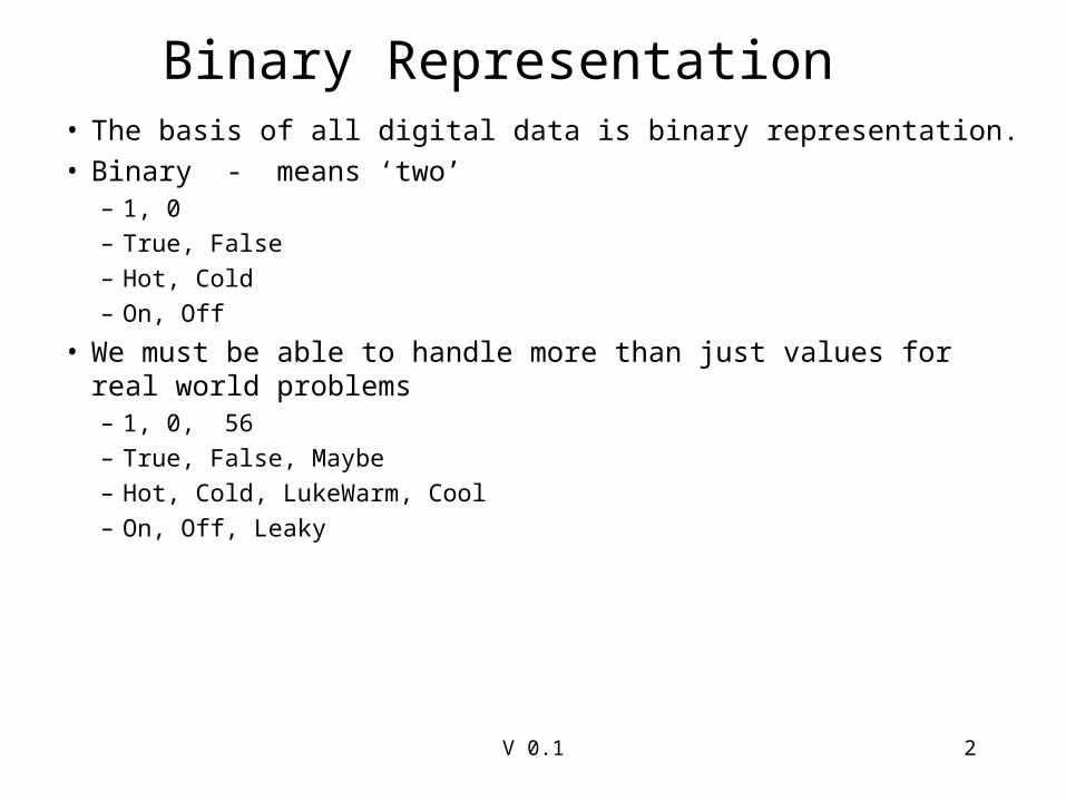
Binary Representation• The basis of all digital data is binary representation.• Binary - means ‘two’
– 1, 0– True, False– Hot, Cold– On, Off
• We must be able to handle more than just values for real world problems– 1, 0, 56– True, False, Maybe– Hot, Cold, LukeWarm, Cool– On, Off, Leaky
V 0.1 3
Number Systems
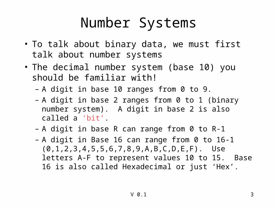
• To talk about binary data, we must first talk about number systems
• The decimal number system (base 10) you should be familiar with!– A digit in base 10 ranges from 0 to 9.– A digit in base 2 ranges from 0 to 1 (binary number system).
A digit in base 2 is also called a ‘bit’.– A digit in base R can range from 0 to R-1– A digit in Base 16 can range from 0 to 16-1
(0,1,2,3,4,5,5,6,7,8,9,A,B,C,D,E,F). Use letters A-F to represent values 10 to 15. Base 16 is also called Hexadecimal or just ‘Hex’.
V 0.1 4
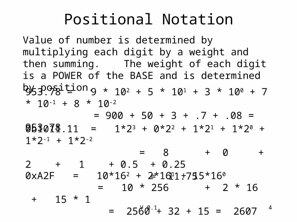
Positional NotationValue of number is determined by multiplying each digit by a weight and then summing. The weight of each digit is a POWER of the BASE and is determined by position.
953.78 = 9 * 102 + 5 * 101 + 3 * 100 + 7 * 10-1 + 8 * 10-2
= 900 + 50 + 3 + .7 + .08 = 953.78
0b1011.11 = 1*23 + 0*22 + 1*21 + 1*20 + 1*2-1 + 1*2-2
= 8 + 0 + 2 + 1 + 0.5 + 0.25 = 11.75
0xA2F = 10*162 + 2*161 + 15*160 = 10 * 256 + 2 * 16 + 15 * 1 = 2560 + 32 + 15 = 2607

V 0.1 5
Base 10, Base 2, Base 16The textbook uses subscripts to represent different bases (ie. A2F16 , 953.7810, 1011.112 )
I will use special symbols to represent the different bases.The default base will be decimal, no special symbol for base 10.
The ‘0x’ will be used for base 16 ( 0xA2F)The ‘0b’ will be used for base 2 (0b10101111)
If ALL numbers on a page are the same base (ie, all in base 16 or base 2 or whatever) then no symbols will be used and a statement will be present that will state the base (ie, all numbers on this page are in base 16).

V 0.1 6
Common Powers
2-3 = 0.1252-2 = 0.252-1 = 0.520 = 121 = 222 = 423 = 824 = 1625 =3226 = 6427 = 12828 = 25629 = 512210 = 1024211 = 2048212 = 4096
160 = 1 = 20
161 = 16 = 24
162 = 256 = 28
163 = 4096 = 212
210 = 1024 = 1 K220 = 1048576 = 1 M (1 Megabits) = 1024 K = 210 * 210
230 = 1073741824 = 1 G (1 Gigabits)

V 0.1 7
Conversion of Any Base to Decimal
Converting from ANY base to decimal is done by multiplying each digit by its weight and summing.
0b1011.11 = 1*23 + 0*22 + 1*21 + 1*20 + 1*2-1 + 1*2-2
= 8 + 0 + 2 + 1 + 0.5 + 0.25 = 11.75
Binary to Decimal
Hex to Decimal
0xA2F = 10*162 + 2*161 + 15*160 = 10 * 256 + 2 * 16 + 15 * 1 = 2560 + 32 + 15 = 2607

V 0.1 8
Conversion of Decimal Integer To ANY Base
Divide Number N by base R until quotient is 0. Remainder at EACH step is a digit in base R, from Least Significant digit to Most significant digit.
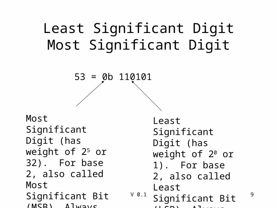
Convert 53 to binary 53/2 = 26, rem = 1 26/2 = 13, rem = 0 13/2 = 6 , rem = 1 6 /2 = 3, rem = 0 3/2 = 1, rem = 1 1/2 = 0, rem = 1
53 = 0b 110101 = 1*25 + 1*24 + 0*23 + 1*22 + 0*21 + 1*20
= 32 + 16 + 0 + 4 + 0 + 1 = 53
Least Significant Digit
Most Significant Digit
V 0.1 9
Least Significant DigitMost Significant Digit
53 = 0b 110101
Most Significant Digit (has weight of 25 or 32). For base 2, also called Most Significant Bit (MSB). Always LEFTMOST digit.
Least Significant Digit (has weight of 20 or 1). For base 2, also called Least Significant Bit (LSB). Always RIGHTMOST digit.

V 0.1 10
More Conversions
Convert 53 to Hex
53/16 = 3, rem = 5 3 /16 = 0 , rem = 3 53 = 0x35 = 3 * 161 + 5 * 160
= 48 + 5 = 53

V 0.1 11
Hex (base 16) to Binary Conversion
Each Hex digit represents 4 bits. To convert a Hex number to Binary, simply convert each Hex digit to its four bit value.
Hex Digits to binary:0x0 = 0b 00000x1 = 0b 00010x2 = 0b 00100x3 = 0b 00110x4 = 0b 01000x5 = 0b 01010x6 = 0b 01100x7 = 0b 01110x8 = 0b 1000
Hex Digits to binary (cont):0x9 = 0b 10010xA = 0b 10100xB = 0b 10110xC = 0b 11000xD = 0b 11010xE = 0b 11100xF = 0b 1111

V 0.1 12
Hex to Binary, Binary to Hex
0xA2F = 0b 1010 0010 1111
0x345 = 0b 0011 0100 0101
Binary to Hex is just the opposite, create groups of 4 bits starting with least significant bits. If last group does not have 4 bits, then pad with zeros for unsigned numbers.
0b 1010001 = 0b 0101 0001 = 0x51
Padded with a zero

V 0.1 13
A Trick!If faced with a large binary number that has to be converted to decimal, I first convert the binary number to HEX, then convert the HEX to decimal. Less work!
0b 110111110011 = 0b 1101 1111 0011 = D F 3 = 13 * 162 + 15 * 161 + 3*160
= 13 * 256 + 15 * 16 + 3 * 1 = 3328 + 240 + 3 = 3571
Of course, you can also use the binary, hex conversion feature on your calculator. Too bad calculators won’t be allowed on the first test, though…...
V 0.1 14
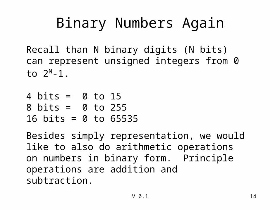
Binary Numbers Again
Recall than N binary digits (N bits) can represent unsigned integers from 0 to 2N-1.
4 bits = 0 to 158 bits = 0 to 25516 bits = 0 to 65535
Besides simply representation, we would like to also do arithmetic operations on numbers in binary form. Principle operations are addition and subtraction.

V 0.1 15
Binary Arithmetic, Subtraction
The rules for binary arithmetic are:
0 + 0 = 0, carry = 0
1 + 0 = 1, carry = 0
0 + 1 = 1, carry = 0
1 + 1 = 0, carry = 1
The rules for binary subtraction are:
0 - 0 = 0, borrow = 0
1 - 0 = 1, borrow = 0
0 - 1 = 1, borrow = 1
1 - 1 = 0, borrow = 0
Borrows, Carries from digits to left of current of digit.
Binary subtraction, addition works just the same as decimal addition, subtraction.

V 0.1 16
Binary, Decimal addition
34
+ 17------ 51from LSD to MSD:7+4 = 1; with carry out of 1 to next column
1 (carry) + 3 + 1 = 5.answer = 51.
Decimal 0b 101011
+ 0b 000001--------------- 101100From LSB to MSB:1+1 = 0, carry of 11 (carry)+1+0 = 0, carry of 11 (carry)+0 + 0 = 1, no carry1 +0 = 10 + 0 = 0 1 + 0 = 1 answer = % 101100
Binary
V 0.1 17
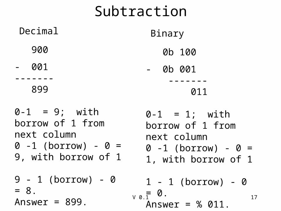
SubtractionDecimal
900
- 001------- 899
0-1 = 9; with borrow of 1 from next column0 -1 (borrow) - 0 = 9, with borrow of 1 9 - 1 (borrow) - 0 = 8.Answer = 899.
Binary
0b 100
- 0b 001 ------- 011
0-1 = 1; with borrow of 1 from next column0 -1 (borrow) - 0 = 1, with borrow of 1 1 - 1 (borrow) - 0 = 0.Answer = % 011.

V 0.1 18
Hex Addition
0x3A
+ 0x28-------- 0x62
A+8 = 2; with carry out of 1 to next column
1 (carry) + 3 + 2 = 6.answer = 0x62
0x3A = 3 * 16 + 10 = 58 0x28 = 2 * 16 + 8
= 40 58 + 40 = 98
0x62 = 6 * 16 + 2 = 96 + 2 = 98!!
Decimal check.

V 0.1 19
Hex addition againWhy is 0xA + 0x8 = 2 with a carry out of 1?
The carry out has a weight equal to the BASE (in this case 16). The digit that gets left is the excess (BASE - sum).
Ah + 8h = 10 + 8 = 18.
18 is GREATER than 16 (BASE), so need a carry out!
Excess is 18 - BASE = 18 - 16 = 2, so ‘2’ is digit.
Exactly the same thing happens in Decimal. 5 + 7 = 2, carry of 1. 5 + 7 = 12, this is greater than 10!.So excess is 12 - 10 = 2, carry of 1.
V 0.1 20
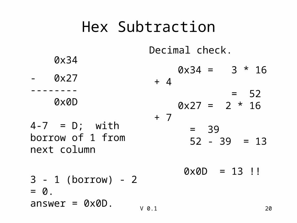
Hex Subtraction
0x34
- 0x27-------- 0x0D
4-7 = D; with borrow of 1 from next column
3 - 1 (borrow) - 2 = 0.answer = 0x0D.
0x34 = 3 * 16 + 4 = 52 0x27 = 2 * 16 + 7
= 39 52 - 39 = 13
0x0D = 13 !!
Decimal check.
V 0.1 21
Hex subtraction again
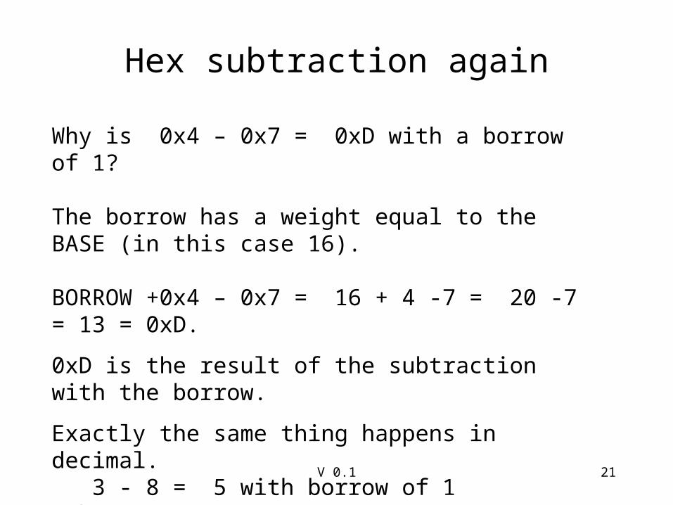
Why is 0x4 – 0x7 = 0xD with a borrow of 1?
The borrow has a weight equal to the BASE (in this case 16).
BORROW +0x4 – 0x7 = 16 + 4 -7 = 20 -7 = 13 = 0xD.
0xD is the result of the subtraction with the borrow.
Exactly the same thing happens in decimal. 3 - 8 = 5 with borrow of 1 borrow + 3 - 8 = 10 + 3 - 8 = 13 - 8 = 5.

V 0.1 22
Fixed PrecisionWith paper and pencil, I can write a number with as many digits as I want:
1,027,80,032,034,532,002,391,030,300,209,399,302,992,092,920
A microprocessor or computing system usually uses FIXED PRECISION for integers; they limit the numbers to a fixed number of bits:
0x AF4500239DEFA231 64 bit number, 16 hex digits0x 9DEFA231 32 bit number, 8 hex digits0x A231 16 bit number, 4 hex digits0x 31 8 bit number, 2 hex digits
High end microprocessors use 64 or 32 bit precision; low end microprocessors use 16 or 8 bit precision.
V 0.1 23
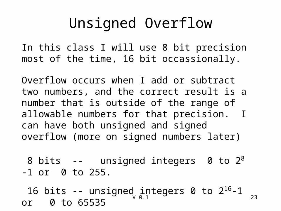
Unsigned Overflow
In this class I will use 8 bit precision most of the time, 16 bit occassionally.
Overflow occurs when I add or subtract two numbers, and the correct result is a number that is outside of the range of allowable numbers for that precision. I can have both unsigned and signed overflow (more on signed numbers later)
8 bits -- unsigned integers 0 to 28 -1 or 0 to 255.
16 bits -- unsigned integers 0 to 216-1 or 0 to 65535

V 0.1 24
Unsigned Overflow ExampleAssume 8 bit precision; ie. I can’t store any more than 8 bits for each number.
Lets add 255 + 1 = 256. The number 256 is OUTSIDE the range of 0 to 255! What happens during the addition?
255 = 0x FF
+ 1 = 0x 01------------------- 256 /= 0x00
0xF + 1 = 0, carry out0xF + 1 (carry) + 0 = 0, carry outCarry out of MSB falls off end, No place to put it!!!Final answer is WRONG because could not store carry out.
/= means Not Equal
V 0.1 25
Unsigned Overflow
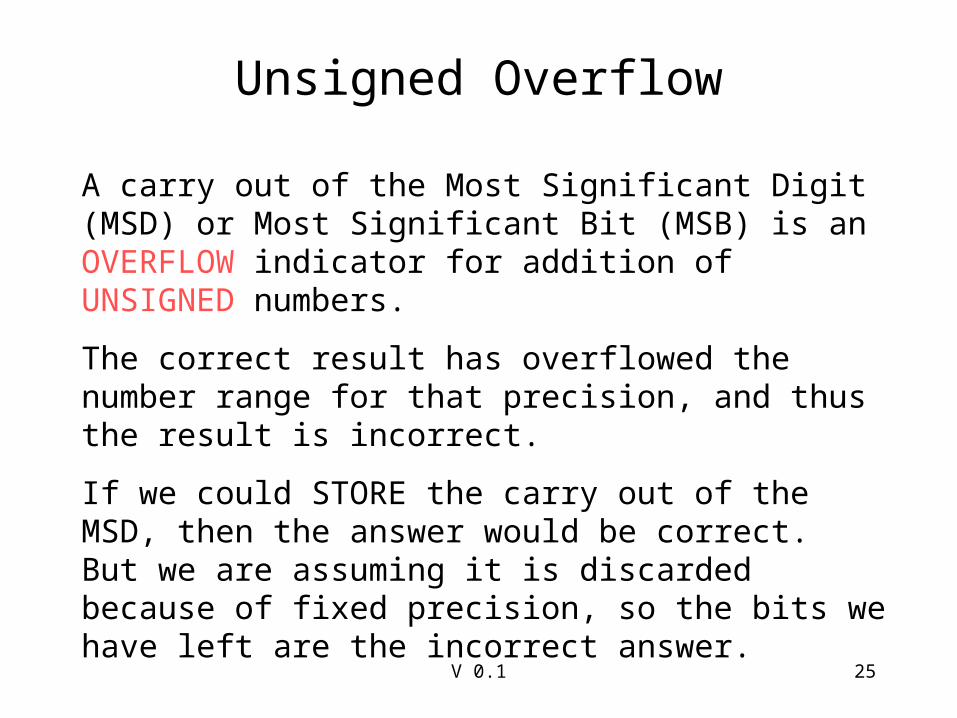
A carry out of the Most Significant Digit (MSD) or Most Significant Bit (MSB) is an OVERFLOW indicator for addition of UNSIGNED numbers.
The correct result has overflowed the number range for that precision, and thus the result is incorrect.
If we could STORE the carry out of the MSD, then the answer would be correct. But we are assuming it is discarded because of fixed precision, so the bits we have left are the incorrect answer.

V 0.1 26
Binary Codes (cont.)
N bits (or N binary Digits) can represent 2N different values.
(for example, 4 bits can represent 24 or 16 different values)
N bits can take on unsigned decimal values from 0 to 2N-1.
Codes usually given in tabular form.
000001010011100101110111
blackredpinkyellowbrownbluegreenwhite
V 0.1 27
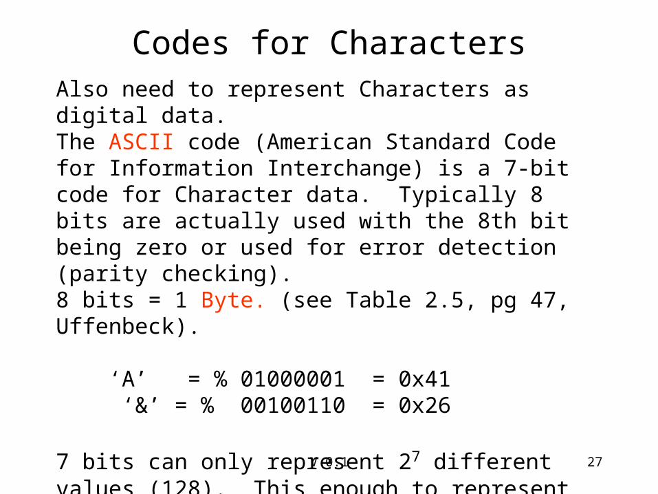
Codes for CharactersAlso need to represent Characters as digital data. The ASCII code (American Standard Code for Information Interchange) is a 7-bit code for Character data. Typically 8 bits are actually used with the 8th bit being zero or used for error detection (parity checking).8 bits = 1 Byte. (see Table 2.5, pg 47, Uffenbeck).
‘A’ = % 01000001 = 0x41 ‘&’ = % 00100110 = 0x26
7 bits can only represent 27 different values (128). This enough to represent the Latin alphabet (A-Z, a-z, 0-9, punctuation marks, some symbols like $), but what about other symbols or other languages?

V 0.1 28
ASCIIAmerican Standard Code for Information Interchange

V 0.1 29
UNICODEUNICODE is a 16-bit code for representing alphanumeric data. With 16 bits, can represent 216 or 65536 different symbols.16 bits = 2 Bytes per character (the extended version uses 32-bits per character, or 4 bytes, for 4,294,967,296 different symbols).
0x0041-005A A-Z0x0061-4007A a-z
Some other alphabet/symbol ranges
0x3400-3d2d Korean Hangul Symbols0x3040-318F Hiranga, Katakana, Bopomofo, Hangul0x4E00-9FFF Han (Chinese, Japenese, Korean)
UNICODE used by Web browsers, Java, most software these days.

V 0.1 30
7404 Logic Gate
A YL HH L
A (A) (L)
Buffer that converts high true input to low true output
Buffer that converts low true input to high true output
A Y (L)0 01 1
A(L) AA(L) Y1 10 0A Y
0 11 0
Mixed Logic
Fixed Logic
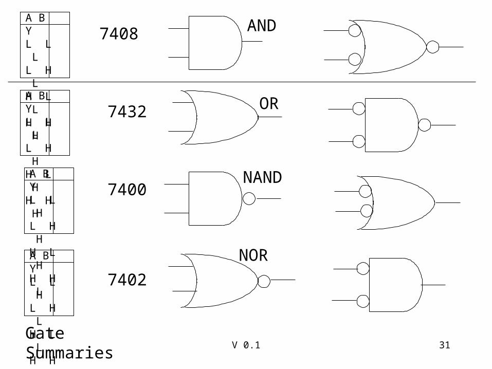
V 0.1 31
7408
7432
7400
7402
Gate Summaries
A B YL L HL H HH L HH H L
A B YL L LL H HH L HH H H
A B YL L LL H LH L LH H H
A B YL L HL H LH L LH H L
AND
OR
NAND
NOR

V 0.1 32
Majority Gate (and-or) form
A
B
C
AC
AB
BC
F = AB + AC + BC
A B C F 0 0 0 0 0 0 1 0 0 1 0 0 0 1 1 1 1 0 0 0 1 0 1 1 1 1 0 1 1 1 1 1

V 0.1 33
Majority Gate (mixed logic) formA
B
C
(AC) L
(AB) L
(BC) L
A B C F 0 0 0 0 0 0 1 0 0 1 0 0 0 1 1 1 1 0 0 0 1 0 1 1 1 1 0 1 1 1 1 1
F = AB + AC + BC

V 0.1 34
Representing ‘1’ and ‘0’
• In the electrical world, two ways of representing ‘0’ and ‘1’ are (these are not the only ways):– Presence or absence of electrical current
– Different Voltage levels
• Different voltage levels are the most common– Usually 0v for logic ‘0’, some non-zero voltage for logic ‘1’ (I.e.
> 3 volts)
• Can interface external sources to digital systems in many ways– Switches, buttons, other human controlled input devices
– Transducers (change a physical quantity like temperature into a digital quantity).

V 0.1 35
Switch Inputs
Vdd
Gnd
L
Vdd
Gnd
H
High True switch
Switch open (negated), output is L
Switch closed (asserted), output is H
Vdd is power supply voltage, typically 5V or 3.3V
Gnd is 0 V
V 0.1 36
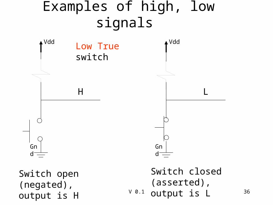
Examples of high, low signals
Vdd
Gnd
H
Vdd
Gnd
L
Low True switch
Switch open (negated), output is H
Switch closed (asserted), output is L

V 0.1 37
CMOS Transistors (N-type)
g
s
d
N-type (NMOS) transistor - can think of it as a switch.
g: gate, d: drain, s: source
g = H
d s
When g= H, d is connected to s (current flows between s, d because switch is closed.
s
g
d
d s
g = L
d s d s
When g= L, d is disconnected from s (current does not flow between s, d because switch is open.
V 0.1 38
CMOS Transistors (P-type)
g
s
d
P-type (PMOS) transistor - can think of it as a switch.
g: gate, d: drain, s: source
g = L
d s
When g= L, d is connected to s (current flows between s, d because switch is closed.
s
g
d
d s
g = H
d s d s
When g= H, d is disconnected from s (current does not flow between s, d because switch is open.

V 0.1 39
Inverter gate - takes 2 Transistors
A Y+5v
A Y
PMOS
NMOS

V 0.1 40
Inverter Operation
PMOS is open (off)
A=H Y = L
NMOS is Closed (on)
PMOS is closed (on)
A=L Y = H
NMOS is Open (cff)
A YL HH LA Y

V 0.1 41
NAND gate - takes 4 Transistors
+5v
A
PMOS
NMOS
B
B
Y
NMOS
PMOSA B YL L HL H HH L HH H L
A
B
Y

V 0.1 42
NAND Gate operation
A=L B=L
A=L
B=L nmos open
nmos open
Y=H
A B YL L HL H HH L HH H L
pmos closed
pmos closed
A=L B=H
A=L
B=H nmos closed
nmos open
Y=H
pmos open
pmos closed
A
BY

V 0.1 43
NAND Gate operation (continued)
A=H B=L
A=H
B=L nmos open
nmos closed
Y=H
A B YL L HL H HH L HH H L
pmos closed
pmos open
A=H B=H
A=H
B=H nmos closed
nmos closed
Y=L
pmos open
pmos open
A
BY

V 0.1 44
How do we make an AND gate?
The only way with CMOS transistors is to connect an inverter after a NAND gate.
Y = AB A
B
A
B
Y = AB
A B YL L LL H LH L LH H H
Takes 6 transistors! In CMOS technology, NAND gates are preferable to AND gates because they take less transistors, are faster, and consume less power.
4 transistors 2 transistors
6 transistors

V 0.1 45
Tri State BufferThere is another way to drive a line or bus from multiple sources. Use a TRISTATE buffer.
A Y
EN
When EN = 1, then Y = A.
When EN = 0, then Y = ?????? Y is undriven, this is called the high impedance state.
Designate high impedance by a ‘Z’.
When EN = 0, then Y = ‘Z’ (high impedance)
A Y
EN
V 0.1 46
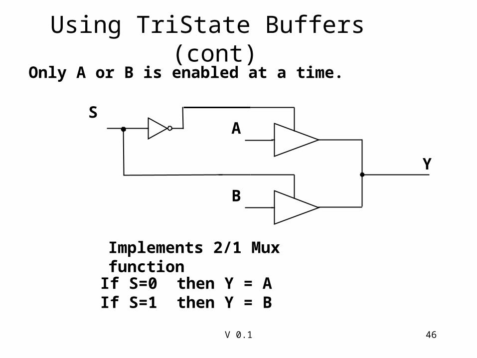
Using TriState Buffers (cont)Only A or B is enabled at a time.
A
Y
B
S
Implements 2/1 Mux function
If S=0 then Y = AIf S=1 then Y = B
V 0.1 47
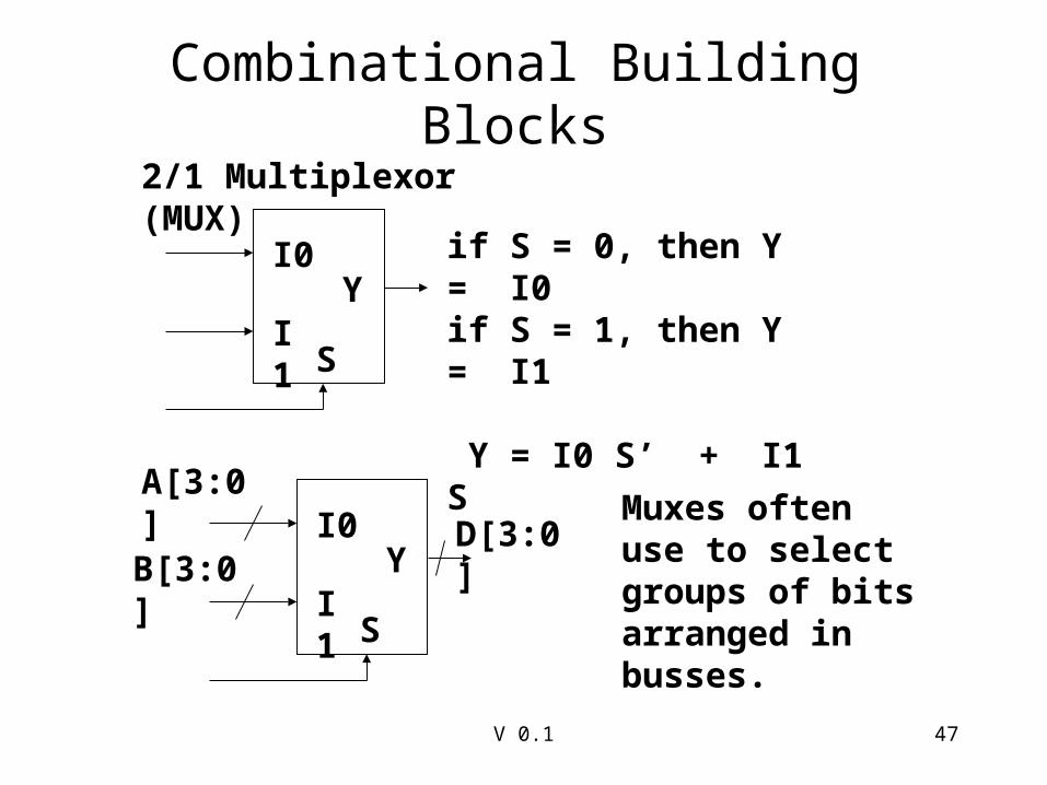
Combinational Building Blocks
2/1 Multiplexor (MUX)
I0
I1Y
S
if S = 0, then Y = I0if S = 1, then Y = I1
Y = I0 S’ + I1 S
I0
I1Y
S
A[3:0]
B[3:0]D[3:0]
Muxes often use to select groups of bits arranged in busses.

V 0.1 48
Logic for 2/1, 4/1 Muxes
I0
Y = I0 S’ + I1 S
S’ I1 S
Y
Y = I0 S1’ S0’ + I1 S1’ S0 + I2 S1 S0’ + I3 S1 S0
I0S0’S1’I1S0S1’
I2S0’S1I3S0S1
Y S[1:0]
2
These are called COMBINATIONAL muxes.

V 0.1 49
N-Bit Wide Elements
To build a 2/1 mux for 4-bit wide busses, need four 1-bit 2/1 muxes.
I0
I1Y
S
A[3:0]
B[3:0]D[3:0]
I0I1
Y
S
I0I1
Y
S
I0I1
Y
S
I0I1
Y
S
A0B0
A1B1
A2B2
A3B3
Y0
Y1
Y2
Y3
S
V 0.1 50
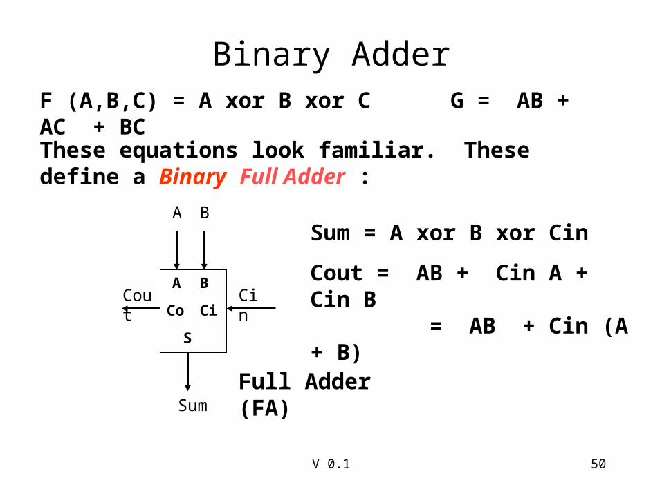
Binary AdderF (A,B,C) = A xor B xor C G = AB + AC + BC
These equations look familiar. These define a Binary Full Adder :
A B
S
CiCoCin
A B
Cout
Sum
Sum = A xor B xor Cin
Cout = AB + Cin A + Cin B = AB + Cin (A + B)
Full Adder (FA)
V 0.1 51
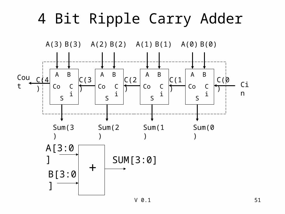
4 Bit Ripple Carry Adder
A B
S
CiCo
A B
S
CiCo
A B
S
CiCo
A B
S
CiCo Cin
A(0)
Cout
B(0)A(1) B(1)A(2) B(2)A(3) B(3)
C(0)C(1)C(2)C(3)C(4)
Sum(0)Sum(1)Sum(2)Sum(3)
A[3:0]
B[3:0]
SUM[3:0]+

V 0.1 52
Incrementer
A(0)A(1)A(2)A(3)
EN
Y(0)Y(1)Y(2)Y(3)
A[3:0]
EN
Y[3:0]incIf EN = 1 then Y = A + 1If EN = 0 then Y = A
xor xor xor xor

V 0.1 53
Recall Basic Memory Definition
MEM
Data[N-1:0]Address[log2(K)-1:0]
K x N
K locations, N bits per location
Address bus has log2(K) address lines, data bus has N data lines.
V 0.1 54
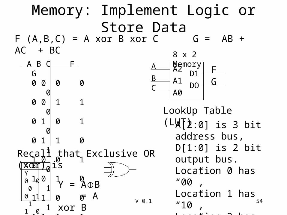
Memory: Implement Logic or Store DataF (A,B,C) = A xor B xor C G = AB + AC + BC
A B C F G 0 0 0 0 0 0 0 1 1 0 0 1 0 1 0 0 1 1 0 1 1 0 0 1 0 1 0 1 0 1 1 1 0 0 1 1 1 1 1 1 Recall that Exclusive OR (xor) is
A B Y0 0 00 1 11 0 11 1 0
Y = AB = A xor B
A0
A1
A2
8 x 2 Memory
A
BC DO G
LookUp Table (LUT)
D1 F
A[2:0] is 3 bit address bus, D[1:0] is 2 bit output bus.Location 0 has “00”, Location 1 has “10”,Location 2 has “10”, etc….

V 0.1 55
Sequential System Diagram
CombinationalLogicCircuit
Memory Elements - flip-flop - latch - register - PROM
n m
k k
k-bitPresent State
Value
k-bitNext State
Value
• m outputs only depend on k PS bits - Moore Machine– REMEMBER: Moore is Less !!
• m outputs depend on k PS bits AND n inputs - Mealy MachineSlide by Prof Mitch Thorton

V 0.1 56
Clock Signal Review
time
voltage
f = 1/
Pw rising edge falling edge
- period (in seconds) Pw - pulse width (in seconds)
f - frequency pulse width (in Hertz)
duty cycle - ratio of pulse width to period (in %) duty cycle = Pw /
millisecond (ms)10-3
Kilohertz (KHz)103
microsecond (s)10-6
Megahertz (MHz)106
nanosecond (ns)10-9
Gigahertz (GHz)109
Slide by Prof Mitch Thorton
V 0.1 57
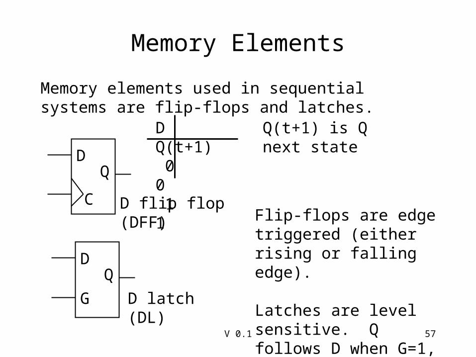
Memory Elements
Memory elements used in sequential systems are flip-flops and latches.
DQ
C
D Q(t+1) 0 0 1 1
Q(t+1) is Q next state
D flip flop (DFF)
DQ
G D latch (DL)
Flip-flops are edge triggered (either rising or falling edge).
Latches are level sensitive. Q follows D when G=1, latches when G goes from 1 to 0.

V 0.1 58
D FF, D Latch operation
C for FF, G for latch
D input
Q (FF)
Q (DL)

V 0.1 59
Synchronous vs Asynchronous Inputs
Synchronous input: Output will change after active clock edgeAsychronous input: Output changes independent of clock
DQ
C
S
R
State elements often have async set, reset control.
D input is synchronous with respect to Clk
S, R are asynchronous. Q output affected by S, R independent of C. Async inputs are dominant over Clk.
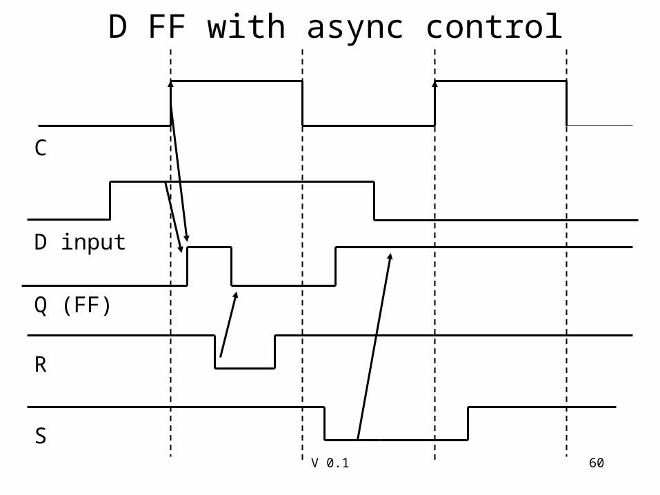
V 0.1 60
D FF with async control
C
D input
Q (FF)
R
S

V 0.1 61
RegistersThe most common sequential building block is the register. A register is N bits wide, and has a load line for loading in a new value into the register.
DIN
NCLK
LD
REG
DOUT
N
Register contents do not change unless LD = 1 on active edge of clock.
A DFF is NOT a register! DFF contents change every clock edge.
ACLR used to asynchronously clear the register
ACLR

V 0.1 62
1 Bit Register using DFF, Mux
DQ
C
0
1
S
Y
2/1 Mux DFF
DOUT DIN
LD
CLK
Note that DFF simply loads old value when LD = 0. DFF is loaded every clock cycle.
R
ACLR
V 0.1 63
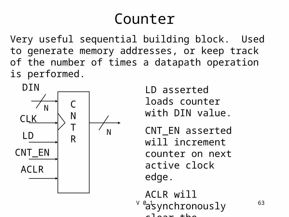
CounterVery useful sequential building block. Used to generate memory addresses, or keep track of the number of times a datapath operation is performed.
DIN
N
CLK
LD
CNTR
N
CNT_EN
ACLR
LD asserted loads counter with DIN value.
CNT_EN asserted will increment counter on next active clock edge.
ACLR will asynchronously clear the counter.
V 0.1 64
One way to build a Counter
DINN
NR
DFF0
1
S
Y
EN
CNT_EN
DIN
LDCLK
ACLR
N
N
DINY
Incrementer

V 0.1 65
Shift RegisterVery useful sequential building block. Used to perform either parallel to serial data conversion or serial to parallel data conversion.
DIN
N
CLK
LD
SHIFTER
EN
ACLR
LD asserted loads register with DIN value.
EN asserted will shift data on next active clock edge.
ACLR is async clear.
SI is serial data in.
Look at LSB of DOUT for serial data out.
SI
N
DOUT

V 0.1 66
Understanding the shift operation
0x85 = 1 0 0 0 0 1 0 1
0x42 = 0 1 0 0 0 0 1 0
SI = 0
MSB LSB
0x21 = 0 0 1 0 0 0 0 1
SI = 0
1st right shift
2nd right shift
0x10 = 0 0 0 1 0 0 0 0
SI = 0
3rd right shift
Etc….

V 0.1 67
Right Shift vs Left ShiftA right shift is MSB to LSB
In: D7 D6 D5 D4 D3 D2 D1 D0
SIN
Out: SIN D7 D6 D5 D4 D3 D2 D1
A left shift is LSB to MSB
In: D7 D6 D5 D4 D3 D2 D1 D0
SI
Out: D6 D5 D4 D3 D2 D1 D0 SI

V 0.1 68
Combinational Right Shifter
We need a combinational block that can either shift right or pass data unchanged
EN
D Y
SRIGHT
NN
When EN = 1, Y = D shifted right by 1 position.
When EN=0, Y = DSI

V 0.1 69
I0I1
Y
S
I0I1
Y
S
I0I1
Y
S
I0I1
Y
S
D0D1
D1D2
D2D3
D3SI
Y0
Y1
Y2
Y3
EN
4-bit Combinational RIGHT Shifter Implementation
When EN = 0, then:
Y = D3 D2 D1 D0
When EN = 1, then:
Y = SI D3 D2 D1
(right shifted by one position)

V 0.1 70
Shift Register (Right shift) Implementation
DN
NR
DFF0
1
S
Y
SI
SI
DIN
LDCLK
ACLR
N
N
DY
Right Shifter
Q
ENEN

V 0.1 71
What do you need to Know?• Convert hex, binary integers to Decimal• Convert decimal integers to hex, binary• Convert hex to binary, binary to Hex• N binary digits can represent 2N values, unsigned
integers 0 to 2N-1.• Addition, subtraction of binary, hex numbers• Detecting unsigned overflow

V 0.1 72
What do you need to know? (cont)
• ASCII, UNICODE are binary codes for character data
• Basic two-input Logic Gate operation• NMOS/PMOS Transistor Operations• Inverter/NAND transistor configurations• Tri-state buffer operation• Mux, Memory, Adder operation• Clock signal definition• DFF, Register, Counter, Shifter register operation