uw-madison computer sciences vertical research group© 2010 a unified model for timing speculation:...
TRANSCRIPT

UW-Madison Computer Sciences Vertical Research Group © 2010
A Unified Model for Timing Speculation: Evaluating the Impact of Technology Scaling, CMOS
Design Style, and Fault Recovery Mechanism
Marc de KruijfShuou Nomura
Karu Sankaralingam
DSN 2010 - 2
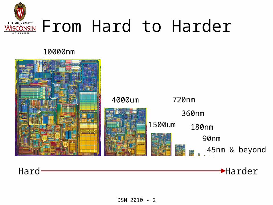
From Hard to Harder
45nm & beyond90nm
180nm
360nm
720nm
1500um
4000um
10000nm
Hard Harder

DSN 2010 - 3
What is the Problem?
Non-ideal transistor scaling Transistor wear-out Process, voltage, and temperature (PVT) variations Errors due to particle interference Noise coupling & crosstalk

DSN 2010 - 4
What is the Problem?
DMR
Timing s
peculati
on
RMT
HW checkpoints
TMRECC
Watchdog
DynamicverificationMulti-core
Coherence &
consistency
On-chip netw
ork
Out-of-order
Branchprediction
Performance Toolbox Reliability Toolbox
NEED HIGH-LEVEL ANALYSIS TOOLS

DSN 2010 - 5
Our Contribution
Also….
Q. What is the impact of technology scaling? A. Further benefits are small to none.
Q. What is the impact of CMOS design style? A. Very low power designs benefit most.
Q. What is the impact of the fault recovery mechanism?A. Fine-grained recovery is key to high efficiencies.
A model for timing speculation• Unifies hardware + system• Small set of high-level inputs
processordesigner
DSN 2010 - 6
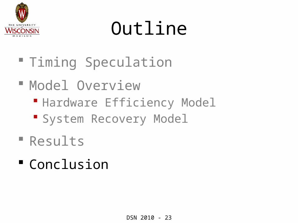
Outline
Timing Speculation
Model Overview Hardware Efficiency Model System Recovery Model
Results
Conclusion

DSN 2010 - 7
Timing Speculation
…clock
circuit delay
clock period ( = 1/frequency )
Timing failure!variations
OK!
slower clock
detect &recover
…

DSN 2010 - 8
Outline
Timing Speculation
Model Overview Hardware Efficiency Model System Recovery Model
Results
Conclusion
DSN 2010 - 9
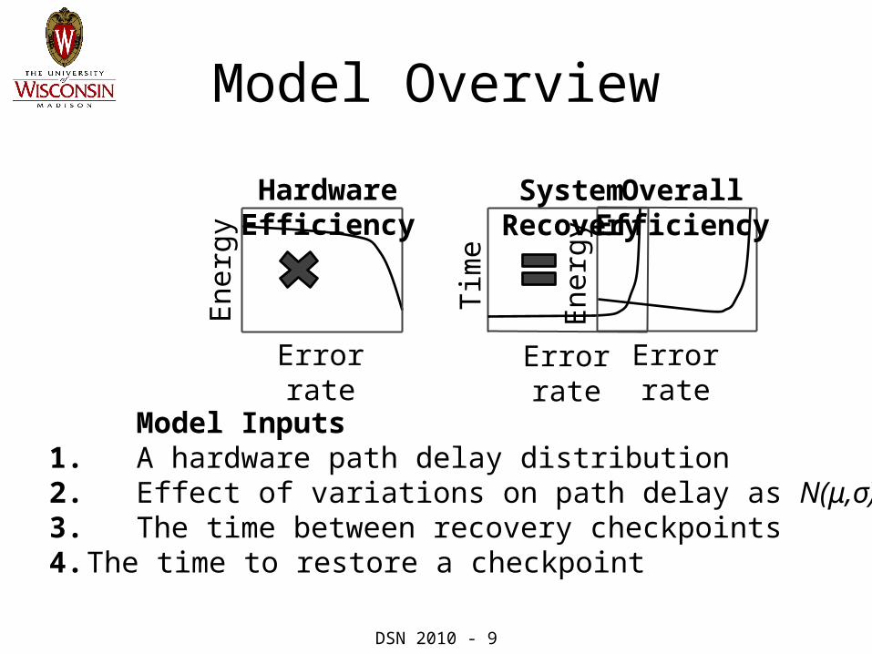
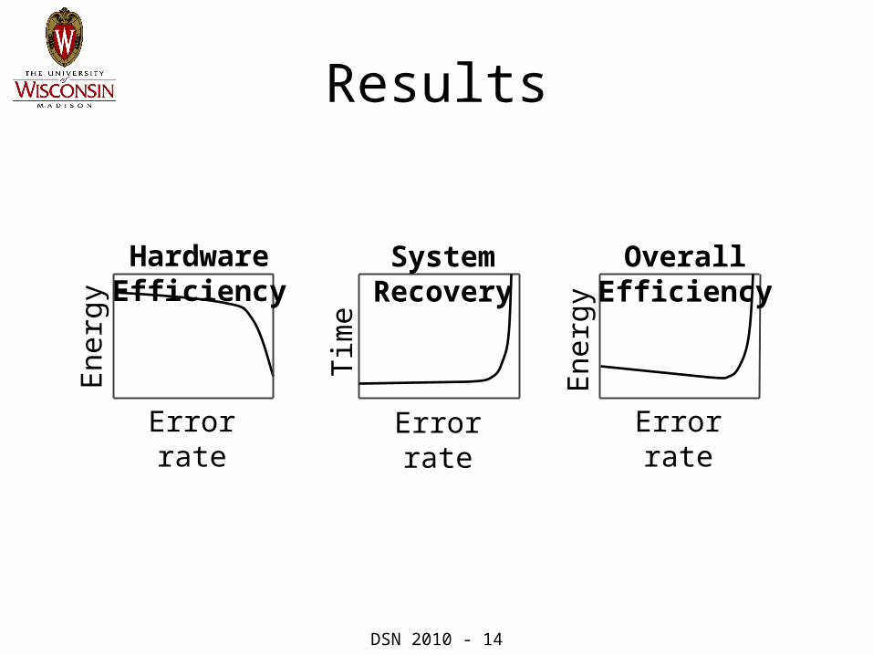
Model Overview
Error rate Error rateError rate
Tim
e
Hardware Efficiency System RecoveryOverall EfficiencyEn
ergy
Ener
gy
Model Inputs1. A hardware path delay distribution2. Effect of variations on path delay as N(μ,σ)3. The time between recovery checkpoints4. The time to restore a checkpoint
DSN 2010 - 10
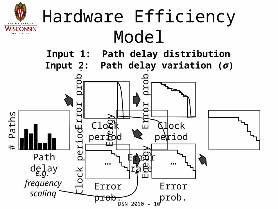
Hardware Efficiency Model#
Path
s
Path delay
Err
or p
rob.
Clock period
Error rate
Ener
gy
Input 1: Path delay distributionInput 2: Path delay variation (σ)
Err
or p
rob.
Clock period
Cloc
k pe
riod
Error prob.
Ener
gy
Error prob.
… …e.g.
frequencyscaling
DSN 2010 - 11
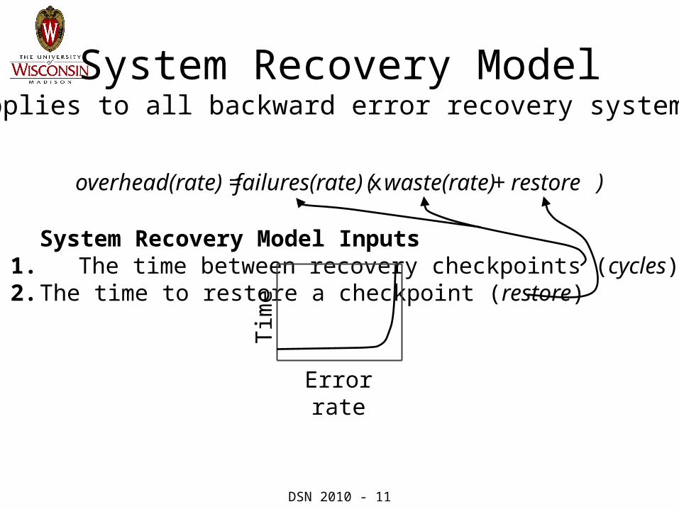
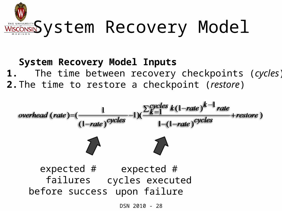
System Recovery Model
System Recovery Model Inputs1. The time between recovery checkpoints (cycles)2. The time to restore a checkpoint (restore)
overhead(rate) = failures(rate) x waste(rate) + restore( )
Error rate
Tim
e
(applies to all backward error recovery systems)

DSN 2010 - 12
Outline
Timing Speculation
Model Overview Hardware Efficiency Model System Recovery Model
Results
Conclusion

DSN 2010 - 13
Results
High Performance CMOSLow Power CMOS
Ultra-low Power CMOS
RazorReunionPaceline
11nm45nm
Is the model useful?What can we learn?
CMOS Design StyleTechnology
NodeRecoverySystem
DSN 2010 - 14
Results
Error rate Error rate Error rate
Tim
e
Hardware Efficiency System Recovery Overall Efficiency
Ener
gy
Ener
gy

DSN 2010 - 15
Hardware Model Inputs
1. Path delay distribution Application: H.264 decoding Hardware: OpenRISC processor
2. Effect of process variations as N(μ,σ) using ITRS data High Performance CMOS
45nm σ = 0.046μ 11nm σ = 0.051μ
Low Power CMOS 45nm σ = 0.029μ 11nm σ = 0.042μ
Ultra-low Power CMOS 45nm σ = 0.196μ

DSN 2010 - 16
Hardware Efficiency
Error rate
Ener
gy
Results forHigh Performance CMOS
EDP Energy = Power x Time
EDP = Power x Time2
Nor
mal
ized
EDP
Error rate
DSN 2010 - 17
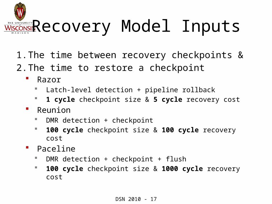
Recovery Model Inputs
1. The time between recovery checkpoints &2. The time to restore a checkpoint
Razor Latch-level detection + pipeline rollback 1 cycle checkpoint size & 5 cycle recovery cost
Reunion DMR detection + checkpoint 100 cycle checkpoint size & 100 cycle recovery cost
Paceline DMR detection + checkpoint + flush 100 cycle checkpoint size & 1000 cycle recovery cost

DSN 2010 - 18
System Recovery
Error rate
Tim
e
Nor
mal
ized
Tim
e
Error rate

DSN 2010 - 19
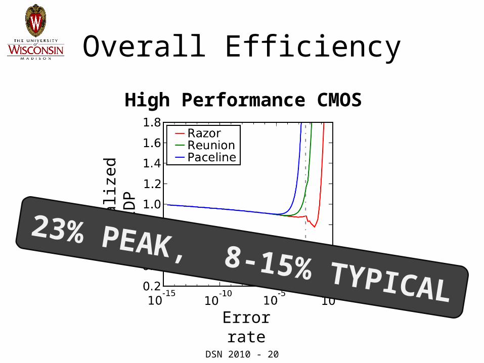
Overall Efficiency
Error rateED
P
1. High Performance CMOS
2. Low Power CMOS
3. Ultra-low Power CMOS
DSN 2010 - 20
Nor
mal
ized
EDP
Overall Efficiency
High Performance CMOS
23% PEAK, 8-15% TYPICALError rate

DSN 2010 - 21
Overall Efficiency
Low Power CMOS
18% PEAK, 5-10% TYPICAL
Error rate
Nor
mal
ized
EDP

DSN 2010 - 22
Nor
mal
ized
EDP
Overall Efficiency
Ultra-low Power CMOS
47% PEAK, 20-30% TYPICALError rate
DSN 2010 - 23
Outline
Timing Speculation
Model Overview Hardware Efficiency Model System Recovery Model
Results
Conclusion
DSN 2010 - 24
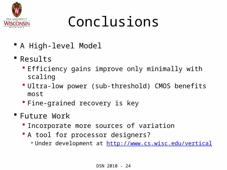
Conclusions
A High-level Model
Results Efficiency gains improve only minimally with scaling Ultra-low power (sub-threshold) CMOS benefits most Fine-grained recovery is key
Future Work Incorporate more sources of variation A tool for processor designers?
Under development at http://www.cs.wisc.edu/vertical

DSN 2010 - 25
Timing s
peculati
onMulti-core
Coherence &
consistency
On-chip netw
ork
Out-of-order
Branchprediction
Questions?

DSN 2010 - ‹#›
?
DSN 2010 - 27
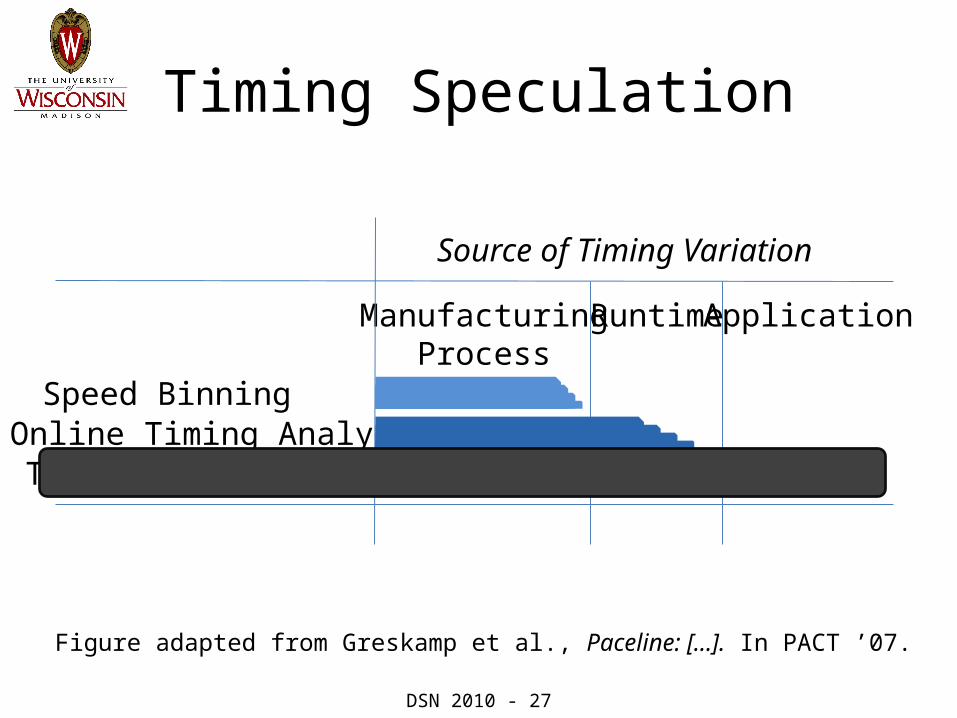
Timing Speculation
ManufacturingProcess
Runtime Application
Source of Timing Variation
Speed BinningOnline Timing AnalysisTiming Speculation
Figure adapted from Greskamp et al., Paceline: [...]. In PACT ’07.
DSN 2010 - 28
expected # cycles executed upon failure
System Recovery Model
System Recovery Model Inputs1. The time between recovery checkpoints (cycles)2. The time to restore a checkpoint (restore)
expected # failures before success
DSN 2010 - 29
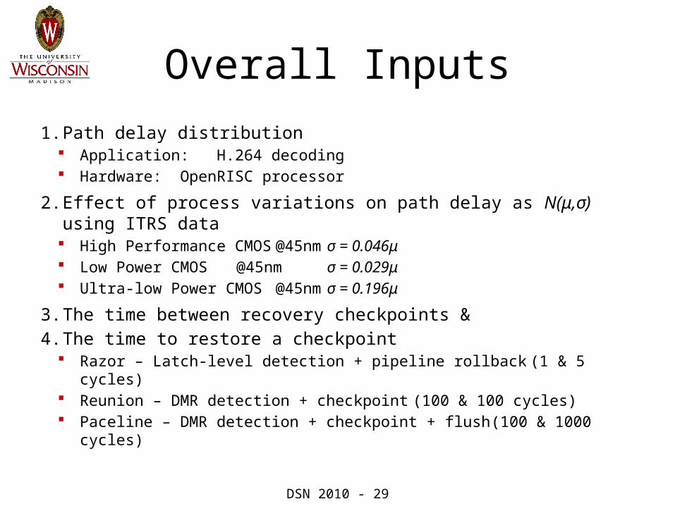
Overall Inputs
1. Path delay distribution Application: H.264 decoding Hardware: OpenRISC processor
2. Effect of process variations on path delay as N(μ,σ) using ITRS data High Performance CMOS @45nm σ = 0.046μ Low Power CMOS @45nm σ = 0.029μ Ultra-low Power CMOS @45nm σ = 0.196μ
3. The time between recovery checkpoints &4. The time to restore a checkpoint
Razor – Latch-level detection + pipeline rollback (1 & 5 cycles) Reunion – DMR detection + checkpoint (100 & 100 cycles) Paceline – DMR detection + checkpoint + flush (100 & 1000 cycles)