using library modules in verilog designsathena.ecs.csus.edu/~cpe64/s2015/handouts/labs/lab... ·...
TRANSCRIPT
Using Library Modulesin Verilog Designs
For Quartus II 13.0
1 Introduction
This tutorial explains how Altera’s library modules can be included in Verilog-based designs, which are implementedby using the Quartus® II software.
Contents:
• Example Circuit
• Library of Parameterized Modules
• Augmented Circuit with an LPM
• Results for the Augmented Design
Altera Corporation - University ProgramMay 2013
1

USING LIBRARY MODULES IN VERILOG DESIGNS For Quartus II 13.0
2 Background
Practical designs often include commonly used circuit blocks such as adders, subtractors, multipliers, decoders,counters, and shifters. Altera provides efficient implementations of such blocks in the form of library modules thatcan be instantiated in Verilog designs. The compiler may recognize that a standard function specified in Verilog codecan be realized using a library module, in which case it may automatically infer this module. However, many librarymodules provide functionality that is too complex to be recognized automatically by the compiler. These moduleshave to be instantiated in the design explicitly by the user. Quartus® II software includes a library of parameterizedmodules (LPM). The modules are general in structure and they are tailored to a specific application by specifyingthe values of general parameters.
Doing this tutorial, the reader will learn about:
• Library of parameterized modules (LPMs)
• Configuring an LPM for use in a circuit
• Instantiating an LPM in a designed circuit
The detailed examples in the tutorial were obtained using the Quartus II version 13.0, but other versions of thesoftware can also be used. When selecting a device within Quartus II, use the device names associated with FPGAchip on the DE-series board by referring to Table 1.
Board Device NameDE0 Cyclone III EP3C16F484C6
DE0-Nano Cyclone IVE EP4CE22F17C6DE1 Cyclone II EP2C20F484C7DE2 Cyclone II EP2C35F672C6
DE2-70 Cyclone II EP2C70F896C6DE2-115 Cyclone IVE EP4CE115F29C7
Table 1. DE-series FPGA device names
3 Example Circuit
As an example, we will use the adder/subtractor circuit shown in Figure 1. It can add, subtract, and accumulate n-bitnumbers using the 2’s complement number representation. The two primary inputs are numbers A = an−1an−2 · · ·a0
and B = bn−1bn−2 · · ·b0, and the primary output is Z = zn−1zn−2 · · ·z0. Another input is the AddSub control signalwhich causes Z = A+B to be performed when AddSub = 0 and Z = A−B when AddSub = 1. A second control input,Sel, is used to select the accumulator mode of operation. If Sel = 0, the operation Z = A±B is performed, but if Sel= 1, then B is added to or subtracted from the current value of Z . If the addition or subtraction operations result inarithmetic overflow, an output signal, Overflow, is asserted.
To make it easier to deal with asynchronous input signals, they are loaded into flip-flops on a positive edge of the
2 Altera Corporation - University ProgramMay 2013

USING LIBRARY MODULES IN VERILOG DESIGNS For Quartus II 13.0
clock. Thus, inputs A and B will be loaded into registers Areg and Breg, while Sel and AddSub will be loaded intoflip-flops SelR and AddSubR, respectively. The adder/subtractor circuit places the result into register Zreg.
Figure 1. The adder/subtractor circuit.
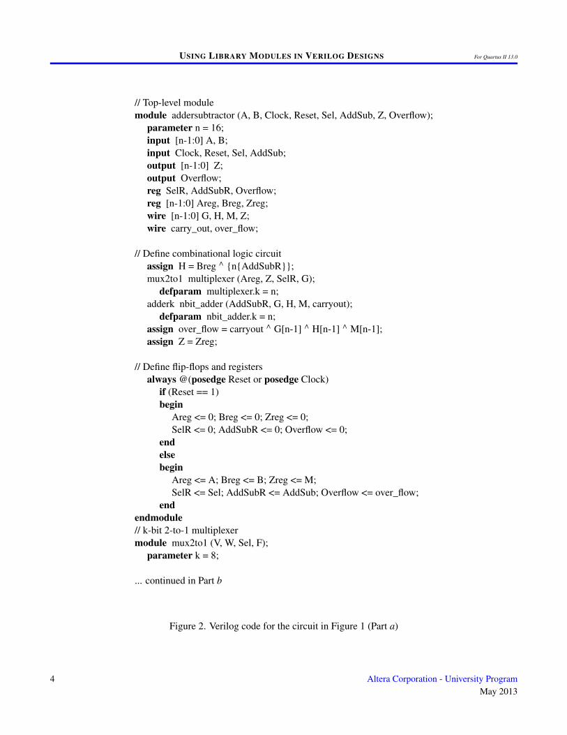
The required circuit is described by the Verilog code in Figure 2. For our example, we use a 16-bit circuit as specifiedby n = 16. Implement this circuit as follows:
• Create a project addersubtractor.
• Include a file addersubtractor.v, which corresponds to Figure 2, in the project. For convenience, this file isprovided in the design_files subdirectory within the tutorials folder, which is included on the CD-ROM thataccompanies the DE-series board and can also be found on Altera’s DE-series web pages.
• Select the FPGA chip that is on the DE-series board. A list of device names on DE-series boards can be foundin Table 1.
• Compile the design.
• Simulate the design by applying some typical inputs.
Altera Corporation - University ProgramMay 2013
3
USING LIBRARY MODULES IN VERILOG DESIGNS For Quartus II 13.0
// Top-level modulemodule addersubtractor (A, B, Clock, Reset, Sel, AddSub, Z, Overflow);
parameter n = 16;input [n-1:0] A, B;input Clock, Reset, Sel, AddSub;output [n-1:0] Z;output Overflow;reg SelR, AddSubR, Overflow;reg [n-1:0] Areg, Breg, Zreg;wire [n-1:0] G, H, M, Z;wire carry_out, over_flow;
// Define combinational logic circuitassign H = Breg ∧ {n{AddSubR}};mux2to1 multiplexer (Areg, Z, SelR, G);
defparam multiplexer.k = n;adderk nbit_adder (AddSubR, G, H, M, carryout);
defparam nbit_adder.k = n;assign over_flow = carryout ∧ G[n-1] ∧ H[n-1] ∧ M[n-1];assign Z = Zreg;
// Define flip-flops and registersalways @(posedge Reset or posedge Clock)
if (Reset == 1)begin
Areg <= 0; Breg <= 0; Zreg <= 0;SelR <= 0; AddSubR <= 0; Overflow <= 0;
endelsebegin
Areg <= A; Breg <= B; Zreg <= M;SelR <= Sel; AddSubR <= AddSub; Overflow <= over_flow;
endendmodule// k-bit 2-to-1 multiplexermodule mux2to1 (V, W, Sel, F);
parameter k = 8;
... continued in Part b
Figure 2. Verilog code for the circuit in Figure 1 (Part a)
4 Altera Corporation - University ProgramMay 2013

USING LIBRARY MODULES IN VERILOG DESIGNS For Quartus II 13.0
input [k-1:0] V, W;input Sel;output [k-1:0] F;reg [k-1:0] F;
always @(V or W or Sel)if (Sel == 0)
F = V;else
F = W;endmodule// k-bit addermodule adderk (carryin, X, Y, S, carryout);
parameter k = 8;input [k-1:0] X, Y;input carryin;output [k-1:0] S;output carryout;reg [k-1:0] S;reg carryout;
always @(X or Y or carryin){carryout, S} = X + Y + carryin;
endmodule
Figure 2. Verilog code for the circuit in Figure 1 (Part b).
4 Library of Parameterized Modules
The LPMs in the library of parameterized modules are general in structure and they can be configured to suit aspecific application by specifying the values of various parameters. Select Help > Search and type Megafunction-s/LPM in the search box. Click Megafunctions/LPM in the search results to see a listing of the available LPMs. Oneof them is an adder/subtractor module called lpm_add_sub. Select this module to see its description. The modulehas a number of inputs and outputs, some of which may be omitted in a given application. Several parameters canbe defined to specify a particular mode of operation. For example, the number of bits in the operands is specifiedin the parameter LPM_WIDTH. The LPM_REPRESENTATION parameter specifies whether the operands are to beinterpreted as signed or unsigned numbers, and so on. Templates on how an LPM can be instantiated in a hardwaredescription language are given in the description of the module. Using these templates is somewhat cumbersome, soQuartus II software provides a wizard that makes the instantiation of LPMs easy.
We will use the lpm_add_sub module to simplify our adder/subtractor circuit defined in Figures 1 and 2. Theaugmented circuit is given in Figure 3. The lpm_add_sub module, instantiated under the name megaddsub, replacesthe adder circuit as well as the XOR gates that provide the input H to the adder. Since arithmetic overflow is one of
Altera Corporation - University ProgramMay 2013
5

USING LIBRARY MODULES IN VERILOG DESIGNS For Quartus II 13.0
the outputs that the LPM provides, it is not necessary to generate this output with a separate XOR gate.
To implement this adder/subtractor circuit, create a new directory named tutorial_lpm, and then create a projectaddersubtractor2. Choose the same device as we previously selected (Refer to Table 1) to allow a direct comparisonof implemented designs.
Figure 3. The augmented adder/subtractor circuit.
The new design will include the desired LPM subcircuit specified as a Verilog module that will be instantiated inthe top-level Verilog design module. The Verilog module for the LPM subcircuit is generated by using a wizard asfollows:
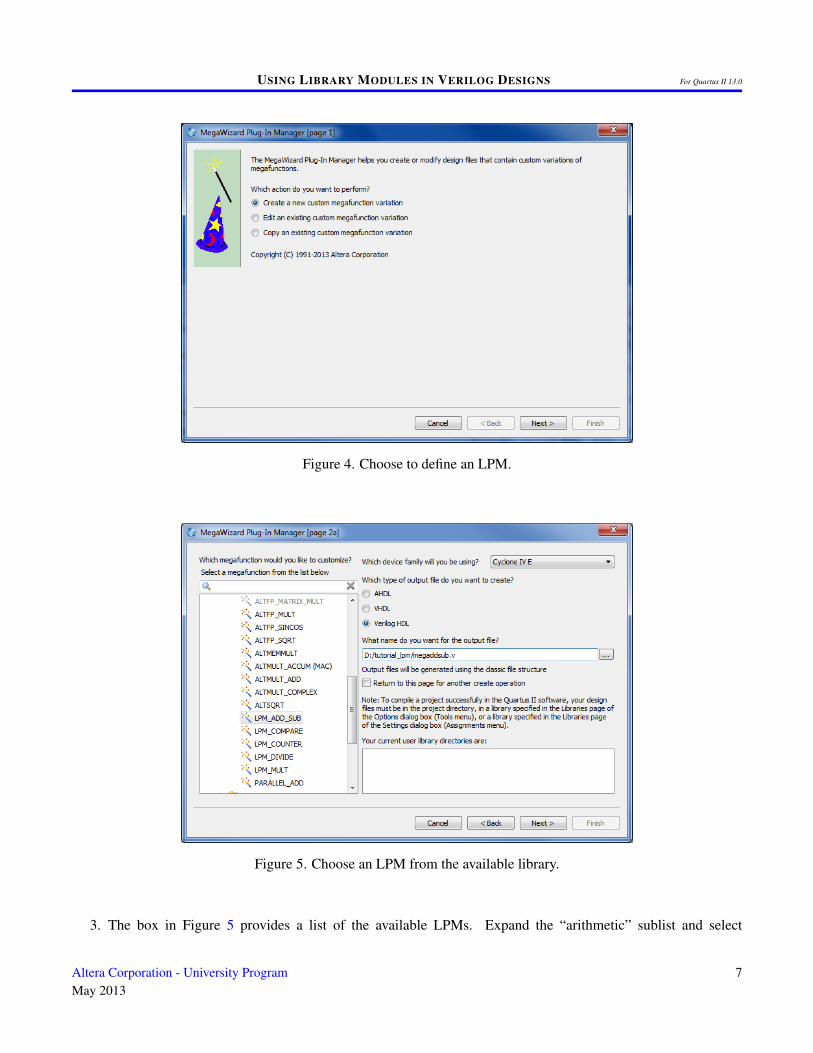
1. Select Tools > MegaWizard Plug-in Manager, which leads to a sequence of seven pop-up boxes in whichthe user can specify the details of the desired LPM.
2. In the box shown in Figure 4 indicate Create a new custom megafunction variation and click Next.
6 Altera Corporation - University ProgramMay 2013
USING LIBRARY MODULES IN VERILOG DESIGNS For Quartus II 13.0
Figure 4. Choose to define an LPM.
Figure 5. Choose an LPM from the available library.
3. The box in Figure 5 provides a list of the available LPMs. Expand the “arithmetic” sublist and select
Altera Corporation - University ProgramMay 2013
7

USING LIBRARY MODULES IN VERILOG DESIGNS For Quartus II 13.0
LPM_ADD_SUB. Choose Verilog HDL as the type of output file that should be created. The output filemust be given a name; choose the name megaddsub.v and indicate that the file should be placed in the direc-tory tutorial_lpm as shown in the figure. Press Next.
Figure 6. Specify the size of data inputs.
4. In the box in Figure 6 specify that the width of the data inputs is 16 bits. Also, specify the operating modein which one of the ports allows performing both addition and subtraction of the input operand, under thecontrol of the add_sub input. A symbol for the resulting LPM is shown in the top left corner. Note that ifadd_sub = 1 then result = A +B ; otherwise, result = A −B . This interpretation of the control input and theoperation performed is different from our original design in Figures 1 and 2, which we have to account for inthe modified design. Observe that we have included this change in the circuit in Figure 3. Click Next.
8 Altera Corporation - University ProgramMay 2013

USING LIBRARY MODULES IN VERILOG DESIGNS For Quartus II 13.0
Figure 7. Further specification of inputs.
5. In the box in Figure 7, specify that the values of both inputs may vary and select Signed for the type ofaddition/subtraction. Click Next.
Altera Corporation - University ProgramMay 2013
9
USING LIBRARY MODULES IN VERILOG DESIGNS For Quartus II 13.0
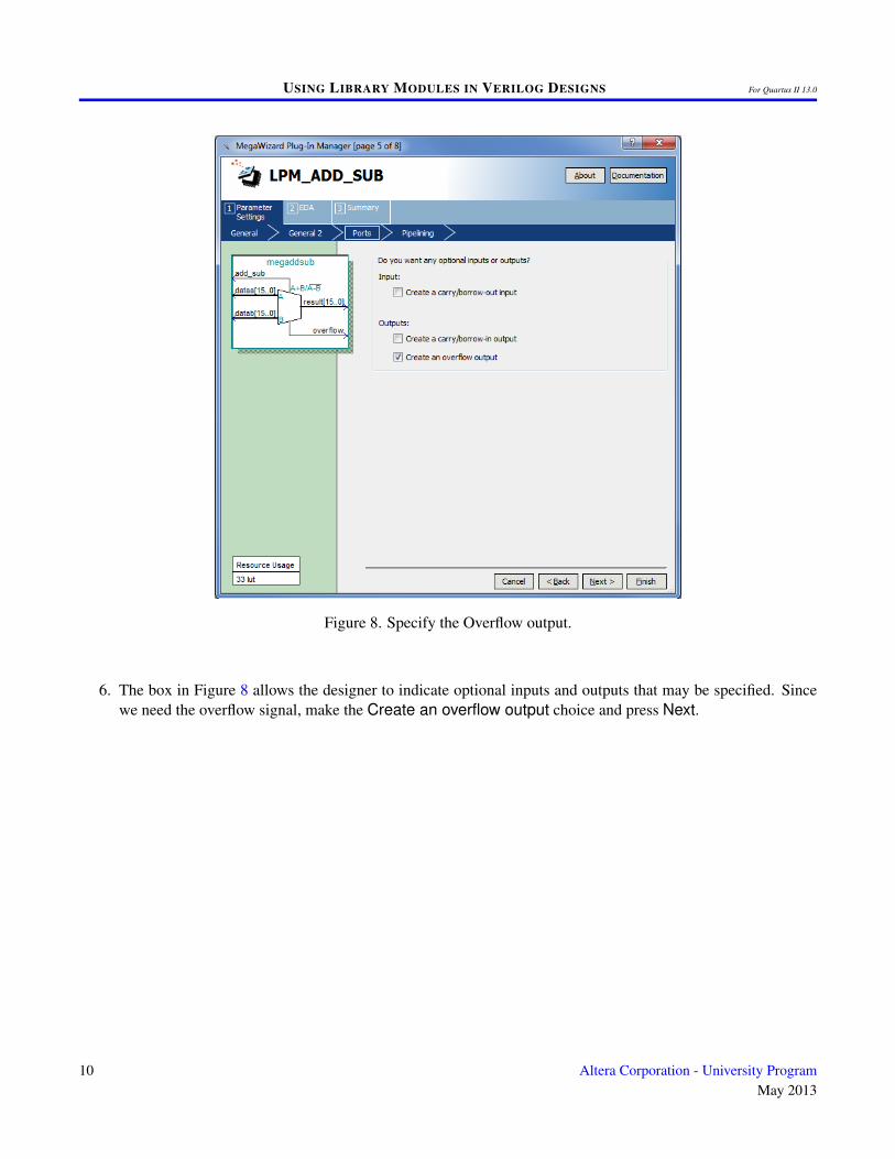
Figure 8. Specify the Overflow output.
6. The box in Figure 8 allows the designer to indicate optional inputs and outputs that may be specified. Sincewe need the overflow signal, make the Create an overflow output choice and press Next.
10 Altera Corporation - University ProgramMay 2013
USING LIBRARY MODULES IN VERILOG DESIGNS For Quartus II 13.0
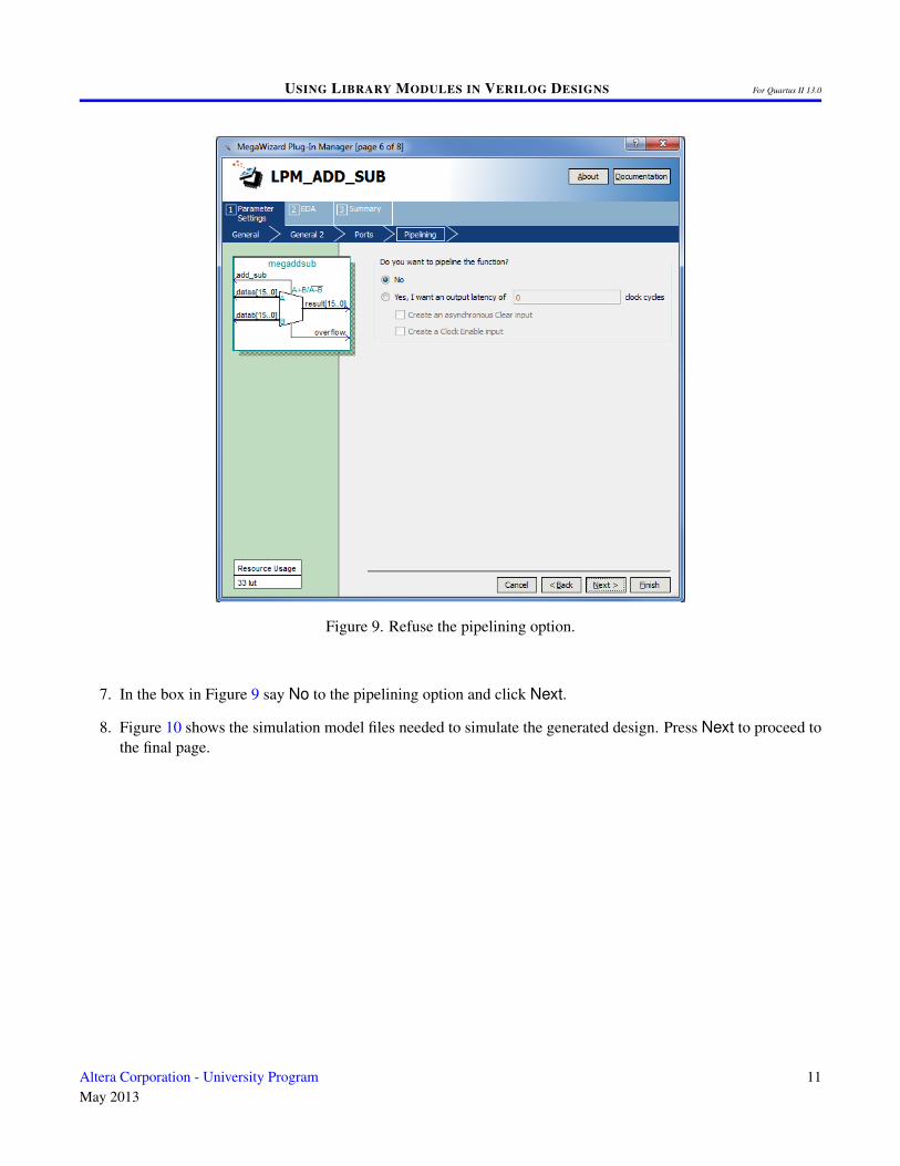
Figure 9. Refuse the pipelining option.
7. In the box in Figure 9 say No to the pipelining option and click Next.
8. Figure 10 shows the simulation model files needed to simulate the generated design. Press Next to proceed tothe final page.
Altera Corporation - University ProgramMay 2013
11

USING LIBRARY MODULES IN VERILOG DESIGNS For Quartus II 13.0
Figure 10. Simulation model files.
9. Figure 11 gives a summary which shows the files that the wizard will create. Press Finish to complete theprocess.
12 Altera Corporation - University ProgramMay 2013

USING LIBRARY MODULES IN VERILOG DESIGNS For Quartus II 13.0
Figure 11. Files created by the wizard.
10. The box in Figure 12 may pop up. If it does, press Yes to add the newly generated files to the project.
Figure 12. Add the new files to the project.
Altera Corporation - University ProgramMay 2013
13

USING LIBRARY MODULES IN VERILOG DESIGNS For Quartus II 13.0
5 Augmented Circuit with an LPM
We will use the file megaddsub.v in our modified design. Figure 13 depicts the Verilog code in this file; note that wehave not shown the comments in order to keep the figure small.
// Adder/subtractor module created by the MegaWizardmodule megaddsub (
add_sub,dataa,datab,overflow,result);
input add_sub;input [15:0] dataa;input [15:0] datab;output overflow;output [15:0] result;wire sub_wire0;wire [15:0] sub_wire1;wire overflow = sub_wire0;wire [15:0] result = sub_wire1[15:0];
lpm_add_sub lpm_add_sub_component (.dataa (dataa),.add_sub (add_sub),.datab (datab),.overflow (sub_wire0),.result (sub_wire1));
defparamlpm_add_sub_component.lpm_direction = "UNUSED",lpm_add_sub_component.lpm_hint = "ONE_INPUT_IS_CONSTANT=NO,CIN_USED=NO",lpm_add_sub_component.lpm_representation = "SIGNED",lpm_add_sub_component.lpm_type = "LPM_ADD_SUB",lpm_add_sub_component.lpm_width = 16;
endmodule
Figure 13. Verilog code for the ADD_SUB LPM.
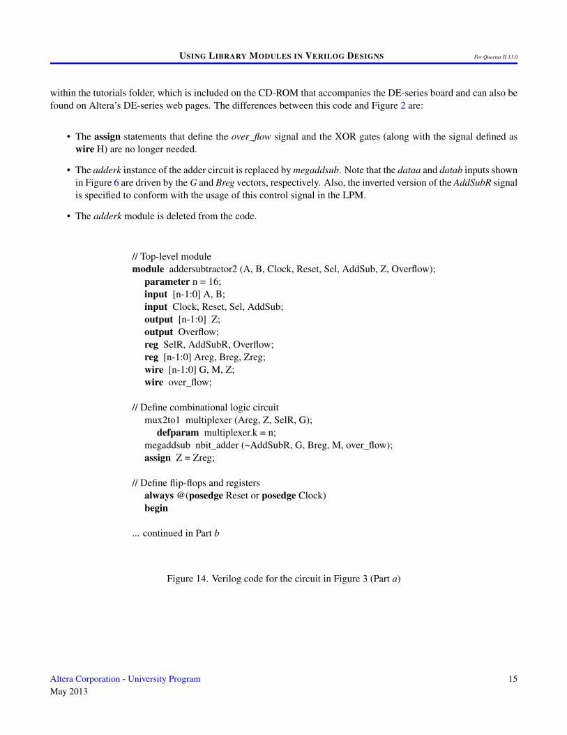
The modified Verilog code for the adder/subtractor design is given in Figure 14. Put this code into a file addersub-tractor2.v under the directory tutorial_lpm. For convenience, this file is provided in the design_files subdirectory
14 Altera Corporation - University ProgramMay 2013
USING LIBRARY MODULES IN VERILOG DESIGNS For Quartus II 13.0
within the tutorials folder, which is included on the CD-ROM that accompanies the DE-series board and can also befound on Altera’s DE-series web pages. The differences between this code and Figure 2 are:
• The assign statements that define the over_flow signal and the XOR gates (along with the signal defined aswire H) are no longer needed.
• The adderk instance of the adder circuit is replaced by megaddsub. Note that the dataa and datab inputs shownin Figure 6 are driven by the G and Breg vectors, respectively. Also, the inverted version of the AddSubR signalis specified to conform with the usage of this control signal in the LPM.
• The adderk module is deleted from the code.
// Top-level modulemodule addersubtractor2 (A, B, Clock, Reset, Sel, AddSub, Z, Overflow);
parameter n = 16;input [n-1:0] A, B;input Clock, Reset, Sel, AddSub;output [n-1:0] Z;output Overflow;reg SelR, AddSubR, Overflow;reg [n-1:0] Areg, Breg, Zreg;wire [n-1:0] G, M, Z;wire over_flow;
// Define combinational logic circuitmux2to1 multiplexer (Areg, Z, SelR, G);
defparam multiplexer.k = n;megaddsub nbit_adder (~AddSubR, G, Breg, M, over_flow);assign Z = Zreg;
// Define flip-flops and registersalways @(posedge Reset or posedge Clock)begin
... continued in Part b
Figure 14. Verilog code for the circuit in Figure 3 (Part a)
Altera Corporation - University ProgramMay 2013
15

USING LIBRARY MODULES IN VERILOG DESIGNS For Quartus II 13.0
if (Reset == 1)begin
Areg <= 0; Breg <= 0; Zreg <= 0;SelR <= 0; AddSubR <= 0; Overflow <= 0;
endelsebegin
Areg <= A; Breg <= B; Zreg <= M;SelR <= Sel; AddSubR <= AddSub; Overflow <= over_flow;
endend
endmodule// k-bit 2-to-1 multiplexermodule mux2to1 (V, W, Selm, F);
parameter k = 8;input [k-1:0] V, W;input Selm;output [k-1:0] F;reg [k-1:0] F;always @(V or W or Selm)
if (Selm == 0)F = V;
elseF = W;
endmodule
Figure 14. Verilog code for the circuit in Figure 3 (Part b).
If the megaddsub.v file has not been included in the project (e.g. if you answered No in the box in Figure 12, orpossibly if the box did not show up at all), you need to include it manually. To include the megaddsub.v file in theproject, select Project > Add/Remove Files in Project to reach the window in Figure 15. The file addersubtrac-tor2.v should already be listed as being included in the project. Browse for the other files by clicking the buttonFile name: ... to reach the window in Figure 16. Select the file megaddsub.v and click Open, which returns to thewindow in Figure 15. Click Add to include the file and then click OK. Now, the modified design can be compiledand simulated in the usual way.
16 Altera Corporation - University ProgramMay 2013

USING LIBRARY MODULES IN VERILOG DESIGNS For Quartus II 13.0
Figure 15. Inclusion of the new file in the project.
Altera Corporation - University ProgramMay 2013
17

USING LIBRARY MODULES IN VERILOG DESIGNS For Quartus II 13.0
Figure 16. Specify the megaddsub.v file.
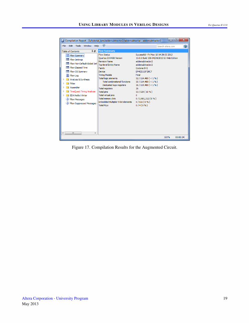
6 Results for the Augmented Design
Compile the design and look at the summary, which is depicted in Figure 17. Observe that the modified design isimplemented with a similar number of logic elements compared to using the code in Figure 2.
18 Altera Corporation - University ProgramMay 2013
USING LIBRARY MODULES IN VERILOG DESIGNS For Quartus II 13.0
Figure 17. Compilation Results for the Augmented Circuit.
Altera Corporation - University ProgramMay 2013
19
USING LIBRARY MODULES IN VERILOG DESIGNS For Quartus II 13.0
Copyright ©1991-2013 Altera Corporation. All rights reserved. Altera, The Programmable Solutions Company, thestylized Altera logo, specific device designations, and all other words and logos that are identified as trademarksand/or service marks are, unless noted otherwise, the trademarks and service marks of Altera Corporation in theU.S. and other countries. All other product or service names are the property of their respective holders. Alteraproducts are protected under numerous U.S. and foreign patents and pending applications, mask work rights, andcopyrights. Altera warrants performance of its semiconductor products to current specifications in accordance withAltera’s standard warranty, but reserves the right to make changes to any products and services at any time withoutnotice. Altera assumes no responsibility or liability arising out of the application or use of any information, product,or service described herein except as expressly agreed to in writing by Altera Corporation. Altera customers areadvised to obtain the latest version of device specifications before relying on any published information and beforeplacing orders for products or services.
This document is being provided on an “as-is” basis and as an accommodation and therefore all warranties, repre-sentations or guarantees of any kind (whether express, implied or statutory) including, without limitation, warrantiesof merchantability, non-infringement, or fitness for a particular purpose, are specifically disclaimed.
20 Altera Corporation - University ProgramMay 2013