using hot wire and initiated chemical vapor deposition for ...purl.tue.nl/387098294720786.pdf ·...
TRANSCRIPT
Thin Solid Films xxx (2014) xxx–xxx
TSF-33793; No of Pages 5
Contents lists available at ScienceDirect
Thin Solid Films
j ourna l homepage: www.e lsev ie r .com/ locate / ts f
Using hot wire and initiated chemical vapor deposition for gas barrierthin film encapsulation
D.A. Spee ⁎, J.K. Rath, R.E.I. Schropp 1
Physics of Devices, Debye Institute for Nanomaterials Science, Utrecht University, High Tech Campus, Building 21, 5656 AE Eindhoven, The Netherlands
⁎ Corresponding author at: Roth&RauB.V., LuchthavenNetherlands. Tel.: +31 40 2581715.
E-mail address: [email protected] (D.A. Spee)1 Present address: Energy Centre of the Netherlands (EC
21, 5656 AE Eindhoven, The Netherlands; EindhoveDepartment of Applied Physics, P.O. Box 513, 5600 MB Ei
http://dx.doi.org/10.1016/j.tsf.2014.10.0290040-6090/© 2014 Elsevier B.V. All rights reserved.
Please cite this article as: D.A. Spee, et al., UsinFilms (2014), http://dx.doi.org/10.1016/j.tsf.
a b s t r a c t
a r t i c l e i n f oAvailable online xxxx
Keywords:HWCVDiCVDPermeation barrierOrganic/inorganic multilayer
Hotwire CVD (HWCVD) and initiated CVD (iCVD) are verywell suited deposition techniques for the fabrication oftransparent thin film gas barriers. Single inorganic or organic layers, however, face challenges, which are hard toovercome: unavoidable defects and low intrinsic barrier function. We demonstrate that by combining inorganicHWCVD films and organic iCVD films, a water vapor transmission rate a low as 5 ∗ 10−6 g/m2/day at 60 °C and90% RH for a simple pinhole free three layer structure is obtained even with non-optimized individual layers.Given the 100 °C deposition temperature, the layer stacks can be deposited on any sensitive electronic device.
© 2014 Elsevier B.V. All rights reserved.
1. Introduction
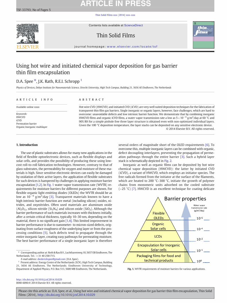
The use of plastic substrates allows for many new applications in thefield of flexible optoelectronic devices, such as flexible displays andsolar cells, and provides the possibility of producing these using low-cost roll-to-roll fabrication technologies. However, contrary to that ofglass substrates, the permeability for oxygen andmoisture of these ma-terials is high. Since sensitive electronic devices can easily be damagedby oxidation of their active layers, the application of flexible substratesfor such devices is hampered by challenges in applyingmoisture barrierencapsulation [1,2]. In Fig. 1 water vapor transmission rate (WVTR) re-quirements for moisture barriers for different purposes are shown. Forflexible organic light emitting diodes (OLEDs) the WVTR should be aslow as 10−6 g/m2/day [3]. Transparent materials known to have ahigh intrinsic barrier function are metal (including silicon) oxides, ni-trides, and oxynitrides. Often used materials are aluminum oxide(Al2O3), silicon nitride (Si3N4) and silicon oxide (SiO2). Although thebarrier performance of suchmaterials increases with thickness initially,after a certain critical thickness, typically 10–30 nm, depending on thematerial, there is no significant gain [1,4]. This limited improvement inbarrier performance is due to nanometer- to micron-sized defects, orig-inating from surface roughness of the underlying layer or from the pro-cessing conditions [5]. Such defects tend to propagate through theentire inorganic layer, creating easy pathways for permeatingmoisture.The best barrier performance of a single inorganic layer is therefore
weg10, 5657 EBEindhoven, The
.N), High Tech Campus, Buildingn University of Technology,ndhoven, The Netherlands.
g hotwire and initiated chem2014.10.029
several orders of magnitude short of the OLED requirements [6]. Toovercome this, multiple inorganic layers can be combined with organic,defect decoupling interlayers, preventing the propagation of perme-ation pathways through the entire barrier [3]. Such a hybrid layerstack is schematically depicted in Fig. 2.
Inorganic as well as organic films can be deposited by hot wirechemical vapor deposition (HWCVD): the latter by initiated CVD(iCVD), a variant of HWCVD, which employs an initiator species. Thefree radicals formed from the initiator at the surface of the filaments,which are heated to 200 °C–300 °C, initiate the growth of polymerchains from monomeric units adsorbed on the cooled substrate(~25 °C) [7]. HWCVD is an excellent technique for coating delicate
Fig. 1. WVTR requirements of moisture barriers for various applications.
ical vapor deposition for gas barrier thin film encapsulation, Thin Solid

Fig. 2. Schematic representation of defect decoupling by organic interlayers.
2 D.A. Spee et al. / Thin Solid Films xxx (2014) xxx–xxx
substrates such as cheap plastics, since precursor decomposition is re-mote from the substrate and no plasma is involved, avoiding high sub-strate temperature and ion bombardment. The continuous HWCVDprocess can easily be implemented in a roll-to-roll or in-line processand since the wires provide a linear source of radicals, the depositedlayers are homogenous in two dimensions, when the substrate ismoved perpendicular to thewires [8]. Giving an overview of results dem-onstrated in the field of thin film gas barriers using HWCVD as well asiCVD, for inorganic and respectively organic coatings, this paper willconclude by addressing our super barrier results combining HWCVDdeposited SiNx with iCVD deposited poly(glycidyl methacrylate)(PGMA) [9] and explaining these in terms of the general strength ofits concept.
2. Inorganic barriers by HWCVD
2.1. Single layer inorganic barriers
One of the most extensively researched inorganic materials for theuse in thin film gas barriers is SiNx, since it has a high intrinsic barrierfunction due to its high density and at the same time it is highly transpar-ent in the visible spectrum. Furthermore, there is no reactive oxygenpresent during its deposition, which avoids the risk of oxidation [1]. Itcan be deposited by HWCVD using SiH4 and NH3 as precursor gasses.Heya et al. [10] used a HWCVD roll-to-roll setup to coat a PET foil withSiNx at substrate temperatures between 20 and 100 °C, obtaining aWVTR of 0.01 g/m2/day for a 40 nm layer. To check its reliability overtime, this barrier was applied to an OLED, which is shown in Fig. 3a. Nodark spots appeared up to 400 h in a 60 °C and 90% relative humidity(RH) environment, corresponding to 5600 h in normal environment[10]. Nakayama and Ito [11] used monomethylsilane (Si(CH3)H3), NH3
and H2 as precursor gases to deposit HWCD SiCN, a material which canbe considered an alloy of SiCx, SiNx and CNx, on a PEN foil as a moisturebarrier. In their studies, it was found to be crucial to coat both sides ofthe PEN film to avoid breakdown of the SiCN/PEN interface due to H2Oaccumulation. Using two 100 nm layers, a WVTR below 10−3 g/m2/daywas obtained. They were able to demonstrate roll-to-roll deposition ofsuch layers on foils up to 75 cmwide.
Fig. 3. a) A flexible OLED covered by a roll-to-roll HWCVD deposited SiNx coated PET film by
Please cite this article as: D.A. Spee, et al., Using hotwire and initiated chemFilms (2014), http://dx.doi.org/10.1016/j.tsf.2014.10.029
2.2. Inorganic multilayer barriers
Ogawa et al. [12] deposited SiOxNy using SiH4, NH3 and O2 as sourcegases. Although the WVTR rate of single layers was found to be around3 g/m2/day, the WVTR greatly improved when the SiOxNy layer wasstacked upon SiNx layers. The double layer showed a WVTR of0.018 g/m2/day, one order of magnitude lower than that of a singlelayer of SiNx. This remarkable improvement is ascribed to coverage ofthe cracks in the underlying SiNx layer: since SiOxNy is less dense andmore flexible, no cracks are present in the material, which can be seenin Fig. 3(b). Using 7 of these stacks, an OLED was coated, resulting in1000 h without observing damage, in a 60 °C and 90% RH environment[12]. A new strategy to prevent defects propagation through a barrierstructure is proposed by Majee et al. [13]. Low T silicon nitride layersare stacked, while using an Ar-plasma surface treatment between sub-sequent depositions. Such defect decoupling, without an actual physicalinterlayer, results in a WVTR of 7 ∗ 10−3 g/m2/day for a 250 nm thickbarrier [13].
3. Organic layers by iCVD for barrier coatings
3.1. Organic single layer barriers by iCVD
Organic coatings generally have a high flexibility and the structuraldefects originating from the substrate or underlying layer do not tendto propagate through them. They lack however the hardness and highgas impermeability of inorganic materials. Xu et al. [14] showed thatby increasing the amount of crosslinking in polymer layers themechan-ical properties like hardness and barrier function can be enhanced andbrought more close to that of inorganic materials. Utilizing the mono-mers 4-aminostyrene (4-AS) andmaleic anhydride (Ma), an alternatingcopolymer, PASMa, was deposited by iCVD. After annealing, an ex-tremely high cross-linked polymer was formed, with high mechanicalhardness and barrier properties, while retaining flexibility. The oxygenpermeability of a 25 μm thick polydimethylsiloxane (PDMS)membranewas reduced by 7 orders of magnitude, after coating it with a 200 nmPASMa layer [14]. Although this is a very promising result the high in-trinsic permeability of polymers remains a challenge to overcome.A more obvious application for polymer layers by iCVD is that ofdecoupling layer in a hybrid multilayer structure.
3.2. Organic layers by iCVD in hybrid barriers
Good performance of a hybrid multilayer can be ascribed to the tor-tuous path that permeating molecules must follow through the organiclayer between pinholes in consecutive inorganic layers [15]. This effectdepends on small organic interlayer thickness. As soon as the interlayerthickness becomes less than the average lateral distance betweendefects in consecutive inorganic layers, the diffusion of permeating
Heya et al. [10]. b) Cross section SEM image of a SiNx/SiOxNy stack by Ogawa et al. [13].
ical vapor deposition for gas barrier thin film encapsulation, Thin Solid

Fig. 4. a) The moisture diffusion rate is dependent on the ratio of the lateral distance between defects in the consecutive layer and the interlayer thickness. A theoretical ideal structure isdepicted [1]. b) Layers by iCVD are excellent planarizing layers, even at small thickness. The rms roughness of an Asahi substrate was reduced from 42.3 nm to 14.3 nmwith a planarizingPGMA layer of 335 nm [21]. c) Schematic representation of the filling of nanopores in the inorganic layer by monomers and the subsequent polymerization in the iCVD process [17].
3D.A. Spee et al. / Thin Solid Films xxx (2014) xxx–xxx
molecules is slowed down significantly [1]. This is shown in Fig. 4(a).iCVD allows for the deposition of films with nanoscale thicknesseswith macroscale uniformity, making it very well suited to deposit suchinterlayers [16]. Using iCVD to deposit the interlayers brings additionalbarrier enhancement: It was shown by Aresta et al. [17], that in casenanopores are present in the inorganic material, deposited iCVD layersare very effective in filling them, as it is schematically depicted inFig. 4(c). In addition to permeation through macroscopic defects, per-meation through these nano-scale defects in the inorganic matrixplays an important role in the permeation barrier characteristics [18].Smoothening of the underlying surface to avoid defect formation ingrowing inorganic layers is a third important property of the organic in-terlayer [19]. Bakker et al. [20] showed that iCVD deposited layers arevery suitable as planarization layers, even at small thicknesses. Theysucceeded in planarizing a rough Asahi U-type TCO substrate by a335 nm iCVD PGMA layer, reducing the rms roughness form 42 nm to14 nm, as shown in Fig. 4(b). It was confirmed by Coclite and Gleason[21] that the barrier performance of a 20-nm SiOx layer on a PET sub-strate was increased by two orders of magnitude when an iCVD depos-ited planarizing layer was applied first. The same group was the first
Fig. 5. a) A hybrid organic/inorganicmultilayer barrier, deposited by Coclite and Gleason, with aber of PECVD layers.
Please cite this article as: D.A. Spee, et al., Using hotwire and initiated chemFilms (2014), http://dx.doi.org/10.1016/j.tsf.2014.10.029
utilizing organic layers by iCVD as interlayers in a hybrid barrier withPECVD deposited oxide layers [22]. An inorganic/organic multilayerwas deposited in a single deposition chamber using one single precur-sor, hexavinyldisiloxane (HVDSO). Using iCVD, organic layers were de-posited, whereas using PECVD, precursor fragmentation resulted in aSiOx-like inorganic layer. By depositing the inorganic layer on top of theiCVD layers using PECVD, hereby exposing it to ion bombardment, agraded barrier was formed, avoiding adhesion challenges at an organic/inorganic interface [22]. Coating a PEN substrate with a hexalayer, aWVTR of 0.01 g/m2/day was achieved (Fig. 5).
4. Compatibility of HWCVD and iCVD deposited materials
To be able to deposit inorganic materials on top of the iCVD layers,there are some requirement for individual materials and their deposi-tion methods. Although HWCVD is in nature a very gentle depositiontechnique, the substrate can be heated significantly by radiation fromthewires, damaging delicate organic layers.Whereas in roll-to-roll pro-cesses this should not be a problem, due to easy cooling of the substrate,in a batch type small R&D vacuum deposition system cooling is more
combined iCVD/PECVD approach using one precursor [22]. b)WVTR as a function of num-
ical vapor deposition for gas barrier thin film encapsulation, Thin Solid
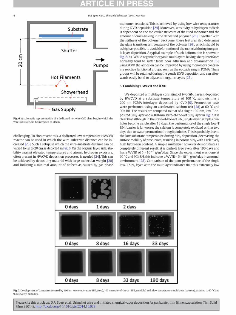
Fig. 6. A schematic representation of a dedicated hot wire CVD chamber, in which thewire-substrate can be increased to 20 cm.
4 D.A. Spee et al. / Thin Solid Films xxx (2014) xxx–xxx
challenging. To circumvent this, a dedicated low temperature HWCVDreactor can be used in which the wire-substrate distance can be in-creased [23]. Such a setup, in which the wire-substrate distance can bevaried to up to 20 cm, is depicted in Fig. 6. On the organic layer side, sta-bility against elevated temperatures and atomic hydrogen exposure,often present in HWCVD deposition processes, is needed [24]. This canbe achieved by depositing material with large molecular weight [20]and inducing a minimal amount of defects as caused by gas phase
Fig. 7.Development of Ca squares covered by100 nm low temperature SiNx (top), 100 nmstate-90% relative humidity.
Please cite this article as: D.A. Spee, et al., Using hotwire and initiated chemFilms (2014), http://dx.doi.org/10.1016/j.tsf.2014.10.029
monomer reactions. This is achieved by using low wire temperaturesduring iCVD deposition [24]. Moreover, sensitivity to hydrogen radicalsis dependent on the molecular structure of the used monomer and theamount of cross-linking in the deposited polymer [25]. Together withthe stiffness of the polymer backbone, these features also determinethe glass transition temperature of the polymer [26], which should beas high as possible, to avoid deformation of thematerial during inorgan-ic layer deposition. A typical example of such deformation is shown inFig. 8(b). While organic/inorganic multilayers having sharp interfacesnormally tend to suffer from poor adhesion and delamination [6],using iCVD the adhesion can be improved by using monomers contain-ing reactive functional groups, such as the epoxide ring in PGMA. Thesegroupswill be retained during the gentle iCVD deposition and can after-wards easily bond to adjacent inorganic layers [27].
5. Combining HWCVD and iCVD
We deposited a multilayer consisting of two SiNx layers, depositedby HWCVD at a substrate temperature of 100 °C, sandwiching a200 nm PGMA interlayer deposited by iCVD [9]. Permeation testswere performed using an accelerated calcium test [28] at 60 °C and90% RH. The results are compared to that of a single 100-nm, low-T de-posited SiNx layer and a 100-nm state-of-the-art SiNx layer in Fig. 7. It isclear that although in the state-of-the-art SiNx single-layer samples pin-holes become visible after 16 days, the performance of the single low-TSiNx barrier is far worse: the calcium is completely oxidized within twodays due to water permeation through pinholes. This is probably due tothe low substrate temperature during SiNx deposition, decreasing thesurface mobility of precursors, resulting in porous SiNx with a relativelyhigh hydrogen content. A simple multilayer however demonstrates acompletely different result: it is pinhole free even after 190 days andhas a WVTR of 5 ∗ 10−6 g/m2/day. Since the experiment was done at60 °C and 90%RH, this indicates aWVTR b 5 ∗ 10−7 g/m2/day in a normalenvironment [28]. Comparison of the poor performance of the singlelow-T SiNx layer with the multilayer indicates that this extremely low
of-the-art SiNx (middle) and a low temperaturemultilayer (bottom), exposed to 60 °C and
ical vapor deposition for gas barrier thin film encapsulation, Thin Solid
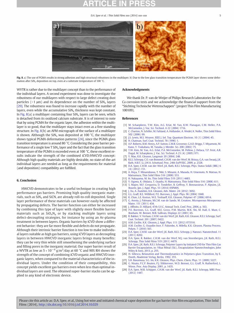
Fig. 8. a) The use of PGMA results in strong adhesion and high structural robustness in the multilayer. b) Due to the low glass transition temperature the PGMA layer shows some defor-mation after SiNx deposition on top, even at a substrate temperature of 100 °C.
5D.A. Spee et al. / Thin Solid Films xxx (2014) xxx–xxx
WVTR is rather due to themultilayer concept than to the performance ofthe individual layers. A second experiment was done to investigate therobustness of our multilayers with respect to large defect creating dustparticles (N1 μm) and its dependence on the number of SiNx layers[29]. The robustness was found to increase rapidly with the number oflayers, even while the accumulative SiNx thickness was kept constant.In Fig. 8(a) a multilayer containing four SiNx layers can be seen, whichis detached from its oxidized calcium substrate. It is of interest to notethat by using PGMA for the organic layer, the adhesion within themulti-layer is so good, that the multilayer stays intact even as a free standingstructure. In Fig. 8(b) an AFM micrograph of the surface of a multilayeris shown. Although the SiNx was deposited at 100 °C, the multilayershows typical PGMA deformation patterns [24], since the PGMA glasstransition temperature is around 80 °C. Considering the poor barrier per-formance of a single low T SiNx layer and the fact that the glass transitiontemperature of the PGMA is exceeded even at 100 °C, these excellent re-sults indicate the strength of the combined iCVD/HWCVD concept:Although high quality materials are highly desirable, no state-of-the-artindividual layers are needed as long as the requirements for material(and deposition) compatibility are fulfilled.
6. Conclusion
HWCVD demonstrates to be a useful technique in creating highperformance gas barriers. Promising high quality inorganic mate-rials, such as SiNx and SiCN, are already roll-to-roll deposited. Singlelayer performance of these materials can however easily be affectedby propagating defects. The barrier function can either be increasedby combining this type of layer with slightly more flexible barriermaterials such as SiOxNy or by stacking multiple layers usingdefect-decoupling strategies, for instance by using an Ar-plasmatreatment in between layers. Organic barriers by iCVD show a differ-ent behavior: they are far more flexible and defects do not propagate.Although their intrinsic barrier function is too low to make individu-al layers suitable as high gas barriers, using iCVD layers as decouplinglayers in between HWCVD inorganic layers brings many benefits:they can be very thin while still smoothening the underlying surfaceand filling pores in the inorganic material. Our super barrier result ofa WVTR as low as 5 ∗ 10−6 g/m2/day at 60 °C and 90% RH shows thestrength of the concept of combining iCVD organic and HWCVD inor-ganic layers, when compared to thematerial characteristics of the in-dividual layers. Under the condition of their compatibility, thisconcept yields excellent gas barriers even when less than optimal in-dividual layers are used. The obtained super-barrier stacks can be ap-plied to any kind of electronic device.
Please cite this article as: D.A. Spee, et al., Using hotwire and initiated chemFilms (2014), http://dx.doi.org/10.1016/j.tsf.2014.10.029
Acknowledgments
We thank Dr. P. van deWeijer of Philips Research Laboratories for theCa corrosion tests and we acknowledge the financial support from the“Stichting TechnischeWetenschappen” (project Thin FilmManufacturing100109).
References
[1] M. Schaepkens, T.W. Kim, A.G. Erlat, M. Yan, K.W. Flanagan, C.M. Heller, P.A.McConnelee, J. Vac. Sci. Technol. A 22 (2004) 1716.
[2] C. Charton, N. Schiller, M. Fahland, A. Hollander, A. Wedel, K. Noller, Thin Solid Films502 (2006) 99.
[3] J.S. Lewis, M.S. Weaver, IEEE J. Sel. Top. Quantum Electron. 10 (1) (2004) 45.[4] H. Chatman, Surf. Coat. Technol. 78 (1996) 1.[5] A.P. Roberts, B.M. Henry, A.P. Sutton, C.M.R. Grovenor, G.A.D. Briggs, T. Miyamoto, M.
Kano, Y. Tsukahara, M. Yanaka, J. Membr. Sci. 208 (2002) 75.[6] T.W. Kim, M. Yan, A.G. Erlat, P.A. McConnelee, M. Pellow, J. Deluca, T.P. Feist, A.R.
Dugal, M. Schaepkens, J. Vac. Sci. Technol. A 23 (4) (2005) 971.[7] Y. Mao, K.K. Gleason, Langmuir 20 (2004) 248.[8] R.E.I. Schropp, C.O. van Bommel, C.H.M. van derWerf, M. Brinza, G.A. van Swaaij, J.K.
Rath, H.B.T. Li, J.W.A. Schuttauf, Proc. 24th EuPVSEC, 2009, p. 2328.[9] D.A. Spee, C.H.M. van der Werf, J.K. Rath, R.E.I. Schropp, Phys. Status Solidi (RRL) 6
(4) (2012) 151.[10] A. Heya, T. Minamikawa, T. Niki, S. Minami, A. Masuda, H. Umemoto, N. Matsuo, H.
Matsumura, Thin Solid Films 516 (2008) 553.[11] H. Nakayama, M. Ito, Thin Solid Films 519 (2011) 4483.[12] Y. Ogawa, K. Ohdaira, T. Oyaidu, H. Matsumura, Thin Solid Films 516 (2008) 611.[13] S. Majee, M.F. Cerqueira, D. Tondelier, B. Geffroy, Y. Bonnassieux, P. Alpuim, J.E.
Bourée, Jpn. J. Appl. Phys. 53 (2014) 05FM05.[14] J. Xu, A. Asatekin, K.K. Gleason, Adv. Mater. 24 (2012) 3692.[15] G.L. Graff, R.E. Williford, P.E. Burrows, J. Appl. Phys. 96 (2004) 1840.[16] K. Chan, L.E. Kostun, W.E. Tenhaeff, K.K. Gleason, Polymer 47 (2006) 6914.[17] G. Aresta, J. Palmans, M.C.M. van de Sande, M. Creatore, Microporous Mesoporous
Mater. 151 (2011) 434.[18] J. Affinito, D. Hilliard, 47th S.V.C. Annual Tech. Conf. Proc, 2004, p. 563.[19] P.E. Burrows, G.L. Graff, M.E. Gross, P.M. Martin, M.K. Shi, M. Hall, E. Mast, C.
Bonham, W. Bennet, M.B. Sullivan, Displays 22 (2001) 65.[20] R. Bakker, V. Verlaan, C.H.M. van derWerf, J.K. Rath, K.K. Gleason, R.E.I. Schropp, Surf.
Coat. Technol. 201 (2007) 9422.[21] A.M. Coclite, K.K. Gleason, J. Appl. Phys. 111 (2012) 073516.[22] A.M. Coclite, G. Ozaydin-Ince, F. Palumbo, A. Milella, K.K. Gleason, Plasma Process.
Polym. 7 (2010) 561.[23] D.A. Spee, C.H.M. van der Werf, J.K. Rath, R.E.I. Schropp, J. Nanosci. Nanotechnol. 11
(2011) 8202.[24] D.A. Spee, R. Bakker, C.H.M. van der Werf, M.J. van Steenbergen, J.K. Rath, R.E.I.
Schropp, Thin Solid Films 519 (2011) 4479.[25] D.A. Spee, J.K. Rath, R.E.I. Schropp, Polymer Layers by Initiated CVD for Thin Film Gas
Barrier Encapsulation, in: Vikas Mittal (Ed.), Encapsulation Nanotechnologies, JohnWiley & Sons, 2013, p. 255.
[26] H. Sillescu, Relaxation and Thermodynamics in Polymers-glass Transition, by E.Donth, Akademie Verlag, Berlin, 1992. 355.
[27] S.H. Baxamusa, S.G. Im, K.K. Gleason, Phys. Chem. Chem. Phys. 11 (2009) 5227.[28] G. Nisato, P.C.P. Bouten, P.J. Slikkerveer, W.D. Bennet, G.L. Graff, N. Rutherford, L.
Wiese, Proc. Asia Display, 2001, p. 1435.[29] D.A. Spee, M.R. Schipper, C.H.M. van der Werf, J.K. Rath, R.E.I. Schropp, MRS Proc.
(2012) 1447.
ical vapor deposition for gas barrier thin film encapsulation, Thin Solid