using gps receiver 1pps output to verify time stamp ... · a pulse overlay (po) circuit was...
TRANSCRIPT

NASA/TM—2019–220231
Using GPS Receiver 1PPS Output to Verify
Time Stamp Accuracy and Measure
Propagation Delay
Kevin Knudtson
Armstrong Flight Research Center
Edwards, California 93523
Antonio Moreno
Arcata Associates, Inc.
Edwards, California 93523
Click here: Press F1 key (Windows) or Help key (Mac) for help
July 2019
https://ntrs.nasa.gov/search.jsp?R=20190028909 2020-04-01T11:38:11+00:00Z

NASA STI Program ... in Profile
Since its founding, NASA has been dedicated
to the advancement of aeronautics and space
science. The NASA scientific and technical
information (STI) program plays a key part in
helping NASA maintain this important role.
The NASA STI program operates under the
auspices of the Agency Chief Information Officer.
It collects, organizes, provides for archiving, and
disseminates NASA’s STI. The NASA STI
program provides access to the NTRS Registered
and its public interface, the NASA Technical
Reports Server, thus providing one of the largest
collections of aeronautical and space science STI
in the world. Results are published in both non-
NASA channels and by NASA in the NASA STI
Report Series, which includes the following report
types:
TECHNICAL PUBLICATION. Reports of
completed research or a major significant
phase of research that present the results of
NASA Programs and include extensive data
or theoretical analysis. Includes compila-
tions of significant scientific and technical
data and information deemed to be of
continuing reference value. NASA counter-
part of peer-reviewed formal professional
papers but has less stringent limitations on
manuscript length and extent of graphic
presentations.
TECHNICAL MEMORANDUM.
Scientific and technical findings that are
preliminary or of specialized interest,
e.g., quick release reports, working
papers, and bibliographies that contain
minimal annotation. Does not contain
extensive analysis.
CONTRACTOR REPORT. Scientific and
technical findings by NASA-sponsored
contractors and grantees.
CONFERENCE PUBLICATION.
Collected papers from scientific and
technical conferences, symposia, seminars,
or other meetings sponsored or
co-sponsored by NASA.
SPECIAL PUBLICATION. Scientific,
technical, or historical information from
NASA programs, projects, and missions,
often concerned with subjects having
substantial public interest.
TECHNICAL TRANSLATION.
English-language translations of foreign
scientific and technical material pertinent to
NASA’s mission.
Specialized services also include organizing
and publishing research results, distributing
specialized research announcements and
feeds, providing information desk and personal
search support, and enabling data exchange
services.
For more information about the NASA STI
program, see the following:
Access the NASA STI program home page
at http://www.sti.nasa.gov
E-mail your question to [email protected]
Phone the NASA STI Information Desk at
757-864-9658
Write to:
NASA STI Information Desk
Mail Stop 148
NASA Langley Research Center
Hampton, VA 23681-2199
This page is required and contains approved text that cannot be changed.

NASA/TM—2019–220231
Using GPS Receiver 1PPS Output to Verify
Time Stamp Accuracy and Measure
Propagation Delay
Kevin Knudtson
Armstrong Flight Research Center
Edwards, California 93523
Antonio Moreno
Arcata Associates, Inc.
Edwards, California 93523
Insert conference information, if applicable; otherwise delete
Click here: Press F1 key (Windows) or Help key (Mac) for help
National Aeronautics and
Space Administration
Armstrong Flight Research Center Edwards, California 93523-0273
July 2019

Enter acknowledgments here, if applicable.
Click here: Press F1 key (Windows) or Help key (Mac) for help
This report is available in electronic form at
http://ntrs.nasa.gov

1
Abstract
A simple pulse overlay circuit using a logic OR gate was developed to overlay a precise leading edge 1 pulse per second time reference marker from a global positioning system receiver onto a non-return -to- zero-level pulse code modulation telemetry data stream to validate time stamp accuracy and measure propagation delay in telemetry equipment.
Nomenclature
BNC Bayonet Neill Concelman connector br PCM data bit rate C capacitor CH channel DA distribution amplifier DAU distribution amplifiers unit Db additional bits offset to the first 1PPS VPW data bit DB packet viewer’s reported byte address nearest to the first 1PPS VPW data bit EI electrical in EO electrical out GPS global positioning system IPH intra-packet data header size = 80 bits OC03 optical carrier level three OS one-shot OI optical in OTDR optical time domain reflectometer OU optical out PCM pulse code modulation PD propagation delay PO pulse overlay PRN11 pseudo random number 11 RTC real time counter RX receive R resistor TX transmit VDA video distribution amplifiers VDC voltage direct current VPW variable pulse width VR1 variable resistor one 1PPS one pulse per second
Introduction
A pulse overlay (PO) circuit was designed to produce a time reference marker within a pulse code modulation (PCM) telemetry data stream that was recorded and analyzed to validate an IRIG Standard 106-17 Chapter 10 recorder’s time stamp accuracy (Ref. 1). A manufacturer of a newly purchased Chapter 10 recorder claimed the time stamp accuracy to be better than 10 microseconds (µs) with only IRIG-B120 [Inter-range instrumentation group, time code format B (IRIG-B)] input and better than 1 µs with IRIG-B and one pulse per second (1PPS) inputs. The PO circuit and a Chapter 10 recorder test setup were used to verify the vendor’s data-time
2
synchronization claims and to justify infrastructure upgrade costs to connect additional cables to each purchased recorder. The circuit was also used to measure the propagation delay (PD) of a long distance Telemetry multiplexer/demultiplexer telecommunication system which the manufacturer did not provide a PD specification.
Circuit Design
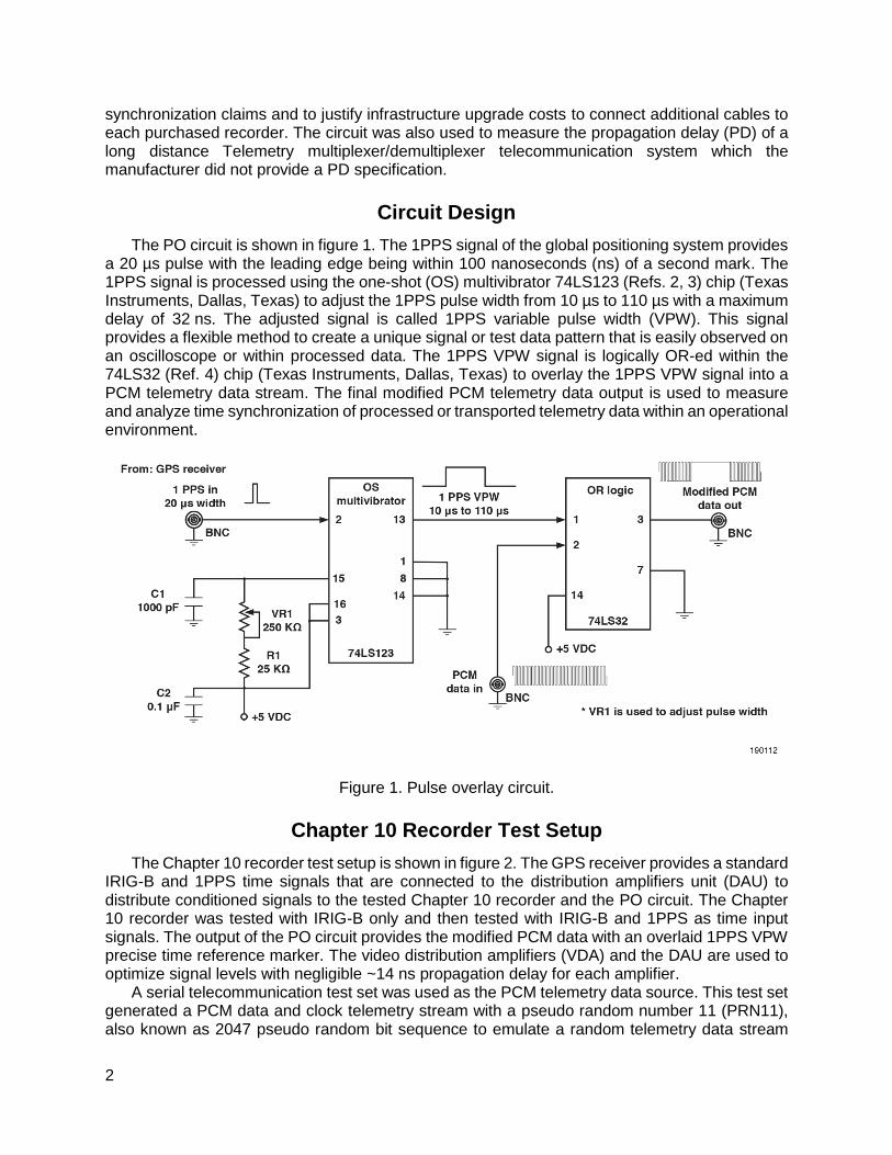
The PO circuit is shown in figure 1. The 1PPS signal of the global positioning system provides a 20 µs pulse with the leading edge being within 100 nanoseconds (ns) of a second mark. The 1PPS signal is processed using the one-shot (OS) multivibrator 74LS123 (Refs. 2, 3) chip (Texas Instruments, Dallas, Texas) to adjust the 1PPS pulse width from 10 µs to 110 µs with a maximum delay of 32 ns. The adjusted signal is called 1PPS variable pulse width (VPW). This signal provides a flexible method to create a unique signal or test data pattern that is easily observed on an oscilloscope or within processed data. The 1PPS VPW signal is logically OR-ed within the 74LS32 (Ref. 4) chip (Texas Instruments, Dallas, Texas) to overlay the 1PPS VPW signal into a PCM telemetry data stream. The final modified PCM telemetry data output is used to measure and analyze time synchronization of processed or transported telemetry data within an operational environment.
Figure 1. Pulse overlay circuit.
Chapter 10 Recorder Test Setup
The Chapter 10 recorder test setup is shown in figure 2. The GPS receiver provides a standard IRIG-B and 1PPS time signals that are connected to the distribution amplifiers unit (DAU) to distribute conditioned signals to the tested Chapter 10 recorder and the PO circuit. The Chapter 10 recorder was tested with IRIG-B only and then tested with IRIG-B and 1PPS as time input signals. The output of the PO circuit provides the modified PCM data with an overlaid 1PPS VPW precise time reference marker. The video distribution amplifiers (VDA) and the DAU are used to optimize signal levels with negligible ~14 ns propagation delay for each amplifier.
A serial telecommunication test set was used as the PCM telemetry data source. This test set generated a PCM data and clock telemetry stream with a pseudo random number 11 (PRN11), also known as 2047 pseudo random bit sequence to emulate a random telemetry data stream

3
(Ref. 5). The PCM clock signal is synchronized to PCM data bits for receiving equipment to correctly process each PCM data bit.
The following is the tested recorder setup: Chapter 10 PCM packet: 16-bit aligned packed mode Bit rate = 2.5 Mb/s PCM sync pattern: 0x805022 Data word length: 12 bits Words/minor frame: 2047 Bits/minor frame; 24576 total = 24564 + 12 filler bits to align data to a 16-bit boundary Minor frames/Chapter 10 PCM packet: 2
Figure 2. Chapter 10 recorder test setup used to verify time stamp accuracy.
Chapter 10 Recorder Time Stamp Offset Test Methodology
A Chapter 10 packet viewer was used to read the recorded Chapter 10 file PCM data in a hex format and to read the time stamp for the first PCM data bit within the packet. The Chapter 10 recorder uses the IRIG-B and optional 1PPS time signals to correlate the Chapter 10 internal 10 MHz relative time counter (RTC) with the on the second IRIG-B time data. The information is recorded within a Chapter 10 time packet. The Chapter 10 recorder then synchronizes PCM data to time by recording an updated RTC value for the first PCM data bit within each PCM packet. One RTC increment represents 100 ns of time. This first PCM data bit time stamp is needed to calculate the time stamp for the first bit of the overlaid 1PPS VPW data sequence.
The packet viewer was also used to find Chapter 10 packets containing and not containing the overlaid 1PPS VPW data sequence. A clean PRN11 sequence data pattern was collected and saved to precisely identify the actual first 1PPS VPW data bit within a Chapter 10 packet. A Chapter 10 packet containing the overlaid 1PPS VPW data sequence will have the first PCM data bit time stamp near a second mark. The displayed PCM data set within the packet viewer was then copied and pasted into a text editor to verify the presence of the unique 1PPS VPW data sequence pattern of “FFF,” (table 1). The clean PRN11 data pattern sequence cannot have more
4
than 11 consecutive 1s, so searching for “FFF” is enough to find the approximate beginning of the full unique 1PPS VPW data pattern.
The main analysis for calculating the time stamp for the first 1PPS VPW data bit is to count the number of bits between the first PCM data bit and the first 1PPS VPW data bit, and divide this count by the PCM bit rate to produce a 1PPS delta time offset that is added to the Chapter 10 first PCM data bit time stamp (see the following formulas for more details).
Table 1. Relationship between 1PPS pulse width and possible hex patterns.
The unique 1PPS VPW signal produces a consecutive 1s data pattern. The relationship between a 1PPS VPW pulse width and PCM bit rate will produce different lengths of consecutive 1s. The consecutive 1s pattern can be viewed as hex and may have possible patterns starting 0x1, 0x3, 0x7, 0xF and ending with 0xE, 0xD, 0xC, or 0x8.
Data rate 1PPS pulse width Number of consecutive 1s bits Example hex patterns
1.0 Mbps 20 µs 20 FFFF F or 1FFF FE or 7FFF F8
2.5 Mbps 20 µs 50 FFFF FFFF FFFF C
4.0 Mbps 20 µs 80 3FFF FFFF FFFF FFFF FFFF C
Formulas to Calculate 1PPS Time Stamp
The following are the variable names and descriptions used in the formulas: 1PPS_time = Calculated time stamp for first bit of 1PPS VPW mF_time = Packet viewer’s reported time stamp for first PCM data bit DB = Packet viewer’s reported byte address nearest to the first 1PPS VPW data bit IPH = Intra-packet data header size = 80 bits Db = Additional bits offset to the first 1PPS VPW data bit Filler = Recorder added bits to end packet on a 16-bit boundary = 12 bits br = PCM data bit rate = 2.5 Mb/s
The setup of the Chapter 10 recorder will record two minor frames of telemetry PCM data within each Chapter 10 PCM packet, so there are 2 formulas to consider in calculating the time stamp of the first 1PPS VPW data bit. The decision point for selecting the correct formula is based on the byte offset for the first 1PPS VPW data bit. If the byte offset is greater than 0x0C0A, Formula 2 accommodates the subtraction of 12 filler bits from the first minor frame and subtracts another 80 IPH bits from the second minor frame. The 0x0C0A decision point is derived from (80 IPH bits + 24,576 bits per minor frame)/8 bits = 3082 bytes = 0x0C0A.
Formula 1 - first bit of 1PPS VPW byte address is “less” than 0x0C0A:
1PPS_time = mF_time + (DB * 8 bits – IPH + Db) / br Formula 2 - first bit of 1PPS VPW byte address is “greater” than 0x0C0A:
1PPS_time = mF_time + (DB * 8 bits – IPH + Db - Filler - IPH) / br
Test 1 Example - Calculated Results with Only IRIG-B Time Input
The analysis example below has its results defined within table 2. The Chapter 10 packet containing the 1PPS VPW data pattern has a time stamp of 077:20:55:03.998354 for the first PCM data bit. The PCM packet data set was copied into a text editor to search for the unique “FFF” data pattern and verify the location of the first 1PPS VPW data bit. The saved standard PRN11 data set was then used to precisely identify the actual first 1PPS VPW data bit (see table 2 for the total of 12 calculated results from this test group).

5
The following shows the values for the variable names used in the formula: mF_time = 077:20:55:03.998354 – Time stamp for first data bit within the PCM packet br = 2.5 Mb/s DB = 0x20A or 522 bytes– Formula 1 used because byte address < 0x0C0A IPH = 80 bits for 16 bit aligned packed mode Db = 0 bit – see packet data below where “FFFF” byte address is 0x20A
Formula 1 is used to calculate the time stamp of the first 1PPS VPW: 1PPS_time = 077:20:55:03.998354 + (522 bytes*8 bits – 80 bits + 0) / 2.5Mbs 1PPS_time = ~077:20:55:03.9999924 = 077:20:55:03.998354 + 0.0016384 First 1PPS VPW data bit time stamp is offset by ~7.6 µs (early) or 19 bits offset
The following shows the shortened Chapter 10 PCM packet data for review:
Packet data: [- intra-packet header (IPH) -] ||-- first PCM data bit is 10002
00000000 E29F 9350 0004 0000 F000 8050 2215 480D
00000010 0723 75D4 50A2 456A 184F 2E72 F725 7615
Byte * Address Normal PRN11 hex sequence:--- 0140 8855 2174 Offset * || 0x20A – bytes offset
00000200 FC61 BCE9 E9C9 DDD5 5002 FFFF FFFF FFFF
00000210 DC8D D751 4289 15A8 613C B9CB DC95 D857
Table 2. Analyzed results of recorded Chapter 10 data with only IRIG-B connected.
Bytes offset hex
Bits offset
First PCM bit time 1pps delta
time, s First 1PPS bit time
Time off, µs
1360 11 077:20:51:29.984184 0.0158076 077:20:51:29.9999916 8.40
0A44 10 077:20:51:59.991612 0.0083816 077:20:51:59.9999936 6.40
0134 0 077:20:52:29.999038 0.0009536 077:20:52:29.9999916 8.40
12DF 0 077:20:52:58.984602 0.0153904 077:20:52:58.9999924 7.60
11E8 3 077:20:53:25.985392 0.0146012 077:20:53:25.9999932 6.80
0C6F 3 077:20:53:57.989874 0.0101180 077:20:53:57.9999920 8.00
0353 0 077:20:54:27.997302 0.0026912 077:20:54:27.9999932 6.80
1249 7 077:20:54:57.985078 0.0149132 077:20:54:57.9999912 8.80
020A 0 077:20:55:03.998354 0.0016384 077:20:55:03.9999924 7.60
092D 3 077:20:55:27.992505 0.0074860 077:20:55:27.9999910 9.00
001C 5 077:20:55:57.999932 0.0000596 077:20:55:57.9999916 8.40
0C60 5 077:20:56:28.989921 0.0100708 077:20:56:28.9999918 8.20
Average time offset 7.87
Test Number 2 Example - Calculated Results with IRIG-B and 1PPS Time Inputs
The analysis example below has its results defined within table 3. The Chapter 10 packet containing the 1PPS VPW data pattern has a time stamp of 077:20:43:55.983476 for the first PCM data bit. The PCM packet data was copied into a text editor to search for the unique “FFF” data pattern and verify the location of the first 1PPS VPW data bit. The saved standard PRN11 data set was then used to better estimate the actual first 1PPS VPW data bit (see table 3 for the total of 12 calculated results from this test group).

6
The following shows the values for the variable names used in the formula: mF_time = 077:20:43:55.983476 – time stamp for first data bit within the PCM packet br = 2.5 Mb/s DB = 0x1441 or 5185 bytes – Formula 2 used because byte address > 0x0C0A IPH = 80 bits for 16 bit aligned packed mode Db = 0 bit– see packet data where “84FF” byte address is 0x1441
Formula 2 is used to calculate the time stamp of first 1PPS VPW:
1PPS_time = 077:20:43:55.983476 + (5185 bytes*8 bits – 80 bits + 0 - 12 bits - 80 bits) /2.5Mb/s 1PPS_time = ~077:20:43:55.9999992= 077:20:43:55.983476 + 0.0165232 First 1PPS VPW data bit time stamp is offset by ~800 ns (early) or 2 bit offset
The following shows the shortened Chapter 10 PCM packet data for review:
Packet data: [-intra-packet header (IPH) -] ||-- first PCM data bit is 10002
00000000 EA31 0525 0003 0000 F000 8050 2215 480D
00000010 0723 75D4 50A2 456A 184F 2E72 F725 7615
Byte address * Address 8472 B70D 671F 6C5B - normal hex sequence Offset * || 0x1441 – bytes offset with first 1PPS data bit is 11112
00001440 84FF FFFF FFFF FFDB A6A7 8733 7FD0 120B
00001450 44CA FC21 94F8 E36D DB56 C1B8 EB68 D977
Table 3. Analyzed results from recorder test with IRIG-B and 1PPS connected.
Bytes offset hex
Bits offset
First PCM bit time 1PPS delta time, s First 1PPS bit time Time off,
µs
08F3 6 077:20:42:57.992699 0.0073016 077:20:42:58.0000006 -0.60
0549 3 077:20:43:25.995701 0.0042988 077:20:43:25.9999998 0.20
1441 0 077:20:43:55.983476 0.0165232 077:20:43:55.9999992 0.80
00FB 0 077:20:44:11.999228 0.0007712 077:20:44:11.9999992 0.80
0B24 5 077:20:44:25.990904 0.0090964 077:20:44:26.0000004 -0.40
0D1D 4 077:20:44:55.989324 0.0106752 077:20:44:55.9999992 0.80
0400 7 077:20:45:25.996752 0.0032476 077:20:45:26. 9999996 0.40
12F8 4 077:20:45:55.984528 0.0154720 077:20:45:56.0000000 -0.00
14E6 1 077:20:46:25.982949 0.0170512 077:20:46:26.0000002 -0.20
0BC9 4 077:20:46:55.990375 0.0096240 077:20:46:55.9999990 1.00
02B8 5 077:20:47:25.997803 0.0021972 077:20:47:26.0000002 -0.20
0759 4 077:20:47:54.994011 0.0059888 077:20:47:54.9999998 0.20
Average time offset 0.23
Summary of Chapter 10 Recorder Test Results
Test results from Chapter 10 recorder test 1 with IRIG-B only has an average offset time of ~7.87 µs (early) and the test results of Chapter 10 recorder test 2 with IRIG-B and 1PPS has an average offset time of ~0.23 µs (late). The two tests successfully verified the vendor’s claim and justified the implementation to add the 1PPS signal to the range Chapter 10 recorders.

7
Propagation Delay Setup and Measurements
The PO circuit was also used to measure the PD of an entire optical carrier level 3 (OC-3) multiplexer/demultiplexer system within its normal operational environment (see figure 3 for test setup). This measurement was needed since the manufacturer did not provide a written PD specification. Using an optical time domain reflectometer (OTDR) would only measure the fiber link.
The test setup with PO circuit provided a simple PD measurement of the entire OC-3 system that included video distribution amplifiers, patch panels, and cables. The 1PPS signal of the GPS receiver provided a solid trigger on the oscilloscope. The oscilloscope cursors were used to measure PD between the sent/return 1PPS VPW signals. The measured PD round-trip was 12.22 milliseconds, which translates to a one-way PD of 6.11 milliseconds. These test results matched with the vendor’s verbal specification of 3 milliseconds PD per OC-3 unit.
Figure 3. Propagation delay measurements block diagram.
Conclusion
Using the one pulse per second time reference marker of the global positioning system receiver and the pulse overlay circuit to overlay the one pulse per second variable pulse width signal into a pulse code modulation telemetry stream provided an excellent means to validate time stamp accuracy within a Chapter 10 recorder and to measure propagation delays within a normal telemetry operating environment. The positive results from the Chapter 10 recorder tests validated the vendor’s claims and justified the implementation to add the one pulse per second signal to the range Chapter 10 recorders. The pulse overlay circuit and test setups defined in this report can easily be used to measure other telemetry equipment.

8
References
1. Telemetry Standards, IRIG Standard 106-17, Range Commanders Council, US Army White Sands Missile Range, New Mexico, Chapter 10, July 2017.
2. Floyd, Thomas L., Digital Fundamentals, 3rd ed., Charles E. Merrill Publishing Company, Columbus, Ohio, 1986.
3. Texas Instruments Incorporated, “Designing with the SN54/74LS123,” Dallas, Texas, 1997, http://www.ti.com/lit/an/sdla006a/sdla006a.pdf, accessed July 10, 2019.
4. Texas Instruments Incorporated, “SN74LS32, Quadruple 2-input positive-Or gates,” Dallas, Texas, December 1983, revised March 1988, http://www.ti.com/lit/ds/sdls 100/ sdls100.pdf, accessed July 10, 2019.
5. International Telecommunication Union, “Digital Test Patterns for Performance Measurements on Digital Transmission Equipment,” O-150, October 1992.