users’manual€¦ · version:v2.0-a2 foreword thank you for purchasing en630/en650a series...
TRANSCRIPT

Users’Manual
Series Inverter
0.4-1.5KW
Ver.2.0
ISO9001 Quality Management System Authentication
CE Authentication
EN630/EN650A series
SHENZHEN ENCOM ELECTRIC TECHNOLOGIES CO.,LTD.

Version:V2.0-A2
Foreword Thank you for purchasing EN630/EN650A series inverter developed and
produced by Shenzhen Encom Electric Technologies CO., LTD.
EN630 series mini hi-performance flux vector inverter adopts advanced control mode to achieve high torque, high precision and wide-range speed regulation drive, and it also supports speed sensorless torque control and PG control torque. It can meet customer all kinds of requirement to universal inverter. EN630 inverter is a organic combination for customer’s universal and industrial control purpose and provides practical main-auxiliary frequency provision, run channel frequency binding, PID regulator, simple PLC, spinning traverse, programmable input&output terminal control, pulse frequency provision and inbuilt Modbus, Can bus, Profibus, RS485 and free protocol and other function and platform. It provides high integration solution for most manufacturing and automation customer and EN630 inbuilt input phase loss function, output phase loss function, short circuit to earth grounding function and many other protective function to improve effectively the system reliability and safety.
EN650A series is a mini multi-function permanent magnet synchronous inverter which combined market demand for synchronous motor and its supporting system, built-in unique control algorithm, can achieve high torque, high precision, wide speed range control for permanent magnet synchronous motor and brushless DC motor, supports PG vector and PG vector control, and also supports speed and torque mode switching.
This brochure provides the installation and wiring settings, fault check and methods, maintenance and other relative issues to customer. To make inverter assemble and operate rightly, and use its high performance to best, please read this brochure carefully before installation usage and keep them well to the final users of inverter.
Please contact our office or dealer anywhere at any moment when you have any doubts or special demands in using these inverters, and you can also contact our after service center in our headquarters directly. We will serve you with all our heart.
We reserve our right to notice you if we change contents of this manual.

Content
Content 1 Safety information and use notice points .............................................................. 1
1.1 Safety precautions .......................................................................................... 1 1.2 Application range ........................................................................................... 3 1.3 Use notice points ............................................................................................ 3
2 Inverter Type and Specification ......................................................................... 5 2.1 Incoming inverter inspect ................................................................................. 5 2.2 Type explanation .............................................................................................. 5 2.3 Nameplate explanation ..................................................................................... 5 2.4 Inverter type explanation .................................................................................. 6 2.5 Appearance and parts name explanation .......................................................... 6 2.6 Outer size & gross weight ................................................................................ 6 2.7 Outer size of keypad and its fixing box ........................................................... 7 2.8 Product technic index and spec ........................................................................ 7
3 Installation and wiring ....................................................................................... 11 3.1 Installation ambient ........................................................................................ 11
3.1.1 The demands for installation ambient ................................................... 11 3.1.2 Installation direction and space ............................................................. 11
3.2 Parts disassembly and installation .................................................................. 12 3.2.1 Keyboard disassembly and installati ..................................................... 12 3.2.2 Plastic cover disassembly and installation ............................................ 12
3.3 Wiring notice points ....................................................................................... 12 3.4 Main loop terminal wiring .............................................................................. 13
3.4.1 Connection between inverter and fitting parts ...................................... 14 3.4.2 Main loop terminal wiring .................................................................... 15
3.5 Basic running wiring diagram ........................................................................ 15 3.6 Control loop collocation and wiring .............................................................. 16
3.6.1 Relative location and function for control board terminal and slide Switch ................................................................................................... 16
3.6.2 Descriptions for control board terminal ................................................ 17 3.6.3 Analog input & output terminal wiring ................................................ 20 3.6.4 Communication terminal wiring ........................................................... 21
3.7 Installation guidance of anti-interference ....................................................... 22 3.7.1 Noise interference restraining ............................................................... 22 3.7.2 Field wiring and earth grounding .......................................................... 24 3.7.3 Long distance wiring & Leak current and countermeasure .................. 25

Content
3.7.4 Installation demand for electromagnetic on-off electronic device .................................................................................................... 25
4 Run and operation explanation for inverter ................................................... 26 4.1 Run of inverter ................................................................................................ 26
4.1.1 Running order channels ........................................................................ 26 4.1.2 Frequency-provision channel ................................................................ 26 4.1.3 Work state ............................................................................................. 27 4.1.4 Run mode .............................................................................................. 27
4.2 Operation and use of key board...................................................................... 29 4.2.1 Keypad layout ....................................................................................... 29 4.2.2 Keypad function description ................................................................. 30 4.2.3 LED and indicator light ......................................................................... 31 4.2.4 Key board display status ....................................................................... 31 4.2.5 User Management Parameters .............................................................. 34 4.2.6 Method for operating keypad ................................................................ 34
4.3 Inverter electrification .................................................................................... 37 4.3.1 Check before electrification .................................................................. 37 4.3.2 First electrification ................................................................................ 37
5 Function Parameter Schedule Graph .............................................................. 39 5.1 Symbol description ......................................................................................... 39 5.2 Function parameter schedule graph ............................................................... 39
6 Troubleshooting .................................................................................................. 84 6.1 Failure and countermeasure ........................................................................... 84 6.2 Failure record lookup ..................................................................................... 90 6.3 Failure reset .................................................................................................... 91 6.4 Alarm reset ..................................................................................................... 91
7 Maintenance ........................................................................................................ 92 7.1 Routine maintenance ...................................................................................... 92 7.2 Inspection and replacement of damageable parts .......................................... 92 7.3 Repair guarantee ............................................................................................. 93 7.4 Storage ............................................................................................................ 93
Appendix A EN650A Mini multi-function PMSM Inverter ................................ 94 Appendix B Free-port Communication Protocol ................................................ 132 Appendix C Modbus communication protocol ................................................... 148 Appendix D Braking unit and braking resistance .............................................. 162
1 Safety information and use notice points
1
1 Safety information and use notice points
To make ensure personal & equipment safety, This chapter must be read carefully before the inverter come into use.
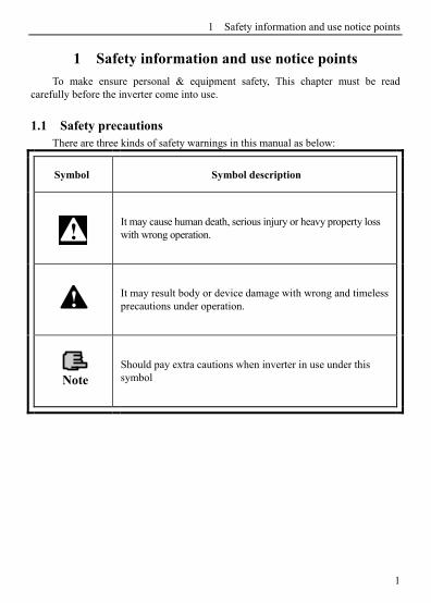
1.1 Safety precautions There are three kinds of safety warnings in this manual as below:
Symbol Symbol description
It may cause human death, serious injury or heavy property loss with wrong operation.
It may result body or device damage with wrong and timeless precautions under operation.
Should pay extra cautions when inverter in use under this symbol
!
Note
!
1 Safety information and use notice points
2
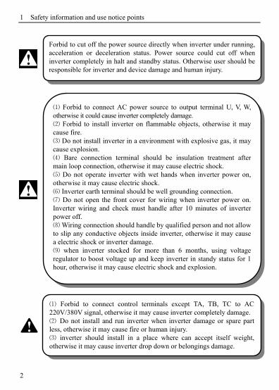
Forbid to cut off the power source directly when inverter under running, acceleration or deceleration status. Power source could cut off when inverter completely in halt and standby status. Otherwise user should be responsible for inverter and device damage and human injury.
!
⑴ Forbid to connect control terminals except TA, TB, TC to AC 220V/380V signal, otherwise it may cause inverter completely damage. ⑵ Do not install and run inverter when inverter damage or spare part less, otherwise it may cause fire or human injury. ⑶ inverter should install in a place where can accept itself weight, otherwise it may cause inverter drop down or belongings damage.
!
⑴ Forbid to connect AC power source to output terminal U, V, W, otherwise it could cause inverter completely damage. ⑵ Forbid to install inverter on flammable objects, otherwise it may cause fire. ⑶ Do not install inverter in a environment with explosive gas, it may cause explosion. ⑷ Bare connection terminal should be insulation treatment after main loop connection, otherwise it may cause electric shock. ⑸ Do not operate inverter with wet hands when inverter power on, otherwise it may cause electric shock. ⑹ Inverter earth terminal should be well grounding connection. ⑺ Do not open the front cover for wiring when inverter power on. Inverter wiring and check must handle after 10 minutes of inverter power off. ⑻ Wiring connection should handle by qualified person and not allow to slip any conductive objects inside inverter, otherwise it may cause a electric shock or inverter damage. ⑼ when inverter stocked for more than 6 months, using voltage regulator to boost voltage up and keep inverter in standy status for 1 hour, otherwise it may cause electric shock and explosion.
!

1 Safety information and use notice points
3
1.2 Application range (1) This kind of inverter apply to 3 phase ac asynchronous motor only for
general industry. (2) It should handle cautiously and consult with manufacturer when inverter
apply to high reliability required equipment which relevant to life, properties and safety device.
(3) This kind of inverter is the general motor control device in industry. When inverter apply to dangerous equipment, safeguard should be considerable in case of inverter failure.
1.3 Use notice points (1) EN630/EN650A series inverter belong to voltage type inverter, and it is
normal with up temperature, noise and vibration of motor increasing over power frequency run slightly.
(2) It is required to match inverter with variable frequency motor running at low speed with constant torque for long time. When match inverter with general asynchronous motor running at low speed, it should take measures to make motor heat dissipation or monitoring motor temperature in avoid of motor flash.
(3) It is necessary to take measures in advance for the damage caused for the bad lubrication of the reduction box and wheel gear mechanical devices running at low speed for long time.
(4) It is necessary to assure at first that the use speed range of motor bearings and mechanical devices, also the increasing of motor vibration and noise should be considered, when motor run over rated frequency.
(5) It is necessary to select the suitable brake assembly for hoisting device and big inertia load to make sure the normal work when inverter stripping from power grid for the overcurrent or overvoltage failure.
(6) Inverter start and stop control through terminal or other normal command channel, otherwise it may cause inverter damage via connecting inverter input terminal to big current switch just like contactor direct to start and stop inverter frequently.
(7) It is necessary to make sure inverter cut off from operation without output, when inverter and motor connect through switch components just like contactor etc. Otherwise it will cause inverter damage.
(8) When inverter output frequency within some range, it may meet mechanical resonance point of load device, through setting jump frequency to avoid it.
(9) Checking power supply voltage within allowed working range before usage, otherwise, It need to change voltage or custom special voltage inverter.
(10) When inverter usage site altitude over 1000 meters, Inverter should

1 Safety information and use notice points
4
decrease current to use, output current decrease about 10% of rated current per 1000 meters increase.
(11) Motor should do insulation check before first usage or reusage after lay aside for long time. Checking method show as Graph 1-1 below with 500V voltage type megohm meter , insulation resistance should not smaller than 5 MΩ,otherwise inverter maybe damaged.
(12) Forbid inverter output side to assemble capacitor to improve power factor or anti-thunder dependent resistor etc, otherwise it may cause inverter fault trip or component damage show as Graph 1-2.
Fig.1-1 Motor insulation check Fig.1-2 Capacitor at output side forbidden
WU V Motor
Ground
Megohm
EN630/EN650A
After wiring finish, short-circuit U,V,W to measure insulation resistance U EN630/
EN650A V W
M

2 Inverter Type and Specification
5
2 Inverter Type and Specification
2.1 Incoming inverter inspect (1) Check if there is damage during transportation and inverter itself has
damage or fall-off parts. (2) Check if parts presented in packing list are all ready. (3) Please confirm nameplate data of the inverter is in line with your order
requirement. Our product is guaranteed by strict quality system during manufacturing,
packing, Transportation etc., Please contact our company or local agent rapidly if some careless omission or mistake arise, we’ll deal with it as soon as possible.
2.2 Type explanation
EN630–4T 0015
Fig.2-1 Type description
2.3 Nameplate explanation Nameplate presented as Fig.2-2 with type and rating data at the bottom of
inverter right side.
Fig.2-2 Nameplate
Code Name EN630 series
EN650A series
Code Match motor power (KW)
0004 0.4
0007 0.75
0015 1.5 Code Vol. grade
2S Single phase 220V 4T Three phase 380V
EN630 INVERTER
TYPE: EN630-4T0015SOURCE: 3PH 380V 50/60HzOUTPUT: 1.5KW 3.7A
Series No.
Model
Rated input vol. And freq
Motor power and ouput current
Series No.
Manufacturer and origin

2 Inverter Type and Specification
6
2.4 Inverter type explanation
Table 2-1 Inverter type explanation
Inverter type Rated output Current(A) Adaptable motor (KW)
EN630/EN650A-2S0004 2.5 0.4
EN630/EN650A-2S0007 4 0.75
EN630/EN650A-2S0015 7 1.5
EN630/EN650A-4T0007 2.3 0.75
EN630/EN650A-4T0015 3.7 1.5
2.5 Appearance and parts name explanation
Fig.2-3 Parts name sketch
2.6 Outer size & gross weight
Fig.2-4 Outer dimension
Up cover plate
Control cable inlet
Input & output power cable inlet
Operation keypad
Vent
Open here to connect brake resistor (optional)
Terminal wiring cover
Digital potentiometer Digital tube

2 Inverter Type and Specification
7
Table 2-2 Mounting size
Inverter type W
(mm) H
(mm)D
(mm)D1
(mm)A
(mm)B
(mm) Fix Hole
(mm) GW.(kg)
EN630/EN650A-2S0004
89 148.5 112.5 124.7 74 138 5
1
EN630/EN650A-2S0007 1.1
EN630/EN650A-2S0015 1.2
EN630/EN650A-4T0007 1.1
EN630/EN650A-4T0015 1.1
2.7 Outer size of keypad and its fixing box(unit:mm)
Fig. 2-5 EN-LED5-D keypad& Hole size of keypad
2.8 Product technic index and Spec
Item Item description
Input
Rating volt. frequency
1 phase 220V Grade:single phase 220V, 50Hz/60Hz; 3 phase 380V Grade:3 phase 380V, 50Hz/60Hz
Allowed volt range 1 phase 220V Grade:200~260V; 3 phase 380V Grade:320~460V
Output
Voltage 0~380V
Frequency 0~600Hz
Over loading capacity
150% of rated current for 1 minute

2 Inverter Type and Specification
8
Control Performance
Control mode Vector control, PG vector control, open-loop V/F control, torque control, PG torque control
Velocity control precision
±0.5% rated synchronous speed (Vector control); ±0.1% rated synchronous speed (PG vector control); ±1% rated synchronous speed (V/F control).
Speed regulation range
1: 2000 (PG vector control); 1: 100 (Vector control); 1: 50 (V/F control).
Start-up torque 1.0Hz: 150% rated torque (V/F control); 0.5Hz: 150% rated torque (Vector control); 0Hz: 180% rated torque (PG vector control).
Speed fluctuation ±0.3% rated synchronous speed (Vector control); ±0.1% rated synchronous speed (PG vector control).
Torque control precision
±10% rated torque (Vector control,torque control); ±5% rated torque (PG vector control,PG torque control).
Torque response ≤20ms (Vector control); ≤10ms (PG vector control);
Frequency precision Digital setting: max. frequency×±0.01%;Analog setting:max. frequency×±0.5%
Freq. resolutio
n
Analog setting
0.1% of max. frequency
Digital setting
precision 0.01Hz
Exterior impulse
0.1% of max. frequency
Torque boost Automatic torque boost;manual torque boost 0.1~12.0%
V/F curve (Volt. Frequency
characteristic)
Setting rated frequency at the range of 5~650Hz,by choosing constant torque, Degressive torque 1, degressive torque 2, Degressive torque 3, self-defined V/F total 5 kinds of curve.
Acceleration Deceleration curve
Two modes: Straight line acceleration and deceleration; S curve acceleration and deceleration; 15 kinds of acceleration and deceleration time,time unit (0.01s, 0.1s, 1s) for option, Max. time for 1000 minutes.
Brake
Power consumption brake
Inbuilt brake unit, only add brake resistor between(+)and PB.
DC Brake Start, stop action for option, action frequency 0~15Hz, Action current 0~100% of rated current,action time 0~30.0s
2 Inverter Type and Specification
9
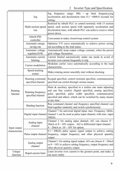
Jog Jog frequency range: 0Hz ~ up limit frequency;jog acceleration and deceleration time 0.1~6000.0 seconds for setting.
Multi-section speed run
Realized by inbuilt PLC or control terminal; with 15 section speed, each section speed with separately acceleration and deceleration time; with inbuilt PLC can achieve reserve when power down.
Inbuilt PID controller
Convenient to make closed-loop control system
Automatic energy saving run
Optimize V/F curve automatically to achieve power saving run according to the load status.
Automatic voltage regulate(AVR)
Automatically keep output voltage constant, when the power grid voltage fluctuation
Automatic current limiting
Current limited automatically under run mode in avoid of inverter over-current frequently to trip.
Carrier modulation Modulate carrier wave automatically according to the load characteristic.
Speed tracking restart
Make rotating motor smoothly start without shocking
Running function
Running command specified channel
Keypad specified, control terminal specified, communication specified can switch through various means.
Running frequency specified channel
Main & auxiliary specified to a realize one main adjusting and one fine control. Digital specified, analog specified, pulse specified, pulse width specified, communication specified and others, which can be switched by many means at any time.
Binding function Run command channel and frequency specified channel can bind together randomly and switch synchronously
Input output characteristic
Digital input channel Channel 7 for universal digital input, max. Frequency 1KHz, channel 1 can be used as pulse input channel, with max. input 50KHz.
Analog input channel
Channel 2 for analog input channel, AI1 can choose 4~20mA or 0~10V output,AI2 is differential input channel,4~20mA or -10~10V for option.
Pulse output channel 0.1~20KHz pulse square signal output to achieve setting frequency, output frequency and other physical quantity output.
Analog output channel
Channel 1 for analog signal output, AO can choose 4~20mA or 0~10V to achieve setting frequency, output frequency and other physical quantity output.
Unique function
Rapid current limit Limit inverter over current to the greatest point, and make it run more stably
2 Inverter Type and Specification
10
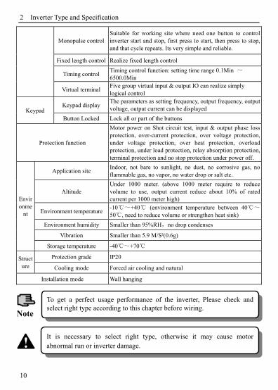
Monopulse control Suitable for working site where need one button to control inverter start and stop, first press to start, then press to stop, and that cycle repeats. Its very simple and reliable.
Fixed length control Realize fixed length control
Timing control Timing control function: setting time range 0.1Min ~ 6500.0Min
Virtual terminal Five group virtual input & output IO can realize simply logical control
Keypad Keypad display
The parameters as setting frequency, output frequency, output voltage, output current can be displayed
Button Locked Lock all or part of the buttons
Protection function
Motor power on Shot circuit test, input & output phase loss protection, over-current protection, over voltage protection, under voltage protection, over heat protection, overload protection, under load protection, relay absorption protection, terminal protection and no stop protection under power off.
Environme
nt
Application site Indoor, not bare to sunlight, no dust, no corrosive gas, no flammable gas, no vapor, no water drop or salt etc.
Altitude Under 1000 meter. (above 1000 meter require to reduce volume to use, output current reduce about 10% of rated current per 1000 meter high)
Environment temperature -10~+40 (environment temperature between 40~50, need to reduce volume or strengthen heat sink)
Environment humidity Smaller than 95%RH,no drop condenses
Vibration Smaller than 5.9 M/S²(0.6g)
Storage temperature -40~+70
Structure
Protection grade IP20
Cooling mode Forced air cooling and natural
Installation mode Wall hanging
To get a perfect usage performance of the inverter, Please check and select right type according to this chapter before wiring.
Note
It is necessary to select right type, otherwise it may cause motor abnormal run or inverter damage. !

3 Installation and wiring
11
3 Installation and wiring
3.1 Installation ambient
3.1.1 The demands for installation ambient (1) Installed in drafty indoor place,The ambient temperature should be within
-10ºC~40ºC,It needs external compulsory heat sink or reduce the volume if temperature is over than 40ºC.
(2) Avoid installing in places with direct sunlight, much dust, floating fiber and metal powder.
(3) Don’t install in place with corrosive, explosive gas. (4) The humidity should be smaller than 95%RH, Without condensation water. (5) Installed in place of plane fixing vibration smaller than 5.9m/s² (0.6g). (6) Keep away from electromagnetic disturbance source and other electronic
apparatus sensible to electromagnetic disturbance.
3.1.2 Installation direction and space (1) Normally the inverter should be mounted vertically, horizontal mounting
will seriously affect heat dissipation and the inverter must be used in lower volume. (2) Demand for minimum mounting space and distance, Please see Fig.3-1. (3) When installing multiple inverters up and down, leading divider must be
applied between them, See Fig. 3-2.
Fig.3-1 Mounting space Fig.3-2 Mounting of multiple inverters
导流隔板Leading divider 50mm
above
100mm above
100mm above
50mm
above
Exhaust
fan
3 Installation and wiring
12
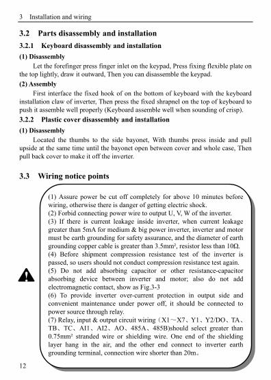
3.2 Parts disassembly and installation
3.2.1 Keyboard disassembly and installation
(1) Disassembly Let the forefinger press finger inlet on the keypad, Press fixing flexible plate on
the top lightly, draw it outward, Then you can disassemble the keypad.
(2) Assembly First interface the fixed hook of on the bottom of keyboard with the keyboard
installation claw of inverter, Then press the fixed shrapnel on the top of keyboard to push it assemble well properly (Keyboard assemble well when sounding of crisp). 3.2.2 Plastic cover disassembly and installation (1) Disassembly
Located the thumbs to the side bayonet, With thumbs press inside and pull upside at the same time until the bayonet open between cover and whole case, Then pull back cover to make it off the inverter.
3.3 Wiring notice points
(1) Assure power be cut off completely for above 10 minutes before wiring, otherwise there is danger of getting electric shock. (2) Forbid connecting power wire to output U, V, W of the inverter. (3) If there is current leakage inside inverter, when current leakage greater than 5mA for medium & big power inverter, inverter and motor must be earth grounding for safety assurance, and the diameter of earth grounding copper cable is greater than 3.5mm², resistor less than 10Ω. (4) Before shipment compression resistance test of the inverter is passed, so users should not conduct compression resistance test again.(5) Do not add absorbing capacitor or other resistance-capacitor absorbing device between inverter and motor; also do not add electromagnetic contact, show as Fig.3-3 (6) To provide inverter over-current protection in output side and convenient maintenance under power off, it should be connected to power source through relay. (7) Relay, input & output circuit wiring(X1~X7、Y1、Y2/DO、TA、TB、TC、AI1、AI2、AO、485A、485B)should select greater than 0.75mm² stranded wire or shielding wire. One end of the shielding layer hang in the air, and the other end connect to inverter earth grounding terminal, connection wire shorter than 20m。
!

3 Installation and wiring
13
Fig.3-3 Forbid to use contactor and absorbing capacitor
3.4 Main loop terminal wiring
Fig.3-4 Main loop simple wiring
UMEN630/
EN650A VW
L1(R)
L2(S)
L3(T)
Power source
Three phase circuit breaker
MEN630/ EN650A
U
V
W
(1) Before wiring, assure power supply is cut off completely for 10 minutes and all LED indicator light extinguished. (2) Wiring can only be done by professional person trained and qualified.(3) Before power on, check if voltage grade of the inverter is in line with that of power supply volt., otherwise will cause personnel injured and device damaged.
!

3 Installation and wiring
14
3.4.1 Connection between inverter and fitting parts (1) Breaking device like isolation Switch must assemble between power source and inverter to keep persona safety under repairing and inverter requirement for compulsory power off. (2) There must be over-current protection breaker or fuse in inverter power supply circuit to avoid failure expanding because of the second device failure. (3) AC input reactor When high harmonics between inverter and power supply is strong which cannot meet system requirement or input side power factor need to improve, ac input reactor can be added. (4) Contactor is used to power supply only, do not use it to control inverter start and stop. (5) Input side EMI filter Optionally EMI filter to restrain high frequency transduction interference and radio-frequency interference from inverter power line. (6) Output side EMI filter Choosing optionally EMI filter to restrain radio-frequency Interference and wire leakage current from inverter output side. (7) AC output reactor Installing AC output reactor is suggested to avoid motor insulation damage, oversize current leakage and inverter frequent protection when connecting wire between inverter and motor exceeds 50m. While to consider the voltage decrease issue of AC output rector, it can follow to boost inverter input & output voltage or use smaller power motor to avoid motor damage. (8) Safety earth ground wire Inverter and motor must be earth ground connection, connection wire should select as shorter and thicker as above 3.5mm² multi-core copper wire, and earth grounding resistance smaller than10Ω.
Fig.3-5 Connection of inverter and fitting parts
M
L1(R)
L2(S)
L3(T)N
Isolation switch
Breaker or fuse
Ac input reactor(In option)
Contactor
Input EMI filter(In option)
Brake unit(In option)
Input EMI filter(In option)
Ac output reactor(In option)
(+)(-)
U V W
L1 L2 L3(R)(S)(T)
EN630/EN650A

3 Installation and wiring
15
3.4.2 Main loop terminal wiring
Main loop input output terminal show as Table 3-1.
Table 3-1 Main loop input output terminal description
Adapted type Main loop terminal Terminal
name Function
description
EN630/EN650A-2S0004
~
EN630/EN650A-2S0015
L1 Zero line
L2 Live line
Grounding terminal
U、V、W 3phase AC output terminal
EN630/EN650A-4T0007
~
EN630/EN650A-4T0015
L1(R)、L2(S)、L3(T) 3phase AC input terminal
Grounding terminal
U、V、W 3phase AC output terminal
3.5 Basic running wiring diagram
Fig.3-6 Basic wiring diagram
U V WL1 L2
L1(R) U V WL2(S) L3(T)
L1(R)
L2(S)
L3(T)
+10V
X1
X2
X3
X4
X5
X6
X7
COM
Multifunction select 1
Multifunction select 2
Multifunction select 3
Multifunction select 4
Multifunction select 5
Multifunction select 6
Multifunction select 7
Note 1
+10V
AI2
AI1
GND
Internal optocoupleris olation input
(Multifunction selectcan use as high speedpulse input)
Speed command
-10~10V
0~10V or 4~20mA
U
V
W
M
GND
AO
Y2/DO
COM
Y1
+24V
2 circuit open collector output
Provide +24V power sourceoutside
TA
TB
TC
Fault relay output
485A
485B
Standard 485communication
P+ PB
Brake resistor (Extemal,fitting parts:connect to right side of inverter)
Power source
Note 2
H LSW1
EN630/EN650A
Analog meter4~20mA current signalor 0~10V voltage signal
Frequency meterOutput 24V pulse signal
Breaker

3 Installation and wiring
16
Note 1: When X1~X7 terminal input signal low electric level valid , push SW1 to “L” side. Note 2: When X1~X7 terminal input signal high electric level valid , push SW1 to “H” side.
3.6 Control loop collocation and wiring
3.6.1 Relative location and function for control board terminal and slide
switch: Control board terminal and slide switch location show as Fig.3-7. User terminal function explanation can be seen in Table 3-2, The setting
description and function of slide switch check Table3-3, Terminal CN3 is for manufacturer usage. Please do the right terminal wiring and setting to the switch on control board before using inverter and it is suggested to use greater than 24 AWG cable to connect terminal.
Fig 3-7 Sketch map of CPU board
3 Installation and wiring
17
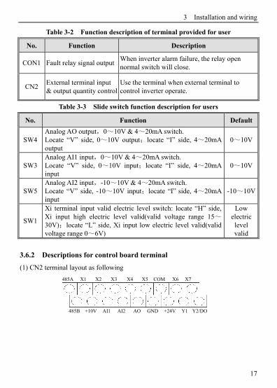
Table 3-2 Function description of terminal provided for user
No. Function Description
CON1 Fault relay signal output When inverter alarm failure, the relay open normal switch will close.
CN2 External terminal input & output quantity control
Use the terminal when external terminal to control inverter operate.
Table 3-3 Slide switch function description for users
No. Function Default
SW4 Analog AO output,0~10V & 4~20mA switch. Locate “V” side, 0~10V output;locate “I” side, 4~20mA output
0~10V
SW3 Analog AI1 input,0~10V & 4~20mA switch. Locate “V” side, 0~10V input;locate “I” side, 4~20mA input
0~10V
SW5 Analog AI2 input,-10~10V & 4~20mA switch. Locate “V” side, -10~10V input;locate “I” side, 4~20mA input
-10~10V
SW1
Xi terminal input valid electric level switch: locate “H” side, Xi input high electric level valid(valid voltage range 15~30V);locate “L” side, Xi input low electric level valid(valid voltage range 0~6V)
Low electric level valid
3.6.2 Descriptions for control board terminal
(1) CN2 terminal layout as following
+10V
X1 X2 X3 X4 X5 COM X6 X7 485A
AI1 AI2 GND AO Y2/DO +24V Y1 485B

3 Installation and wiring
18
(2) CN2 terminal function description show as Table 3-4
Table 3-4 Function table for control board terminal
Type Symbol Description Terminal Function Specification
Multfunction input terminal
X1 Multifunction input 1
Programmable defined as multifunction switch quantity input terminal, see switch quantity input function parameter (F08 group) input terminal description.
Input impedance: R=2KΩ Max. input frequency:200Hz X6、X7 can used as encoder input Max. input frequency:50KHz Input voltage range:15~30V
X2 Multifunction input 2
X3 Multifunction input 3
X4 Multifunction input 4
X5 Multifunction input 5
X6 Multifunction input 6
X7 Multifunction input 7/High-speed pulse input
+10V +10V power source Provide power source +10V outside(negative polarity:GND)
Max. output current:10mA
COM Common terminal +24V power negative polarity
+24V earth
GND +10V power negative polarity
Analog signal and +10V power source reference
Analog inpu
AI1 Analog input AI1
Accept analog Voltage/Current quantity input, voltage, current selected by switch SW3, factory default is voltage. (Reference: GND)
Input voltage range: 0~10V (Input impedance: 20KΩ) Input current range: 4~20mA (Input impedance: 250Ω) Resolution: 1/4000
AI2 Analog input AI2
Accept analog voltage quantity input,voltage, current selected by switch SW5.
Input voltage range: -10~10V (Input impedance: 20KΩ) resolution: 1/2000
Analog output
AO Analog output
Provide analog Voltage/Current quantity output, Output Voltage/ output current selected by switch SW4, Factory default is output voltage. (Reference: GND)
Current output range: 4~20mA Voltage output range: 0~10V

3 Installation and wiring
19
Multi- function output
terminal
+24V +24V power source Provide power source +24V outside(negative polarity: COM)
Max. output current:100mA
Y1 Open circuit collector output terminal 1
Programmable defined as multi-function pulse signal output terminal, particulars see switch quantity, analog quantity function parameter (F09 Group) terminal introduce
Max. output voltage:30V Max. output current:50mA
Y2/DO
Open circuit collector output terminal 2/ High speed pulse input terminal
Through F00.22 to select terminal output means as open collector output, with same specification as Y terminal, when used to high pulse output: output pulse voltage is 24V, output frequency max. is 20KHz.
(3) RS485 terminal function description show as Table 3-5
Table 3-5 RS485 terminal function on control board
Type Symbol Description Terminal Function Specification
Communication
485A 485 communication interface
485 differential signal positive terminal
Standard 485 communication port should use shielding wire or twisted wire.
(4) Terminal CON1, layout as following:
(5) CON1 terminal function description show as Table 3-6
Table 3-6 CON1 Terminal function on control board
Type Symbol Description Terminal Function Specification
Relay output
terminal
TA
Fault output relay
Normal: TB-TC close,TA-TC open Alarm: TB-TC open,TA-TC close
TB-TC: Close normal,TA-TC: Open normal. Contactor capacity: AC250V/2A (COSΦ=1) AC250V/1A (COSΦ=0.4)DC30V/1A
TB
TC
TA TB TC

3 Installation and wiring
20
3.6.3 Analog input & output terminal wiring
(1) AI1 receive analog voltage signal input, Wire as below:
Fig.3-8 AI1 Terminal wiring diagram
(2) AI2 receive analog signal input, input voltage (-10~10V) and input current (4~20Ma), wire as below:
Fig.3-9 AI2 Terminal wiring diagram
(3) Analog output terminal AO wire Analog output terminal AO external connect to analog meter can indicate several physical quantity, wire as below:
Fig.3-10 AO Terminal wiring diagram
+
―
AI1
Shield cable near-end earth grounding
0~+10V or4~20mA
EN630/ EN650A
+10V
GND
+
―
+10V
Shield cable near-end earth grounding
-10~+10V
or 4~20mA
EN630/ EN650A
AI2
GND
Analog meter
AO
GND
EN630/ EN650A

3 Installation and wiring
21
3.6.4 Communication terminal wiring
EN630/EN650A inverter provide RS485 serial communication interface to user. The following wire connection can make up of single-main single-sub control
system or single-main multi-sub control system. To use host computer software(PC or PLC controller)can realize real time monitoring and operation to inverter,and to achieve complicated run control like long-distance control, high degree automation. It can also use one host inverter and others slave inverter to make up of the cascade or synchronous control inverter network.
(1) Inverter RS485 interface and other device with RS485 interface wire connection how as following
Fig.3-11 Communication terminal wiring (2) Inverter RS485 interface and host computer (Device with RS232 interface)
connection:
Fig.3-12 RS485 communication wiring
EN630
/EN650A
RS485
A(485+)
B(485-)
A(485+)
B(485-)
Device with
RS485 or
EN630
/EN650A
Name Description
B +5V
TXD
A RXD
GND
RS232/RS485 converter
Description Name
Signal terminal B
Signal A
EN630/EN650A inverter Host computer
Sign Pin No.
shell
RXD 2
TXD 3
GND 5
DTR 4
DSR 6
RI 9
CD 1
RTS 7
CTS 8
Shield cable
(1) Under analog input mode, filter capacitor or common mode choke can be installed between AI1 and GND or AI2 and GND. (2) Analog input and output signal can be interfered easily by ambient environment, it need use shield cable for connection andearth grounding well as short as possible.Note
3 Installation and wiring
22
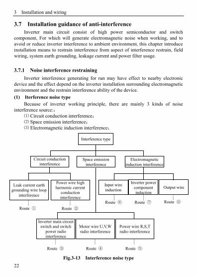
3.7 Installation guidance of anti-interference Inverter main circuit consist of high power semiconductor and switch
component, For which will generate electromagnetic noise when working, and to avoid or reduce inverter interference to ambient environment, this chapter introduce installation means to restrain interference from aspect of interference restrain, field wiring, system earth grounding, leakage current and power filter usage.
3.7.1 Noise interference restraining
Inverter interference generating for run may have effect to nearby electronic device and the effect depend on the inverter installation surrounding electromagnetic environment and the restrain interference ability of the device.
(1) Iterference noise type Because of inverter working principle, there are mainly 3 kinds of noise
interference source:: ⑴ Circuit conduction interference; ⑵ Space emission interference; ⑶ Electromagnetic induction interference;
Fig.3-13 Interference noise type
Inverter main circuit switch and switch
power radio interference
Motor wire U,V,W radio interference
Power wire R,S,T radio interference
Route ③ Route ④ Route ⑤
Space emission interference
Interference type
Leak current earth grounding wire loop
interference
Power wire high harmonic current
conduction interference
Circuit conduction interference
Route ① Route ②
Electromagnetic induction interference
Input wire induction
Inverter power component induction
Output wire
Route ⑥ Route ⑦ Route ⑧

3 Installation and wiring
23
(2)Noise transmission route
Fig.3-14 Noise interference transmission route diagram
(3)Basic countermeasure for restrain interference
Table 3-7 Interference restrain countermeasure
Noise spread road
Countermeasure of weakening effect
①
Earth grounding cable of peripheral device and inverter wiring make up of the closed-loop and leakage current of inverter earth grounding cable will make device perform wrong action. It will decrease wrong action when device not connect to earth grounding.
②
When the power of peripheral device and inverter power belong to the same power source, high harmonic generating from inverter will transmit the voltage and current along with the power line which will interfere other devices within the same power source system. Take some restraining measures as below:install electromagnetic noise filter at inverter input end; use isolation transformer to isolate other devices; connect power end of peripheral device to remote power grid;add power ferrite filter magnetic ring to inverter R、S、T three phase wire to restrain high harmonic current conduction
③④⑤
Keep other sensitive devices and signal wire installed away from inverter. it should use shield wire and make the shield layer single end earth grounding. Besides keep distance from inverter and its input & output wire as possible as. When signal wire need to intersect with strong current cable, it should make them orthogonal crossing not parallel. Install high frequency noise filter (ferrite common code choke, also called magnetic ring) at the bottom end of the inverter input & output to restrain radio
Sensor power inverter Wireless device meter
motor sensor
TV
①
⑦
⑧
⑥ ⑤
②
⑤

3 Installation and wiring
24
frequency interference of dynamic wire effectively. Motor cable should be placed in protective object with large thickness, such as placed in larger thickness(over 2mm) pipeline or buried in cemented tank. Putting dynamic wire in metal tube and connect to earth grounding with shield wire (motor cable use 4-core cable, one side is earthed through the inverter, the other side connected to motor casing).
⑥⑦⑧
To prevent wire parallel or bundled of strong and weak current, it should keep away from inverter assemble device, and wiring should away from inverter R,S,T,U,V,W power line. Devices with high field and high magnetic field should notice the corresponding installation position of inverter and keep distance and orthogonal crossing.
3.7.2 Field wiring and earth grounding
(1) Inverter terminal motor connection wire (U,V,W terminal output wire) and inverter terminal power connection wire (R,S,T terminal input wire) should keep distance enough as more as 30cm.
(2) U,V,W terminal 3 motor wires should be placed in metal tube or metal wiring tank as possible as.
(3) Generally control signal wire should use shield cable, when shield layer connect to inverter terminal, it should be the single end earth grounding which closed to inverter side.
(4) Inverter terminal earth grounding cable must directly connect to floor, it cannot connect to earth grounding through other device.
(5) Strong current cable(R,S,T,U,V,W) cannot parallel wiring closely with control signal wire, and bundled together is prohibited. It should keep distance from over 20~60 cm (relative to strong current size). When it’s necessary to intersect, it should be orthogonal crossing, show as Fig.3-15.
Fig.3-15 System wiring demand (6) Earth grounding wire for strong current should separately connect to earth
grounding with control signal and sensor earth grounding wire for weak current. (7) Forbid to connect inverter input terminal (R,S,T) to other devices.
电源线或电动机线
控制信号线
Power wire or motor cable
Control signal wire

3 Installation and wiring
25
3.7.3 Long distance wiring & Leak current and countermeasure
When inverter connect to motor in a long distance, High harmonic wave through distributed capacitance will generate leak current to earth and wire-to-wire. Restraining methods as below:
(1) Install ferrite magnetic ring or output reactor at the inverter output terminal.
(2) As carrier frequency low, the motor noise would increase accordingly.
3.7.4 Installation demand for electromagnetic on-off electronic device
It should pay attention that surge absorber must be installed when electromagnetic on-off electronic device like relay, electromagnetic contactor and electromagnetic iron generating noise easily and largely installed near to inverter or in the same control cabinet, show as Fig.3-16.
Fig.3-16 Install demand for electromagnetic on-off device
变频器或其
它电气设备
压敏电阻器
二极管
RC-滤波器
220VAC
220VAC
24VDC
+
_
~
~
~
~
Diode
filter
Varistor
Inverter or other devices
When reactor installed with rated voltage drop more 5% and long wiring to U, V, W terminal, It would reduce motor’s voltage apparently. When motor run at full load, It is possible to flash motor, and it should be used by derating or boosting input and output voltage.
!

4 Run and operation explanation for inverter
26
4 Run and operation explanation for inverter
4.1 Run of inverter
4.1.1 Running order channels There are 3 kinds of order channel for controlling run action of the inverter such
as run, stop, jog etc. 0:Keypad Control by key 、 、 on keypad (Factory default). 1:Control terminal Use control terminal Xi (Defined as FWD), Xi (Defined as REV) and COM to
make of double-line control, or use anyone terminal of X1~X8 except terminal FWD and REV to make of three-line control.
2:Communication port Control run and stop of the inverter through upper machine or other device which
can communicate with the inverter. Choose order channel by setting function code F01.15;and also can choose by
multi-function input terminal (F08.18~F08.25 choose function 49,50,51,52,53).
4.1.2 Frequency-provision channel EN630/EN650A includes main frequency provision and assist frequency
provision: Main frequency provision: 0: Keypad analog potentiometer provision; 1: AI1 analog setting; 2: AI2 analog setting; 3: Terminal UP/DOWN adjustment provision; 4: Communication provision (Communication address: 1E01); 5: Reserved; 6: Reserved; 7: High speed pulse provision (X7 terminal need select the corresponding
function); 8~14: Reserved Assist frequency provision:
Please make switching debugging in advance when switch the order channel to check if it can fulfill system requirement, otherwise have danger of damaging device and injuring personal.
!

4 Run and operation explanation for inverter
27
0: Keypad analog potentiometer provision; 1: AI1 analog setting; 2: AI2 analog setting; 3: Terminal UP/DOWN adjustment provision; 4: Communication provision (Communication address: 1E01); 5: Reserved; 6: Reserved; 7:Terminal pulse provision (X7 terminal need select the corresponding function); 8~20: Reserved
4.1.3 Work state Work state of EN630/EN650A includes of Waiting state, Running state and
Parameter setting state. Waiting state : If there is no running command after the inverter electrified or after stop
command during running state, the inverter enters into waiting state. Running state: The inverter enters into running state after receiving run command. Parameter setting state: After receiving the parameter identification command, enter the parameter
setting state, then turning into the shutdown state.
4.1.4 Run mode EN630/EN650A inverter have 6 kinds of run mode, following is in turn
according to their priority, Jog run→Closed-loop run→PLC run→Multi-section speed run→Swing frequency run →Common run. Shown as Fig.4-1.

4 Run and operation explanation for inverter
28
Fig.4-1 Logic flow chart of EN630/EN650A inverter running state
N
High priority
Low priority
Electrification
Any jog command?
N
Waiting state
Closed-loop effective?
Y
N
PLC effective?
Traverse run?
Common run?
Multi-section terminal effective?
N
N
N
N
Run command effective?
Y
Y
Jog run
Closed-loopRun
PLC Run
Multi-section Run
Traverse run
Common run
Y
Y
Y
Y
Y
Y
Closed-loop invalidation terminal closed?
PLC invalidation Terminal closed?
N
N

4 Run and operation explanation for inverter
29
0:Jog run Upon receiving jog run command (For instance, press the key on keypad)
during waiting state, the inverter run at jog frequency (see function code F01.25~F01.29).
1:Closed-loop run The inverter will come into closed-loop run mode when closed –loop run control
effective parameter is set (F11.00=1 or F12.00=5). Namely carry on PID adjustment to specified value and feedback value (Proportion integral differential calculation, see F11 Group function code) and PID adjuster output is inverter output frequency. Can make closed-loop run mode ineffective and switch to lower level run mode by multi-function terminal (Function 31).
2:PLC run The inverter will enter into PLC run mode and run according to run mode preset
(See F10 Group function code description) through setting PLC function effective parameter(F10.00 last bit≠0). Can make PLC run mode ineffective and switch to lower level run mode by multi-function terminal (function 36).
3:Multi-section speed run By nonzero combination of Multi-function terminal (5, 6, 7, 8, function), choose
multi-section frequency 1~15(F10.31~F10.45) to run at multi-section speed.
4:Swing frequency run The inverter will enter into swing frequency run mode when swing frequency
function effective parameter (F13.00=1) is set. Set relevant swing frequency run special parameter according to textile swing frequency craft to realize swing frequency run.
5:Common run Common open loop run mode of general inverter. In above 6 kinds of run mode except “jog run” the inverter can run according to
kinds of frequency setting method.
4.2 Operation and use of key board
4.2.1 Keypad layout The operating keyboard is the main unit of frequency inverter to accept
commands, display parameters. Keyboard outline diagram shown in Fig.4-2.

4 Run and operation explanation for inverter
30
Fig.4-2 Keypad layout sketch
4.2.2 Keypad function description There are 8 Key-presses and a digital potentiometer on inverter keypad,and
function definition of each key is as shown in Table 4-1.
Table 4-1 Keypad function table
Key Name Function description
Program/Exit key Enter into or exit programming state
Shift/Supervision
key
Can choose modification digit of set data under editor state;
can switch display status supervision parameter under other state
Function/Data key Enter into or exit programming state
Rev/Jog key
Under keypad mode: to press this key can set reverse run or Jog
run according to the 1st bit of parameter F00.15
Run key Enter into forward run under keypad mode
Stop/reset key
In common run status the inverter will be stopped according to
set mode after pressing this key if run command channel is set as
keypad stop effective mode. The inverter will be reset and
resume normal stop status after pressing this key when the
inverter is in malfunction status.
Failure alarm indicator light Forward run indicator light
Reverse run indicator light
Mode indicator light
Digital display(LED)
UP
Program/exit key
shift/supervision key
Rev/jog key
Current unit(A)
Frequency unit(Hz)
Voltage unit(V)
Digital potentiometer
Confirm/Date keyDecrease keyStop/reset keyForward run key

4 Run and operation explanation for inverter
31
Digital
potentiometer
It is the same as the function of increase and decrease key,
rotate to the left means decrease, rotate to the right means
increase.
Increasing button
To increase data or function code (to press it continuously can
improve increasing speed)
Decreasing button
To decrease data or function code (to press it continuously can
improve decreasing speed)
4.2.3 LED and indicator light
4 status indicator light: They are MOD(mode):ALM(alarm):FWD(forward run): REV(reverse run)from left to right on the LED: Their respective indicating meaning is as shown in Table 4-2.
Table 4-2 Status indicator light description
4.2.4 Key board display status
EN630/EN650A keypad display status is classified as Waiting status parameter display; Function code parameter editing status display; Malfunction alarm status display; Run status parameter display; Alarm state display in total 5 kinds of status. LED indicator light will all be lit after the inverter electrified. Then enter into set
Item Function description
Display
function
Digital display Display current run status parameter and set parameter
Status
indicato
r light
A、
Hz、V
Unit for relevant current digital displayed physical
parameter(Forcurrent is A:for voltage is V:for frequency is Hz)
MOD
This indicator light is lit in non-supervision status and
extinguished if no key pressed for a minute: then come back to
supervision status
ALM
Alarm indicator light: indicate that the inverter is in over current
or over voltage suppressing status or failure alarm status
currently
FWD
Forward run indicator light, indicate
that the inverter output forward phase
order and the connected motor rotate in
forward direction
The inverter work in
DC brake status if
FWD,REV indicator
light is lit at the same
time REV
Reverse run indicator light: indicate
that the inverter output reverse phase
order and the connected motor rotate in
reverse direction

4 Run and operation explanation for inverter
32
frequency display. As shown in Fig.4-3 a.
(1) Waiting parameter display status The inverter is in waiting status and waiting status supervision parameter is
displayed on keyboard: normally parameter F00.13 decide which status supervision parameter to be displayed. As shown in Fig.4-3 b, the indicator light shows the unit of the parameter.
To press key, It can display different waiting status supervision parameter circularly: For detail please see C-00 to C-05 group supervision parameter details decide by F00.07~F00.12.
(2) Run parameter display status The inverter enters into run status when receiving effective run command and
normally parameter F00.13 decide which status supervision parameter to be displayed on the keypad. As shown in Fig.4-3 c, The indicator light shows the unit of the parameter.
To press key can display run status supervision parameter circularly. For detail please see C-00 To C-05 group supervision parameter details decide by F00.01~F00.06 .
Fig.4-3 Inverter electrification: waiting: run status display
Fig.a Electrification, display 8.8.8.8.8.
Fig.b Waiting status, display waiting status parameter
Fig.c Run status: display Run status parameter
Set frequency Out frequency

4 Run and operation explanation for inverter
33
(3) Failure alarm display status
The inverter enters into failure alarm display status upon detecting failure signal and display failure code sparklingly(as shown in Fig.4-4);To press key can look over relative parameter after stopping running;Can press key to enter into program status to see about F26 group parameter if want to search failure information.Can carry on failure restoration by
key: Control terminal or communication command on the keypad after troubleshooting. Keep displaying failure code if failure exist continuously.
(4) Function code editing status
Under waiting, run or failure alarm status, press key, can enter into editing status(If user password is set, can enter into editing status after inputting the password, see also F27.00 description and Fig.4-10),and editing status is displayed according to three classes menu mode, as shown in Fig. 4-5. To press key can enter into one class by one class. Under function parameter display status, press key to carry on parameter storage operation; press key can only come back to upper class menu without storing modified parameter.
Fig.4-5 Keypad display status switching
Fig.4-4
over current in
Para.group Display controlOutput frequency
Switch display
ESC/MENUESC/MENU
ESC/MENU First class menu ENTER/DATA Second-class menu
Electrification
Waiting status parameter Displayor run status parameter displayor failure alarm display
For some serious failure, such as inverse module protect, over current: over voltage etc. must not carry on failure reset forcibly to make the inverter run again without failure elimination confirmed. Otherwise have danger of damaging the inverter!
!

4 Run and operation explanation for inverter
34
(5) Alarm state display
When under running and standby situation: It means enter failure alarm display status upon detecting failure signal and display failure code sparklingly(Fig.4-6)Inverter keeping running state But this alarm display can not be reset button eliminated: After only find the cause of the alarm: in order to eliminate this factor Normal.
4.2.5 User Management Parameters In order to facilitate the user parameter management: EN630/EN650A
component model parameter menu for display management. The parameters do not need to be displayed can be shielded.
(1) Method parameter setting mode display. By setting F00.00 = 0,1,2,3 respectively parameter mode is set: Basic menu
mode: menu mode Intermediate: Advanced menu mode and user menu mode. Basic menu F00,F01,F02,F03,F26
Middle
menu
F00,F01,F02,F03,F04,F05,F06,F07,F08,F09,F10,F11,F12,F13,F14,
F15,F16,F18,F19,F26
Advance
menu
F00,F01,F02,F03,F04,F05,F06,F07,F08,F09,F10,F11,F12,F13,F14,
F15,F16,F17,F18,F19,F20,F21,F22,F23,F24,F25,F26,F27
User
custom F00.00 and F25 parameters group
4.2.6 Method for operating keypad
Can carry on various operation to the inverter through keypad, for example:
(1) Status parameter display switching: After pressing key , Display C group status supervision parameter; after
displaying one supervision parameter code for 1 second will display this parameter value automatically. Press key will go back to supervision interface.
Fig.4-6
Same main/assist frequency
channel

4 Run and operation explanation for inverter
35
Fig.4-7 Waiting status parameter display operating example
(2) Function code parameter setting Take function code F01.01 modified from 5.00Hz to 6.00Hz as
example.Boldface in Fig.4-8 shows flickering digit.
Fig.4-8 Example for parameter setting and modification
Description: under second -class menu: if the parameter has no blinking digit, this function code can’t be modified, possible reasons are as follows:
1>This function code shouldn’t be modified: for example actual detected status parameter: run record parameter etc.;
2>This function code can’t be modified under run status and can be changed after stopping running;
3>Parameter protected. All the function code can’t be modified when function code F00.14=1 or 2, In order to avoid wrong operation. Need to set the function code F00.14 to 0 if you want to edit function code parameter.
C-00
∫…∫
Para. C-051s
Para. C-031s
Key-press operationorder
0.00 C-01 Para.1s
C-02 Para.1sLED displayed
content
…
0.00 F00.00 F01.00 F01.00 F01.01
Exit editingstantus
Enter intoediting Statusdisplay first-classmenu
Choose F01group functioncode
Move to theposition to beadjusted
Choosefunction codeF01.01
LED displayedcontent
Key-pressoperationorder
Store modifiedvalue:back tofirst-class menuDisplay nextfunction code
Parametermodification,5→6
Parametermodification,Choose parameterdigit
Function codeconfirmation,Enterintosecond-class
F01.02 006.00 005.00 005.00

4 Run and operation explanation for inverter
36
(3) Specified frequency adjustment for common run Take example modifying specified frequency from 50.00Hz to 40.00Hz at
F01.06=1, F01.03=0 during running for explanation.
Fig.4-9 Set frequency adjustment operation example
(4) Jog run operation For example: keypad as current run command channel: jog run frequency 5Hz:
waiting status.
Fig.4-10 Jog run operating example
(5) Operation for entering to function code editing status after setting user
password For example: “User password” F27.00 is set to“12345”. Boldfaced digit in
Fig.4-11 shows blinking bit.
50.00 49.99
Press decreasingbutton for onetime
Adjust frequencybased onrequirement
45.00LED displayedcontent
Key-pressoperation order
…
40.00
Stop pressing after setvalue reached:go backto nomal display statusafter 1s
0.00 0.01
Displayset frequency
5.00LED displayedcontent
Key-pressoperation order
…
0.01 0.00
WaitingWaiting
PressKeep
Release
Displayoutput frequency
Output frequencyIncreased by 5Hz
Output frequencyFall down to 0HzStop running

4 Run and operation explanation for inverter
37
Fig.4-11 Inputting password to go into function code operation
(6) See about failure parameter under failure status: If press key under failure status the user can quickly locate to the F26 group
function code parameter. Press can quickly switch value between F26.04 ~ F26.10 parameters and fault alarm, easy to view the fault records.
(7) Keypad key-press locking operation
Under unlocked keypad situation , press key for 2s to lock the keypad. For detailed operation please refer to 2nd bit of F00.14 function code.
(8) Keypad key-press unlocking operation
Under locked keypad situation, press key for 5s to unlock the keypad.
4.3 Inverter electrification
4.3.1 Check before electrification Please carry on wiring based on operation requirement provided in “inverter
wiring” of this Service manual.
4.3.2 First electrification Close input side AC power supply switch after correct wiring and power supply
0.00 00000
None-editingstatus
10000LED displayedcontent
Key-pressoperation order
10000 12000
User passwordeffective:go intopassword validationstatus
At first lastDigit flash,Increase to"1"
Move cursorposition toforth digit
F27.00
12345
Increaseto "2"
1234012340 12300 12300 12000
Move tothe unit
Increase to "4" Move tosecond
Increaseto "3"
Move to third
Increase to "5" Press confirmationKey:pass validation,Go into editing status
4 Run and operation explanation for inverter
38
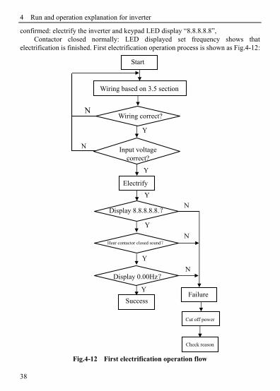
confirmed: electrify the inverter and keypad LED display “8.8.8.8.8”, Contactor closed normally: LED displayed set frequency shows that
electrification is finished. First electrification operation process is shown as Fig.4-12:
Fig.4-12 First electrification operation flow
Start
Wiring based on 3.5 section
Wiring correct?
Input voltage correct?
Display 8.8.8.8.8.?
Hear contactor closed sound?
Display 0.00Hz?
Electrify
Cut off power
Success
Check reason
Failure
Y
Y
Y
Y
Y
Y
N
N
N
N
N
5 Function parameter schedule graph
39
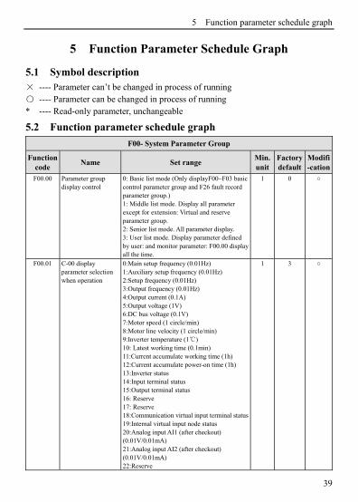
5 Function Parameter Schedule Graph
5.1 Symbol description × ---- Parameter can’t be changed in process of running ---- Parameter can be changed in process of running * ---- Read-only parameter, unchangeable
5.2 Function parameter schedule graph
F00- System Parameter Group
Function code
Name Set range Min. unit
Factory default
Modifi-cation
F00.00 Parameter group display control
0: Basic list mode (Only displayF00~F03 basic control parameter group and F26 fault record parameter group.) 1: Middle list mode. Display all parameter except for extension: Virtual and reserve parameter group. 2: Senior list mode. All parameter display. 3: User list mode. Display parameter defined by user: and monitor parameter: F00.00 display all the time.
1 0
F00.01 C-00 display parameter selection when operation
0:Main setup frequency (0.01Hz) 1:Auxiliary setup frequency (0.01Hz) 2:Setup frequency (0.01Hz) 3:Output frequency (0.01Hz) 4:Output current (0.1A) 5:Output voltage (1V) 6:DC bus voltage (0.1V) 7:Motor speed (1 circle/min) 8:Motor line velocity (1 circle/min) 9:Inverter temperature (1 ) 10: Latest working time (0.1min) 11:Current accumulate working time (1h) 12:Current accumulate power-on time (1h) 13:Inverter status 14:Input terminal status 15:Output terminal status 16: Reserve 17: Reserve 18:Communication virtual input terminal status19:Internal virtual input node status 20:Analog input AI1 (after checkout) (0.01V/0.01mA) 21:Analog input AI2 (after checkout) (0.01V/0.01mA) 22:Reserve
1 3

5 Function parameter schedule graph
40
23:Reserve 24:Analog AO output (after checkout) (0.01V /0.01mA) 25:Reserve 26:Reserve 27:Reserve 28:External pulse input frequency (Before checkout) (1Hz) 29:Reserve 30:Process PID provide (0.01V) 31:Process PID feedback (0.01V) 32:Process PID deviation (0.01V) 33:Process PID output (0.01Hz) 34: Simple PLC current segment No. 35: External multi-speed current segment No. 36:Constant pressure water supply provide pressure (0.001Mpa) 37:Constant pressure water supply feedback pressure (0.001Mpa) 38:Constant pressure water supply relay status39:Current length (1M) 40:Accumulate length (1M) 41:Current internal count value 42:Current internal time value 43:Run command setup channel (0:Keyboard 1:Terminal 2:Communication)44:Main frequency provide channel 45:Auxiliary frequency provide channel 46:Rated current (0.1A) 47:Rated voltage (1V) 48:Rated power (0.1KW) 49:Electric torque limit value (0.1% motor specified torque) 50:Braking torque limit value (0.1% motor specified torque) 51:Frequency after add or subtract speed (0.01Hz) 52:Motor rotor frequency (0.01Hz) 53:Current present torque (Relate specified percent of torque, with direction) 54:Current output torque (Relate specified percent of torque, with direction) 55:Torque current at present (0.1A) 56:Flux current at present (0.1A) 57:Setting motor speed (r/min) 58:Output power (Act power) (0.1kw) 59:Total electric cost low-order (1 degree) 60:Total electric cost high-order (1 means 10,000degree) 61-65:Reserve
F00.02 C-01 display parameter selection
Same as above 1 2
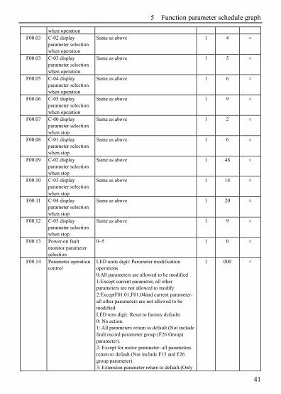
5 Function parameter schedule graph
41
when operation F00.03 C-02 display
parameter selection when operation
Same as above 1 4
F00.03 C-03 display parameter selection when operation
Same as above 1 5
F00.05 C-04 display parameter selection when operation
Same as above 1 6
F00.06 C-05 display parameter selection when operation
Same as above 1 9
F00.07 C-00 display parameter selection when stop
Same as above 1 2
F00.08 C-01 display parameter selection when stop
Same as above 1 6
F00.09 C-02 display parameter selection when stop
Same as above 1 48
F00.10 C-03 display parameter selection when stop
Same as above 1 14
F00.11 C-04 display parameter selection when stop
Same as above 1 20
F00.12 C-05 display parameter selection when stop
Same as above 1 9
F00.13 Power-on fault monitor parameter selection
0~5 1 0
F00.14 Parameter operation control
LED units digit: Parameter modification operations 0:All parameters are allowed to be modified 1:Except current parameter, all other parameters are not allowed to modify 2:ExceptF01.01,F01.04and current parameter,all other parameters are not allowed to be modified LED tens digit: Reset to factory defaults 0: No action. 1: All parameters return to default.(Not include fault record parameter group (F26 Group) parameter). 2: Except for motor parameter: all parameters return to default.(Not include F15 and F26 group parameter). 3: Extension parameter return to default.(Only
1 000 ×

5 Function parameter schedule graph
42
F21~F24 group parameter return to default). 4: Virtual parameter return to default.(Only F20 group parameter return to default). 5:Fault record return to default.(Only fault record parameter group (F26 Group) parameter return to default) LED hundreds digit: key operation 0:All locked 1:Except button: the others locked 2:Except , , button: the others locked 3:Except , button: the others locked.4:Except , button: the others locked.
F00.15 Button function selection
LED units digit: panel button selection 0:Reversal command action button 1:Jog action button LED tens digit: Reserve LED hundreds digit: terminal run command control 0:Keyboard button invalid 1:Keyboard button valid LED thousands digit: communication run command control 0:Keyboard button invalid 1:Keyboard button valid
1 0001
F00.16 Multi-function key run command channel switching order selection
0: Keyboard control→ Terminal control→ Communication control 1: Keyboard control←→ Terminal control 2: Keyboard control←→ Communication control 3: Terminal control←→communication control
1 0
F00.17 Motor speed display coefficient
0.1~999.9% 0.1% 100.0%
F00.18 Line speed display coefficient
0.1~999.9% 0.1% 1.0%
F00.19 PG card valid selection
0:Invalid 1:Reserve 2:Reserve 3:Incremental PG coder card(F08.24 can’t be 91) (Terminal X6, X7 correspond A, B; terminal X5 correspond Z) 4~10:Reserved
1 0 ×
F00.20 Analog input terminal configuration
LED Units digit:AI1 configuration 0:0~10V input 1:4~20mA input LED tens digit: AI2 configuration 0:-10~10V input 1:4~20mA input LED Hundreds digit: Reserve LED Thousands digit: Reserve
1 0000 ×
F00.21 Analog output terminal
LED units digit: AO configuration 0:0~10V output
1 0000 ×
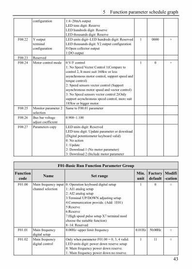
5 Function parameter schedule graph
43
configuration 1:4~20mA output LED tens digit: Reserve LED hundreds digit: Reserve LED thousands digit: Reserve
F00.22 Y output terminal configuration
LED units digit~LED hundreds digit: ReservedLED thousands digit: Y2 output configuration0:Open collector output 1:DO output
1 0000 ×
F00.23 Reserved F00.24 Motor control mode 0:V/F control
1: No Speed Vector Control 1(Compare to control 2, It more suit 160kw or less asynchronous motor control, support speed and torque control) 2: Speed sensors vector control (Support asynchronous motor speed and vector control)3: No Speed sensors vector control 2(Only support asynchronous speed control, more suit 185kw or bigger motor.
1 0 ×
F00.25 Monitor parameter 2 selection
Same to F00.01 parameter
F00.26 Bus bar voltage adjust coefficient
0.900~1.100
F00.27 Parameters copy LED units digit: Reserved LED tens digit: Update parameter or download (Digital potentiometer keyboard valid) 0: No action 1: Update 2: Download 1 (No motor parameter) 3: Download 2 (Include motor parameter
F01-Basic Run Function Parameter Group
Function code
Name Set range Min. unit
Factory default
Modifi-cation
F01.00 Main frequency input channel selection
0: Operation keyboard digital setup 1: AI1 analog setup 2: AI2 analog setup 3:Terminal UP/DOWN adjusting setup 4:Communication provide. (Add: 1E01) 5:Reserve 6:Reserve 7:High speed pulse setup X7 terminal need choose the suitable function) 8~14: Reserved
1 0
F01.01 Main frequency digital setup
0.00Hz~upper limit frequency 0.01Hz 50.00Hz
F01.02 Main frequency digital control
Only when parameter F01.00 = 0, 3, 4 valid. LED units digit: power down reserve setup 0: Main frequency power down reserve. 1: Main frequency power down no reserve.
1 11

5 Function parameter schedule graph
44
LED tens digit: halt reserve setup 0:Halt main frequency hold 1:Halt main frequency recovery F01.01 LED hundreds digit: Communication provide frequency data setup 0:Definit frequency setup (Provide 5,000 means 50.00 Hz) 1:Provide 10,000 means upper limit frequency (F01.11)
F01.03 Auxiliary frequency input channel select
0: Operation keyboard digital setup 1: AI1 analog setup 2: AI2 analog setup 3: Terminal UP/DOWN adjusting setup 4: Communication provide. 5: Reserve. 6: Reserve 7: Terminal pulse setup (X7 terminal need choose the suitable function) 8~10: Reserved 11: Process PID provide 12~20: Reserved
1 1
F01.04 Auxiliary frequency digital setup
0.00Hz~Upper limit frequency 0.01Hz 0.00Hz
F01.05 Auxiliary frequency digital
LED units digit: Power down reserve setup 0: Auxiliary frequency power down reserve. 1: Auxiliary frequency power down no reserve. LED tens digit: Halt reserve setup 0: Halt auxiliary frequency hold. 1: Halt auxiliary frequency recovery parameter F01.04
1 11
F01.06 Main and auxiliary provide calculating setup
0: Main frequency (Complex frequency of current is main frequency). 1: Auxiliary frequency (Complex frequency of current is auxiliary frequency.) 2: Plus (Polarity oppose of complex and main frequency, Complex frequency is zero). 3: Minus (Polarity oppose of complex and auxiliary frequency, Complex frequency is zero). 4: Multiplication (Polarity opposed of main and auxiliary frequency: Complex frequency is zero). 5: Max(The max frequency of main and auxiliary absolute value). 6: Min(The min frequency of main and auxiliary absolute value). 7: Selection no-zero value(Auxiliary is not negative, Main frequency prior; Auxiliary is negative, Complex frequency is zero). 8:Main frequency*2/F01.11(Polarity opposed of main frequency: Complex frequency is zero)
1 0

5 Function parameter schedule graph
45
F01.07 Auxiliary frequency provide coefficient
0.00~10.00 0.01 1.00
F01.08 Coefficient after complex of main and auxiliary frequency
0.00~10.00 0.01 1.00
F01.09 Auxiliary frequency range selection
0: Relative upper limit frequency. 1: Relative main frequency.
1 0
F01.10 Auxiliary frequency source scope
0.00~1.00 0.01 1.00
F01.11 Upper limit frequency
Low limit frequency~600.00Hz 0.01Hz 50.00Hz ×
F01.12 Low limit frequency 0.00Hz~upper limit frequency 0.01Hz 0.00Hz × F01.13 Low limit frequency
run mode 0: As low limit frequency run. 1: As setting frequency run. 2: As zero frequency run. 3: Sleep: PWM clocked at sleep mode.
1 0 ×
F01.14 Sleep run hysteresis frequency
0.01Hz~upper limit frequency (This function can be used to finish the sleep mode function, realizing energy-saving operation process, and the hysteresis width can avoid inverter starting frequently in threshold)
0.01Hz 0.01Hz
F01.15 Run command channel selection
0: Operation keyboard run control. 1: Terminal run command control 2: Communication run command control.
1 0
F01.16 Run direction setup LED units digit: Keyboard command For/Rev setup (Only valid to keyboard inching command) 0:Reserve 1:Reverse LED tens digit: For/Rev forbid (Suitable for all command channel, Not include inching function) 0: For/Rev available. 1: Reverse not available (Imposing on reverse, stop as the halt mode). 2:Forward not available (Imposing on forward, Stop as the halt mode) LED hundreds digit: reverse is ok(only suitable for keyboard and communication channel) 0:Invalid 1:Valid LED thousands digit: terminal multi-speed add or minus speed control 0: Respectively correspond 1 to 15 1: Confirm by F01.17&01.18
1 00
F01.17 Acceleration time 1 1~60000 (Acceleration time is interval accelerate from zero frequency to upper limit frequency)
1 Base on motor type
F01.18 Deceleration time 1 1~60000 (Deceleration time is the interval decelerate from upper limit frequency to zero frequency.)
1 Base on motor type

5 Function parameter schedule graph
46
F01.19 Acc/dece time unit 0:0.01s 1:0.1s 2:1s
1 1 ×
F01.20 Acc/dece mode selection
0: Line acc/Dece mode. 1: S curve acc/Dece mode.
1 0 ×
F01.21 S curve acceleration initiation segment time
10.0%~50.0% (Acceleration/deceleration time) S curve acceleration start time+ S curve acceleration raise time ≤ 90% )
0.1% 20.0%
F01.22 S curve acceleration up segment time
10.0%~70.0% (Acceleration/deceleration time) S curve acceleration start time+ S curve acceleration raise time ≤ 90% )
0.1% 60.0%
F01.23 S curve deceleration initiation segment time
10.0%~50.0% (Acceleration/deceleration time) S curve deceleration start time+ S curve deceleration raise time ≤90% )
0.1% 20.0%
F01.24 S curve deceleration up segment time
10.0%~70.0% (Acceleration/deceleration time) S curve deceleration start time+ S curve deceleration raise time ≤ 90% )
0.1% 60.0%
F01.25 Keyboard jog run frequency
0.00Hz~upper limit frequency 0.01Hz 5.00Hz
F01.26 Terminal jog run frequency
0.00Hz~upper limit frequency
0.01Hz 5.00Hz
F01.27 Terminal jog run frequency
0.0~100.0s 0.1s 0.0s
F01.28 Jog acceleration time 0.1~6000.0s 0.1s 20.0s F01.29 Jog deceleration time 0.1~6000.0s 0.1s 20.0s
F02-Start, stop, forward/reverse, brake function parameter group
Function code
Name Set range Min. unit
Factory default
Moondificati
F02.00 Start running mode 0: Start from starting frequency 1: First brake: and then start from starting frequency 2: Start by revolving speed tracking
1 0 ×
F02.01 Starting delay time 0.0~60.0s 0.1s 0.0s × F02.02 Starting frequency 0.0~10.00Hz 0.01Hz 0.00Hz × F02.03 Starting frequency
duration 0.0~60.0s 0.1s 0.0s ×
F02.04 Starting braking current when starting
0.0~100.0% (Rated current) 0.1% 30.0% ×
F02.05 Starting braking time when starting
0.0~30.0s 0.1s 0.0s ×
F02.06 Speed track starting frequency selection
0: Current setting frequency. 1: Running frequency before power down. 2: Speed track auxiliary starting frequency.
1 2 ×
F02.07 Speed track auxiliary starting frequency
0.00Hz~upper limit frequency 0.01Hz 10.00Hz ×

5 Function parameter schedule graph
47
F02.08 Speed track starting waiting time
0.00~10.00s 0.01s 0.10s ×
F02.09 Speed track current control coefficient
1~20 1 2 ×
F02.10 Speed track searching speed time
0.1~30.0s 0.1s 10.0s ×
F02.11 Stop mode 0: Deceleration stop. 1: Free stop 2: Deceleration + DC braking stop.
1 0 ×
F02.12 Deceleration stop holding frequency
0.00Hz ~ upper limit frequency (This parameter is only valid for stop mode 0.)
0.01Hz 0.00Hz ×
F02.13 Deceleration stop holding time
0.00~10.00s 0.01s 0.00s ×
F02.14 Stop DC braking starting frequency
0.00~15.00Hz 0.01Hz 0.00Hz ×
F02.15 Stop DC braking waiting time
0.00~30.00s 0.01s 0.00s ×
F02.16 Stop DC braking current
0.0~100.0% (G type inverter rated current) 0.1% 0.0% ×
F02.17 Stop DC braking time
0.0~30.0s 0.1s 0.0s ×
F02.18 Stop auxiliary braking current
0.0~100.0% (G type inverter rated current) 0.1% 0.0% ×
F02.19 Stop auxiliary braking time
0.0~100.0s 0.1s 0.0s ×
F02.20 Forward/reverse dead zone time
0.0~3600.0s 0.1s 0.1s ×
F02.21 Forward/Reverse switching mode
0: Over zero switchover 1: Over starting frequency switchover
1 0 ×
F02.22 Energy consumption braking selection
0:No energy consumption braking 1: Energy consumption braking 1 ( No braking if stop working). 2: Energy consumption braking 2 (Can braking if stop working).
1 Base on motor type
F02.23 Energy consumption braking voltage
100.0 ~ 145.0% (Rated bus bar voltage ) 0.1% 125.0%
F02.24 Energy consumption braking use rate
0.0~100.0% 0.1% 50.0%
F02.25 Encryption time 0~65535h (When F02.25 data bigger that 1, means valid. VFD power up time (F05.38) longer than F02.25 setup time, Stop working according to decelerate speed way, then keyboard show A-53, can only rework after decode)
1 0
F02.26 Over adjusting coefficient
95%~115% (Only F00.24 valid) 1% 100%
F03-V/F control parameter group
Function code
Name Set range Min. unit
Factory default
Modifi-cation

5 Function parameter schedule graph
48
F03.00 V/F curve setting 0:Constant torque curve 1:Degression torque curve 1 (2.0 Power) 2:Degression torque curve 1 (1.7 Power) 3:Degression torque curve 3 (1.2 Power) 4: User self-defined setting V/F curve (Confirmed by F03.04~F03.11) 5: V/F separation control (Voltage channel confirm by F18.22)
1
0
×
F03.01 Torque boost mode 0: Manual boost. 1: Auto torque boost
1 0
F03.02 Torque boost 0.0~12.0% 0.1% Base on motor type
F03.03 Torque boost cut-off frequency
0.0~100.0% (Motor rated frequency ) 0.1% 20.0%
F03.04 V/F frequency value 0
0.00 ~ V/F frequency value 1 0.01Hz 10.00Hz ×
F03.05 V/F voltage value 0 0.00 ~ V/F voltage value 1 0.01% 20.00% × F03.06 V/F frequency value
1 V/F frequency value 0 ~ V/F frequency value 2
0.01Hz 20.00Hz ×
F03.07 V/F voltage value 1 V/F voltage value 0 ~ V/F voltage value 2 0.01% 40.00% × F03.08 V/F frequency value
2 V/F frequency value 1 ~ V/F frequency value 3
0.01Hz 25.00Hz ×
F03.09 V/F voltage value 2 V/F voltage value 1 ~ V/F voltage value 3 0.01% 50.00% × F03.10 V/F frequency value
3 V/F frequency value 2 ~ upper limit frequency
0.01Hz 40.00Hz ×
F03.11 V/F voltage value 3 V/F voltage value 2 ~ 100.00% (Motor rated voltage)
0.01% 80.00% ×
F03.12 V/F oscillation suppression factor
0~255 1 10
F04-Auxiliary running parameter group
Function code
Name Set range Min. unit
Factory default
Modifi-cation
F04.00 Jump freq. 1 0.00Hz~upper limit frequency 0.01Hz 0.00Hz × F04.01 Jump freq. 1 range 0.00Hz~upper limit frequency 0.01Hz 0.00Hz × F04.02 Jump freq. 2 0.00Hz~upper limit frequency 0.01Hz 0.00Hz × F04.03 Jump freq. 2 range 0.00Hz~upper limit frequency 0.01Hz 0.00Hz × F04.04 Jump freq. 3 0.00Hz~upper limit frequency 0.01Hz 0.00Hz × F04.05 Jump freq. 3 range 0.00Hz~upper limit frequency 0.01Hz 0.00Hz × F04.06 Slip freq. gain 0.0~300.0% 0.1% 0.0% × F04.07 Slip compensation limit 0.0~250.0% 0.1% 100.0% × F04.08 Slip compensation time
constant 0.1~25.0s 0.1s 2.0s ×
F04.09 Carrier freq. 0.5~16.0K 0.1K Base on motor type
F04.10 PWM optimized adjustment
LED units digit: Carrier freq. is adjusted automatically according to temperature 0: Banned. 1: Allowed. LED tens digit: Low speed carrier freq.
1 0110 ×

5 Function parameter schedule graph
49
limit mode 0: No limit. 1: Limit. LED hundreds digit: Carrier wave modulation system 0: 3 phase modulation. 1: 2 phase and 3 phase modulation. LED thousands digit: Asynchronous modulation: synchronization mode (Valid under V/F control) 0: Asynchronous modulation. 1: Synchronous modulation (under 85Hz: Asynchronous modulation).
F04.11 AVR function 0: No action 1: Action all the time 2: No action only during deceleration
1 0 ×
F04.12 Reserved F04.13 Auto energy-saving
operation 0: No action 1: Action
1 0 ×
F04.14 Acceleration time 2 and 1 switchover frequency
0.00Hz~upper limit frequency 0.01Hz 0.00Hz ×
F04.15 Deceleration time 2 and 1 switchover frequency
0.00Hz~upper limit frequency 0.01Hz 0.00Hz ×
F04.16 Acceleration time 2 1~60000 1 200 F04.17 Deceleration time 2 1~60000 1 200 F04.18 Acceleration time 3 1~60000 1 200 F04.19 Deceleration time 3 1~60000 1 200 F04.20 Acceleration time 4 1~60000 1 200 F04.21 Deceleration time 4 1~60000 1 200 F04.22 Acceleration time 5 1~60000 1 200 F04.23 Deceleration time 5 1~60000 1 200 F04.24 Acceleration time 6 1~60000 1 200 F04.25 Acceleration time 6 1~60000 1 200 F04.26 Acceleration time 7 1~60000 1 200 F04.27 Deceleration time 7 1~60000 1 200 F04.28 Acceleration time 8 1~60000 1 200 F04.29 Deceleration time 8 1~60000 1 200 F04.30 Acceleration time 9 1~60000 1 200 F04.31 Deceleration time 9 1~60000 1 200 F04.32 Acceleration time 10 1~60000 1 200 F04.33 Deceleration time 10 1~60000 1 200 F04.34 Acceleration time 11 1~60000 1 200 F04.35 Deceleration time 11 1~60000 1 200 F04.36 Acceleration time 12 1~60000 1 200 F04.37 Deceleration time 12 1~60000 1 200 F04.38 Acceleration time 13 1~60000 1 200 F04.39 Deceleration time 13 1~60000 1 200 F04.40 Acceleration time 14 1~60000 1 200 F04.41 Deceleration time 14 1~60000 1 200 F04.42 Acceleration time 15 1~60000 1 200

5 Function parameter schedule graph
50
F04.43 Deceleration time 15 1~60000 1 200
F05-Terminal correlative function parameter group
Function code
Name Set range Min. unit
Factory default
Modifi-cation
F05.00 protocol selection 0: Modbus protocol . 1~4: Reserved. 5: Free protocol 1(Can modify all the EN630 function parameter) 6: Free protocol 2(Only can modify part of the EN630 function parameter)
1 0 ×
F05.01 Baud rate configuration LED units digit: Free protocol and Modbus Baud rate selection 0:300BPS 1:600BPS 2:1200BPS 3:2400BPS 4:4800BPS 5:9600BPS 6:19200BPS 7:38400BPS 8:57600BPS 9: 115200BPS LED tens digit: Reserved LED hundreds digit: Reserved
1 005 ×
F05.02 Data format LED units digit: Free protocol and Modbus protocol data format 0:1-8-1 format: No parity: RTU. 1:1-8-1 format: Even parity: RTU. 2:1-8-1 format: Odd parity: RTU. 3:1-7-1 format: No parity: ASCII. 4:1-7-1 format: Even parity: ASCII. 5:1-7-1 format: Odd parity: ASCII. LED tens digit: Reserve LED hundreds digit: Modbus & Free protocol act selection 0: Response main engine order, and feedback 1: Response main engine order, no feedback (Feedback when write parameter) 2: Response main engine order, no feedback (No feedback when write parameter) LED thousands digit: (Communication setup internal storage reserve setup) 0: No save 1: Save
000 ×
F05.03 Local address 0~247, Modbus protocol 0 is broadcast address. Broadcast address can only receive and execute upper computer broadcast command, cannot respond to upper computer. The address is 0 when turn to free protocol
1 1 ×
F05.04 Communication overtime checkout time
0.0~1000.0s 0.1s 0.0s

5 Function parameter schedule graph
51
F05.05 Communication error checkout time
0.0~1000.0s 0.1s 0.0s
F05.06 Local response delay time
0~200ms (Modbus effective) 1ms 5ms
F05.07 Main & sub inverter communication frequency setting percentage
0~500% 1% 100%
F05.08 Communication virtual input terminal enabled
00 ~ FFH Bit0: CX1 virtual input terminal enabled 0:Forbidden 1:Enabled Bit1: CX2 virtual input terminal enabled 0:Forbidden 1:Enabled Bit2: CX3 virtual input terminal enabled 0:Forbidden 1:Enabled Bit3: CX4 virtual input terminal enabled 0:Forbidden 1:Enabled Bit4: CX5 virtual input terminal enabled 0:Forbidden 1:Enabled Bit5: CX6 virtual input terminal enabled 0:Forbidden 1:Enabled Bit6: CX7 virtual input terminal enabled 0:Forbidden 1:Enabled Bit7: CX8 virtual input terminal enabled 0:Forbidden 1:Enabled
1 00H
F05.09 Communication virtual input terminal joining node
0: Independent node. 1: Terminal node.
1 0
F05.10 Communication virtual terminal CX1 function
0~90 1 0
F05.11 Communication virtual terminal CX2 function
0~90 1 0
F05.12 Communication virtual terminal CX3 function
0~90 1 0
F05.13 Communication virtual terminal CX4 function
0~90 1 0
F05.14 Communication virtual terminal CX5 function
0~90 1 0
F05.15 Communication virtual terminal CX6 function
0~90 1 0
F05.16 Communication virtual terminal CX7 function
0~90 1 0
F05.17 Communication virtual terminal CX8 function
0~90 1 0
F05.18 Input mapping application parameter 1
F00.00~F26.xx 0.01 25.00
F05.19 Input mapping application parameter 2
F00.00~F26.xx 0.01 25.00
F05.20 Input mapping application parameter 3
F00.00~F26.xx 0.01 25.00
F05.21 Input mapping F00.00~F26.xx 0.01 25.00

5 Function parameter schedule graph
52
application parameter 4
F05.22 Input mapping application parameter 5
F00.00~F26.xx 0.01 25.00
F05.23 Input mapping application parameter 6
F00.00~F26.xx 0.01 25.00
F05.24 Input mapping application parameter 7
F00.00~F26.xx 0.01 25.00
F05.25 Input mapping application parameter 8
F00.00~F26.xx 0.01 25.00
F05.26 Input mapping application parameter 9
F00.00~F26.xx 0.01 25.00
F05.27 Input mapping application parameter 10
F00.00~F26.xx 0.01 25.00
F05.28 Setup frequency Show current setup frequency F05.29 Increase& decelerate
speed frequency Show current increase& decelerate speed frequency
F05.30 Synchronous frequency current synchronous frequency F05.31 Output current Show current output current F05.32 Output voltage Show current output voltage F05.33 Bus bar voltage Show current bus bar voltage F05.34 Loading motor speed Show current loading motor speed F05.35 Set torque Show set torque (Negative if upper 37367) F05.36 Output torque Show output torque(Negative if upper
32767)
F05.37 Torque current Show torque current at present F05.38 Total power up time Show vfd total power up time F05.39 Total working time Show vfd total working time
F06-Traverse special function parameter group
Function code
Name Set range Min. unit
Factory default
Modifi-cation
F06.00 Setting curve selection
LED units digit: AI1 curve selection0: Curve 1. 1: Curve 2 2: Curve 3 LED tens digit: AI2 curve selection Same as unit’s digit. LED hundreds digit: High speed pulse curve selection Same as unit’s digit. LED thousands digit: Reserved
1 0000
F06.01 Curve 1 min. setting 0.0%~curve 1 inflexion setting 0.1% 0.0% F06.02 Corresponding
physical quantity of curve 1 min. setting
0.0~100.0% 0.1% 0.0%
F06.03 Curve 1 inflexion setting
Curve 1 min. setting ~ curve 1 Max. setting 0.1% 50.0%
F06.04 Corresponding physical quantity of curve 1 inflexion setting
0.0~100.0% 0.1% 50.0%
F06.05 Curve 1 Max. setting Curve 1 inflexion setting ~ 100.0%, 100.0% corresponding to 5V Input AD terminal
0.1% 100.0%

5 Function parameter schedule graph
53
F06.06 Corresponding physical quantity of curve 1 Max. setting
0.0~100.0% 0.1% 100.0%
F06.07 Curve 2 min. setting 0.0% ~ curve 2 inflexion setting 0.1% 0.0% F06.08 Corresponding
physical quantity of curve 2 min. setting
0.0~100.0% 0.1% 0.0%
F06.09 Curve 2 inflexion setting
Curve 2 min. setting ~ curve 2 Max. setting 0.1% 50.0%
F06.10 Corresponding physical quantity of curve 2 inflexion setting
0.0~100.0% 0.1% 50.0%
F06.11 Curve 2 Max. setting Curve 2 inflexion setting ~ 100.0% 0.1% 100.0% F06.12 Corresponding
physical quantity of curve 2 Max. setting
0.0~100.0% 0.1% 100.0%
F06.13 Curve 3 min. setting 0.0% ~ curve 3 inflexion 1 setting 0.1% 0.0% F06.14 Corresponding
physical quantity of curve 3 min. setting
0.0~100.0% 0.1% 0.0%
F06.15 Curve 3 inflexion 1 setting
Curve 3 min. setting ~ curve 3 inflexion 2 setting
0.1% 30.0%
F06.16 Corresponding physical quantity of curve 3 inflexion 1 setting
0.0~100.0% 0.1% 30.0%
F06.17 Curve 3 inflexion 2 setting
Curve 3 inflexion 1 setting ~ curve 3 Max. setting
0.1% 60.0%
F06.18 Corresponding physical quantity of curve 3 inflexion 2 setting
0.0~100.0% 0.1% 60.0%
F06.19 Curve 3 Max. setting Curve 3 inflexion 1 setting ~ 100.0% 0.1% 100.0% F06.20 Corresponding
physical quantity of curve 3 Max. setting
0.0~100.0% 0.1% 100.0%
F06.21 Curve lower than min. input corresponding selection
LED Units digit: curve 1 setting0: Corresponds to min. setting corresponding physical quantity. 1: 0.0% of the corresponding physical quantity. LED Tens digit: Curve 2 setting Same as units digit. LED Hundreds digit: Curve 3 setting Same as units digit. LED Thousands digit: Extended curve 1 Same as units digit. LED Ten thousands digit: Extended curve 2 Same as units digit.
1 11111
F07-Analog quantity, Pulse input function parameter group
Function code
Name Set range Min. unit
Factory default
Modifi-cation
F07.00 AI1 input filter time 0.000~9.999s 0.001s 0.050s × F07.01 AI1 setting gain 0.000~9.999 0.001 1.002

5 Function parameter schedule graph
54
F07.02 AI1 setting bias 0.0~100.0% 0.1% 0.5% F07.03 AI2 input filter time 0.000~9.999s 0.001 0.050s × F07.04 AI2 setting gain 0.000~9.999 0.001 1.003 F07.05 AI2 setting bias 0.0~100.0% 0.1% 0.1% F07.06 Analog setting bias
polarity LED units digit: AI1 setting bias polarity 0: Positive polarity. 1: Negative polarity. LED tens digit: AI2 setting bias polarity 0: Positive polarity. 1: Negative polarity.
1 01
F07.07 Pulse input filter time 0.000~9.999s 0.001 0.000s × F07.08 Pulse input gain 0.000~9.999 0.001 1.000 F07.09 Pulse input Max.
frequency 0.01~50.00KHz
F07.10 ~
F07.13
Reserved
F07.14 Analog input broke line detection threshold
0.0%~100.0% 0.1% 10.0%
F07.15 Analog input broke line detection time
0.0~500.0s 0.1s 3.0s
F07.16 Analog input broke line protection option
LED units digit: Broke line detection channel selection 0: Invalid 1: AI1 2: AI2 LED tens digit: Broke line protection option 0: Stop as stop way 1: Obstacle, free stop 2: keep work
1 10
F07.17 Potentiometer torque setup coefficient
0.0~100.0% 0.1% 50.0%
F08-On-off input function parameter group
Function code
Name Set range Min. unit
Factory default
Modifi-cation
F08.00 Input terminal positive and negative logic setting
0000~FFFF 1 0000
F08.01 Input terminal filter time
0.000~1.000s 0.001s 0.000s
F08.02 X1 Input terminal closed time
0.00~99.99s 0.01s 0.00s
F08.03 X1 Input terminal opened time
0.00~99.99s 0.01s 0.00s
F08.04 X2 Input terminal closed time
0.00~99.99s 0.01s 0.00s
F08.05 X2 Input terminal opened time
0.00~99.99s 0.01s 0.00s
F08.06 X3 Input terminal closed time
0.00~99.99s 0.01s 0.00s

5 Function parameter schedule graph
55
F08.07 X3 Input terminal opened time
0.00~99.99s 0.01s 0.00s
F08.08 X4 Input terminal closed time
0.00~99.99s 0.01s 0.00s
F08.09 X4 Input terminal opened time
0.00~99.99s 0.01s 0.00s
F08.10 X5 Input terminal closed time
0.00~99.99s 0.01s 0.00s
F08.11 X5 Input terminal opened time
0.00~99.99s 0.01s 0.00s
F08.12 X6 Input terminal closed time
0.00~99.99s 0.01s 0.00s
F08.13 X6 Input terminal opened time
0.00~99.99s 0.01s 0.00s
F08.14 X7 Input terminal closed time
0.00~99.99s 0.01s 0.00s
F08.15 X7 Input terminal opened time
0.00~99.99s 0.01s 0.00s
F08.16 Reserved F08.17 Reserved F08.18 Input terminal X1
function selection 0:Leave control terminal unused 1: Forward running FWD terminal 2: Reverse running REV terminal 3: External forward jogging control 4: External reverse jogging control 5: Multi-step speed control terminal 1 6: Multi-step speed control terminal 2 7: Multi-step speed control terminal 3 8: Multi-step speed control terminal 4 9:Acceleration/Deceleration time selection terminal 1 10:Acceleration/Deceleration time selection terminal 2 11:Acceleration/Deceleration time selection terminal 3 12:Acceleration/Deceleration time selection terminal 4 13: Main and auxiliary frequency operational rule selection terminal 1 14: Main and auxiliary frequency operational rule selection terminal 2 15: Main and auxiliary frequency operational rule selection terminal 3 16:Frequency ascending command (UP) 17: Frequency descending command(DOWN)18:Frequency ascending/Descending frequency resetting 19: Multi-step closed loop terminal 1 20: Multi-step closed loop terminal 2 21: Multi-step closed loop terminal 3 22: External equipment failure input
1 1 ×

5 Function parameter schedule graph
56
23: External interruption input 24: External resetting input 25: Free stop input 26: External stop instruction—Stop according to the stop mode 27: Stop DC braking input command DB 28: Inverter running prohibited—Stop according to the stop mode 29:Acceleration/Deceleration prohibited command 30: Three-wire running control 31: Process PID invalid 32:Process PID stop 33: Process PID integral holding 34:Process PID integral resetting 35:Process PID function negation(Closed loop adjustment feature negation) 36: Simple PLC invalid 37: Simple PLC halted 38: Simple PLC stop state resetting 39: Main frequency switchover to digit (Keypad) 40: Main frequency switchover to AI1 41: Main frequency switchover to AI2 42: Reserved 43: Reserved 44: Main frequency setting channel selection terminal 1 45: Main frequency setting channel selection terminal 2 46: Main frequency setting channel selection terminal 3 47: Main frequency setting channel selection terminal 4 48: Auxiliary frequency reset 49: Command switchover to panel 50: Command switchover to terminal 51: Command switchover to communication 52:Running command Channel selection terminal 1 53:Running command Channel selection terminal 2 50:Forward prohibited command (Stop according to the stop mode: invalid for jogging command) 55:Reverse prohibited command (Stop according to the stop mode: invalid for jogging command) 56:Swinging frequency input 57:Resetting state of swinging frequency 58:Interior counter reset end

5 Function parameter schedule graph
57
59:Interior counter input end 60:Internal timer resetting 61:Internal timer triggering 62:Length count input 63:Length reset 64:Reset this operation time 65:Speed/Torque control selection 66~90:Reserved 91:Pulse frequency input (F00.19 can’t be 3) (X7 VALID) 92:Pulse width PWM input (X7 VALID) 93~96:Reserved
F08.19 Input terminal X2 function selection
Same as above 1 2 ×
F08.20 Input terminal X3 function selection
Same as above 1 0 ×
F08.21 Input terminal X4 function selection
Same as above 1 0 ×
F08.22 Input terminal X5 function selection
Same as above 1 0 ×
F08.23 Input terminal X6 function selection
Same as above 1 0 ×
F08.24 Input terminal X7 function selection
Same as above 1 0 ×
F08.25 Reserved F08.26 FWD/REV operating
mode selection 0: Two-wire control mode 1 1: Two-wire control mode 2 2: Two-wire control mode 3 (Monopulse control mode) 3:Three-wire control mode 1 4:Three-wire control mode 2
1 0 ×
F08.27 Set internal count value to setting
0~65535 1 0
F08.28 Specify internal count to setting
0~65535 1 0
F08.29 Internal timer timing setting
0.1~6000.0s 0.1 60.0s
F08.30 Terminal pulse encoder frequency rate
0.01 ~ 10.00Hz (Only be effective by given X1:X2 encoder)
0.01Hz 1.00Hz
F08.31 Special function selection
LED units digit: Jog previous selection 0: Top level 1: Lowest level LED tens digit: Keyboard showed parameter setup (Under speed control mode) 0: Show setup frequency 1: Show setup torque
F09-Output Terminal Corrective Functions
Function Name Set range Min. Factory Modifi

5 Function parameter schedule graph
58
code unit default -cationF09.00 Open collector output
terminal Y1 output setup
0:Terminal unused 1:Operation(RUN) 2:CW Run 3:CCW Run 4:DC brake 5:Run prepare finish (Bus bar voltage normal, fault free, no run forbid,Receiver of run command’s status) 6:Stop command indication 7:No current detected 8:Overcurrent detected 9:Current1 arrival 10:Current2 arrival 11:No frequency output 12:Frequency arrival signal (FAR) 13:Frequency level detect signal 1 (FDT1) 14:Frequency level detect signal 2 (FDT2) 15:Output frequency arrival upper limit (FHL)16:Output frequency arrival low limit (FLL) 17:Frequency 1 arrival output 18:Frequency 2 arrival output 19:Overload pre-alarm signal (OL) 20:Undervoltage lockout stop (LU) 21:External fault stop (EXT) 22:Fault 23:Alarm 24:Simple PLC operation 25:Simple PLC section operation finish 26:Simple PLC circle operation finish 27:Simple PLC operation stop 28:Traverse frequency high and low limit 29:Setup length arrival 30:Internal counter final value arrival 31:Internal counter designated value arrival 32:Internal timer arrival---output 0.5s valid signal on arrival 33:Operation stop time finish 34:Operation arrival time finish 35:Setup run time arrival 36:Setup power on time arrival 37:1st pump variable frequency 38:1st pump power frequency 39:Reserved 40:Reserved 41:Communication provision 42:Torque control speed limiting 43:Torque receive output 44:Reserved 45:Holding brake logic 1 (Forward& Reverse process holding brake) 46:Holding brake logic 2 (Forward& Reverse
1 0 ×
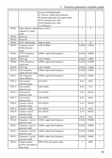
5 Function parameter schedule graph
59
process not holding brake) 47: Vfd run 1 (Run with no electric) 48:Analog input brake line signal output 49:X1 terminal close valid 50:X2 terminal close valid 51~60:Reserve
F09.01 Open collector output terminal Y2 output setup
Same as above 1 0 ×
F09.02 Reserved F09.03 Reserved F09.04 RLY1 output setup Same as above 1 22 × F09.05 Frequency arrival
(FAR) detection range
0.00~50.00Hz 0.01Hz 5.00Hz
F09.06 FDT1 (Frequency level) level
0.00Hz~upper limit frequency 0.01Hz 10.00Hz
F09.07 FDT1 lag 0.00~50.00Hz 0.01Hz 1.00Hz F09.08 FDT2 (Frequency
level) level 0.00Hz~upper limit frequency 0.01Hz 10.00Hz
F09.09 FDT2 lag 0.00~50.00Hz 0.01Hz 1.00Hz F09.10 Zero frequency
signal detection value 0.00Hz~upper limit frequency 0.01Hz 0.00Hz
F09.11 Zero frequency return difference
0.00Hz~upper limit frequency 0.01Hz 0.00Hz
F09.12 Zero-current detection range
0.0~50.0% 0.1% 0.0%
F09.13 Zero-current detection time
0.00~60.00s 0.01s 0.1s
F09.14 Over-current detection value
0.0~250.0% 0.1% 160.0%
F09.15 Over-current detection time
0.00~60.00s 0.01s 0.00s
F09.16 Current 1 arrival detection value
0.0~250.0% 0.1% 100.0%
F09.17 Current 1 width 0.0~100.0% 0.1% 0.0% F09.18 Current 2 arrival
detection value 0.0~250.0% 0.1% 100.0%
F09.19 Current 2 width 0.0~100.0% 0.1% 0.0% F09.20 Frequency 1 arrival
detection value 0.00Hz~upper limit frequency 0.01Hz 50.00Hz
F09.21 Frequency 1 arrival detection width
0.00Hz~upper limit frequency 0.01Hz 0.00Hz
F09.22 Frequency 2 arrival detection value
0.00Hz~upper limit frequency 0.01Hz 50.00Hz
F09.23 Frequency 2 arrival detection width
0.00Hz~upper limit frequency 0.01Hz 0.00Hz
F09.24 Output terminal positive and negative logic setup
0000~FFFF (Extension valid) 1 0000
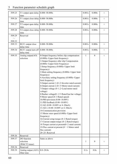
5 Function parameter schedule graph
60
F09.25 Y1 output open delay time
0.000~50.000s 0.001s 0.000s
F09.26 Y1 output close delay time
0.000~50.000s 0.001s 0.000s
F09.27 Y2 output open delay time
0.000~50.000s 0.001s 0.000s
F09.28 Y2 output close delay time
0.000~50.000s 0.001s 0.000s
F09.29 ~
F09.32
Reserved
F09.33 RLY1 output close delay time
0.000~50.000s 0.001s 0.000s
F09.34 RLY1 output turn-off delay time
0.000~50.000s 0.001s 0.000s
F09.35 Analog output(AO) selection
0:Output frequency before slip compensation (0.00Hz~Upper limit frequency) 1:Output frequency after slip Compensation (0.00Hz~Upper limit Frequency) 2:Setup frequency (0.00Hz~Upper limit frequency) 3:Main setting frequency (0.00Hz~Upper limit frequency) 4:Auxiliary setting frequency (0.00Hz~Upper limit frequency) 5:Output current 1 (0~2×Inverter rated current)6:Output current 2 (0~3×Motor rated current) 7:Output voltage (0~1.2×Load motor rated voltage) 8:Busbar voltage(0~1.5×Rated bus bar voltage)9:Motor speed (0~3 Rated speed) 10:PID provision (0.00~10.00V) 11:PID feedback (0.00~10.00V) 12:AI1 (0.00~10.00V or 4~20mA) 13:AI2 (-10.00~10.00V or 4~20mA) 14:Communication provision 15:Motor rotor speed (0.00Hz~Upper limit frequency) 16:Current setup torque (0~2 Rated torque) 17:Current output torque (0~2 Rated torque) 18:Torque current at present(0~2 rated current)19:Flux current at present (0~1 Motor rated flux current) 20~25: Reserved
1 0
F09.36 Reserved F09.37 DO function
selection (With Y2 reuse)
Same as above 1 0
F09.38 Reserved F09.39 Analog output (AO1)
filter time 0.0~20.0s 0.1s 0.0s

5 Function parameter schedule graph
61
F09.40 Analog output (AO1) gain
0.00~2.00 0.01 1.00
F09.41 Analog output (AO1) bias
0.0~100.0% 0.1% 0.0%
F09.42 ~
F09.44
Reserved
F09.45 DO filter time 0.0~20.0s 0.1s 0.0s F09.46 DO output gain 0.00~2.00 0.01 1.00 F09.47 DO maximum pulse
output frequency 0.1~20.0KHz 0.1KH
z 10.0KHz
F09.48 Torque achieve output detection time
0.02~200.00s 0.01s 1.00s
F09.49 Reserved F09.50 Reserved
F10-Simple PLC/Multi-speed Function Parameter Group
Function
code Name Set range
Min.
unit
Factory
default
Modifi-
cationF10.00 Simple PLC run setup LED units digit: run mode selection
0:Inaction 1:Stop after single cycle 2:Final value keep after single cycle 3:Continuous cycle LED tens digit: Interrupt run restart mode selection 0:Restart from first phase 1:Continuous run from phase frequency at interruption 2:Continuous run from run frequency at interruption LED hundreds digit: PLC run time unit 0:Second 1:Minute LED thousands digit: Power-down memory selection 0:No Memory 1:Phase of reserve power down, frequency power down recording PLC run status: contain power down phase, run frequency, time have run.
1 0000 ×
F10.01 Phase 1 setup 000H~E22H LED units digit: Frequency setup 0:Multistage frequency i (i=1~15) 1:Frequency determined by complex frequency of main and auxiliary 2: Reserved LED tens digit: Operation direction selection
1 000

5 Function parameter schedule graph
62
0:Forward 1:Reversal 2:Determine by run command LED hundreds digit: ACC/DEC time selection 0:ACC/DEC time 1 1:ACC/DEC time 2 2:ACC/DEC time 3 3:ACC/DEC time 4 4:ACC/DEC time 5 5:ACC/DEC time 6 6:ACC/DEC time 7 7:ACC/DEC time 8 8:ACC/DEC time 9 9:ACC/DEC time 10 A:ACC/DEC time 11 B:ACC/DEC time 12 C:ACC/DEC time 13 D:ACC/DEC time 14 E:ACC/DEC time 15
F10.02 Phase 2 setup 000H~E22H 1 000 F10.03 Phase 3setup 000H~E22H 1 000 F10.04 Phase 4 setup 000H~E22H 1 000 F10.05 Phase 5 setup 000H~E22H 1 000 F10.06 Phase 6 setup 000H~E22H 1 000 F10.07 Phase 7 setup 000H~E22H 1 000 F10.08 Phase 8 setup 000H~E22H 1 000 F10.09 Phase 9 setup 000H~E22H 1 000 F10.10 Phase 10 setup 000H~E22H 1 000 F10.11 Phase 11 setup 000H~E22H 1 000 F10.12 Phase 12 setup 000H~E22H 1 000 F10.13 Phase 13 setup 000H~E22H 1 000 F10.14 Phase 14 setup 000H~E22H 1 000 F10.15 Phase 15 setup 000H~E22H 1 000 F10.16 Phase 1 run time 0~6000.0 0.1 10.0 F10.17 Phase 2 run time 0~6000.0 0.1 10.0 F10.18 Phase 3 run time 0~6000.0 0.1 10.0
F10.19 Phase 4 run time 0~6000.0 0.1 10.0 F10.20 Phase 5 run time 0~6000.0 0.1 10.0 F10.21 Phase 6 run time 0~6000.0 0.1 10.0 F10.22 Phase 7 run time 0~6000.0 0.1 10.0 F10.23 Phase 8 run time 0~6000.0 0.1 10.0 F10.24 Phase 9 run time 0~6000.0 0.1 10.0 F10.25 Phase 10 run time 0~6000.0 0.1 10.0 F10.26 Phase 11 run time 0~6000.0 0.1 10.0 F10.27 Phase 12 run time 0~6000.0 0.1 10.0 F10.28 Phase 13 run time 0~6000.0 0.1 10.0 F10.29 Phase 14 run time 0~6000.0 0.1 10.0 F10.30 Phase 15 run time 0~6000.0 0.1 10.0

5 Function parameter schedule graph
63
F10.31 Multi-section frequency 1 0.00Hz ~Upper limit frequency 0.01Hz 5.00Hz F10.32 Multi-section frequency 2 0.00Hz ~Upper limit frequency 0.01Hz 10.00Hz F10.33 Multi-section frequency 3 0.00Hz ~Upper limit frequency 0.01Hz 20.00Hz F10.34 Multi-section frequency 4 0.00Hz ~Upper limit frequency 0.01Hz 30.00Hz F10.35 Multi-section frequency 5 0.00Hz ~Upper limit frequency 0.01Hz 40.00Hz F10.36 Multi-section frequency 6 0.00Hz ~Upper limit frequency 0.01Hz 45.00Hz F10.37 Multi-section frequency 7 0.00Hz ~Upper limit frequency 0.01Hz 50.00Hz F10.38 Multi-section frequency 8 0.00Hz ~Upper limit frequency 0.01Hz 5.00Hz F10.39 Multi-section frequency 9 0.00Hz ~Upper limit frequency 0.01Hz 10.00Hz F10.40 Multi-section frequency 10 0.00Hz ~Upper limit frequency 0.01Hz 20.00Hz F10.41 Multi-section frequency 11 0.00Hz ~Upper limit frequency 0.01Hz 30.00Hz F10.42 Multi-section frequency 12 0.00Hz ~Upper limit frequency 0.01Hz 40.00Hz F10.43 Multi-section frequency 13 0.00Hz ~Upper limit frequency 0.01Hz 45.00Hz F10.44 Multi-section frequency 14 0.00Hz ~Upper limit frequency 0.01Hz 50.00Hz F10.45 Multi-section frequency 15 0.00Hz ~Upper limit frequency 0.01Hz 50.00Hz
F11-close loop PID run function parameter group
Function
code Name Set range
Min.
unit
Factory
default
Modifi-
cation
F11.00 Close loop run control selection
0:PID close loop run control invalid 1:PID close loop run control valid
1 0 ×
F11.01 Provide channel selection
0:Digital provide 1:AI1 analog provide 2:AI2 analog provide 3~4:Reserved 5:Pulse provide 6:Communication provide (Add:1D00) 7~8:Reserved
1 0
F11.02 Feedback channel selection
0:AI1 analog input 1:AI2 analog input 2:EAI1 analog input 3:EAI2 analog input 4:AI1+AI2 5:AI1-AI2 6:Min{AI1,AI2} 7:Max{AI1,AI2} 8:Pulse input 9:Communication feedback (Add:1DOC, 4000 represent 10.00V)
1 0
F11.03 Provide channel filtering time
0.01~50.00s 0.01s 0.20s ×
F11.04 Feedback channel filtering time
0.01~50.00s 0.01s 0.10s ×
F11.05 PID output filtering time
0.00~50.00s 0.01s 0.00s
F11.06 Provide digital setup 0.00~10.00V 0.01V 1.00V F11.07 Proportional gain Kp 0.000~9.999 0.001 0.150 F11.08 Integral gain Ki 0.000~9.999 0.001 0.150 F11.09 Differential gain Kd 0.000~9.999 0.001 0.000

5 Function parameter schedule graph
64
F11.10 Sample period T 0.01~1.00s 0.01s 0.10s F11.11 Deviation range 0.0~20.0% correspond to provide value
percentage 0.1% 2.0%
F11.12 PID differential range 0.00~100.00% 0.01% 0.10% F11.13 Close-loop adjust
characteristic 0:Action 1:Reaction
1 0
F11.14 Feedback channel plus-minus characteristic
0:Positive characteristic 1:Negetive characteristic
1 0
F11.15 PID adjusting upper limit frequency
Low limit frequency~ Upper limit frequency 0.01Hz 50.00Hz
F11.16 PID adjusting low limit frequency
Low limit frequency~ Upper limit frequency 0.01Hz 0.00Hz
F11.17 Integral adjusting selection
0:When integral arrival separate PID threshold value, stop integral adjusting 1:When integral arrival separate PID threshold value, continue threshold value adjusting
1 0
F11.18 Integral separate PID threshold value
0.0~100.0% 0.1% 100.0%
F11.19 Close-loop preset frequency
0.00Hz ~upper limit frequency 0.01Hz 0.00Hz
F11.20 Close-loop preset frequency keep time
0.0~6000.0s 0.1s 0.0s
F11.21 Close-loop output changeover selection
0: Close-loop output minus, Low limit frequency run. 1: Cose-loop output minus, Reverse run (Effect by run direction setting ) 2: Comfirmed by run order
1 0
F11.22 Close-loop output frequency maximum value
0.00Hz~upper limit frequency 0.01Hz 50.00Hz
F11.23 Multi-section close-loop provide 1
0.00~10.00V 0.01V 0.00V
F11.24 Multi-section close-loop provide 2
0.00~10.00V 0.01V 0.00V
F11.25 Multi-section close-loop provide 3
0.00~10.00V 0.01V 0.00V
F11.26 Multi-section close-loop provide 4
0.00~10.00V 0.01V 0.00V
F11.27 Multi-section close-loop provide 5
0.00~10.00V 0.01V 0.00V
F11.28 Multi-section close-loop provide 6
0.00~10.00V 0.01V 0.00V
F11.29 Multi-section close-loop provide 7
0.00~10.00V 0.01V 0.00V
F12-Constant Pressure Water Supply Function Parameter Group
Function
code Name Set range
Min.
unit
Factory
default
Modifi-
cation
F12.00 Constant pressure 0:No constant pressure water supply 1 0 ×

5 Function parameter schedule graph
65
water supply mode selection
1~4: Reserved 5: Chooce vfd Y1,Y2 as two pumps time limited rotate work, constant voltage supply water type
F12.01 Target pressure setup 0.000~long-distance pressure gage range 0.001 Mpa
0.200Mpa
F12.02 Sleep frequency minimum value
0.00Hz~Upper limit frequency 0.01Hz 30.00Hz
F12.03 Awake pressure Threshold
0.000~long-distance pressure gage range 0.001 Mpa
0.150Mpa
F12.04 Sleep delay time 0.0~6000.0s 0.1s 0.0s F12.05 Awake delay time 0.0~6000.0s 0.1s 0.0s F12.06 Long-distance
pressure gage range 0.001~9.999Mpa 0.001
Mpa 1.000Mpa
F12.07 Allowed aviation of upper limit frequency and low limit frequency: When add or decrease pump
0.1~100.0% 0.1% 1.0%
F12.08 Pump switching estimate time
0.2~999.9s 0.1s 5.0s
F12.09 Electromagnetism switch converter delay time
0.1~10.0s 0.1s 0.5s
F12.10 Automatically switching time interval
0000~65535 minute 1 0 ×
F12.11 Wake up pattern selection
0: Wake up according to the F12.03 pressure 1: Wake up as the pressure F12.12*F12.01 calculated
1 0
F12.12 Wake up pressure coefficient
0.01~ 0.99 0.01 0.75
F12.13 Reserved F12.14 Reserved
F13-Traverse/ Fixed Length Control Function Parameter Group
Function
code Name Set range
Min.
unit
Factory
default
Modifi-
cation
F13.00 Traverse function enable
0:Traverse invalid 1:Traverse valid
1 0 ×
F13.01 Traverse run mode LED units digit: Enter mode 0:Automatically enter 1:Terminal enter manually LED tens digit: 0:Variable swing 1:Fixed swing LED hundreds digit: Traverse halt start mode selection 0:Restart 1:Start as previous halt record
1 0000 ×

5 Function parameter schedule graph
66
LED thousands digit: traverse status reserve selection 0:No reserve 1:Reserve
F13.02 Traverse frequency swing value
0.0~50.0% 0.1% 10.0%
F13.03 Jump frequency 0.0~50.0% 0.1% 2.0% F13.04 Traverse cycle 0.1~999.9s 0.1s 10.0s F13.05 Triangular wave up
time 0.0~98.0% (Traverse cycle) 0.1% 50.0%
F13.06 Traverse preset frequency
0.00~400.00Hz 0.01Hz 0.00Hz
F13.07 Traverse preset frequency waiting time
0.0~6000.0s 0.1s 0.0s
F13.08 Setup length 0~65535 (m/cm/mm) 1m 0m F13.09 Pulse No. of axis per
circle 1~10000 1 1
F13.10 Axis perimeter 0.01~655.35cm 0.01cm 10.00cm F13.11 Length left percent 0.01~100.00% F13.12 Length correction
coefficient 0.001~10.000 0.001 1.000
F13.13 After length arrival: Record length manage
LED units digit: Reserve LED tens digit: Set length units 0: Meter 1: Cm 2: Mm LED hundreds digit: Act after length fulfill 0: Continue working 1: Recycle limit length control LED hundreds digit: Software reset length(can reset by communication) 0: Keep free 1: The current length is cleared 2: The current and total length both cleared
0 1
F13.14 When stop: Record length manage
LED units digit: Stop and deal with the current length 0: Auto reset 1: Keep length LED tens digit: Power low down length reserve setup 0: No Reserve 1: Reserved LED hundreds digit: Stop and calculate length0: Don’t calculate 1: Calculate
0 1
F14-Vector Control Parameter Group
Function
code Name Set range
Min.
unit
Factory
default
Modifi-
cation
F14.00 Speed/Torque control selection
0: Speed control 1: Torque control (Valid when F00.24=1 or 2)
1 0
F14.01 Speed loop high speed proportional gain
0.1~40.0 (Valid when F00.24=1&2) 0.1 20.0

5 Function parameter schedule graph
67
F14.02 Speed loop high speed integral time
0.001~10.000s (Valid when F00.24=1 or 2) 0.001s 0.040s
F14.03 Speed loop low speed proportional gain
0.1~80.0 (Valid when F00.24=1 or 2) 0.1s 20.0
F14.04 Speed loop low speed integral time
0.001~10.000s (Valid when F00.24=1 or 2) 0.001 Hz
0.020Hz
F14.05 Speed loop parameter switchover frequency
0.00Hz~20.00Hz (Valid when F00.24=1 or 2) 0.01Hz 5.00Hz
F14.06 Low frequency generate electricity stable coefficient
0~50 (Valid when F00.24=1) 1 25
F14.07 Current loop proportional gain
1~500 (Valid when F00.24=1 or 2) 1 70
F14.08 Current loop integral time
0.1~100.0ms (Valid when F00.24=1 or 2) 0.1ms 4.0ms
F14.09 Forward electric torque current limit value(Reverse brake torque current limit)
0.0~250.0% (Valid when F00.24=1 or 2,3) 0.1% 160.0%
F14.10 Forward brake torque current limit value (Reverse electric torque current limit)
0.0~250.0% (Valid when F00.24=1 or 2) 0.1% 160.0%
F14.11 Asynchronous motor low flux control coefficient
20.0~100.0% (Valid when F00.24=1 or 2) 0.1% 80.0%
F14.12 Asynchronous motor min flux coefficient
10.0~80.0% (Valid when F00.24=2) 0.1% 10.0%
F14.13 Setting and limit torque channel selection
LED units digit: Torque setting channel selection 0: Digital setting 1: AI1 analog setting 2: AI2 simulation setting 3:Terminal UP / DOWN adjustment setting 4:Communication setting (Communication address: 1D01) 5: Reserved 6: Reserved 7: High-speed pulse setting (X7 terminal needs to be selected to the corresponding function) 8: Reserved LED Tens digit: Electric torque limit channel selection 0: Digital setting 1: AI1 analog setting 2: AI2 simulation setting 3: Terminal UP/DOWN adjustment setting 4: communication reference (Communication address: 1D01) 5: Reserved 6: Reserved
1 0000 ×

5 Function parameter schedule graph
68
7: High-speed pulse setting (X7 terminal needs to be selected to the corresponding function) 8: Reserved LED hundreds digit: Brake torque limit channel selection 0: Digital setting 1: AI1 analog setting 2: AI2 simulation setting 3: Terminal UP / DOWN adjustment setting 4: Communication setting (Communication address: 1D01) 5: Reserved 6: Reserved 7: High-speed pulse setting (X7 terminal needs to be selected to the corresponding function) 8: Reserved LED thousands digit: Reserved Note: This parameter is valid when F00.24 = 1 or 2.
F14.14 Torque polarity setting
LED units digit: Torque setting polarity 0: Positive 1: Negative 2: Determined by operation command LED tens digit: Torque compensation polarity0: Same as setting torque direction 1: Contrary to the set torque direction LED hundreds digit: F14.21 function is weakened when the motor is stalled 0: Invalid 1: Effective LED thousands digit: Torque control anti-reversing function 0: Invalid 1: Enable torque control the anti-reversing function remains active 2: Only the start moment there is anti-reversal processing Note: This parameter is valid when F00.24 = 1 or 2.
1 0000
F14.15 Torque digital setting value
0.0~200.0% (Valid when F00.24=1&2) 0.1% 0.0%
F14.16 Torque control forward speed limit channel selection
0: Digital setting 1: AI1 analog setting 2: AI2 simulation setting 3: Terminal UP/DOWN adjustment setting 4: Communication reference (Communication address: 1D0A) 5: Reserved 6: Reserved 7: High-speed pulse setting (X7 terminal needs to be selected to the corresponding function) 8: Reserved
1 0 ×

5 Function parameter schedule graph
69
Note: This parameter is valid when F00.24 = 1 or 2.
F14.17 Torque control reverse speed limit channel selection
0: Digital setting 1: AI1 analog setting 2: AI2 simulation setting 3: Terminal UP/DOWN adjustment setting 4: communication reference (Communication address: 1D0B) 5: Reserved 6: Reserved 7: High-speed pulse setting (X7 terminal needs to be selected to the corresponding function) 8: Reserved Note: This parameter is valid when F00.24 = 1 or 2.
1 0 ×
F14.18 Torque control forward speed limit value
0.00Hz~upper limit frequency(Valid when F00.24 = 1 or 2.)
0.01Hz 50.00Hz
F14.19 Torque control reverse speed limit value
0.00Hz~upper limit frequency (Valid when F00.24 = 1 or 2.)
0.01Hz 50.00Hz
F14.20 Set the torque acceleration/ deceleration time
0.000~60.000s (Valid when F00.24 = 1 or 2.) 0.001s 0.100s
F14.21 Torque compensation 0.0~100.0% (Valid when F00.24 = 1 or 2.) 0.1% 5.0% F14.22 Positive torque gain
adjustment coefficient
50.0~150.0% (Valid when F00.24 = 1 or 2.) 0.1% 100.0%
F14.23 Negative torque gain adjustment coefficient
50.0~150.0% (Valid when F00.24 = 1 or 2.) 0.1% 100.0%
F14.24 Flux brake coefficient 0.0~300.0% (Valid when F00.24 = 1 or 2.) 0.1% 0.0%
F14.25 Pre-excitation start time constant
0.1~3.0 (Valid when F00.24 = 1) 0.1 0.5 ×
F14.26 Speed loop proportion gain
0.010~6.000 (Valid when F00.24 = 3.) 0.001 0.500
F14.27 Speed loop integral time constant
0.010~9.999 (Valid when F00.24 = 3.) 0.001 0.360
F14.28 Motor stable coefficient
10~300 (Valid when F00.24 = 3.) 1 100
F14.29 Suppresses the oscillation compensation gain
100.0~130.0% (Valid when F00.24 = 3.) 0.1% 100.0%
F14.30 Torque compensation cutoff frequency
0.00Hz~Upper limit frequency (Valid when F00.24 = 1 or 2.)
0.01Hz 20.00Hz
F15-Asynchronous Motor Parameter Group
Function
code Name Set range
Min.
unit
Factory
default
Modifi-
cation
F15.00 Reserved

5 Function parameter schedule graph
70
F15.01 Asynchronous motor rated power
0.1~6553.5KW 0.1KW Base on motor type
×
F15.02 Asynchronous motor rated voltage
1~690V 1V Base on motor type
×
F15.03 Asynchronous motor rated current
0.1~6553.5A 0.1A Base on motor type
×
F15.04 Asynchronous motor rated frequency
0.00~600.00Hz 0.01Hz Base on motor type
×
F15.05 Asynchronous motor rated speed
0~60000r/min 1r/min Base on motor type
×
F15.06 Asynchronous motor poles No.
1~7 1 2 ×
F15.07 Asynchronous motor stator resistance
0.0000~65.535Ω 0.001Ω Base on motor type
×
F15.08 Asynchronous motor rotor resistance
0.000~65.535Ω 0.001Ω Base on motor type
×
F15.09 Asynchronous motor leakage inductance
0.00~655.35mH 0.01 mH
Base on motor type
×
F15.10 Asynchronous motor mutual inductance
0.00~6553.5mH 0.01mH
Base on motor type
×
F15.11 Asynchronous motor no load current
0.01~655.35A 0.01A Base on motor type
×
F15.12 ~
F15.18
Reserved
F15.19 Motor parameter auto adjustment selection
0: No action 1: Asynchronous motor static self-tuning 2:Asynchronous motor rotation no-load self-tuning 3: Reserved Note:
Before setting, you need to set the ①
nameplate data correctly ② Motor parameter group can be set
according to the type of design automaticallyValue, can also be manually modified, and self-tuning correction.
After modifying the F15.01 parameter, ③
other parameters of the motor will be automatically set to the default value.
1 0 ×
F15.20 ~
F15.22
Reserved
F16-Reserved Parameter Group 1
Function
code Name Set range
Min.
unit
Factory
default
Modifi
-cation
F16.00 Zero servo energy 0:Zero servo invalid 1:Zero servo valid
1 0
F16.01 Coder line number 1~10000 1 1024

5 Function parameter schedule graph
71
F16.02 Coder line direction Unit digit: AB phase sequence 0: Forward direction 1: Rreverse direction Tens digit: Reserved
1 00 ×
F16.03 Coder frequency demultiplication coefficient
0.001~60.000 0.001 1.000
F16.04 Coder smoothing coefficient
5~100 1 15
F16.05 ~
F16.13
Reserved
F17-Reserved Parameter Group 2
Function
code Name Set range
Min.
unit
Factory
default
Modifi-
cationF17.00
~ F17.20
Reserved
F18-Enhance Control Parameter Group
Function
code Name Set range
Min.
unit
Factory
default
Modifi
-cationF18.00 Operation panel
control frequency binding
0: No binding 1: Operation keyboard digital setup 2: AI1 analog setup 3: AI2 analog setup 4: Terminal UP/DOWN adjusting setup 5: Communication provide 6: Reserved 7: Reserved 8: High speed pulse setup (X7 terminal need choose the relative function) 9: Reserved 10:Terminal encoder provide(decide by X1,X2)11~15:Reserved
1 0
F18.01 Terminal control frequency binding
Same as above 1 0
F18.02 Communication control frequency binding
Same as above 1 0
F18.03 Digital frequency integral function selection
LED units digit: Keyboard UP/DW integral control 0: Integral function 1: No integral function LED tens digit: Terminal UP/DW integral control 0: Integral function 1: No integral function
1 00

5 Function parameter schedule graph
72
LED hundreds digit: Keyboard shuttle knob enabled(The shuttle keyboard is valid) 0: In the monitoring interface, the shuttle knob is valid 1: In the monitoring interface, the shuttle knob is invalid LED thousands digit: Keyboard adjustment frequency Classic mode selection 0: Invalid 1: Valid, Adjustment range confirmed by F18.05
F18.04 Keyboard UP/DW integral rate
0.01~50.00Hz 0.01Hz 0.10Hz
F18.05 Keyboard no integral single step’s size setup
0.01~10.00Hz 0.01Hz 0.01Hz
F18.06 Terminal UP/DW integral rate
0.01~50.00Hz 0.01Hz 0.20Hz
F18.07 Terminal no integral single step’s size setup
0.01~10.00Hz 0.01Hz 0.10Hz
F18.08 Droop control decline frequency
0.00~10.00Hz 0.01Hz 0.00Hz
F18.09 Setup accumulate power on time
0~65535h 1 0
F18.10 Setup accumulate run time
0~65535h 1 0
F18.11 Setup run function enable
0: Invalid 1: Valid
1 0
F18.12 Setup run stop time 0.1~6500.0Min 0.1Min 2.0Min F18.13 Currently run arrival
time 0.0~6500.0Min 0.1Min 1.0Min
F18.14 Keyboard UP/DW selection under monitor mode
0:Keyboard frequency provide value adjusting 1:PID digital provide value adjusting 2~6:Reserved
1 0
F18.15 V/F oscillation suppression cutoff frequency
0.00Hz~upper limited frequency 0.01Hz 50.00Hz
F18.16 Advanced control selection
LED units digit: Torque closed loop control enabled 0: Torque open loop control 1: Torque closed loop control LED tens digit: Torque limit mode 0: Rated by the drive rated current 1: Rated by motor rated torque LED hundreds digit: Lower than the lower frequency of fast crossing enable 0: Invalid 1: Effective LED thousands digit: Torque control when low torque reference PWM block is enabled
1 0001

5 Function parameter schedule graph
73
0: Invalid 1: Effective Note: This parameter is valid when F00.24 = 1 or 2
F18.17 Cooling fan control selection
LED units digit: fan control mode 0: Smart fan 1: The inverter has been running after power-on 2: Fan is prohibited, but the temperature is greater than 75 degrees automatically open LED tens digit: adjustable speed fan control mode 0: Intelligent PWM speed control 1: Run at maximum speed
1 00
F18.18 No velocity vector slip gain
50~200% 1% 100%
F18.19 Total power consumption lower position
0~9999 1 degree
0
F18.20 Total power consumption higher position
0~65535(1 represent 10000 degree) 10000 degree
0
F18.21 Power consumption calculate coefficient
50.0%~200.0% 0.1% 100.0%
F18.22 V/F separation control voltage reference channel
0: Number setting (Determined by 18.23) 1: AI1 analog setting 2: AI2 simulation setting 3: Terminal UP/DOWN adjustment setting 4~6: Reserved 7: High speed pulse setting (X7 terminal need to select the corresponding function) 8: Reserved Note: The maximum value of 0 ~ 8 channels corresponds to the motor rated voltage
1 1
F18.23 V/F separation control voltage digital reference channel
0.0%~100% 0.1% 0.0%
F18.24 Reserved 30~300% 1% 100%
F19-Protective Relevant Function Parameter Group
Function
code Name Set range
Min.
unit
Factory
default
Modifi-
cation
F19.00 Power off restart waiting time
0.0~20.0s (0 means no start function) 0.1s 0.0s ×
F19.01 Fault self-recovery times
0~10 (0 means no automatic reset function) 1 0 ×
F19.02 Fault self-recovery interval time
0.5~20.0s 0.1s 5.0s ×

5 Function parameter schedule graph
74
F19.03 Motor overload protection action selection
0:Alarm: continuous run 1:Alarm, Stop run as halt mode 2:Fault, Free halt
1 2 ×
F19.04 Motor overload protection coefficient
20.0~120.0%(motor rated current) 0.1% 100.0% ×
F19.05 Inverter overload pre-alarm detection selection
0:Detection all the time 1:Detection as constant velocity
1 0 ×
F19.06 Inverter overload pre-alarm detection level
20~180% (Inverter rated current) 1% 130%
F19.07 Inverter overload pre-alarm delay time
0.0~20.0s 0.1s 5.0s
F19.08 Motor under-load alarm detection level
0.0~120.0% (Motor rated current) 0.1% 50.0%
F19.09 Motor under-load alarm detection time
0.1~60.0s 0.1s 2.0s
F19.10 Motor under-load alarm detection action
LED units digit: detection selection 0:No detection 1:Detection all the time when run 2:Detection only when constant velocity LED tens digit: Action selection 0:Alarm, continuous run 1:Alarm, stop run as halt mode 2:Fault, free halt
1 00
F19.11 Input& output phase loss, short circuit detection action
LED units digit: Input phase loss 0:No detection 1:Fault, free halt LED tens digit: Output phase loss 0:No detection 1:Fault, free halt LED hundreds digit: Power-on on earth short circuit protect detection enable 0:No detection 1:Fault, free halt LED thousands digit: Operation on earth short circuit protect detection enable 0:No detection 1:Fault, free halt
1 1111
F19.12 Overvoltage stall selection
0:Forbid 1:Allowed
1 1 ×
F19.13 Overvoltage stall protection voltage
100~150% 1% 125% ×
F19.14 Automatic current limit level
110~230%, G type rated current 1% 170% ×
F19.15 Frequency decline rate of automatic current limit
0.00~99.99Hz/s 0.01Hz/s 10.00Hz/s ×
F19.16 Automatic current limit action selection
0:Constant velocity invalid 1:Constant velocity valid
1 0 ×
F19.17 Reserved

5 Function parameter schedule graph
75
F19.18 Motor run section selection when instant power off
0:Forbid 1:Allowed
1 0 ×
F19.19 Frequency droop rate when instant power off
0.00~99.99Hz/s 0.01Hz/s 10.00Hz/s ×
F19.20 Voltage rebound estimate time when instant power off
0.00~10.00s 0.01s 0.10s ×
F19.21 Action estimate voltage when instant power off
60~100% (Rated bus bar voltage) 1% 80% ×
F19.22 Allowed the longest off time when instant power off
0.30~5.00s 0.01s 2.00s ×
F19.23 Terminal external device fault action selection
0:Alarm, Continuous run 1:Alarm, Stop run as halt mode 2:Fault, Free halt
1 2 ×
F19.24 Power on terminal protection selection
0:Invalid 1:Valid
1 1 ×
F19.25 Provide lost detection value
0~100% 1% 0%
F19.26 Provide lost detection time
0.0~500.0s 0.1s 0.5s
F19.27 Feedback lost detection value
0~100% 1% 12%
F19.28 Feedback lost detection time
0.0~500.0s 0.1s 0.5s
F19.29 Deviation magnitude abnormal detection value
0~100% 1% 50%
F19.30 Deviation magnitude abnormal detection time
0.0~500.0s 0.1s 0.5s
F19.31 Protection action selection 1
LED units digit: PID provide loss detection act0:No detection 1:Alarm, Continue run 2:Alarm, Stop run as halt mode 3:Fault, Free halt LED tens digit: PID feedback loss detection act0:No detection 1:Alarm, Continue run 2:Alarm, Stop run as halt mode 3:Fault,Free halt LED hundreds digit: PID error value abnormal detect action 0:No detection 1:Alarm, Continue run 2:Alarm, Stop run as halt mode 3:Fault, Free halt
1 000
F19.32 Protection action LED units digit: Communication abnormal 1 1200 ×

5 Function parameter schedule graph
76
selection 2 action: Include communication time out and error 0:Alarm, continue run 1:Alarm, stop run as halt mode 2:Fault, free halt LED tens digit: E2PROM abnormal action selection 0:Alarm, continue run 1:Alarm, stop run as halt mode 2:Fault, free halt LED hundreds digit: Contactor abnormal action 0:Alarm, Continue run 1:Alarm, Stop run as halt mode 2:Fault, Free halt LED thousands digit: Undervoltage fault indication action selection 0:No detection 1:Fault, Free halt
F19.33 Reserved F19.34 Reserved F19.35 Fault indication and
clock during the period of recovery
LED units digit: Fault indication selection during the period of fault reset automatically 0:Action 1:No action LED tens digit: Fault clock function selection: to achieve fault display before power down: etc. 0:Forbid 1:Open
1 00 ×
F19.36 Continuous run frequency selection when alarm
Match up with protect action 0: Run at the frequency setup by now 1: Run at the frequency of upper limit 2: Run at the frequency of low limit 3:Run at the frequency of abnormal for standby
1 0 ×
F19.37 Abnormal standby frequency
0.00Hz~upper limit frequency 0.01Hz 10.00Hz ×
F19.38 Coder brake line detect time
0.0~8.0s (No detected at 0) 0.01Hz 10.00Hz
F19.39 Over speed (OS) detection value
0.0~120.0% (Corresponding to upper limited frequency)
0.1s 0.0s
F19.40 Over speed (OS) detection time
0.00~20.00s (No detected at 0) 0.1% 120.0%
F19.41 Speed deviate too large (DEV) detection value
0.0~50.0% (Corresponding to upper limited frequency) 0.01s 0.00s
F19.42 Speed deviate too large (DEV) detection time
0.00~20.00s (No detected at 0) 0.1% 10.0%
F19.43 Over voltage suppression
0.0~100.0% 0.01s 0.00s

5 Function parameter schedule graph
77
coefficient F19.44 Reserved
F20-Internal Virtual Input Output Node Parameter Group
Function
code Name Set range
Min.
unit
Factory
default
Modifi-
cation
F20.00 Virtual input VDI1 function selection
0~90 1 0
F20.01 Virtual input VDI2 function selection
0~90 1 0
F20.02 Virtual input VDI3 function selection
0~90 1 0
F20.03 Virtual input VDI4 function selection
0~90 1 0
F20.04 Virtual input VDI5 function selection
0~90 1 0
F20.05 Virtual output VDO1 function selection
0~60 1 0
F20.06 Virtual output VDO2 function selection
0~60 1 0
F20.07 Virtual output VDO3 function selection
0~60 1 0
F20.08 Virtual output VDO4 function selection
0~60 1 0
F20.09 Virtual output VDO5 function selection
0~60 1 0
F20.10 Virtual output VDO1 open delay time
0.00~600.00s 0.01s 0.00s
F20.11 Virtual output VDO2 open delay time
0.00~600.00s 0.01s 0.00s
F20.12 Virtual output VDO3 open delay time
0.00~600.00s 0.01s 0.00s
F20.13 Virtual output VDO4 open delay time
0.00~600.00s 0.01s 0.00s
F20.14 Virtual output VDO1 open delay time
0.00~600.00s 0.01s 0.00s
F20.15 Virtual output VDO1 close delay time
0.00~600.00s 0.01s 0.00s
F20.16 Virtual output VDO2 close delay time
0.00~600.00s 0.01s 0.00s
F20.17 Virtual output VDO3 close delay time
0.00~600.00s 0.01s 0.00s
F20.18 Virtual output VDO4 close delay time
0.00~600.00s 0.01s 0.00s
F20.19 Virtual output VDO5 close delay time
0.00~600.00s 0.01s 0.00s
F20.20 Virtual input VDI enable control
00~FF 1 00
F20.21 Virtual input VDI status 00~FF 1 00

5 Function parameter schedule graph
78
digital setup F20.22 Virtual input: output
connection 00~FF Bit0:VDI1 and VDO1 connection 0: Positive logic 1: Negative logic Bit1:VDI2 and VDO2 connection 0: Positive logic 1: Negative logic Bit3:VDI3 and VDO3 connection 0: Positive logic 1: Negative logic Bit4:VDI4 and VDO4 connection 0: Positive logic 1: Negative logic Bit4:VDI5 and VDO5 connection 0: Positive logic 1: Negative logic
1 00
F21-Reserved Parameter Group 3
Function
code Name Set range
Min.
unit
Factory
default
Modifi-
cationF21.00
~ F21.21
Reserved
F22-Reserved Parameter Group 4
Function
code Name Set range
Min.
unit
Factory
default
Modifi-
cationF22.00
~ F22.17
Reserved
F23-Reserved Parameter Group 5
Function
code Name Set range
Min.
unit
Factory
default
Modifi-
cationF23.00
~ F23.17
Reserved
F24-Reserved Parameter Group 6
Function
code Name Set range
Min.
unit
Factory
default
Modifi-
cationF24.00
~ F24.13
Reserved
F25-User Definition Display Parameter Group
Function
code Name Set range
Min.
unit
Factory
default
Modifi-
cationF25.00 User function code 1 F00.00~F25.xx 0.01 25.00 F25.01 User function code 2 F00.00~F25.xx 0.01 25.00
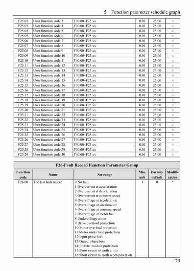
5 Function parameter schedule graph
79
F25.02 User function code 3 F00.00~F25.xx 0.01 25.00 F25.03 User function code 4 F00.00~F25.xx 0.01 25.00 F25.04 User function code 5 F00.00~F25.xx 0.01 25.00 F25.05 User function code 6 F00.00~F25.xx 0.01 25.00 F25.06 User function code 7 F00.00~F25.xx 0.01 25.00 F25.07 User function code 8 F00.00~F25.xx 0.01 25.00 F25.08 User function code 9 F00.00~F25.xx 0.01 25.00 F25.09 User function code 10 F00.00~F25.xx 0.01 25.00 F25.10 User function code 11 F00.00~F25.xx 0.01 25.00 F25.11 User function code 12 F00.00~F25.xx 0.01 25.00 F25.12 User function code 13 F00.00~F25.xx 0.01 25.00 F25.13 User function code 14 F00.00~F25.xx 0.01 25.00 F25.14 User function code 15 F00.00~F25.xx 0.01 25.00 F25.15 User function code 16 F00.00~F25.xx 0.01 25.00 F25.16 User function code 17 F00.00~F25.xx 0.01 25.00 F25.17 User function code 18 F00.00~F25.xx 0.01 25.00 F25.18 User function code 19 F00.00~F25.xx 0.01 25.00 F25.19 User function code 20 F00.00~F25.xx 0.01 25.00 F25.20 User function code 21 F00.00~F25.xx 0.01 25.00 F25.21 User function code 22 F00.00~F25.xx 0.01 25.00 F25.22 User function code 23 F00.00~F25.xx 0.01 25.00 F25.23 User function code 24 F00.00~F25.xx 0.01 25.00 F25.24 User function code 25 F00.00~F25.xx 0.01 25.00 F25.25 User function code 26 F00.00~F25.xx 0.01 25.00 F25.26 User function code 27 F00.00~F25.xx 0.01 25.00 F25.27 User function code 28 F00.00~F25.xx 0.01 25.00 F25.28 User function code 29 F00.00~F25.xx 0.01 25.00 F25.29 User function code 30 F00.00~F25.xx 0.01 25.00
F26-Fault Record Function Parameter Group
Function
code Name Set range
Min.
unit
Factory
default
Modifi-
cationF26.00 The last fault record 0:No fault
1:Overcurrent at acceleration 2:Overcurrent at deceleration 3:Overcurrent at constant speed 4:Overvoltage at acceleration 5:Overvoltage at deceleration 6:Overvoltage at constant speed 7:Overvoltage at motor halt 8:Undervoltage at run 9:Drive overload protection 10:Motor overload protection 11:Motor under load protection 12:Input phase loss 13:Output phase loss 14:Inverter module protection 15:Short circuit to earth at run 16:Short circuit to earth when power on
1 0 *

5 Function parameter schedule graph
80
17:Drive overheat 18:External device fault 19:Current detect circuit fault 20:External interference 21:Internal interference-main clock etc 22:PID provide lost 23:PID feedback lost 24:PID error value abnormal 25:Terminal protection activate 26:Communication fault 27~29:Reserve 30:E2ROM read-write error 31:Temperature detection disconnection 32:Auto-tunning fault 33:Contactor abnormal 34:Factory fault 1 35:Factory fault 2 36:Reserved 37:Coder broke line 38:Over speed protection 39:Speed deviate too large protection 40:Z purse missing fault 41:Analog channel broke line protection42~50: Reserved
F26.01 The last two fault records Same as above 1 0 * F26.02 The last three fault records Same as above 1 0 * F26.03 The last four fault records Same as above 1 0 * F26.04 Setup frequency at the last
one fault 0.00Hz~Upper limit frequency 0.01Hz 0 *
F26.05 Output frequency at the last one fault
0.00Hz~Upper limit frequency 0.01Hz 0 *
F26.06 Output current at the last one fault
0.0~6553.5A 0.1A 0.0A *
F26.07 DC bus voltage at the last one fault
0.0~6553.5V 0.1V 0.0V *
F26.08 Module temperature at the last one fault
0~125 1 0 *
F26.09 Input terminal status at the last one fault
0 *
F26.10 Accumulated run time at the last one fault
0~65535h 1h 0 *
F26.11 Setup frequency at the last two fault
0.00Hz~Upper limit frequency 0.01Hz 0.00Hz *
F26.12 Output frequency at the last two fault
0.00Hz~Upper limit frequency 0.01Hz 0.00Hz *
F26.13 Output current at the last two fault
0.0~6553.5A 0.1A 0.0A *
F26.14 DC bus voltage at the last two fault
0.0~6553.5V 0.1V 0.0V *
F26.15 Module temperature at the last two fault
0~125 1 0 *

5 Function parameter schedule graph
81
F26.16 Input terminal status at the last two fault
0 *
F26.17 Accumulated run time at the last two fault
0~65535min 1min 0min *
F27-Password and Manufacturer Function Parameter Group
Function
code Name Set range
Min.
unit
Factory
default
Modific
ation
F27.00 User password 00000~65535 1 00000 F27.01 Manufacturer password 00000~65535 1 00000
C-Monitor Function Parameter Group
Function
code Name Set range
Min.
unit
Factory
default
Modifi-
cationC-00 Display the parameter of
F00.01, F00.07 definition
C-01 Display the parameter of F00.02, F00.08 definition
C-02 Display the parameter of F00.03, F00.09 definition
C-03 Display the parameter of F00.04, F00.10 definition
C-04 Display the parameter of F00.05, F00.11 definition
C-05 Display the parameter of F00.06, F00.12 definition
(1) Corresponding relationship of input terminal status as below:
X3 terminal status Reserved
Reserved Reserved
X7 terminal status X6 terminal status
X5 terminal status
X4 terminal status
X2 terminal status
X1 terminal status
: terminal input invalid
: terminal input valid
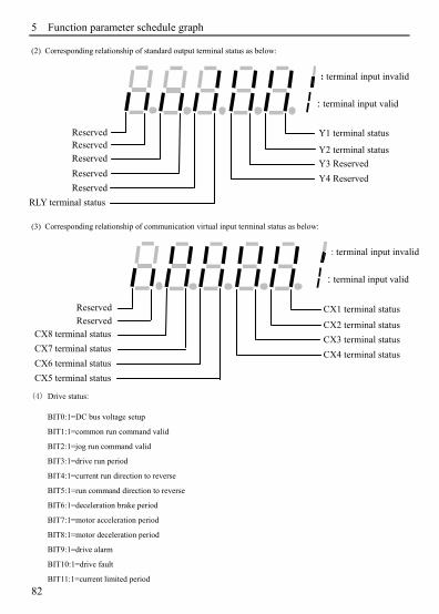
5 Function parameter schedule graph
82
(2) Corresponding relationship of standard output terminal status as below:
(3) Corresponding relationship of communication virtual input terminal status as below:
(4) Drive status:
BIT0:1=DC bus voltage setup
BIT1:1=common run command valid
BIT2:1=jog run command valid
BIT3:1=drive run period
BIT4:1=current run direction to reverse
BIT5:1=run command direction to reverse
BIT6:1=deceleration brake period
BIT7:1=motor acceleration period
BIT8:1=motor deceleration period
BIT9:1=drive alarm
BIT10:1=drive fault
BIT11:1=current limited period
: terminal input invalid
: terminal input valid
CX8 terminal status
Reserved Reserved
CX7 terminal status
CX6 terminal status
CX5 terminal status
CX4 terminal status
CX3 terminal status
CX2 terminal status
CX1 terminal status
RLY terminal status
: terminal input invalid
: terminal input valid
Reserved Reserved Reserved Reserved Reserved
Y4 Reserved
Y3 Reserved Y2 terminal status
Y1 terminal status

5 Function parameter schedule graph
83
BIT12:1=fault self-recovery period
BIT13:1=self-adjusting period
BIT14:1=free halt status
BIT15:1=speed tracking start

6 Troubleshooting
84
6 Troubleshooting
6.1 Failure and countermeasure Possible failure types in EN630/EN650A are shown in Table 6-1, the fault types
including fault and alarm. Such as if inverter fault display E-XX , while the corresponding alarm is displayed in A-XX . Once the inverter failure , fault types are stored in the F26 fault recording parameter group, and if alarm, alarm status has been revealed, until the alarm source release, alarm status are not logged to the F26 parameter group. Some failure code is reserved for intelligent automatic diagnosis function which will be executed continuously in future. When failure takes place in the inverter, the user should check according to note of this table first and record failure phenomena detailedly. Please contact our after-sale service and technical support Department or agent in your local place when technical service is needed.
Table 6-1 Failure type and the countermeasure Failure
code Failure type Possible reason Countermeasure
E-01
Overcurrent during accelerating process
Accelerating time is too short
Prolong accelerating time
Improper V/F curve Adjust V/F curve setting, adjust manual torque boost or change to automatic torque boost
Restart rotating motor Set speed checking restart function
Low power source voltage Check input power supply
Too small power of the inverter
Choose inverter with higher power
Output phase lose under vector control
Check whether the motor wiring is in good condition
E-02
Overcurrent during decelerating process
Decelerating time is too short
Prolong decelerating time
Have potential energy load or big inertia load
Increase braking power of external energy consumption braking subassembly
Power of inverter is a bit small
Choose inverter with higher power
E-03 Overcurrent during constant speed process
Load change suddenly or have unwonted phenomena
Check or reduce break of the load
Acc/Dec. time is set too short
Prolong accelerating decelerating time properly
Low power source voltage Check input power supply

6 Troubleshooting
85
Power of inverter is a bit small
Choose inverter with higher power
E-04
Overvoltage during accelerating process
Unwonted input voltage Check input power supply
Acc time is set too short Prolong accelerating time properly
Restart rotating motor Set speed checking restart function
E-05
Overvoltage during decelerating process
Decelerating time is too short
Prolong decelerating time
Have potential energy load or big inertia load
Increase braking power of external energy consumption braking subassembly
E-06 Overvoltage during constant speed process
Unwonted input voltage Check input power supply
Acc./Dec. time is set too short
Prolong accelerating decelerating time properly
Input voltage change abnormally
Assemble input reactor
Load inertia is a bit big Use energy consumption subassembly
E-07 Overvoltage when stopped
Unwonted input voltage Check input power supply or look for service
E-08 Low-voltage when running
Input voltage is too low Check the input voltage
E-09 Inverter overload protection
Acc time is set to too short Prolong accelerating time
DC braking is too big Reduce DC braking Current, prolong braking time
Improper V/F curve Adjust V/F curve and torque boost
Restart rotating motor Set speed checking restart function
Power source voltage is too low
Check power source voltage
Load is too big Choose inverter with higher power
E-10 (A-10)
Motor overload protection
Improper V/F curve Adjust V/F curve and torque boost
Power source voltage is too low
check power source voltage
General motor run at low speed with big load
Can choose frequency conversion motor for long time low speed run

6 Troubleshooting
86
Motor overload protection factor set incorrectly
to set motor overload protectionfactor correctly
Motor blocked up or load change too suddenly and quickly
Check the load
E-11 (A-11)
Motor under-load protection
The operating current of inverter less than under-load threshold
Confirm whether the parameters F19.08,F19.09 setting are reasonable
load divorced from motor Checking whether the load divorced from motor
E-12 The input phase lose
The three-phase input power supply is abnormal
Check the three-phase input power line is off or poor contact
Power supply board anomaly
Look for service from manufacturer or agent
The control board anomaly Look for service from manufacturer or agent
E-13 The output phase lose
The cable from inverter to motor anomaly
Checking the cable
When the motor runs inverter three-phase output unbalanced
Check whether the motor three-phase winding is balance
Power supply board anomaly
Look for service from manufacturer or agent
The control board anomaly Look for service from manufacturer or agent
E-14 Inverting module protection
Transient overcurrent of the inverter
Refer to countermeasure for overcurrent
phase to phase short circuit or earthing short circuit of output 3 phase
wiring again
Air-path blocked or fan damaged
To clear air-path or replace the fan
Ambient temperature is too high
Lower ambient temperature
Connecting wire or insert on control board loose
Check and connect the wire again
Unwonted current wave caused by missing output phase etc.
Check wiring
Assistant power supply damaged and drive voltage lacking
Look for service from manufacturer or agent

6 Troubleshooting
87
Unwonted control board Look for service from manufacturer or agent
E-15 Short circuit to ground when operation
Motor short circuit to ground
The replacement of cable or motor
Hall component is damaged or the hall wiring is poor or the current detection circuit is abnormal
Look for service from manufacturer or agent
E-16 Short circuit to ground when power on
Motor short circuit to ground
Change the cable or motor
The power supplier of the inverter and the motor wiring are reversed
Change the cable or motor wiring
Hall component is damaged or the hall wiring is poor
Look for service from manufacturer or agent
E-17 (A-17)
Inverter overheat
Duct blockage Cleaning or to improve the ventilation duct
The ambient temperature is too high
To improve the ventilation conditions, decreasing the carrier frequency
Fan damage Change new one
External fault emergency stop terminal closed
External fault disconnect after external fault terminal
E-18 (A-18)
External device failure
Sudden stop terminal for external failure closed
Open external failure terminal after external failure is settled
E-19 Current detecting circuit failure
Connecting wire or insert on control board loose
Check and connect the wire again
Assistant power supply damaged
Look for service from manufacturer or agent
Hall component damaged Look for service from manufacturer or agent
Unwonted amplifying circuit
Look for service from manufacturer or agent
E-20 External interference failure
External disturbance serious
Press "STOP/RESET" button to reset or add external power supply filter from power input side
E-21 External interference failure
External disturbance seriousPower off and restart, if the failure persists, seek the manufacturer or dealer service
E-22(A-22)
PID Given loss PID given loss threshold setting is not reasonable
To reset the relevant parameters
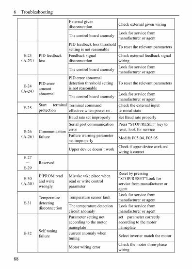
6 Troubleshooting
88
External given disconnection
Check external given wiring
The control board anomalyLook for service from manufacturer or agent
E-23 (A-23)
PID feedback loss
PID feedback loss threshold setting is not reasonable
To reset the relevant parameters
Feedback signal disconnection
Check external feedback signal wiring
The control board anomalyLook for service from manufacturer or agent
E-24 (A-24)
PID error amount abnormal
PID error abnormal detection threshold setting is not reasonable
To reset the relevant parameters
The control board anomalyLook for service from manufacturer or agent
E-25 Start terminal protection
Terminal command effective when power on .
Check the external input terminal state
E-26 (A-26)
Communication failure
Baud rate set improperly Set Baud rate properly
Serial port communication error
Press “STOP/RESET” key to reset, look for service
Failure warning parameter set improperly
Modify F05.04, F05.05
Upper device doesn’t workCheck if upper device work and wiring is correct
E-27 ~
E-29 Reserved
E-30 (A-30)
E2PROM read and write wrongly
Mistake take place when read or write control parameter
Reset by pressing “STOP/RESET”Look for service from manufacturer or agent
E-31 Temperature detecting disconnection
Temperature sensor fault Look for service from manufacturer or agent
The temperature detection circuit anomaly
Look for service from manufacturer or agent
E-32 Self tuning failure
Parameter setting not according to the motor nameplate
set parameter correctly according to the motor nameplate
current anomaly when tuning
Select inverter match the motor
Motor wiring error Check the motor three-phase wiring
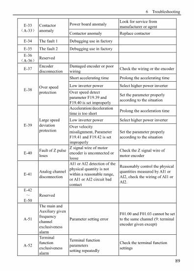
6 Troubleshooting
89
E-33 (A-33)
Contactor anomaly
Power board anomaly Look for service from manufacturer or agent
Contactor anomaly Replace contactor
E-34 The fault 1 Debugging use in factory
E-35 The fault 2 Debugging use in factory
E-36 (A-36)
Reserved
E-37 Encoder disconnection
Damaged encoder or poor wiring
Check the wiring or the encoder
E-38 Over speed protection
Short accelerating time Prolong the accelerating time
Low inverter power Select higher power inverter
Over speed detect parameter F19.39 and F19.40 is set improperly
Set the parameter properly according to the situation
E-39 Large speed deviation protection
Acceleration/deceleration time is too short
Prolong the acceleration time
Low inverter power Select higher power inverter
Over velocity misalignment, Parameter F19.41 and F19.42 is set improperly
Set the parameter properly according to the situation
E-40 Fault of Z pulse loses
Z signal wire of motor encoder is unconnected or loose
Check the Z signal wire of motor encoder
E-41 Analog channel disconnection
AI1 or AI2 detection of the physical quantity is not within a reasonable range, or AI1 or AI2 circuit bad contact
Reasonably control the physical quantities measured by AI1 or AI2, check the wiring of AI1 or AI2.
E-42 ~
E-50 Reserved
A-51
The main and Auxiliary given frequency channel exclusiveness alarm
Parameter setting error F01.00 and F01.03 cannot be set to the same channel (9: terminal encoder given except)
A-52
Terminal function exclusiveness alarm
Terminal function parameters setting repeatedly
Check the terminal function settings

6 Troubleshooting
90
A-53 Run limit alarm Reach limited running time Please contact your supplier
LOCH1. Keypad lock Keypad buttons lock Check chapter 4.2.6
6.2 Failure record lookup This series inverter can record latest 4 failure code and inverter run parameter of
the last 2 times failure, to search these information can redound to finding out reason of the failure.
Failure information is all stored in F26 group parameter,please enter into F26 group parameter to see about information by referring to keypad operation method.
Code Content Code Content
F26.00 Previous one failure record F26.09 Input terminal state at previous failure
F26.01 Previous two failure record F26.10 Total running time at previous failure
F26.02 Previous three failure record F26.11 Set freq. at previous 2 failure
F26.03 Previous four failure record F26.12 Output freq. at previous 2 failure
F26.04 Set freq. at previous failure F26.13 Output current. at previous 2 failure
F26.05 Output freq. at previous failure F26.14 DC bus volt. at previous 2 failure
F26.06 Output current. at previous failure F26.15 Module temp. at previous 2 failure
F26.07 DC bus volt. at previous failure F26.16 Input terminal state of previous 2 failure
F26.08 Module temp. at previous failure F26.17 Total running time of previous 2 failure
(1)Alarm fault of E-16, the inverter must be power off for reset. (2)For the faults of over-current, short-circuit to ground while running, inverter can reset after 2s delay. Note

6 Troubleshooting
91
6.3 Failure reset
To resume normal running when failure takes place in the inverter, you can
choose following any kind of operation:
(1)After you set any terminal of X1~X8 to be inputted by external RESET, it
will be disconnected after connected to COM.
(2)When failure code is displayed, press key after restoration is
confirmed.
(3)Communication reset. Please refer to annex description.
(4)Cut off power supply.
6.4 Alarm reset
When an alarm occurs, must eliminate alarm source which cause alarm, otherwise the alarm can not be eliminated, also cannot be reset by reset button.
STOPRESET
(1) Before reset you must find out reason of failure downright and eliminate it, otherwise may cause permanent damage to the inverter. (2) If can’t reset or failure takes place again after resetting, should look for reason and continuous resetting will damage the inverter. (3) Reset should take place 5 minutes later after overload, overheat protection action. (4) For the failure of E-14, the reset is invalid, the motor wiring should be checked after power off, and restart the inverter. (5) When there is a fault of E-16 after power on, do not directly run the inverter after reset, and need to check whether the input, out wiring are reversed.
!
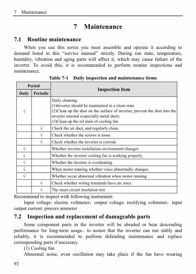
7 Maintenance
92
7 Maintenance
7.1 Routine maintenance When you use this series you must assemble and operate it according to
demand listed in this “service manual” strictly. During run state, temperature, humidity, vibration and aging parts will affect it, which may cause failure of the inverter. To avoid this, it is recommended to perform routine inspections and maintenance.
Table 7-1 Daily inspection and maintenance items
Period Inspection item
Daily Periodic
√
Daily cleaning: (1)Inverter should be maintained in a clean state (2)Clean up the dust on the surface of inverter, prevent the dust into the inverter internal (especially metal dust). (3)Clean up the oil stain of cooling fan
√ Check the air duct, and regularly clean.
√ Check whether the screws is loose
√ Check whether the inverter is corrode
√ Whether inverter installation environment changes
√ Whether the inverter cooling fan is working properly
√ Whether the inverter is overheating
√ When motor running whether voice abnormally changes.
√ Whether occur abnormal vibration when motor running
√ Check whether wiring terminals have arc trace
√ The main circuit insulation test
Recommend to inspect with following instrument: Input voltage: electric voltmeter;output voltage: rectifying voltmeter;input
output current: pincers ammeter
7.2 Inspection and replacement of damageable parts Some component parts in the inverter will be abraded or bear descending
performance for long-term usage,to assure that the inverter can run stably and reliably, it is recommended to perform defending maintenance and replace corresponding parts if necessary.
(1) Cooling fan Abnormal noise, even oscillation may take place if the fan have wearing

7 Maintenance
93
bearing, aging blade, here replacement of the fan should be considered. (2) Filter electrolyte capacitance When frequent-changing load causes increasing pulsating current and aging
electrolyte under high ambient temperature, the electrolyte capacitance may be damaged and here should replace it.
7.3 Repair guarantee (1) We provide the free maintenance within warranty time if any failure or
damage under normal usage, the warranty time can be seen in the warranty card, we will charge some when exceed warranty time.
(2) We will take some upkeep if one of following situations takes place within period of repair guarantee.
a. If did not use the inverter according to<Service manual>strictly or did not use it under ambient demanded in<Service manual>, which cause failure.
b. Failure caused by applying the inverter to non-normal function; c. Failure caused by self-repair, refit which is not already allowed; d. Damage caused by bad keeping, falling down from high place or other
extrinsic factor after purchasing the inverter; e. Failure caused by natural disaster or its reason such as unwonted voltage,
thunderbolt, water fog, fire, salt corroding, gas corroding, earthquake and storm etc.; f. Make bold to tear up product logo (Such as: nameplate etc.); Body serial
number don’t accord with that in repair guarantee card. (3) We calculate service fee based on actual cost, which is subject to contract if
any. (4) You can contact the agent and also our company directly if you have
questions. After repair guarantee period, we shall also provide lifetime charged repair service for our products.
7.4 Storage The user must pay attention to following points for temporary storage and
long-term storage after purchasing the inverter: (1) Avoid storing the inverter in high temperature, moist place and place of dust,
metal powder and assure good ventilation. (2) Longtime storage will cause low quality of electrolyte capacitance, so must
assure that it’s electrified for one time within 1 year and electrification time is not shorter than 1 hour and input voltage must be increased to rated value gradually by voltage regulator of 250w, meanwhile the inverter should be cut off from the motor.
Our company will also provide lifetime repair service with fee for inverter which is not within period of repair guarantee.
Note
Appendix A EN650A Mini multi-function PMSM Inverter
94
Appendix A EN650A Mini multi-function PMSM Inverter
A.1 Symbol description × ---- parameter can’t be changed in process of running ---- parameter can be changed in process of running * ---- read-only parameter, unchangeable
A.2 Function parameter schedule graph
F00-System Parameter Group
Function code
Name Set range Min. unit
FactoryDefault
Modifi-cation
F00.00 Parameter group display control
0: Basic list mode (Only display F00~F03 basic control parameter group and F26 fault record parameter group.) 1: Middle list mode. Display all parameter except for extension: virtual and reserve parameter group. 2: Senior list mode. All parameter display.3: User list mode. Display parameter defined by user: and monitor parameter: F00.00 display all the time. Note: Under mode 1, some related parameters would be hidden according to motor and control mode.
1 0
F00.01 C-00 display parameter selection when operation
0:Main setup frequency (0.01Hz) 1:Auxiliary setup frequency (0.01Hz) 2:Setup frequency (0.01Hz) 3:Output frequency (0.01Hz) 4:Output current (0.1A) 5:Output voltage (1V) 6:DC bus voltage (0.1V) 7:Motor speed (1 circle/min) 8:Motor line velocity (1 circle/min) 9:Inverter temperature (1) 10:Run time already this time (0.1min) 11:Current accumulate run time (1h) 12:Current accumulate power-on time (1h)13:Inverter status 14:Input terminal status 15:Output terminal status (Standard) 16:Extension output terminal status 17:Extension input terminal status 18:Communication virtual input terminal status 19:Internal virtual input node status 20:Analog input AI1(After checkout) (0.01V/0.01mA)
1 3

Appendix A EN650A Mini multi-function PMSM Inverter
95
21:Analog input AI2(After checkout) (0.01V/0.01mA) 22:Extension analog input EAI1(after checkout) (0.01V/0.01mA) 23:Extension analog input EAI2(after checkout) (0.01V/0.01mA) 24:Analog AO1 output(after checkout) (0.01V/0.01mA) 25:Analog AO2 output(after checkout) (0.01V/0.01mA) 26:Extension analog EAO1 output (0.01V /0.01mA) 27: Extension analog EAO2 output (0.01V /0.01mA) 28:External pulse input frequency(before checkout)(1Hz) 29:Reserved 30:Process PID provide(0.01V) 31:Process PID feedback(0.01V) 32:Process PID deviation(0.01V) 33:Process PID output(0.01Hz) 34: Simple PLC current segment No. 35: External multi-speed current segment No. 36:Reserved 37:Reserved 38:Reserved 39:Current length(1M) 40:Accumulate length(1M) 41:Current internal count value 42:Current internal time value(0.1s) 43:run command setup channel(0:keyboard1:terminal 2:communication) 44:main frequency provide channel 45:auxiliary frequency provide channel 46:rated current(0.1A) 47:rated voltage(1V) 48:rated power(0.1KW) 49:Inverter provision torque(percentage of rated torque with direction) 50:Inverter output torque (1 N.M) 51~65:Reserved
F00.02 C-01 display parameter selection when operation
Same as above 1 2
F00.03 C-02 display parameter selection when operation
Same as above 1 4
F00.04 C-03 display parameter selection when operation
Same as above 1 5
F00.05 C-04 display parameter Same as above 1 6
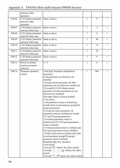
Appendix A EN650A Mini multi-function PMSM Inverter
96
selection when operation
F00.06 C-05 display parameter selection when operation
Same as above 1 9
F00.07 C-00 display parameter selection when stop
Same as above 1 2
F00.08 C-01 display parameter selection when stop
Same as above 1 6
F00.09 C-02 display parameter selection when stop
Same as above 1 48
F00.10 C-03 display parameter selection when stop
Same as above 1 14
F00.11 C-04 display parameter selection when stop
Same as above 1 20
F00.12 C-05 display parameter selection when stop
Same as above 1 9
F00.13 Power-on default monitor parameter selection
0~5 1 0
F00.14 Parameter operation control
Units digit: Parameter modification operations 0:All parameters are allowed to be modified 1:Except current parameter, all other parameters are not allowed to modify the 2:ExceptF01.01,F01.04and current parameter, all other parameters are not allowed to be modified Tens digit: Reset to factory defaults 0: No action. 1:All parameters return to default.(not include fault record parameter group(F26 group) parameter). 2:Except for motor parameter: all parameters return to default.(not include F15 and F26 group parameter). 3:Extension parameter return to default.(only F21~F24 group parameter return to default). 4: Virtual parameter return to default.(only F20 group parameter return to default). 5:Fault record return to default.(only fault record parameter group(F26 group) parameter return to default) Hundreds digit: Key operation 0:All locked 1:Except button: the others locked 2:Except 、 button: the others locked 3:Except 、 button: the others locked
1 000 ×

Appendix A EN650A Mini multi-function PMSM Inverter
97
4:Except 、 button: the others locked
F00.15 Button function selection
Units digit: panel button selection 0:Reversal command action button 1:Jog action button Tens digit: multi-function button function selection 0: Invalid. 1: Jog run. multi-function button as jog run button, run direction decided by unit bit of F01.16’s . 2: For/rev switching. press this button to change the run direction when run: then press the same button change to another direction. 3: Free stop. setup free stop function and stop mode F02.11 the same function with 1 Jog run. 4: Switching to run command provide mode as the setup order of F00.16. 5:Forward/Reverse Torque Switching 6~9:Reserved Hundreds digit: terminal run command control 0:Keyboard button invalid 1:Keyboard button valid Thousands digit: communication run command control 0:Keyboard button invalid 1:Keyboard button valid
1 0001
F00.16 Multi-function key run command channel switching order selection
0: Keyboard control→ terminal control→ communication control 1: Keyboard control←→terminal control 2: Keyboard control←→communication control 3: Terminal control←→communication Control
1 0
F00.17 Motor speed display coefficient
0.1~999.9% 0.1% 100.0%
F00.18 Line speed display coefficient
0.1~999.9% 0.1% 1.0%
F00.19 PG card selection 0:Invalid 1:Reserved 2:Reserved 3:incremental encoder (F08.24 can not be 91) (Terminal X6,X7 relating to A,B terminal X5relating to Z) 4~10:Reserved
1 0 ×

Appendix A EN650A Mini multi-function PMSM Inverter
98
F00.20 Analog input terminal configuration
Units digit:AI1 configuration 0:0~10V input 1:4~20mA input Tens digit: AI2 configuration 0:-10~10V input 1:4~20mA input Hundreds digit: Reserved Thousands digit: Reserved
1 0000 ×
F00.21 Analog output terminal configuration
Units digit: AO1 configuration 0:0~10V output 1:4~20mA output Tens digit: AO2 configuration 0:0~10V output 1:4~20mA output Hundreds digit: Reserved Thousands digit: Reserved
1 0000 ×
F00.22 Youtput terminal configuration
Units digit~ hundreds digit: reserved Thousands digit: Y2 output configuration 0:Open-collector output 1:DO output
1 0000 ×
F00.23 Reserved F00.24 Motor control mode 0:V/F Control mode (Asynchronous motor
available) 1:Without PG vector control(PMSM and asynchronous motor available) 2:With PG vector control(For PMSM)
1 1 ×
F00.25 Motor type selection 0:Asynchronous motor (Speed control mode) 1:MPSM (Speed control and torque control mode)
1 1 ×
F00.26 Reserved F00.27 Reserved
F01-Basic Run Function Parameter Group
Function code
Name Set range Min. unit
FactoryDefault
Modifi-cation
F01.00 Main frequency input channel selection
0: Operation keyboard digital setup 1: AI1 analog setup 2: AI2 analog setup 3:Terminal UP/DOWN adjusting setup 4: Communication provision. 5:Reserved 6:Reserved 7:High speed pulse setup(Select matched function for X7 terminal) 8~14:Reserved
1 0
F01.01 Main frequency digital setup
0.00Hz~upper limit frequency 0.01 Hz
50.00Hz
F01.02 Main frequency digital control
Only when parameter F01.00=0:3:4 valid. Units digit: power down reserve setup
1 00
Appendix A EN650A Mini multi-function PMSM Inverter
99
0: Main frequency power down reserve. 1: Main frequency power down no reserve. Tens digit: halt reserve setup 0:Halt main frequency hold 1:Halt main frequency recovery F01.01
F01.03 Auxiliary frequency input channel selection
0: Operation keyboard digital setup 1: AI1 analog setup 2: AI2 analog setup 3:Terminal UP/DOWN adjusting setup 4: Communication provision. 5:Reserved 6:Reserved 7:High speed pulse setup(Select matched function for X7 terminal) 8~20:Reserved
1 1
F01.04 Auxiliary frequency digital setup
0.00Hz~upper limit frequency 0.01 Hz
0.00Hz
F01.05 Auxiliary frequency digital control
Units digit: power down reserve setup 0: Auxiliary frequency power down reserve. 1: Auxiliary frequency power down no reserve.Tens digit: halt reserve setup 0: Halt auxiliary frequency hold. 1: Halt auxiliary frequency recovery parameter F01.04
1 11
F01.06 Main and auxiliary provide calculating setup
0: Main frequency (Complex frequency of current is main frequency). 1: Auxiliary frequency (Complex frequency of current is auxiliary frequency.) 2: Plus (Polarity oppose of complex and main frequency, complex frequency is zero). 3: Minus (polarity oppose of complex and auxiliary frequency, complex frequency is zero). 4: Multiplication (polarity opposed of main and auxiliary frequency: complex frequency is zero). 5: Max (the max frequency of main and auxiliary absolute value). 6: Min (the min frequency of main and auxiliary absolute value). 7:Selection no-zero value(auxiliary is not negative, main frequency prior;auxiliary is negative, complex frequency is zero).
1 0
F01.07 Auxiliary frequency provide coefficient
0.00~10.00 0.01 1.00
F01.08 Coefficient after complex of main and auxiliary frequency
0.00~10.00 0.01 1.00
F01.09 Auxiliary frequency range selection
0: Relative upper limit frequency. 1: Relative main frequency.
1 0
F01.10 Auxiliary frequency 0.00~1.00 0.01 1.00

Appendix A EN650A Mini multi-function PMSM Inverter
100
source scope
F01.11 upper limit frequency low limit frequency~600.00Hz 0.01Hz 50.00Hz × F01.12 Low limit frequency 0.00Hz~upper limit frequency 0.01Hz 0.00Hz × F01.13 Low limit frequency
run mode 0: As low limit frequency run. 1: As setting frequency run. 2: As zero frequency run. 3: Sleep: PWM clocked at sleep mode.
1 0 ×
F01.14 Sleep run hysteresis frequency
0.01Hz~upper limit frequency (This function can be used to finish the sleep mode function, realizing energy-saving operation process, and the hysteresis width can avoid inverter starting frequently in threshold)
0.01 Hz
0.01Hz
F01.15 Run command channel selection
0: Operation keyboard run control. 1:Terminal run command control 2: Communication run command control.
1 0
F01.16 Run direction setup
Units digit: Keyboard command for/rev setup(only valid to keyboard inching command) 0:Forward 1:Reverse Tens digit: for/rev forbid(suitable for all command channel, not include inching function) 0: Forward /reverse available. 1:Reverse not available (Imposing on reverse, stop as the halt mode). 2:Forward not available (Imposing on forward, stop as the halt mode)
1 00
F01.17 Acceleration time 1 1~60000(Acceleration time is interval accelerate from zero frequency to upper limit frequency)
1 Base on motor type
F01.18 Deceleration time 1 1~60000(Deceleration time is the interval decelerate from upper limit frequency to zero frequency.)
1 Base on motor type
F01.19 Acc/Dec time unit 0:0.01s 1:0.1s 2:1s
1 1 ×
F01.20 Acc/Dec mode selection
0: Line Acc/Dec mode. 1: S curve acc/Dec mode.
1 0 ×
F01.21 S curve acceleration initiation segment time
10.0%~50.0% (Acceleration/deceleration time) S curve deceleration start time+ S curve deceleration raise time ≤90% )
0.1% 20.0%
F01.22 S curve acceleration up segment time
10.0%~70.0% (Acceleration/deceleration time) S curve acceleration start time+ S curve acceleration raise time ≤90% )
0.1% 60.0%
F01.23 S curve deceleration initiation segment time
10.0%~50.0% (Acceleration/deceleration time) S curve acceleration start time+ S curve acceleration raise time ≤90% )
0.1% 20.0%

Appendix A EN650A Mini multi-function PMSM Inverter
101
F01.24 S curve deceleration up segment time
10.0%~70.0% (Acceleration/deceleration time) S curve acceleration start time+ S curve acceleration raise time ≤90% )
0.1% 60.0%
F01.25 Keyboard jog run frequency
0.00Hz~upper limit frequency 0.01 Hz
5.00Hz
F01.26 Terminal jog run frequency
0.00Hz~upper limit frequency 0.01 Hz
5.00Hz
F01.27 Jog interval time 0.0~100.0s 0.1s 0.0s F01.28 Jog acceleration time 0.1~6000.0s 0.1s 20.0s F01.29 Jog deceleration time 0.1~6000.0s 0.1s 20.0s
F02-Start, stop, Forward/Reverse, brake function parameter group
Function Code
Name Set range Min. Unit
FactoryDefault
Modifi-cation
F02.00 Start mode 0:Start from starting frequency 1:Brake first and then start from starting frequency(Invalid for PMSM) 2:Start by revolving speed tracking(Invalid for PMSM)
1 0 ×
F02.01 Starting delay time 0.0~60.0s 0.1s 0.0s × F02.02 Starting frequency 0.0~10.00Hz 0.01
Hz 0.00Hz ×
F02.03 Starting frequency duration time
0.0~60.0s 0.1s 0.0s ×
F02.04 DC braking current when starting
0.0~100.0% 0.1% 30.0% ×
F02.05 DC braking time when starting
0.0~30.0s 0.1s 0.0s ×
F02.06 Speed track starting frequency selection
0:Current setting frequency 1:Running frequency before power down 2:Speed track auxiliary starting frequency
1 2 ×
F02.07 Speed track auxiliary starting frequency
0.00Hz~Upper limit Fre. 0.01 Hz
10.00Hz ×
F02.08 Speed track starting waiting time
0.00~10.00s 0.01s 0.10s ×
F02.09 Speed track current control coefficient
1~20 1 2 ×
F02.10 Speed track searching speed time
0.1~30.0s 0.1s 10.0s ×
F02.11 Stop mode 0: Deceleration stop 1: Free stop 2:Deceleration + DC braking stop (Invalid for PMSM)
1 0 ×
F02.12 Deceleration stop holding frequency
0.00~upper limit frequency(Only valid for stop mode 0)
0.01 Hz
0.00Hz ×
F02.13 Deceleration stop holding time
0.00~10.00s 0.01s 0.00s ×
F02.14 Stop DC braking 0.00~15.00Hz 0.01 0.00Hz ×

Appendix A EN650A Mini multi-function PMSM Inverter
102
starting frequency Hz
F02.15 stop DC braking waiting time
0.00~30.00s 0.01s 0.00s ×
F02.16 Stop DC braking current
0.0~100.0% 0.1% 0.0% ×
F02.17 Stop DC braking time
0.0~30.0s 0.1s 0.0s ×
F02.18 Stop auxiliary braking current
0.0~100.0% 0.1% 0.0% ×
F02.19 Stop auxiliary braking time
0.0~100.0s 0.1s 0.0s ×
F02.20 Forward/reverse dead zone time
0.0~3600.0s 0.1s 0.1s ×
F02.21 Forward/Reverse switching mode
0: Over zero switchover 1: Over starting frequency switchover
1 0 ×
F02.22 Energy consumption braking selection
0: No energy consumption braking 1: Energy consumption braking.
1 0
F02.23 Energy consumption braking voltage
115.0~145.0%(rated DC BUS voltage) 0.1% 125.0%
F02.24 Energy consumption braking use rate
0.0~100.0% 0.1% 50.0%
F02.25 Reserved F02.26 Reserved
F03-V/F control parameter group
Function Code
Name Set range Min. Unit
FactoryDefault
Modifi-cation
F03.00 V/F curve setting 0:Constant torque curve 1:Degression torque curve 1 (2.0 power) 2:Degression torque curve 1 (1.7 power) 3:Degression torque curve 3 (1.2 power) 4: User self-defined setting V/F curve (Confirmed by F03.04~F03.11)
1 0 ×
F03.01 Torque boost mode 0: Manual boost. 1:Auto torque boost
1 0
F03.02 Torque boost 0.0~12.0% 0.1% Base on motor type
F03.03 Torque boost cut-off frequency
0.0~100.0% (Motor rated frequency) 0.1% 20.0%
F03.04 V/F frequency value 0
0.00~V/F frequency value 1 0.01 Hz
10.00Hz ×
F03.05 V/F voltage value 0 0.00~V/F voltage value 1 0.01% 20.00% × F03.06 V/F frequency value
1 V/F frequency value 0~V/F frequency value 2 0.01Hz 20.00Hz ×
F03.07 V/F voltage value 1 V/F voltage value 0~V/F voltage value 2 0.01% 40.00% × F03.08 V/F frequency value
2 V/F frequency value 1~V/F frequency value 3 0.01Hz 25.00Hz ×
F03.09 V/F voltage value 2 V/F voltage value 1~V/F voltage value 3 0.01% 50.00% ×
Appendix A EN650A Mini multi-function PMSM Inverter
103
F03.10 V/F frequency value 3
V/F frequency value 2~upper limit frequency 0.01 Hz
40.00Hz ×
F03.11 V/F voltage value 3 V/F voltage value 2~100.00% (Motor rated voltage)
0.01% 80.00% ×
F03.12 V/F oscillation suppression factor
0~255 1 10
F04-Auxiliary running parameter group
Function Code
Name Set range Min. Unit
FactoryDefault
Modifi-cation
F04.00 Jump freq.1 0.00Hz~upper limit frequency 0.01Hz 0.00Hz × F04.01 Jump freq.1 range 0.00Hz~upper limit frequency 0.01Hz 0.00Hz × F04.02 Jump freq.2 0.00Hz~upper limit frequency 0.01Hz 0.00Hz × F04.03 Jump freq.2 range 0.00Hz~upper limit frequency 0.01Hz 0.00Hz × F04.04 Jump freq.3 0.00Hz~upper limit frequency 0.01Hz 0.00Hz × F04.05 Jump freq.3 range 0.00Hz~upper limit frequency 0.01Hz 0.00Hz × F04.06 Slip freq. gain 0.0~300.0% 0.1% 0.0% × F04.07 Slip compensation limit 0.0~250.0% 0.1% 100.0% ×
F04.08 Slip compensation time constant
0.1~25.0s 0.1s 2.0s ×
F04.09 Carrier freq. 0.5~16.0K 0.1K Based on motor type
F04.10 PWM optimized adjustment
Units digit: Carrier freq. is adjusted automatically according to temperature 0: Banned. 1: Allowed. Tens digit: low speed carrier freq. limit mode 0: No limit. 1: Limit. Hundreds digit: carrier wave modulation system 0: 3 phase modulation. 1: 2 phase and 3 phase modulation. Thousands digit: Asynchronous modulation: Synchronization mode (valid under V/F control) 0: Asynchronous modulation. 1:Synchronous modulation (under 85Hz: Asynchronous modulation).
1 0110 ×
F04.11 AVR function 0: No action 1: Action all the time 2: No action only during deceleration
1 0 ×
F04.12 Reserved F04.13 Auto energy-saving
operation 0: No action 1: Action
1 0 ×
F04.14 Acceleration time 2 and 1 0.00Hz~upper limit frequency 0.01Hz 0.00Hz ×

Appendix A EN650A Mini multi-function PMSM Inverter
104
switchover frequency
F04.15 Deceleration time 2 and 1 switchover frequency
0.00Hz~upper limit frequency 0.01Hz 0.00Hz ×
F04.16 Acceleration time 2 1~60000 1 200 F04.17 Deceleration time 2 1~60000 1 200 F04.18 Acceleration time 3 1~60000 1 200 F04.19 Deceleration time 3 1~60000 1 200 F04.20 Acceleration time 4 1~60000 1 200 F04.21 Deceleration time 4 1~60000 1 200 F04.22 Acceleration time 5 1~60000 1 200 F04.23 Deceleration time 5 1~60000 1 200 F04.24 Acceleration time 6 1~60000 1 200 F04.25 Deceleration time 6 1~60000 1 200 F04.26 Acceleration time 7 1~60000 1 200 F04.27 Deceleration time 7 1~60000 1 200 F04.28 Acceleration time 8 1~60000 1 200 F04.29 Deceleration time 8 1~60000 1 200 F04.30 Acceleration time 9 1~60000 1 200 F04.31 Deceleration time 9 1~60000 1 200 F04.32 Acceleration time 10 1~60000 1 200 F04.33 Deceleration time 10 1~60000 1 200 F04.34 Acceleration time 11 1~60000 1 200 F04.35 Deceleration time 11 1~60000 1 200 F04.36 Acceleration time 12 1~60000 1 200 F04.37 Deceleration time 12 1~60000 1 200 F04.38 Acceleration time 13 1~60000 1 200 F04.39 Deceleration time 13 1~60000 1 200 F04.40 Acceleration time 14 1~60000 1 200 F04.41 Deceleration time 14 1~60000 1 200 F04.42 Acceleration time 15 1~60000 1 200 F04.43 Deceleration time 15 1~60000 1 200
F05-Communication control parameters group
Function Code
Name Set range Min. Unit
FactoryDefault
Modifi-cation
F05.00 Protocol selection 0:Modbus protocol 1~6:Reserved
1 0 ×
F05.01 Baud rate configuration Units digit: Modbus Baud rate selection0:300BPS 1:600BPS 2:1200BPS 3:2400BPS 4:4800BPS 5:9600BPS 6:19200BPS 7:38400BPS 8:57600BPS Tens digit: Reserved
1 005 ×

Appendix A EN650A Mini multi-function PMSM Inverter
105
Hundreds digit: Reserved
F05.02 Data format Units digit: Modbus protocol data format 0:1-8-1 format, no parity, RTU 1:1-8-1 format, even parity, RTU 2:1-8-1 format, odd parity, RTU 3:1-7-1 format, no parity, ASCII 4:1-7-1 format, even parity, ASCII 5:1-7-1 format, odd parity, ASCII Tens digit: Reserved
00 ×
F05.03 Local address 0~247, For Modbus protocol,0 is broadcast address which just receive and execute the command from upper computer without response:; For free protocol, 0 is the address of master.
1 1 ×
F05.04 Communication overtime checkout time
0.0~1000.0s 0.1s 0.0s
F05.05 Communication error checkout time
0.0~1000.0s 0.1s 0.0s
F05.06 Local response delay time 0~200ms (Modbus valid) 1ms 5ms F05.07 Master & slave inverter
communication frequency setting percentage
0~500% 1% 100%
F05.08 Communication virtual input terminal Enabled.
00~FFH Bit0:CX1 virtual input terminal Enabled.0: Forbidden 1: Enabled Bit1:CX2 virtual input terminal Enabled.0: Forbidden 1: Enabled. Bit2:CX3 virtual input terminal Enabled.0: Forbidden 1: Enabled. Bit3:CX4 virtual input terminal Enabled.0: Forbidden 1: Enabled. Bit4:CX5 virtual input terminal Enabled.0: Forbidden 1: Enabled. Bit5:CX6 virtual input terminal Enabled.0: Forbidden 1: Enabled. Bit6:CX7 virtual input terminal Enabled.0: Forbidden 1: Enabled. Bit7:CX8 virtual input terminal Enabled.0: Forbidden 1: Enabled.
1 00H
F05.09 Communication virtual input terminal joining node
0: Independent node. 1: Terminal node.
1 0
F05.10 Communication virtual terminal CX1 function
0~90 1 0
F05.11 Communication virtual terminal CX2 function
0~90 1 0
F05.12 Communication virtual terminal CX3 function
0~90 1 0
F05.13 Communication virtual 0~90 1 0

Appendix A EN650A Mini multi-function PMSM Inverter
106
terminal CX4 function F05.14 Communication virtual
terminal CX5 function 0~90 1 0
F05.15 Communication virtual terminal CX6 function
0~90 1 0
F05.16 Communication virtual terminal CX7 function
0~90 1 0
F05.17 Communication virtual terminal CX8 function
0~90 1 0
F05.18 Input mapping application parameter 1
F00.00~F26.xx 0.01 25.00
F05.19 Input mapping application parameter 2
F00.00~F26.xx 0.01 25.00
F05.20 Input mapping application parameter 3
F00.00~F26.xx 0.01 25.00
F05.21 Input mapping application parameter 4
F00.00~F26.xx 0.01 25.00
F05.22 Input mapping application parameter 5
F00.00~F26.xx 0.01 25.00
F05.23 Input mapping application parameter 6
F00.00~F26.xx 0.01 25.00
F05.24 Input mapping application parameter 7
F00.00~F26.xx 0.01 25.00
F05.25 Input mapping application parameter 8
F00.00~F26.xx 0.01 25.00
F05.26 Input mapping application parameter 9
F00.00~F26.xx 0.01 25.00
F05.27 Input mapping application parameter 10
F00.00~F26.xx 0.01 25.00
F05.28 ~
F05.39
Reserved
F06-Setting curve parameter group
Function Code
Name Set range Min. Unit
FactoryDefault
Modifi-cation
F06.00 Setting curve selection
Units digit:AI1 curve selection 0:curve 1 1:curve 2 2:curve 3 Tens digit:AI2 curve selection: The same as Units digit Hundred digit: Rapid pulse curve selection: Same as Units digit Thousands digit: Pulse width setting curve selection: Same as Units digit
1 0000
F06.01 Curve 1 min. setting 0.0%~curve 1 inflexion setting 0.1% 0.0% F06.02 Corresponding physical
quantity of curve 1 min. 0.0~100.0% 0.1% 0.0%

Appendix A EN650A Mini multi-function PMSM Inverter
107
setting F06.03 Curve 1 inflexion
setting Curve 1 min. setting ~ curve 1 Max. setting 0.1% 50.0%
F06.04 Corresponding physical quantity of curve 1 inflexion setting
0.0~100.0% 0.1% 50.0%
F06.05 Curve 1 Max. setting Curve 1 inflexion setting ~ 100.0%, 100.0% is corresponding to 5V Input AD terminal
0.1% 100.0%
F06.06 Corresponding physical quantity of curve 1 Max. setting
0.0~100.0% 0.1% 100.0%
F06.07 Curve 2 min. setting 0.0%~curve 2 inflexion setting 0.1% 0.0% F06.08 Corresponding physical
quantity of curve 2 min. setting
0.0~100.0% 0.1% 0.0%
F06.09 Curve 2 inflexion setting
Curve 2 min. setting ~ curve 2 Max. setting 0.1% 50.0%
F06.10 Corresponding physical quantity of curve 2 inflexion setting
0.0~100.0% 0.1% 50.0%
F06.11 Curve 2 Max. setting Curve 2 inflexion setting~100.0% 0.1% 100.0% F06.12 Corresponding physical
quantity of curve 2 Max. setting
0.0~100.0% 0.1% 100.0%
F06.13 Curve 3 min. setting 0.0%~curve 3 inflexion 1 setting 0.1% 0.0% F06.14 Corresponding physical
quantity of curve 3 min. setting
0.0~100.0% 0.1% 0.0%
F06.15 Curve 3 inflexion 1 setting
Curve 3 min. setting ~ curve 3 inflexion 2 setting
0.1% 30.0%
F06.16 Corresponding physical quantity of curve 3 inflexion 1 setting
0.0~100.0% 0.1% 30.0%
F06.17 Curve 3 inflexion 2 setting
Curve 3 inflexion 1 setting ~ curve 3 Max. setting
0.1% 60.0%
F06.18 Corresponding physical quantity of curve 3 inflexion 2 setting
0.0~100.0% 0.1% 60.0%
F06.19 Curve 3 Max. setting Curve 3 inflexion 1 setting~100.0% 0.1% 100.0% F06.20 Corresponding physical
quantity of curve 3 Max. setting
0.0~100.0% 0.1% 100.0%
F06.21 Curve lower than min. input corresponding selection
Units digit: curve 1 setting 0: Corresponds to min. setting corresponding physical quantity. 1: 0.0% of the corresponding physical quantity. Tens digit: curve 2 setting: Same as Units digit. Hundreds digit: curve 3 setting: Same as Units digit.
1 11111

Appendix A EN650A Mini multi-function PMSM Inverter
108
Thousands digit: extended curve 1 Same as Units digit. Ten thousands digit: extended curve 2: Same as Units digit.
F07-Analog , Pulse input function parameters group
Function Code
Name Set range Min. Unit
FactoryDefault
Modifi-cation
F07.00 AI1 input filter time 0.000~9.999s 0.001s 0.050s × F07.01 AI1 setting gain 0.000~9.999 0.001 1.004 F07.02 AI1 setting bias 0.0~100.0% 0.1% 0.5% F07.03 AI2 input filter time 0.000~9.999s 0.001 0.050s × F07.04 AI2 setting gain 0.000~9.999 0.001 1.003 F07.05 AI2 setting bias 0.0~100.0% 0.1% 0.1% F07.06 Analog setting bias polarity units digit: AI1 setting bias polarity
0: Positive polarity. 1: Negative polarity. tens digit: AI2 setting bias polarity 0: Positive polarity. 1: Negative polarity.
1 01
F07.07 Pulse input filter time 0.000~9.999s 0.001 0.000s ×
F07.08 Pulse input gain 0.000~9.999 0.001 1.000
F07.09 Pulse input Max. frequency 0.01~50.00KHz 0.01KHz 10.00KHz
F07.10 Pulse width input filter time
0.000~9.999s 0.001s 0.000s ×
F07.11 Pulse width input gain 0.000~9.999 0.001 1.000 F07.12 Pulse width input logic
setting. 0:positive logic 1:negative logic
1 0
F07.13 Max pulse input width 0.1~999.9ms 0.1ms 100.0ms F07.14 ~
F07.17
Reserved
F08-On-off input function parameter group
Function Code
Name Set range Min. Unit
FactoryDefault
Modifi-cation
F08.00 Input terminal positive and negative logic setting
0000~FFFF (Include extend input terminal) 1 0000
F08.01 Input terminal filter time
0.000~1.000s (Suitable for extend input terminal)
0.001s 0.010s
F08.02 X1 Input terminal closed time
0.00~99.99s 0.01s 0.00s
F08.03 X1 Input terminal opened time
0.00~99.99s 0.01s 0.00s
F08.04 X2 Input terminal closed time
0.00~99.99s 0.01s 0.00s
Appendix A EN650A Mini multi-function PMSM Inverter
109
F08.05 X2 Input terminal opened time
0.00~99.99s 0.01s 0.00s
F08.06 X3 Input terminal closed time
0.00~99.99s 0.01s 0.00s
F08.07 X3 Input terminal opened time
0.00~99.99s 0.01s 0.00s
F08.08 X4 Input terminal closed time
0.00~99.99s 0.01s 0.00s
F08.09 X4 Input terminal opened time
0.00~99.99s 0.01s 0.00s
F08.10 X5 Input terminal closed time
0.00~99.99s 0.01s 0.00s
F08.11 X5 Input terminal opened time
0.00~99.99s 0.01s 0.00s
F08.12 X6 Input terminal closed time
0.00~99.99s 0.01s 0.00s
F08.13 X6 Input terminal opened time
0.00~99.99s 0.01s 0.00s
F08.14 X7 Input terminal closed time
0.00~99.99s 0.01s 0.00s
F08.15 X7 Input terminal opened time
0.00~99.99s 0.01s 0.00s
F08.16 Reserved F08.17 Reserved F08.18 Input terminal X1
function selection 0:Leave control terminal unused 1:Forward running FWD terminal 2:Reverse running REV terminal 3:External forward jogging control 4:External reverse jogging control 5:Multi-step speed control terminal 1 6:Multi-step speed control terminal 2 7:Multi-step speed control terminal 3 8:Multi-step speed control terminal 4 9:Acc/Dec time selection terminal 1 10:Acc/Dec time selection terminal 2 11:Acc/Dec time selection terminal 3 12:Acc/Dec time selection terminal 4 13:Main and auxiliary frequency operational rule selection terminal 1 14:Main and auxiliary frequency operational rule selection terminal 2 15:Main and auxiliary frequency operational rule selection terminal 3 16:Frequency ascending command (UP) 17:Frequency descending command (DOWN)18: Reset ascend and descend frequency 19:Multi-step closed loop terminal 1 20:Multi-step closed loop terminal 2 21:Multi-step closed loop terminal 3 22:External equipment failure input 23:External interruption input
1 1 ×

Appendix A EN650A Mini multi-function PMSM Inverter
110
24: External resetting input 25: Free stop input 26: External stop instruction—Stop according to the stop mode 27: Stop DC braking input command DB 28: Inverter running prohibited—Stop according to the stop mode 29:Acceleration/deceleration prohibited command 30: Three-wire running control 31: Process PID invalid 32: Process PID stop 33: Process PID integral holding 34: Process PID integral resetting 35: Process PID function negation(Closed loop adjustment feature negation) 36: Simple PLC invalid 37: Simple PLC halted 38: Simple PLC stop state resetting 39: Main frequency switchover to digit (keypad) 40: Main frequency switchover to AI1 41: Main frequency switchover to AI2 42: Main frequency switchover to EAI1 43: Main frequency switchover to EAI2 44: Main frequency setting channel selection terminal 1 45: Main frequency setting channel selection terminal 2 46: Main frequency setting channel selection terminal 3 47: Main frequency setting channel selection terminal 4 48: Auxiliary frequency reset 49: Command switchover to panel 50: Command switchover to terminal 51: Command switchover to communication 52:Running command Channel selection terminal 1 53:Running command Channel selection terminal 2 54:Forward prohibited command (Stop according to the stop mode: invalid for jogging command) 55:Reverse prohibited command (Stop according to the stop mode: invalid for jogging command) 56:Swinging frequency input 57:Resetting state of swinging frequency 58:Interior counter reset end 59:Interior counter input end

Appendix A EN650A Mini multi-function PMSM Inverter
111
60:Internal timer resetting 61:Internal timer triggering 62:Length count input 63:Length reset 64:Reset this operation time 65: Speed/torque control switching(PMSM valid) 66~90:Reserved 91:Pulse frequency input (X7 VALID) 92:Pulse width PWM INPUT (X7 VALID) 93~96:Reserved
F08.19 Input terminal X2 function selection
Same as above 1 2 ×
F08.20 Input terminal X3 function selection
Same as above 1 0 ×
F08.21 Input terminal X4 function selection
Same as above 1 0 ×
F08.22 Input terminal X5 function selection
Same as above 1 0 ×
F08.23 Input terminal X6 function selection
Same as above 1 0 ×
F08.24 Input terminal X7 function selection
Same as above 1 0 ×
F08.25 Reserved F08.26 FWD / REV operating
mode selection 0:Two-wire control mode 1 1:Two-wire control mode 2 2:Two-wire control mode 3(monopulse control mode) 3:Three-wire control mode 1 4:Three-wire control mode 2
1 0 ×
F08.27 Set internal count value to setting
0~65535 1 0
F08.28 Specify internal count to setting
0~65535 1 0
F08.29 Internal timer timing setting
0.1~6000.0s 0.1 60.0s
F08.30 Terminal pulse encoder frequency rate
0.01~10.00Hz (only be effective by given X1:X2 encoder)
0.01Hz 1.00Hz
F08.31 Reserved
F09-Digital output, analog output function parameter group
Function Code
Name Set range Min. Unit
FactoryDefault
Modification
F09.00 Open collector output terminal Y1 output setup
0:Terminal unused 1:Operation(RUN) 2:Forward run 3:Reverse run 4:DC brake 5:Run prepare finish (DC BUS voltage
1 0 ×

Appendix A EN650A Mini multi-function PMSM Inverter
112
normal, fault free, without run forbid, receivable of run command’s status) 6:Stop command indication 7:Zero current detected 8:Overcurrent detected 9:Current1 arrival 10:Current2 arrival 11:No frequency output 12:Frequency arrival signal(FAR) 13:Frequency level detect signal1(FDT1)14:Frequency level detect signal2(FDT2)15:Output frequency arrival upper limit(FHL) 16:Output frequency arrival low limit(FLL) 17:Frequency 1 arrival output 18:Frequency 2 arrival output 19:Overload pre-alarm signal(OL) 20: Undervoltage lockout stop (LU) 21:External fault stop(EXT) 22:Fault 23:Alarm 24:Simple PLC operation 25:Simple PLC section operation finish 26:Simple PLC circle operation finish 27:Simple PLC operation stop 28:Rraverse frequency high and low limit29:Setup length arrival 30:Internal counter final value arrival 31:Internal counter designated value arrival 32:Internal timer arrival---output 0.5s valid signal on arrival 33:Operation stop time finish 34:Operation arrival time finish 35:Setup run time arrival 36:Setup power on time arrival 37~40:Reserved 41: Communication provision 42~60: Reserved
F09.01 Open collector output terminal Y2 output setup
Same as above 1 0 ×
F09.02 Reserved F09.03 Reserved F09.04 Programmable relay output
setup Same as above 1 22 ×
F09.05 Frequency arrival (FAR) detection range
0.00~50.00Hz 0.01Hz 5.00Hz
F09.06 FDT (frequency level)level 0.00Hz~Upper limit Fre. 0.01Hz 10.00Hz
F09.07 FDT1 lag 0.00~50.00Hz 0.01Hz 1.00Hz
F09.08 FDT2 (frequency level) 0.00Hz~Upper limit Fre. 0.01 10.00Hz

Appendix A EN650A Mini multi-function PMSM Inverter
113
level Hz
F09.09 FDT2 lag 0.00~50.00Hz 0.01Hz 1.00Hz
F09.10 Zero frequency signal detection value
0.00Hz~Upper limit Fre. 0.01Hz 0.00Hz
F09.11 Zero frequency return difference
0.00Hz~Upper limit Fre. 0.01 Hz
0.00Hz
F09.12 Zero-current detection range
0.0~50.0% 0.1% 0.0%
F09.13 Zero-current detection time 0.00~60.00s 0.01s 0.1s
F09.14 Over-current detection value
0.0~250.0% 0.1% 160.0%
F09.15 Over-current detection time
0.00~60.00s 0.01s 0.00s
F09.16 Current 1 arrival detection value
0.0~250.0% 0.1% 100.0%
F09.17 Current 1 width 0.0~100.0% 0.1% 0.0% F09.18 Current 2 arrival detection
value 0.0~250.0% 0.1% 100.0%
F09.19 Current 2 width 0.0~100.0% 0.1% 0.0% F09.20 Frequency 1 arrival
detection value 0.00Hz~Upper limit Fre. 0.01
Hz 50.00Hz
F09.21 Frequency 1 arrival detection width
0.00Hz~Upper limit Fre. 0.01Hz 0.00Hz
F09.22 Frequency 2 arrival detection value
0.00Hz~Upper limit Fre. 0.01Hz 50.00Hz
F09.23 Frequency 2 arrival detection width
0.00Hz~Upper limit Fre. 0.01Hz 0.00Hz
F09.24 Output terminal positive and negative logic setup
0000~FFFF 1 0000
F09.25 Y1 output close delay time 0.000~50.000s 0.001s 0.000s F09.26 Y1 output open delay time 0.000~50.000s 0.001s 0.000s F09.27 Y2 output close delay time 0.000~50.000s 0.001s 0.000s F09.28 Y2 output open delay time 0.000~50.000s 0.001s 0.000s F09.29 ~
F09.32
Reserved
F09.33 Relay output close delay time
0.000~50.000s 0.001s 0.000s
F09.34 Relay output turn-off delay time
0.000~50.000s 0.001s 0.000s
F09.35 Analog output(AO1) 0:Output frequency before slip compensation (0.00Hz~upper limit frequency) 1:Output frequency after slip compensation (0.00Hz~upper limit frequency) 2:Setup frequency (0.00Hz~upper limit frequency) 3:Main setting frequency (0.00Hz~upper limit frequency)
1 0

Appendix A EN650A Mini multi-function PMSM Inverter
114
4:Auxiliary setting Frequency (0.00Hz~upper limit frequency) 5:Output current 1(0~2×inverter rated current) 6:Output current 2(0~3×motor rated current) 7:Output voltage (0~1.2×load motor rated voltage) 8:Busbar voltage (0~1.5×rated busbar voltage) 9:Motor speed (0~3 rated speed) 10:PID provision (0.00~10.00V) 11:PID feedback (0.00~10.00V) 12:AI1 (0.00~10.00V or 4~20mA) 13:AI2 (-10.00~10.00V or 4~20mA) 14:Communication provision 15~25:Reserved
F09.36 Reserved F09.37 DO function selection
(With Y4 reuse) Same as above 1 0
F09.38 Reserved F09.39 Analog output(AO1)
filter time 0.0~20.0s 0.1s 0.0s
F09.40 Analog output(AO1) gain 0.00~2.00 0.01 1.00
F09.41 Analog output(AO1) bias 0.0~100.0% 0.1% 0.0%
F09.42 ~
F09.44
Reserved
F09.45 DO filter time 0.0~20.0s 0.1s 0.0s F09.46 DO output gain 0.00~2.00 0.01 1.00 F09.47 DO maximum pulse output
frequency 0.1~20.0KHz 0.1
KHz 10.0KHz
F09.48 ~
F09.50
Reserved
F10-Simple PLC/Multi-speed Function Parameter Group
Function Code
Name Set range Min. Unit
FactoryDefault
Modification
F10.00 Simple PLC run setup Units digit: run mode selection 0:Inaction 1:Stop after single cycle 2:Final value keep after single cycle 3:Continuous cycle Tens digit: Interrupt run restart mode selection 0:Restart from first phase 1:Continuous run from phase frequency
1 0000 ×

Appendix A EN650A Mini multi-function PMSM Inverter
115
at interruption 2:Continuous run from run frequency at interruption Hundreds digit: PLC run time unit 0:Second 1:Minute Thousands digit: power-down memory selection 0:No memory 1: Phase of reserve power down, frequency power down recording PLC run status: contain power down phase, run frequency, time have run.
F10.01 Step1 setup 000H~E22H Units digit: frequency setup 0: Multi-section frequency i (i=1~15) 1: frequency determined by complex frequency of main and auxiliary 2: Reserved Tens digit: operation direction selection0: Forward 1: Reversal 2: Determine by run command Hundreds digit: ACC/DEC time selection 0: ACC/DEC time 1 1: ACC/DEC time 2 2: ACC/DEC time 3 3: ACC/DEC time 4 4: ACC/DEC time 5 5: ACC/DEC time 6 6: ACC/DEC time 7 7: ACC/DEC time 8 8: ACC/DEC time 9 9: ACC/DEC time 10 A: ACC/DEC time 11 B: ACC/DEC time 12 C: ACC/DEC time 13 D: ACC/DEC time 14 E: ACC/DEC time 15
1 000
F10.02 Step 2 setup 000H~E22H 1 000 F10.03 Step 3 setup 000H~E22H 1 000 F10.04 Step 4 setup 000H~E22H 1 000 F10.05 Step 5 setup 000H~E22H 1 000 F10.06 Step 6 setup 000H~E22H 1 000 F10.07 Step 7 setup 000H~E22H 1 000 F10.08 Step 8 setup 000H~E22H 1 000 F10.09 Step 9 setup 000H~E22H 1 000 F10.10 Step 10 setup 000H~E22H 1 000 F10.11 Step 11 setup 000H~E22H 1 000 F10.12 Step 12 setup 000H~E22H 1 000

Appendix A EN650A Mini multi-function PMSM Inverter
116
F10.13 Step 13 setup 000H~E22H 1 000 F10.14 Step 14 setup 000H~E22H 1 000 F10.15 Step 15 setup 000H~E22H 1 000 F10.16 Step 1 run time 0~6000.0 0.1 10.0 F10.17 Step 2 run time 0~6000.0 0.1 10.0 F10.18 Step 3 run time 0~6000.0 0.1 10.0 F10.19 Step 4 run time 0~6000.0 0.1 10.0 F10.20 Step 5 run time 0~6000.0 0.1 10.0 F10.21 Step 6 run time 0~6000.0 0.1 10.0 F10.22 Step 7 run time 0~6000.0 0.1 10.0 F10.23 Step 8 run time 0~6000.0 0.1 10.0 F10.24 Step 9 run time 0~6000.0 0.1 10.0 F10.25 Step 10 run time 0~6000.0 0.1 10.0 F10.26 Step 11 run time 0~6000.0 0.1 10.0 F10.27 Step 12 run time 0~6000.0 0.1 10.0 F10.28 Step 13 run time 0~6000.0 0.1 10.0 F10.29 Step 14 run time 0~6000.0 0.1 10.0 F10.30 Step 15 run time 0~6000.0 0.1 10.0 F10.31 Multi-speed frequency 1 0.00Hz~upper limit Fre. 0.01Hz 5.00Hz F10.32 Multi-speed frequency 2 0.00Hz~upper limit Fre. 0.01Hz 10.00Hz F10.33 Multi-speed frequency 3 0.00Hz~upper limit Fre. 0.01Hz 20.00Hz F10.34 Multi-speed frequency 4 0.00Hz~upper limit Fre. 0.01Hz 30.00Hz F10.35 Multi-speed frequency 5 0.00Hz~upper limit Fre. 0.01Hz 40.00Hz F10.36 Multi-speed frequency 6 0.00Hz~upper limit Fre. 0.01Hz 45.00Hz F10.37 Multi-speed frequency 7 0.00Hz~upper limit Fre. 0.01Hz 50.00Hz F10.38 Multi-speed frequency 8 0.00Hz~upper limit Fre. 0.01Hz 5.00Hz F10.39 Multi-speed frequency 9 0.00Hz~upper limit Fre. 0.01Hz 10.00Hz F10.40 Multi-speed frequency 10 0.00Hz~upper limit Fre. 0.01Hz 20.00Hz F10.41 Multi-speed frequency 11 0.00Hz~upper limit Fre. 0.01Hz 30.00Hz F10.42 Multi-speed frequency 12 0.00Hz~upper limit Fre. 0.01Hz 40.00Hz F10.43 Multi-speed frequency 13 0.00Hz~upper limit Fre. 0.01Hz 45.00Hz F10.44 Multi-speed frequency 14 0.00Hz~upper limit Fre. 0.01Hz 50.00Hz F10.45 Multi-speed frequency 15 0.00Hz~upper limit Fre. 0.01Hz 50.00Hz
F11-Close-loop PID run function parameter group
Function Code
Name Set range Min. Unit
FactoryDefault
Modifi-cation
F11.00 Close-loop run control selection
0:PID close loop run control invalid 1:PID close loop run control valid
1 0 ×
F11.01 Provide channel selection
0:digital provide 1:AI1 analog provide 2:AI2 analog provide 3:Reserved 4:Reserved 5:Pulse provide 6:Communication provide 7: Reserved 8: Reserved
1 0
Appendix A EN650A Mini multi-function PMSM Inverter
117
F11.02 Feedback channel selection
0:AI1 analog input 1:AI2 analog input 2: Reserved 3: Reserved 4:AI1+AI2 5:AI1-AI2 6:Min{AI1, AI2} 7:Max{AI1, AI2} 8: pulse input
1 0
F11.03 Provide channel filtering time
0.01~50.00s 0.01s 0.20s ×
F11.04 Feedback channel filtering time
0.01~50.00s 0.01s 0.10s ×
F11.05 PID output filtering time
0.00~50.00s 0.01s 0.00s
F11.06 Provide digital setup 0.00~10.00V 0.01V 1.00V F11.07 Proportional gain Kp 0.000~9.999 0.001 0.150 F11.08 Integral gain Ki 0.000~9.999 0.001 0.150 F11.09 Differential gain Kd 0.000~9.999 0.001 0.000 F11.10 Sample period T 0.01~1.00s 0.01s 0.10s F11.11 Deviation range 0.0~20.0% correspond to provide value
percentage 0.1% 2.0%
F11.12 PID differential range 0.00~100.00% 0.01% 0.10% F11.13 Close-loop adjust
characteristic 0:Positive 1:Negative
1 0
F11.14 Feedback channel plus-minus characteristic
0: Positive characteristic 1: Negative characteristic
1 0
F11.15 PID adjusting upper limit frequency
Low limit Fre.~upper limit Fre. 0.01Hz 50.00Hz
F11.16 PID adjusting low limit frequency
Low limit Fre.~upper limit Fre. 0.01Hz 0.00Hz
F11.17 Integral adjusting selection
0:When integral arrival separate PID threshold value, stop integral adjusting 1:When integral arrival separate PID threshold value, continue integral adjusting
1 0
F11.18 Integral separate PID threshold value
0.0~100.0% 0.1% 100.0%
F11.19 Close-loop preset frequency
Low limit Fre.~upper limit Fre. 0.01Hz 0.00Hz
F11.20 Close-loop preset frequency keep time
0.0~6000.0s 0.1s 0.0s
F11.21 Close-loop output changeover selection
0:Close-loop negative output ,low limit Fre. run. 1:Close-loop negative output, reverse run (Effect by run direction setting )
1 0
F11.22 Close-loop output frequency maximum value
0.00Hz~Upper limit Fre. 0.01Hz 50.00Hz

Appendix A EN650A Mini multi-function PMSM Inverter
118
F11.23 Multi-section close-loop provision 1
0.00~10.00V 0.01V 0.00V
F11.24 Multi-section close-loop provision 2
0.00~10.00V 0.01V 0.00V
F11.25 Multi-section close-loop provision 3
0.00~10.00V 0.01V 0.00V
F11.26 Multi-section close-loop provision 4
0.00~10.00V 0.01V 0.00V
F11.27 Multi-section close-loop provision 5
0.00~10.00V 0.01V 0.00V
F11.28 Multi-section close-loop provision 6
0.00~10.00V 0.01V 0.00V
F11.29 Multi-section close-loop provision 7
0.00~10.00V 0.01V 0.00V
F12-Reserved parameters group 1
Function code
Name Set range Min. unit
FactoryDefault
Modification
F12.00 ~
F12.14
Reserved
F13-Traverse/Fixed Length Control Function Parameter Group
Function code
Name Set range Min. unit
FactoryDefault
Modifi-cation
F13.00 Traverse function enable
0:Traverse invalid 1:Traverse valid
1 0 ×
F13.01 Traverse run mode Units digit: enter mode 0:Automatically enter 1:Terminal enter manually Tens digit: 0:Variable swing 1:Fixed swing Hundreds digit: traverse halt start mode selection 0:Restart 1:Start as previous halt record Thousands digit: traverse status reserve selection 0:No reserve 1:Reserve
1 0000 ×
F13.02 Traverse frequency swing value
0.0~50.0% 0.1% 10.0%
F13.03 Jump frequency 0.0~50.0% 0.1% 2.0% F13.04 Traverse cycle 0.1~999.9s 0.1s 10.0s F13.05 Triangular wave up time 0.0~98.0% (traverse cycle) 0.1% 50.0%
F13.06 Traverse preset frequency
0.00~400.00Hz 0.01Hz 0.00Hz

Appendix A EN650A Mini multi-function PMSM Inverter
119
F13.07 Traverse preset frequency waiting time
0.0~6000.0s 0.1s 0.0s
F13.08 Setup length 0~65535m 1m 0m F13.09 Pulse No. of axis per circle 1~10000 1 1
F13.10 Axis perimeter 0.01~100.00cm 0.01cm 10.00cm F13.11 Reserved F13.12 Length correction
coefficient 0.001~1.000 0.001 1.000
F13.13 After length arrival: record length manage
0:Automatically reset 1:No change
0 1
F13.14 When stop: record length manage
0:Automatically reset 1:No change
0 1
F14-Reserved parameters group 2
Function code
Name Set range Min. unit
FactoryDefault
Modification
F14.00 ~
F14.25
Reserved
F15-Motor parameters group 1
Function code
Name Set range Min. unit
FactoryDefault
Modifi -cation
F15.00 Motor rated power 0.1~999.9KW 0.1KW Base on motor
×
F15.01 Motor rated voltage 1~690V 1V Base on motor
×
F15.02 Motor rated current 0.1~6553.5A 0.1A Base on motor
×
F15.03 Motor rated frequency
0.00~400.00Hz 0.01Hz Base on motor
×
F15.04 Motor rated speed 0~60000r/min 1r/min Base on motor
×
F15.05 Motor pole pairs. 1~80 1 2 × F15.06 Asynchronous motor
stator resistance 0.0000~6.5535Ω 0.0001 Base on
motor ×
F15.07 Asynchronous motor rotor resistance
0.000~6.5535Ω 0.0001 Base on motor
×
F15.08 Asynchronous motor leakage inductance
0.00~655.35 mH 0.01 mH
Base on motor
×
F15.09 Asynchronous motor mutual inductance
0.00~655.35 mH 0.01mH
Base on motor
×
F15.10 Asynchronous motor non-load current
0.01~655.35A 0.01A Base on motor
×
F15.11 Motor parameters self-learning
0:No action 1:Asynchronous motor static self-learning 2:Asynchronous motor rotate self-learning
1 0 ×

Appendix A EN650A Mini multi-function PMSM Inverter
120
without load 3:Reserved
F16-Vector control parameters group
Function code
Name Set range Min. Unit
FactoryDefault
Modifi-cation
F16.00 PMSM speed/torque control selection
0:Speed control 1:Torque control
1 0 ×
F16.01 PMSM speed-loop high speed proportion gain
0.0~200.0 0.1 20.0
F16.02 PMSM speed-loop high speed integration time
0.000~10.000s 0.001s 1.000s
F16.03 PMSM speed-loop low speed proportion gain
0.0~200.0 0.1 20.0
F16.04 PMSM speed-loop low speed integration time
0.000~10.000s 0.001s 1.000s
F16.05 PMSM speed-loop switching Fre. 1
0.00Hz~F16.06 0.01 Hz
5.00 Hz
F16.06 PMSM speed-loop switching Fre. 2
F16.05~F01.11 0.01 Hz
10.00 Hz
F16.07 PMSM speed-loop filter time
0.0~500.0ms 0.1ms 0.3ms
F16.08 PMSM flux-weakening proportion gain
0.0~200.0 0.1 50.0
F16.09 PMSM current-loop proportion gain
0.000~5.000 0.001 0.650
F16.10 PMSM current-loop integration time
0.000~5.000 0.001 0.150
F16.11 PMSM torque control direction setup
0:Forward direction 1:Reverse direction
1 0
F16.12 PMSM torque provision channel selection
0:Digital setting provision 1:AI1 Analog provision 2:AI2 Analog provision 3:Terminal UP/DOWN adjustment setting 4:communication provision(Same memory for Modbus and external field bus) 5:Reserved 6: Reserved 7:Rapid pulse setting (Select X7 as matched function) 8: Reserved 9:Multi-speed provision (Using multi-speed function, upper limit Fre. correspond with 200% rated torque) 10: Reserved
1 0 ×
F16.13 PMSM torque control digital setup
0.0~200.0% 0.1% 20.0%
F16.14 Electric torque digital limitation under speed
0.0~200.0% 0.1% 180.0% ×

Appendix A EN650A Mini multi-function PMSM Inverter
121
control mode
F16.15 Braking torque digital limitation under speed control mode
0.0~200.0% 0.1% 180.0% ×
F16.16 Forward speed limitation (PMSM torque control)
0.00Hz~F01.11 0.01Hz 50.00Hz ×
F16.17 Reverse speed limitation (PMSM torque control)
0.00Hz~F01.11 0.01Hz 50.00Hz ×
F16.18 PMSM pole detection current coefficient
1~50 1 5 ×
F16.19 PMSM initial pole position detection selection
0:No detect 1:Adopt impulse response detection 2:Adopt forced return to Zero detection
1 1 ×
F16.20 PMSM pull-in current 1 0.0~100.0% 0.1% 20.0% × F16.21 PMSM pull-in current 2 0.0~100.0% 0.1% 10.0% × F16.22 PMSM pull-in current
switching frequency 5.00Hz~F01.11 0.01Hz 10.00Hz ×
F16.23 PMSM compensation coefficient at low frequency
0~50 1 30 ×
F16.24 PMSM pre-excitation time
0.000s~5.000s 0.001s 0.300s ×
F16.25 PMSM field weakening coefficient
0.0~2.0 0.1 0.3 ×
F16.26 Asynchronous motor speed-loop proportional gain
0.010~6.000 0.001 0.700
F16.27 Asynchronous motor speed-loop integral time constant
0.010~9.999 0.001 0.360
F16.28 Asynchronous motor compensation gain of vibration restrain
100.0~130.0% 0.1% 100.0%
F16.29 Asynchronous motor stabilization coefficient
10~300 1 100
F17-Motor parameters group 2
Function code
Name Set range Min. Unit
FactoryDefault
Modifi-cation
F17.00 PMSM stator resistance 0.000~65.535Ω 0.001Ω Base on motor
F17.01 PMSM direct-axis inductance
0.00~655.35mH 0.01 mH
Base on motor
F17.02 PMSM q-axis inductance 0.00~655.35mH 0.01 mH
Base on motor
F17.03 PMSM back electromotive force constant
0~10000 1 Base on motor

Appendix A EN650A Mini multi-function PMSM Inverter
122
F17.04 Encode line number 1~10000 1 1024 × F17.05 Encoder AB sequence 0:Forward direction
1:Reverse direction 1 0 ×
F17.06 Encoder installation angle 0.0~359.9° 0.1° 0.0° × F17.07 Encoder filtering
coefficient 5~100 1 15
F17.08 ~
F17.20
Reserved
F18-Enhance Control Parameter Group
Function code
Name Set range Min. Unit
FactoryDefault
Modifi-cation
F18.00 Operation panel control frequency binding
0:No binding 1:Operation keyboard digital setup 2:AI1 analog setup 3:AI2 analog setup 4:Terminal UP/DOWN adjusting setup 5:Communication provide 6:Reserved 7:Reserved 8:High speed pulse setup(Select X7 as matched function) 9:Terminal pulse width setup(Select X7 as matched function) 10: Terminal encoder provision (Definite by X1, X2) 11~15:Reserved
1 0
F18.01 Terminal control frequency binding
Same as above 1 0
F18.02 Communication control frequency binding
Same as above 1 0
F18.03 Digital frequency integral function selection
Units digit: keyboard UP/DW integral control0:Integral function 1:No integral function Tens digit: terminal UP/DW integral control 0:Integral function 1:No integral function
1 00
F18.04 Keyboard UP/DW integral rate
0.01~50.00Hz 0.01Hz 0.10Hz
F18.05 Keyboard no integral single step’s size setup
0.01~10.00Hz 0.01 Hz
0.01Hz
F18.06 Terminal UP/DW integral rate
0.01~50.00Hz 0.01 Hz
0.20Hz
F18.07 Terminal no integral single step’s size setup
0.01~10.00Hz 0.01 Hz
0.10Hz
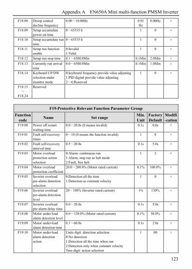
Appendix A EN650A Mini multi-function PMSM Inverter
123
F18.08 Droop control decline frequency
0.00~10.00Hz 0.01 Hz
0.00Hz
F18.09 Setup accumulate power on time
0~65535 h 1 0
F18.10 Setup accumulate run time
0~65535 h 1 0
F18.11 Setup run function enable
0:Invalid 1:Valid
1 0
F18.12 Setup run stop time 0.1~6500.0Min 0.1Min 2.0Min
F18.13 Currently run arrival time
0.0~6500.0Min 0.1Min 1.0Min
F18.14 Keyboard UP/DW selection under monitor mode
0:keyboard frequency provide value adjusting 1:PID digital provide value adjusting 2~6:Reserved
1 0
F18.15 ~
F18.24
Reserved
F19-Protective Relevant Function Parameter Group
Function code
Name Set range Min. Unit
FactoryDefault
Modifi-cation
F19.00 Power off restart waiting time
0.0~20.0s (0 means invalid) 0.1s 0.0s ×
F19.01 Fault self-recovery times
0~10 (0 means the function invalid) 1 0 ×
F19.02 Fault self-recovery interval time
0.5~20.0s 0.1s 5.0s ×
F19.03 Motor overload protection action selection
0:Alarm: continuous run 1:Alarm, stop run as halt mode 2:Fault, free halt
1 2 ×
F19.04 Motor overload protection coefficient
20.0~200.0% (Motor rated current) 0.1% 100.0% ×
F19.05 Inverter overload pre-alarm detection selection
0:Detection all the time 1:Detection as constant velocity
1 0 ×
F19.06 Inverter overload pre-alarm detection level
20~180% (Inverter rated current)
1% 130%
F19.07 Inverter overload pre-alarm delay time
0.0~20.0s 0.1s 5.0s
F19.08 Motor under-load alarm detection level
0.0~120.0% (Motor rated current) 0.1% 50.0%
F19.09 Motor under-load alarm detection time
0.1~60.0s 0.1s 2.0s
F19.10 Motor under-load alarm detection action
Units digit: detection selection 0:No detection 1:Detection all the time when run 2:Detection only when constant velocity Tens digit: action selection
1 00

Appendix A EN650A Mini multi-function PMSM Inverter
124
0:Alarm, continuous run 1:Alarm, stop run as halt mode 2:Fault, free halt
F19.11 Input& output phase loss, short circuit detection action
Units digit: input phase loss 0:No detection 1:Fault, free halt Tens digit: output phase loss 0:No detection 1:Fault, free halt Hundreds digit: power-on on earth short circuit protect detection enable 0:No detection 1:Fault, free halt Thousands digit: operation on earth short circuit protect detection enable 0:No detection 1:Fault, free halt
1 1100
F19.12 Over voltage stall selection
0:Forbid 1:Allowed
1 1 ×
F19.13 Over voltage stall protection voltage
120~150% (Rated DC bus voltage) 1% 125% ×
F19.14 Automatic current limit level
110~200% 1% 150% ×
F19.15 Frequency decline rate of automatic current limit
0.00~99.99Hz/s 0.01 Hz/s
10.00 Hz/s
×
F19.16 Automatic current limit action selection
0:Constant velocity invalid 1:Constant velocity valid
1 0 ×
F19.17 Reserved F19.18 Motor run section
selection when instant power off
0:Forbid 1:Allowed
1 0 ×
F19.19 Frequency droop rate when instant power off
0.00~99.99Hz/s 0.01 Hz/s
10.00 Hz/s
×
F19.20 Voltage rebound estimate time when instant power off
0.00~10.00s 0.01s 0.10s ×
F19.21 Action estimate voltage when instant power off
60~100%(Rated DC bus voltage) 1% 80% ×
F19.22 Allowed the longest off time when instant power off
0.30~5.00s 0.01s 2.00s ×
F19.23 Terminal external device fault action selection
0:Alarm, continuous run 1:Alarm, stop run as halt mode 2:Fault, free halt
1 2 ×
F19.24 Power on terminal protection selection
0:Invalid 1:Valid
1 1 ×
F19.25 Provide lost detection value
0~100% 1% 0%

Appendix A EN650A Mini multi-function PMSM Inverter
125
F19.26 Provide lost detection time
0.0~20.0s 0.1s 0.5s
F19.27 Feedback lost detection value
0~100% 1% 12%
F19.28 Feedback lost detection time
0.0~20.0s 0.1s 0.5s
F19.29 Deviation magnitude abnormal detection value
0~100% 1% 50%
F19.30 Deviation magnitude abnormal detection time
0.0~20.0s 0.1s 0.5s
F19.31 Protection action selection 1
Units digit: PID provide loss detection act 0:No detection 1:Alarm, continue run 2:Alarm, stop run as halt mode 3:Fault, free halt Tens digit: PID feedback loss detection act 0:No detection 1:Alarm, continue run 2:Alarm, stop run as halt mode 3:Fault, free halt Hundreds digit: PID error value abnormal detect action 0:No detection 1:Alarm, continue run 2:Alarm, stop run as halt mode 3:Fault, free halt
1 000
F19.32 Protection action selection 2
Units digit: Communication abnormal action: include communication time out and error 0:Alarm, continue run 1:Alarm, stop run as halt mode 2:Fault, free halt Tens digit: E2PROM abnormal action selection0:Alarm, continue run 1:Alarm, stop run as halt mode 2:Fault, free halt Hundreds digit: Contactor abnormal action 0:Alarm, continue run 1:Alarm, stop run as halt mode 2:Fault, free halt Thousands digit: under-voltage fault indication action selection 0:No detection 1:Fault, free halt
1 1200 ×
F19.33 Over-speed protection selection
0:Invalid 1:Valid
1 0 ×
F19.34 Over-speed protection threshold level
0.00~400.00Hz 0.01Hz 60.00Hz ×

Appendix A EN650A Mini multi-function PMSM Inverter
126
F19.35 Fault indication and clock during the period of recovery
Units digit: Fault indication selection during the period of fault reset automatically 0:Action 1:No action Tens digit: Fault clock function selection, to achieve fault display before power down etc. 0:Forbid 1:Open
1 00 ×
F19.36 Continuous run frequency selection when alarm
Match up with protect action 0:Run at the frequency setup by now 1:Run at the frequency of upper limit 2:Run at the frequency of low limit 3:Run at the frequency of abnormal for standby
1 0 ×
F19.37 Abnormal standby frequency
0.00Hz~Upper limit Fre. 0.01Hz 10.00Hz ×
F19.38 ~
F19.44
Reserved
F20-Internal Virtual Input Output Node Parameter Group
Function
code Name Set range
Min.
Unit
Factory
Default
Modifi
-cationF20.00 Virtual input VDI1
function selection 0~90 1 0
F20.01 Virtual input VDI2 function selection
0~90 1 0
F20.02 Virtual input VDI3 function selection
0~90 1 0
F20.03 Virtual input VDI4 function selection
0~90 1 0
F20.04 Virtual input VDI5 function selection
0~90 1 0
F20.05 Virtual output VDO1 function selection
0~60 1 0
F20.06 Virtual output VDO2 function selection
0~60 1 0
F20.07 Virtual output VDO3 function selection
0~60 1 0
F20.08 Virtual output VDO4 function selection
0~60 1 0
F20.09 Virtual output VDO5 function selection
0~60 1 0
F20.10 Virtual output VDO1 open delay time
0.00~600.00s 0.01s 0.00s
F20.11 Virtual output VDO2 open delay time
0.00~600.00s 0.01s 0.00s
F20.12 Virtual output VDO3 open delay time
0.00~600.00s 0.01s 0.00s

Appendix A EN650A Mini multi-function PMSM Inverter
127
F20.13 Virtual output VDO4 open delay time
0.00~600.00s 0.01s 0.00s
F20.14 Virtual output VDO5 open delay time
0.00~600.00s 0.01s 0.00s
F20.15 Virtual output VDO1 close delay time
0.00~600.00s 0.01s 0.00s
F20.16 Virtual output VDO2 close delay time
0.00~600.00s 0.01s 0.00s
F20.17 Virtual output VDO3 close delay time
0.00~600.00s 0.01s 0.00s
F20.18 Virtual output VDO4 close delay time
0.00~600.00s 0.01s 0.00s
F20.19 Virtual output VDO5 close delay time
0.00~600.00s 0.01s 0.00s
F20.20 Virtual input VDI enable control
00~FF 1 00
F20.21 Virtual input VDI status digital setup
00~FF 1 00
F20.22 Virtual input/output connection
00~FF Bit0:VDI1 and VDO1 connection 0:Positive logic 1:Negative logic Bit1:VDI2 and VDO2 connection 0:Positive logic 1:Negative logic Bit3:VDI3 and VDO3 connection 0:Positive logic 1:Negative logic Bit4:VDI4 and VDO4 connection 0:Positive logic 1:Negative logic Bit4:VDI5 and VDO5connection 0:Positive logic 1:Negative logic
1 00
F21-Reserved parameters group 3
Function code
Name Set range Min. Unit
FactoryDefault
Modifi-cation
F21.00 ~
F21.21
Reserved
F22-Reserved parameters group 4
Function code
Name Set range Min. Unit
FactoryDefault
Modifi-cation
F22.00 ~
F22.17
Reserved

Appendix A EN650A Mini multi-function PMSM Inverter
128
F23-Reserved parameters group 5
Function code
Name Set range Min. Unit
FactoryDefault
Modifi-cation
F23.00 ~
F23.17
Reserved
F24-Reserved parameters group 6
Function code
Name Set range Min. Unit
FactoryDefault
Modifi-cation
F24.00 ~
F24.13
Reserved
F25-User Definition Display Parameter Group
Function code
Name Set range Min. Unit
FactoryDefault
Modifi-cation
F25.00 User Function Code 1 F00.00~F25.xx 0.01 25.00 F25.01 User Function Code 2 F00.00~F25.xx 0.01 25.00 F25.02 User Function Code 3 F00.00~F25.xx 0.01 25.00 F25.03 User Function Code 4 F00.00~F25.xx 0.01 25.00 F25.04 User Function Code 5 F00.00~F25.xx 0.01 25.00 F25.05 User Function Code 6 F00.00~F25.xx 0.01 25.00 F25.06 User Function Code 7 F00.00~F25.xx 0.01 25.00 F25.07 User Function Code 8 F00.00~F25.xx 0.01 25.00 F25.08 User Function Code 9 F00.00~F25.xx 0.01 25.00 F25.09 User Function Code 10 F00.00~F25.xx 0.01 25.00 F25.10 User Function Code 11 F00.00~F25.xx 0.01 25.00 F25.11 User Function Code 12 F00.00~F25.xx 0.01 25.00 F25.12 User Function Code 13 F00.00~F25.xx 0.01 25.00 F25.13 User Function Code 14 F00.00~F25.xx 0.01 25.00 F25.14 User Function Code 15 F00.00~F25.xx 0.01 25.00 F25.15 User Function Code 16 F00.00~F25.xx 0.01 25.00 F25.16 User Function Code 17 F00.00~F25.xx 0.01 25.00 F25.17 User Function Code 18 F00.00~F25.xx 0.01 25.00 F25.18 User Function Code 19 F00.00~F25.xx 0.01 25.00 F25.19 User Function Code 20 F00.00~F25.xx 0.01 25.00 F25.20 User Function Code 21 F00.00~F25.xx 0.01 25.00 F25.21 User Function Code 22 F00.00~F25.xx 0.01 25.00 F25.22 User Function Code 23 F00.00~F25.xx 0.01 25.00 F25.23 User Function Code 24 F00.00~F25.xx 0.01 25.00 F25.24 User Function Code 25 F00.00~F25.xx 0.01 25.00 F25.25 User Function Code 26 F00.00~F25.xx 0.01 25.00 F25.26 User Function Code 27 F00.00~F25.xx 0.01 25.00

Appendix A EN650A Mini multi-function PMSM Inverter
129
F25.27 User Function Code 28 F00.00~F25.xx 0.01 25.00 F25.28 User Function Code 29 F00.00~F25.xx 0.01 25.00 F25.29 User Function Code 30 F00.00~F25.xx 0.01 25.00
F26-Fault Record Function Parameter Group
Function code
Name Set range Min. Unit
FactoryDefault
Modifi-cation
F26.00 The last fault record 0:No fault 1:Overcurrent at acceleration 2:Overcurrent at deceleration 3:Overcurrent at constant speed 4:Overvoltage at acceleration 5:Overvoltage at deceleration 6:Overvoltage at constant speed 7:Overvoltage at motor halt 8:Undervoltage at run 9:Drive overload protection 10:Motor overload protection 11:Motor under-load protection 12:Input phase loss 13:Output phase loss 14:Inverter module protection 15:Short circuit to earth at run 16:Short circuit to earth when power on 17:Drive overheat 18:Rxternal device fault 19:Current detect circuit fault 20:External interference 21:Internal interference—main clock etc 22:PID provide lost 23:PID feedback lost 24:PID error value abnormal 25:Terminal protection activate 26:Communication fault 27~29:reserved 30:EEROM read-write error 31:Temperature detection disconnection 32:Auto-tunning fault 33:Contactor abnormal 34:Factory fault 1 35:Factory fault 2 36:Capacitor overheat(few mode with overheat protection) 37:Encoder disconnection 38:Over-speed protection 39~50:Reserved
1 0 *
F26.01 The last two fault records
Same as above 1 0 *
F26.02 The last three fault records
Same as above 1 0 *

Appendix A EN650A Mini multi-function PMSM Inverter
130
F26.03 The last four fault records
Same as above 1 0 *
F26.04 Setup frequency at the last one fault
0.00Hz~Upper limit Fre. 0.01 Hz
0.00 Hz
*
F26.05 Output frequency at the last one fault
0.00Hz~Upper limit Fre. 0.01 Hz
0.00 Hz
*
F26.06 Output current at the last one fault
0.0~6553.5A 0.1A 0.0A *
F26.07 DC bus voltage at the last one fault
0.0~6553.5V 0.1V 0.0V *
F26.08 Module temperature at the last one fault
0~125 1 0 *
F26.09 Input terminal status at the last one fault
0 *
F26.10 Accumulated run time at the last one fault
0~65535min 1min 0min *
F26.11 Setup frequency at the last two fault
0.00Hz~Upper limit Fre. 0.01 Hz
0.00 Hz
*
F26.12 Output frequency at the last two fault
0.00Hz~Upper limit Fre. 0.01 Hz
0.00 Hz
*
F26.13 Output current at the last two fault
0.0~6553.5A 0.1A 0.0A *
F26.14 DC bus voltage at the last two fault
0.0~6553.5V 0.1V 0.0V *
F26.15 Module temperature at the last two fault
0~125 1 0 *
F26.16 Input terminal status at the last two fault
0 *
F26.17 Accumulated run time at the last two fault
0~65535h 1h 0h *
F24-Reserved parameters group 6
Function code
Name Set range Min. Unit
FactoryDefault
Modifi-cation
F27.00 User password 00000~65535 1 00000 F27.01 Manufacturer password 00000~65535 1 00000
C-Monitor Function Parameter Group
Function Code
Name Min. Unit
FactoryDefault
Modifi-cation
C-00 Display the parameter of F00.01、F00.07 definition
C-01 Display the parameter of F00.02、F00.08 definition
C-02 Display the parameter of F00.03、F00.09 definition

Appendix A EN650A Mini multi-function PMSM Inverter
131
C-03 Display the parameter of F00.04、F00.10 definition
C-04 Display the parameter of F00.05、F00.11 definition
C-05 Display the parameter of F00.06、F00.12 definition
Appendix B Free-port Communication Protocol
132
Appendix B Free-port Communication Protocol
B.1 Summarization We provide the customer with general RS485/RS232 communication interface
in our EN630 series frequency inverter. For the users, through the communication interface upper device (such as PC, PLC controller etc.) can perform centralized monitor to the inverter (such as setting inverter parameter, controlling run of inverter, reading work state of the inverter) and also long-distance control keypad can be connected to realize diverse operating requirement of the user.
This communication protocol is interface criterion file designed for realizing above-mentioned function, please read it earnestly and program according to it so that realize long-distance and network control to the inverter.
B.2 Protocol content and description
B.2.1 Communication net buildup mode
B.2.2 Communication mode
At present, EN630 inverter can be used as not only auxiliary device but also mainframe device in RS485, if the inverter is used as auxiliary device, master device can be completed by PC, PLC or human interface, and if used as mainframe device, the main-auxiliary control of the inverter can be complement by it, Specific communication mode is as mentioned below:
(1) PC or PLC as mainframe, inverter as auxiliary device, point-to-point
232-485 conversion module
RS485
EN630 mainframeMainframe is PC Mainframe is PLC
RS232
Or Or
EN630 EN630
EN630 EN630
……

Appendix B Free-port Communication Protocol
133
communication between mainframe and auxiliary device. (2) Auxiliary device don’t response when mainframe send out command by
broadcast address. (3) User can set local address, baud rate and data format of the inverter through
auxiliary device keypad. (4) Auxiliary device report current failure information to mainframe in the last
response frame. (5) EN630 provides RS485 interface.
B.2.3 Transport mode Asynchronous serial, half-duplex transmission mode. Default format and
transport rate: 8-N-1, 9600bps.For specific parameter setting please see description for F05 group function code.
(Remark: The definition for this parameter is only effective under free – port communication mode, and definition for other parameters are the same as original)
F05.00 Protocol selection
0:Modbus protocol 1:Reserved 2:Profibus protocol(Extension effective) 3:CanLink protocol(Extension effective) 4:CANopen protocol(Extension effective) 5:Freedom protocol 1(Can modify all function parameters of EN500/EN600) 6:Freedom protocol 2 (Can only modify part of function parameter of EN500/EN600) Remark: Expansion card is needed if select protocol 2, 3, 4
1 0 ×
F05.01 Baud rate configuration
LED first bit: free protocol and Modbus baud rate selection 0:300BPS 1:600BPS 2:1200BPS 3:2400BPS 4:4800BPS 5:9600BPS 6:19200BPS 7:38400BPS 8:57600BPS
1 005 ×
F05.02 Data format
LED first bit: Freedom protocol and Modbus protocol data format 0:1-8-1 format, no checkout, RTU 1:1-8-1 format, even checkout, RTU 2:1-8-1 format, odd checkout, RTU 3:1-7-1 format, no checkout, ASCII
00 ×

Appendix B Free-port Communication Protocol
134
4:1-7-1 format, even checkout, ASCII 5:1-7-1 format, odd checkout, ASCII
F05.03 Local address 0~247, 00 is master station address 1 1 ×
B.2.4 Data command frame format
Main device command frame format
Sending order
1 2 3 4 5 6 7 8 9 10 11 12 13 14 15 16 17 18
frame h
ead
auxiliary d
evice add
ress
auxiliary d
evice add
ress
main
device com
man
d
main
device com
man
d
assistant in
dex
assistant in
dex
comm
and
ind
ex
comm
and
ind
ex
set data
set data
set data
set data
check
out su
m
check
out su
m
check
out su
m
check
out su
m
frame en
d
Defin
ition
head
add
ress
Com
man
d area
Ind
ex area
Settin
g data area
check
out area
end
Sending byte
1 2 2 4 4 4 1
Main device command frame format
Sending order
1 2 3 4 5 6 7 8 9 10 11 12 13 14 15 16 17 18

Appendix B Free-port Communication Protocol
135
frame h
ead
auxiliary d
evice add
ress
auxiliary d
evice add
ress
auxiliary d
evice respon
se
auxiliary d
evice respon
se
failure in
dex
failure in
dex
comm
and
ind
ex
comm
and
ind
ex
run
data
run
data
run
data
run
data
check
out su
m
check
out su
m
check
out su
m
check
out su
m
frame en
d
Defin
ition
head
add
ress
respon
se
area
Ind
ex area
Ru
n d
ata area
Ch
eckou
t area
end
Sending byte
1 2 2 4 4 4 1
Fig.B-2 Command/Response frame format Remark:
(1) “Setting data area” and “run data area” may not be existent in some command/data frame format, so in protocol command list it’s marked with “nothing”.
(2) In protocol effective character set is: ~,1, 2, 3, 4, 5, 6, 7, 8, 9, A, B, C, D, E,F and hex data 0DH, ASCII lowercase a, b, c, d, e, f are invalid.
(3) Effective command frame length is 14 or 18 byte.
B.2.5 Explanation and description for format (1) Frame head
It’s character“~” (namely hex 7E), single byte. (2) Auxiliary device address
Data meanings: local address of auxiliary device, double byte. ASCII format. Inverter factory default is 01. (3) Mainframe command/auxiliary device respond
Data meanings: mainframe send out command and auxiliary device respond to the command. Double byte, ASCII format.
Response code function classification: Species 1>: Command code=“10”, mainframe ask auxiliary device to report
current preparation state and control situation.

Appendix B Free-port Communication Protocol
136
Table B-1 Command code meanings for response frame response area
Response code
ASCII
Meanings
Preparation state of auxiliary device
Control from mainframe is allowed
To set frequency is allowed
10 Haven’t get ready No meaning
11 Get ready Allow Allow
12 Get ready Allow Allow
13 Get ready Don’t allow Don’t allow
14 Get ready Don’t allow Don’t allow
20 Frame error
Species 2>: Command code=“11”~“15”, 5 kinds of function command which mainframe send to auxiliary device, For detail please see protocol command list.
Table B-2 Response code meanings for response frame command index area
Response code
ASCII Meanings of response code description
00
Auxiliary device communication
and control is normal; function
code modification is effective;
password is correct.
20
(1) Frame checkout error;
(2)“Command area” data overrun;(3)“Index area” data overrun;
(4) Frame length error/non ASCII
byte exist in area except frame
head, frame end.
When this response code is
reported, data of “command area”,
“index area” and “running data
area” are not reported.
30
(1) Control to auxiliary device is
ineffective;
(2) Ineffective function code
parameter modification;
(3)“Setting/Running data” area data
overrun.
(4) Password error.
Whether report this response code
relate to current set state of
auxiliary device. When report data
of area”, “index area” and “run data
area” are reported according to
protocol requirement.
(4) Auxiliary index/command index/failure index Data meanings: Include auxiliary index byte and command index byte. For mainframe, Auxiliary index, command index are used for cooperating
mainframe command in realizing specific function.

Appendix B Free-port Communication Protocol
137
For auxiliary device, auxiliary index, command index are used for reporting failure state code, command index are reported without modification
Data type: hex, 4 byte, ASCII format. Command index occupy 2 low byte, data range: “00”~“FF”. Auxiliary index occupy 2 high byte, data range: “00”~“FF”. Auxiliary device failure state occupy “auxiliary index’’ byte, see table B-3.
Table B-3 Free-port1 failure type description
Failure code
(Decimal) Description
Failure code
(Decimal) Description
1 Overcurrent during accelerating process
19 Current detecting circuit failure
2 Overcurrent during decelerating process
20 External interference failure
3 Overcurrent during constant speed process
21 Internal interference failure
4 Overvoltage during accelerating process
22 PID provision loss
5 Overvoltage during decelerating process
23 PID feedback loss
6 Overvoltage during constant speed process
24 PID error amount exception
7 Overvoltage while halting 25 Startup terminal protection
8 Under voltage during running process
26 RS485 communication failure
9 Inverter overload protection
27 Reserved
10 Motor overload protection 28 Reserved
11 Motor underload protection
29 Reserved
12 Input phase missing 30 E2PROM read and write wrongly
13 Output phase missing 31 Temperature detection breakage
14 Inverting module protection
32 Self-tuning failure
15 Short circuit to earth during running process
33 Contactor exception
16 Short circuit to earth during electrifying process
34 Interior failure 1
17 Inverter over heating

Appendix B Free-port Communication Protocol
138
18 External device failure
Free-port 2 Failure type description
Failure code
(decimal) Description
Failure code
(decimal) Description
1 Overcurrent during accelerating process
13 Inverting module protection
2 Overcurrent during decelerating process
14 External device failure
3 Overcurrent during constant speed process
15 Current detecting circuit failure
4 Overvoltage during accelerating process
16 RS485 communication failure
5 Overvoltage during decelerating process
17 Reserved
6 Overvoltage during constant speed process
18 Reserved
7 Control power supply overvoltage
19 Under voltage
8 Inverter overload 20 System interference
9 Motor overload 21 Reserved
10 Inverter over heating 22 Reserved
11 Reserved 23 E2PROM read and write wrongly
12 Reserved
(5) Checkout sum Data meanings: frame checkout, 4 byte, ASCII. Calculation method: accumulative sum of ASCII code value of all byte from
“auxiliary device address ”to“ run data”. (6) Frame end
Hex 0D, single byte.
B.2.6 Protocol command list
Frame 7E and frame end 0D, address, checkout sum, ASCII character format are omitted in following description.
Table B-4 Free-port 1 protocol command table

Appendix B Free-port Communication Protocol
139
Nam
e
Main
frame ord
er D
ecimal
Au
xiliary ind
ex Hex
Ord
er ind
ex H
ex
Ru
n d
ata setting ran
ge H
ex
Main
frame sen
din
g exam
ple, su
ch as P
C
control op
eration of
inverter
(C lan
guage clu
ster form
at , auxiliary d
evice is set to 01)
Ru
n d
ata precision
Descrip
tion
Look up auxiliary motor state
10 00 00 no ~010A00000192\r 1
Read
param
et- er of au
xiliary motor
Main setting frequency
11 00 00 no ~010B00000193\r 0.01 Hz
Auxiliary setting
frequency 11 00 01 no ~010B00010194\r
0.01 Hz
Setting frequency
11 00 02 no ~010B00020195\r 0.01 Hz
Output frequency
11 00 03 no ~010B00030196\r 0.01 Hz
Output current 11 00 04 no ~010B00040197\r 0.1A Output voltage
11 00 05 no ~010B00050198\r 1V
DC bus-bar voltage
11 00 06 no ~010B00060199\r 0.1V
Load motor revolving
speed 11 00 07 no ~010B0007019A\r
1RPM
Load motor linear speed
11 00 08 no ~010B0008019B\r no
Inverter temperature
11 00 09 no ~010B0009019C\r 1
Runtime 11 00 0A no ~010B000A01A4\r 0.1 min
Current accumulative
runtime 11 00 0B no ~010B000B01A5\r 1H
Current accumulative
power-on time 11 00 0C no ~010B000C01A6\r 1H
Inverter state 11 00 0D no ~010B000D01A7\r No Input terminal 11 00 0E no ~010B000E01A8\r No

Appendix B Free-port Communication Protocol
140
state Output
terminal state 11 00 0F no ~010B000F01A9\r No
Expand output terminal state
11 00 10 no ~010B00100194\r No
Expanding input terminal
state 11 00 11 no ~010B000F0195\r No
Communicational virtual
input terminal state
11 00 12 no ~010B000F0196\r No
Internal virtual input node state
11 00 13 no ~010B000F0197\r No
Analog input AI1
11 00 14 no ~010B000F0198\r No
Analog input AI2
11 00 15 no ~010B000F0199\r No
Expanding analog input
EAI1 11 00 16 no ~010B000F019A\r No
Expanding analog input
EAI2 11 00 17 no ~010B000F019B\r No
Analog AO1 output
11 00 18 no ~010B000F019C\r No
Analog AO2 output
11 00 19 no ~010B000F019D\r No
Expanding analog EAO1
output 11 00 1A no ~010B000F01A5\r No
Expanding analog EAO2
output 11 00 1B no ~010B000F01A6\r No
External pulse input
frequency 11 00 1C no ~010B000F01A7\r 1Hz
Operational panel
potentiometer voltage
11 00 1D no ~010B000F01A8\r 0.01
V
Process PID provision
11 00 1E no ~010B000F01A9\r 0.01
V

Appendix B Free-port Communication Protocol
141
Process PID feedback
11 00 1F no ~010B000F01AA\r 0.01
V
Process PID error
11 00 20 no ~010B000F0195\r 0.01
V
Process PID output
11 00 21 no ~010B000F0196\r 0.01Hz
Simple PLC current
segments 11 00 22 no ~010B000F0197\r No
External multi-section speed current
segments
11 00 23 no ~010B000F0198\r No
Provision pressure for
constant pressure water
11 00 24 no ~010B000F0199\r 0.001 Mpa
Feedback pressure for
constant pressure water
11 00 25 no ~010B000F019A\r 0.001 Mpa
Relay state for constant
pressure water 11 00 26 no ~010B000F019B\r No
Current length 11 00 27 no ~010B000F019C\r No Accumulative
length 11 00 28 no ~010B000F019D\r No
Current internal count
11 00 29 no ~010B000F019E\r No
Current internal time
11 00 2A no ~010B000F01A6\r No
Setting channel for
run command 11 00 2B no ~010B000F01A7\r No
Main frequency provision channel
11 00 2C no ~010B000F01A8\r No
Auxiliary frequency provision channel
11 00 2D no ~010B000F01A9\r No
Inverter rated current
11 00 2E no ~010B000F01AA\r 0.1A

Appendix B Free-port Communication Protocol
142
Inverter rated voltage
11 00 2F no ~010B000F01AB\r 1V
Inverter rated power
11 00 30 no ~010B000F0196\r 0.1 KW
Reserved Reserved Frequency
after acceleration
and deceleration
11 00 33 no ~010B00330199\r 0.01Hz
Motor rotor frequency
11 00 34 no ~010B0034019A\r 0.01Hz
Current provision
torque 11 00 35 no ~010B0035019B\r 0.1%
Current output torque
11 00 36 no ~010B0036019C\r 0.1%
Current torque current
11 00 37 no ~010B0037019D\r 0.1A
Current flux current
11 00 38 no ~010B0038019E\r 0.1A
Auxiliary device run command
12 00 00 no ~010C00000194\r No
Set current run frequency provision of auxiliary device
12 00 01
0Hz~high limit freq
~010C00010FA0027C\r
0.01Hz
Set freq.=40.00Hz
Run control and adjusting function
Auxiliary device run with run frequency provision
12 00 02
0Hz~high limit freq
~010C00020FA0027D\r
0.01Hz
Auxiliary device run Set freq.=40.00Hz
Auxiliary device forward run
12 00 03 no ~010C00030197\r No
Auxiliary device reverse run
12 00 04 no ~010C00040198\r No
Auxiliary 12 00 05 0Hz~ ~010C00050FA00 0.01 Forward

Appendix B Free-port Communication Protocol
143
device forward run with run frequency provision
high limit freq
280\r Hz run boot-strap Set freq.=40.00Hz
Auxiliary device reverse run with run frequency provision
12 00 06
0Hz~ high limit freq
~010C00060FA00281\r
0.01Hz
Reverse run boot-strap Set freq.=40.00Hz
Auxiliary device stop
12 00 07 no ~010C0007019B\r No
Auxiliary device jog run
12 00 08 no ~010C0008019C\r No
Auxiliary device forward jog run
12 00 09 no ~010C0009019D\r No
Auxiliary device reverse jog run
12 00 0A no ~010C000A01A5\r No
Auxiliary device stop run
12 00 0B no ~010C000B01A6\r No
Auxiliary device failure restoration
12 00 0C no ~010C000C01A7\r No S
oftware
version q
uery
order
Query auxiliary device software version
15 00 00 no ~010F00000197\r 1
Free-Port 2 protocol command table

Appendix B Free-port Communication Protocol
144
Nam
e
Main
frame ord
er D
ecimal
Au
xiliary In
dex H
ex
Ord
er ind
ex Hex
Ru
n d
ata setting ran
ge H
ex
Main
frame sen
din
g exam
ple, su
ch asP
C
control op
eration of
inverter (C
langu
age clu
ster format , au
xiliary d
evice is set to 01)
Ru
n d
ata precision
Descrip
tion
Look up auxiliary motor state 10 00 00 no ~010A00000192\r 1
Run control
and adjusting function
Auxiliary device run command
12 00 00 no ~010C00000194\r no
Set current run freq. of auxiliary device
12 00 01 0Hz~ high limit freq
~010C00010FA0027C\r 0.01Hz
Auxiliary device run with run frequency provision
12 00 02 0Hz~ high limit freq
~010C00020FA0027D\r 0.01Hz
Auxiliary device forward run
12 00 03 no ~010C00030197\r no
Auxiliary device reverse run
12 00 04 no ~010C00040198\r no
Auxiliary device forward run with run frequency provision
12 00 05 0Hz~ high limit freq
~010C00050FA00280\r 0.01Hz
Auxiliary device reverse run with run frequency provision
12 00 06 0Hz~ high limit freq
~010C00060FA00281\r 0.01Hz
Auxiliary device stop 12 00 07 no ~010C0007019B\
r no
Auxiliary device jog run
12 00 08 no ~010C0008019C\r no
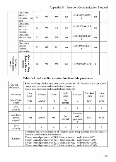
Appendix B Free-port Communication Protocol
145
Auxiliary device forward jog run
12 00 09 no ~010C0009019D\r no
Auxiliary device reverse jog run
12 00 0A no ~010C000A01A5\r no
Auxiliary device stop run
12 00 0B no ~010C000B01A6\r no
Auxiliary device failure restoration
12 00 0C no ~010C000C01A7\r no
Softw
are version
qu
ery ord
er
Qu
ery auxiliary
device softw
are version
15 00 00 no ~010F00000197\r 1
Table B-5 read auxiliary device function code parameter
Function definition
Read auxiliary device function code parameter: all function code parameter except user password and manufacturer password except user password and manufacturer password
Meanings Frame head Address Order Order
index Run data Checkout sum
Frame end
Mainframe order 7EH ADDR 13 See
remark 4 BCC 0DH
Byte quantity 1 2 2 4 0 4 1
Auxiliary device
respond 7EH ADDR 06 See
remark
Function code
parameter
BCC 0DH
Byte quantity 1 2 2 4 4 4 1
Remark
Command index=combination of function code group number and hex code of function code number. For instance: If want to read parameter of F0.05 function code, order index=0005; If want to read parameter of F2.11 function code, order index =020B; If want to read parameter of F2.15 function code, order index =020F; If want to read parameter of F2.13 function code, order index =020D;

Appendix B Free-port Communication Protocol
146
Corresponding relation between decimal and hex value of function code group No.
Function code group
No Decimal Hex
Function code group
No Decimal Hex
F00 0 00H F0E 14 0EH
F01 1 01H F0F 15 0FH
F02 2 02H F10 16 10H
F03 3 03H F11 17 11H
F04 4 04H F12 18 12H
F05 5 05H F13 19 13H
F06 6 06H F14 20 14H
F07 7 07H F15 21 15H
F08 8 08H F16 22 16H
F09 9 09H F17 23 17H
F0A 10 0AH F18 24 18H
F0B 11 0BH F19 25 19H
F0C 12 0CH F1A 26 1AH
F0D 13 0DH F1B 27 1BH
Virtual data 0~FFFF (namely 0~65535)
Please input correct “user password” before you set user function code parameter.
Table B-6 set auxiliary device function code parameter
Function definition
Set auxiliary device function code parameter: all function code parameter except user password and manufacturer password
Meanings Frame head Address Order Order
index Run data Checkout sum Frame end
Mainframe order 7EH ADDR 14 See
remark 4 BCC 0DH
Byte quantity 1 2 2 4 0 4 1
Auxiliary device
respond 7EH ADDR 06 See
remark
Function code
parameter
BCC 0DH
Byte quantity 1 2 2 4 4 4 1

Appendix B Free-port Communication Protocol
147
Remark
Command index=combination of function code group number and hex code of function code number. For instance: If want to read parameter of F00.05 function code, order index=0005; If want to read parameter of F02.11 function code, order index =020B; If want to read parameter of F02.15 function code, order index =020F; If want to read parameter of F02.13 function code, order index =020D;
Corresponding relation between decimal and hex value of function code group No.
Function code
group No Decimal Hex
Function code
group NoDecimal Hex
F00 0 00H F0E 14 0EH
F01 1 01H F0F 15 0FH
F02 2 02H F10 16 10H
F03 3 03H F11 17 11H
F04 4 04H F12 18 12H
F05 5 05H F13 19 13H
F06 6 06H F14 20 14H
F07 7 07H F15 21 15H
F08 8 08H F16 22 16H
F09 9 09H F17 23 17H
F0A 10 0AH F18 24 18H
F0B 11 0BH F19 25 19H
F0C 12 0CH F1A 26 1AH
F0D 13 0DH F1B 27 1BH
Virtual data 0~FFFF(namely 0~65535)

Appendix C Modbus communication protocol
148
Appendix C Modbus communication protocol
C.1 Summary We provide general RS485 communication interface in our EN630/ EN650A
inverters for the user. Through this communication interface upper device (such as HMI, PC, PLC controller and etc.) can perform centralized monitor to the inverter (Such as to set inverter parameter, control run of inverter, read work state of the inverter).
This communication protocol is interface criterion file designed for realizing above-mentioned function, please read it earnestly and program according to it so that realize long-distance and network control to the inverter.
C.2 Communication net buildup mode
Fig.C-1 Net buildup graph
C.3 Communication mode At present, EN630/EN650A inverter can be used only as Slave device in RS485
net. Can realize communication between inverters through PC, PLC or HMI if it’s needed. Specific communication mode is as mentioned below:
(1) PC or PLC as mainframe, inverter as Slave device, point-to-point communication between mainframe and Slave device.
(2) Slave device don’t response when mainframe send out command by broadcast address.
Mainframe is PC Mainframe is PLC
232-485 conversionmodule
EN630 EN630 EN650A EN650A
or
RS232
RS485

Appendix C Modbus communication protocol
149
(3) User can set local address, baud rate and data format of the inverter through (4) Slave device keypad or serial communication mode. (5) EN630/ EN650A provides the RS485 interface. (6) Default mode: Asynchronous serial,semiduplex transport mode. There are
RTU and ASII two mode . Default format and transport rate: 8-N-1, 9600bps.
C.4 Transmission mode Asynchronous serial, semiduplex transport mode. Default format and transport
rate: 8-N-1, 9600bps. The detail setting parameter, please refer to the F05 group function mode.
(Remark: The parameter is valid under the Modbus communication, the other parameter comply with the original service manual)
F05.00 Protocol selection
0:Modbus protocol 1:Reserved 2:Reserved 3:Reserved 4:Reserved 5:Free protocol 1(revision all the parameter of EN630/EN650A is valid) 6: Free protocol 2(only revising part parameter of EN630/EN650A is valid)
1 0 ×
F05.01 Baud rate setting
LED the unit digital: free protocol and Modbus Baud rate selection 0:300BPS 1:600BPS 2:1200BPS 3:2400BPS 4:4800BPS 5:9600BPS 6:19200BPS 7:38400BPS 8:57600BPS
1 005 ×
F05.02 Data format LED the unit digital: free protocol and Modbus protocol Data format 0:1-8-1 format,no checkout,RTU 1:1-8-1 format,Odd Parity,RTU 2:1-8-1 format,Even Parity,RTU 3:1-7-1 format,no checkout,ASCII 4:1-7-1 format,Odd Parity,ASCII 5:1-7-1 format,Even Parity,ASCII
00 ×
F05.03 Local address
0~247,00 is broadcast address 1 1 ×

Appendix C Modbus communication protocol
150
C.5 Data communication structure
C.5.1 Data frame format Using RTU mode, messages are sent at least 3.5 character time interval pause.
The first transmitted field is device address, the character you can transfer is hexadecimal 0x00 ~ 0xFF. Network equipment Continuously monitor the bus, including pauses. When the address field is received, all equipment determine whether it is sent to their own. when the last character of the packet transfer is complete, at least a 3.5 character times pause mean the end of the message. A new
Message can begin after this pause.The entire message frame must be transmitted as a continuous flow. If a new message start transmitting in less than 3.5 character times after a message and then receiving device will consider it a continuation of the previous message. This will cause an error, because in the final CRC field value can not be right.
RTU frame format as the table below:
Regarding generation method of CRC check value, please refer to Section A.9. ASCII frame format as the table below:
Frame Header ‘:’(0x3A) Slave address Hi Slave address: Combined by 2 ASCII code Slave address Lo 8 bit slave address 0~247
Command code Hi Command code: 8 bit command code combined by 2 ASCII code
Command code Lo 03H:read slave parameter 06H:write slave parameter
Data content DATA The contents of data packet:
Data content DATA N pieces of 8bit data content combined by 2*N pieces of ASCII code
……
Frame Header 3.5 characters time pause
Slave address Slave address:0~247
Communication command code 03H:read slave parameter 06H:write slave parameter
Data content DATA The contents of packet: Parameter address(16bit); Number of parameter or bytes of parameter value; Parameter value(16bit)
Data content DATA
……
……
CRC check value low byte 16bit Unsigned check value
CRC check value high byte
Closing Flag 3.5 characters time pause
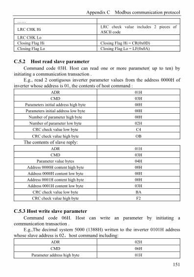
Appendix C Modbus communication protocol
151
……
LRC CHK Hi LRC check value includes 2 pieces of ASCII code
LRC CHK Lo Closing Flag Hi Closing Flag Hi = CR(0x0D) Closing Flag Lo Closing Flag Lo = LF(0x0A)
C.5.2 Host read slave parameter
Command code 03H. Host can read one or more parameter( up to ten) by initiating a communication transaction .
E.g., read 2 contiguous inverter parameter values from the address 0000H of inverter whose address is 01, the contents of host command :
ADR 01H
CMD 03H
Parameters initial address high byte 00H
Parameters initial address low byte 00H
Number of parameter high byte 00H
Number of parameter low byte 02H
CRC check value low byte C4
CRC check value high byte OB
The contents of slave reply: ADR 01H
CMD 03H
Parameter value bytes 04H
Address 0000H content high byte 00H
Address 0000H content low byte 00H
Address 0001H content high byte 00H
Address 0001H content low byte 03H
CRC check value low byte BA
CRC check value high byte F2
C.5.3 Host write slave parameter
Command code 06H. Host can write an parameter by initiating a communication transaction .
E.g.,The decimal system 5000 (1388H) written to the inverter 0101H address whose slave address is 02,host command including:
ADR 02H
CMD 06H
Parameter address high byte 01H
Appendix C Modbus communication protocol
152
Parameter address low byte 01H
Parameter value high byte 13H
Parameter value low byte 88H
CRC check value low byte D4
CRC check value high byte 93
The contents of slave reply: ADR 02H
CMD 06H
Parameter address high byte 01H
Parameter address low byte 01H
Address 0101H content high byte 13H
Address 0101H content low byte 88H
CRC check value low byte D4
CRC check value high byte 93
C. 6 Data communication address allocation
C.6.1 Function code F00-F26 group communication address Inverter function parameter’s MODBUS communication address addressing
process follows PPnn way: PP means high byte of the address, corresponding to function parameter’s group number; nn means low byte of the address, corresponding to function code parameter’s group internal code. For example: F3.21 function code’s communication address is 0315H, 03H is the hex form of group number 3, 15H is the hex form of group internal code 21.
F00.00~F26.17 communication address is 0000H~1A11H, F26 group fault record parameter start address is 1A00H.
C.6.2 Control command and status word communication address
Variable
Name
Communica
tion address
Reading-writing
attribute
Command data or response value
meaning
Run command
word 1E00H
Reading and writing
1: reserved 2: Jog stop command 3: forward JOG run 4: reversal JOG run 5: run 6: stop 7: forward run 8: reversal run

Appendix C Modbus communication protocol
153
9: fault reset 10: reserved
Serial port
value setting
1E01H Reading and
writing
F01.02 while hundreds place=0, 5000 represents 50.00 Hz F01.02 while hundreds place=1, 10000 represents F01.11
Inverter status
1E02H Reading only
BIT0: bus voltage set BIT1: the ordinary run command effectively BIT2: JOG command effectively BIT3: Running BIT4: the current running direction is reverse BIT5: the operating instructions is reverse direction BIT6: deceleration braking BIT7: acceleration BIT8: deceleration BIT9: alarm BIT10: fault BIT11: current limit BIT12: fault self recovery BIT13: self tuning BIT14: Free stop State BIT15: speed tracking start
Alarm code
1E03H Reading only 0: no alarm 1 ~ 50: the current alarm code
C.6.3 Monitor parameter communication address
Variable
name
Communication
address
read-write
attribute Command data or response value
C-00 1C00H Reading Monitoring parameters 1
C-01 1C01H Reading Monitoring parameters 2
C-02 1C02H Reading Monitoring parameters 3
C-03 1C03H Reading Monitoring parameters 4
C-04 1C04H Reading Monitoring parameters 5
C-05 1C05H Reading Monitoring parameters 6
Modbus communication address 1E01(frequency setting)can be torque setting and pressure setting address。
Note

Appendix C Modbus communication protocol
154
C.6.4 Inside hidden parameters
Variable name Communication
address
read-write
attribute
means of command data
or response value PID Communication
presetting value 1D00H read-write
Range:0~1000 (1000 represents 10.00V)
Torque communication presetting value
1D01H read-write Range:0~2000(2000 represents 200.0% rated motor torque)
Communication AO1 given value
1D02H read-write Range: 0~4000(4000 represents 10.00V or 20.00mA)
Communication AO2 given value
1D03H read-write Range: 0~4000 (4000 represents 10.00V or 20.00mA)
Communication EAO1 given value
1D04H read-write Range: 0~4000 (4000 represents 10.00V or 20.00mA)
Communication EAO2 given value
1D05H read-write Range: 0~4000 (4000 represents 10.00V or 20.00mA)
Communication DO given value
1D06H read-write Range: 0~4000 (4000 represents 10.00V or 20.00mA)
Communication EDO given value
1D07H read-write Range: 0~4000 (4000 represents 10.00V or 20.00mA)
The communication output terminal given
value 1D08H read-write
BIT0:Y1 BIT1:Y2 BIT2:Y3 BIT3: Y4 BIT4: RLY BIT5: EY1 BIT6: EY2 BIT7: EY3 BIT8: EY4 BIT9: ERLY1 BIT10: ERLY2
Communication virtual input terminal
given value 1D09H read-write
BIT0:CX1 … BIT7: CX8
Positive torque limited frequency
1D0AH read-write Range: 0~60000 (60000 represents 600.00Hz)
Negative torque limited frequency
1D0BH read-write Range: 0 ~ 60000(60000 represents 600.00Hz)
Appendix C Modbus communication protocol
155
Process PID feedback voltage
1D0CH read-write Range: 0 ~ 4000(4000 represents 10.00V)
Reserved 1D0DH /
C.7 Communication error processing Inverter receiving data packet detection error, it finds reading &writing
parameter address or parameter value invalid, so reply to the host with communication error response packet. Communication error response packet (host command code +80H) as command code, with 1 byte error code.
Format for communication error response packet as follows:
ADR 01H
CMD 83H/86H
Communication error code 01H~06H (for details, please check below table)
Low byte of CRC checksum Obtain by calculating
High byte of CRC checksum Obtain by calculating
Meaning for each communication error code value as follows: Communication error code
value Communication error type Priority
0x01 CRC checksum error 1 0x02 Command code illegal 2 0x03 Register address visited illegal 3 0x04 Value to register illegal 4 0x05 Not allow to modify parameters 5 0x06 Register number read illegal 6
C.8 Data frames examples
C.8.1 RTU Mode
1. Start 1# inverter running
Data Field Slave
Address Order code
Register address
High byte
Register address
Low byte
Data High byte
Low High byte
CRC high bit
CRC Low bit
Host command
frames 01 06 1E 00 00 05 4F E1
Slave respond frames
01 06 1E 00 00 05 4F E1

Appendix C Modbus communication protocol
156
2. Stop 1# inverter running
Data Field Slave
Inverter Address
Order code
Register address
High byte
Register address
Low byte
Data High byte
Low High byte
CRC high bit
CRC Low bit
Host command
frames 01 06 1E 00 00 06 0F E0
Slave respond frames
01 06 1E 00 00 06 0F E0
3. Set 1# inverter given value to 50Hz
Data Field Slave
Inverter Address
Order code
Register address
High byte
Register address
Low byte
Data High byte
Low High byte
CRC high bit
CRC Low bit
Host command
frames 01 06 1E 01 13 88 D3 74
Slave respond frames
01 06 1E 01 13 88 D3 74
4. Read 1# inverter running state
Data Field Slave
Inverter Address
Order code
Register address
High byte
Register address
Low byte
Data High byte
Low High byte
CRC high bit
CRC Low bit
Host command
frames 01 03 1E 02 00 01 23 E2
Slave respond frames
01 03 (Respond value
byte quantity) 0200 01 79 84
C.8.2 ACSII Mode
Host read Slave, command code: 03

Appendix C Modbus communication protocol
157
The host frame
The host frame format
Fram
e begin
sym
bol
Slave ad
dress
Slave ad
dress
Com
man
d cod
e
Com
man
d cod
e
Register ad
dress
Register ad
dress
Register ad
dress
Register ad
dress
Register n
um
ber
Register n
um
ber
Register n
um
ber
Register n
um
ber
Ch
eckou
t
check
out
En
din
g symb
ol
Send byte
1 2 2 4 4 2 2
Remark: Begin symbol:
The lower computer judge the frame header of ASCII based on this. It is:’:’ Slave address:
Single inverter ID code,range:0~247. Thereinto, 0 is broadcast address. Broadcast address can control all the lined
Slave simultaneously,and the Slave will not send back any Data to the host. That means the Slave only accept and do not send.
Modbus protocol without host address. Command code:
Reading the command of parameter or data from inverter ,the value is:’0’’3’. Register address:
The internal memory address of inverter function parameter is of 4 byte, which is ASCII mode transformed from Hexadecimal.Corresponding relation between specific parameters and memory address can be seen in the later table. Register number:
The number of parameters read by a frame, it is 4 byte. It is ASCII mode transformed from Hexadecimal. Checksum:
From “slave address” to the character before checksum, the LRC checksum of the character string. Function terminal can be seen on the end of the text. Ending code:
Enter, line break. is:0x0D,0x0A
Response frame
Response frame format
Fram
e b
egin
s ymb
ol
Slave
add
ress
Slave
add
ress
Com
man
d
code
Com
man
d
code
Data b
yte
Data b
yte
Data strin
g valu
e
check
sum
check
sum
En
din
g cod
e

Appendix C Modbus communication protocol
158
Send byte
1 2 2 2 N*2 2 2
Remark: Begin code:
The lower computer judge the frame of ASCII frame. This is :’:’ Slave address:
Single inverter ID code,range:0~247. Thereinto, address 0 is broadcast address. Broadcast address can control all the
lined Slave simultaneously,and the Slave will not send back any Data to the host. That means the Slave only accept and do not send.
Modbus protocol is without host address. Command code:
The command of reading parameter or data from inverter, the value is:’0’’3’. Data byte:
The number of parameters read by a frame. It is 4 byte, which is ASCII mode transformed from hexadecimal. Data string value:
The detail return Data,the length of Data string is the register address “Data byte”, which is ASCII mode transformed from hexadecimal. Range: 4~40 byte Checksum:
From “slave address” to the character before checksum, the LRC checksum of the character string.The function terminal can be seen in the later text.
Ending symbol: enter, line break. Is 0x0D,0x0A The followings are the example of command frame and return frame, all the
Data are ASCII character. Inquiry frame:
: 0 1 0 3 0 0 0 1 0 0 0 1 F A \n\r (The detail introduction of every byte) “:”: beginning symbol 0 1: Slave address 0 3: Read the command 0 0 0 1: Storage address of reading parameter 0 0 0 1: The number of reading the parameter F A:0 1 0 3 0 0 0 1 0 0 0 1 for LRC checksum. 0xFA = 0x100 - (0x01 + 0x03 + 0x00 + 0x01 + 0x00 + 0x01)
Response frame: : 0 1 0 3 0 2 0 0 3 3 C 7 \n\r (The detail introduction of every byte) “:”: beginning symbol 0 1: Slave address

Appendix C Modbus communication protocol
159
0 3:read the command 02:The byte length of return parameter Data. 0 0 33:return parameter,current storage value C 7: 0 1 0 3 0 2 0 0 3 3 for LRC checksum. 0xC7 = 0x100 – (0x01 + 0x03 + 0x02 + 0x00 + 0x033) The main frame writes slave address single register, command code: 06
The host frame
The host frame format
Fram
e begin
sym
bol
Slave ad
dress
Slave ad
dress
Slave ad
dress
Com
man
d cod
e
Register ad
dress
Register ad
dress
Register ad
dress
Register ad
dress
Data
Data
Data
Data
Ch
eckou
t
check
out
En
din
g symb
ol
Send byte 1 2 2 4 4 2 2
Remark: Slave address:
Single inverter ID code,range:0~247.Thereinto, address 00 is broadcast address. Command code:
Read parameter from inverter or command of Data, the value is:06 Register address:
The storage address of inverter function parameter, is double byte. The high byte is in the front and the low byte is in the back.
The detail relation between parameter and storage address can be seen in the later excel. Data:
The new value of revised parameter. Checksum:
From “slave address” to the character before checksum, the LRC checksum of the character string.
Response frame
Response frame format
Fram
e begin
sym
bol
Slave ad
dress
Slave ad
dress
Com
man
d cod
e
Com
man
d cod
e
Register ad
dress
Register ad
dress
Register ad
dress
Register ad
dress
Data
Data
Data
Data
Ch
eckou
t
Ch
eckou
t
En
din
g symb
ol

Appendix C Modbus communication protocol
160
Send byte 1 2 21 4 4 2 2
Remark: Slave address:
Single inverter ID code,range:0~247.Thereinto, address 00 is broadcast address. Command code:
Read parameter from inverter or command of Data, the value is:06 Register address:
The storage address of inverter function parameter, is double byte. The high byte is in the front and the low byte is in the back.
The detail relation between parameter and storage address can be seen in the later excel. Data:
The new value of revised parameter. Checksum:
From “slave address” to the character before checksum, the LRC checksum of the character string.
The followings are the example of command frame and return frame, all the Data are ASCII character. Inquiry frame:
: 0 1 0 6 0 1 0 1 1 3 8 8 5 C \n\r (The detail introduction of every byte) “:”: beginning symbol 0 1: Slave address 0 6:write command 0 1 0 1:storage address of writing parameter 1 3 8 8:the value of writing parameter 5C: 0 1 0 6 0 1 0 1 1 3 8 8 for LRC checksum. 0x5C = 0x100 - (0x01 + 0x06 + 0x01 + 0x01 + 0x13 + 0x88)
Response frame: :0 1 0 6 0 1 0 1 1 3 8 8 5 C \n\r (Detail introduction of every byte) “:”: beginning symbol 0 1: Slave address 0 6:write command 0 1 0 1:storage address of writing parameter 1 3 8 8:the value of writing parameter 5C: 0 1 0 6 0 1 0 1 1 3 8 8 for LRC checksum. 0x5C = 0x100 - (0x01 + 0x06 + 0x01 + 0x01 + 0x13 + 0x88)
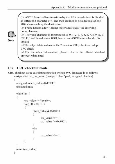
Appendix C Modbus communication protocol
161
C.9 CRC checkout mode CRC checkout value calculating function written by C language is as follows:
unsigned int cal_crc_value (unsigned char *pval, unsigned char len) unsigned int crc_value=0xFFFF; unsigned int i; while(len--) crc_value ^= *pval++; for(i=0; i<8; i++) if(crc_value & 0x0001) crc_value >>= 1; crc_value ^= 0xA001; else crc_value >>= 1; return(crc_value);
⑴ ASCII frame realizes transform by that 8Bit hexadecimal is dividedas different 2 character of 4, and then grouped as hexadecimal of one 8Bit when reaching the destination. ⑵ Frame header, add“:”, frame footer adds“0xda” the enter line break character. ⑶ The valid character in the protocol is: 0, 1, 2, 3, 4, 5, 6, 7, 8, 9, A, B,C,D,E,F and hexadecimal 0DH, lower case ASCII letter a,b,c,d,e,f is invalid.
⑷ The subject data volume is the 2 times as RTU, checksum adopt LRC check.
For the other information, please⑸ refer to the official standard protocol when need.
Note

Appendix D Braking unit and braking resistance
162
Appendix D Braking unit and braking resistance
D.1 Braking unit and braking resistance The motor’s electric potential energy will charge inverter’s capacitance up
reversely if speed of the motor descends too quickly or load of the motor wobbles too quickly while the inverter is running, which will increase the voltage upon power modules suddenly and is easy to make the inverter damaged. The inverter will control it according to load size and performance. You only need to connect external braking resistance to realize timely energy discharge when the braking function is needed. To connect external resistance is a kind of energy consumption braking mode, as all the energy is consumed by the braking resistance.
EN630/EN650A-2S0004~EN630/EN650A-2S0015, EN630/EN650A-4T0007, EN630/EN650A-4T0015 have been configured built-in braking unit.
When braking function needed, please connect external braking resistance according to below table.
Configuration table of braking unit and braking resistor configuration as well as circumscribed braking resistor
Inverter type
Inbuilt
braking
unit
Inbuilt
braking
resistor
External
braking
resistor
Quantity
Power of
braking
resistor
(50%
braking
rate)
Power of
braking
resistor
(10%
braking
rate)
EN630/EN650A-2S0004 Inbuilt No ≥400Ω 1PCS ≥500W ≥100W
EN630/EN650A-2S0007 Inbuilt No ≥400Ω 1PCS ≥500W ≥100W
EN630/EN650A-2S0015 Inbuilt No ≥400Ω 1PCS ≥500W ≥100W
EN630/EN650A-4T0007 Inbuilt No ≥500Ω 1PCS ≥600W ≥120W
EN630/EN650A-4T0015 Inbuilt No ≥500Ω 1PCS ≥600W ≥120W

ShenZhen Encom Electric Technologies CO.,LTD.
Address: Floor 6, Building 2 West, Pingshan Minqi Science &
Technology Park, Taoyuan Str., Nanshan District, Shenzhen, China
Website: http://www.encvfd.com
Email: [email protected] [email protected]
Tel: +86-755-26984485 Fax: +86-755-26985120