user’s manual: demonstration board industrial analog and power · 2019-08-02 · user’s manual...
TRANSCRIPT
User’s M
anual
All information contained in these materials, including products and product specifications,represents information on the product at the time of publication and is subject to change byRenesas Electronics Corp. without notice. Please review the latest information published byRenesas Electronics Corp. through various means, including the Renesas Electronics Corp.website (http://www.renesas.com).
Rev.1.00Renesas Electronics Corporationwww.renesas.com
HIP4086DEMO1ZUser’s Manual: Demonstration Board
Industrial Analog and Power
Aug.2.19

AN1829 Rev.1.00 Page 2 of 35Aug.2.19
HIP4086DEMO1ZDemonstration Board
User’s Manual
The HIP4086DEMO1Z is a general purpose 3-phase BLDC motor drive with a microprocessor based controller. Hall effect shaft position sensors control the switching sequence of the three 1/2 bridge outputs. The bridge voltage can vary between 12V and 60V and the maximum summed bridge current is 20A (with sufficient air flow). This motor drive can be used as a design reference for multiple applications including e-bikes, battery powered tools, electric power steering, wheel chairs, or any other application where a BLDC motor is used. Because this demonstration board is primarily intended to highlight the application of the HIP4086 3-phase MOSFET driver with no specific application targeted, the control features are limited to simple functions, such as start/stop, reverse rotation, and braking. Open-loop speed control is implemented. More advanced control features, such as torque control, speed regulation, and regenerative braking are not implemented because these methods require close integration with the characteristics of the load dynamics.
This user manual covers the design details of the HIP4086DEMO1Z with a focus on the design implementation of the HIP4086 driver using recommended support circuits.
This guide also covers the design method of the bipolar current sensing feature. Presently, current sensing on this demonstration board is used only for pulse-by-pulse current limiting. However, an analog signal proportional to the motor current is available on board as a design reference.
The microcontroller firmware is also provided as a reference but the only support offered by Renesas is for bug corrections and for adding more switching sequences. See Microchip for details on the PIC18F2431 usage.
Specifications
Related LiteratureFor a full list of related documents, visit our website:
• HIP4086, ISL6719, ISL8560, ISL28134, ISL28214 device pages
Important NoteBecause Hall sensor switching logic sequences for BLDC motors are not all the same, this demo board supports most, if not all, variations of sequence logic. See the sequence charts in “Selecting the Correct Switching Sequence” on page 17 to verify that your desired sequence is implemented. If you require a different sequence for your specific motor application or if you need help identifying the correct switching sequence for your specific motor, please contact Renesas prior to ordering this demonstration board for possible support for a new switching sequence.
Motor topology 3-phase BLDC motor with Hall sensors
Operating voltage range 15VDC to 60VDC
Maximum bridge current 20A (with sufficient air flow)
Hall sensor bias voltage 5V
PWM switching frequency 20kHz

HIP4086DEMO1Z
AN1829 Rev.1.00 Page 3 of 35Aug.2.19
Figure 1. HIP4086DEMO1Z Block Diagram
HIP4086DEMO1Z
ISL8560 +5V Buck Regulator HIP4086
3-Phase MOSFET
Driver
ISL6719 Linear +12V
Regulator
Controller
LEDsDipSwitches
Push Buttons
15V to 60V
3-Phase Bridge BLDC Motor
ISL28134ISL28214Current
Limitand
Monitor
Hall Inputs
4
3
6
6
2
3

HIP4086DEMO1Z 1. Functional Description
AN1829 Rev.1.00 Page 4 of 35Aug.2.19
1. Functional Description
1.1 Required and Recommended Lab Equipment• Lab supply (or battery), 15V minimum to 60V absolute maximum. The current rating of the lab supply must have
sufficient capacity for the motor being tested. Note: If a battery is the power source, Renesas highly recommends that an appropriate fuse is used.
• Bench fan
• Test motor
• Multichannel oscilloscope, 100 MHz
• Multimeter
• Temperature probe (optional)
CAUTION: If the HIP4086DEMO1Z is used for an extended period at high power levels, it may be necessary to use a fan to keep the temperature of the bridge FETs to less than +85°C (as measured on the heat sink plane).
1.2 Setup and Operating Instructions1. Connect the 3-phase motor leads to the MA, MB, and MC terminal blocks. For high current applications, it is
recommended that both terminals of each block are used. It is also recommended that during initial setup the motor is not mechanically loaded.
2. Connect the HALL sensor leads of the motor to the HA, HB, and HC terminals. The +5V bias and ground leads must all be connected.
3. Rotate the R13 potentiometer to the left (CCW) until it clicks. This sets the starting voltage on the motor to a minimum.
4. Setup the dip switch for the correct switching sequence (see the switching sequence tables in Figures 18 and 19).
5. With a lab supply turned off but previously set to the desired bridge voltage, connect the lab supply (or battery) to the +BATT and -BATT terminal block.
6. Ensure that the motor is securely mounted prior to proceeding with the following steps. Also, do not exceed the maximum rated RPM of your motor.
7. Turn on the lab supply. Observe that the four LEDS turn on and off, one after another. This initial flash of the LEDs indicates that power has been applied. After the initial flash, all LEDs are off. Operation of the motor is now possible. Note that the dip switch options are read at initial turn-on and changing the settings after power is applied has no effect. As an alternative to cycling power, the reset push button can be pressed to re-read the dip switch settings.
8. Press the Start/Stop push button once. The Run LED (LED0) blinks, indicating that the motor has been started. At this point, the motor may not be rotating because minimal voltage is being applied to the motor.
9. Slowly increase the voltage on the motor by rotating the potentiometer, R13, to the right (CW). At some point the motor starts to rotate slowly. The actual starting voltage is dependent on the specific motor being used.
LED0LED2LED3 LED1
At initial turn on, LEDs turn on and off one at a time starting with led0
LED0LED2LED3 LED1
While the motor is rotating, the Run LED is blinking
RunReverseBrakeILIMIT
HIP4086DEMO1Z 1. Functional Description
AN1829 Rev.1.00 Page 5 of 35Aug.2.19
10. If the motor is vibrating back and forth instead of rotating, it is possible that the Hall sensors or the motor leads were not connected correctly. If the correct switching sequence has been selected, swap two of the motors’ leads (or swap two of the Hall sensor leads).
11. Continue to rotate the potentiometer until the motor is running at a moderate speed of roughly 25%. Do not run the motor with maximum voltage until the setup check-out is completed.
12. Press the START/STOP push button again. The motor free wheels to a stop and the blinking LED0 turns off.
13. Press the START/STOP button again. The motor accelerates to the previous run speed (assuming that the potentiometer was not rotated). The blinking LED0 also turns on.
14. While the motor is running, press the Reverse button. The Run LED (LED0) turns off and the Reverse LED (LED1) turns on without blinking. After a short pause while the motor is freewheeling to a stop, the motor restarts rotating in the opposite direction. The Run LED is blinking and the Reverse LED continues to be on.
15. Press the Reverse button again. As before, the motor stops. But this time the Reverse LED turns off. After a pause, the motor restarts but this time rotating in the forward direction.
16. While the motor is running, the motor can be hard braked by pressing the Brake push button. The Brake LED (LED2) is on without blinking. When the motor is restarted, the Brake LED turns off.
CAUTION: The braking method implemented turns on all of the low-side bridge FETs simultaneously. This forces the motor to a very rapid stop. If the motor is loaded, or if the motor is not designed for a rapid stop, mechanical damage to the motor or the load can result. If you are not sure about using this braking method, only apply the brake when the motor speed is relatively slow.
17. If while operating, the motors turns off and the ILIMIT LED (LED3) is blinking, the current limit shut-down has been activated after 255 consecutive pulse-by-pulse current limits. This can happen if the motor speed is accelerated too quickly, or if there is a fault with the motor or connections, or if the motor is stalled.
It is now safe to proceed with testing at higher power levels speeds.
1.3 Test ModeTo validate the correct performance of the HIP4086DEMO1Z, a built-in test procedure can be used to verify that the board is fully functional. A 50V, 200mA lab supply and an oscilloscope are necessary to perform this test. No
LED0LED2LED3 LED1
RunReverseBrakeILIMIT
LED0LED2LED3 LED1
RunReverseBrakeILIMIT
LED0LED2LED3 LED1
RunReverseBrakeILIMIT
Blinking
LED0LED2LED3 LED1
RunReverseBrakeILIMIT
led0led2 led1
RUNREVERSEBRAKEILIMIT
led3

HIP4086DEMO1Z 1. Functional Description
AN1829 Rev.1.00 Page 6 of 35Aug.2.19
motor is required and should not be connected. Each individual test section must be valid before proceeding to the next step. Stop testing at any failure.
1.3.1 Test Mode Setup1. Connect a ~75mm (3 inch) wire to the GND terminal close to the HA, HB, HC terminal block.
2. Set up a scope with the vertical scale = 20V/div and the time base = 10µs/div. Three probes are recommended but not absolutely necessary.
3. Adjust the lab supply to the 50VDC and 200mA current limit.
4. With the lab supply turned off, connect to the +BATT and -BATT terminal inputs of the HIP4086DEMO1Z board.
5. Set dip switch positions 1 through 4 to on.
6. While simultaneously pressing the Brake and Reverse push buttons, turn on the lab supply.
7. If LED0 and LED3 are flashing or if no LEDs are on, the test mode was not initiated correctly, the board is faulty, or the microcontroller is not programmed. To confirm, restart the test mode setup. If one or more LEDS are on without flashing, the test mode is now active. At this point the binary combination of the on LEDs indicates the version number of the firmware (see Figure 2). Figure 3 shows other examples of faulty setup or failed test results.
1.3.2 Push-Button Test1. Press the START/STOP button. All four LEDs should turn on.
2. Press the START/STOP button again. Led0 should turn off.
3. Press the Reverse button. Led1 should turn off.
4. Press the Brake button. Led2 should turn off.
5. Press the Brake button again. Led3 should turn off. At this point all four LEDs are off and correct operation of the push buttons is confirmed.
Figure 2. Code Version Numbers Figure 3. Examples of LED Test Status
led0led1led2led3 Code version 1
led0led1led2led3 Code version 2
led0led1led2led3 Code version 3
led0led1led2led3 Code version 4
led0led1led2led3 Code version 5
led0led1led2led3 Code version 6
led0led1led2led3 Code version 15
led0led1led2led3 Code version 7
led0led1led2led3 Code version 8
led0led1led2led3 Code version 9
Note that the LEDs are binary encoded.
led3 led2 led1 led0
LED1LED2Invalid test mode configuration
Current monitor test failure
Red arrows indicate a flashing LED
LED3 LED2 LED1 LED0
LED3 LED0
Cuccessful test Mode completion
LED1LED2LED3 LED0
Blue arrows indicate the movement of the flashing LED
LED1LED2LED3 LED0Valid test mode startup, no flashing

HIP4086DEMO1Z 1. Functional Description
AN1829 Rev.1.00 Page 7 of 35Aug.2.19
1.3.3 Hall Inputs and Bridge Tests
1.3.3.1 MA Output Test
1. Using the 75mm wire, short the HA terminal input to ground. LED0 should turn on.
2. While the HA input is grounded, observe the following waveforms in Figure 4, on the MA, MB, and MC terminals.
3. Figure 5 illustrates incorrect waveforms. There should not be any switching on MB and MC while MA is low. At the very edge of MA falling, there may be a small amount of induced switching noise.
4. While the HA input is grounded, observe that the lab supply current is < 45mA.
Figure 4. Waveforms on MA, MB, and MC with HA Grounded
Figure 5. Waveforms on MA, MB, and MC with HA Grounded
MA
MB
MC
MA
MB
MC
HIP4086DEMO1Z 1. Functional Description
AN1829 Rev.1.00 Page 8 of 35Aug.2.19
1.3.3.2 MB Output Test
1. Using the 75mm wire, short the HB terminal input to ground. Led1 should turn on.
2. While the HB input is grounded, observe the following waveforms on the MA, MB, and MC terminals. As the example in Figure 6 shows, there should be no switching disturbances on MC and MA.
3. While the HB input is grounded, observed that the lab supply current is <45mA.
1.3.3.3 MB Output Test
1. Using the 75mm wire, short the HC terminal input to ground. Led2 should turn on. After a short pause, LED3 also turns on. At this point, all four LEDs are on.
2. While the HC input is grounded, observe the following waveforms on the MA, MB, and MC terminals. As the example in Figure 7 shows, there should be no switching disturbances on MB and MA.
3. While the HC input is grounded, observe that the lab supply current is < 45mA.
Figure 6. Waveforms on MA, MB, and MC with HB Grounded
Figure 7. Waveforms on MA, MB, and MC with HC Grounded
MA
MB
MC
MA
MB
MC

HIP4086DEMO1Z 1. Functional Description
AN1829 Rev.1.00 Page 9 of 35Aug.2.19
1.3.4 Dip Switch Test1. Move each dip switch, one at a time starting with position 1, to the off position.
2. Observe that LED0, LED1, LED2, and LED3 turn off one at a time in sync with the dip switches being turned off.
1.3.5 Potentiometer Test1. After a short pause, all LEDs turn on if the potentiometer is turned fully to the right (CW). If the LEDs are not
on, rotate the potentiometer to the right until all LEDs turn or when the potentiometer starts to click. If all LEDs do not turn on, the board is faulty.
2. After all the LEDs turn on, rotate the potentiometer to the left (CCW). Observe that LED3, LED2, LED1, and LED0 turn off sequentially as the potentiometer is rotated towards the minimum voltage setting.
1.3.6 Current Monitor Test1. This final test is performed automatically after the potentiometer test. No inputs from the test operator are
necessary. If successful, all four LEDs are sequentially flashing one at a time. If not successful, all four LEDS flash simultaneously.

HIP4086DEMO1Z 2. Theory of Operation
AN1829 Rev.1.00 Page 10 of 35Aug.2.19
2. Theory of OperationThe HIP4086DEMO1Z demonstration board is a general purpose 3-phase BLDC motor controller. Three half bridge power circuits drive the motor as shown in Figure 8.
Three 6-step bridge state logic diagrams, illustrated in Figure 9 on page 11, drive the motor. The bridge state logic diagrams represents the logic status of the each half bridge but the actual voltage applied to the motor appears much differently. Figure 10 on page 11 illustrates the bridge status logic vs the actual voltage waveforms applied to each motor lead.
The HIP4086 has six driver outputs, AHO, ALO, BHO, BLO, CHO, and CLO, to control the six bridge FETs individually. If the gate drives for both FETs of one half bridge are low, current does not flow in the corresponding motor lead (high impedance or Hi-Z). If the gate drive for the low FET is high and the gate drive for the high FET is low, the phase node of that half bridge, and the corresponding motor lead, is connected to ground (Low). If the low and high gate drives are complementary driven, the phase node can be Pulse-Width Modulated (PWM) to control the average voltage on that motor lead.
The motor rotation period and the amplitude of the bridge voltage waveforms are modified by the microcontroller to control the speed of the motor. Pulse-width modulation modifies the amplitude of the voltage waveforms and the motor rotation period is established by the shaft position hall sensors that signal the controller to change the switching sequence. Typical hall sensor logic is illustrated in Figure 9. Each hall logic diagram, HA, HB, and HC, correspond respectively to the bridge state logic diagrams, MA, MB, and MC. For example, the transition of the hall sensor logic, from Step 1 to 2, results with the drive waveform transition of ZLP to PLZ where P, L, and Z define the state of each half bridge.
Figure 8. Basic BLDC Motor Power Topology
BLDC Motor
AHO
ALO BHO
BLO
CHO
CLO

HIP4086DEMO1Z 2. Theory of Operation
AN1829 Rev.1.00 Page 11 of 35Aug.2.19
2.1 Switching Sequence Phase CurrentsThe following motor winding diagrams illustrate how currents flow in a 3-phase BLDC motor during each switching period of the 6-step voltage waveform. These diagrams are for a very simple motor with only six stator poles. Most 3-phase motors have more stator poles (multiples of six) to reduce torque modulation (cogging) but the principles of operation are the same.
Each phase winding is color coded and black arrows indicate the direction of positive current in that winding for each step. As described in Figure 11 on page 12, the half bridge state of each motor lead, MA, MB, or MC, is labeled with P, L, or Z. Observe that the active coils are highlighted. The inactive coils (those with no current) are white.
The dark gray structures are the permanent magnets that are mounted on the light gray rotor. The bold black arrow is the flux vector of the permanent magnets. The bold dark blue arrow is the magnetic flux vector generated by the active coils for each waveform step. The switching step occurs when these two vectors are perpendicular for maximum torque. Notice how the flux vectors are rotating counter clockwise, 60° for each step.
This tutorial for BLDC motors is very fundamental. For more information about a specific motor, please contact the motor manufacturer.
Figure 9. Hall Sensor Logic vs Bridge State Logic Figure 10. Bridge State Logic vs Motor Voltage
000 100 110 111 011 000 100 110 111 011001 001
Hall Sensor Logic
HC
HB
HA
ZLP PLZ PZL ZPL LPZ LZP ZLP PLZ PZL ZPL LPZ LZP
MB
MA
MC
1 2 3 4 5 6 1 2 3 4 5 6
0° 60° 120° 180° 240°
Bridge State Logic: P = PWM, L = Low, Z = off
0° 60° 120° 180° 240° 0°
Sequence Step Numbers
Z
L
P
ZLP PLZ PZL ZPL LPZ LZP ZLP PLZ PZL ZPL LPZ LZP
MB
MA
MC
Bridge State Logic: P = PWM, L = Low, Z = off
Idealized Motor Voltage Waveforms
MC
MB
MA
+Vbat
-Vbat
~ ½ Vbat
20kHz PWM freq.
Motor rotation periodper pole

HIP4086DEMO1Z 2. Theory of Operation
AN1829 Rev.1.00 Page 12 of 35Aug.2.19
Figure 11. Sequence Steps 1 to 3
Figure 12. Sequence Steps 4 to 6
N
N
S
S
N
S
N
S
N
S N
S
N
S N
S
S
S
N
N
2
P
Z
L
3
P
L
Z
N
S
N
S
N
S
N
S
N
S
N
S
N
S
N
S
HC
HBHA
MB
MA
MC
1 2 3
HC
HBHA
MB
MA
MC
HC
HBHA
MB
MA
MC
L
LL
PP
P
Z
Z
Z
Z
ZPP L
L
1
Z L
Neutral
P
Z
P
L
Neutral Neutral
NeutralNeutralNeutral
NeutralNeutral Neutral
Neutral Neutral Neutral
S
N
S
N
S
N
S
N
S
N
S
N
4
Z
L
P
5
L
Z
P
6
L
P
Z
S
S
N
N
N
N
S
S
S
N
S
N
N
S
N
S
N
S
N
S
N
S
N
S
64 5
HCHBHA
MB
MA
MC
HCHBHA
MB
MA
MC
HCHBHA
MB
MA
MC
L Z P
LL
PP Z
Z
Z
Z
Z
P
PP
L
L L
Neutral Neutral Neutral
NeutralNeutralNeutral
Neutral Neutral Neutral
Neutral Neutral Neutral
HIP4086DEMO1Z 2. Theory of Operation
AN1829 Rev.1.00 Page 13 of 35Aug.2.19
2.2 HIP4086 Circuit DescriptionIn the following discussion, xHI, xLI, xHO, xLO, and xHS is a short hand notation where the x can be replaced with A, B, or C. An “x” pin implies that the reference is applicable to the corresponding A, B, or C pins of the driver.
The simplified schematic of Figure 13 illustrates the three power stages of the motor driver. Each phase is identical in component selection. For specific component values and complete circuit details, see “Bill of Materials” on page 21 and “PCB Layout” on page 27.
Series connected gate resistors on each bridge FET reduce the switching speed to help minimize EMI radiating from the power leads to the motor. You can change these values if needed, keeping in mind that if the gate resistors are made larger, the turn off delays of the FETs also increase, which may require additional dead time.
All of the xHS pins have recommended external snubber circuits and negative voltage clamps to ensure that safe operating conditions are always maintained over-temperature and loading conditions.
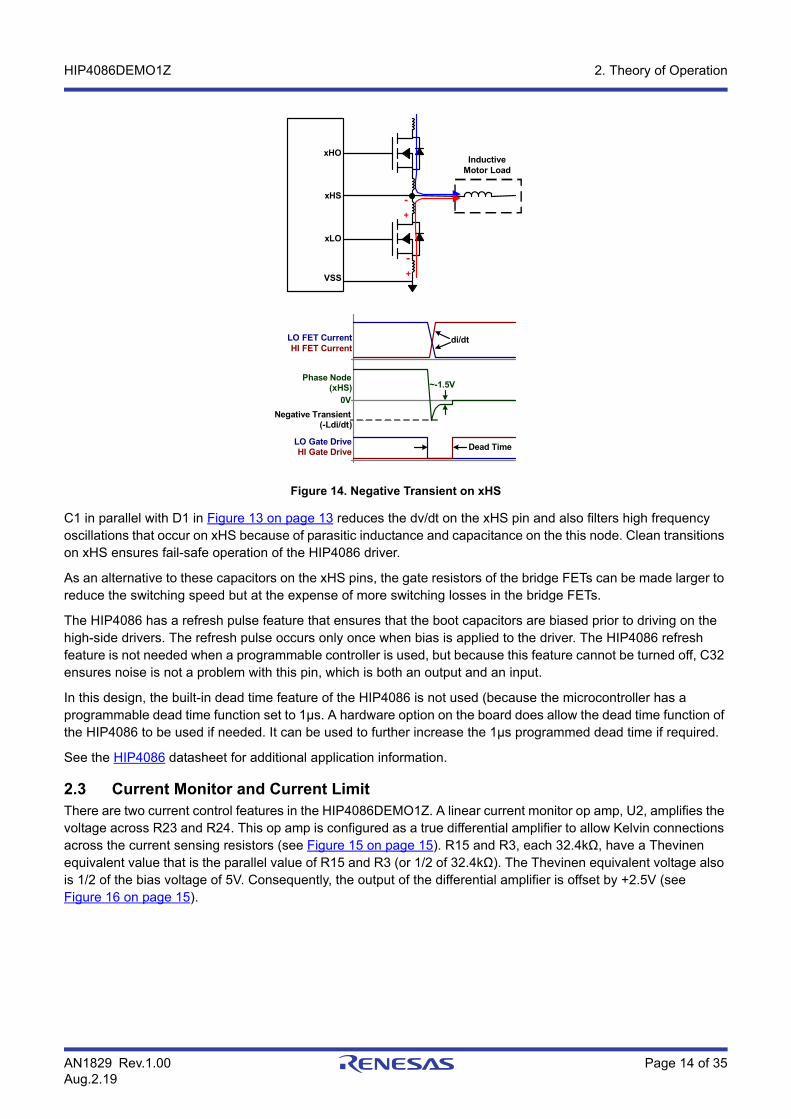
For example, D1 in Figure 13 functions as a negative voltage clamp on the AHS pin. Frequently, circuit designers overlook the negative transients on the xHS pins that occur when the high-side bridge FET turns off. This rapid di/dt transition of the current from Q1 to Q2 develops a negative voltage transient as a result of the parasitic inductance in the low-side FET power current path (see Figure 14 on page 14).
R1 on the AHS pin is necessary to limit the current in D1 during the dead time because without this resistor, D1 is essentially in parallel with the body diode of Q1. During the dead time, the commutating negative current in the body diode results with approximately a -1.5V conduction voltage (with large amplitude motor currents). Because the conduction voltage of D1 (~0.6V) is less than the body diode, R1 limits the current that would flow in D1 during the dead time to safe levels. Note that when the low-side bridge FET is turned on, the negative voltage across the FET is greatly reduced because the conduction voltage of the FET channel is typically much less than the conduction voltage of the body diode. This results with a negative conduction voltage much less than 0.6V and consequently, significant current flows in D1 only during the dead time.
Figure 13. Simplified 3-Phase Bridge
AHO
CLO
BLO
ALO
CHO
BHO
CLI
BLI
ALI
CHI
BHI
AHICHS
AHS
BHS
CHB
AHB
BHB
VDD
RDEL
HIP4086/A
VSS
Motor
VDD VBAT
Current Sense
RFSH
D1
R1
Q1
Q2
C1
C2
HIP4086DEMO1Z 2. Theory of Operation
AN1829 Rev.1.00 Page 14 of 35Aug.2.19
C1 in parallel with D1 in Figure 13 on page 13 reduces the dv/dt on the xHS pin and also filters high frequency oscillations that occur on xHS because of parasitic inductance and capacitance on the this node. Clean transitions on xHS ensures fail-safe operation of the HIP4086 driver.
As an alternative to these capacitors on the xHS pins, the gate resistors of the bridge FETs can be made larger to reduce the switching speed but at the expense of more switching losses in the bridge FETs.
The HIP4086 has a refresh pulse feature that ensures that the boot capacitors are biased prior to driving on the high-side drivers. The refresh pulse occurs only once when bias is applied to the driver. The HIP4086 refresh feature is not needed when a programmable controller is used, but because this feature cannot be turned off, C32 ensures noise is not a problem with this pin, which is both an output and an input.
In this design, the built-in dead time feature of the HIP4086 is not used (because the microcontroller has a programmable dead time function set to 1µs. A hardware option on the board does allow the dead time function of the HIP4086 to be used if needed. It can be used to further increase the 1µs programmed dead time if required.
See the HIP4086 datasheet for additional application information.
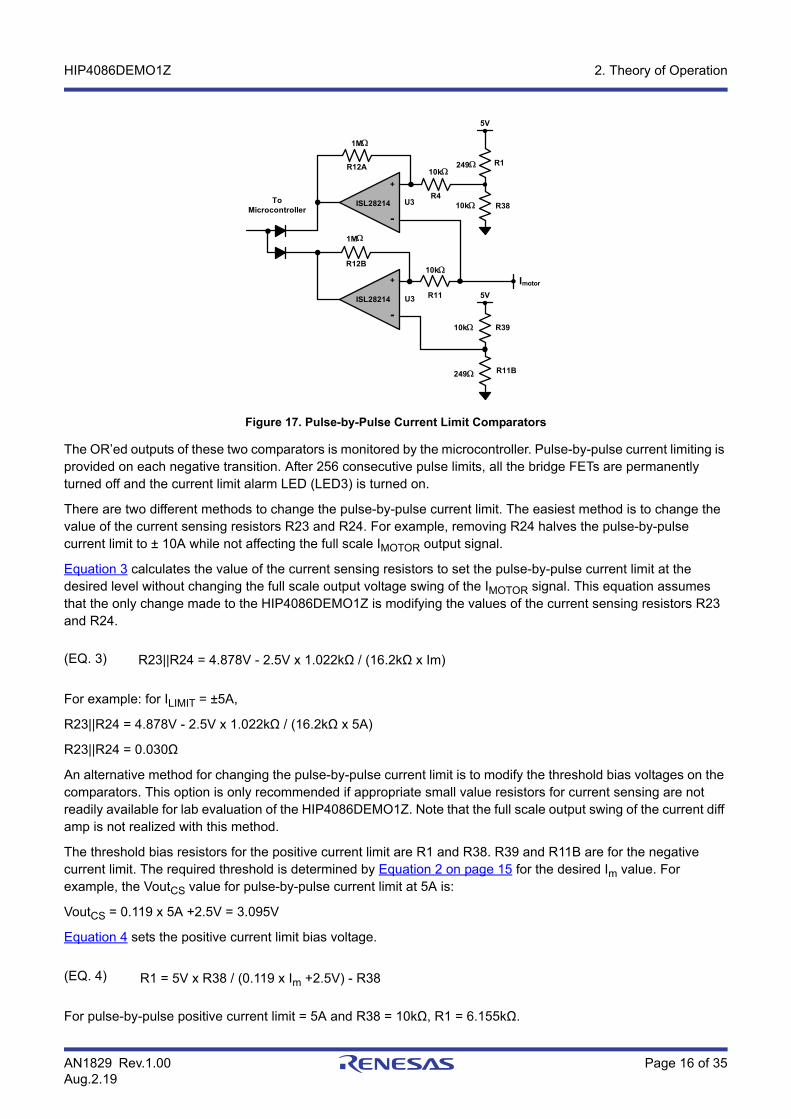
2.3 Current Monitor and Current LimitThere are two current control features in the HIP4086DEMO1Z. A linear current monitor op amp, U2, amplifies the voltage across R23 and R24. This op amp is configured as a true differential amplifier to allow Kelvin connections across the current sensing resistors (see Figure 15 on page 15). R15 and R3, each 32.4kΩ, have a Thevinen equivalent value that is the parallel value of R15 and R3 (or 1/2 of 32.4kΩ). The Thevinen equivalent voltage also is 1/2 of the bias voltage of 5V. Consequently, the output of the differential amplifier is offset by +2.5V (see Figure 16 on page 15).
Figure 14. Negative Transient on xHS
VSS
xHS
xLO
xHOInductive
Motor Load
+
-
+
-
Dead Time
Phase Node (xHS)
LO Gate DriveHI Gate Drive
LO FET CurrentHI FET Current
di/dt
~-1.5V
0V
Negative Transient (-Ldi/dt)

HIP4086DEMO1Z 2. Theory of Operation
AN1829 Rev.1.00 Page 15 of 35Aug.2.19
The current monitor output, IMOTOR, digitized by the microcontroller, can be used to control the torque of the motor or to limit the battery recharging current during regenerative braking. Because of the offset voltage on the current monitor output, signals above 2.5VDC represents positive motor current and signals less that 2.5VDC represent negative motor current. Note: This hardware feature is provided for customer use but is not implemented in the microcontroller firmware.
The output voltage of the differential amplifier is:
where IM is the bridge current (motor current), R12||R14 = R15||R3, and (R17+R21) = (R18+R22) (as required for the differential amp topology).
Using the defaults values of the HIP4086DEMO1Z:
VoutCS = [(16.2kΩ))/(1022)] x Im x (0.0075) + 32.4kΩ/(64.8kΩ) x 5V
or
For 20A, VoutCS = 4.878V. For -20A, VoutCS= 0.122V.
The Imotor signal is monitored by two comparators (see Figure 17 on page 16). The output of the upper U3 comparator is biased to go low when the motor current > 20A. Conversely, the output of the lower comparator is biased to go low when the motor current is ≤ 20A.
Figure 15. Differential Current Monitor Amplifier Figure 16. Thevinen Equivalent Differential Amplifier
U2R17 R21
R18 R22
R14
R12
R15
R3
5V
ISL28134
32.4k
Filter Capacitors are not Shown.
R23 R24
From Bridge
0.0150.015IMOTOR
+
-
32.4k
32.4k
32.4k
511 511
511
511U2
R17+R21
R18+R22
R12||R14
R15||R3
2.5VTHEV
ISL28134
Note that resistors labeled Rx||Ry represent a parallel equivalent resistor of Rx and Ry. Rx+Ry represents the series combination of Rx and Ry.
R23||R24
From Bridge
0.0075IMOTOR
+
-
1022
1022
16.2k
16.2k
(EQ. 1) VoutCS = [(R12||R14)) / (R17+R21)] x IM x (R23||R24)+ R3 / (R3+R15) x 5V
(EQ. 2) VoutCS = 0.119 x IM+2.5V
HIP4086DEMO1Z 2. Theory of Operation
AN1829 Rev.1.00 Page 16 of 35Aug.2.19
The OR’ed outputs of these two comparators is monitored by the microcontroller. Pulse-by-pulse current limiting is provided on each negative transition. After 256 consecutive pulse limits, all the bridge FETs are permanently turned off and the current limit alarm LED (LED3) is turned on.
There are two different methods to change the pulse-by-pulse current limit. The easiest method is to change the value of the current sensing resistors R23 and R24. For example, removing R24 halves the pulse-by-pulse current limit to ± 10A while not affecting the full scale IMOTOR output signal.
Equation 3 calculates the value of the current sensing resistors to set the pulse-by-pulse current limit at the desired level without changing the full scale output voltage swing of the IMOTOR signal. This equation assumes that the only change made to the HIP4086DEMO1Z is modifying the values of the current sensing resistors R23 and R24.
For example: for ILIMIT = ±5A,
R23||R24 = 4.878V - 2.5V x 1.022kΩ / (16.2kΩ x 5A)
R23||R24 = 0.030Ω
An alternative method for changing the pulse-by-pulse current limit is to modify the threshold bias voltages on the comparators. This option is only recommended if appropriate small value resistors for current sensing are not readily available for lab evaluation of the HIP4086DEMO1Z. Note that the full scale output swing of the current diff amp is not realized with this method.
The threshold bias resistors for the positive current limit are R1 and R38. R39 and R11B are for the negative current limit. The required threshold is determined by Equation 2 on page 15 for the desired Im value. For example, the VoutCS value for pulse-by-pulse current limit at 5A is:
VoutCS = 0.119 x 5A +2.5V = 3.095V
Equation 4 sets the positive current limit bias voltage.
For pulse-by-pulse positive current limit = 5A and R38 = 10kΩ, R1 = 6.155kΩ.
Figure 17. Pulse-by-Pulse Current Limit Comparators
U3R4
R1R12A
ISL28214
+
-R38
5V
U3 R11
R39
R12B
ISL28214
+
-
R11B
5V
Imotor
To Microcontroller
10k
10k
10k
10k
249
1M
1M
249
R23||R24 = 4.878V - 2.5V x 1.022kΩ / (16.2kΩ x Im)(EQ. 3)
R1 = 5V x R38 / (0.119 x Im +2.5V) - R38(EQ. 4)
HIP4086DEMO1Z 2. Theory of Operation
AN1829 Rev.1.00 Page 17 of 35Aug.2.19
Equation 5 sets the negative current limit bias voltage.
For pulse-by-pulse positive current limit = -5A and R39 = 10kΩ, R11B = 6.155kΩ.
In the previous examples both the positive and negative current limit value are equal in absolute values. It is acceptable to have different limits for the positive and negative values.
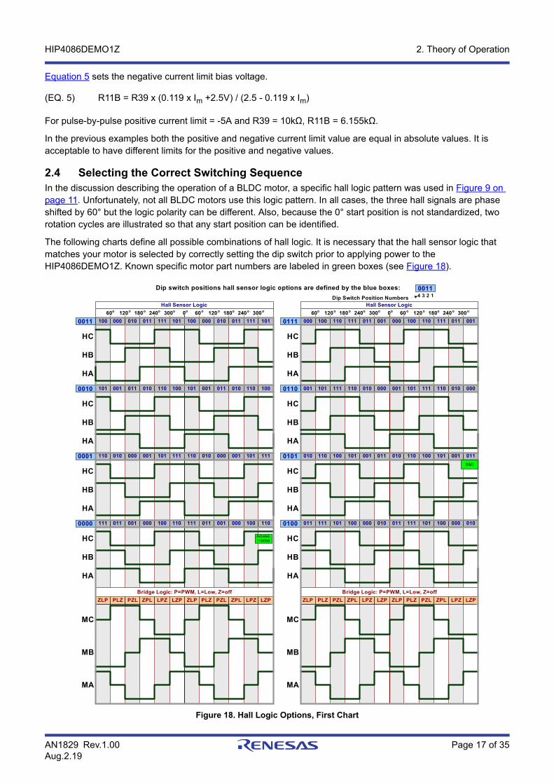
2.4 Selecting the Correct Switching SequenceIn the discussion describing the operation of a BLDC motor, a specific hall logic pattern was used in Figure 9 on page 11. Unfortunately, not all BLDC motors use this logic pattern. In all cases, the three hall signals are phase shifted by 60° but the logic polarity can be different. Also, because the 0° start position is not standardized, two rotation cycles are illustrated so that any start position can be identified.
The following charts define all possible combinations of hall logic. It is necessary that the hall sensor logic that matches your motor is selected by correctly setting the dip switch prior to applying power to the HIP4086DEMO1Z. Known specific motor part numbers are labeled in green boxes (see Figure 18).
Figure 18. Hall Logic Options, First Chart
R11B = R39 x (0.119 x Im +2.5V) / (2.5 - 0.119 x Im)(EQ. 5)
Hall Sensor Logic
ZLP PLZ PZL ZPL LPZ LZP ZLP PLZ PZL ZPL LPZ LZP
Bridge Logic: P=PWM, L=Low, Z=off
MB
MA
MC
HC
HB
HA
101 001 011 010 110 101 001 011 010 110100 100
HC
HB
HA
110 010 000 001 101 110 010 000 001 101111 111
HC
HB
HA
111 011 001 000 100 111 011 001 000 100110 110
0010
0001
0000
HC
HB
HA
100 000 010 011 111 100 000 010 011 111101 1010011
Ametek 119056
000 100 110 111 011 000 100 110 111 011001 001
Hall Sensor Logic
HC
HB
HA
HC
HB
HA
010 110 100 101 001 010 110 100 101 001011 011
HC
HB
HA
011 111 101 100 000 011 111 101 100 000010 010
0111
0101
0100
ZLP PLZ PZL ZPL LPZ LZP ZLP PLZ PZL ZPL LPZ LZP
Bridge Logic: P=PWM, L=Low, Z=off
MB
MA
MC
001 101 111 110 010 001 101 111 110 010000 000
HC
HB
HA
0110
B&D
Dip switch positions hall sensor logic options are defined by the blue boxes: 00114 3 2 1Dip Switch Position Numbers
300o240o180o120o60o 240o180o120o60o0o 300o 300o240o180o120o60o 240o180o120o60o0o 300o

HIP4086DEMO1Z 2. Theory of Operation
AN1829 Rev.1.00 Page 18 of 35Aug.2.19
Notice that the dip switch settings for these Hall sensor logic charts (Figure 19) are the same as Figure 18. This is not an error.
Figure 19. Hall Logic Options, Second Chart
001 011 111 110 100 001 011 111 110 100000 000
000 010 110 111 101 000 010 110 111 101001 001
010 000 100 101 111 010 000 100 101 111011 011
011 001 101 100 110 011 001 101 100 110010 010
LZP LPZ ZPL PZL PLZ ZLP LZP LPZ ZPL PZL PLZ ZLP
Bridge Logic: P=PWM, L=Low, Z=off
Bodine3304
HC
HB
HA
HC
HB
HA
HC
HB
HA
0101
0100
MB
MA
MC
HC
HB
HA
0110
LZP LPZ ZPL PZL PLZ ZLP LZP LPZ ZPL PZL PLZ ZLP
Bridge Logic: P=PWM, L=Low, Z=off
100 110 010 011 001 100 110 010 011 001101 101
111 101 001 000 010 111 101 001 000 010110 110
110 100 000 001 011 110 100 000 001 011111 111
101 111 011 010 000 101 111 011 010 000100 100
MB
MA
MC
HC
HB
HA
HC
HB
HA
HC
HB
HA
0010
0001
0000
HC
HB
HA
Hall Sensor Logic Hall Sensor Logic
Dip switch positions hall sensor logic options are defined by the blue boxes: 00114 3 2 1Dip Switch Position Numbers
300o240o180o120o60o 240o180o120o60o0o 300o 300o240o180o120o60o 240o180o120o60o0o 300o
0011 0111
HIP4086DEMO1Z 3. Board Layout
AN1829 Rev.1.00 Page 19 of 35Aug.2.19
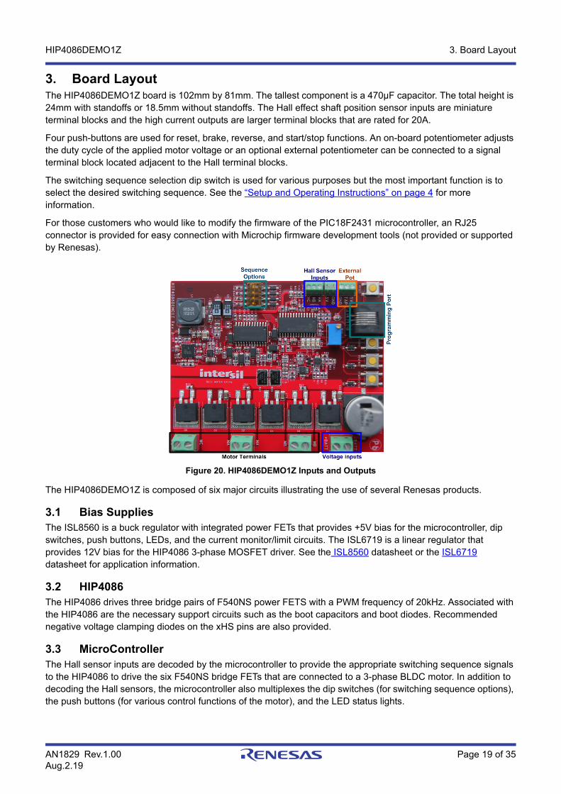
3. Board LayoutThe HIP4086DEMO1Z board is 102mm by 81mm. The tallest component is a 470µF capacitor. The total height is 24mm with standoffs or 18.5mm without standoffs. The Hall effect shaft position sensor inputs are miniature terminal blocks and the high current outputs are larger terminal blocks that are rated for 20A.
Four push-buttons are used for reset, brake, reverse, and start/stop functions. An on-board potentiometer adjusts the duty cycle of the applied motor voltage or an optional external potentiometer can be connected to a signal terminal block located adjacent to the Hall terminal blocks.
The switching sequence selection dip switch is used for various purposes but the most important function is to select the desired switching sequence. See the “Setup and Operating Instructions” on page 4 for more information.
For those customers who would like to modify the firmware of the PIC18F2431 microcontroller, an RJ25 connector is provided for easy connection with Microchip firmware development tools (not provided or supported by Renesas).
The HIP4086DEMO1Z is composed of six major circuits illustrating the use of several Renesas products.
3.1 Bias SuppliesThe ISL8560 is a buck regulator with integrated power FETs that provides +5V bias for the microcontroller, dip switches, push buttons, LEDs, and the current monitor/limit circuits. The ISL6719 is a linear regulator that provides 12V bias for the HIP4086 3-phase MOSFET driver. See the ISL8560 datasheet or the ISL6719 datasheet for application information.
3.2 HIP4086The HIP4086 drives three bridge pairs of F540NS power FETS with a PWM frequency of 20kHz. Associated with the HIP4086 are the necessary support circuits such as the boot capacitors and boot diodes. Recommended negative voltage clamping diodes on the xHS pins are also provided.
3.3 MicroControllerThe Hall sensor inputs are decoded by the microcontroller to provide the appropriate switching sequence signals to the HIP4086 to drive the six F540NS bridge FETs that are connected to a 3-phase BLDC motor. In addition to decoding the Hall sensors, the microcontroller also multiplexes the dip switches (for switching sequence options), the push buttons (for various control functions of the motor), and the LED status lights.
Figure 20. HIP4086DEMO1Z Inputs and Outputs

HIP4086DEMO1Z 3. Board Layout
AN1829 Rev.1.00 Page 20 of 35Aug.2.19
The on-board potentiometer (or an optional external pot) is monitored by the microcontroller to provide a duty cycle to the motor that is proportional to the tap voltage of the potentiometer and varies between 0% and 100% duty cycle. This proportional duty cycle is open loop and is independent of the bridge voltage. Consequently, any motor voltage between 15V and 60V can be used with this demo board.
The microcontroller firmware is provided as a reference but the only support offered by Renesas is for bug corrections and for adding more switching sequences. All firmware revisions for this demo board can be found on the website. The firmware revision of your demo board can be determined by referring to the “Test Mode Setup” on page 6.
3.4 Current Sensing/Current LimitTwo op-amps are used for current monitoring and current limiting. An ISL28134 low noise, low offset op-amp is configured as a differential amplifier for Kelvin connections across the current-sensing resistor. The diff-amp is also biased so that zero bridge current results with an output voltage that is 1/2 of the +5V bias. Consequently, positive bridge currents results with a current monitor signal that is greater than 2.5V (up to ~5V). Negative bridge currents (that occur with regenerative braking) is less than 2.5V (down to a minimum of ~0V). This ‘”bipolar” analog signal can be monitored by the microcontroller for purposes, such as torque control and/or regenerative braking.
The output of the analog differential amplifier is connected to two ISL28214 op-amps configured as outside window comparators for pulse-by pulse current limiting for either positive or negative current. The OR’ed comparator outputs are sent to the microcontroller for processing.
3.5 3-Phase BridgeThe 3-phase bridge is composed of six F540NS power MOSFETS (100V, 33A). Each FET is driven by one of the six driver outputs of the HIP4086. Dead time is provided by the controller (optionally, dead time can be provided by the HIP4086).
Figure 21. Major Circuit Locations
ISL6719(+12v)

HIP
40
86
DE
MO
1Z
3. Bo
ard Layo
ut
AN
182
9R
ev.1.00P
ag
e 21 o
f 35
Au
g.2
.19
3.6 Bill of Materials
Part Number Reference Designator Qty ValueTol.(%) Voltage Power
Package Type Jedec Type Manufacturer Description
10TPE330M C8, C9 2 330µF 10 10V SMD CAP_7343 SANYO-POSCAP
TPE SERIES LOW ESR PRODUCTS CAP
1725656 TB3 1 2MNT CON_TERM_MPT_2POS PHOENIX-CONTACT
100 Mil Micro-Pitch Terminal Block
1725669 TB1,TB2 2 3MNT CON_TERM_MPT_3POS PHOENIX-CONTACT
100 Mil Micro-Pitch Terminal Block
1729018 TB4-TB7 4 2 CON_TERM_MKDSN_2POS PHOENIX-CONTACT
200 Mil PCB Connector Terminal Block
1N4148W-7-F D2, D4, D8, D12-D15 7 SOD SOD123 DIODES Fast Switching Diode (RoHS COMPLIANT)
3299W-1-103-LF R13 1 10kΩ 10 1/2W RADIAL RES_POT_3299W BOURNS TRIMMER POTENTIOMETER (RoHS COMPLIANT)
555165-1 J2 1 6M2 CON_JACK_555165-1 TYCO Phone Jack Connector
597-3111-402 LED0-LED3 4 SMD DIA_LED1206 Dialight Surface Mount Red LED
B280 D1 1 SMD2 DIO_SMB DIODES 2A 80V SCHOTTKY BARRIER RECTIFIER
B3S-1002 BRAKE, RESET, REVERSE, START/STOP
4 SMD SW_B3S-1002 OMRON Momentary Pushbutton Tactile SMT Switch
BAT54A D3 1 COMMON-ANODE
SOT23 DIODES 30V SCHOTTKY DIODE
C0805C106K8PACTU C7, C10 2 10µF 10 10V 805 CAP_0805 KEMET MULTILAYER CAP
C1608X7R1C105K C16, C33, C47 3 1µF 10 16V 603 CAP_0603 TDK MULTILAYER CAP
C1608X7R1H104K C15 1 0.1µF 10 50V 603 CAP_0603 TDK MULTILAYER CAP
C3225X7R2A105M C5 1 1µF 20 100V 1210 CAP_1210 TDK Ceramic Chip Cap
CSTCE10M5G55 Y1 1 SMD CSTCE12M MURATA 10MHz CERALOCK Resonator
DR125-220-R L1 1 22.0µH 20 4.71A SMD IND_DR125 COOPER-BUSSMANN
High Power Density Shielded Inductor
EEVFK1K471M C27 1 470µF 20 80V SMD CAPAE_708X650 PANASONIC Aluminum Elect SMD Cap
ES1B D5-D7, D9-D11 6 DO214 DO214_AC FAIRCHILD 1A 150V Fast Rectifier Diode
GRM21BR71C475KA73L C42, C45, C46, C50 4 4.7µF 10 16V 805 CAP_0805 MURATA CERAMIC CAP

HIP
40
86
DE
MO
1Z
3. Bo
ard Layo
ut
AN
182
9R
ev.1.00P
ag
e 22 o
f 35
Au
g.2
.19 GENERIC C4 1 100PF 10 25V 603 CAP_0603 Various MULTILAYER CAP
GENERIC C23, C25 2 100PF 10 50V 603 CAP_0603 Various MULTILAYER CAP
GENERIC C14, C30, C41 3 0.01µF 10 50V 603 CAP_0603 Various Multilayer Cap
GENERIC C38, C40 2 0.1µF 10 25V 603 CAP_0603 Various Multilayer Cap
GENERIC C17 1 220pF 10 50V 603 CAP_0603 Various Multilayer Cap
GENERIC C35-C37 3 0.22µF 10 16V 603 CAP_0603 Various Multilayer Cap
GENERIC C24 1 390pF 10 50V 603 CAP_0603 Various Multilayer Cap
GENERIC C26 1 470pF 10 100V 603 CAP_0603 Various Multilayer Cap
GENERIC C32 1 470pF 10 50V 603 CAP_0603 Various Multilayer Cap
GENERIC C3, C49 2 4700pF 10 50V 603 CAP_0603 Various Multilayer Cap
GENERIC C6 1 0.047µF 10 25V 603 CAP_0603 Various Multilayer Cap
GENERIC C51 1 OPEN 5 OPEN 603 CAP_0603 Various Multilayer Cap
GENERIC C1, C2, C11 3 0.1µF 10 100V 805 CAP_0805 Various Multilayer Cap
GENERIC C29, C31, C34, C48 4 1µF 10 100V 1206 CAP_1206 Various Multilayer Cap
GENERIC R5, R34, R52, R61, R62
5 DNP 1 DNP 603 RES_0603 Various Metal Film Chip Resistor (Do Not Populate)
GENERIC RJ2, RJ3 2 DNP 0.10 DNP 603 RES_0603 Various Metal Film Chip Resistor (Do Not Populate)
GENERIC R19, R26, R27 ,R36, R37, R40
6 33 5 1/16W 603 RES_0603 Various Thick Film Chip Resistor
GENERIC RJ1 1 0 0 1/16W 603 RES_0603 Various Thick Film Chip Resistor
GENERIC R42, RJ4, RJ10, RJ11 4 0 1 1/16W 603 RES_0603 Various Thick Film Chip Resistor
GENERIC R46 1 100 1 1/16W 603 RES_0603 Various Thick Film Chip Resistor
GENERIC R47-R49, R51, R58-R60
7 1kΩ 1 1/16W 603 RES_0603 Various Thick Film Chip Resistor
GENERIC R16, R25, R28-R33, R35, R38 ,R39, R43-R45, R4, R11
16 10kΩ 1 1/16W 603 RES_0603 Various Thick Film Chip Resistor
GENERIC R12A, R12B 2 1MΩ 1 1/16W 603 RES_0603 Various Thick Film Chip Resistor
GENERIC R1, R11B 2 249Ω 1 1/16W 603 RES_0603 Various Thick Film Chip Resistor
GENERIC R10 1 16.2kΩ 1 1/16W 603 RES_0603 Various Thick Film Chip Resistor
Part Number Reference Designator Qty ValueTol.(%) Voltage Power
Package Type Jedec Type Manufacturer Description

HIP
40
86
DE
MO
1Z
3. Bo
ard Layo
ut
AN
182
9R
ev.1.00P
ag
e 23 o
f 35
Au
g.2
.19 GENERIC R20 1 2kΩ 1 1/16W 603 RES_0603 Various Thick Film Chip Resistor
GENERIC R7, R53-R55 4 20kΩ 1 1/16W 603 RES_0603 Various Thick Film Chip Resistor
GENERIC R6 1 301kΩ 1 1/16W 603 RES_0603 Various Thick Film Chip Resistor
GENERIC R3, R12, R14, R15 4 32.4kΩ 1 1/16W 603 RES_0603 Various Thick Film Chip Resistor
GENERIC R41 1 470Ω 1 1/16W 603 RES_0603 Various Thick Film Chip Resistor
GENERIC R17, R18, R21, R22 4 511Ω 1 1/16W 603 RES_0603 Various Thick Film Chip Resistor
GENERIC R9 1 51.1kΩ 1 1/16W 603 RES_0603 Various Thick Film Chip Resistor
GENERIC R8 1 5.62kΩ 1 1/16W 603 RES_0603 Various Thick Film Chip Resistor
GENERIC R50 1 7.15kΩ 1 1/16W 603 RES_0603 Various Thick Film Chip Resistor
GENERIC R2, R56, R57 3 1.2Ω 1 1/8W 1206 RES_1206 Various Thick Film Chip Resistor
HIP4086ABZ U5 1 SOIC SOIC24_300_50 Renesas Three Phasre Driver 80v 0.5A
IRFS4710 Q1-Q6 6 D2PAK D2PAK IR N-Channel 100V 75A HEXFET Power MOSFET
ISL28134IBZ (Note 1) U2 2 SOIC8 SOIC8_150_50E Renesas Single 5V Ultra Low Noise Zero Drift Rail-to-Rail Precision Operational Amplifier
ISL28214FUZ (Note 1) U3 2 MSOP MSOP8_118_256 Renesas Dual General Purpose Micropower RRIO Op Amp
ISL6719ARZ U6 1 DFN DFN9_118X118_197_EP Renesas 100V Linear Regulator
ISL8560IRZ U1 1 20QFN QFN20_236X236_315_EP Renesas 2A DC/DC POWER SWITCHING REGULATOR
PIC18F2431S0 U4 1 SOIC SOIC28_300_50V2 Microchip Flash Microcontroller
SD04H0SK SW1 1 SMT SD04H0SK C&K SD Series Low Profile DIP Switch 4 Pos SPST
WSH2818R0150FE R23, R24 2 0.015Ω 1 5W 2818 RES_WSH2818 VISHAY SURFACE MOUNT POWER METAL STRIP RESISTOR
TOTAL 157
Note: 1. On previous board revisions U2 and U3 are the ISL28246.
Part Number Reference Designator Qty ValueTol.(%) Voltage Power
Package Type Jedec Type Manufacturer Description

HIP
40
86
DE
MO
1Z
3. Bo
ard Layo
ut
AN
182
9R
ev.1.00P
ag
e 24 o
f 35
Au
g.2
.19
3.7 HIP4086DEMO1Z Board Schematics
Figure 22. Bias Supplies
BIAS SUPPLIES
IN
OUT
OUT
C15
0.1U
F
50V
C48
1UF
16.2
K
0603
R10
C47
1UF
R52
DN
P06
03
C11
0.1U
F
100V
R9
51.1
K
0603
220P
F
C17
OP
EN
0603
C51
C16
1UF
16V
10U
F
C7
EP
U1
ISL8560IRZ
1 LX
2 LX
3 BOOT
4 EN
5 VCC5
6S
YN
C
7R
TC
T
8S
GN
D
9F
B
10C
OM
P
11REF
12PGOOD
13PGND
14SS
15LX
16LX
17V
IN
18V
IN
19V
IN
20V
IN
21
0
RJ11
D1
B28
0
12
RJ10
0
10U
F
C10
100V1U
F
C5
DR125-220-R
22.0UH
L11 2
R7
20K0603
C8
330U
F
12
R6
0603301K
50V
100P
F
C25
1KR51
C23
50V100PF
EP
AUXIN
COMPB
ENABLE
COMPA VSW_FB
VSW
ENABLE_N
GND VPWR
ISL6719ARZ
U6 1
2
3
45
6
7
8
9
10
0603
5.62
K
R8
7.15
K
R50
C9
330U
F
12
C14
0.01UF50V
C1
0.1U
F
100V
R42
0
100V
470P
F
C26
C24
50V390PF
0.1U
F
C2
UNNAMED_2_ISL6719_I129_1
UNNAMED_2_ISL6719_I129_3
UNNAMED_2_ISL6719_I129_4UNNAMED_2_ISL6719_I129_5
UNNAMED_2_ISL6719_I129_6
UNNAMED_2_ISL8560_I164_11
UNNAMED_2_ISL8560_I164_14
UNNAMED_2_ISL8560_I164_3
UNNAMED_2_ISL8560_I164_5
UNNAMED_2_SHIELDEDIND_I21_A UNNAMED_2_SHIELDEDIND_I21_B
UNNAMED_2_SMCAP_I12_B
UNNAMED_2_SMCAP_I17_B
UN
NA
ME
D_
2_
SM
CA
P_
I26
_A
UNNAMED_2_SMCAP_I26_B
UN
NA
ME
D_
2_
SM
CA
P_
I27
_A
UNNAMED_2_SMCAP_I30_B
V_12V
V_48V
V_5V

HIP
40
86
DE
MO
1Z
3. Bo
ard Layo
ut
AN
182
9R
ev.1.00P
ag
e 25 o
f 35
Au
g.2
.19
Figure 23. Controller
DRAWN BY: DATE: DATE:ENGINEER:
TIM KLEMANN TIM LOC
MICROCONTROLLER
PORTPROGRAMING
HALL SWITCHES
+5V
GND
EXTERNALCONTROLSPEED
(OPTIONAL)POTENTIOMETER
HALL BIAS
CONTROLLER
BA
C
IN
IN
IN
OUT
OUT
OUT
OUT IN
IN
OUT
OUT
OUT
OUT
OUT
OUT
OUT
IN
IN
10K
R30
1
RE
VE
RS
E1 2
34
1K
R58
2
D12 1
2
10K
R32
50V
0.01
UF
C30
2
1K
R59
10K
R43
TB2-3
1
D13 1
2
10K
R28
3
4.7U
F
C42
LED
0
12
D2
12
3
PIC18F2431S0
U4
1 MCLR
2 RA03 RA1
4 RA2
5 RA3
6 RA4
7 AVDD
8 AVSS
9 OSC1
10 OSC2
11 RC0
12 RC1
13 RC2
14 RC3 15RC4
16RC5
17RC6
18RC7
19VSS
20VDD
21RB0
22RB1
23RB2
24RB3
25RB4
26RB5
27RB6
28RB7
10K
R33
4
10K
R16
1K
R60
ST
AR
T/S
TO
P 1 234
2
D14 1
2
4.7U
F
C45
5
10K
R45
4.7U
F
C50
0
RJ1
RE
SE
T
1 234
TB1-3
1
21 43
5678
SW
1
1 2 3 45678
470
R41
555165-1
J2-1
6
D8
12
LED
1
12
10K
R29
10M
HZ
CS
TC
E10
M5G
55Y1
1
2
3
D15 1
2
100P
F
C4
1
BR
AK
E1 2
34
10K
R31
LED
2
12
10K
R44
1K
R48
10K
R25
TB3-2
2
2K
R20
LED
3
12
0.04
7UF
C6
D4
12
1K
R49
4.7U
F
C46
3
10K
R35
10K R
131
2
3
/FLTA
IMOT
MCLR
MCLR
PWM0
PWM1
PWM2
PWM3
PWM4
PWM5
RB6
RB6
RB7
RB7
UNNAMED_3_B3S_I112_1
UN
NA
ME
D_
3_
B3
S_
I17
_2
UN
NA
ME
D_
3_
B3
S_
I18
_2
UNNAMED_3_B3S_I18_3
UN
NA
ME
D_
3_
B3
S_
I39
_2
UNNAMED_3_B3S_I39_3
UNNAMED_3_CSTCE10M_I164_P1
UNNAMED_3_CSTCE10M_I164_P3
UNNAMED_3_PIC18F2431_I92_11
UNNAMED_3_PIC18F2431_I92_13
UNNAMED_3_PIC18F2431_I92_14 UNNAMED_3_PIC18F2431_I92_15
UNNAMED_3_PIC18F2431_I92_16
UNNAMED_3_PIC18F2431_I92_17
UNNAMED_3_PIC18F2431_I92_18
UNNAMED_3_PIC18F2431_I92_2
UNNAMED_3_PIC18F2431_I92_3
UNNAMED_3_PIC18F2431_I92_4
UNNAMED_3_PIC18F2431_I92_5
UNNAMED_3_PIC18F2431_I92_6
UNNAMED_3_SD04H0SK_I176_PIN4
UNNAMED_3_SD04H0SK_I176_PIN5UNNAMED_3_SD04H0SK_I176_PIN6UNNAMED_3_SD04H0SK_I176_PIN7UNNAMED_3_SD04H0SK_I176_PIN8
UNNAMED_3_SMCAP_I35_A
UNNAMED_3_SMLED_I108_A
UNNAMED_3_SMRES_I111_A
UNNAMED_3_SMRES_I186_A
UNNAMED_3_SMRES_I187_A
UNNAMED_3_SMRES_I3_B
V_5V
V_5V
V_5V
V_5V

HIP
40
86
DE
MO
1Z
3. Bo
ard Layo
ut
AN
182
9R
ev.1.00P
ag
e 26 o
f 35
Au
g.2
.19
Figure 24. Bridge and Current Sense
RELEASED BY:
DRAWN BY: DATE:
DATE:
DATE:
ENGINEER:
TITLE:
UPDATED BY:
06/27/2019
TIM KLEMANN
DEMO
DRIVER WHILE TROUBLE-
RJ3 = O OHM
SHOOTING CODE.
TO DISABLE BRIDGE
3 PHASE BRAND CURREN
RJ5= OPEN, R5=10K...100K.
FOR DEAD TIME DELAYS:
RJ5= 0 OHM, R5 = OPEN.
FOR NO DEAD TIME DELAYS:
IN
IN
OUT
IN
IN
IN
IN
IN
IN
OUT
OUT
OUT
OUT
OUT
OUT
OUT
IN
IN
IN
IN
IN
IN
IN
R61
DN
PR21
511
D3
1
23
V+
OUT
V-U2ISL28134IBZ
2
3
4
6
7
R4033
RJ3
DNP
C31
1UF
C27
470U
F1
2
R62
DN
P
C35
0.22
UF
Q6IRFS4710
1
23
R12A
1M
D9
12
R3733
R47 1K
D7
12
C29
1UF
R2
1.2
VDD
VSS
ALO
BLO
RFSH
CLI
BHOBHB
/AHI
/CHI
UVLO
RDEL
CLO
AHS
AHO
AHB
CHS
CHO
CHB
DIS
BHS
ALI
BLI
/BHI
U5
HIP4086ABZ
1
2
3
4
5
6
7
8
9
10
11
12 13
14
15
16
17
18
19
20
21
22
23
24
C37
0.22
UF
Q5IRFS4710
1
23
C40
0.1U
F
D11
12
R3633
2
1
R57
1.2
C331UF
Q4IRFS4710
1
23
R12B
1M
D10
12
R2733
TB7-31
TB4-2
2
OUTU3B
ISL28214FUZ
5
67
R56
1.2
C36
0.22
UF
Q3IRFS4710
1
23
C32470PF
C41
50V
0.01
UF
R23
0.01
51
2
RJ4 0
1
4700
PF
C49
R11
B
133
D6
12
Q2IRFS4710
1
23
R3
32.4
K
U3AISL28214FUZ
12
3
48
C3
4700
PF
R55
20K
R5
DN
P
R15
32.4K
TB6-2
2
R39
10K
Q1IRFS4710
1
23
R4
10K
R54
20K
DN
P
R34
R14
32.4K
2
R38
10K
R2633
C38
0.1U
F
R24
0.01
5
12
R18
511R11
10K
R22
511
R46
100
R53
20K
RJ2
DN
P
R12
32.4K
TB5-3
1
R1
133
R1933
D5
12
C34
1UF
R17
511
/FLTA
AHO
AHO
ALO
ALO
BHOBHO
BLOBLO
CHO
CHO
CLO
CLO
GND_CSIMOT
MA
MB
MC
PWM0
PWM1
PWM2
PWM3
PWM4
PWM5
UNNAMED_1_ES1AD_I100_CAT
UNNAMED_1_ES1AD_I113_CAT
UNNAMED_1_ES1AD_I115_CAT
UNNAMED_1_HIP4086_I1_AHB
UNNAMED_1_HIP4086_I1_BHB
UNNAMED_1_HIP4086_I1_CHB
UNNAMED_1_HIP4086_I1_DIS
UNNAMED_1_HIP4086_I1_RDEL
UNNAMED_1_HIP4086_I1_RFSH
UNNAMED_1_HIP4086_I1_UVLO
UNNAMED_1_IRFS4710_I197_G
UNNAMED_1_IRFS4710_I198_G
UNNAMED_1_IRFS4710_I199_G
UNNAMED_1_IRFS4710_I200_G
UNNAMED_1_IRFS4710_I201_G
UNNAMED_1_IRFS4710_I202_G
UNNAMED_1_ISL28134_I319_IN
UNNAMED_1_ISL28134_I319_IN_1
UNNAMED_1_ISL28134_I319_OUT
UNNAMED_1_ISL28214_I320_NIN
UNNAMED_1_ISL28214_I320_OUT
UNNAMED_1_ISL28214_I320_PIN
UNNAMED_1_ISL28214_I321_OUT
UNNAMED_1_ISL28214_I321_PIN
UNNAMED_1_SMCAP_I123_B
UNNAMED_1_SMCAP_I125_A
UNNAMED_1_SMRES_I282_B
V_12V
V_48V
V_5V
V_5V

HIP4086DEMO1Z 3. Board Layout
AN1829 Rev.1.00 Page 27 of 35Aug.2.19
3.8 PCB Layout
Figure 25. Assembly Top

HIP4086DEMO1Z 3. Board Layout
AN1829 Rev.1.00 Page 28 of 35Aug.2.19
Figure 26. Silkscreen Top

HIP4086DEMO1Z 3. Board Layout
AN1829 Rev.1.00 Page 29 of 35Aug.2.19
Figure 27. Top Layer

HIP4086DEMO1Z 3. Board Layout
AN1829 Rev.1.00 Page 30 of 35Aug.2.19
Figure 28. Layer 2

HIP4086DEMO1Z 3. Board Layout
AN1829 Rev.1.00 Page 31 of 35Aug.2.19
Figure 29. Layer 3

HIP4086DEMO1Z 3. Board Layout
AN1829 Rev.1.00 Page 32 of 35Aug.2.19
Figure 30. Bottom Layer

HIP4086DEMO1Z 4. Revision History
AN1829 Rev.1.00 Page 33 of 35Aug.2.19
4. Revision History
Rev. Date Description
1.00 Aug.2.19 Applied new formatting throughout document.Updated Figure 1 on page 3.Updated Figures 15 and 16 on page 15.Updated Figure 17 on page 16.Updated the Current Sensing/Current Limit section on page 21.Updated schematics and BOM.Updated Figures 25-30.Updated disclaimer.
0.00 May.31.19 Initial release

Corporate HeadquartersTOYOSU FORESIA, 3-2-24 Toyosu,Koto-ku, Tokyo 135-0061, Japanwww.renesas.com
Contact InformationFor further information on a product, technology, the most up-to-date version of a document, or your nearest sales office, please visit:
www.renesas.com/contact/
TrademarksRenesas and the Renesas logo are trademarks of Renesas Electronics Corporation. All trademarks and registered trademarks are the property of their respective owners.

HIP4086DEMO1Z
AN1829
Renesas Electronics Corporationwww.renesas.com