university of nairobi department of physics
TRANSCRIPT

UNIVERSITY OF NAIROBI
DEPARTMENT OF PHYSICS
Fabrication and Characterization of TiO2/Nb2O5 Composite Photo-Electrodes
Deposited Using Electrophoretic Technique for Application in Dye-Sensitized
Solar Cells
John Njagi Nguu
I80/82761/2012
Department of Physics
University of Nairobi
Kenya.
A Thesis Submitted in Fulfillment of the Requirements for Award of the Degree of Doctor
of Philosophy in Physics of the University of Nairobi
December 2017

ii
DECLARATION

iii
DEDICATION
I dedicate this thesis to my beloved wife Susan Mumbua and our children Victor, Nicholus
and Joyesther who stood by me and encouraged me during the study.

iv
ACKNOWLEDGEMENTS
I would like to thank our heavenly Father for giving me the ability and resources that enabled
me study and complete my PhD studies.
Special thanks to my University advisors Prof. B. O. Aduda, Dr. F. W. Nyongesa, and Dr. R.
J. Musembi for their guidance and advice during the course of this study. I acknowledge
support of members of Department of Physics, University of Nairobi (UON) especially those
in the Condensed Matter Group.
I am very thankful to Daystar University management board for allocating me a reduced
workload and awarding me a scholarship to cover the tuition for my studies at the University
of Nairobi. I am indebted to my Daystar University colleagues for moral support through the
course of this study.
Special acknowledgement is to the National Commission for Science, Technology and
Innovation (NACOSTI) and International Programme in Physical Sciences (IPPS) for
financially supporting the sourcing of the chemicals, equipment, and materials used in this
work. I thank the management at Chuka University (Kenya) for allowing me use the Hall
Effect apparatus. I am grateful to Henry Barasa and Frandsen of the Joint United States
Africa Materials Initiative (JUAMI) for facilitating my use of both the SEM and XRD.

v
ABSTRACT
This study has investigated a rapid, simple and cost effective electrophoretic deposition
(EPD) technique for fabrication of nanoparticulate TiO2/Nb2O5 composite electrode films for
use in dye-sensitized solar cells (DSSCs). The EPD technique parameters were categorized
into suspension-related and process-related parameters. The suspension-related parameters
were maintained constant by fixing the solvent (2-propanol), charging system
(Mg(NO3)2.6H2O), pH (≈ 4.9) of suspension and EPD apparatus. The optimized process-
related parameters of EPD technique obtained were: particle concentration (0.25 g/L), DC
applied voltage (35V), and deposition time (90s). The optical properties like light absorption,
transmission, extinction coefficient, Urbach energy, refractive index, and optical band gap
energy of the composite thin films were investigated in this study. Band gap energies ( gE )
for pure TiO2, (3.932 eV), pure Nb2O5 (3.858 eV) and TiO2/Nb2O5 composite films
(3.884eV) were obtained based on the plot of the Tauc equation. The theoretical gE of TiO2
is =3.25 eV and gE =3.49 eV for Nb2O5. The difference between theoretical and
experimental values of gE for both pure TiO2 and Nb2O5 films was explained in terms of
development of sub-band gap states lying deep in the tail of density of states in the
TiO2/Nb2O5 composite films. The band gap decreased slightly from 3.8911eV for films
annealed at 450°C for 1 hour to 3.7965 eV for similar films annealed at same temperature for
6 hours. The narrowing of band gap was attributed to the decrease in transitions due to
reduction of the oxygen defect width as a result of air annealing which fills up the vacant
oxygen levels.
Light is absorbed in a material when extinction coefficient ( k ) is greater than zero i.e.,
k > 0, while light travels straight through the material when k = 0. In this study, a value of
0.0354 at 400 ≤ λ ≤ 700nm was obtained for extinction coefficient which means there was
some absorption of light by the TiO2/Nb2O5 composite electrode thin films due to their large
band gap energy. The results were consistent with the knowledge about high band gap
semiconductors that must require sensitization with a dye to function as photoelectrodes in a
dye sensitized solar cells.. The relatively small extinction coefficient was attributed to low
absorption of light by the TiO2/Nb2O5 composite electrode thin film due to its large energy
band gap. The calculations of Urbach energy ( UE ) yielded a value equal to 454 meV, which

vi
indicated substantial introduction of tail states at the band edges that influence the electron
transport. The average refractive index (n) of 1.643 was obtained for wavelengths between
1800nm and 2800nm.
The majority carriers in the TiO2/Nb2O5 composite films were found to be electrons (n-type)
which could be caused by caused by incorporation of Nb+5, and O-2 ions in the composite.
Charge carrier density ( dn ) value for TiO2/Nb2O5 composite films were 6.14 x 1018 cm-3
which was lower than the value (1.00 x 1019 cm-3) reported in existing research. This was
attributed to electrons trapping in surface states of the high surface area composite film while
reduction of carrier mobility could have resulted from increased grain boundaries between the
Nb2O5 and TiO2 nanoparticles in a composite film. The SEM images showed the TiO2/Nb2O5
composite films were devoid of cracks and essential for dye adsorption. Both TiO2 and
Nb2O5 nanoparticles were shown, by XRD graphs, to be presented in the composite films in
the ratio 1.78:1 (or 1:0.56). The XRD graphs confirmed that surface of both TiO2 and Nb2O5
particles suspended in 2-propanol became charged and therefore the charged particles were
moved and deposited on oppositely charged electrode by the applied electric field. The XRD
revealed dominant peak of TiO2 at 2θ = 25.5° and that of Nb2O5 at 2θ = 26.5°. Applying
Scherer’s equation, the average crystallite sizes at these peak positions were 15.36 nm and
15.49 nm and hence the crystallite dimensions were confirmed to the nanoscale.
The solar cell produced using the composite thin film had the following parameters: VOC =
0.66V, JSC = 5.25 mA/cm2, FF = 0.57, and = 2. The low conversion efficiency observed
was accredited to factors such as composition of the composite, morphological defects, poor
adhesion between film and FTO, or the type of dye used. Nonetheless, efficiencies in these
types of devices where the electrode is deposited by EPD has remained low. Internal
resistances were investigated by EIS measurements to explain the low cell efficiencies. All
the cells exhibited the Gerischer impedance (RD) characterized by Nyquist plot having a
single, main arc in which impedance was associated with the electron recombination with
electrolyte species being faster than the transport of electron within the TiO2 film. The faster
back reaction could have been caused by the relatively poor adhesion of the film on to FTO
glass slides. The poor adhesion introduced high transport resistance and low interfacial
(recombination) resistances. Blocking the electron leak by structural modification that
includes developing a more compact composite structure and improved film/FTO glass

vii
adherence that enhances electron conduction across the interface may be a possible way to
obtain high JSC s and efficiencies in DSSCs.
Key words: Dye-sensitized solar cell, electrophoretic deposition, niobium (v) oxide,
TiO2/Nb2O5 composite electrode thin film, electrochemical impedance spectroscopy.
viii
TABLE OF CONTENTS
1.1 Background ......................................................................................................... 1
1.2 Problem Statement .............................................................................................. 8
1.3 Aim of the Study ................................................................................................. 9
1.4 Justification and Significance of the Study ........................................................ 9
2.1 DSSC Structure ................................................................................................. 11
2.2 Techniques for Fabricating DSSC Photoelectrode ........................................... 12
2.3 Factors Affecting Efficiency of DSSCs ............................................................ 18
2.4 Electrophoretic Deposition (EPD) and Factors Affecting Film Deposition ..... 22
2.5 Electrochemical Impedance Spectroscopy Characterization of DSSC ............ 30
3.1 The Working Principle of a Dye-Sensitized Solar Cell (DSSC) ...................... 32
3.2 Solar Radiation and Materials for Solar Cells .................................................. 37
3.3 Possible Film Structures from EPD Deposition ............................................... 38
3.3.1 Theory of electrophoretic deposition (EPD) of photoanode ................ 42
3.3.2 Factors influencing EPD ...................................................................... 43
3.4 Optical Characterization of Deposited Films ................................................... 47
3.5 Electrical Characterization ............................................................................... 53
3.5.1 The Hall Effect ..................................................................................... 54
3.6 Structural Characterization ............................................................................... 57
3.7 Characterization of DSSCs ............................................................................... 59
3.8 Electrochemical Impedance Spectroscopy ....................................................... 62
DECLARATION ..................................................................................................................... ii
DEDICATION ........................................................................................................................ iii
ACKNOWLEDGEMENTS .................................................................................................... iv
ABSTRACT ............................................................................................................................. v
TABLE OF CONTENTS ...................................................................................................... viii
LIST OF TABLES .................................................................................................................. xi
LIST OF FIGURES ............................................................................................................... xii
LIST OF SYMBOLS, ABBREVIATIONS, AND ACRONYMS ........................................ xv
CHAPTER ONE INTRODUCTION ................................................................................... 1
CHAPTER TWO LITERATURE REVIEW ...................................................................... 11
CHAPTER THREE THEORETICAL FRAMEWORK .................................................... 32

ix
4.0 Introduction ...................................................................................................... 72
4.1 Preparation of Transparent and Electrical Conducting Electrode .................... 72
4.2 Preparation of the EPD Suspension .................................................................. 72
4.3 Electrophoretic Deposition of the TiO2/Nb2O5 Composite Films .................... 73
4.4 Determination of optimum mixing ratio of Nb2O5 and TiO2 for Film
Formation .......................................................................................................... 74
4.5 Optimization of Particle Concentration in EPD Suspension ............................ 75
4.6 Optimization of DC Applied Voltage for EPD ................................................ 75
4.7 Optimization of Deposition Time for EPD ....................................................... 75
4.8 Measurement of Film Thickness ...................................................................... 76
4.9 Characterization of TiO2/Nb2O5 Composite Films Deposited by EPD
Technique ......................................................................................................... 76
4.10 Optical Characterization ................................................................................... 76
4.11 Electrical Characterization ............................................................................... 77
4.12 Morphological Characterization ....................................................................... 78
4.13 Structural Analysis ........................................................................................... 79
4.14 Preparation of Components and Assembly of DSSCl ...................................... 79
4.15 Current-Voltage (I-V) Characterization of DSSC ............................................. 82
4.16 Electrochemical Impedance Spectroscopy (EIS) Measurement of DSSC ....... 82
5.0 The pH and Optimization of Ratios of TiO2 and Nb2O5 Particles in
Suspension ........................................................................................................ 85
5.1 Optimization of Concentration of TiO2 and Nb2O5 Particles in Suspension .... 87
5.2 The Optimization of Deposition Time .............................................................. 89
5.3 Optimization of Applied Voltage ..................................................................... 91
5.4 Morphological Characterization of TiO2/Nb2O5 Composite Electrode Thin
Films Using Scanning Electron Microscope (SEM) ........................................ 93
5.5 Structural Characterization of TiO2/Nb2O5 Composite Electrode Thin
Films Using X-Ray Diffraction Analyzer ........................................................ 95
5.6 Evaluation of Optical Band Gap Energy (Eg) of TiO2/Nb2O5 Composite
Films ................................................................................................................. 97
5.7 Effect of Annealing Time on Optical Band Gap of Composite Films ............. 99
CHAPTER FOUR MATERIALS AND METHODS ......................................................... 72
CHAPTER FIVE RESULTS AND DISCUSSION ............................................................ 85

x
5.8 Evaluation of Urbach Energy ......................................................................... 101
5.9 Extinction Coefficient ..................................................................................... 102
5.10 Evaluation of Refractive Index ( n ) ............................................................... 104
5.11 The Polarity of Charge Carriers ...................................................................... 105
5.12 Charge Carrier Density and Carrier Mobility ................................................. 107
5.13 Characterization of a Complete Solar Cell by Measuring Photoelectric
Current-Voltage (I-V) Parameters .................................................................. 108
5.14 Characterization of a Complete Solar Cell by Measuring Electrochemical
Impedance Spectroscopy (EIS) ...................................................................... 109
5.15 Influence of the Electrophoretic Deposition Time on DSSC Cell Efficiency 113
5.16 Influence of Particle Concentration on DSSC Efficiency .............................. 115
5.17 Influence of EPD Applied Voltage on DSSC Efficiency ............................... 117
6.0 Conclusion ...................................................................................................... 120
6.1 Suggestions for Further Work ........................................................................ 122
CHAPTER SIX CONCLUSIONS AND RECOMMENDATIONS .............................. 120
REFERENCES .................................................................................................................... 123
APPENDIX A: XRD JPDS card no. 74-1940 TiO2 .................................................... 139
APPENDIX B: XRD JPDS card no. 28-0317 Nb2O5.................................................... 141
APPENDIX C: PUBLISHED PAPER I ........................................................................ 142
APPENDIX D: PUBLISHED PAPER II ...................................................................... 143
APPENDIX E: PUBLISHED PAPER III ..................................................................... 144

xi
LIST OF TABLES
Table 1.1: World primary energy utilization (consumption) by fuel in million tonnes
oil equivalent (Mtoe) ................................................................................................ 1
Table 1.2: Greenhouse gases: gas concentration, global warming potential (GWP) and
lifetime ..................................................................................................................... 2
Table 1.3: World record solar cell efficiencies for laboratory and research devices
reported by National Renewable Energy Laboratory ............................................... 6
Table 1.4: Photovoltaic performances of DSSCs using composites, doped and core-
shell photoelectrodes. ............................................................................................... 7
Table 2.1: Summary of electrophoretically deposited TiO2 based films applied to dye-
sensitized solar cells. .............................................................................................. 24
Table 3.2: The description of elements of the equivalent circuit of Transmission line
(TL) model ............................................................................................................. 68
Table 5.1: Optimized electrophoretic deposition (EPD) process parameters for
TiO2/Nb2O5 composite electrode films deposition. ................................................. 93
Table 5.2: Values of direct and indirect optical band gaps of TiO2 and Nb2O5 reported
by various authors. ................................................................................................. 98
Table 5.3: Band gap energies for TiO2/Nb2O5 composite films annealed at 450°C for
different annealing times between 1 and 6 hours. ................................................ 100
Table 5.4: Hall Effect parameters from the study compared to those reported by several
authors. ................................................................................................................. 108
Table 5.5: Values of equivalent circuit model elements (EIS) compared with Rs and Rsh
(I-V) for DSSCs based on TiO2/Nb2O5 composite photoelectrodes deposited
by EPD method .................................................................................................... 112
Table 5.6: Solar cell characteristics of DSSCs using TiO2/Nb2O5 composite electrode
films deposited at varying EPD deposition time .................................................. 115
Table 5.7: Solar cell characteristics of DSSCs using TiO2/Nb2O5 composite electrode
thin films deposited from varying EPD particle concentration ............................ 116
Table 5.8: Solar cell characteristics of DSSCs using TiO2/Nb2O5 composite electrode
thin films deposited by varying EPD applied voltage .......................................... 119
Table 5.9: Characteristics of DSSCs whose photoelectrode films were deposited using
electrophoretic technique as reported by several authors. ................................... 119

xii
LIST OF FIGURES
Figure 1.1: NASA Map of the world solar energy potential ...................................................... 3
Figure 1.2: Record research-solar cell efficiencies reported by National Renewable
Energy Laboratory (NREL) ..................................................................................... 5
Figure 2.1: Basic structure of a dye-sensitized solar cell ......................................................... 11
Figure 2.2: Schematic of diagram of screen printing process .................................................. 13
Figure 2.3: Schematic drawing of the EPD setup showing cathodic deposition of
charged particles of mixed metal oxides. ............................................................... 22
Figure 2.4: Typical deposit mass versus particle concentration .............................................. 25
Figure 2.5: Typical TiO2 thickness versus deposition time of BNT electrophoresis ............... 29
Figure 2.6: Typical experimental impedance spectra for DSSC with an ionic liquid
based electrolyte ..................................................................................................... 31
Figure 3.1: Schematic diagram of the working principle of a dye sensitized solar cell. ......... 32
Figure 3.2: The charge transfer kinetics and associated timescales (rates) in DSSC .............. 33
Figure 3.3: Spectral irradiance against wavelength requirement for solar cell materials. ....... 38
Figure 3.4: Possible film structures of two-particle EPD deposition (a) Core-shell
structures (b) mixed particles structure and (c) layered structures. ....................... 39
Figure 3.5: The molecular structure of cis-bis(isothiocyanato)bis(2,2'-bipyridyl-4,4'-
dicarboxylato)-ruthenium(II) bis-tetrabutylammonium [Dye N719] ..................... 40
Figure 3.6: Schematic drawing of the EPD setup showing cathodic deposition of
charged particles of mixed metal oxides. ............................................................... 43
Figure 3.7 Schematic of the electrical diffuse layer at the surface of a particle
suspended in solvent and the potential distribution across the double layer .......... 45
Figure 3.8: Typical variation of Zeta potential of TiO2 nanoparticles as a function of
pH for different concentrations of Zn(NO3)2 ......................................................... 46
Figure 3.9: Typical transmission of radiation through a film and substrate. Also shown
are the sources of attenuation of incident light including reflection,
scattering and absorption of the light. .................................................................... 48
Figure 3.10: Arrangement for measuring the Hall voltage showing current in x-
direction, magnetic field in y- direction and Hall voltage measured in z-
direction .................................................................................................................. 55
Figure 3.11: Typical graph of solar cell’s output current (solid line) and power (dashed
line) as function of voltage. .................................................................................... 61
Figure 3.12: A typical Nyquist plot and Bode plots resulting from projection onto /// ZZ plane and //Z plane for electrochemical system .......................... 64

xiii
Figure 3.13: Equivalent circuit of Transmission line (TL) model used to fit impedance
spectra of dye-sensitized solar cells ....................................................................... 67
Figure 3.14: Characteristic Nyquist plot measured on a liquid electrolyte based DSSC ......... 71
Figure 4.1: A schematic drawing of the EPD setup showing the two FTO coated glass
slides partially immersed into TiO2/Nb2O5_2-propanol suspension in a
beaker. .................................................................................................................... 73
Figure 4.2: Schematic drawing of Hall Effect measurement showing meters that
provide current and magnetic fields ....................................................................... 77
Figure 4.3: Functional block diagram of SRM-232 four point probe showing four
probes: inner two for measuring voltage and outer two for measuring
current. ................................................................................................................... 78
Figure 4.4: Schematic diagram of assembled dye-sensitized solar cell employing
TiO2/Nb2O5 composite electrode film. ................................................................... 81
Figure 4.5: Photograph of the assembled dye-sensitized solar cell based on
TiO2/Nb2O5 composite electrode film .................................................................... 81
Figure 4.6: Electrochemical impedance spectroscopy measurement set up ............................ 83
Figure 5.1: Hall coefficient versus proportion of Nb2O5 by mass in suspension..................... 86
Figure 5.2: (a) Variation of transmittance with wavelength, (b) variation of peak
transmittance with particle concentration and (c) film thickness versus
concentration for TiO2/Nb2O5 composite films deposited by EPD technique ....... 87
Figure 5.3: (a) Variation of transmittance with wavelength, (b) variation of peak
transmittance with deposition time and (c) thickness versus deposition time
for TiO2/Nb2O5 composite films deposited by EPD .............................................. 90
Figure 5.4: (a) Variation of transmittance with wavelength, (b) variation of peak
transmittance with applied voltage, and (c) thickness versus applied voltage
for TiO2/Nb2O5 composite films deposited by EPD method ................................. 91
Figure 5.5: SEM images of TiO2/Nb2O5 composite films electrophoretically deposited
on FTO glass slide from suspension in 2-propanol at 35V from 0.25g/L.............. 94
Figure 5.6: XRD spectra of thin films deposited with EPD parameters of 35 V, 90 s &
0.25 g/L (a) TiO2/Nb2O5 composite (b) TiO2 (c) Nb2O5. ....................................... 96
Figure 5.7: Variation of 2)( h versus photon energy ( h ) for direct band gap
transitions in TiO2 (a), Nb2O5 (b) and TiO2/Nb2O5 (c) composite films at
particle concentration of 0.25g/L ........................................................................... 97
Figure 5.8: Variation of 2)( h with photon energy )( h for direct transitions in
TiO2/Nb2O5 composite films deposited using electrophoretic technique ............ 100
Figure 5.9: Band gap energy versus annealing time for TiO2/Nb2O5 composite thin
films annealed at 450°C for different annealing (dwelling) times between 1
and 6 hours. .......................................................................................................... 101

xiv
Figure 5.10: Variation of )(ln with photon energy for 522 / ONbTiO composite thin
films prepared using electrophoretic deposition technique. ................................. 102
Figure 5.11: Variation of absorption coefficient )( versus inverse of wavelength for
TiO2/Nb2O5 composite films ................................................................................ 103
Figure 5.12: Absorbance spectrum: values calculated from transmittance and
reflectance data for TiO2/Nb2O5 composite thin films ......................................... 104
Figure 5.13: Current versus Hall voltage for pure TiO2, Nb2O5 and Nb2O5/TiO2
composite films .................................................................................................... 106
Figure 5.14: Current density-voltage curve of DSSCs fabricated using TiO2/Nb2O5
composite photoelectrode thin films of varying thickness. .................................. 109
Figure 5.15: (a) Nyquist plot (b) the equivalent circuit showing elements SR (series
resistance), CPE (constant phase element) and PR ( the parallel resistance)
. (c) Bode plot and (d) Bode phase of DSSCs assembled using TiO2/Nb2O5
composite electrode films. ................................................................................... 110
Figure 5.16: Cell efficiency versus deposition time for DSSCs fabricated using
nanocrystalline TiO2/Nb2O5 composite electrode thin films ............................... 114
Figure 5.17: Cell efficiency versus particle concentration for DSSCs using
nanocrystalline TiO2/Nb2O5 composite electrode thin films. .............................. 116
Figure 5.18: Cell efficiency versus applied voltage for DSSCs using nanocrystalline
TiO2/Nb2O5 composite films. ............................................................................... 118

xv
LIST OF SYMBOLS, ABBREVIATIONS, AND ACRONYMS
SYMBOLS
A Surface area
B Magnetic field
c Particle (power) concentration in the suspension
CFC Trichlorofluoromethane
CH4 Methane
CO2 Carbon dioxide
C Chemical capacitance
d Electrode separation in EPD technique
hkld Inter planar spacing of the crystal
*D Excited dye
D Oxidized dye
nD Diffusion coefficient
CBE Conduction band energy
FE Fermi level energy
gE Optical band gap energy
UE Urbach energy
VBE Valence band energy
EJ Exajoule (= 1018 Joules)
sE Electrical field strength
f Volume fraction of one of the particles in the mixed nanoparticle
composite
EF Electric force
BF Magnetic force
GaAs Gallium Arsenide
h Planck’s constant
0I Amplitude of current signal
3/ II Iodide/triiodide

xvi
2I Di-iodide radical
I Light intensity
SCI Short-circuit current
j Imaginary number
maxj Current density at maximum power
0j Reverse saturation current
SCJ Short-circuit current density
k Extinction coefficient
Bk Boltzmann’s constant
l Width
dL Electron diffusion length
m Deposited mass
mL Milliliter
n Complex refractive index
cn Refractive index of composite film
dn Charge carrier density
fn Refractive index of thin film
Nn Refractive index of one nano particle N in composite
sn Refractive index of glass substrate
Tn Refractive index of nanoparticle T in the composite
Nb2O5 Niobium (v) oxide
N2O Nitrous oxide
N719 Cis-bis(isothiocyanato)-bis(2,2’-bipyridyl-4,4’-dicarboxylato)
ruthenium(II) bis-tetrabutylammonium
PJ Peta-Joule (= 1015 Joules)
Pt Platinum
inP Incident power
q Elementary charge (= 1.6x10⁻¹⁹ Coulomb)

xvii
dR Diffusion resistance of ions in electrolyte
DCR DC resistance
HR Hall coefficient
tR Electron transport resistance
PR Parallel resistance
rR Recombination resistance
SR Sheet resistance
SHR Shunt resistance
TCOR Charge-transfer resistance for electron recombination from uncovered
layer of TCO to electrolyte
totR Total resistance of the solar cell
TCOC Capacitance at the triple contact TCO/TiO2/electrolyte interface.
t Deposition time
tBP 4-tert-butylpyridine
TiO2 Titanium dioxide (titania)
n Electron lifetime
Temp Temperature
%T Transmittance
maxT Transmission spectra maximum
minT Transmission spectra minimum
Si Silicon
Sλ Energy per time per unit area
xv Average velocity
HV Hall voltage
OV Amplitude of voltage signal
maxV Voltage at maximum power
OCV Open circuit voltage
Δw Full width at half maximum
Angular frequency
d Characteristic frequency of diffusion of redox ions in electrolyte
r Frequency of electron recombination with redox species

xviii
Y0 Diffusion admittance.
z Film thickness
Z Impedance
)(/ Z Real component of impedance
)(// Z Imaginary component of impedance
CZ Capacitive reactance
CPEZ Capacitive reactance of constant phase element
dZ Warburg impedance
Z Magnitude value of impedance
Absorption coefficient
Dielectric constant
Light-to-electric energy conversion efficiency
Wavelength
Resistivity
Electrical conductivity
E Electrophoretic mobility
H Hall mobility
Frequency
Viscosity of the suspension
Phase angle between excitation and response signals
Permittivity
Zeta potential
ABBREVIATIONS AND ACRONYMS
AM Air mass
AFM Atomic force microscope
CCD Charged chemical device
CE Counter electrode
CdTe Cadmium telluride
cP Centipoise (= 10-3dyn-s/cm2)

xix
CPE Constant phase element
CIGS Copper indium gallium selenide
DCV Applied DC voltage
DSSC Dye-sensitized solar cell
EPD Electrophoretic deposition
EQE External quantum efficiency
ESC Excitonic solar cells
ETA Extremely thin absorber-layer
eV Electron volt (=1.6x10⁻¹⁹ Joules)
FF Fill Factor
FTO Fluorine-doped tin oxide (F:SnO2)
HFC-23 Fluoroform
HOMO Highest occupied molecular orbital
IEP Isoelectric point
LUMO Lowest unoccupied molecular orbital
NREL National Renewable Energy Laboratory (USA)
nm Nanometer (10-9m)
PV Photovoltaic
SEM Scanning electron microscope
TCO Transparent conductive oxide
HV Hall voltage
XRD X-ray diffraction
Zp Zeta potential
1
CHAPTER ONE
INTRODUCTION
1.1 Background
Technological development, economic growth, and environmental stability depend on the
availability of reliable and adequate energy sources. The world currently uses energy at a rate
of 4.1x10²⁰Joules per year, equivalent to power supply of 13 terawatts (TW). This energy
consumption is expected to double (to 26TW) by 2050, and more than triple (to 46TW) by
2100 due to rapid technological measures and projected increase in Earth’s population (to 9
billion) Crabtree & Lewis, 2007). Table 1.1 shows the primary energy consumption in
million tonnes oil equivalent (Mtoe) (where 1 Mtoe = 4.1868x10¹⁶J) consumed in the world
per year in different years. Around 87% of primary energy consumed in the world today is
derived from fossil fuels, namely oil, natural gas and coal (Table 1.1) because their energy
density is higher than that of other energy sources. The harnessing of energy from fossil fuels
may, however, be unable to satisfy the growing energy demand (Crabtree & Lewis, 2007).
Table 1.1: World primary energy utilization (consumption) by fuel in million tonnes oil
equivalent (Mtoe) (BP- statistical review of world energy reports, 2015)
Million tonnes oil
equivalent (Mtoe) 2009 2010 2011 2012 2013 2014
Oil 3908.7 4031.9 4081.4 4138.9 4179.1 4211.1
Natural gas 2661.4 2843.1 2914.2 2986.3 3052.8 3065.5
Coal 3305.6 3532.0 3628.8 3723.7 3867.0 3881.8
Nuclear energy 614.0 626.3 600.4 559.9 563.7 574.0
Hydroelectricity 736.3 778.9 794.7 833.6 861.6 879.0
Renewables* 137.4 165.5 205.6 240.8 283.0 316.9
*(geothermal, wind, solar, wood); 1 Mtoe = 4.1868x10¹⁶J
The continued consumption of fossil fuels at the current rate, these sources will be
completely depleted in the next 30 – 225 years depending on the type, also the CO2 emission
is a major concern to global warming. Table 1.2 shows list of greenhouse gases and their
respective atmospheric lifetime in years.

2
Table 1.2: Greenhouse gases: gas concentration, global warming potential (GWP) and
lifetime (Blasing, 2014).
Gas concentration in parts per million (ppm)
Carbon dioxide (CO2) 280 395.4 1 100-300
Gas concentration in parts per billion (ppb)
Methane (CH4) 722 1762 28 12
Nitrous oxide (N2O) . 270 324 265 121
Tropospheric ozone (O3) 237 337 n.a. hours-days
Gas concentration in parts per trillion (ppt)
CFC-11 (CCl3F) zero 234 4,660 45
CFC-12 (CCl2F2) zero 527 10,200 100
CFC-113 (CCl2CClF2) zero 74 5,820 85
HCFC-22 (CHClF2) zero 210 1,760 11.9
HCFC-141 (CH3CCl2F) zero 21 782 9.2
HCFC-142 (CH3CClF2) zero 21 1,980 17.2
Carbon tetrachloride (CCl4) zero 83 1,730 26
(GWP) Global warming potentials.
In order to mitigate against these challenges of climatic change and energy insecurity, three
prominent options have been proposed namely (i) decarbonizing fossil fuels by capturing and
sequestering carbon, (ii) use nuclear fusion power as the energy source, and (iii) improving
energy efficiency and investing in renewable energy generation. Besides nuclear fusion
renewable energy source, solar energy has the largest potential to meet the global energy
need in the future (Schiermeier et al., 2008). Both nuclear fission and fusion are carbon-free
energy generation processes and thus beneficial to environment. Main concern, however,
about nuclear fission regards securing Uranium-235 and the power plant as well as disposing
nuclear waste. Nuclear fusion currently takes place in laboratory experiments on a small scale
where research is ongoing to make it feasible for large-scale energy production. The
challenge of developing nuclear fusion is in containing the fusion materials since very high
temperatures and high pressures are required. On the other hand, solar energy is ubiquitous,
environmentally benign, and a source of renewable energy with almost unlimited supply
capability. Solar energy, unlike geothermal, hydro, or wind energy is distributed evenly on
Pre-1750
tropospheric
concentration
Recent
tropospheric
concentration
GWP (100-
yr time
horizon
Atmospheric
lifetime
(years)
Gas

3
Earth as shown in Figure 1.1. It can be seen in Figure 1.1, that most countries of the world
potentially could use solar energy as the main energy resource, especially the places along the
equator.
Figure 1.1: NASA Map of the world solar energy potential (Pentland, 2010).
The mean solar radiation reaching the Earth is estimated at 120,000 TW compared to 13 TW
the mean global energy consumption (Lee et al., 2009). Despite this huge potential, solar
electricity provided about only 2% of the world’s electricity in 2016 (IRENA, 2016). The
huge gap between the abundant solar radiation and the present use of the solar energy
presents a great challenge to research and development (R&D) efforts to develop cost-
effective solar cell technologies.
Solar energy conversion systems are classified into two categories: (i) technological systems
for direct solar energy conversion, and (ii) technological systems for indirect solar energy
conversion (Quasching, 2005). Examples of direct solar energy conversion include; solar
thermal power plants, photolysis transformation systems for fuel production, solar-water
heaters and photovoltaic solar cells. Examples of indirect solar energy conversion methods
include wind to electricity using the wind turbine generators, hydroelectric energy from river
water and biofuel energy, which mainly includes biodiesel, biomass and biogas (Musembi,
2009).

4
This study focuses on the photovoltaic (PV) solar cell which works by converting absorbed
light photons directly into electrical charges used to energize an external load. Electric energy
is a convenient form of energy and the interest in conversion of abundant solar energy into
electric energy has been driven principally by the great, long term energy potential and
possible reduction of poverty in developing countries (Musembi, 2009). Solar cells were first
used in space explorations. In addition, solar cells are used in remote locations off grid
standalone systems such as street lamps and harbor beacons. In Kenya, it is estimated that
only 5.5% of households and 23% businesses are connected to the grid (Lee et al., 2016).
Photovoltaic cell research has resulted in the fabrication of different types of solar cells based
on their performance and cost effectiveness.
Existing PV solar cells have been categorized into three generations with the first generation
consisting of silicon bulk multi-junction cells, second generation consisting of thin film
(amorphous Si, CIGS, CdTe and Cu2ZnSn(SSe)4) solar cells, and third generation consisting
of organic photovoltaics (OPVs) and dye-sensitized solar cells (DSSCs). As shown in Figure
1.2, the commonly used single crystal silicon solar cells have a positive attribute of high
power conversion efficiencies (25.0%). These cells, though dominant in the solar energy
market, are expensive to fabricate partly due to the high cost of processing highly purified
solar grade silicon using vacuum-based techniques. Power production of silicon based PV
solar cells is limited by reserves of silver, which is used as an electrode (Feltrin & Freundlich,
2008).
A lot of research is therefore, geared towards developing low cost PV solar cells with
adequate conversion efficiencies (Takamoto et al., 2005). Consequently, among the emerging
technologies, the DSSCs have gained widespread attention owing to their relatively low
production costs, simple manufacturing techniques, great aesthetic features like color,
potential for indoor and outdoor applications and fair photon to electron energy conversion
efficiencies (Snaith, 2010). Table 1.3 and Figure 1.2 presents the historical progress of the
best reported research cell efficiencies from various solar cell technologies to date (National
Renewable Energy Laboratory (NREL), 2016).

5
Figure 1.2: Record research-solar cell efficiencies reported by National Renewable Energy Laboratory (NREL)Source: NREL, 2016
Downloaded from http://www.nrel.gov/ncpv/images/efficiency_chart.jpg Jan 2016.

6
The typical structure of a DSSC comprises a photoelectrode (anode) consisting of a porous
and nanocrystalline wide-band gap semiconductor thin film, an electrolyte containing red-ox
couple typically iodide/triiodide (
3/II ), an organic dye sensitizer, and a counter electrode
(CE) (cathode). O’Regan and Gratzel (1991) first reported a dye-sensitized solar cell (DSSC)
based on highly effective dye-sensitized nanoporous and nanocrystalline titanium dioxide
(TiO2) film and which provided a conversion efficiency of 7.1%. Following intense research
studies on DSSC from many research groups, the current light-to-electric energy-conversion
efficiency ( η ) of liquid electrolyte-based DSSC using porous nanocrystalline TiO2 stands at
11.8 % (Yella et al., 2011). However, the conversion efficiency of solid-electrolyte based
DSSC (Perovskite) stands at 15%, despite concerns being raised about the high lead content
in perovskite material (Burschka et al., 2013).
Table 1.3: World record solar cell efficiencies for laboratory and research devices reported
by National Renewable Energy Laboratory (NREL, 2016)
Type of cell Description Efficiency (%)
Multijunction Cells Three-junction (concentrator) 43.5%
Three junction (non-concentrator) 34.1%
Two-junction (concentrator) 32.6%
Single Junction GaAs Single crystal 26.4%
Concentrator 29.1%
Thin film crystal 28.8%
Crystalline Si Cells Single crystal 27.6%
Multicrystalline 20.4%
Thick Si film NA
Silicon Heterostructures (HIT) 23.0%
Thin-Film Technologies CIGS 20.3%
CdTe 17.3%
Amorphous Si:H (Stabilized) 12.5%
Multijunction polycrystalline NA
Emerging PV Dye-sensitized cells 11.9%
Perovskite 15.0%
Organic cells (various types) 10.6%
Organic tandem cells 10.6%
Inorganic cells 11.1%
Quantum dot cells 5.1%
NA: Not available
7
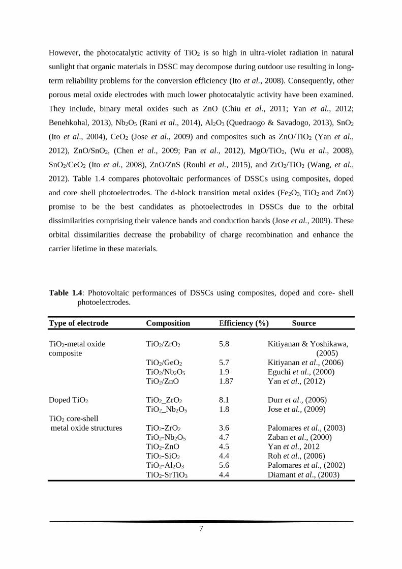
However, the photocatalytic activity of TiO2 is so high in ultra-violet radiation in natural
sunlight that organic materials in DSSC may decompose during outdoor use resulting in long-
term reliability problems for the conversion efficiency (Ito et al., 2008). Consequently, other
porous metal oxide electrodes with much lower photocatalytic activity have been examined.
They include, binary metal oxides such as ZnO (Chiu et al., 2011; Yan et al., 2012;
Benehkohal, 2013), Nb2O5 (Rani et al., 2014), Al2O3 (Quedraogo & Savadogo, 2013), SnO2
(Ito et al., 2004), CeO2 (Jose et al., 2009) and composites such as ZnO/TiO2 (Yan et al.,
2012), ZnO/SnO2, (Chen et al., 2009; Pan et al., 2012), MgO/TiO2, (Wu et al., 2008),
SnO2/CeO2 (Ito et al., 2008), ZnO/ZnS (Rouhi et al., 2015), and ZrO2/TiO2 (Wang, et al.,
2012). Table 1.4 compares photovoltaic performances of DSSCs using composites, doped
and core shell photoelectrodes. The d-block transition metal oxides (Fe2O3, TiO2 and ZnO)
promise to be the best candidates as photoelectrodes in DSSCs due to the orbital
dissimilarities comprising their valence bands and conduction bands (Jose et al., 2009). These
orbital dissimilarities decrease the probability of charge recombination and enhance the
carrier lifetime in these materials.
Table 1.4: Photovoltaic performances of DSSCs using composites, doped and core- shell
photoelectrodes.
Type of electrode Composition Efficiency (%) Source
TiO2-metal oxide TiO2/ZrO2 5.8 Kitiyanan & Yoshikawa,
composite (2005)
TiO2/GeO2 5.7 Kitiyanan et al., (2006)
TiO2/Nb2O5 1.9 Eguchi et al., (2000)
TiO2/ZnO 1.87 Yan et al., (2012)
Doped TiO2 TiO2_ZrO2 8.1 Durr et al., (2006)
TiO2_Nb2O5 1.8 Jose et al., (2009)
TiO2 core-shell
metal oxide structures TiO2-ZrO2 3.6 Palomares et al., (2003)
TiO2-Nb2O5 4.7 Zaban et al., (2000)
TiO2-ZnO 4.5 Yan et al., 2012
TiO2-SiO2 4.4 Roh et al., (2006)
TiO2-Al2O3 5.6 Palomares et al., (2002)
TiO2-SrTiO3 4.4 Diamant et al., (2003)

8
The TiO2 and Nb2O5 structures (composite and doped TiO2) have reported low efficiencies
compared with structures of other combinations (Table 1.4). The efficiencies from doped and
composite structures compare closely for compositions shown. Composite photoanodes of
more than one material have gained interest because they seek to take advantage of best
properties of each component that forms the composite (hybrid). The concept of a composite
goes way beyond a mixture and falls between the concept of a mixture and a compound. The
composite concepts, therefore, fall in a category where the interface between the components
is increased compared to a mixture (Yacaman et al., 1996).
Additionally, the potential of using titanium dioxide and niobium (v) oxide (TiO2/ Nb2O5)
composite has not been fully elucidated. The conduction band of Nb2O5 lying at least 0.25V
above that of TiO2 could make it suitable for the formation of mixed-particles structures
which could result in a higher DSSC photovoltage (Wei et al., 2008). It is of interest to study
TiO2/Nb2O5 composite electrode films fabricated with the goal of exploiting the advantages
of Nb2O5 which include its high stability, high conduction band energy and high transport
rate of injected electrons from dye molecules in DSSC application (Lee et al., 2009). Further,
it will be of interest to explore the electrophoretic deposition technique for film preparation.
1.2 Problem Statement
Film deposition techniques such as screen printing, doctor blade, and sol-gel have been
explored to prepare porous photoelectrode thin films for application in solar cells. The Sol gel
and electrophoretic deposition (EPD) techniques have been used in vehicle painting. Bandy et
al., (2011), fabricated a DSSC based on electrophoretically deposited TiO2 photoelectrodes,
which produced a relatively high ( = 4.91%) conversion efficiency. Notably, the EPD
technique has not been fully exploited in the fabrication of electrodes for application in dye-
sensitized solar cells despite being a relatively inexpensive technique which could be scaled
up for mass production if successfully developed. Additionally, the potential of using
titanium dioxide and niobium (v) oxide (TO2/Nb2O5) composite has not been fully developed.
In this study, we seek to optimize the parameters of electrophoretic deposition technique for
fabrication of nanocrystalline and porous TiO2/Nb2O5 composite electrode thin films and
characterize the films and the assembled dye-sensitized solar cells.

9
1.3 Aim of the Study
The aim of this study is to fabricate and characterize TiO2/Nb2O5 composite thin film
electrodes deposited using the electrophoretic technique for application in dye-sensitized
solar cells.
Specific objectives
The specific objectives of the study are:
1. To optimize electrophoretic deposition (EPD) parameters for fabrication of
TiO2/Nb2O5 composite electrode thin films;
2. To perform structural and morphological characterization of TiO2/Nb2O5 composite
electrode thin films;
3. To carry out optical and electrical characterization of TiO2/Nb2O5 composite electrode
thin films;
4. To fabricate and characterize a TiO2/Nb2O5 based DSSC solar cell through I-V and EIS
characterizations.
1.4 Justification and Significance of the Study
The charge injection and transportation are processes that occur within a photoelectrode and
influence the light to electric energy conversion efficiency in a DSSC. Titanium (IV) oxide
(TiO2) is a key semi-conducting material for fabricating photoelectrodes since they were
successfully employed in 1991 by O’Regan and Gratzel for DSSCs. However, the efficiency
of DSSC is fairly low compared with that of the established silicon based solar cells used in
the market. Composite materials of TiO2 and other metal oxides are being developed to
reduce charge recombination and improve DSSC efficiency. As a technique for fabricating
the photoelectrode thin films, electrophoretic deposition has scarcely been employed in
deposition of composite electrode thin films despite being a cost effective method which can
readily be scaled up for mass production. The outcome of the study will be useful in
producing crystalline, nanoparticulate and nanoporous photoelectrodes suitable for
application in the dye-sensitized solar cells. Such modified photoelectrodes could contribute
to reduction of recombination of charges, improvement in electron injection and transmission
in semiconductors, and enhancement of the conversion efficiency of DSSCs. The uptake of
PV cells in the market could increase if these DSSCs are successfully fabricated with high

10
conversion efficiencies or low production cost or both through use of low cost methods like
EPD. The results of this research will contribute extra knowledge in fabrication of dye-
sensitized solar cells using low cost film-deposition methods.
Thesis outline
The thesis is divided into six chapters. Following this introduction chapter is the literature
review of previous studies on DSSCs and EPD technique. Chapter 2 also discusses the
knowledge gap being filled by this work. The theory governing the calculation of numerical
results is discussed in Chapter 3. In Chapter 4, there is a presentation of the apparatus,
materials and experimental procedures for fabricating TiO2/Nb2O5 composite film. In
addition, the chapter presents procedures for characterizing the fabricated DSSC as well as
the process of obtaining the results. Chapter 5 presents the analysis and discussion of results.
Finally, Chapter 6 summarizes the conclusions drawn from this work and states suggestions
for further work.

11
CHAPTER TWO
LITERATURE REVIEW
2.1 DSSC Structure
A dye-sensitized solar cell (DSSC) comprises a working electrode (dye-sensitized
semiconductor film coated on a TCO) and a counter electrode, sandwiching an electrolyte
containing a red-ox couple as shown in Figure 2.1.
Figure 2.1: Basic structure of a dye-sensitized solar cell (Weerasinghe et al., 2013).
The dye-sensitized photoelectrode (also called photoanode) serves as the working electrode
and consists of porous, nanocrystalline semiconductor film deposited on a glass substrate
coated with a thin film of transparent conducting oxide (TCO). The most common TCO
materials coated on glass substrates include fluorine doped tin oxide (FTO) and indium tin
oxide (ITO) because of their favourable work function as compared to the semiconductor
electrode. The counter electrode consists of glass substrate coated with a TCO layer and
further coated with a catalytic material like platinum. The space between the dye-sensitized
photoelectrode and the counter electrode is imbued with an electrolyte that includes a red-ox
couple. The commonly used red-ox couple is a mixture of iodine and iodide in an organic
solvent. The DSSCs resolve the problem in wide band gap semiconductors insensitive to
visible light by using a dye to inject the electrons across the wide band gap of the

12
semiconductor. The light adsorbed by the dye generates electrons which flow through the cell
resulting in the production of electricity (O’regan & Gratzel, 1991). Research on DSSC is
considered promising due to the dependence of the cell’s light-to-electric-energy conversion
efficiency on its materials. It is noteworthy that the materials alone are not sufficient to
guarantee a highly efficient DSSC, which is also low cost, as its features are intertwined with
the photoelectrode film coating methods (Wang et al., 2012).
2.2 Techniques for Fabricating DSSC Photoelectrode
A major component of a DSSC is the photoelectrode, whose function is to transmit light and
the injected electron to an external circuit. It follows therefore that photoelectrodes should
have the properties of high optical transparency and good electrical conductivity (Gratzel,
2005). To realize an improvement in efficiency of DSSCs, researchers must take into account
the materials used and the film deposition techniques. Techniques employed in fabrication of
photoelectrodes can broadly be categorized into either physical or chemical techniques. The
following is a review, including merits and demerits of the various techniques for
photoelectrode preparation.
(a) Physical deposition techniques
The physical deposition techniques use mechanical or thermodynamic means to prepare and
deposit the materials (Asim et al., 2014). Physical methods can be categorized according to
phase of their precursors whether liquid or gas. The following is a brief review of various
physical deposition techniques used in film preparations.
i) Screen printing
The screen printing technique uses a mesh to transfer a paste onto a substrate by a mechanical
squeegee. During printing, the screen with paste is placed onto the surface on which film is
deposited (substrate) and a squeegee is made to traverse the substrate under pressure. The
screen printing process is detailed in Figure 2.2. This method produces highly reproducible
thick films of around 10-15 microns. It is used in electronic industries to produce massive and
highly reproducible structures. Yan et al., (2012), fabricated DSSCs based on ZnO/TiO2

13
composite thin films using screen printing, colloidal spray coating and electrophoretic
deposition techniques. Their cells produced conversion efficiency of 1.87%.
Figure 2.2: Schematic of diagram of screen printing process (Krebs, 2009).
A high efficiency of 9.1% has been obtained for DSSCs fabricated with porous
nanocrystalline TiO2 films (Yan et al., 2012). However, a major limitation of using the screen
printing method is that it cannot use water as solvent because of formation of cracks on the
film. Water is usually replaced with organic solvents in this technique. Another disadvantage
is the use of organic binders which require thermal activation. Furthermore, constituting the
right paste composition for application in screen printing is usually a tedious process (Tan et
al., 2006).
ii) Doctor blade method
The doctor blade technique, also called tape casting or knife coating is a method in which a
film is deposited by spreading a paste on to a substrate using a slanted blade. The stages of
doctor blade method include paste deposition on glass substrate, paste spreading, and film
drying. A fixed amount of paste is put on a substrate and a glass rod rolled over the paste,
guided by the spacers to determine film thickness (Padinger et al., 2000). Doctor blade
method is a relatively cheap approach for metal oxide paste coatings (Ahmadi et al., 2013).
Some disadvantages of using this technique include wastage of spread out paste, and the
extended time required to determine the best coating parameters (Padinger et al., 2000).

14
iii) Spin coating
Spin coating method uses centrifuge forces to coat a film on a substrate from a suspension
placed onto a substrate and rotated at a high speed. Process of spin coating typically includes
coating, spin up, spin off, and evaporation. The desired film thickness is determined by the
solute concentration in solution, type of solvent, and the continuous rotation of the coated
substrate (Hall et al., 1998). Jin et al., (2012), used spin coating technique to deposit TiO2
films for application in DSSCs and obtained 1.57% efficiency. Chou et al., (2011) also used
spin coating processes to deposit TiO2/NiO composite films on FTO coated glass from a
mixture of TiO2 and NiO powders. The solar cells employing the composite structure yielded
a higher conversion efficiency (3.8%) than that of the screen printed TiO2 film-based dye-
sensitized solar cell (3.27%). The improvement in the conversion efficiency was attributed to
the blocking effect of the NiO particles. The spin coating technique has the advantage of
simple set-up, low power consumption, and produces uniform films. However, the spin-
coating technique has the limitation of requiring a substrate with a flat surface of limited size
(Ahmadi et al., 2013).
iv) Dip coating
The dip coating method consists of immersion and withdrawal processes of the substrate in
material solution at a constant speed. The substrate is dipped in material solution and then
pulled out which occasion the formation of a thin film deposit on the substrate. The coating
thickness is regulated by the speed with which the substrate is pulled: a thicker coating forms
if the removal speed is high. The quality of resulting film depends on surface tension, viscous
force and force of gravity (Scriven, 1988). A novel DSSC based on dip coated porous TiO2
films on an FTO substrate produce a cell efficiency of 10.8% (Ito et al., 2008). This
technique has the disadvantage of using volatile solvents to evaporate solutions on the
coating (Ito et al., 2008).
v) Sputtering
Sputtering involves depositing (metal) on a surface by using fast ions to eject metal particles
from a target. In the sputtering technique, incident particles in the form of ions are
accelerated by an applied electrical potential. Sputtering has been categorized to DC
magnetron sputtering and radio frequency (RF) magnetron sputtering. The RF magnetron

15
sputtering process is suited for insulating materials as it induces a positive charge on the
target surface (Ahmadi et al., 2014). Conflicting results have been reported in the literature
for DSSCs fabricated using RF magnetron sputtered porous TiO2 films on FTO substrate. Jin
et al., (2012), obtained efficiency of 4.60% whereas Jeong et al., (2011), obtained efficiency
too low to be reported. The RF magnetron sputtering has the advantage of allowing direct
sputtering of insulators. A possible limitation of this technique is the obstruction of the RF
radiation by electromagnetic protecting. Additionally, RF networks demand matching
networks and complicated apparatus like power supplies (Awais et al., 2011).
DC magnetron sputtering is an older sputter deposition method than the RF sputter. It is used
for conductive materials and unsuitable for dielectric metal targets. Typical DC magnetron
sputtering equipment operates at an applied potential of between 1,000 and 3,000V, the
vacuum pump of 10-3 Pa, and pressure of about 10 to 16 Pascal. Waita et al., (2009) used DC
magnetron sputtering technique to deposit TiO2 blocking layers for films applied to DSSCs.
An efficiency of 0.78% was obtained for DSSC based on sputter deposited TiO2 thin films on
SnO2:F coated substrates (Hossain et al., 2008). However, Awais et al., (2011), used
magnetron sputtering to fabricate films for application in DSSCs and obtained cell efficiency
too low to be reported. TiO2/Nb2O5 composite films have been fabricated using DC
magnetron technique and consequently, the DSSC based on these composite films yielded
conversion efficiency of 1.86% (Eguchi et al., 2000).
From the reported values of efficiency, sputtering methods appear unsuitable for film
deposition to be used in DSSCS. Some of its advantages include good film adhesion on
substrate, low levels of contamination, good control of deposition temperature and pressure.
The disadvantages of the method include heat generation when plasma electrons bombard the
substrates, low deposition rate, and high pressures of working gas (Hossain et al., 2008).
(b) Chemical deposition techniques
A chemical deposition techniques typically involves a fluid precursor that experiences a
chemical change at a surface of a solid resulting in a solid layer (Choy, 2003).

16
i) Chemical vapor deposition technique (CVD)
The chemical vapor deposition (CVD) method is the result of chemical reactions that occur
between the gaseous reactants close to the surface of a heated substrate. CVD is able to
produce dense materials and still allow manipulations at the atomic or nanometer scale. In
addition, films deposited by CVD are highly uniform, with good adhesion (Choy, 2003). The
method can be used to coat complex-shaped components due to its good throwing power
(Choy, 2003). The CVD rate of deposition is readily adjustable to produce epitaxial thin films
at low deposition rates and thick protective films at high deposition rates. A DSSC based on
nanocrystalline TiO2 thin films deposited by chemical vapor method yielded an efficiency of
0.17% (Shinde, & Bhosale, 2008). However, the cells based on ZnO/TiO2 composite films
deposited by thermal chemical vapor method produced too low an efficiency to be reported
(Kim et al., 2007).
The disadvantages of this technique include, chemical and safety hazards caused by use of
toxic and corrosive precursor gases. These issues however, have been addressed through use
of variants of CVD methods like combustion chemical deposition (CCVD) which employ
more environmentally friendly precursors. Another drawback of CVD is the difficulty in
depositing multicomponent materials due to different vaporization rates of different
precursor. This limitation can be solved by using single-source chemical precursors (Asim et
al., 2014).
ii) Hydrothermal method
Hydrothermal method is suitable for production of semiconductor nanowires at low
temperatures. Hydrothermal method or synthesis involves reactions in aqueous media under
100°C and 1.0 bar pressure conditions (Tacchini et al., 2012). Hydrothermal experiments
require that starting materials be of known composition, highly purified and homogeneous
(Tacchini et al., 2012). Hydrothermal method, followed by a fast dip coating, has been used
by Feng et al., (2012) for preparation of TiO2/ZnO nanowire arrays. Their DSSC achieved an
efficiency of 3.8%. The advantages of hydrothermal method include; ability to induce the
materials to solubility through application of heat and pressure. The products of specific
phase can be readily produced and compounds of specific condensed state can be
synthesized. Hydrothermal method can achieve precise control of the crystallinity of the end
product via adjustment of parameters such as surfactants and precursors, and reaction time.

17
This method also enhances the chemical activities of the reactant. Limitations of
hydrothermal method include the safety issues and difficulties of observing the reaction
process.
iii) Successive ionic layer adsorption and reaction (SILAR)
This is a method that is based on immersion of a substrate into anionic and cationic
precursors, followed by rinsing of the substrate between every immersion in double distilled
water in order to circumvent homogeneous precipitation. The cations are adsorbed onto a
substrate surface via successive immersion of substrate into a cationic precursor. The process
of immersion and rinsing in both cationic and anionic precursors forms a complete cycle. A
multilayer film forms on substrate after a few repetitions of these cycles. Das et al., (2012),
used SILAR and CVD methods to prepare graphene film electrodes for DSSC. Their
fabricated solar cell reached an efficiency of 3.4%. Chung et al., (2012), deposited thin ZnSe
layers on ZnO nanowires using SILAR method for DSSC application. The cells achieved
improved efficiency due to the facilitation of electron transfer. In a SILAR technique, the
deposition of a sufficiently thick film requires an extended period of time which necessities
the use of a microprocessor (Pawar et al., 2011).
iv) Spray pyrolysis deposition (SPD)
In spray pyrolysis method, a solution (precursor) is atomized and its small droplets sprayed
onto a heated substrate which results in the formation of a dry precipitate and thermal
decomposition (Patil, 1999). The technique involves a number of variable parameters that
affect quality of deposited film. These parameters include, deposition temperature, flow rate,
solute concentration in solution, carrier gases, and deposition time. When TiO2 blocking layer
was coated on a substrate by SPD method, the DSSC achieved efficiency too low to be
reported (Jiang et al.,2013). On the other hand, Xia et al., (2007) recorded an efficiency of
3.35% for DSSC fabricated using Nb2O5 blocking layer deposited by spray pyrolysis. Dye-
sensitized solar cells using porous TiO2 films deposited using SPD produced efficiency of
3.2% (Okuya et al., 2002). Unlike SILAR method, spray pyrolysis continuously produces the
films and pyrolysis occurs within the created submicron-sized liquid droplets. Spray pyrolysis
method does not necessarily require high quality substrates.

18
v) Sol-gel coating
The Sol-gel coating is a wet technique which results in a pure, homogeneous, and highly
adhesive film to the substrate. It is a method widely used in the synthesis of materials
originating from a chemical-solution precursor for gel formation. The Sol-gel deposited TiO2
thin films are highly structured and cauliflower-like at the surface, but at the boundary
(interface) with FTO coated glass, they are compact and nonporous (Musembi, 2009). The
Sol-gel method was used by Jin et al., 2010, to prepare nanoporous TiO2 thin films. The
resulting DSSC managed to achieve an efficiency of 1.2%. Efficiency of 0.31% has been
obtained for DSSCs based on mesoporous nanocrystalline TiO2 films deposited using
hydrolysis-limited Sol-gel process (Fu et al., 2009). Notably, the use of Sol-gel technique
results in highly adhesive, homogeneous and pure films and it is a low temperature
processing technique.
vi) Electrophoretic deposition (EPD)
In electrophoretic deposition (EPD), charged particles suspended in a solvent are forced to
move and deposit on an oppositely charged electrode upon application of electric field. The
EPD is fast becoming a promising technique owing to its adaptability, lucidity and cost
effectiveness (Besra & Liu, 2007). Electrophoretic deposition differs from electrochemical
plating in that particles are deposited from suspension whereas in particles are deposited from
solution in the electrochemical plating. In contrast to other physical and chemical techniques
which require high temperatures and pressures, Electrophoretic deposition can be conducted
under normal conditions of pressures and temperatures (Cabanas-polo & Boccaccini, 2015).
The EPD has the limitation of film detachment from the substrate or film crack formation
following the evaporation of residual solvent after film deposition. Films non-chemically
attached to the substrate and adhesion must be effected through firing. An aspect of EPD
explored in this study is the possibility of simultaneously depositing nanoparticles in the
desired ratios leading to fabrication of composite films.
2.3 Factors Affecting Efficiency of DSSCs
A dye-sensitized solar cell is affected by factors related to components such as types of dyes,
electrolytes, counter electrodes and photoelectrodes. These factors are discussed in the
following section.

19
(a) Types of dyes
The dyes (photosensitizers) absorb sunlight photons and inject electrons to the conduction
band (CB) of the wide band gap metal oxide constituting the photoelectrode (O’Regan &
Gratzel, 1991). For photosensitization of TiO2-based DSSCs, Ruthenium polypyridyl dyes
have proved to be most efficient due to their broad absorption spectra combined with
favorable photo-electrochemical properties and high stability in the oxidized state (Bingwen
et al, 1997). The most commonly used ruthenium complex dyes in DSSCs include N719 or
Ruthenium 535-bisTBA dye whose chemical formula is (RuL2(NCS)2TBA)2, where L=2,2’-
bipyridine-4,4’-dicarboxylate and N3 (black dye, RuL4(NCS)2), (Boschloo & Hagfeldt,
2009).
The conversion efficiency of ruthenium dyes based DSSCs is still better than that of cells
sensitized with other types of dye compounds like chlorophyll derivatives (Kay & Gratzel,
1993). Ruthenium (Ru) metal dyes have the disadvantage of low molar absorption coefficient
in short wavelength regions (about 350 nm - 500 nm). Therefore, efforts have been devoted
to synthesize dyes with high molar absorption coefficient in order to improve DSSC
efficiency (Boschloo & Hagfeldt, 2009; Qin & Peng, 2011).
(c) Types of electrolyte
The electrolyte in dye-sensitized solar cell (DSSC) transfers electrons from the counter
electrode to the oxidized dye thus completing the circuit. Electrolytes for DSSCs are
categorized into liquid, solid, and quasi-solid state electrolytes based on their viscosities (ψ).
A liquid state electrolyte typically comprises organic solvent, red-ox couple, and additives
with the red-ox couple being the major component. The iodide/triiodide (
3/ II ) red-ox
couple is obtained when lithium iodide or other iodide compounds like potassium iodide and
iodine are dissolved in organic nitrite solvents. The iodide/triiodide red-ox couple has
advantages of good solubility in organic solvents, rapid dye regeneration, suitable red-ox
potential, and high conversion efficiency (Boschloo & Hagfeldt, 2009). However, the
3/ II
red-ox couple has the limitations of low open circuit voltage (VOC) and corrosion of
electrodes. Other types of red-ox couples including (
3/ BrBr (Ferrere et al., 1997),
3)/(SCNSCN (Oskam et al., 2001), and
3)/(SeCNSeCN (Wang et al., 2004) have been

20
synthesized and investigated for use in DSSCs. The efficiency of DSSCs with iodide/triiodide
electrolyte red-ox couple, however, remains unmatched by that of cells based on alternative
red-ox couples.
Another component of liquid electrolyte is the organic solvent. It functions to facilitate the
dissolution and diffusion of iodine/triiodide ions. Acetonitrile (ACN) and 3-
methoxypropionitrile (MePN) have been widely used for DSSC electrolytes because they are
low viscosity and low boiling point solvents. Decreasing viscosity of the solvent increases the
short circuit current due to better diffusion of the red-ox couple. Acetonitrile is preferred to
MePN because of its excellent stability, and capability to dissolve salts (Pugliese, 2014).
However, a demerit of using acetonitrile and iodine in liquid electrolytes includes the
potential environmentally adverse effects contributed by these chemicals.
Electric additives constitute the other component of liquid electrolyte. They are employed to
suppress charge recombination in DSSCs. The most efficient additives are 4-tert-
butylpyridine (4TBP) (Kopidakis et al., 2006), methylbenzimidazole (MBI) (Figgemeier &
Hagfeldt, 2004), and Lithium (Li) cations (Mehmood, 2014). The most probable mechanism
is that these additives adsorb on the semiconductor surface and block the reduction sites to
keep tri-iodide ions away from contact. The main disadvantages of liquid electrolytes include
solvent leakage and corrosion of terminals affecting the long-term stability of the cells.
SurlynR ionomer resin is a sealing material used to reduce liquid electrolyte leakage as well
as resist corrosion from iodine. (Snaith & Schmidt-Mende, 2007).
(d) Types of counter electrodes
The counter electrode (CE) comprises a catalyst deposited on a transparent conductive oxide
(TCO) to facilitate reduction of excited dye. The preferred catalyst is platinum (Pt) because
of its high exchange current density, high catalysis, and transparency (Boschloo & Hagfeldt,
2009). The performance of CE depends on the method of Pt deposition on the TCO coated
glass substrate. The deposition methods include thermal decomposition of hexachloroplatinic
salt in 2-propanol (Hafez et al., 2012), sputtering (Nazeeruddin et al., 1993), and spin coating
(Lee et al., 2001). The deposition method affects the charge-transfer resistances and stability
of the counter electrode. It is reported that the activity of the platinum (Pt) catalyst decreases
with time in presence of iodide/triiodide red-ox couple due to alteration of its electrocatalytic
properties (Mehmood, 2014). Despite showing excellent catalytic action, platinum has the

21
disadvantage of being an expensive material. Deposition processes require annealing of the
film at relatively high temperatures (450 °C) to form a film on FTO. This high temperature
treatment of the film limits the application of this method to plastics and other thermally
sensitive materials. Graphene, carbon and conductive polymers have been synthesized as
alternative catalytic materials to replace platinum based on their high electronic conductivity,
and good reactivity for triiodide reduction (Li et al., 2012). However, the DSSCs based on
these alternate catalytic materials have been low due to lower catalytic activity for triiodide
reduction compared with Platinum.
(d) Photoelectrodes for dye-sensitized solar cells
In 1991, O’Regan and Gratzel developed the first dye-sensitized solar cell based on highly
effective porous titanium dioxide (TiO2) electrodes. TiO2 is a material that is non-toxic,
transparent, abundant-, environmentally stable, chemically resistant and relatively cheap
(Gratzel, 2005). TiO2 has extensively been used, in conjunction with ruthenium dye complex,
as a photoelectrode for the fabrication of DSSCs because of its overall high conversion
efficiency. Titanium dioxide is a semi-conducting oxide that has three crystalline
polymorphs, namely anatase (Eg = 3.23 eV), rutile (Eg = 3.05 eV), and brookite (Eg = 3.26
eV) (Nowotny et al., 2008). The Fermi level of rutile is 0.1 eV lower than that of the anatase,
making anatase preferable in DSSCs applications. However, the application of TiO2 in
DSSCs is hindered by recombination of the photo-generated electrons with the red-ox couple
in electrolyte limiting the conversion efficiency.
Other metal oxides have been examined as photoelectrodes for DSSCs application and their
films fabricated by variety of deposition techniques. They include ZnO (Chiu et al., 2011),
Nb2O5, (Rani et al., 2014), Al2O3 (Quedraogo & Savadogo, 2013), and CeO2 (Jose et al.,
2009). Although the DSSCs based on individual performances of these semiconductors are
not so efficient, some of their combinations have shown promising results. Consequently,
composites such as MgO/TiO2, (Wu et al., 2008), SnO2/CeO2 (Ito et al., 2008), ZnO/SnO2
(Chen et al., 2009; Pan et al., 2012), ZnO/TiO2 (Yan et al., 2012), ZnO/ZnS (Rouhi et al.,
2015), and ZrO2/TiO2 (Wang et al., 2012), have been explored for application as
photoelectrodes. However, the conversion efficiencies of solar cells fabricated from these
materials are much less (η < 6%) than those of TiO2 based solar cells which presently stand at
η = 11.8% (Yella et al., 2011). Solar cells from composites of TiO2/other metal oxides

22
showed relatively higher efficiencies. Niobium (V) oxide and titanium (iv) oxide
(Nb2O5/TiO2) composite electrode films will be investigated in this study. Niobium (V) oxide
(Nb2O5) is a semiconductor with a wide band gap energy(Eg) of 3.49 eV (Jose et al., 2009),
which is larger than Eg of TiO2 by 0.29 eV (Sancho-Parramon et al., 2008). Nb2O5 based
photoelectrodes in DSSCs, sensitized with N3 dye produced higher VOC than TiO2 based
photoelectrodes in DSSCs. The higher VOC for Nb2O5 based cells was attributed to its higher
conduction band edge compared with TiO2 and larger optical band gap (Hara et al., 2000). In
this study, photoelectrodes formed through a mixed particle structure are expected to
incorporate an alteration in CB edge in composites of TiO2 and Nb2O5 thus yielding high VOC
for DSSCs.
2.4 Electrophoretic Deposition (EPD) and Factors Affecting Film Deposition
As mentioned earlier, electrophoretic deposition (EPD) is a colloidal method in which an
applied DC electric field force charged particles suspended in a solvent to move and deposit
on an oppositely charged electrode resulting in formation of a condensed film as shown in the
following Figure 2.3.
Figure 2.3: Schematic drawing of the EPD setup showing cathodic deposition of charged
particles of mixed metal oxides.(Dickerson & Boccaccini, 2012).
Cathode Anode
DC supply
V
A

23
The EPD technique has been studied since 1807 when Ruess first observed that solid particles
(clay) suspended in water moved upon application of an electric field (Sarkar & Nicholson,
1996). Hamaker was the first scientist to study and apply EPD to ceramics (Hamaker, 1940).
The kinetics of EPD is not yet well understood and scientists continue to investigate the
process as they seek to develop a quantitative understanding of its kinetics and thus enable its
application in material processing (Dickerson & Boccaccini, 2012). The EPD technique has
the advantage of simple equipment, rapid coating production, high reproducibility,
adaptability to mass production processing, and low cost of film fabrication (Boccaccini, et
al., 2010). Compared to other film forming techniques like screen printing and doctor blade,
EPD process offers ease in controlling the morphology and thickness of a deposited film by
simple alteration of the particle concentration in suspension, deposition time, and applied
electric voltage. Unlike electrochemical plating in which deposition is from a solution,
electrophoretic deposition uses charged particles (metal oxides) in suspension.
The characteristics of electrophoretically deposited films may be controlled by EPD
conditions and parameters, including the nature and choice of solvent, charging mechanism,
particle concentration in suspension, electric field strength, and deposition times (Dickerson
& Boccaccini, 2012). Various authors have applied different combinations of these EPD
conditions to deposit TiO2 -based nanostructured films (Table 2.1). Following is a brief
review of the EPD processing conditions/parameters.
(a) Particle charging mechanism
The electrophoretic deposition process is governed by the particles ability to develop electric
charges when suspended in a liquid. Iodine, Zinc nitrate Zn(NO3)2 and Magnesium nitrate
hexahydrate (Mg(NO3)2.6H2O, and have been used as additives in previous studies to
constitute charging mechanisms of single or many nanoparticles systems as shown in Table
2.1. Particle charging of nanoparticles using Mg(NO3)2.6H2O is achieved by adsorption of
MgNO3+ to the particle surface (Yum et al., 2005). It is believed that in the case of iodine
additive, the particle charging mechanism is achieved through adsorption of protons
(Benehkohal, 2013).

24
Table 2.1: Summary of electrophoretically deposited TiO2 based films applied to dye-
sensitized solar cells.
Nano-structure
Substrate Solvent Additive EPD parameters
Efficiency (%)
Reference
TiO2 layers ITO-PET _ _ d=0.3 mm,
DCV=6 V, t=0.5-1 min.
4.30
Miyasaka & Kijitori (2004)
TiO2 nP ITO-PET 2-propanol Mg(NO3)2
.6H2O d=2 cm, c=2.5 g/L, DCV=20-160 V, t=180 s.
1.03
Yum et al., (2005)
TiO2 nT FTO Methanol & water
__ __ 6.72 Kim et al., 2007
TiO2 nP FTO d=1 cm, c=10 g/L, DCV=5-20 V t=1-8 min
__
Jarernboon et al., (2009)
TiO2 nP FTO 2-propanol Mg(NO3)2
.6H2O d=2 cm, c=2.5 g/L, DCV= 20-60 V, t=15 min.
4.91
Bandy et al., (2011)
TiO2/ZnO ITO-PEN 2-propanol _ d=1.5 cm, c=2.5 g/L, I=20 μA/cm2, t=5 min.
5.54
Chiu et al., (2011)
TiO2 Flexible-glass
Mg(NO3)2
.6H2O d=2 cm c=0.25 g/L DCV=75 V t=3 min
__
Lee et al., (2011)
ZnO/TiO2
comp FTO Ethanol &
water _ d=1.5 cm,
c=1.33 g/L, DCV=60 V.
0.10
Yan et al., (2012)
TiO2 nP FTO & PEN-ITO
Ethanol/2-propanol/ Butanol
I2 d=7 mm, c=33.3 g/L, DCV=30 V
5.20 Xue et al., (2012)
TiO2/ZnO comp
FTO& stainless steel
Water & 2-propanol
Zn(NO3)2
d=2 cm, c=5 g/L, DCV=3.1 V, t=5-15 min.
5.57
Benehkohal, (2013)
KEY: nP nanoparticles, nT nanotube, nR nanorods, comp composites, d electrodes
separation, c particle concentration, DCV applied (DC) voltage, I current, and t deposition
time.

25
(b) Particle concentration in suspension
The particle concentration in electrophoretic deposition (EPD) suspensions constitutes
another important parameter in electrophoretic deposition process with values as low as 0.25
g/L up to 33.3 g/L reported in the literature (Table 2.1). According to Hamaker’s Equation
(2.1), the deposit mass (thickness) increases exponentially with particle concentration in
suspension. This finding has been confirmed in practice as reported by Ata et al., (2014)
among other authors (Figure 2.4). It can be seen from the Figure 2.4, that deposition rate was
high for concentrations lower than 0.1 g/L and no significant variation in deposit mass was
observed at higher concentrations. Radice et al., (2010), however, noticed that no deposit was
formed in some systems below a particular particle concentration independent of applied
voltage or deposition time. Indeed, Ata et al., (2014), could not obtain film deposition below
a concentration of 0.05 g/L. Since a wide range of values for particle concentrations has been
reported, it was difficult to determine the optimum value of particle concentration in
suspension to enable deposition of composite films suitable for intended applications by EPD
the method.
0.00 0.08 0.16 0.24 0.32 0.40 0.480.0
0.7
1.4
2.1
2.8
3.5
4.2
Mas
s (m
g cm
-2)
Particle concentration (g/L)
Figure 2.4: Typical deposit mass versus particle concentration for films prepared from 10
g/L TiO2 suspension in ethanol for deposition time of 5 min and applied voltage of
40V, and (Ata et al., 2014).

26
(c) Electric field strength
Typical configuration of electrophoretic deposition technique involves parallel arrangement
of electrodes. The electrode separation distance )(l is usually fixed to provide constant and
uniform electric field strength l
V for film deposition. As an EPD process parameter,
electric field strength leads to a linear increase in deposition mass according to Hamaker’s
equation (Besra & Liu, 2007);
tb
V
ψξcm r
1
3
20 (2.1)
where m is the deposited mass, c is powder/particle concentration in the suspension, 0ς is
permittivity of free space, r is relative permittivity of the solvent, ξ is the zeta potential of
the particles, is the viscosity of the solvent, V is the applied DC voltage, b is the
distance between the electrodes, and t is the deposition time. Electric fields in range 10 V/m
to 50 V/m have been applied in EPD technique as shown in Table 2.1.
Low fields (around 20 V/m) result in good film assembly Basu et al., (2001). However,
Konig et al., (2008) observed that suspensions in organic liquids generally require high fields
( > 100 V/m) due to their low dielectric constants. In many EPD applications, applied voltage
(V) values for fixed electrode separation distances are frequently used rather than electric
fields values (V/m). The setback of using high voltages, however, is the film quality
deterioration. Moderate applied DC voltages (25 – 60 V) may provide uniform films for
DSSC application.
Electrophoretic deposition techniques can be conducted either under constant voltage or
constant current while, in either case, keeping the particle concentration in suspension either
constant or changing with deposition time. Although constant-current depositions can provide
better and easier control over the EPD process for thick films, constant-voltage conditions are
ideal for thin films and allow for uniform microstructures (Nyongesa et al., 2007). The
challenge is in optimization of the applied electric potential to fabricate films suitable for the
intended applications.

27
(d) Nature of the solvent
The first EPD process used water as the solvent (Hamaker, 1940). The use of water as a
solvent has many advantages including, its environmentally friendly nature, low cost, wide
availability, ability to control higher temperature during the deposition, and faster EPD
kinetics due to high dielectric constant (Dickerson & Boccaccini, 2012). However, high
electric fields cause electrolysis of water, adversely affecting the quality of the deposits
formed (Besra & Liu, 2007). Other liquid solvents like 2-propanol (Yum et al., 2005; Bandy
et al., 2011; Chiu et al., 2011), and mixtures of water and organic liquids like methanol &
water (Kim et al, 2007), ethanol & water (Yan et al., 2012), and water & 2-propanol
(Benehkohal, 2013) have been explored as alternatives to use of water in EPD (Table 2.1).
Organic solvents are only little affected by relatively large values of electric field as their use
results in little or no electrolysis (Besra & Liu, 2007). The choice of liquid solvent used in
EPD is influenced by values of viscosity and relative dielectric constants of solvents suitable
for type of film application (Table 2.2.).
Table 2.2: Physical properties of solvents (Dean, 1999).
Methanol 0.557 32.63
Ethanol 1.089 24.55
1-Propanol 1.937 20.13
2-propanol 2.857 18.30
2-butanol 2.588 17.26
Acetonitrile 1.090 37.50
Water 0.890 80.10
Besra & Liu, (2007), used these organic solvents to determine the incidence of deposition for
beta-alumina suspensions as function of dielectric constant (ε) of liquid. They obtained film
deposition for liquids with dielectric constants in the range of 12-25. Deposition failed for
EPD of films from solvents of too low (< 12) dielectric constant (ε) because of insufficient
dissociative power. Deposition also failed for electrophoretically deposited films from
solvents with too high (> 25) dielectric constant due to the high ionic concentration in the
Solvent Viscosity [ψ] cP(=10-3Ns/m2)
at 20°C
Dielectric constant
)( at 20°C

28
solvent which contributed to reduction of electrophoretic mobility of charged particles
(Miyasaka & Kijitori, 2004). According to the Derjaguin-Landau-Verwey-Overbeek (DLVO)
theory, it is noted that that for particle concentrations above a crucial value, the repulsive
forces were overcome by the attractive Van der Waals forces resulting in coagulation.
(Dickerson & Boccaccini, 2012). The best solvents for EPD suspension are characterized by
low viscosity values and high deposition rate (Benehkohal, 2013). 2-propanol, despite having
relatively higher viscosity than other solvents, has low relative dielectric constant (18.30) and
becomes a favorable candidate solvent for electrophoretic deposition of composite films.
(e) Deposition time
The film deposition rate for a constant applied electric field and constant particle
concentration in the EPD process is known to decrease with increased deposition time (Besra
& Liu, 2007). A typical variation of deposit mass (approximated by film thickness) with
deposition time is shown in Figure 2.5 (Nuryadi & Aprilia, 2012). Initially, the thickness
increases nearly linearly and attains a plateau at higher deposition times. For EPD at constant
voltage and fixed distance, the plateau results from decrease in EPD electric field possibly
due to creation of a non-conducting film deposited on the surface of the electrode. The results
are consistent with theoretical predictions based on Hamaker’s equation (2.1). Jarernboon et
al. (2009) approximated the optimum TiO2 film thickness to z ~ 14μm for the highest DSSC
efficiency. Films of such thickness are highly porous and therefore very favorable for
application in DSSCs where there is increased dye loading. Films of thickness larger than
14μm result in deterioration of film adhesion to the substrate. Our literature review however
established that the efficiency obtained by Jarernboon et al., (2009), was too low to be
reported.
An optimized-photoelectrode film thickness (z) is required to address the conflict between
light harvesting and charge transport and thus enhance conversion efficiency. Electrophoretic
deposition (EPD) technique is explored as alternative technique to deposition techniques to
overcome the challenge of film thickness control, a factor affecting efficiency of resulting
solar cell (Vilarinho et al., 2013).
From the literature, we have seen that various techniques can be used to fabricate DSSCs.
Although screen printing method is good, it is limited in its inability to use water as solvent
because of crack formation in deposited films upon firing. Other limitations of spin coating

29
process include the low efficiencies and requirements for a substrate with a flat surface of
limited size.
0.0 0.5 1.0 1.5 2.0 2.5 3.0 3.50
5
10
15
20
25
30
35
Thic
kness
(m
)
Deposition time (s)
Figure 2.5: Typical TiO2 thickness versus deposition time of BNT electrophoresis for
acetone with iodine –based suspension (Vilarinho et al., 2013)
Although dip coated films used in DSSC produce high efficiency (10.8%), the technique has
disadvantage of using volatile solvents to evaporate solutions on the coating surfaces (Ito et
al., 2008). Electrophoretic deposition technique has been widely explored due to its
advantage including, simple equipment, high reproducibility, rapid coating production, and
low cost of film fabrication. It also offers an easy manipulation of the morphology and
thickness of a deposited film via simple control of the process parameters. Moreover,
electrophoretic deposition can be achieved at standard temperature and pressure. Although it
produces films of low efficiency, in this work, we wish to explore the use of EPD for the
fabrication mixed-particle composites of TiO2 and Nb2O5 for application in dye-sensitized
solar cells.

30
2.5 Electrochemical Impedance Spectroscopy Characterization of DSSC
Electrochemical impedance spectroscopy (EIS) is an important tool for examining the
qualities and properties of dye-sensitized solar cells. It enables separation of interfacial
capacitances, electron-transfer resistances, charge and ions diffusion components in the film
and electrolyte respectively. Before the advent of DSSC, EIS was largely put to use in
photoelectrochemistry (Bisquert, 2002). Photoelectrochemistry is a field investigated using
electrodes comprising monocrystalline semiconductors for light to electric energy conversion
(Bisquert, 2002). In these systems, EIS supply information on the rates of charge transfer at
the interface as well as on the concentration of electrons at the surface (Bisquert & Fabregat-
Santiago, 2010). Impedance replaces resistance as a more general circuit parameter. In dye-
sensitized solar cells, the transport of electrons through TiO2 film by diffusion is coupled
with recombination at the TiO2/electrolyte boundary. The impedance of electronic diffusion
and recombination at the photoelectrode/electrolyte interface in a DSSCs has been widely
studied (Bisquert, 2002; Adachi et al., 2006; Fabregat-Santiago et al., 2007).
A key concept in the DSSC analysis is the chemical capacitance which is normally absent in
classical photo-electrochemistry but is critical in the analysis of techniques requiring
frequency-resolution in dye-sensitized solar cells (Bisquert & Fabregat-Santiago, 2010).
Analysis of EIS measurements often involve use of Nyquist plot whose limitations include
the inexplicit frequency presentation on the plot and small impedances being swamped by
large impedances. Operation of conventional solar cells has been well explained using
equivalent circuits. Han et al., (2004), investigated internal resistances of DSSC using EIS
measurements and observed that resistance elements associated with charge transport at the
dye/TiO2/electrolyte interface displayed diode-like behaviour.
A typical electrochemical impedance spectrum for a high performing DSSC displays three
arcs in the Nyquist plot: two small ones on both sides of a large central arc (Figure 2.6). The
arc on the left, for impedances measured at high frequencies, relates to the charge transfer
process at the Platinum coated counter electrode (RCE) while the arc on the right (for
impedances at low frequencies) can be attributed to Warburg resistances (Zd) in Nernst
diffusion process of
3I ions in the electrolyte. The central arc (in intermediate-frequency
region) corresponds to charge transport resistance in TiO2 film (Rt), charge transfer
(recombination) at the TiO2/dye/electrolyte interfaces (Rct) and the chemical capacitance (Cμ).

31
Figure (2.6b), shows the characteristic frequencies inserted in the graph in the order of
increasing frequency whereby, d corresponding to diffusion of red-ox ions in electrolyte,
r to electron recombination with red-ox species, t to electron diffusion in TiO2, and CE
to charge transfer at pt/electrolyte interface (Sarker et al., 2014).
Figure 2.6: Typical experimental impedance spectra for DSSC with an ionic liquid based
electrolyte (a) at open circuit conditions 0.6 V, (b) the Gerischer impedance spectra
whereby recombination resistance is less than transport resistance (Fabregat-Santiago et
al., 2011; Sarker et al., 2014).
The EIS spectra of DSSCs do not always show three distinct arcs in the Nyquist plot as
evidenced by Nyquist plots exhibiting only the central arc correspond to Gerischer impedance
(Figure 2.6c). In such a case, the experimental data must be properly inspected to assist
efficient extraction of the physical parameters of the cell. Physical parameters of a solar cell
can be derived from cell EIS spectra by fitting the spectra to an equivalent electric model.
Several researchers (Bisquert et al., 2000; Fabregat-Santiago et al., 2005; Wang et al., 2005)
have developed equivalent circuits’ models to characterize DSSCs. The most widely used
equivalent circuit model on DSSCs is the transmission line model due to its accuracy in
modeling the cells physical properties (Sarker et al., 2014).

32
CHAPTER THREE
THEORETICAL FRAMEWORK
This chapter gives theories relating to the working of a DSSC, EPD deposition technique, EIS
and characterization of films and cells.
3.1 The Working Principle of a Dye-Sensitized Solar Cell (DSSC)
The working principle of a dye-sensitized solar cell (DSSC) is depicted schematically in
Figure 3.1. A dye-sensitized solar cell is a photo-electrochemical system, in which a porous,
nanocrystalline semiconducting metal-oxide film sensitized with dye molecules and
deposited on a transparent conductive glass substrate (such as FTO), serves as a
photoelectrode or working electrode (Zhang & Cao, 2011). A counter electrode comprises a
catalyst (usually platinum) coated on conducting glass plate.
Figure 3.1: Schematic diagram of the working principle of a dye sensitized solar cell.
Each component in the DSSC is represented by an isolated block while each electron
transfer process is represented by a letter. The vertical line on the right indicates the
energy scale in eV and the energies of each functional material are represented by
horizontal lines (Luo et al., 2009).
Conductive band
(metal oxide)
HOMO (Dye)
Redox potential
(electrolyte)
Valence band
(metal oxide)
Dye
(D* D+)
D
F
G
B
Gla
ss
s
ub
stra
te
pla
tesu
bst
rate
Co
nd
uct
ing
gla
ss
pla
te
EV
A
(hv)
Cat
aly
st (
Pla
tin
um
film
)
E (eV)
LUMO (Dye)
Electrolyte
VOC
EC
H
Load
Photoelectrode Counter electrode
I
3I
FT
O
e
(D D*)
C
E

33
The space between the two electrodes is usually filled with a liquid (or solid) electrolyte
containing red-ox couples such as
3I/I , and serves as an electric conductor between the two
electrodes. In Figure 3.2, the different electron transfer processes are represented by letters A
to G. The light adsorbed by the dye produces electrons which flow through the cell resulting
in the generation of electricity (O’regan & Gratzel, 1991).
According to Gratzel (2005), the change of solar energy into electric energy using a solar cell
is the result of the dynamic competition between the forward processes (A-E) and back
processes (F-H) as indicated in Figure 3.2.
Process A: Photon absorption and dye excitation. The dye molecules adsorbed on the
semiconductor film absorb light photons incident on the solar cell. A photon of energy hν is
absorbed by the dye in the ground state ( D ) and which promotes it to an excited state (*D )
according to equation (3.1).
*DhD (3.1)
Figure 3.2: The charge transfer kinetics and associated timescales (rates) in DSSC The
letters A, B, C, D,& E represent forward and desired processes while letters F, G & H
represent recombination processes (back reactions) in the cell. (Rahman et al., 2015).

34
Process B: Electron injection. The excited dye ( *D ) injects electrons ( e ) into the
conduction band (CB) of the semiconductor film and becomes oxidized ( D ). The time rate
of occurrence of this process is on 1010 - 1012 s-1 scale.
eDD* (3.2)
Process C: Electron transport. The injected electrons are transported by diffusion along the
semiconductor particulate network towards the external conducting FTO coated glass, via the
external load to the platinum-coated FTO counter electrode. Transport of injected electrons
occurs by diffusion rather than drift due to negligible field across the semiconductor film.
Electron diffusion in film takes place in order of 100-102 s-1 time scale (Figure 3.2).
Process D: Reduction of the red-ox couple at platinum electrode. Finally, the injected
electrons reduce triiodide (
3I ) ions to iodide ( I3 ) ions according to
IpteI 3)(23 (3.3)
This process is in order of 103 S-1 scale (Rahman et al., 2015).
Process E: Regeneration reaction of dye in red-ox couple. After electron injection into
semiconductor by the dye, a positively charged (oxidized) dye remains. This oxidized dye
( D ) is reduced to ground state by a red-ox couple in the electrolyte. The highest
regeneration efficiency has been achieved by iodide/triiodide (
3/ II ) red-ox species. The
equation for reduction of oxidized dye is given by equation 3.4;
eDID 23 (3.4)
This regeneration process is in the order of 108 s-1.
The processes A to E are forward and desirable processes. However, there exist some back
reactions (recombination) denoted by processes F to H as outlined in following section which
are not desirable.

35
Electron Recombination Processes.
Process F: Decay of the excited dye to the ground state,
DD * (3.5)
As shown in Figure 3.2, recombination by dye decaying to the ground state is limited because
it takes place in the nano second range which is slower than the electron injection happening
in the picoseconds range.
Process G: Recombination of oxidized dye with the injected electrons,
DeD * (3.6)
The process takes place in order of 106s-1. This process contributes to reduction of electron
density in the TiO2 leading to a change in the energy of the TiO2 conduction band, thus
directly affecting the VOC (Maluta, 2010).
Process H: Capture of injected electrons by the tri-iodide in the electrolyte. As electrons
diffuse through the TiO2 (metal oxide) film, some electrons may become trapped at the
surface of the TiO2 particles and recombine with
3I ions in electrolyte. This back reaction
(recombination process) is represented by equation (3.7) which resembles equation 3.3 for
reduction of red-ox couple at counter electrode;
IIe 32 3 (3.7)
Some of portions of FTO coated glass surface will inevitably get uncovered by the film thus
necessitating the electrolyte to reach it thereby causing electron leakage. The recombination
takes place at 101 to 100 s-1.
Electron transport
The electron transport mechanism in a DSSC is related to the matching of energy levels
between the CB of the semiconductor and the excited state of the dye. The semiconductor
nanoparticle network serves as a transporter of the electrons injected by the dye molecules.

36
Electrons do not drift through the film but instead diffuse through it. The drift of electrons
through the film is out ruled because of the small size of the nanoparticles forming the film
which inhibits the creation of a built-in electric field and a space charge layer inside the
particles (Pugliese, 2014). There exists sub-band gap states in the semiconductor film that
influence the electron transport. Electrons diffuse through the film characterized by a de-
trapping of electrons from these sub-band gap states (Hagfeldt & Gratzel, 2000). The electron
diffusion is caused by non-uniformity or gradient in electron concentration generated by the
collection of the electrons in the conduction band of the semiconductor particles under light
irradiation.
The traps characterizing the electron diffusion are localized energy states within band gap
and just below the conduction band margin of the metal oxide. The quasi-Fermi level rises in
a cell exposed to a high illumination and the number of traps increases resulting in a high
photocurrent. If the cell is exposed to low illumination, a low photocurrent is obtained since
contribution to electron transport is only by the deep traps. (Hagfeldt & Gratzel, 2000). Three
important parameters in the electron transport process include electron diffusion length ( dL ),
electron lifetime ( n ) and diffusion coefficient ( nD ). Electron diffusion length ( dL ) is
defined by the average distance the electron travels through the semiconductor before
recombination. Electron lifetime ( n ) is the period from electron generation until
recombination or extraction. The diffusion process can be expressed in terms of diffusion
coefficient ( nD ). The electron diffusion length ( dL ) is determined by taking the square root
of the product of the effective diffusion coefficient (Dn) and lifetime ( n ) as given in the
following equation (Wang et al., 2004);
nnd DL (3.8)
The electron diffusion length in DSSCs can be measured by incident photon conversion
efficiency (IPCE) or electrochemical impedance spectroscopy (EIS) methods (Jennings et al.,
2010; Maluta, 2010). In case electron diffusion length ( dL ) is equal to or greater than the film
thickness ( zLd ), all the photogenerated electrons will be statistically collected, raising the
current density and efficiency of the cell (Pugliese, 2014). In terms of time, a good solar-cell
performance must meet the condition that the electron extraction or transport time should be

37
shorter than the electron lifetime ( nt ) to enable the electrons to reach the front
electrode before recombination. Intensive research efforts have been focused on how to
enhance forward processes (A-D) and suppress the back reaction or charge recombination in
process (D-G) and thereby increasing the conversion efficiency( η ).
3.2 Solar Radiation and Materials for Solar Cells
The efficiency of a solar cell is controlled by the variations of the intensity of spectral
irradiance of the incident light. The solar radiation impinging the Earth surface depends on
factors such as location, atmospheric conditions, and time of the day. Consequently, a power
density and standard spectrum have been defined to provide for an accurate cell I-V
characterizations as well as comparison among different solar cells. Figure 3.3 shows two
curves for comparison: a zigzag one for the sun’s radiations received on the earth and a
continuous curve for black body at a temperature of around 6000 K. The solar spectrum is
similar in shape to that of black body and is influenced by adsorption of some molecules such
as ozone gas and water in the atmosphere (Figure 3.3). The optical path through which the
solar radiation passes through before reaching the ground depends on the Sun’s position and
is called Air Mass (AM). The standard air mass used for solar cell testing is AM 1.5G where
G stands for Global which is the sum of direct and diffuse light (Weeranghe et al., 2013).
The solar cell efficiency also depends on the structure and morphology of photoelectrodes of
the DSSC because these properties affect the optical and electronic properties of the
photoanode. Porous nanostructures making the photoelectrodes present a larger surface area
for adsorption of the dye leading to an enhanced light absorption from a substantial part of
the solar spectrum. Materials with wide optical band gaps display a poor reaction to light in
the visible region (0.4 < λ < 0.7 μm, Figure 3.3). This challenge is overcome by coating them
with dyes to extend their optical absorption into the visible light region. Titanium dioxide
(TiO2) (Eg = 3.23 eV) (Jose et al, 2009) and Niobium (v) oxide (Nb2O5) (Eg = 3.49 eV)
(Sancho-Parramon, et al., 2008) are wide-band gap materials and only about 8% of light
photons (E = 1.77 - 3.2 eV) are capable of promoting electrons from the valence band to the
conduction band of TiO2 or Nb2O5. The wide-band gap materials are chemisorbed with dye
molecules to enable them to function as solar cell materials. A key requirement of solar cell

38
materials is the ability to allow radiation in the visible light region (shown by parallel dashed
lines in Figure 3.3) to go through them and excite the dye.
Figure 3.3: Spectral irradiance against wavelength requirement for solar cell materials.
The two vertical dashed lines represent the visible region of the electromagnetic spectrum
(Smestad et al., 2008).
Methods for fabricating photoanodes for DSSC are determined by their ability to deposit
highly porous films that provide increased surface area for dye attachment and electrolyte
penetration. The electrophoretic deposition technique (EPD) is explored in this study to
fabricate photoanodes comprising of TiO2/Nb2O5 composite films for application in dye-
sensitized solar cells.
3.3 Possible Film Structures from EPD Deposition
There are three possible film structures obtained when two particles are deposited
simultaneously using EPD technique: Core-shell film structures (Diamant, et al., 2004;
2011), mixed particles-composite structures (Chou et al., 2011) and layered film structures
(Paula et al., 2014). Core-shell structures comprise a core structural domain of nanostructures

39
such as nanoparticles, or nanowires, and a shell structural domain of a coating layer covering
the surface of core nanomaterials (Figure 3.4a). Since TiO2 is the material of choice in
fabricating photoelectrodes for DSSC, it is typically used as the core material while other
metal oxides like MgO, ZnO, ZrO2 are used as the overlayer materials in core-shell
structures.
Figure 3.4: Possible film structures of two-particle EPD deposition (a) Core-shell
structures (b) mixed particles structure and (c) layered structures. (Diamant, et al.,
2004; Chou et al., 2011; Paula et al., 2014).
The goal is to enhance cell performance by decreasing the charge recombination using the
metal oxides. Mixed particles-composite structures (Figure 3.4b), involve mixing particles of
two materials and depositing the film on a glass substrate. Layered structures (Figure 3.4c)
involve depositing alternate films of two particles to form a layered film.
Core
Shell
Condu
ctiv
e su
bst
rate
a
Conduct
ive
subst
rate
c
Conduct
ive
subst
rate
b

40
(a) The Dye (sensitizer)
The dye molecules absorb light photons, become excited, and inject electrons into the CB of
the metal oxide or semiconductor. The ideal dye should firmly chemisorb to the surface of the
semiconductor through carboxylate groups (COOH) as attachment units (Gratzel, 2005). As
the dye molecule bonds with the metal oxide (e.g., TiO2), a proton (H+) is released, leaving
the dye molecule negatively charged. Categories of sensitizers include metal-free organic
sensitizers, metal- complex sensitizers, and natural sensitizers. The dyes based on transition
metals like ruthenium (Figure 3.5) have been shown to yield higher cell efficiencies
(Kalyanasundaram and Gratzel, 2009). The relative positions of the energetic levels of
excited dye and metal oxide are responsible for the charge separation i.e., the lowest
unoccupied molecular orbital (LUMO) level of all dyes is much higher than that of the
semiconductor band edge (- 4.0 eV). Molecules in excited states have a strong ability to inject
electrons into the semiconductor conduction band.
Figure 3.5: The molecular structure of cis-bis(isothiocyanato)bis(2,2'-bipyridyl-4,4'-
dicarboxylato)-ruthenium(II) bis-tetrabutylammonium [Dye N719] illustrating the
function of different components and the absorption spectrum (Gratzel, 2005).

41
The highest occupied molecular orbital (HOMO) level of all dyes is lower than that of red-ox
couple such as iodide/triiodide (
3/II ) (ca. -4.8 eV) (Boschloo & Hagfeldt, 2009). The
excited dye molecules become restored by obtaining electrons from the electrolyte. Thus, the
regeneration of oxidized dye molecules, and electron injection into conduction band of a
semiconductor are energetically permitted processes.
(b) Electrolytes
An important component of the electrolyte is the red-ox couple which reduces the oxidized
dye after it injects electrons into the CB of the semiconductor. The electrolyte also functions
as transporter of charges between the photoelectrode and the counter electrode. It is required
that the electrolyte have a low viscosity and high electrical conductivity for faster electron
diffusion. A liquid electrolyte facilitates high mobility of electrons and penetrates easily into
the nanopores of the semiconducting film. The iodide /triiodide red-ox couple (
3/II ) has
been widely employed because it has consistently yielded the highest conversion efficiency.
The dye reduction mechanism by red-ox couple, consists of multi charge transfer process
given in following set of equations (Benekohal, 2013);
First, the iodide (I ) and the oxidized dye (
D ) form a dye-iodide )2
(D...I complex
according to;
)2
(D...IDI (3.9)
Second, the dye-iodide complex )...( 2
ID dissociates to dye ( D ) and iodide complex
(
2I ) according to;
22 ID)(D...I (3.10)
Lastly, the
2I form triiodide (
3I ) and iodide (I ) according to;
III 322 (3.11)

42
The triiodide (
3I ) ions migrate to the counter electrode where they are reduced to iodide
( I ) ions. Concentration of iodide ( I ) ions is around ten times greater than concentration of
triiodide (
3I ) ions in typical electrolytes (Boschloo & Hagfeldt, 2009). Charge transfer
processes between the electrodes are restricted by the diffusion of the
3I ions.
(c) Counter electrodes
The counter electrode (CE) comprises a catalyst deposited on a transparent conductive oxide
(TCO) to ensure sufficient fast reduction kinetics (Boschloo & Hagfeldt, 2009). Reduction of
the red-ox couple (triiodide (
3I ) ions to iodide ( I3 )) takes place at platinum-counter
electrode as was described in equation 3.3;
IeI 323 (3.3)
Platinum (Pt) is generally used as the catalyst in CE because of its high catalytic activity for
reduction of the red-ox couple as well as its chemical stability (O’Regan & Gratzel, 1991)
3.3.1 Theory of electrophoretic deposition (EPD) of photoanode
Electrophoretic deposition (EPD) is a, versatile, fairly rapid and cost effective colloidal
method consisting of two-steps: electrophoresis and deposition. In electrophoresis, particles
suspended in a liquid acquire electric charges and are forced to move towards the electrode
that is oppositely charged, upon application of an electric field to the suspension. In
deposition, the particles coagulate at one of the electrodes and form a coherent deposit on it
as depicted in Figure 3.6 (Van der Biest and Vandeperre, 1999; Kawakita et al., 2009).
Electrophoretic deposition (EPD) of particles can be achieved by either cathodic deposition
where particles in suspension develop positive charges and deposit on the cathode or by
anodic EPD where negatively charged particles deposit on the anode. Electrophoretic
deposition (EPD) is distinguished from electrolytic deposition (ELD) in that whereas ELD is
based on ion species from a salt solution, EPD is based on charged particles suspended in a
solvent.

43
Figure 3.6: Schematic drawing of the EPD setup showing cathodic deposition of charged
particles of mixed metal oxides.(Dickerson & Boccaccini, 2012).
There are no chemical reactions between electrodes and particles involved in EPD process
and therefore charged particles retain their charge on being deposited (Sarkar and Nicholson,
1997). The electrophoretic deposition technique usually produces a porous particle film
which can be followed by a densification step such as sintering to enhance
density/compactness of the film.
3.3.2 Factors influencing EPD
The electrophoretic deposition (EPD) process is governed by a number of parameters
included in the following Equation (3.12) and which was first proposed in 1940 by Hamaker
(Besra & Liu, 2007). Equation (3.12), earlier on referred to as Equation (2.1), is a modified
Hamaker’s equation relating the mass of electrophoretically deposited film to EPD
parameters.
tcb
V
ψξςςm r
1
3
20 (3.12)
Cathode
Anode
DC supply
V
A

44
where m is the deposited mass, 0ς is permittivity of free space, r is relative permittivity
of the solvent, ξ is the zeta (electrokinetic) potential) of the particles, is the viscosity of
the solvent, V is the applied DC voltage, b is the electrodes separation distance, c is
particle/powder concentration in the suspension, and t is the deposition time.
The parameters in Hamaker’s equation (3.12) have been categorized into two groups: (i)
those associated with the suspension such as permittivity of solvent, zeta potential, and
viscosity of solvent, and (ii) those associated with the EPD process such as powder/particle
concentration, applied voltage, distance between electrodes, and deposition time (Van Tassel
& Randall, 2006). Additionally, parameters such as surface properties of suspended particles,
the physicochemical nature of the liquid medium, and the influence of type of charging
mechanism or additives must be considered regarding the suspension properties. These broad
suspension parameters are related to viscosity, dielectric constant, and the zeta potential. The
suspension parameters can be maintained constant by fixing the type of solvent used, the type
of particles in suspension, the additives used, and the apparatus for EPD.
(i) Suspension related parameters
(a) Viscosity of suspension and dielectric constant
Viscosity (ψ) is considered a major controlling parameter in the casting processes like EPD.
In the EPD process, the particle concentration in suspension is low which mean that viscosity
should never be used to assess the dispersion state. The high concentration of ions in the
solvents with high dielectric constants, decreases the size of the double layer region leading
to electrophoretic mobility and deposition. The concentration of the ions in the liquid must be
maintained low. The desired properties of the suspension include high dielectric constant, low
viscosity, and low conductivity (Van Tassel & Randall, 2006).
The Zeta (electrokinetic) Potential (Zp)
An important parameter that contributes to the stability of suspensions and particle mobility
is the Zeta potential (Zp) (Van der Biest & Vandeperre,1999). Zeta potential measures the
potential difference (in mV) between the suspension containing the particle and the layer of
fluid holding the oppositely charged particles related to the nanoparticle surface. A schematic

45
of the diffuse layer accompanied by potential distribution across the diffuse layer is shown in
Figure 3.7.
Figure 3.7 Schematic of the electrical diffuse layer at the surface of a particle suspended
in solvent and the potential distribution across the double layer (VanderBiest &
Vandeperre, 1999).
The magnitude of the Zeta Potential (Zp)significantly indicate the extent of electrostatic
repulsion between all the adjacent, like charged particles in a solution or dispersion. Higher
magnitude of Zeta potential exhibit increased electrostatic repulsion and therefore increased
stability. Zeta potential can be controlled through use of charging agents like adsorbed ions,
acids, and bases (Van Tassel & Randall, 2006). The charging agents control the polarity and
magnitude of induced charge on the particle. For example, magnesium nitrate (Mg(NO3)2)
salt was used by Yum et al., (2005) as additive in suspension of TiO2 in 2-propanol. They
observed that values of zeta potential of suspension changed from negative to positive, a
change they attributed to the adsorption of MgNO3+ ion to the particle surface. For particles
in the nanoscale range a high zeta potential improves the stability problems (Van Tassel &
Randall, 2006).
Figure 3.8 shows a typical variation of Zeta potential (Zp) with pH of a suspension. If the pH
of suspension is reduced up to a specific point referred to as isoelectric point, the surface
charge (and zeta potential) on particle becomes zero. Particles with negative Zeta potential

46
will bind to positively charged electrode, while those with positive Zp will bind to negatively
charged electrode.
Figure 3.8: Typical variation of Zeta potential of TiO2 nanoparticles as a function of pH
for different concentrations of Zn(NO3)2 in the 5%v/v isopropanol-water suspension
containing different amounts (Benehkohal, 2013)
Benehkohal (2013) investigated the variation of zeta potential on pH of suspension using
different amounts of Zn(NO3)2 as a charging agent. He obtained the best suspension stability
with pH of 4 corresponding to Zeta potential of 36mV and 1mM Zn(NO3)2 .From Figure 3.8,
the increased positive charge density on the surface of the nanoparticles at lower pH increases
the zeta potential value.
(b) Charge of particles
The presence of charge on the surface of suspended particles is a key factor in electrophoretic
deposition. Charging of particles in suspension is greatly enhanced by presence of ions or
decomposing additives. A variety of additives such as Mg(NO3)2.6H2O, iodine and Zn(NO3)2
can be added to EPD suspensions as charging agents. Particle surfaces in suspension acquire
positive charge if metal ions adsorb on the particle’s surface. Magnesium nitrate hexahydrate
(Mg(NO3)2.6H2O) dissociates according to:

47
3323 NONOMg)(NOMg (3.13)
The
3NOMg ion charges the particles positively causing them to move to the cathode
when a DC electric field is applied.
(ii) Process-related EPD parameters
If the apparatus for the EPD, and the suspension are fixed, then the zeta potential,
permittivity, viscosity and electrode separation in equation (3.13) are constant. Consequently,
the mass ( m ) of electrophoretically deposited film is a function of process-related
parameters i.e., applied voltage V , particle concentration c , and deposition time
t according to following equation (3.14) (Besra & Liu, 2007);
tm CV (3.14)
The particle concentration, applied voltage and deposition time being process-related
parameters corporately contribute to film mass. It is necessary to determine the
electrophoretic deposition parameters for all combinations of particle concentration in
suspension, deposition time, and applied voltages to predict the deposition behaviour.
3.4 Optical Characterization of Deposited Films
Optical properties of a semiconductor can be defined as properties that involve the interaction
between light and the semiconductor. They include absorption, transmission, extinction,
Urbach energy, and band gap energy. The theoretical foundation of these optical properties is
given in following sections.
(a) Absorption coefficient and transmittance
When light is incident on surface of a semiconductor material, it can be reflected off its
surface, transmitted through the material, or absorbed by the material. Light is further
attenuated by a significant amount, as it passes through a semiconductor thin film as shown in
Figure 3.9. When light of intensity
0I is incident on surface of a thin film of semiconductor, a
portion of the light is transmitted through the film, and exits the material with intensity )(zI .
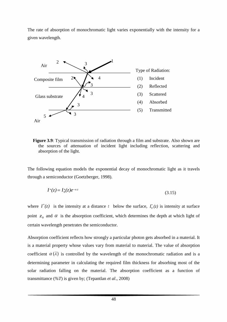
48
The rate of absorption of monochromatic light varies exponentially with the intensity for a
given wavelength.
Figure 3.9: Typical transmission of radiation through a film and substrate. Also shown are
the sources of attenuation of incident light including reflection, scattering and
absorption of the light.
The following equation models the exponential decay of monochromatic light as it travels
through a semiconductor (Goetzberger, 1998).
zα(z)eI(z)I 0 (3.15)
where (z)I is the intensity at a distance z below the surface, (z)I 0 is intensity at surface
point 0z and is the absorption coefficient, which determines the depth at which light of
certain wavelength penetrates the semiconductor.
Absorption coefficient reflects how strongly a particular photon gets absorbed in a material. It
is a material property whose values vary from material to material. The value of absorption
coefficient )( is controlled by the wavelength of the monochromatic radiation and is a
determining parameter in calculating the required film thickness for absorbing most of the
solar radiation falling on the material. The absorption coefficient as a function of
transmittance (%T) is given by; (Tepantlan et al., 2008)
Air
Composite film
Glass substrate
Air
1 3 2
2
3
5
4
4
3
3
3
Type of Radiation:
(1) Incident
(2) Reflected
(3) Scattered
(4) Absorbed
(5) Transmitted
(2)+(3)+(4)+(5)=(1)

49
Tz)λα(
%
100ln
1 (3.16)
where z is film thickness and T% is equal to 100 multiplied by the ratio of intensity of light
(I ) to the intensity of incident light (
0I ).
Small values of absorption coefficient ( )indicate weak absorption while large values of
indicate strong absorption of light in a material. The inverse of is known as absorption
length ( az ) and expressed as:
1az (3.17)
A requirement for solar cells is for film thickness ( z ) to be significantly larger than the
adsorption length to ascertain the quantitative light harvesting in the spectral absorption range
(Gratzel, 2005). High value of for a semiconductor represents high absorption probability
since only photons are involved in light absorption. Thinner solar cells can be fabricated from
direct band gap semiconductors because for high value of , only a small thickness in range
of a few micrometers is required to absorb relevant range of photons. It follows that the
thickness of the nanocrystalline film applied in DSSC is typically of the order of a few
micrometers in order to ascertain enhanced light absorption.
(b) Optical band gap (Eg)
In an intrinsic semiconductor, optical band gap indicates the region linking the top of the
valence band (VB) which is completely filled with electrons, and bottom of the conduction
band (CB) that is bare of electrons. Ideally, it is the energy range over which the density of
states is zero. The optical band gap is very large for insulators but nil for metals. The band
gap in semiconductors is typically intermediate between these two. The ability of a
semiconductor to absorb light from solar spectrum depends on the size of its band gap. To
examine the band gap of a semiconductor, light with variable photon energy near the band
gap is used. In such a case, light with lower energy photons does not get absorbed and light
with high photon energy is absorbed. The photon energy at which transition between
absorbing and non-absorbing behaviour takes place correspond to the optical band gap
energy. This transition between absorption and transmission is gradual and thus provides

50
information into some details of the transitions between energy states in valence band and
conduction band. The region of this transition is called absorption edge. It is difficult to
define the absorption edge experimentally due to formation of a tail in the absorption
spectrum (Li et al., 2009). As a result, the Tauc model has been devised as an empirical
model for measuring the optical band gap (Sanchez, 2014). The optical absorption edge in
semiconductors is analyzed using the Tauc model given in following equation (Tauc, 1966);
mg )EB(hαh (3.18)
where is absorption coefficient, h is Planck’s constant, is frequency, B is a
proportionality constant (band tailing parameter) taking values between 107 and 108 m-1
(Illican, 2008), gE is the optical band gap energy, and m is a constant that assumes values
m = ½ for direct band gap or m = 2 for an indirect band gap (Gould & Lamont, 2010). The
optical band gap energy ( gE ) for semiconductor thin films can be evaluated by considering
transition between valence band and conduction band when a photon of energy, h , falls on
the semiconductor.
i) For direct transitions, m = ½ and equation (3.18) becomes;
)EB(hαh g 2 (3.19)
The plot of 2αh versus h should be linear over a wide range of photon energies for
direct transition. The intercept of this plot on the energy axis gives the energy band gap ( gE )
(Swanepoel, 1983).
ii) For indirect band gaps: m = 2 and equation (3.19) becomes
2
g )EB(hαh (3.20)
Plotting versus 2h shows a linear dependence.
The photon energy is related to wavelength in (nm) according to;

51
(eV)(nm)λ
1240
λ
chhE (3.21)
From equations (3.20) and (3.21) the absorption coefficient )( of a material depends on the
wavelength of light incident. Since only light photons with gEh can excite electrons
across a materials band gap and contribute to solar cell performance, the band gap is
important in synchronizing a solar cell to solar spectrum.
(c) Urbach energy ( UE )
In optical absorption in a semiconductor, electrons get excited across the energy band gap
from the top of the valence band (VB) to the bottom of the conduction band (CB). If the
electrons encounter disorder during this transition, their density of states decrease
exponentially (tail off) into the energy gap away from CB. This tail of density of states
extending into the energy band gap is termed Urbach tail and the energy associated with it is
the Urbach energy. Swanepoel, (1983) and Caglar, (2006) reported that absorption coefficient
( ) near the band edge assume an exponential dependence on photon energy estimated by
following equation;
U0 Ehexpαα (3.22)
where UE is Urbach energy and 0 is a material dependent constant.
Thus, the Urbach energy can be estimated by plotting αln against photon energy )( h . The
linear part of the resulting curve can then be fitted with a straight line. The Urbach energy
equals the inverse of the slope. Thus the exponential band tailing can explain the observed
Urbach tail of the absorption coefficient versus photon energy. The values of Urbach energy
indicate the degree of structural disorder in a semiconductor. High UE indicates substantial
formation of tail states at the band margins.
(d) Refractive index (n)
The refractive index (n) of a material is defined as the ratio of speed of light in a vacuum to
phase velocity of light in the medium. The concept of refractive index is widely used with

52
components of the electromagnetic spectrum from radio waves to x-rays. The refractive index
varies with the wavelength of light and can be calculated from the measured transmittance
(T) and reflectance (R) using any of the following three equations: (i) equation (3.23) when
the absorption is high (ii) equation (3.24) when interferences are determined and (iii)
equation (3.25) when absorption is low and there are no interferences (Born & Wolf, 2005).
In the first case where the absorption is high and there is nil or minimal interferences,
Equation (3.23) was developed to calculate refractive index fn for thin films (Benno &
Joachim, 2003).
RRRn f 121 (3.23)
In the second case, where absorption of the film is negligible and interferences are
determined from the maxima in the transmission spectra, the refractive index ( sn ) of the thin
film-substrate can be derived by the following equation (Padera, 2013).
max
2
max11 TTns (3.24)
where Tmax is maxima in transmission spectra.
In the third case, where the absorption is low and there are nil or minimal interferences the
sample refractive index ( fn ) can be computed from the transmission minima (Tmin) by using
the following equation:
22
sf nMMn (3.25)
When light, an electromagnetic wave, propagates through a material, part of the light gets
attenuated. This attenuation can be accounted for by defining a complex refractive index
)(n
as follows;
kinn
(3.26)

53
where n is the real part and k is the imaginary part of the complex refractive index. In
addition, k is also known as extinction coefficient associated with the attenuation of light
passing through the material. In a material science, the properties of a composite material
(film) can be predicted using the rule of mixtures given in following expression: (Callister &
Rethwisch, 2010).
TNc nfnfn )1( (3.27)
where cn is the refractive index of composite film, f is the volume fraction of one of the
particles in the mixed-nanoparticle composite, Nn and Tn are refractive indices of the two
nanoparticles respectively.
(e) Extinction coefficient ( k )
The extinction coefficient ( k ) is the imaginary part of the complex refractive index and
measures the fraction of light lost due to scattering and absorption per unit distance in the
participating medium when an electromagnetic wave propagates through a material. Since all
components of electromagnetic waves or radiations travel in a vacuum at the speed of light,
c , the extinction coefficient can be related to the absorption coefficient ( ) according to
following equation (Yakuphanoglu et al., 2007):
44
v
ck (3.28)
The extinction coefficient ( k ) is zero when light travels through the material without loss,
whereas, k > 0 when light is absorbed. The extinction coefficient- depends on wavelength
(λ) of incoming light and on the intrinsic qualities of the material. A high extinction
coefficient is necessary for absorption of sunlight to make a good solar cell.
3.5 Electrical Characterization
Electrical characterization of thin films can be used to determine the electrical resistivity ( ),
sheet resistance ( sR ), conductivity ( ), Hall mobility ( H ), charge carriers density ( dn )

54
and type of charge carriers. The following sections give the theoretical foundations governing
the measurement of electrical properties by the Hall effect and the four point probe
techniques.
3.5.1 The Hall Effect
In 1879, Edwin Hall reported that when a magnetic field is applied transverse to the direction
of an electrical current in a conductor, an electric potential difference proportional to both the
magnetic field and the current is developed across the material in a direction perpendicular to
both current and potential (see Figure 3.10). This Hall Effect has been used to ascertain the
polarity of the moving charges that form the electric current. The Hall Effect measurements
are critical in electrical characterization of semiconductor materials and films because the
type of charge carrier, charge carrier density, and Hall mobility can be derived from the Hall
voltage. The many important applications of Hall Effect include position and motion
detectors, detection and measurement of magnetic fields for instance in cars electronic
ignition systems, and determination of type of charge carriers in semiconductor materials
(Pengra et al., 2014). For semiconductors, the particle size and band structure can give rise to
both negative (electron-like) or positive (hole) or absence of an electron) effective charge
carriers.
In equilibrium, the magnetic force ( BF ) equals to the electric force ( EF ) and for a conductor
of width l , the developed Hall Voltage ( HV ) is given by;
lBvlEV yxHH (3.29)
Where HE is the measured Hall electric field, xv is the average velocity of charge carriers,
and yB is magnetic field in the y direction.
The average velocity ( xv ) of charge carriers is obtained from (Jewett & Serway, 2010)
zlqnI
vd
xx (3.30)

55
where xI is the current through the sample, dn is the charge carrier density, )(q is the
elementary charge, l is the semiconductor width and z is the semiconductor thickness.
Figure 3.10: Arrangement for measuring the Hall voltage showing current in x-direction,
magnetic field in y- direction and Hall voltage measured in z-direction.(Jewett &
Serway, 2010).
(a) The Hall voltage (VH) and Hall coefficient (RH)
The Hall voltage (VH) can be obtained from equations (3.29) and (3.30) as:
z
BIR
zqn
BIV
yx
H
d
yx
H (3.31)
where RH is the Hall coefficient and given by
qnR
d
H
1 (3.32)
According to this equation (3.32), the Hall coefficient )( HR varies inversely with the number
of charge carrier density ( dn ). From equation (3.32), the Hall coefficient is expressed in
terms of measurable quantities according to;
z
I xv
F
B
y z
VH l
x

56
)C(cmBI
VzR
yx
H
H
13 (3.33)
Where VH is the Hall voltage measured along z-axis, xI is current, yB magnetic field and
z is the sample thickness.
The values of Hall voltage, current and magnetic field are measured using the Hall Effect
equipment. With known value of thickness (z), the Hall coefficients can be obtained from
equation (3.33).
(b) Charge carrier density ( dn )
Charge carrier density is an important electrical property of semiconductors typically
measured using the Hall Effect technique. Using equation (3.33), the number density of
charge carrier ( dn ) is evaluated from fundamental charge ( q ) and Hall coefficient )( HR
according to following equation 3.34:
)(cmqR
n -
H
d
31 (3.34)
The sign of Hall coefficient determines the type of charge carriers in the sample. It is
negative if majority charge carriers are electrons ( n type semiconductors), and positive if
charge carriers are holes ( p type semiconductors).
(c) Film resistivity
In a semiconductor, the electrical conductivity is determined by Hall mobility among other
factors. The electrical resistivity ( ) can be readily measured using the four point probe. For
a thin sample, film resistivity ( ) is expressed as:
)(2ln
11 cmzRzI
Vπρ S (3.35)
and )/(532.42ln
squareI
V
I
VπRS (3.36)

57
where Rs is the sheet resistance, V is voltage, I is current and z is sample thickness.
Electrical resistivity of the film is therefore the product of film thickness ( z ) and sheet
resistance ( SR ). As indicated in equation (3.36), the voltage becomes an indication of sheet
resistance if a constant current source is used. The sheet resistance influences the series
resistance of the cell. A low value of sheet resistance is preferred, but low sheet resistance
requires thicker layers causing reduced light transmittance and efficiency (Han et al., 2005).
The sheet resistance of semiconductor films can be measured using the four point probe
where two probes are used for current injection and the other two probes are used to measure
the voltage drop. The more usual probe geometrical configuration is when the four probes are
placed in a straight line (Deen & Pascal, 2006).
(d) Hall mobility H
The Hall mobility H is defined as product of Hall coefficient HR and electrical
conductivity ( ) according to:
σRμ HH (3.37)
Equation (3.37) can be used to determine the mobility of the charges in the deposited films.
3.6 Structural Characterization
The crystalline phase composition is analyzed using X-ray diffractometer (XRD). The x-ray
photons with energy typical of the target material are used. The photons are typically
displayed in the form of high intensity-characteristic peaks used for diffraction analysis.
When these x-rays are focused on a material, they get reflected by the atoms in specific
directions. The difference in path length of reflected beams must be an integral number of
wavelengths for maximum intensity according to Bragg’s law;
θdnλ hkl sin2 (3.38)

58
where λ is the x-rays wavelength, hkld is inter planar crystal spacing, and θ is the angle
made by incidence x-rays with crystal planes.
The process of reflection occurs when reflected beams are generated from at angle 2θ from
the incident beam. The shape of the unit cell determines the indices h,k,l that define the
possible d-spacing. i.e.,
hkldnλθ
2sin (3.39)
The highest electron densities are found around atoms. Thus, the intensities depend on the
type of atoms present in material and positions in the unit cell. Equation (3.39) is used in the
analysis of the diffraction patterns of the sample material and hence is used for elemental
identification and the kind of crystal orientation (Simiyu, 2010). The diffraction pattern of the
sample is obtained by plotting the X-ray intensity in a.u. on the y-axis and the measured
diffraction angle 2-Theta on the x-axis. The diffraction pattern consists of a series of peaks
which correspond to x-rays diffracted from a specific set of planes in the specimen. The
positions of peaks depend on the crystal structure of the material that enables the
determination of structure and lattice parameters of the material. The standard peaks and
intensities for materials can be obtained from databases of powder diffraction files (PDF)
such as that of the Joint Committee on Powder Diffraction Standards (JCPDS).
Experimentally obtained peaks may vary slightly from the standard ones and the main
variation arise from the peak broadening that is mainly caused by the size of the crystal and
the overlapping of the peaks.
Subsequent to optical, electrical, and structural characterization, the semiconductor films can
be chemisorbed with a dye thereby forming photoelectrodes to be used in a dye-sensitized
solar cell. The dyes inject electrons into conducting band of the films which in turn, conduct
the electrons to the external circuit resulting in an electric current (O’Regan & Gratzel, 1991).
Consequently, the assembled DSSCs are characterized to determine their performance.

59
3.7 Characterization of DSSCs
Dye-sensitized solar cells are usually characterized using photoelectric current-voltage (I-V)
measurements and curves. The photovoltaic parameters corresponding to I-V measurements
include short-circuit current density (JSC), fill factor (FF), open circuit voltage (VOC), and
efficiency ( ).
(a) The short circuit current density (JSC)
When a load is connected to a solar cell, a voltage develops across the terminals of the cell. A
solar cell is usually treated as a diode. The dark current density ( darkJ ) is given by following
equation, (Maluta, 2010)
empBdark Tk
qVJJ exp0 (3.40)
where 0J is the reverse bias saturation current density, q is elementary charge, V is the
voltage across the terminals, Bk is Boltzmann’s constant, empT is temperature.
The short circuit current density (JSC) is the current drawn when the terminals of the circuit
are connected together and therefore the applied voltage across the device is zero. The net
current density (J) can be attained from the difference between the short circuit current
density (JSC) and dark current density (Jdark):
1exp0
empBSCdarkSC Tk
qVJJJJJ (3.41)
The short circuit current (ISC) increases linearly with light intensity. It also depends on the
amount of the dye chemisorbed onto the semiconductor and on the electrochemical or
electrokinetic properties of the red-ox couple in the electrolyte.
(b) The open circuit voltage (VOC)
Photovoltage in a solar cell originate from the accumulation of electrons in metal oxide such
as TiO2 film. The open circuit voltage ( OCV ) is the voltage developed when the terminals of

60
the circuit are isolated (infinite load resistance) and is equal to the difference between the
Fermi level (FE ) of nanocrystalline semiconductor film and the electrochemical potential
( redoxV ) of the red-ox couple in electrolyte, i.e.,
redoxFOC ΔVEV (3.42)
In an n-type semiconductor with electrons as majority charge carriers, the Fermi level is near
the conduction band edge.
At the open circuit condition, Jdark = JSC, and open circuit voltage (VOC) is given by following
equation (Maluta, 2010);
1ln
0J
J
q
TkV SCempB
OC (3.43)
The equation (3.43) shows that OCV increases logarithmically with short circuit density (JSC)
and to reciprocal of the reverse saturation current ( 0J ).
(c) The fill factor (FF),
The fill factor (FF) is defined as the squareness of the IV-curve. It is therefore the ratio of
areas of two rectangles marked A and B shown in Figure 3.11. Fill factor measures the
ideality of the solar cell and is defined as the ratio of the maximum power output (ImaxVmax)
from the solar cell to the product of VOC and ISC ,i.e.,
BArea
AArea
VI
VI
VI
)(PpowerximummaFF
OCSCOCSC
maxmaxmax
(3.44)
where ISC is the short circuit current, VOC is the open circuit voltage, Pmax is the maximum
power, Imax is the current at maximum power, and Vmax is the voltage at maximum power. At
voltages below Vmax, the photocurrent through the external load is relatively independent of
output voltage (Figure 3.11). When voltage increases (> Vmax), recombination of increasing
number of charges takes place within the solar cells rather than the charges flowing in
external circuit through the load. At VOC, all charges recombine internally. Fill factor is

61
related to resistive losses in a solar cell. Theoretically, the best solar cell will have a
completely square I-V curve where FF =1. Such a cell will generate the same current
independent of the voltage.
Figure 3.11: Typical graph of solar cell’s output current (solid line) and power (dashed
line) as function of voltage. Also shown are rectangles A and B related to FF, the
cell’s short circuit current density (JSC), and open circuit voltage (VOC)
(Bowden et al., 2010).
In practice, however, no such level of squareness has been achieved. Some recent record FF
values of different material based solar cells are shown in Table 3.1. A Fill factor loss of
photon energy in solar cell arises due to series and shunt resistances of a cell. Ideally, the
series resistance should be low. High values of series resistance result in reduced short circuit
current ( SCI ) but not the open circuit voltage ( OCV ). Ideally, the values of shunt resistance
(RSH) should be very large (~ hundred ohms). Low values of shunt resistance affect the VOC
but ISC remains the same. It is difficult to minimize FF loss beyond its fundamental limit
Voltage (V)
JS
C
Ph
oto
cu
rren
t
den
sity
(m
A/c
m2)
VOC Vmax
Jm
ax
Pow
er (
mW
/cm
2) B
A
Pmax

62
Table 3.1: Recorded fill factor values of various types of solar cells (Green et al., 2017).
Material Record Fill Factor
Si (crystalline) 0.838
Si (multi crystalline) 0.800
GaAs (thin film cell) 0.865
CIGS (cell) 0.776
Dye-sensitized 0.712
Organic 0.742
Perovskite 0.723
(d) The solar cell efficiency ( )
The energy conversion efficiency ( η ) of the solar cell defines the percentage of solar light
converted to electrical energy. Mathematically, it can be obtained from the ratio of maximum
power ( maxP ) delivered at operating point to the incident power ( inP ). The light energy to
electric energy conversion efficiency ( η ) is expressed as;
)(
%10010022 cmmW P) Area (cm
FF (mW)VJ
powerlightincident
% outputPowerη (%)
in
OCSC
(3.45)
It follows from equation (3.45) that a high short circuit current ( SCJ ), a high open-circuit
voltage ( OCV ) and a fill factor ( FF ) close to 1 (or 100) are desirable for an efficient solar
cell.
3.8 Electrochemical Impedance Spectroscopy
In a dye-sensitized solar cell the electrons injected into semiconductor by the excited dye
upon light irradiation diffuse through the semi-conducting film. The electron transport within
the film encounters the diffusion impedance denoted by Rd (Cisneros et al., 2014). Other

63
internal impedances in a dye-sensitized solar cell include; (i) Nernstian diffusion related
impedance (Warburg) within the electrolyte (ii) the electron transport impedances in the
TiO2/electrolyte boundary, (iii) charge transfer related impedance at the platinum counter
electrode, and (iv) sheet resistance of the FTO (Shin et al., 2010). The term impedance refers
to frequency dependent resistance to current flow through a circuit elements such as resistors,
inductors or capacitors. In addition, the term electrochemical impedance is used in DSSCs
due to the cell’s specific hybrid character (Bisquert et al., 2000).
EIS measurements can be taken under any bias voltage and working conditions of the solar
cell. The most common approach adopted in EIS measurements involve applying a small-
amplitude sinusoidal voltage ),( tV over a wide range of frequency to an electrochemical
cell and measuring the corresponding sinusoidal current at open circuit voltage. The small-
amplitude excitation sinusoidal voltage ),( tV depends on time according to following
expression (Bisquert et al., 2000):
)(exp),( 0 tjVVtV OC (3.46)
where OCV is open circuit voltage, OV is amplitude of excitation voltage, and ω is the angular
frequency in radians per second. The AC signal is superimposed on a DC voltage at OCV bias
potential, resulting in a small-amplitude response alternating current signal ),( tI expressed
as function of time in form:
)](exp[),( 0 tjIItI OC (3.47)
where OCI is short circuit current, 0I is the amplitude, and ϕ is the phase angle through
which response signal shifted from the excitation signal.
The impedance ),( tZ of the system can be expressed in an equation derived in manner
similar to Ohm’s law as:
)sin(
)sin(
)sin(
sin
),(
),(),( 0
0
0
t
tZ
tI
tV
tI
tVtZ (3.48)

64
where 0Z is amplitude of impedance.
The smallness of amplitudes of both potential ),( tV and current ),( tI signals ensures
that ),( tZ is independent of the amplitude of the perturbation. The impedance ),( tZ can
then be expressed as a complex quantity because ),( tI contains magnitude as well as phase
information:
)()()sin(cos)( ///
0 jZZjZZ (3.49)
where cos)( 0
/ ZZ and sin)( 0
// ZZ are the real and imaginary and
components of the impedance, respectively and 1j .
(e) EIS data presentation
If the imaginary part of the impedance ( )(// Z ) is plotted on the y-axis and the real part
( )(/ Z ) on the x-axis, a Nyquist plot is obtained (Figure 3.12). A point on the Nyquist plot
represents the impedance, measured at a given frequency. When real component of
impedance is plotted against logarithmic frequency, the Bode plot is obtained (Bisquert &
Fabregat-Santiago, 2010).
Figure 3.12: A typical Nyquist plot and Bode plots resulting from projection onto /// ZZ plane and //Z plane for electrochemical system (Yavuz, 2014).

65
Bode plots explicitly show the frequency dependence unlike Nyquist plots. The semicircle on
a Nyquist plot is characteristic of a single time constant. High frequency data appear on left
hand side and low frequencies on the right side –positive real axis - of the Nyquist plot
(Figure 3.12). Measurements of impedance at low frequencies are useful in ensuring that one
approaches the DC regime. The arc in Nyquist plots characterize the time constants namely,
electron lifetime ( n ) and transit time ( t ), related to RC circuits from which Nyquist plots
result. Bode plots are frequently used to determine charge recombination time by the
maximum frequency calculations (Yavuz, 2014)
(f) EIS data analysis model elements
Interpretation of EIS data can be performed by the equivalent circuit modeling, which is a
method for fitting theoretical data to measured impedance data of an electrochemical device
(cell). The EIS data fitting models facilitates translation of internal processes occurring in the
device, including charge transport in the film, charge transfer (recombination) across
interfaces, and charge accumulation at certain points. The electrical circuits in the models are
typically built using (i) passive elements like resistors and capacitors, and (ii) distributed
elements such as constant phase elements ( CPE ) and Warburg impedance )( dZ . These
circuit elements can be arranged in series, parallel or their combination to build complex
equivalent circuits models for the given set of data and the Kirchoff’s laws applied (Autolab,
2012). Most impedance systems have data fitting programs useful for estimating model
parameters.
(g) Circuit element resistance
When frequency )( of applied perturbation is very low )0( , the conditions in a
system approximate those driven by a direct current and impedance )0(Z becomes equal to
DC resistance (DCR ), i.e.,
DCRI
VZ
)0()0(
)0( (3.50)
where )0(V is applied potential difference and )0(I is the current at very low frequencies.
The resistor’s impedance is thus unaffected by frequency and has zero phase difference.
Nyquist plot corresponding to a resistor becomes a vertical line. The ohmic resistance can be

66
obtained in a Nyquist plot at the junction of the impedance curve and the real impedance axis,
corresponding to very low frequency.
When frequency )( becomes high, certain procedures in the system become unresponsive
to the applied perturbation yet impedance must include contributions from such processes
(Bisquert & Fabregat-Santiago, 2010).
(h) Circuit element Capacitor
If we divide the change in electric charge )(Q by a voltage perturbation )(V , we obtain
a frequency-dependent capacitance )(C . The impedance (capacitive reactance) )(CZ of a
circuit element capacitance )(C , is given by:
CjZC
1 (3.51)
The capacitive impedance decreases as frequency increases and at very large frequencies
( , the capacitor becomes short-circuited (Bisquert & Fabregat-Santiago, 2010). On
the other hand, at very low frequencies ( 0 ) the capacitor can be substituted by an open-
circuit with total impedance equal to infinity. In this case, there is no dc current flowing in
the system as dc resistance is infinity. The constant phase element ( CPE ) rather than
capacitance is usually used in modeling where surface under investigation lack homogeneity
(Autolab Application Note, 2012)
(i) Constant phase element (CPE )
The impedance CPEZ relating to constant phase element (CPE ) is expressed as:
bCPE jAZ
)( (3.52)
where A is a constant and b is an integer (0 ≤ b ≤ 1). When b = 0 the CPE acts as an ideal
resistor, while it acts as an ideal capacitor when b = 1. When b = 0.5, the CPE is the
equivalent of the so-called Warburg element, described below.

67
(j) Warburg impedance )( dZ
Warburg impedance models the diffusion resistance of ionic species at the interface of ionic
species. The impedance of a diffusion layer is obtained from;
jYZd
0
1 (3.53)
where Y0 is the diffusion admittance. Warburg impedance contributes to phase change of 45°
since identical real and imaginary impedance contributions characterize it.
The equivalent circuit of transmission line model used to fit impedance spectra of dye-
sensitized solar cells is shown in Figure 3.13 (Jennings et al., 2012). In this figure, blocks
have been used to represent the TCO of photoelectrode, TiO2 film, electrolyte, and the
platinum-coated TCO of counter-electrode. The equivalent circuit shown in Figure 3.13 treats
each nanoparticle of the film as a resistive element coupled to the electrolyte through the
film/electrolyte interface (Gratzel, 2005).
Figure 3.13: Equivalent circuit of Transmission line (TL) model used to fit impedance
spectra of dye-sensitized solar cells (Sarker et al.,2014 ).
The elements of the equivalent circuit of transmission line model shown in the Figure 3.13
are defined as shown in following Table 3.2; (Fabregat-Santiago et al., 2005).

68
Table 3.2: The description of elements of the equivalent circuit of Transmission line (TL)
model (Fabregat-Santiago et al., 2005).
Elements of EIS Definition
SR Series resistance, accounting for charge transport resistance in the TCO glass;
z Thickness of the TiO2 film;
)( zrR tt Electron diffusion (transport) resistance between TiO2 nPs and TiO2 film and FTO
glass;
)( zrR rr Recombination resistance at the interface between the TiO2 film and the liquid
electrolyte;
)( zcC Chemical capacitance of the TiO2 film representing change of electron density as a
function of Fermi level;
dZ Warburg impedance representing the Nernst diffusion of tri-iodide species in the
electrolyte;
ptR Charge-transfer resistance at the platinized TCO glass counter electrode;
ptC Interface capacitance at the platinized counter electrode and electrolyte interface;
TCOR Charge-transfer resistance for electron recombination from uncovered layer of the
conducting glass (TCO) to electrolyte;
TCOC Capacitance at the triple contact TCO/TiO2/electrolyte interface.
The impedance function of the transmission line model is given by following expression:
(Fabregat-Santiago et al., 2005; Wang et al., 2005)
2
1
2
12
1
1coth
1rd
r
r
rt j
j
RRZ
(3.54)
where tR is the electron diffusion resistance, rR is the recombination resistance,
CRtd 1 is the characteristic frequency of diffusion and CRrr 1 is the rate
constant for recombination. The recombination resistance ( tR ) is sum of resistance between
the TiO2 nanoparticles and resistance between TiO2 film and the FTO glass substrate
(Bisquert et al., 2009). It can be calculated from:
rtott RRR 3 (3.55)

69
where totR is the total resistance of the cell.
The charge-transfer resistance ( ptR ) at the platinum counter electrode is associated with the
red-ox reaction involving
3/ II species (Wang et al., 2005). Low ptR values implies high
catalytic activity for reduction of the red-ox couple. The chemical capacitance ( C ) reflects
the density and distribution of the electronic sites in the band gap of the semiconductor (Li et
al., 2012).
The Warburg impedance ( dZ ) representing the Nernst diffusion of tri-iodide species in the
electrolyte is described by following expression (Fabregat-Santiago et al., 2011);
2
1
2
1
tanh
d
d
dd
j
j
RZ
(3.56)
where dR is diffusion resistance of ions in electrolyte and d is characteristic frequency of
diffusion.
The chemical capacitance )( C can be calculated as follows, (Rahman et al., 2015)
rr RωC
1 (3.57)
The electron diffusion coefficient (Dn) is obtained from (Adachi et al., 2006; Rahman et al.,
2015);
r
t
rn z
R
RD
(3.58)
where rR is recombination resistance, tR is electron diffusion resistance, z is film
thickness, and r is the rate of recombination.

70
If tR > rR the impedance of the diffusion-recombination follows the Gerischer impedance.
This is not desired in DSSC because the photoinjected electron will be lost through
recombination with the electrolyte before it reaches the TCO/TiO2 interface.
The diffusion length ( dL ) of electrons is a key parameter for enhancing conversion efficiency
in a DSSC and can be calculated according to
nnd DL (3.8)
The electron lifetime ( n ) within the film is calculated using following expression (Luo et
al., 2016);
max2
1
fn
(3.59)
where maxf is the maximum peak frequency. In Figure 3.14, recombination resistance rR is
represented by recR and frequency r represented by rec .
Electrochemical impedance spectroscopy (EIS) measurements can be conducted with the
instrument in potentiostatic mode and in combination with the frequency response analyzer
(FRA). In potentiostatic mode, potential is controlled and current measured. In EIS
measurements, the FRA module produces a small-amplitude sinusoidal wave with a user-
defined frequency (NOVA, 2016). This excitation signal and the applied DC voltage are then
superimposed on the cell. The response small-amplitude signal potential is then measured
using the FRA module and impedance ( Z ) computed. Both the real and imaginary parts of
impedance are computed together with phase angle shift between the excitation and response
signals. The frequency response analyzer (FRA) module produces three main equivalent
circuit elements; the series resistance (RS), parallel resistance (RP) and chemical capacitance
(Cμ) or constant phase element ( CPE ).

71
Figure 3.14: Characteristic Nyquist plot measured on a liquid electrolyte based DSSC
showing the angular frequency at top of the arc that corresponds to the electron
lifetime (Bisquert et al., 2009).
These circuit elements are related to combinations of the circuits elements shown in previous
Figure (3.13) for the transmission line circuit model. For example, the series resistance (RS)
represents the sum of TCO resistance, charge-transfer resistance at counter electrode, and
diffusion resistance in electrolyte, all of which produce a loss in the electrochemical potential
of the cell outside the active layer (Fabregat-Santiago et al., 2011; Luo et al., 2016).

72
CHAPTER FOUR
MATERIALS AND METHODS
4.0 Introduction
This chapter contains the experimental procedures for fabricating and characterizing both the
TiO2/Nb2O5 composite films and the dye-sensitized solar cell (DSSC). The films were
prepared using the electrophoretic deposition (EPD) method. Details on optimization of the
EPD process-parameters, characterization of both composite films and the fabricated solar
cell are presented.
4.1 Preparation of Transparent and Electrical Conducting Electrode
Commercially available transparent glass substrates (16 mm × 25 mm × 1 mm) coated with a
conducting layer of fluorine doped tin oxide TiO2 (FTO, F:SnO2) (Pilkington, Hartford Glass
Co. Inc., USA) having sheet resistances of 8 Ω/square were used as electrodes in EPD
technique. These FTO glass substrates were cut into smaller pieces (2.5mm2.0mm1.0mm)
and properly cleaned to remove contaminants and dust which could interfere with adhesion of
deposited film on the glass surface. The cleaning of the substrate included the following
steps: First, the FTO glass substrates were cleaned using detergent solution in a sonicator for
10.0 min. Secondly, the substrates were rinsed using distilled water. Finally, they were
sonicated in acetone for 10.0 min after which they were rinsed using distilled water in
ultrasonic bath. These glass slides were subsequently connected to EPD assembly as anode
and cathode for film deposition.
4.2 Preparation of the EPD Suspension
The experimental EPD suspension was created by dispersing commercial titanium dioxide
(TiO2) nanopowder (CAS No. 13463-67-7, Aldrich) and Niobium (V) oxide (Nb2O5)
nanopowder (CAS No. 1313-96-8, Acros Organics BVBA, Belgium), in 2-propanol (IPA:
Isopropyl alcohol) (Scharlau Chemie) contained in a Pyrex beaker. Varied amounts of both
TiO2 and Nb2O5 powders were weighed and poured into a Pyrex beaker containing 40mL of

73
V DC supply
Cathode
Anode
TiO2/Nb2O5_2-propanol
A
2-propanol to form the EPD suspension. In each case, the two metal oxide powders were
mixed in equal ratios (1:1). In addition, 5x10⁻⁵M magnesium nitrate hexahydrate pellets
(Mg(NO3)2·6H2O 99.9%, Aldrich) were weighed and added to the EPD cell to form an
electric charging system thereby controlling the zeta potential of the suspension as reported
by (Bandy et al., 2011; Lee et al., 2011). The suspension was then stirred for 30 minutes
using a power sonicator (Sonic 405) before it was used in the EPD equipment for film
deposition. The acidic (or basicity) levels of the suspension were determined by measuring
the pH values using a pH meter.
4.3 Electrophoretic Deposition of the TiO2/Nb2O5 Composite Films
The EPD apparatus included EPD cell (Pyrex glass beaker), DC power supply (Thurlby
Thadar TS30225), electrodes consisting of FTO coated glass substrates and equipment to
support the electrodes when partially immersed in the suspension. The EPD equipment was
set up as shown in Figure 4.1.
Figure 4.1: A schematic drawing of the EPD setup showing the two FTO coated glass
slides partially immersed into TiO2/Nb2O5_2-propanol suspension in a beaker. also
shown are the ammeter (A) and voltmeter (V) and applied DC voltage.
The FTO-coated glass substrate (cathode and anode) were arranged with conducting sides
facing each other in a parallel-plate configuration, separated by 1.2 cm, and partially
immersed in suspension made up of TiO2 and Nb2O5 powders, magnesium nitrate, and
74
2-propanol. A DC electric voltage of 35V was then applied across the electrodes for between
60s and 180s. A film was seen to form on the cathode implying that positive charges formed
on the surfaces of TiO2 and Nb2O5 particles when 2-propanol and magnesium nitrate were
used for the suspension. After the desired deposition time had elapsed, the film coated glass
substrate was slowly pulled out of the suspension thereby minimizing drag forces that could
affect quality of the film. The films were then annealed at 450°C for 6h with a heating rate of
5°C per minute. The furnace was then turned off and the substrate allowed to cool gradually
to room temperature (25°C).
Determination of (a) optimum mixing ratio of Nb2O5 and TiO2 and (b) the particle
concentration in suspension for film formation.
The mixing ratios (by mass) of solid in the suspension can play an important role for the
many component electrophoretic deposition (EPD). Then the particle concentration (g/L) of
nanoparticles for use in film formation was established. The following section 4.4 describes
the process of establishing optimum mixing ratios (by mass) of niobium (v) oxide and
titanium dioxide nanopowders i.e., TiO2:Nb2O5 used in film deposition. Section 4.5 outlines
the process of determining the particle/powder concentration (g/L) in fixed ratio for preparing
the EPD suspension.
4.4 Determination of optimum mixing ratio of Nb2O5 and TiO2 for Film Formation
The optimum ratio of Nb2O5 & TiO2 nanoparticles for use in fabricating the composite films
was determined from Hall effect measurements. The Hall Effect measurements involved
establishing the variation of the Hall voltage (VH) with particle concentrations of different
ratios of TiO2 and Nb2O5 particles in suspension. The optimum ratio of TiO2 and Nb2O5
particles forming film with largest Hall voltage was chosen. The optimum ratio was
maintained constant in all subsequent film depositions. Thus powder/particle concentrations
(g/L) were prepared by mixing fixed ratios of TiO2 and Nb2O5 particles but varying the
amounts (in g) of particles in suspension.

75
4.5 Optimization of Particle Concentration in EPD Suspension
Varied amounts (0.01 g to 0.03 g) of both TiO2 and Nb2O5 powders/particles at fixed mass
ratio established according to description in preceding section, were weighed and poured into
a Pyrex beaker containing fixed volume (40mL) of 2-propanol to form the EPD suspension.
5mM Magnesium nitrate hexahydrate (Mg(NO3).6H2O) was added into the suspension that
was then stirred for 30 min using a sonicator (Power Sonic 405). The electrodes were
partially immersed in the suspension and a DC voltage applied across them for specified
duration. The films deposited using varying particle concentrations were then annealed and
subjected to UV-Vis-NIR spectrophotometer for measurement of transmittance and
reflectance in wavelength range of 300 ≤ λ ≤ 3000 nm. The plots of transmittance and
reflectance versus wavelength were obtained. Transmittance data was analyzed and used to
plot transmittance versus particle concentration curves. From these curves, the particle
concentration that produced films of the highest transmittance were obtained.
4.6 Optimization of DC Applied Voltage for EPD
The suspensions with fixed particles ratio and concentrations (e.g., 0.25g/L: 0.25 g/L) for
TiO2 and Nb2O5 powders/particles in 2-propanol were prepared and used in determining the
optimum deposition voltage. Using the EPD method- the electrodes were partly dipped in the
EPD suspension and varying applied voltages ranging from 25V to 60V were applied for 90s.
The voltage was supplied by a DC dual faced power supply. The deposited films were then
subjected to transmittance measurements using UV-Vis-NIR spectrophotometer and graphs
of transmittance against wavelength plotted. The obtained transmittance data was then plotted
against voltage to determine the optimum applied voltage that produced films of the highest
transmittance at constant particle concentration and constant deposition time.
4.7 Optimization of Deposition Time for EPD
In order to optimize deposition time, the EPD suspensions of fixed particles ratio and
concentrations (e.g., 0.25g/L: 0.25 g/L) for TiO2 and Nb2O5 powders/particles in 2-propanol
were prepared and applied in film deposition for varied deposition times ranging from 60 s to

76
300 s. A constant applied DC voltage of 35V was applied across the electrodes partially
immersed in the suspension The deposited films were then subjected to transmittance
measurements using UV-Vis-NIR spectrophotometer. In this case the graphs of transmittance
against deposition times were plotted. The transmittance data was then plotted against time to
determine the optimum deposition time.
4.8 Measurement of Film Thickness
The Film thickness (z) was measured using surface profilometer. The films were then
subjected to electrical, optical, morphological and structural characterization.
4.9 Characterization of TiO2/Nb2O5 Composite Films Deposited by EPD Technique
Physical characteristics of the deposited TiO2/Nb2O5 composite films impact on the
performance of the dye-sensitized solar cell. The TiO2/Nb2O5 composite films deposited by
the electrophoretic technique were characterized using appropriate analysis techniques for
morphological, structural, electrical and optical properties.
4.10 Optical Characterization
Optical characterization of the TiO2/Nb2O5 composite thin films was carried out using
Shimadzu-DUV spectrophotometer. A baseline on spectrophotometer was recorded prior to
the measurement to calibrate the instrument. Spectroscopic transmission measurements of the
thin films were determined at normal incidence and at wavelengths in the range
nmnm 3200200 . Optical parameters like refractive index ( n ), extinction coefficient
( k ), dielectric constant ( ), optical band gap energy gE , and Urbach energy ( UE ) were
computed using primarily the Tauc equation and relevant equations discussed in chapter 3.

77
4.11 Electrical Characterization
The Hall Effect equipment and the four point probe were used to conduct electrical
characterization of the films. The electrical characteristics of a photoelectrode indicate the
suitability of a film in facilitating electron injection into and transport through the
photoelectrode. The following is a detailed description of application of Hall effect and four
point probe techniques.
(a) The Hall Effect measurement
The Hall Effect measurements involved measurements of the Hall voltage (VH) and current
(Ix) for constant applied magnetic field (By). The Hall voltage was measured in a
perpendicular direction to the magnetic field and to the direction of an electric current
flowing through the semiconductor using the configuration shown in Figure 4.2. The constant
direct-current and power supply meters were used to measure the supplied electric current (Ix)
and Hall voltage (VH) respectively.
Figure 4.2: Schematic drawing of Hall Effect measurement showing meters that provide
current and magnetic fields and clamp which support probes and the film.
The uniform magnetic field intensity (By) was measured using the digital flux/gauss meter
(Figure 4.2). Each sample was mounted individually onto a printed circuit, clamped and
attached to a stand placed between electromagnetic poles. The Hall voltage and current
values were measured and recorded for magnetic field of 3G (=0.0003T) at room temperature
Digital flux/
Gauss meter Constant direct
current supply
Film
Poles for
electromagnet
Film support
Power
supply

78
(25°C). The data and necessary equations were used to determine the Hall coefficients, type
of majority carriers, and charge carrier density in the semiconductor film.
(b) The Four point probe
The sheet resistance of the TiO2/Nb2O5 composite thin films was measured using the four
point probe, model SRM-232 (Figure 4.3). In a four-point probe, the four probes are placed in
a straight line. The voltage is measured across the inner probes while current is measured
across the outer probes. A four-point probe operates by passing a calibrated constant current
source of 4.53mA through the two outer tips (Figure 4.3). The probe was manually operated
by pressing the 4-point probe to the film. A current source was activated and the sheet
resistance (Rs) values measured and displayed on the 16 digit LCD front panel display. The
sheet resistance was used in equation (3.36) to determine the film resistivity (ρ).
Figure 4.3: Functional block diagram of SRM-232 four point probe showing four probes:
inner two for measuring voltage and outer two for measuring current.(After Bridge
Technology).
4.12 Morphological Characterization
The surface morphology of TiO2/Nb2O5 composite electrode thin films was investigated
using the scanning electron microscope (SEM) model S4100 HITACHITM to determine the
quality of the deposited films. No prior treatment was required before the scanning process
since all the films were coated on FTO glass substrate. The SEM images were taken at varied
magnifications that ranged from 000,1 to 000,30 and at a constant accelerating potential
of 5kV.
Current
probe Composite film
Voltage
probe
V
4.53 mA
Constant
Current
Substrate
V

79
4.13 Structural Analysis
Structural analysis of TiO2/Nb2O5 composite electrode thin films was conducted using
Shimadzu X-Ray Diffractometer with Cu Kα (k=15.418nm) radiation in the scanning range
of 2 from 0 to 80° to investigate crystalline material structure, including crystallite size and
atomic arrangement. For any particular Bragg angle (source and detector fixed), the specimen
was rotated such that the incident and diffracted beam made different angles to the specimen
surface (the angle between them remaining fixed at 2θ). The XRD pattern was analyzed using
the International Center for Diffraction Data (JCPDS card) (Feist & Davies, 1992; Frevel,
1955 (in Liu, et al., 2015)), Appendix A & B). Crystallite size is usually taken as the cube
root of the volume of a crystallite. The crystallite size (D) was examined from XRD peaks
based on the Scherer’s equation, (4.1).
θΔw
λ.D
cos940
(4.1)
where is the wavelength of X-ray radiation equal to 0.15406 nm for Cukα radiation, θ is
the Bragg’ diffraction angle, and Δw is the half-peak width of the X ray diffraction lines
(Khoby-Shendy et al., 2012). The half-peak width ( w ) is inversely proportional to
crystallite size (D). However, the half-peak width is difficult to calculate for many line X-ray
diffraction lines due to the dimensions involved.
4.14 Preparation of Components and Assembly of DSSCl
Subsequent to electrophoretic deposition of TiO2/Nb2O5 composite films, the films were
chemisorbed with dye and used to assemble the DSSC. The procedure for preparing the dye,
electrolyte and counter electrodes is described in the following subsection.
(a) Ruthenium dye staining of composite film
A synthetic Ruthenium-dye solution of 0.5 mM was prepared according to standard
procedure.

80
Ru-N719 whose chemical name is cis-diisothiocyanato-bis (2,2’-bipyridyl-4,4’-
dicarboxylato) ruthenium(II) bis(tetrabutylammonium) (CAS 207347-46-4) was purchased
from Sigma Aldrich and applied without further purification. The short formula for Ru-719
dye is RuL2(NCS)2:2TBA where (L=2,2’-bipyridyl-4,4’-dicarboxylic acid; TBA=tetrabutyl
ammonium). The dye solution was prepared by dissolving 6 mg of Ru-719 in 10 mL of
ethanol and sonicated until thoroughly mixed. The electrophoretically deposited TiO2/Nb2O5
composite films were preheated to 200.0°C for 10.0 minutes to remove adsorbed water. They
were then partially scrapped off to form an active area of 0.49 cm2. The films were immersed
into the dye solution whilst hot (~80°C) to prevent readsorption of water. The soaking of the
electrode in dye solution was maintained for 24 hours to enable proper dye chemisorption.
After the dye sensitization, the photoelectrodes were rinsed with ethanol to detach the
unabsorbed dye molecules after which they were immediately used as DSSC photoanodes.
(b) Preparation of the electrolyte
An electrolyte is required in a dye-sensitized solar cell to complete the circuit between the
sensitized photoelectrode and the counter electrode. In this work, an iodide/triiodide (
3/II )
red-ox couple based electrolyte prepared by dissolving: 0.101 g (0.04 M) iodine (CAS 7553-
56-2), 0.134 g (0.1M) lithium iodide (CAS 10377-51-2), and 1.477 g (0.5M) tetra-n-
butylammonium iodide, in 10 mL of acetonitrile (CAS 75-05-8) was used. Two drops of 4-
tert-butylpyridine (CAS 3978-81-2) were added to the electrolyte to augment the voltage
output in the same manner as described by Yang, (2011).
(c) Preparation of the Counter electrode
The platinum-coated counter electrodes (CEs) were fabricated by placing drops of 5 mM
hexachloroplatinic acid (H2PtCl6) (Fluka) on a cleaned FTO glass. The acid spread out evenly
covering the whole FTO-glass surface. The platinum film was obtained after heating the acid-
wet FTO glass at 450°C for 45 minutes and cooling the CE to room temperature. Presence of
platinum was confirmed by placing a drop of hydrogen peroxide on the glass slide resulting
in formation of bubbles.
(d) Assembling the dye-sensitized solar cell
The dye-sensitized TiO2/Nb2O5 composite photoelectrode was placed over platinum coated
counter electrode to form a sandwich arrangement. The edges of the cell were sealed by hot

81
pressing the two electrodes together with a 25-μm thick hot-melt gasket of Surlyn monomer
placed between them. The electrolyte containing iodine/tri-iodide red-ox couple was inserted
inside the sandwich arrangement via two small (0.5mm) holes drilled in the counter electrode
(CE). Consequently, the sealing of holes in CE was done using a small piece of microscope
covering plastic. The schematic diagram and photograph of assembled solar cell are shown in
Figures 4.4 and 4.5 respectively.
Figure 4.4: Schematic diagram of assembled dye-sensitized solar cell employing
TiO2/Nb2O5 composite electrode film.
Figure 4.5: Photograph of the assembled dye-sensitized solar cell based on TiO2/Nb2O5
composite electrode film showing predrilled holes through which electrolyte was
injected to cell.
FTO coated glass
substrate
FTO coated glass
counter electrode
(-)
(+)
Platinum layer
Surlyn
Spacer
Electrolyte
TiO2/Nb2O5 composite
film sensitized with N719
dye
Drilled holes for
injecting
electrolyte

82
4.15 Current-Voltage (I-V) Characterization of DSSC
The photoelectric current-voltage (I-V) characteristics of the cell were determined using a
digital source meter (Keithley-2400) under simulated sunlight of one sun. The simulated light
was provided by a solar simulator which closely approximates the solar radiation using the
light from a xenon ultra high pressure lamp through various filters. The currents and voltages
generated by the solar cell for diverse load resistances were measured under a set of standard
test condition for solar cells using the Keithley meter and computer (Jose et al., 2009). These
test conditions as outlined in international standards, e.g., ASTM E927-05 documents
essentially specify that the power density of the light illuminating the cell should be 100 mW
cm-2, temperature of 25°C, and the radiation condition should be AM 1.5 global for terrestrial
applications. The active area of the cell was 0.49 cm2.
The short-circuit current density (JSC), open-circuit voltage (VOC), fill-factor (FF), and energy
conversion efficiency ( ) were derived from the I-V curves and recorded. In addition, tables
with photovoltaic parameters for DSSCs employing electrophoretically deposited
photoelectrode for varied deposition time, applied voltage and particle concentration in
suspension were obtained.
4.16 Electrochemical Impedance Spectroscopy (EIS) Measurement of DSSC
The instrumentation required for EIS includes potentiostat, impedance analyzer and software
for data acquisition and analysis. Figure 4.6 shows the experimental set up for EIS
measurements on dye-sensitized solar cells (DSSC). The calibrated photodiode holder fitted
with two sliding clamps was used to fix the DSSC onto the holder. The cell was then
illuminated with red light (λ= 627nm) supplied by a light emitting diode (LED) powered by
Autolab LED driver (Figure 4.6). The spectra was obtained under 0.1 sun illumination at
0.5V direct current biasing. An AUTOLAB (PGSTAT204) equipment (Autolab, Switzerland)
in potentiostatic mode, connected to a computer was used to power the photodiode and the
LED driver. EIS -measurements were performed on the cell with the AUTOLAB instrument
joined with the frequency response analyzer (FRA32M) module. During the EIS
measurement, the FRA32M module (0.014V, 50Ω, 3906.9Hz) supplied a single-sine shaped
voltage of 5 to 15 mV. Upon application of a small-amplitude sinusoidal perturbation

83
potential of 10mV at fixed frequency, the sinusoidal current response was measured using the
NOVA software and the impedance at each frequency computed.
Figure 4.6: Electrochemical impedance spectroscopy measurement set up showing
Autolab connection to LED driver and the DSSC.
The measurements of impedance was repeated for frequencies supplied in the range of 10kHz
(highest applied) to 0.1Hz (lowest supplied). The frequencies were scanned at 5-10
measurements per decade. The biasing DC voltage of 0.5V was used in the EIS -
measurements because this value approximated the VOC of the fabricated solar cells. Open
circuit voltage is an important parameter in I-V characterization of solar cells. As such, the
impedances of the cells at biasing potential of around VOC was of interest. The real part and
imaginary parts of the impedance were then plotted to yield the Nyquist plot used to analyze
the solar cell. The results were then analyzed using the equivalent circuit as described in
following section.
The three main equivalent circuit elements; the series resistance ( SR ), parallel resistance
)( PR and chemical capacitance ( C ) or constant phase element ( CPE )were extracted from
EIS measurements under illumination at open circuit condition of 0.5V DC, by frequency
response analyzer (FRA) module coupled with NOVA software in Autolab instrument
(galvanometer). The EIS measurements were analyzed by fitting them with an equivalent
circuit constructed using various circuits elements provided in the NOVA software. NOVA
Computer LED Driver
AUTOLAB
PGSTAT204
cell
Photodiode holder
LED light

84
software analysis tools provides an electrochemical circle fit tool, that is used in estimating
the parameters of the equivalent circuit. For better fitting of theoretical data, all capacitor
elements were replaced by constant phase element (CPE or Q). Impedance data was fitted in
the electrochemical circle option using a predefined R(RQ) equivalent circuit. The
electrochemical circle option tool uses the measured data points of the circular portion of
Nyquist plot to calculate the values of the elements of the equivalent circuit. Electron
recombination lifetime ( n ) was estimated from maximum frequency values in Bode plot
using equation 3.59.

85
CHAPTER FIVE
RESULTS AND DISCUSSION
This chapter presents the experimental results and discussion related to (i) optimization of the
electrophoretic deposition (EPD) parameters, (ii) morphological, structural, electrical, and
optical characterization of the TiO2/Nb2O5 composite electrode thin films and (iii) the
current-voltage (I-V) and electrochemical impedance spectroscopy (EIS) characterization of
the fabricated dye-sensitized solar cell.
5.0 The pH and Optimization of Ratios of TiO2 and Nb2O5 Particles in Suspension
The TiO2/Nb2O5 composite electrode thin films were successfully deposited by
electrophoretic technique. Similar negative (-ve) charges formed on both TiO2 and Nb2O5
particles suspended in 2-propanol and contributed to film formation on EPD cathode
electrode (cathodic deposition). The pH values of suspension were found to influence the
deposition of nanocrystalline TiO2/Nb2O5 composite electrode thin films. For pH ≥ 5, the no
observable deposition took place after 3 minutes. Optimum pH for TiO2/Nb2O5 composite
thin films was 4.9, a value that was consistent with that (4.7) obtained by Teleki et al., (2006)
for deposition of nanocrystalline TiO2 film. Although each type of particle has same negative
charge developed on its surface, the particles could follow diverse deposition rates based on
the mass ratio of powders in suspension. Thus, optimization of mixing ratio by mass of the
powders was determined using Hall effect results.
Figure 5.1 shows a plot of Hall coefficients versus the increasing proportion of Nb2O5
forming ratio of Nb2O5 and TiO2 in suspension. The negative polarity of the Hall coefficient
values indicated that majority carriers in the TiO2/Nb2O5 composite films were n-type
(electrons). This polarity could have been caused by incorporation of Nb+5, and O-2 ions in
the composite. The bulk sized TiO2 is an n-type semiconductor due to presence of titanium
vacancies in TiO2 and due to oxygen vacancies which could be treated as donor type defects.
However, the many attributes of nanomaterials deviate from those of the same materials in
bulk. Niobium (v) oxide (Nb2O5) is reported to become an n-type semiconductor at lower

86
oxygen content. The Hall coefficient (RH) is known to be large for high Hall mobility of
charges (Jewett & Serway, 2010).
0.0 0.1 0.2 0.3 0.4 0.5 0.6 0.7 0.8 0.9-400
-300
-200
-100
0
100
200
300
Ha
ll co
effic
ien
t (
cm3/C
)
Proportion of Nb2O
5 particles in suspension (TiO
2 & Nb
2O
5)
Figure 5.1: Hall coefficient versus proportion of Nb2O5 by mass in suspension.
Proceeding from left to right of the figure, proportion of Nb2O5 increased while that of
TiO2 decreased. Films deposited using EPD technique using 35V, and deposition time
of 90s.
In preparation of suspension used to deposit the films of Figure 5.1, the mixing of
nanoparticles was carried out by increasing the proportion by mass of Nb2O5 (from 0.1 to 0.9)
while decreasing proportion of TiO2 (from 0.9 to 0.1). The largest value of absolute Hall
coefficient (RH) was obtained for proportion 0.45 (of Nb2O5) and 0.55 (of TiO2) in
suspension. For experimental purpose of measuring TiO2 and Nb2O5 by mass during the film
preparation, the ratio of 0.45: 0.55 was approximated to 0.5 : 0.5 or 1 : 1 (TiO2:Nb2O5).

87
5.1 Optimization of Concentration of TiO2 and Nb2O5 Particles in Suspension
Figure 5.2 shows plots of (a) transmittance against wavelength, (b) peak transmittance against
particle concentration and (c) film thickness against particle concentration for TiO2/Nb2O5
composite films.
0 500 1000 1500 2000 2500
0
15
30
45
60
75
90
(a)
(%)
Tra
nsm
ittan
ce
Wavelength (nm)
0.050g/L
0.125g/L
0.175g/L
0.250g/L
0.375g/L
0.500g/L
0.625g/L
0.750g/L
0.0 0.1 0.2 0.3 0.4 0.5 0.6 0.7
10
20
30
40
50
60
70
(b)
Pea
k (%
) T
rans
mitt
ance
Particle concentration in suspension (g/L)
0.0 0.1 0.2 0.3 0.4 0.5 0.6 0.7 0.8
0
1
2
3
4
5
6
7
8
9
10
(c)
Experimental
Theoretical (Hamaker's Eqn.)
Thi
ckne
ss (m
m)
Particle concentration in suspension (g/L)
Figure 5.2: (a) Variation of transmittance with wavelength, (b) variation of peak
transmittance with particle concentration and (c) film thickness versus concentration for
TiO2/Nb2O5 composite films deposited by EPD technique using applied voltage of 35V
and deposition time of 90s.

88
In preparing different particle concentrations, equal amounts (in g) of the nanopowders of
both Nb2O5 and TiO2 were mixed in 2-propanol thus maintaining a constant mass ratio of
1:1 in suspension for electrophoretic film deposition. In EPD preparation of each film,
deposition time of 90 s and the applied DC voltage of 35V were used. The concentration of
TiO2 and Nb2O5 particles ranged from 0.05 g/L to 0.75 g/L. From Figure 5.2a, it is observed
that the deposition of nanostructured TiO2/Nb2O5 composite film reduced transparency of
the conducting electrode (FTO) over near-infrared and the entire visible region of solar
spectrum. Plain FTO coated glass (0 g/L) had the highest transmittance (~ 80%). Further it
can also be seen in Figure 5.2a that peaks of maximum transmittance decreased and shifted
towards the long wavelengths region as the particle concentration in suspension, used for
films deposition, was increased. This shifting and reduction of peaks could be explained in
terms of reduction of photon energy )( h ,
chhE (5.1)
through the absorption of some photons in the composite film through which they traversed.
Thus, the transmitted photons had reduced energy (and large wavelength) leading to the
spectral shift. Thicker films obtained for higher particle concentrations were responsible for
greater reduction of the energy of the photons transmitted through them than did the thinner
films (Figure 5.2c). Thus the energy of transmitted photons reduced in thicker films which
accounts for the shift in maximum transmittance peaks towards longer wavelengths. Figure
5.2b shows the variation of peak transmittance with particle concentration is, while Figure
5.2c shows the variation of the film thickness with particle concentration. From Figure 5.2c,
it is noted that thickness of the films increased with particle concentration. Thus the decrease
of transmittance with particle concentration is due to the increase in thickness of the films
and hence absorption. Light transmission through a thick film experiences enhanced
attenuation. These findings were consistent with observations of Miyasaka and Kijitori,
(2004) that high particle concentration leads to particle aggregation in the deposited film.
Hamaker’s equation;
tCVm 5.2
with the proportionality constant, 11140701.0 sVKgm showed that the predicted film
thicknesses (mass/area) of the composite films varied linearly with increasing particle

89
concentration. The experimentally obtained thicknesses were slightly higher than the
theoretically obtained thicknesses. The difference in thicknesses was attributed to possible
non ideal stability of suspension with tendency to settle down unlike the prediction by
Hamaker’s equation. Although films deposited from concentrations less than 0.25 g/ L
produced high transmittances, they barely formed films of any appreciable thickness useful
for dye adsorption for application in DSSCs. Visual inspection showed that the films
corresponding to 0.25 g/L concentration had the best quality and cracks free films. Thus, 0.25
g/L was chosen as optimum EPD particle concentration for film preparation.
5.2 The Optimization of Deposition Time
Figure 5.3 shows plot of (a) transmittance versus wavelength, (b) peak transmittance versus
deposition time and (c) film thickness versus deposition time for TiO2/Nb2O5 composite films
deposited by EPD technique at applied voltage of 35 V and particle concentration of 0.25 g/L
in the suspension of 2-propanol. The peaks of maximum transmittance decreased and shifted
towards the long wavelengths region for films deposited using increased EPD deposition
time. This reduction and shifting could be attributed to reduced energy (and large
wavelength) of the transmitted photons resulting from absorption of part of the energy by the
film.
The variation of peak transmittance with deposition time is shown in Figure 5.3b while the
variation of film thickness with deposition time is shown in Figure 5.3c. It is noted, from
Figure 5.3c, that thickness of the films increased with deposition time. Thus, the decrease of
transmittance with deposition time is due to increase in thickness of the films and hence light
absorption. The typical TiO2 film layer thickness for DSSCs range between 5 and 15μm
(Jarernboon et al., 2009). The TiO2/Nb2O5 composite films electrophoretically deposited for
90 s (5.5 m ), produced the highest transmittance of 53% at λ = 1300 nm. In addition, the
best quality films from visual inspection correspond to deposition time of 90s. Figure 5.3c
shows the variation of thickness with deposition time for the composite films
electrophoretically deposited at 35 V and 0.25 g/L. According to theoretical (Hamaker’s
equation) prediction of film thickness formation, the thickness varied linearly with deposition
time. The equation assumes complete stability of suspension which shows no tendency to

90
settle down. The slight deviation from predicted linear relationship was attributed to
suspension instability.
0 500 1000 1500 2000 2500 3000
0
10
20
30
40
50
60
40 60 80 100 120 140 160 1800
1
2
3
4
5
6
7
8
9
10
60 80 100 120 140 160 180
10
20
30
40
50
60
Wavelength (nm)
60s
90s
120s
150s
180s
(a)
Experimental
Theoretical (Hamaker's Eqn.)
(c)
Deposition time (s)
(b)
Thic
knes
s (m
m)
(%) T
rans
mitt
ance
Peak
(%) T
rans
mitt
ance
Deposition time (s)
Figure 5.3: (a) Variation of transmittance with wavelength, (b) variation of peak
transmittance with deposition time and (c) thickness versus deposition time for
TiO2/Nb2O5 composite films deposited by EPD technique at applied voltage of 35V
and particle concentration of 0.25g/L in 2-propanol suspension.

91
5.3 Optimization of Applied Voltage
Figure 5.4 shows plots of (a) variation of transmittance with wavelength, (b) variation of peak
transmittance with applied voltage, and (c) variation of film thickness with applied voltage
for TiO2/Nb2O5 composite films deposited by EPD method using particle concentration of
0.25g/L and deposition time of 90s.
0 500 1000 1500 2000 2500 30000
10
20
30
40
50
60
20 25 30 35 40 45 50 55 6015
20
25
30
35
40
45
50
55
20 25 30 35 40 45 50 55 60 65
-2
0
2
4
6
8
10
12
14
16
(a)
(%) T
rans
mitt
ance
Wavelength (nm)
25V
35V
45V
55V
Pea
k (%
) Tra
nsm
ittan
ce
Applied voltage (V)
(b)
(c)
Thic
knes
s(m
)
Applied voltage (V)
Experimental
Theoretical (Hamaker's Eqn.)
Figure 5.4: (a) Variation of transmittance with wavelength, (b) variation of peak
transmittance with applied voltage, and (c) thickness versus applied voltage for
TiO2/Nb2O5 composite films deposited by EPD method using particle concentration of
0.25g/L and deposition time of 90s.

92
Transmittance was measured for composite films electrophoretically deposited at varied DC
voltage in the range 25 V to 60 V. It can also be seen in Figure 5.4 that peaks of maximum
transmittance decreased for films fabricated using increased values of EPD applied voltage.
In addition, the peaks of maximum transmittance shifted towards the long wavelengths region
as the applied voltage for films fabrication was increased. This shifting was attributed to the
reduced energy (and large wavelength) of transmitted photons since part of their energy was
absorbed by the film. The films deposited using higher EPD voltages had low transmittance
which could have resulted from increased absorption of light that travelled through the
thicker films. Thus the energy of transmitted photons reduced in thicker films which accounts
for the shift in maximum transmittance peaks towards longer wavelengths.
The variation of peak transmittance with applied voltage is shown in Figure 5.4b while
Figure 5.4c shows the variation of film thickness with applied voltage. From Figure 5.4c, it is
noted that the thickness of films increased with increasing applied voltage. Thus, the decrease
of transmittance with applied voltage was due to increase in thickness of the films and hence
increased absorption of light as it travelled through the thicker films. These results were
consistent with observation by Boccacini, (2010), that high voltages produce agglomeration
of particles resulting in thicker films. Figure 5.4c also shows variation of theoretically
determined film thicknesses with applied voltage.
The Hamaker’s Equation was used to fit the thicknesses. The apparently large divergence
between the experimental and theoretical results at large ( ≥ 35V) was attributed to greater
throwing power of high applied voltages thus higher thicknesses. Consequently, the applied
voltage of 35V corresponding to highest transmittance (53%), (Figure 5.4b) was chosen as
the optimum applied DC voltage for deposition of TiO2/Nb2O5 composite thin films. Table
5.1 shows the summary of the optimum EPD process parameters, namely DC applied voltage,
deposition times and particle concentrations. Even for electrophoretic deposition of TiO2
only, many different EPD process parameters have been used by other authors (Yum et al.,
2005; Kim et al., 2007; Bandy et al., 2011) as was shown previously in Table 2.1. It is clear
that there are no unique process parameters for film deposition by EPD technique. That is
why it is important to obtain the best deposition parameters in every situation. Composite
films deposited using these optimized EPD process parameters were used in fabrication of the
dye-sensitized solar cells in this study.
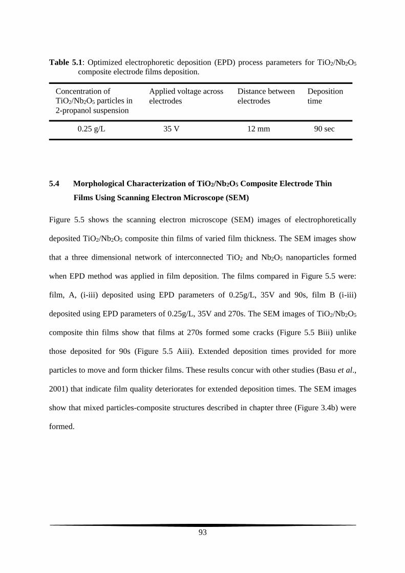
93
Table 5.1: Optimized electrophoretic deposition (EPD) process parameters for TiO2/Nb2O5
composite electrode films deposition.
5.4 Morphological Characterization of TiO2/Nb2O5 Composite Electrode Thin
Films Using Scanning Electron Microscope (SEM)
Figure 5.5 shows the scanning electron microscope (SEM) images of electrophoretically
deposited TiO2/Nb2O5 composite thin films of varied film thickness. The SEM images show
that a three dimensional network of interconnected TiO2 and Nb2O5 nanoparticles formed
when EPD method was applied in film deposition. The films compared in Figure 5.5 were:
film, A, (i-iii) deposited using EPD parameters of 0.25g/L, 35V and 90s, film B (i-iii)
deposited using EPD parameters of 0.25g/L, 35V and 270s. The SEM images of TiO2/Nb2O5
composite thin films show that films at 270s formed some cracks (Figure 5.5 Biii) unlike
those deposited for 90s (Figure 5.5 Aiii). Extended deposition times provided for more
particles to move and form thicker films. These results concur with other studies (Basu et al.,
2001) that indicate film quality deteriorates for extended deposition times. The SEM images
show that mixed particles-composite structures described in chapter three (Figure 3.4b) were
formed.
Concentration of
TiO2/Nb2O5 particles in
2-propanol suspension
Applied voltage across
electrodes
Distance between
electrodes
Deposition
time
0.25 g/L 35 V 12 mm 90 sec

94
Figure 5.5: SEM images of TiO2/Nb2O5 composite films electrophoretically deposited on
FTO glass slide from suspension in 2-propanol at 35V from 0.25g/L. film A: deposition
time of 90s, film B: deposition time of 300s. The films were annealed at 450°C for 6h.

95
5.5 Structural Characterization of TiO2/Nb2O5 Composite Electrode Thin Films
Using X-Ray Diffraction Analyzer
The crystal structure of TiO2/Nb2O5 composite thin films was investigated by X-Ray
Diffractometer using CuKα )41.15( nm radiation. Figure 5.6a shows the X-RD patterns
for TiO2/Nb2O5 composite film electrophoretically deposited at applied voltage of 35 DCV,
for 90 s from particle concentration of 0.25 g/L. The diffractograms were recorded in the 2-
Theta range of 10 - 80° and analyzed using the International Center for Diffraction Data
(JCPDS card) (Feist and Davies, 1992; Frevel, 1955 (in Liu, et al., 2015)). In addition, X-RD
graphs of TiO2 films (Figure 5.6b) and Nb2O5 films (Figure 5.6c) are shown for comparison.
The Diffraction peaks corresponding to films exhibit crystalline phases of both TiO2 (2θ =
25.5, 33.8, 37.9 & 51.5) degrees and Nb2O5 (2θ= 26.5, 34.5, & 52.6) degrees. The dominant
peak of TiO2 was at 2-theta of 25.5 deg while that of Nb2O5 was at 26.5 deg. The diffraction
peaks confirmed the presence of both titanium dioxide and niobium (v) oxide particles in the
TiO2/Nb2O5 composite film. Applying Scherer’s equation (4.1), the average crystallite sizes
at these peak positions were 15.36 nm and 15.49 nm and hence the crystallite dimensions
were confirmed to the nanoscale.
However, the peak (= 1,600 a.u.) of TiO2 was longer than that of Nb2O5 (= 900 a.u) which
translates to ratio 1.78:1. The length of peaks corresponds to degree of crystallinity (Chang et
al., 2009). It follows, therefore, that the crystallinity of TiO2 was higher than that of Nb2O5.
The intensity peaks were identified from standard JCPD diffraction data for TiO2 and Nb2O5
shown in appendix II.
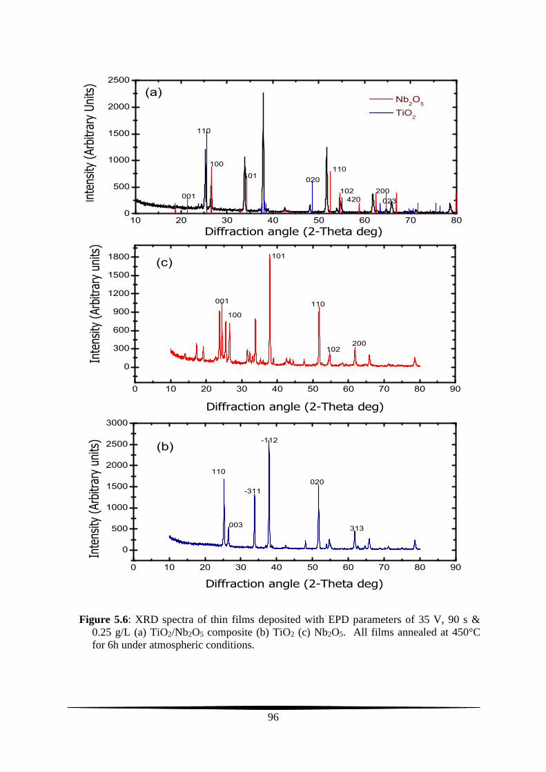
96
10 20 30 40 50 60 70 800
500
1000
1500
2000
2500
0 10 20 30 40 50 60 70 80 90
0
300
600
900
1200
1500
1800
0 10 20 30 40 50 60 70 80 90
0
500
1000
1500
2000
2500
3000
Inte
nsity
(Arb
itrar
y U
nits
)
Diffraction angle (2-Theta deg)
Nb2O
5
TiO2
001
110
100
101110
102 200
020
420 023
(a)
Inte
nsity
(Arb
itrar
y un
its)
Diffraction angle (2-Theta deg)
110
102200
101
100
001
(c)
Inte
nsity
(Arb
itrar
y un
its)
Diffraction angle (2-Theta deg)
110
003
-311
-112
020
313
(b)
Figure 5.6: XRD spectra of thin films deposited with EPD parameters of 35 V, 90 s &
0.25 g/L (a) TiO2/Nb2O5 composite (b) TiO2 (c) Nb2O5. All films annealed at 450°C
for 6h under atmospheric conditions.

97
5.6 Evaluation of Optical Band Gap Energy (Eg) of TiO2/Nb2O5 Composite Films
Figure 5.7 shows plot of 2)( h versus photon energy ( h ) for evaluating band gap of
TiO2/Nb2O5 composite thin films, and pure TiO2 and pure Nb2O5 thin films. The linear
variation of 2)( h versus h at the absorption edge indicates direct transitions took place
across the band gap of the material (Gould & Lamont, 2010). The optical band gap energy
(Eg) was estimated by drawing a tangent to the linear part of the curve and extrapolating the
tangent to intercept the h - axis.
1.5 2.0 2.5 3.0 3.5 4.0 4.5
0.0
0.2
0.4
0.6
0.8
1.0
1.2
1.4
1.6
1.8
Energy (h (eV)
(h)2
(eV/c
m)2
x10
-13
TiO2 (a)
Nb2O
5 (b)
TiO2/Nb
2O
5 (c)
(c)
(b)
(a)
Figure 5.7: Variation of 2)( h versus photon energy ( h ) for direct band gap
transitions in TiO2 (a), Nb2O5 (b) and TiO2/Nb2O5 (c) composite films at particle
concentration of 0.25g/L all the films were deposited using EPD technique at 35V,
0.25g/L, and 90s.
All films were deposited using the same EPD process parameters; i.e., applied voltage (35 V),
particle concentration (0.25 g/L) and deposition time (90 s). Band gap energies gE =3.932 eV
for pure Nb2O5, gE = 3.884eV for pure TiO2 and gE = 3.858 eV for TiO2/Nb2O5 composite

98
films were obtained. It follows that band gap energy obtained experimentally for the
composite film was lower than those obtained for pure TiO2 and pure Nb2O5. This decrease in
energy band gap for composite film was explained in terms of development of sub-band gap
states in the TiO2/Nb2O5 composite films. These sub-band gap states lie deep in the tail of the
density of states in the films and lead to decreasing the optical energy gap and shifting the
absorption edge towards the higher wavelength of the incident photons. The theoretical direct
band gap value of TiO2 is gE = 3.25 eV (Nowotny et al., 2008) and for Nb2O5 is gE = 3.49
eV (Jose et al., 2009). Thus, values of energy band gaps obtained experimentally for both
TiO2 and Nb2O5 were greater than the corresponding theoretical values. It is noteworthy that
the band gap from Tauc equations and corresponding plots were estimates and that the slope
of the absorption edge could have been affected by defects in the crystals.
Table 5.2, shows a comparison of band gap energies for TiO2 determined in this study with
those reported in literature. It is observed that the measured gE values lie in the range
3.25eV to 4.14 eV of the reported gE values.
Table 5.2: Values of direct and indirect optical band gaps of TiO2 and Nb2O5 reported by
various authors.
TiO2 3.25 NA Jose et al., (2009)
3.88 NA Narayan & Raturi (2012)
4.14 3.4 Ghrairi & Bouaicha (2012)
3.88 NA Yavuz, (2014)
3.5-3.9 2.1-3.0 Oommen et al., 2012
3.93 NA in this Study
Nb2O5 3.49 NA Sancho-Paramon, et al., (2008)
3.9 NA Parakh & Garg (1985)
3.75 NA Kovendlan et al., (2011)
NA 3.4 Yan et al., (2012)
3.86 NA In this Study
TiO2/Nb2O5 3.88 NA In this Study
NA ≡Not available
Eg (eV)
(indirect) Type of Thin
film
Eg (eV)
(direct) Reference

99
These results support the position that the band structure of nano-materials is greatly deviated
from their bulk counterpart (Jose et al., 2009).The condition that must be met for good
performance of a dye-sensitized solar cell is that the conduction band (CB) edge in
semiconductor has to match the lowest unoccupied molecular orbital (LUMO) of the excited
dye molecule to enable effective electron injection from the molecule’s excited state to the
semiconductor’s CB (Maluta, 2010). If the conduction band is lower in energy than the
excited state of the dye molecules, electron injection from the dye into the CB is good. On the
other hand, if CB is higher in energy, the electron injection is suppressed. The suppression of
electron injection contributes to low currents in the cells resulting in low conversion
efficiencies.
5.7 Effect of Annealing Time on Optical Band Gap of Composite Films
Figure 5.8 shows the plot of 2)( h against the photon energy h for TiO2/Nb2O5
composite films. The effect of annealing (dwelling) time on optical band gap was studied by
annealing the TiO2/Nb2O5 composite thin films at 450°C for different dwelling times between
1 and 6 hours. All the films were deposited using electrophoretic technique for deposition
time of 90 s, applied voltage of 35V, and from particle concentration of 0.25g/L.
Values of the measured band gap energies were recorded in Table 5.3. The optical band gap
of the as-deposited (un-annealed) film was found to be 4.063eV (Figure 5.8) which was a
value higher than any value of the annealed films. The decrease in band gap upon annealing
of films could be attributed to improved crystalline structure of the TiO2/Nb2O5 composite
films with increase in annealing temperature (from room temperature to 450°C).
The lowest states in conduction bands are localized (traps) due to the disordered arrangement
of the films deposited at low temperature (Matthew et al., 2012). These localized states make
the absorption edge shift to a higher energy. The crystallinity of the films was discussed
previously using XRD graphs (Figure 5.6) which show the intensity peaks with their width
for specific crystalline regions within a material. After annealing at 450°C for between 1 and
6 hours, the band gap decreased from 3.891eV for films annealed for 1 hour to 3.797 eV for
similar films annealed at same temperature for 6 hours.

100
2.6 2.8 3.0 3.2 3.4 3.6 3.8 4.0 4.2 4.4
0.0
1.5
3.0
4.5
6.0
7.5
9.0
10.5(
h)2
(eV/c
m)2x1
01
2
Photon energy (h (eV)
1h
2h
3h
4h
5h
6h
un annealed
Figure 5.8: Variation of 2)( h with photon energy )( h for direct transitions in
TiO2/Nb2O5 composite films deposited using electrophoretic technique using 35V,
0.25g/L, for 90s and annealed for 1 to 6 hours.
Table 5.3: Band gap energies for TiO2/Nb2O5 composite films annealed at 450°C for
different annealing times between 1 and 6 hours.
1 3.8911
2 3.8520
3 3.8515
4 3.8319
5 3.8315
6 3.7965
As-deposited 4.0633
The variation of band gap energies with annealing (dwelling) time is shown in Figure 5.9. It
was observed that the band gap energy values decreased linearly with increased annealing
Annealing
(dwelling) time (hrs)
Band gap energy
(eV)

101
time intervals. Decrease in band gap for increased annealing time has also been reported in
literature (Sanjeev & Kekuda, 2015). The narrowing of band gap could have resulted from
decrease in transitions due to reduction of the oxygen defect width as a result of air annealing
which fills up the vacant oxygen levels.
1 2 3 4 5 6
3.76
3.78
3.80
3.82
3.84
3.86
3.88
3.90
3.92
3.94
Band g
ap e
nerg
y (e
V)
Annealing time (hrs)
Figure 5.9: Band gap energy versus annealing time for TiO2/Nb2O5 composite thin films
annealed at 450°C for different annealing (dwelling) times between 1 and 6 hours. The
films were deposited using the EPD technique from 0.25g/L, 35V, and 90s.
5.8 Evaluation of Urbach Energy
The values of Urbach energy were calculated from the plot of )(ln versus photon energy
( h ) for the TiO2/Nb2O5 composite films (Figure 5.10). The plot is governed by equation
(3.23);
U0 Eh)(αlnαln )( (5.2).
The reciprocal gradient of the linear portion of the curve was used to calculate the Urbach
energy and a value of 434meV was obtained. The values of EU can be used to measure

102
structural disorder in the prepared samples. The Urbach energy value of 434meV indicated
that there was considerable introduction of tail states at the band edges thus influencing the
electron transport in the film. Increase in annealing time is known to restrict the shuffling
motion of atoms in composite films. Such limited motion could have contracted the Urbach
tailing thus lowering the EU, due to reduced number of vibrational energy levels for a given
electronic state.
0.5 1.0 1.5 2.0 2.5 3.0 3.5 4.0 4.513.5
14.0
14.5
15.0
15.5
16.0
Ln(
)
Energy, h (eV)
Figure 5.10: Variation of )(ln with photon energy for 522 / ONbTiO composite thin
films prepared using electrophoretic deposition technique. using 0.25g/L, 90s and 35V
and annealed at 450°C for 6h
The value of Urbach energy obtained in the study compares closely with 455eV for ZnO thin
films obtained by Yakuphanoglu et al., (2007). The obtained value of EU was within the
range (460 to 660 meV) for semiconductors reported by Sta et al., (2014). The Urbach energy
value of 434meV obtained in this study was significant in indicating the introduction of tail
states at band edges that influence electron transport.
5.9 Extinction Coefficient
Figure 5.11 shows the plot of absorption coefficient α )( against inverse of wavelength
(1/λ) for TiO2/Nb2O5 composite thin films in the wavelength range 400 ≤ λ ≤ 700nm (visible

103
light region). The slope of Figure 5.11 was used to calculate the value of extinction
coefficient ( k ), and an average value of k = 0.0354 at 400 ≤ λ ≤ 700nm for fabricated
TiO2/Nb2O5 composite thin films was obtained.
0.0015 0.0018 0.0021 0.0024 0.0027
1.7
1.8
1.9
2.0
2.1
2.2
2.3
Abso
rption c
oef
fici
ent
(cm
-1) x
10
5
Inverse of wavelength,1/ (nm)-1
Figure 5.11: Variation of absorption coefficient )( versus inverse of wavelength for
TiO2/Nb2O5 composite films deposited using EPD technique at 35v, 0.25g/L, and for
90s and annealed at 450°C for 6h.
The extinction coefficient ( k ), is an optical property of the semiconductor material and
determines how much light is absorbed by the material. Light is absorbed when k > 0, while
light travels straight through the material when k = 0. In this study, a value of 0.0354 was
obtained for extinction coefficient ( k ) which was attributed to low absorption of light by the
TiO2/Nb2O5 composite electrode thin films due to their large energy band gap. The results are
consistent with the knowledge about high band gap semiconductors that cannot require
sensitization with a dye to function as photoelectrodes in a dye sensitized solar cells

104
5.10 Evaluation of Refractive Index ( n )
Refractive index is associated with refraction of light passing through a material. The
absorbance of TiO2/Nb2O5 composite thin films was plotted against wavelength in the range
200 to 2800 nm (Figure 5.12). Absorbance is the capacity of a material (film) to absorb light
of a specified wavelength.
0 400 800 1200 1600 2000 2400 2800
0.4
0.5
0.6
0.7
0.8
0.9
1.0
Abso
rbance
Wavelength (nm)
Figure 5.12: Absorbance spectrum: values calculated from transmittance and reflectance
data for TiO2/Nb2O5 composite thin filmsdeposited by EPD method at 35V, 0.25g/L,
for 90s and annealed for 450°C for 6h.
As shown in Figure 5.12, the absorbance by the composite film is non-uniform as a function
of wavelength; with some regions showing low and others showing high absorbance. Simlar
phenomenon has also been reported by other authors (Born & Wolf, 2005). In the region
corresponding to wavelength range 400 ≤ λ ≤ 800nm in the absorption spectrum, the
absorbance was fairly constant (0.65) and therefore equation (5.3):
)1(/)21( RRRn (5.3)
was applied to evaluate refractive index ( n ) over the corresponding spectrum region.

105
The refractive index of 643.1n was obtained for wavelengths between 400 nm and 800 nm
(Figure 5.12). Different values of refractive indices have been reported by authors like
Hosaka et al., (1997), who obtained refractive index equal to 2.55 for TiO2 at nm600 .
Mandic (2015) also reported refractive index 493.2n for TiO2 at nm8.632 . At
nm550 the refractive index of TiO2 films annealed at 600°C was 2.11 (Matthews et al.,
2009). The refractive index ( n ) was found to be 1.65 at λ =800 nm (Govindasamy, et al.,
2016). Lemarchand, (2012), reported refractive index 321.2n of Nb2O5 at nm632 .
This large divergence between results of n obtained in this study and those reported in
literature was attributed to changes in film density caused by different deposition processes.
From the rule of mixtures;
522)1( ONbTiOc nfnfn (5.4)
the average value of 535.22TiOn and 359.2
52ONbn , in the wavelength range
nm800400 , and 5.0f were substituted in to Equation 3.27 to predict cn . The
refractive index of TiO2/Nb2O5 composite film was found to be 2.476. This predicted value
for the composite film was higher than value obtained in this study. A plausible reason for the
difference in refractive index values was that experimental conditions to satisfy assumptions
made in derivation of Equation (3.23) may not have been fully met. Derivation of Equation
(3.23) was based on assumptions that the absorption of light was high and interference was
nil. It was observed, however, that plots of transmittance (Figures 5.2a; 5.3a; 5.4a) indicated
the presence of some interference.
5.11 The Polarity of Charge Carriers
The variation of current (I) as a function of Hall voltage (VH) for TiO2/Nb2O5 composite thin
films has been studied and the results shown in Figure 5.13. it can be seen in the figure that
the current increased with Hall voltage despite the voltage biasing. The sign of the Hall
voltage HV and Hall coefficient HR indicate a net positive carrier concentration for F:SnO2
coated glass, and TiO2 (Figure 5.13). The majority charge carriers are positive charges or
holes. Bulk TiO2 is an n-type semiconductor. However, as pointed out by Jose et al., (2009),
the band structure of nanomaterials is deviated from that of the bulk material. The net

106
positive carrier concentration could be attributed to donor-type defects including oxygen
vacancies and titanium (cation) interstitials. The p-type properties could have been caused by
the presence of titanium vacancies in TiO2 as was also observed by Nowotny et al., (2008).
-4 -3 -2 -1 0 1 2 3 4 5
0.0
0.5
1.0
1.5
2.0
2.5
3.0
3.5
4.0
Cu
rre
nt (m
A)
Hall Voltage (mV)
FTO
TiO2
TiO2/Nb
2O
5
Nb2O
5
Figure 5.13: Current versus Hall voltage for pure TiO2, Nb2O5 and Nb2O5/TiO2 composite
films deposited using EPD technique at 35V, 0.25g/L, for 90s and annealed for 450°C
for 6h.
Films whose Hall voltage showed a positive sign were p-type while those whose Hall voltage
showed negative sign were n-type. Fluorine doped tin oxide (FTO) film was found to be
n-type. It is reported (Hartnagel et al., 1995) that tin oxide becomes doped n-type by adding
Fluorine which incorporates on oxygen sites. Films of niobium pentoxide (Nb2O5) only, and
films of TiO2/Nb2O5 composite films yielded a net negative carrier sign indicated by both the
Hall voltages and Hall coefficients. In these films, the electrons form the majority charge
carriers. Nb2O5 is reported to become an n-type semiconductor at lower oxygen content
(Diebold, 2003). The net electron concentration could also be due to donor impurities with
hydrogen being a likely candidate. Unintentional impurities such as hydrogen are likely
sources of observed unintentional conductivities in metal oxide semiconductors. Hydrogen is

107
a widely available impurity which diffuses as an interstitial impurity and is capable of
assuming substitutional positions as Wu et al., (2012) also observed. The n-type behaviour of
TiO2/Nb2O5 composites films could be due to incorporation of Nb+5, and O-2 donor ions. The
bulk sized TiO2 is an n -type semiconductor that contains donor type defects such as oxygen
vacancies and interstitial titanium.
5.12 Charge Carrier Density and Carrier Mobility
Table 5.4 shows the values of Hall coefficient, charge carrier density and carrier mobility
obtained in this study and compared with those reported by other authors. The values of Hall
coefficient compared closely with those reported in literature. On the other hand, charge
carrier density values for TiO2/Nb2O5 composite thin films were an order of magnitude lower
higher than those reported by authors like Tang et al., (1994). The Hall coefficient and carrier
density are inversely related according to equation (3.35);
1 Hd qRn (5.5)
The low values of carrier concentration could be attributed to electrons trapping in surface
states of the high surface area composite film while reduction of carrier mobility could have
resulted from increased grain boundaries between the TiO2 and Nb2O5 particles in a
composite film. The reciprocal gradient of the linear portion of the curve was used to
calculate the Urbach energy and a value of 434meV obtained for EU confirmed considerable
introduction of tail states at the band edges that influence the electron transport.
Different magnitudes of carrier mobility reported could be attributed to different
measurement techniques like time-of-flight photocurrent measurements and space charge
limited current measurements. Charge carrier mobility is an important factor affecting the
current density in a solar cell. An undisputed observation is that charge (electron) mobility in
mesoporous TiO2 is many orders of magnitude lower than that in nanoparticles (Tang et al.,
1994).
From the rule of mixtures, 2.152 cm2V-1s-1 was obtained as carrier mobility of TiO2/Nb2O5
composite film, a value lying between 1.812 for TiO2 and 2.492 for Nb2O5.

108
Table 5.4: Hall Effect parameters from the study compared to those reported by several
authors.
In this study
TiO2 0.758 7.89 x 10¹⁸ 1.812 in this study
TiO2/Nb2O5 0.975 6.14 x 10¹⁸ 2.653 in this study
Nb2O5 3.725 1.61 x 10¹⁸ 2.492 in this study
Other authors
TiO2 4.33 1.44 x 10¹⁸ 0.0226 Hateef et al., (2012)
TiO2 Anatase 0.5 5.00 x 10¹⁸ 0.1 - 4 Tan, (1994)
TiO2 Rutile - 1.00 x 10¹⁹ 0.2 Springer, (2004)
TiO2 Anatase - 1.00 x 10¹⁹ 4 Tang et al., (1994)
TiO2 Rutile - 2.50 x 10¹⁹ 0.1 Tang et al., (1994)
SnS:Ag 0.8 7.24 x 10¹⁴ 14.3 Jia et al., (2010)
GaAs (thick film) 2.7 2.30 x 10¹⁸ 0.0125 Fraser, (2011)
The low values of mobility resulted from charge recombination since holes and electrons
have opposite average drift velocities. Increase in concentration of Nb2O5 led to decrease in
charge density therefore the resistivity decreased. However, higher particle concentration
could explain the increased particle-to-particle interfacial resistances which serve as centers
for dispersion of mobile carriers and causes increase in resistivity of the composite films.
5.13 Characterization of a Complete Solar Cell by Measuring Photoelectric Current-
Voltage (I-V) Parameters
Figure 5.14 shows the current density versus voltage (J-V) curves of DSSCs fabricated using
TiO2/Nb2O5 composite thin film photoelectrodes of varying thickness. The films were
deposited by EPD technique by applying voltage of 35 V, and using particle concentration of
0.25g/L. The cell fabricated using 5.5 m thick composite films produced the highest current
density and the highest cell efficiency equal to 1.99% (~2%) under 100 mW/cm2 at AM 1.5
illumination. Low efficiency of assembled cells was attributed to poor film adhesion to the
glass substrate.
Type of thin film Hall coefficient
(cm3/C) Charge carrier density
(cm-3)
Carrier mobility
(cm2V-1s-1) Reference

109
0.0 0.1 0.2 0.3 0.4 0.5 0.6 0.7 0.80.0
0.8
1.6
2.4
3.2
4.0
4.8
5.6
Curr
ent
densi
ty (
mA/c
m2)
Voltage (V)
5.5um
9.1um
12um
11.1um
12.6um
Figure 5.14: Current density-voltage curve of DSSCs fabricated using TiO2/Nb2O5
composite photoelectrode thin films of varying thickness.deposited by EPD method at
35V, from 0.25g/L, for 90s resulting in films of different thicknesses. The films were
annealed at 450°C for 6h.
Films thicker than 5.5 m showed lower current densities and cell efficiencies which rapidly
decreased with increasing thickness. This was attributed to a high recombination rate of the
electrons injected into the film. The injected electrons in the TiO2/Nb2O5 composite films
possess a too small diffusion length so that they recombine with electrolyte before they reach
the FTO. Also, low current density could have resulted from poor coverage of particles with
dye or low electron injection by light. The cells were further analyzed using the
electrochemical impedance spectroscopy (EIS).
5.14 Characterization of a Complete Solar Cell by Measuring Electrochemical
Impedance Spectroscopy (EIS)
Figure 5.15 shows the Nyquist and Bode plots for EIS measurements on fabricated dye-
sensitized solar cells of varying thickness. A series resistance and parallel RC combination

110
circuit (d) was used to analyze the measured impedance data through the use of NOVA
software.
0.01 0.1 1 10 100 1000 10000 100000
0
20
40
60
80
100
0.1 1 10 100 1000 10000 100000
0
750
1500
2250
3000
3750
4500
5250
0 750 1500 2250 3000 3750 4500
0
500
1000
1500
2000
2500
3000
phase(O
C)
Frequency (Hz)
5.5um
9.1um
11.1um
12.6um
12um
(d)
Z''
(Ohm
)
Frequency (Hz)
5.5 um
9.1um
11.1 um
12.6um
12um
(c)
(b)(a)
Z''
(Ohm
)
Z' (Ohm)
5.5 m9.1m
11.1 m
12 m
12.6 m
RS
CPE
RP
Figure 5.15: (a) Nyquist plot (b) the equivalent circuit showing elements SR (series
resistance), CPE (constant phase element) and PR ( the parallel resistance) . (c) Bode
plot and (d) Bode phase of DSSCs assembled using TiO2/Nb2O5 composite electrode
films. The films were prepared by electrophoretic deposition at 35V, from 0.25g/L and
different deposition times resulting in different film thickness. The cells were subjected
to 0.5V forward biasing in frequency range of 10KHz to 0.1KHz.
Only one major semicircle was observed to be evident in the measured frequency range of 10
KHz - 0.1 KHz. This central semicircle is seen to lean to the positive side of the real
impedance indicating that the charge transport resistances (tR ) in TiO2/Nb2O5 composite

111
films were less than charge recombination ( rR ) at the TiO2/electrolyte interface. A capacitor
can be substituted by an open circuit at low frequency because capacitive reactance is
inversely related to frequency ( CjZC 1 ). At low frequency, the Nyquist plot (Figure
5.15a) corresponds to variation of the parallel resistance with thickness, which in turn implies
a change in the characteristic time since ( CPERt P ).
The absence of the arc in the low frequency region could mean the mass transport impedance
( dZ ) due to diffusion of red-ox species in electrolyte was negligible in this case. This factor
could be explained by use of high performing electrolytes in cell fabrication. Also not
evident, were the arcs associated with high frequency region where impedance contributions
originate from the double-layer capacitances and platinum coated-counter-electrode transfer
resistances. This could be related to small currents flowing through the complete cell thus
causing little diffusion effects. The impedance of the diffusion-recombination follows the
Gerischer impedance if rt RR In a DSSC, it is desired that rt RR to avoid loss of injected
electrons through recombination with the electrolyte.
The shape of the Nyquist plot with only one arc (the Gerischer impedance) is likely to be
evident at high potential (0.5V) in which case, the equivalent circuit exhibits behaviour of the
working electrode (Fabregat-Santiago et al., 2007). In Gerischer impedances, Nyquist plot
reduces to one main arc generated by parallel arrangement of charge-transfer resistance ( rR )
of TiO2 and the chemical capacitance ( C ) of TiO2 to electrolyte.
In our measurements, Gerischer impedance was attributed to the transport resistance in the
composite film ( tR ), charge-transfer resistances )( rR at the film/dye/electrolyte interface
represented by Rp and chemical capacitances in the composite films /electrolyte interfaces
represented by constant phase element (CPE). The genesis of high values of Rp was
attributed to the relatively poor adhesion of the film on to FTO glass slides. The poor
adhesion could be demonstrated by scratching the TiO2/Nb2O5 composite films from the
FTO-coated glass slides which resulted in film easily rubbing off. The poor adhesion
introduced high contact resistance for the charge transfer from film to the FTO glass surface.
Further Although the XRD micrographs showed peaks of relatively high crystallinity of the
nanostructured TiO2/Nb2O5 composite film, the composite films could still be treated as a

112
relatively disordered material with electronic traps affecting not only the surface events, but
any kinetic measurements, including the chemical capacitance and recombination lifetime
(Bisquert et al., 2000).
he EIS measurements performed on the cells revealed that the charge-transfer resistance of
the TiO2/electrolyte interface in the cell with thicker films were lower than those of cells of
thinner films (Figure 5.15). This may be the reason for faster recombination in the cells with
thicker photoelectrodes. The presence of Gerischer impedance confirms that the electron
recombination reaction is faster than the transport of charge carriers through the film. This
fact can explain why measured short circuit currents were very low, thus contributing to low
conversion efficiencies for the assembled solar cells. In the Bode phase diagram (Figure
5.15c), there is a shift of frequency peaks in order of increasing thickness. The cell with
photoelectrode films of 5.5μm yielded the longest electron lifetime compared to cells of
thicker films. Longer lifetime means more electrons reached the photoelectrode and hence
conducted to external circuit.
Figure 5.15b shows the Bode plot of impedance varying with frequency for various film
thicknesses. It shows the transition of the high impedance values at low frequencies (0.1-
100Hz) to low impedances at high frequencies (100-10,000Hz). The measured values of
series resistance ( SR ), parallel resistance (PR or ctR ) and constant phase element ( CPE )
are recorded in Table 5.5 The calculated values of electron lifetime of electron in the cell and
the cell efficiencies are also shown.
It was observed in Table 5.5, that as the thickness of the films increased, so did the values of
series resistances. Films with low series resistances produced high electron lifetimes. From
Table 5.5, it was also observed that the shunt resistances decreased with increasing film
thickness. The electron lifetimes were low for low shunt resistances. The best performing cell
had the lowest series resistance and highest shunt resistance and highest electron lifetime.
Shorter electron lifetimes could have resulted from slow diffusion of electrons through the
composite film and hence higher probability of recombination between electrons and
electron-accepting species in electrolyte.
Table 5.5: Values of equivalent circuit model elements (EIS) compared with Rs and Rsh (I-V)
for DSSCs based on TiO2/Nb2O5 composite photoelectrodes deposited by EPD

113
method at 35V, from 0.25g/L and at different deposition times (thus different film
thicknesses). Also shown are the calculated values of electron lifetimes.
5.5 0.034 13.859 6.627 4.532 4.507 5.08 1.99
9.1 0.045 10.665 6.633 4.531 4.507 2.86 0.79
11.1 0.051 5.406 9.295 5.949 5.886 2.85 0.70
12 0.104 9.681 6.633 4.531 4.507 1.76 0.09
5.15 Influence of the Electrophoretic Deposition Time on DSSC Cell Efficiency
Figure 5.16 shows the cell efficiencies versus EPD time for DSSCs using nanocrystalline
TiO2/Nb2O5 composite electrode thin films of varying thickness. By varying deposition time
during electrophoretic deposition, films of varied thickness were produced. The short circuit
current (ISC) obtained in the cell with photoelectrode film deposited at 90 s was higher than
the currents obtained in cells using films of other deposition times. These high ISC values
were proportional to high cell efficiencies. The efficiency (1.99%) for cell deposited at 90 s
(5.5 μm) was the highest obtained (Figure 5.16). DSSCs are generally known to possess a
slow response for photocurrent generation by incident light. However, low JSC values and
therefore low cell efficiencies could be attributed to insufficient time allowed to complete
photocurrent generation.
Table 5.6 shows solar cell characteristics (VOC, JSC, FF and efficiency) of dye-sensitized solar
cells fabricated using TiO2/Nb2O5 composite thin films deposited at varying EPD deposition
times. With increasing photoanode film thickness from 5.5 to 12 μm, the open circuit voltage
(VOC) remained approximately constant at 0.6 V, whereas, short circuit current (JSC)
decreased from 5.25 to 0.2 2/ cmmA . We obtained maximum FF of 0.65 and conversion
efficiency of 1.99 % for the DSSC using 5.5 μm thick composite films deposited and
deposited for 90s. The slow response of DSSCs is most probably related to slow diffusion
rate of electron across the semiconductor film (Tyagi et al., 2013). The films deposited for
longer times (> 90 s) resulted in formation of films relatively thicker than those deposited for
shorter deposition times (< 90 s). The relatively thin composite films prepared by controlling
CPE
(μF) Rp (EIS)
(kΩ)
Rs (EIS)
(kΩ)
Electron
lifetime
n
(ms)
Thickness,
( m )
Rsh (I-V)
(kΩ)
Rs (I-V)
(kΩ)
Efficiency
(%)

114
the concentration, potential and deposition time resulted in a decreased electron transport
distance and decreased electron recombination losses.
90 120 150 180 210 240 270 300
0.0
0.4
0.8
1.2
1.6
2.0
2.4
13.1 m
12.1 m
9.1 m
Effic
ien
cy (
%)
Deposition time (s)
5.5 m
6.2 m
6.2 m
Figure 5.16: Cell efficiency versus deposition time for DSSCs fabricated using
nanocrystalline TiO2/Nb2O5 composite electrode thin films the films were deposited
using electrophoretic technique using applied voltage of 35V and particle concentration
of 0.25g/L.
Thicker nanoparticulate TiO2 films adsorb relatively more N719 molecules leading to the
enhancement in the photocurrent of the DSSC. However, thicker TiO2/Nb2O5 composite
films are less transparent which negatively affects light harvesting and the performance of the
DSSC (Wu et al., 2012). In general, the efficiencies decreased with increasing deposition
time (Figure 5.16). This decrease in efficiency with film-deposition time could be attributed
to development of an insulating layer on the substrate and the reduction of potential on the
surface of deposited layer. Chou et al., (2014), deposited TiO2 film on FTO coated glass
substrate by electrophoretic deposition method (EPD) and obtained efficiency of 2.76% for
their dye-sensitized solar cells for deposition time of 60 s.

115
Table 5.6: Solar cell characteristics of DSSCs using TiO2/Nb2O5 composite electrode films
deposited at varying EPD deposition time, using 35V applied voltage and 0.25g/L
particle concentration. The active area of each cell was 0.49 cm2.
90 5.5 0.66 5.25 0.57 1.99
120 6.2 0.63 3.83 0.61 1.47
150 6.6 0.69 2.08 0.55 0.79
180 9.1 0.66 1.8 0.58 0.7
240 12.1 0.58 0.13 0.65 0.05
270 12.0 0.65 0.23 0.59 0.09
Several authors (Shin et al., 2010, Chou et al., 2014, Chang et al., 2013, Hamadanian et al.,
2013) have reported characteristics for DSSCs in which efficiency varied from 0.07 to 4.89%
as outlined in literature review (Table 2.1). These authors used nanoparticle (nP) titanium
dioxide to fabricate the cells unlike in this work where composite of TiO2 and Nb2O5 were
used. In particular, Yum et al., (2005), assembled a dye-sensitized solar cell using
electrophoretically deposited TiO2 films and obtained fill factor and efficiency of 50% and
1.03% respectively.
5.16 Influence of Particle Concentration on DSSC Efficiency
Figure 5.17 shows a plot of cell efficiencies versus particle concentration in the EPD
suspension, for DSSCs using nanocrystalline TiO2/Nb2O5 composite electrode thin films of
varying thickness. The films were deposited using electrophoretic method at deposition time
of 90s and applied voltage of 35V. A mixed-composite structure was employed to form
TiO2/Nb2O5 composite thin films. The dye-sensitized soar cells fabricated with particle
concentration in range 0.25 to 0.75 g/L showed a gradual decrease in efficiency with
increasing concentration and corresponding film thickness. The solar cell characteristics such
as fill factor, short-current density, open-circuit voltage and efficiency, of DSSC using
nanocrystalline Nb2O5/TiO2 composite electrode thin films deposited using varying particle
concentration are recorded in Table 5.7. With increasing photoanode film thickness from 5.5
VOC
(V) FF
Process EPD
deposition time
(s)
Efficiency (%)
JSC
)( 2cmmA
Film
thickness
( m )

116
to 9.3 μm, the open circuit voltage (VOC) decreased from 0.66 to 0.52 V, whereas, short
circuit current (JSC) decreased from 5.25 to 0.75 2/ cmmA .
0.2 0.3 0.4 0.5 0.6 0.7 0.80.0
0.3
0.6
0.9
1.2
1.5
1.8
2.1
Effic
iency
(%
)
Particle concentration(g/L) in suspension
5.5 m
5.8 m
6.3 m
9.2 m
9.3 m
Figure 5.17: Cell efficiency versus particle concentration for DSSCs using nanocrystalline
TiO2/Nb2O5 composite electrode thin films. The films were deposited using
electrophoretic method using deposition time of 90s and applied voltage of 35V.
Table 5.7: Solar cell characteristics of DSSCs using TiO2/Nb2O5 composite electrode thin
films deposited from varying EPD particle concentration, applied DC voltage of 35V
and deposition time of 90s.The active area of each cell was 0.49cm2.
0.25 5.5 0.66 5.25 0.57 1.99 0.38 5.8 0.51 2.74 0.51 1.44 0.50 6.3 0.50 1.54 0.49 0.78 0.63 9.2 0.52 1.31 0.51 0.70 0.75 9.3 0.52 0.75 0.53 0.42
The obtained maximum FF was 0.65 and conversion efficiency of 1.99 % for the DSSC
using 5.5 μm thick composite electrode thin films deposited using particle concentration of
0.25g/L. The maximum efficiency was acquired for DSSC with photoelectrode composite
EPD-electrode
concentration
(g/L)
VOC
(V)
FF JSC
)( 2cmmA
Efficiency (%)
Film
thickness
( m )

117
films of low thickness (5.5 μm), prepared using EPD suspension of low particle
concentration. Films prepared using high particle concentration could have developed lesser
surface area than the films of low particle concentration due to increased packing density.
Generally, the packing density could be enhanced by the increase in the refractive index of
film (Sharma et al., 2009). The packing density ( p ) of TiO2/Nb2O5 composite thin films
deposited by Electrophoretic technique was calculated using Equation (5.1) (Raja et al.,
2013)
1
1
3
5
2
2
n
np (5.6)
where n is the refractive index of TiO2/Nb2O5 composite thin films. The value of n =1.643
for the composite films was substituted into Equation (5.1) and a value of 0.76 was obtained
as the packing density ( p ) of the films. This level of porosity could have contributed to low
dye loading leading to low short-circuit current density as was also observed by (Jose et al,
2009). Low current density could have resulted from reduced surface area for dye adsorption
due to niobium pentoxide large unit cell dimensions (a = 0.361nm, b = 0.361nm, c = 0.393
nm and β = 90° (XRD JPDS card no. 28-0317 Nb2O5). The reduced efficiency at higher
concentrations was possibly caused by particle coagulation. These results are consistent with
findings by Dickerson & Boccaccini, (2012), that for concentrations above a critical value,
the repulsive forces were overcome by the attractive Van der Waals forces resulting in
coagulation.
5.17 Influence of EPD Applied Voltage on DSSC Efficiency
Figure 5.18 shows a plot of cell efficiencies versus EPD applied voltage for DSSCs using
nanocrystalline TiO2/Nb2O5 composite electrode thin films of varying thickness. The films
were deposited using electrophoretic method from particle concentration of 0.25gL and at
deposition time of 90s. The EPD applied voltage was varied from 15 to 60 V. The solar cell
characteristics such as fill factor, short-current density, open-circuit voltage and efficiency, of
the dye-sensitized solar cells using electrophoretically deposited nanocrystalline Nb2O5/TiO2
composite films of varying applied voltage are recorded in Table 5.8.

118
10 20 30 40 50 601.0
1.2
1.4
1.6
1.8
2.0
2.2
2.1 m
Effic
ien
cy (
%)
Applied voltage (V)
3.1 m
5.5 m10.1 m
15.6 m
16 m
Figure 5.18: Cell efficiency versus applied voltage for DSSCs using nanocrystalline
TiO2/Nb2O5 composite films. The films were deposited using electrophoretic method
from particle concentration of 2.5g/L and deposition time of 90s. The joining curve is
for guiding the eye.
The maximum efficiency (1.99%) was generated by cells with composite films deposited at
35V. At high voltages, deposited film became denser due to increase in packing density of
the particles in the film. Similar findings were reported by Yum et al., (2005).

119
Table 5.8: Solar cell characteristics of DSSCs using TiO2/Nb2O5 composite electrode thin
films deposited by varying EPD applied voltage , from 0.25g/L particle
concentration and at 90s deposition time. The active area of each cell was 0.49 cm2.
15 2.1 0.49 3.47 0.46 1.59
25 3.1 0.486 3.07 0.48 1.46
35 5.5 0.661 5.25 0.57 1.99
45 10.1 0.519 3.78 0.49 1.97
55 15.6 0.65 6.19 0.41 1.66
60 16.0 0.707 3.89 0.60 1.66
Table 5.9 shows a comparison of dye-sensitized solar cells characteristics with those reported
by other authors. It was observed that VOC for the composites based cells increased slightly.
The increased was attributed to an increase in Nb2O5 content in the composite. The high
values of VOC (> 0.6 V) were possibly due to higher conduction band of Niobium pentoxide.
Table 5.9: Comparison of DSSC parameters with those reported by other authors.
50TiO2/50Nb2O5
composite 0.660 5.25 0.57 1.99 In this study
80TiO2/20Nb2O5c
omposite 0.645 6.83 0.42 1.9 Eguchi, (2000)
TiO2/0.1Nb2O5
Doped 0.841 3.1 0.69 1.8 Rajan, (2009)
EPD
Applied
Voltage
(V)
JSC
)( 2cmmA
VOC
(V)
FF Efficiency (%)
VOC
(V)
Film
structure Efficiency, (%)
Reference FF
Film
thickness
( m )
JSC
)( 2cmmA

120
CHAPTER SIX
CONCLUSIONS AND RECOMMENDATIONS
6.0 Conclusion
The following conclusions were drawn from the discussion of data done in this thesis:
1. TiO2/Nb2O5 composite electrode thin films were successfully deposited by
electrophoretic technique, sensitized and used to assemble dye-sensitized solar cells.
Electrophoretic deposition (EPD) process parameters which include concentration,
applied voltage and deposition time, were successfully optimized in this study for
deposition of TiO2/Nb2O5 composite electrode thin films. The optimized process related
parameters of Electrophoretic deposition technique obtained were: particle concentration
of 0.25 g/L, applied DC voltage of 35 V and deposition time of 90 s.
2. Optical transmittance was reduced with increase in film thickness. The highest optical
transmittance obtained was 55% at wavelength )( of nm 1,300 for films 5.5 m thick.
The optical properties such as, optical band gap energy, extinction coefficient, and
Urbach energy of the composite thin films were investigated in this study. The obtained
band gap energies ( gE ) for TiO2/Nb2O5 composite films was 3.884eV and was found to
be dependent on annealing time. The narrowing of band gap with increased annealing
time was attributed to decrease in transitions due to reduction of the oxygen defect width
as a result of air annealing which fills up the vacant oxygen levels. A value of 0.0354 for
extinction coefficient ( k ), was obtained and associated with low absorption of light by
the TiO2/Nb2O5 composite electrode thin films due to their large energy band gap. The
Urbach energy value of 434meV obtained in this study was significant in indicating the
introduction of tail states at band edges that influence electron transport.
3. Electrical properties which included the type (polarity) of charge carriers and density of
charge carriers ( dn ) and were determined for the fabricated composite films. The Hall
Effect measurements showed the majority carriers in the TiO2/Nb2O5 composite films to
be electrons (n-type). This polarity could have been caused by incorporation of Nb+5, and
O-2 ions in the composite. The charge carrier density ( dn ) values of TiO2/Nb2O5

121
composite thin films were found to be lower than those reported in literature due to
electrons trapping in surface states of the high surface area composite film.
4. The Dye-sensitized solar cell characteristics were dependent on film thickness. The best
performing DSSC based on TiO2/Nb2O5 composite electrode thin films was fabricated
using 5.5 m thick composite films and produced open circuit voltage (VOC) of 0.66 V,
short circuit current density (JSC) of 5.25 mA/cm2, fill factor (FF) of 57%, and light-to-
electric energy conversion efficiency of 1.99% ( ~ 2%) under 100 mW/cm2 at AM 1.5
illumination.
5. The low cell efficiency was attributed to high recombination rate of the electrons injected
into the film. Electrochemical impedance spectroscopy (EIS) measurements showed that
the injected electrons in the TiO2/Nb2O5 composite films had a short electron lifetime so
that they recombined with electrolyte before reaching the FTO. Cells with thin films
yielded the longest electron lifetime compared with cells of thicker films implying that
more electrons reached the photoelectrode in thinner films
6. In all the cells, the EIS measurements showed the Gerischer impedance (RD) with
Nyquist plot having a single, central main arc in which charge transfer resistance
between the TiO2/Nb2O5 composite films and the electrolyte was lower than transport
resistance of electrons within the composite film plus resistance at film/FTO interface.
Impedance was attributed to the charge recombination with electrolyte species being
faster than the electron transport within the TiO2 film. The faster charge recombination
could have been caused by the relatively poor adhesion of the film on to FTO glass
slides. The poor adhesion was demonstrated by scratching the TiO2/Nb2O5 composite
films from the FTO-coated glass slides which resulted in easily peeled off film. The poor
adhesion introduced high transport resistance and low interfacial resistances. Blocking
the electron leak by structural modification by developing a more compact composite
structure and improved film/FTO glass adherence that enhances electron conduction
across the interface may be a possible way to obtain high JSC s and efficiencies in
DSSCs.

122
6.1 Suggestions for Further Work
The following aspects are recommended for further research for improvement of the EPD
technique and solar cell;
1) Synthesize additives to suspension of TiO2/Nb2O5 and 2-propanol to enhance
adhesion of composite film to the substrate.
2) Design pulsed DC EPD to investigate effect of frequency as process parameter in
enhancing pore generation of deposited films.
3) Fabricate DSSCs that integrate composite electrode films with newly developed
cobalt (II/III) based electrolyte rather than electrolyte based on iodide/triiodide
that has the limitations of low open circuit voltage and corrosion of electrodes.
4) Synthesis of new charging agents to modify optical and electrical properties of
metal-oxide nanoparticles when suspended in a liquid. Successful deposition of
nanoparticle films by electrophoretic technique is dependent on charging
mechanism employed. The new charging agents for non-agglomerated particles in
EPD process could facilitate formation of composite films. Such films could be
applied in diverse fields like photovoltaic, batteries, capacitors, and sensors
coatings.
123
REFERENCES
Adachi, M., Sakamoto, M., Jiu, J., Ogata, Y., and Isoda, D. (2006). Determination of
parameters of electron transport in dye-sensitized solar cells using electrochemical
impedance spectroscopy. Journal of Physical Chemistry B, 110(28), 13872–13880.
Ahmadi, S., Asim, N., Alghoul, M., Hammadi, F., Saeedfar, K., Ludin, N., Zaidi, S., and
Sopian, K. (2014). The role of physical techniques on the preparation of photoanodes
for dye-sensitized solar cells. Hindawi, International Journal of Photoenergy, 2014,
ID 198734, 1-19.
Asim, N., Ahmadi, S., Alghoul, M., Hammadi, F., Saeedfar, K., and Sopian, K. (2014).
Research and development aspects on chemical preparation techniques of
photoanodes for dye-sensitized solar cells. Hindawi, International Journal of
Photoenergy, 2014, ID 518156, 1-21.
Ata, W., Liu, Y., and Zhitomirsky, I. (2014). A review of new methods of surface chemical
modification, dispersion and electrophoretic deposition of metal oxide particles. Royal
Society of Chemistry, DOI: 10.1039/C4RA02218A, 1-56.
Autolab Application Note, 2012.
Awais, M., Rahman, M., and Don, J. (2011). Deposition and characterization of NiOx
coatings by magnetron sputtering for application in dye-sensitized solar cells. Surface
and Coatings Technology, 204(16), 2729-2736.
Bandy, J., Zhang, Q., and Cao, G. (2011). Electrophoretic deposition of titanium oxide
nanoparticle films for dye-sensitized solar cell applications. Materials Sciences and
Applications, 2(10), 1427-1431.
Basu, R., Randall, C., and Mayo, M. (2001). Fabrication of dense zirconia electrolyte films
for tubular solid oxide fuel cells by electrophoretic deposition. Journal of American
Ceramics Society, 84(1), 33–40.
Benehkohal, N. (2013). Innovations in electrophoretic deposition of nanotitania-based
photoanodes for use in dye-sensitized solar cells. PhD Thesis, McGill University.
Benno, G., and Joachim, K. (2003). Optical properties of thin semiconductor films.
http://home.fnal.gov/~jkopp/tum/pdf/F/hl_spekt.pdf (accessed on 3/31/2014)
Besra, L., and Liu, M. (2007). A review of fundamentals and applications of electrophoretic
deposition (EPD). Progress in Materials Science, 52(1), 1-61.

124
Bingwen, J., Manhua, Z., and Tao, S. (1997). Advances in dye-sensitized solar cell. Chinese
Academy of Sciences, China.
Bisquert, J., (2002). Theory of the impedance of electron diffusion and recombination in a
thin layer. Journal of Physical Chemistry B, 106, 325-333.
Bisquert, J., and Fabregat-Santiago, F. (2010). Impedance spectroscopy: A general
introduction and application to dye-sensitized solar cells, in Dye-Sensitized Solar Cells,
K. Kalyanasundaram, Ed., p. 457-547, CRC; Taylor & Francis, Fla., USA.
Bisquert, J., Fabregat-Santiago, F., Mora-Sero, I., Garcia-Belmonte, G., and Gimenez, S.
(2009). Electron lifetime in dye-sensitized solar cells: Theory and interpretation of
measurements. Journal of Physical Chemistry C, 113, 17278-17290.
Bisquert, J., Garcia-Belmonte, G., Fabregat-Santiago, F., Ferriols, N., Bogdanoff, P., and
Pereira, E. (2000). Doubling exponent models for the analysis of porous film electrodes
by impedance relaxation of TiO2 nanoporous in aqueous solution. Journal of Physical
Chemistry B, 104(10), 2287-2298.
Blasing, T., (2014). Recent greenhouse gas concentrations, carbon dioxide information
analysis center, DIO:10.3334.
Boccaccini, A., Klein, S., Ma, R., Li, Y., and Zhitomirsky, I. (2010). Electrophoretic
deposition of biomaterials. Journal of the Royal Society Interface, 7(5), S581-S613.
Born M., and Wolf, E. (2005). Principles of Optics. 7th Edition, Cambridge University Press,
New York, 33. ISBN:1139643401.
Boschloo, G., and Hagfeldt, A. (2009). Characteristics of the iodide/triiodide red-ox mediator
in dye-sensitized solar cells. Accounts of Chemical Research, 42(11), 1819-1826.
Bowden, S., Honsberg, C., and Schroder, D. (2010). Moore’s Law of Photovoltaics. Future
Photovoltaics, 1-6.
BP- statistical review of world energy reports, 2015 pdf. Accessed on 02/04/2016.
Bridge technologies, a division of Four point probes. www.bridgetec.com/srm. accessed on
3/6/2012.
Burschka, J., Pellet, N., Moon, S-J., Humphry-Baker, R.., Gao, P., Nazeeruddin, M., and
Gratzel, M. (2013). Sequential deposition as a route to high-performance perovskite-
sensitized solar cells. Nature, 499, 316-319.
Cabanas-Polo, S., and Boccaccini, A. (2015). Electrophoretic deposition of nanoscale TiO2:
technology and applications. Journal of the European Ceramic Society, article in
press: accessed on 2/3/2017. http://dx.doi.org/10.1016/j.jeurceramsoc.2015.05.030.

125
Caglar, M., Ilican S., and Caglar, Y. (2006). Determination of the dispersive optical constants
of the non-crystalline ZnO thin films. Physica Macedonica, 56, 49-55.
Callister, W., and Rethwisch, D., (2010). Material Science and Engineering. 8th Edition, John
Wiley & Sons, Incorporated. ISBN: 9780470928202.
Chang, H., Chen, T-L., Chen, S., Jwo, C., and Huang, K. (2009). Dye-sensitized solar cells
made with TiO2-coated multi-wall carbon nanotubes and natural dyes extracted from
Ipomoea. Materials Transactions, 50(12), 879-2884.
Chen, C-Y., Mingkui, M., Grätzel, C., Zakeeruddin, S., and Grätzel, M., (2009). Highly
efficient light-harvesting ruthenium sensitizer for thin-film dye-sensitized solar cells.
American Chemical Society Nano, 3(10), 3103-3109.
Chiu, W-H., Lee, K-M., and Hsieh, W-F. (2011). High efficiency flexible dye-sensitized
solar cells by multiple electrophoretic depositions. Journal of Power Sources, 196,
3683–3687.
Chou, C-S., Lin, Y-J., Yang, R-Y., and Liu, K-H. (2011). Preparation of TiO2/NiO composite
particles and their applications in dye-sensitized solar cells. Advanced Powder
Technology, 22(1), 31-42.
Choy, K. (2003). Chemical vapor deposition of coatings. Progress in Materials Science,
48(2), 57–170.
Chung, J., Myoung, J., Oh, J., and Lim, S. (2012). Successive ionic layer adsorption and
reaction of ZnSe shells for ZnO nanowire-based dye-sensitized solar cells. Journal of
Physics and Chemistry of Solids, 73(4), 535–539.
Cisneros, R., Beley, M., Lapicque, F. (2014). Electrochemical impedance model of a (low-
cost) dye-sensitized solar cell. Chemical Engineering Transactions, 41, 193-198.
Crabtree, G., and Lewis, N. (2007). Solar energy conversion. Physics Today, 37-43.
Das, S., Sudhagar, P., Nagarajan, S., Ito, E., Lee, S., Kang, Y., and Choi, W. (2012).
Synthesis of graphene-CoS electro-catalytic electrodes for dye sensitized solar cells.
Carbon, 50(13), 4815–4821.
Dean, J. (1999). Lange's Handbook of Chemistry, 15th ed. McGRAW-HILL, INC., pp 5.103-
5.126.
Deen, M., and Pascal, F. (2006). Electrical characterization of semiconductor materials and
devices-review. Journal of Material Science: Materials in Electronics, 17, 549-575.

126
Diamant, Y., Chen, S., and Zaban, A. (2003). Core–shell nanoporous electrode for dye
sensitized solar cells: The effect of the SrTiO3 shell on the electronic properties of the
TiO2 core. Journal of Physical Chemistry B, 107(9), 1977–1981.
Diamant, Y., Melamed, O., and Zaban, A. (2004). Core-shell nanoporous electrode for dye-
sensitized solar cells: The effect of shell characteristics on the electronic properties of
the electrode. Coordination Chemical Reviews, 248(13), 1271-1276.
Dickerson, J., and Boccaccini, A. (Editors) (2012). Electrophoretic deposition of
nanomaterials, Springer, 50, ISBN:978-1-4419-9730-2.
Durr, M., Rosselli, S., and Yasuda, A. (2006). Band-gap engineering of metal oxides for dye-
sensitized solar cells. Journal of Physical Chemistry B, 110(43), 21899-21902.
Eguchi, K., Hoga, H., Sekizawa, K., and Sasaki, K. (2000). Nb2O5-based composite
electrodes for dye-sensitized solar cells. Journal of the Ceramic Society Japan,
108(1264), 1067-1071.
Fabregat-Santiago, F., Bisquert, J., and Palomares, E. (2007). Correlation between
photovoltaic performance and impedance spectroscopy of dye-sensitized solar cells
based on ionic liquids. The Journal of Physical Chemistry C, 111(17), 6550–6560.
Fabregat-Santiago, F., Bisquert, J., Boschloo, G., and Hagfeldt, A. (2005). Influence of
electrolyte in transport and recombination in dye-sensitized solar cells studied by
impedance spectroscopy. Solar Energy Materials & Solar Cells, 87, 117–131.
Fabregat-Santiago, F., Garcia-Belmonte, G., Mora-Sero, I., and Bisquert, J. (2011).
Characterization of nanostructured hybrid and organic solar cells by impedance
spectroscopy. Phys. Chem. Chem. Phys., 13, 9083-9118.
Feist, T. and Davies, P. (1992). Calculated from ICSD using POWD-12++ Structure. Journal
of Solid State Chemistry, 101, 275.
Feltrin, A., and Freundlich, A. (2008). Material considerations for terawatt level development
of photovoltaics. Renewable Energy, 33, 180–185.
Feng, Y., Ji, X., and Duan, J. (2012). Synthesis of ZnO/TiO2 core-shell long nanowire arrays
and their application on dye-sensitized solar cells. Journal of Solid State Chemistry,
190, 303–308.
Ferrere, S., Zaban, A., and Gregg, B. (1997). Dye-sensitization of nanocrystalline tin oxide by
perylene derivatives. Journal of Physical Chemistry B, 101(23), 4490–4493.

127
Figgemeier, E., and Hagfeldt, A. (2004). Are dye-sensitized nano-structured solar cells
stable? An overview of device testing and component analyses. International Journal
of Photoenergy, 6(3), 127–140.
Fraser, I. (2011). The Hall Effect. University of British Columbia. Accessed on 5/26/2013
http://www.physics.ubc.ca/~phys409/labs/Hall_Effect_2011.pdf.
Frevel, R., (1955). The standard diffraction pattern of Nb2O5 (JCPDS card No. 30-0873).
Analytical Chemistry, 27, 1329: in Liu, M., Yau, C., Zhang, Y., (2015). Fabrication of
Nb2O5 nanosheets for high-rate Lithium ion storage. Applications Scientific Reports,
5, 8326.
Fu, Y., Jin, Z., Ni, Y., Du, H., and Wang, T. (2009). Microstructure, optical and
optoelectrical properties of mesoporous nc-TiO2 films by hydrolysis-limited sol-gel
process with different inhibitors. Thin Solid Films, 517(19), 5634–5640.
Ghrairi, N., and Bouaicha, M. (2012). Structural, morphological, and optical properties of
TiO2 thin films synthesized by electrophoretic deposition technique. Nanoscale
Research Letters, 7(1), 357-364.
Goetzberger, A., Knobloch, J., Vob, B., and Waddington, R. (1998). Crystalline silicon solar
cells. John Wiley & Sons, NY, USA, 89.
Gould, M., and Lamont, C. (2010). Examination of the optical band gap of various
semiconducting materials. Reed College, Portland, OR 97202.
Govindasamy, G., Murugasen, P., and Sagadevan, S. (2016). Investigations on the synthesis,
optical and electrical properties of TiO2 thin films by chemical bath deposition (CBD)
method. Materials Research, 19(2), 413-419.
Gratzel, M. (2005). Solar energy conversion by dye-sensitized photovoltaic cells. Journal of
Inorganic Chemistry, 44(20), 6841-6851.
Green, M., Ernery, K., Hishikawa, Y., Warta, W., Dunlop, E., Levi, and Ho-Baillie, A.
(2017). Solar cell efficiency tables (version 49). Progress in Photovoltaics: Research
and Applications, 25, 3-13.
Hafez, H., Lan, Z., Li, Q., Wu, J. (2012). High efficiency dye-sensitized solar cell based on
novel TiO2 nanorod/nanoparticle bilayer electrode. Nanotechnology, Science and
Applications, 3, 45-51.
Hagfeldt, A., and Gratzel, M. (2000). Molecular photonics. Accounts of Chemical Research,
33(5), 269–277.

128
Hall, D., Underhill, P. and Torkelson, J. (1998). Spin coating of thin and ultrathin polymer
films. Polymer Engineering and Science, 38(12), 2039-2045.
Hamadanian, M., Gravand, A., and Jabbari, V. (2013). High performance dye-sensitized solar
cells achieved via electrophoretic technique by optimizing of photoelectrode
properties. Materials Science in Semiconductor Processing, 16, 1352-1359.
Hamaker, H. (1940). Formation of deposition by electrophoresis, in: Besra, L., and Liu, M.
(2007). A review of fundamentals and applications of electrophoretic deposition.
Progress in Materials Science, 52(1), 1-61.
Han, L., Koide, N., Chiba, Y., and Mitate, T. (2004). Modeling of an equivalent circuit for
dye-sensitized solar cells. Applied Physics Letters, 84(13), 2433-2435.
Hara, K., Horiguchi, T., Kinoshita, T., Sayama, K., Sugihara, H., and Arakawa, H. (2000).
Highly efficient photon-to-electron conversion with mercuro-chrome-sensitized
nanoporous oxide semiconductor solar cells. Solar Energy Materials and Solar Cells,
64(2), 115-134.
Hartnagel, H., Dawar, A., and Jain, A. (1995). Semiconducting transparent thin films. CRC
PRESS, ISBN 10: 0750303220.
Hateef, A., Balawa, B., Saleh, A., and Mahmmod, M. (2012). Effect of the thickness on
electrical properties of TiO2 thin films prepared by thermal chemical spray pyrolysis.
Journal of Engineering Science, Technology and Innovation, 1(6), 175-179.
Hosaka, N., Sekiya, T., Satoko, C., and Kurita, S. (1997). Journal of the Physical Society of
Japan, 66, 877.
Hossain, M., Biswas, S., Takahashi, T., Kubota, Y., and Fujishima, A. (2008). Investigation
of sputter-deposited TiO2 thin films for the fabrication of dye-sensitized solar cells.
Thin Solid Films, 516(20), 7149-7154.
Ilican, S., Caglar, Y., & Caglar, M. (2008). Preparation and characterization of ZnO thin
films deposited by sol-gel spin coating method. Journal of Optoelectronics and
Advanced Materials. 10(10), 2578-2583.
IRENA (2016). Solar PV. International Renewable Energy National Agency,
http://www.irena.org/Publications. accesed on 2/2/2016.
Ito, S., Makari, Y., Kitamura, T., Wadab, Y., and Yanagida, S. (2004). Fabrication and
characterization of mesoporous SnO2/ZnO composite electrodes for efficient dye-
sensitized solar cells. Journal of Material Chemistry, 14, 385-389.

129
Ito, S., Murakami, T., and Comte, P. (2008). Fabrication of thin film dye-sensitized solar
cells with solar to electric power conversion efficiency over 10%. Journal of Thin
Solid Films, 516(14), 4613-4619.
Jarernboon, W., Pimanpang, S., Manesiri, S., Swatsitang, E., and Amornkitbamrung, V.
(2009). Optimization of titanium dioxide film prepared by electrophoretic deposition
for dye-sensitized solar cell application, Thin Solid Films, 517(16), 4663-4667.
Jennings, J., Li, F., and Wang, Q. (2010). Reliable determination of electron diffusion length
and charge separation efficiency in dye-sensitized solar cells. Journal of Physical
Chemistry C, 114(34), 737–740.
Jennings, J., Liu, Y., Safari-Alamuti, F., and Wang, Q. (2012). Dependence of dye-sensitized
solar cell impedance on photoelectrode thickness. Journal of Physical Chemistry C,
116, 1556-1562.
Jeong, J., and Kim, H. (2011). Thickness effect of RF sputtered TiO2 passivating layer on the
performance of dye-sensitized solar cells. Solar Energy Materials and Solar Cells,
95(1), 344-348.
Jewett, J., and Serway, R. (2010). Physics for Scientists and Engineers with Modern Physics.
8th ed., Brooks/Cole, ISBN: 1439048460, 847-849.
Jia, H-J., Cheng, S-Y., Wu, X-K., and Yang, Y-L. (2010). Effect of annealing temperature on
optical properties of SnS:Ag thin films. Nature Science, 2(3), 197-200.
Jiang, C., Koh, W., Leung, M., Hong, W., Li, Y., and Zhang J. (2013). Influences of
alcoholic solvents on spray pyrolysis deposition of TiO2 blocking layer films for
solid-state dye-sensitized solar cells. Journal of Solid State Chemistry, 198, 197–202.
Jin, Y., Kim, K., Kim, W., Jang, K., and Choi, H. (2012). The effect of RF-sputtered TiO2
passivating layer on performance of dye-sensitized solar cells. Ceramics
International, 38(1), S505-S509.
Jose, R., Thavasi, V., and Ramakrishna, S. (2009). Metal oxides for dye-sensitized solar cells.
Journal of the American Ceramic Society, 92(2), 289-301.
Kalyanasundaram, K., and Gratzel, M. (2009). Efficient dye-sensitized solar cells for direct
conversion of sunlight to electricity. Material Matters, 4(4), 88-90.
Kawakita, M., Uchikoshi, T., Kawakita, J., and Sakka, Y. (2009). Preparation of crystalline-
oriented titania photoelectrodes on I-TO glasses from a 2-propanol-2,4-pentanedione
solvent by electrophoretic deposition in a strong magnetic field. Journal of the
American Ceramic Society, 92(5), 984-989.

130
Kay, A., and Gratzel, M., (1993). Artificial photosynthesis: Photosensitization of TiO2 solar
cell with chlorophyll derivatives and related natural porphyrins. Journal of Physical
Chemistry, 97, 6272.
Khoby-Shendy, S., Vaezi, M., and Ebadzadeh, T. (2012). Synthesis of TiO2/SnO2 core shell
nanocomposite via sol-gel method. International Journal of Modern Physics:
Conference Series, 5, 251-256.
Kim, C., and Jeong, H. (2007). Band gap tuning in nanoporous TiO2-ZrO2 hybrid thin films.
Bulletin of the Korean Chemical Society, 28(12), 2333–2337.
Kim, K., Jang, S., Park, J., Vittal, R., and Kim, K. (2007). Enhancement in the performance
of dye-sensitized solar cells containing ZnO-covered TiO2 electrodes prepared by
thermal-chemical vapor deposition. Solar Energy Materials and Solar Cells, 91(4),
366–370.
Kitiyanan, A., and Yoshikawa, S. (2005). The use of ZrO2 mixed TiO2 nanostructures as
efficient dye-sensitized solar cell electrodes. Material Letters, 59(29), 4038-4040.
Kitiyanan, A., Kato, T., Suzuki, Y., and Yoshikawa, S. (2006). The use of binary TiO2-GeO2
oxide electrodes to enhanced efficiency of dye-sensitized solar cells. Journal of
Photochemistry and Photobiology: A, 179(2), 130–134.
Konig, K., Novak, S., Bele, M., Zorko, M., and Kobe, S. (2008). Influence of the suspension
stability on the electrophoretic deposition of nanosized alumina and silica. Hot nano
topics, 23-30.
Kopidakis, N., Neale, N., and Frank, A. (2006). Effect of an adsorbent on recombination and
band-edge movement in dye-sensitized TiO2 solar cells: evidence for surface
passivation. Journal of Physical Chemistry B, 110(25), 12485-12489.
Kovendhan, M., Joseph, D., Manimuthu, P., Ganesan, S., Maruthamuthu, P., Suthanthiraraj,
S., Venkateswaran, C., and Mohan, R. (2011). Spray deposited Nb2O5 thin film
electrodes for fabrication of dye-sensitized solar cells. Transactions of the Indian
Institute of Metals, 64(1), 185-188.
Krebs, F. (2009). Fabrication and processing of polymer solar cells: a review of printing and
coating techniques. Solar Energy Materials and Solar Cells, 93(4), 394–412.
Lee S., Noh, J., Han, H., Yim, D., Kim, D., Lee, J., Kim, J., Jung, H., and Hong, C. (2009).
Nb-doped TiO2 :A new compact layer material for TiO2 dye-sensitized solar cells.
Journal of Physical Chemistry C, 113(16), 6878-6882.

131
Lee, J., Rahman, M., Sarker, S., Nath, N., Ahammad, A., and Lee, J. (2011). Metal oxides
and their composites for the photoelectrode of dye-sensitized solar cells, Advances in
Composite Materials for Medicine and Nanotechnology, 182, 210-218.
Lee, K., Brewer, E., Christiano, C., Meyo, F., Miguel, E., Podolsky, M., Rosa, J., Wolfram,
C. (2016). Electrification for “UnderGrid” households in rural Kenya. Development
Engineering 1, 26–35.
Lee, S., Jun, Y., Kim, K., and Kim, D. (2001). Modification of electrodes in nanocrystalline
dye-sensitized TiO2 solar cells. Solar Energy Materials and Solar Cells 65(1), 193-
200.
Lemarchand, F., Gao, L., and Leguime, M. (2012). Exploitation of multiple incidences
spectrometric measurements for thin film reverse engineering. Optical Express, 20,
15734-15751.
Li, Z-Y., Akhtar, M., Kong, B-S., and Yang, O-B. (2012). Graphene application as a counter
electrode material for dye-sensitized solar cell. Materials Letters, 86, 96-99.
Luo, X., Kim J., Ahn, J., Lee D., Kim, J., Lee, D., Kim, S., (2016). Electrospraying-assisted
rapid dye molecule uptake on TiO2 nanoparticles for speeding up dye-sensitized solar
cell fabrication. Solar Energy Materials & Solar Cells 144, 411–417.
Luo, Y., Li, D., and Meng, Q. (2009). Towards optimization of materials for dye-sensitized
solar cells. Advanced Materials, 21(45), 4647-4651.
Maluta, E., (2010). Simulations of dye-sensitized solar cells. A PhD Thesis. University of
Bath.
Mandic, D. (2015). How spectral reflectance works. Filmetrics Europe GmbH, Hauptstr. 42,
82008 Unterhaching, Germany
Matthew N., Morales, E., Cortes-Jacome, M., Antonio, J. (2009). TiO2 thin films-influence of
annealing temperature on structural, optical, and photocatalytic properties. Solar
Energy, 83(9), 1499-1508.
Matthew, J., Varghese, G., and Matthew, J. (2012). Effect of post-thermal annealing on the
structural and optical properties of ZnO thin films prepared from a polymer precursor.
Chin. Phys. B, 21(7), 078104/1-8
Mehmood, U., Rahman, S-U., Harrabi, K., Hussein, I., and Reddy B. (2014). Recent
advances in dye-sensitized solar cells. Hindawi, Advances in Material Science and
Engineering, 2014, ID 974782, 1-12.

132
Miyasaka, T., and Kijitori, Y. (2004). Low-temperature fabrication of dye-sensitized plastic
electrodes by electrophoretic preparation of mesoporous TiO2 layers. Journal of
Electrochemical Society, 151(11), A1767-A1773.
Musembi, R., (2009). Fabrication and characterization of In(OH)xSy modified highly
structured TiO2/Pb(OH)xSy/PEDOT:PSS eta solar cell, and study of its transport
mechanisms. PhD Thesis, University of Nairobi.
Narayan, M., and Raturi, A. (2012). Deposition and characterization of titanium dioxide films
formed by electrophoretic deposition. International Journal of Materials Engineering
Innovation, 3(1), 17-31.
Nazeeruddin, M., Kay, I., Rodicio, A., Humprey-Baker, R., Muller, E., Liska, P.,
Vlachopoulos, N., and Gratzel, M. (1993). Conversion of light to electricity by cis-
xzbis (2, 2′-bipyridyl-4,4′-dicarboxylate) ruthenium (II) charge-transfer sensitizers
(X=Cl-,Br-,I-,CN-,and SCN-) on nanocrystalline titanium dioxide electrodes. Journal
of the American Chemical Society, 115, 6382-6390.
NOVA, (2016). Impedance measurement tutorial- Autolab, pdf accessed on 1/2/2017.
Nowotny, M., Sheppard, L., Bak, T., and Nowotny, J. (2008). Defect chemistry of titanium
dioxide application of defect engineering in processing of TiO2-based photocatalysts.
Journal of Physical Chemistry C, 112(14), 5275-5300.
NREL, 2016. (National Renewable Energy Lab). Accessed on 2/2/2017.
http://www.nrel.gov/ncpv/images/efficiency_chart.jpg
Nuryadi, R., and Aprilia, L. (2012). The growth of TiO2 Thin Layer using electrophoresis
technique based on constant voltage method. Proceeding of International Conference
on Sustainable Energy Engineering and Application, 57-61.
Nyongesa, F., Nyaga, W., and Aduda, B. (2007). Poster presented at the 6th Edward Bouchet-
Abdus Salam Institute International Conference, iThemba LABS, Cape Town, South
Africa.
O’Regan, B., and Gratzel, M. (1991). A low-cost, high-efficiency solar cell based on dye-
sensitized colloidal TiO2 films. Nature, 353(6346), 737-740.
Okuya, M., Nakade, K., and Kaneko, S. (2002). Porous TiO2 thin films synthesized by a
spray pyrolysis deposition technique and their application to dye-sensitized solar cells.
Solar Energy Materials and Solar Cells, 70(4), 425–435.

133
Oommen, R., Rajalakshmi, P., and Sudha, S. (2012). Optical characteristics of TiO2 thin
films sensitized with the natural dye of Clitoria Ternatea. International Journal of
Applied Physics & Mathematics, 2(6), 439-441.
Oskam, G., Bergeron, B., Meyer, G., Searson, P. (2001). Pseudohalogens for TiO2 based dye-
sensitized solar cells. Journal of Physical Chemistry B, 105(29), 6867–6873.
Ouedraogo, B., and Savadogo, O. (2013). Electrophoretic deposition of alumina and nickel
oxide particles. Journal of Scientific Research & Reports, 2(1) 190-205.
Padera, F. (2013), Measuring absorbance and refractive index of thin films with the
PerkinElmer lambda 950/1050 high performance UV-Vis-NIR Spectrophotometers,
pdf. PerkinElmer, Shelton, USA.
Padinger, F., Brabec, C., Fromherz, T., Hummelen, J. and Sariciftci, N. (2000). Fabrication of
large area photovoltaic devices containing various blends of polymer and fullerene
derivatives by using the doctor blade technique. Opto-Electronics Review, 8(4), 280–
283.
Palomares, E., Clifford, J., Haque, S., Lutz, T. and Durrant, J. (2003). Control of charge
recombination dynamics in dye-sensitized solar cells by the use of conformally
deposited metal oxide blocking layers. Journal of the American Chemical Society,
125(2), 475-482.
Palomares, E., Clifford, N., Haque, S., Lutz, T., and Durrant, J. (2002). Slow charge
recombination in dye-sensitized solar cells (DSSC) using Al2O3 coated nanoporous
TiO2 films. Chemical Communications, 14, 1464-1465.
Pan, K-Y., Lin, Y-H., Lee, P-S., Wu, J-M., and Shih, H. (2012). Synthesis of SnO2-ZnO core-
shell nanowires and their optoelectronic properties. Hindawi Publishing Corporation
Journal of Nanomaterials, 2012, ID 279245, 1-6.
Parakh N., and Garg, J. (1985). Temperature dependent electrical properties of niobium (v)
oxide. Proceedings of Indian National Science Academy, 51(5), 824-831.
Patil, P. (1999). Versatility of chemical spray pyrolysis technique. Materials Chemistry and
Physics, 59(3), 185–198.
Paula, L., Amaral, R., Murakami, N., Paniago, R., Machadoa, E., and Patrocinio, A. (2014).
New layer-by-layer Nb2O5–TiO2 film as an effective underlayer in dye-sensitised
solar cells. Royal Society of Chemistry Advances, 4, 10310-10316.

134
Pawar, S., Pawar, B., Kim, J., Joo, O., and Lokhande, C. (2011). Recent status of chemical
bath deposited metal chalcogenide and metal oxide thin films. Current Applied
Physics, 11(2), 117–161.
Pengra, D., Stoltenbergy, J., Van Dyck, R., and Vilches, O. (2014). The Hall Effect. pdf.
Pentland, W. (2010). Solar-powered tablets to target rural students. Forbes.com, LLC.
Synthesis of SnO2-ZnO core-shell nanowires and their optoelectronic properties.
Journal of Nanomaterials, 2012, Article ID 279245, 1-7.
Pugliese D. (2014). New insights in dye-sensitized solar cells: novel nanostructured
photoanodes, metal-free dye, quasi-solid electrolytes and physics-based modeling.
PhD Thesis, Politecnico di Torino.
Qin, Y. and Peng, Q. (2011). Ruthenium sensitizers and their applications in dye-sensitized
solar cells. International Journal of Photoenergy, 2012, ID 291579, 1-21.
Quasching, V. (2005). Understanding renewable energy systems. Earthscan, London, 1-130.
Radice, S., Bradbury, C., Michler, J., and Mischler, S. (2010). Critical particle concentration
in electrophoretic deposition. Journal of European Ceramic Society. 30(5), 1079–
1088.
Rahman, M., Nath, N., and Lee, J. (2015). Electrochemical impedance spectroscopy analysis
of sensitization-based solar cells. Israel Journal of Chemistry, 55, 990-1001.
Raja, J., Jang, K., Nguyen, H., Trinh, T., Choi, W., and Yi, J. (2013). Enhancement of
electrical stability of a-IGZO TFTs by improving the surface morphology and packing
density of active channel. Current Applied Physics 13, 246-251.
Rani, R., Zoolfakar, A., Mullane, A., Austin, M., and Kalantar, Z. (2014). Thin films and
nanostructures of niobium pentoxide: Fundamental properties, synthesis methods and
applications. Journal of Materials Chemistry A, 2, 15683-15703.
Roh, S., Mane, R., Min, S., Lee, W., Lokhande, C., and Han, S. (2006). Achievement of
4.51% conversion efficiency using ZnO recombination barrier layer in TiO2 based
dye-sensitized solar cells. Applied Physics Letters, 89, 25351-2.
Rouhi, J., Mamat, M., Mahmud, S., and Mahmood, M. (2015). High-performance dye-
sensitized solar cells based on morphology-controllable synthesis of ZnO-ZnS
heterostructure nanocone photoanodes. PLoS ONE, 10(4), 1-14.
Sanchez-Vergara, M., Alvarez-Bada, J., Perez-Baeza, C., Loza-Neri, E., Torres-Garcia, R.,
Rodrigueq-Gomez, A., and Alonso-Huitron, J. (2014). Morphological and optical

135
properties of dimetallo-phthalocyaninie-complex thin films. Advances in Materials
Physics and Chemistry, 4, 20-28.
Sancho-Parramon, J., Janicki, V., and Zorc, H. (2008). Compositional dependence of
absorption coefficient and band gap for Nb2O5-SiO2 mixture thin films. Thin Solid
Films, 516(16), 5478-5482.
Sanjeev, S., and Kekuda, D. (2015). Effect of annealing temperature on the structural and
optical properties of Zinc oxide thin films prepared by spin coating process. IOP
Conf. Series: Materials Science & Engineering, 73, 1-5. doi:10.1088/1757-
899X/73/1/012149
Sarkar, P., and Nicholson, P. (1996). Electrophoretic deposition: Mechanisms, kinetics and
application to ceramics. Journal of American Ceramic Society, 79(8), 1987-2002.
Sarkar, P., Datta, S., and Nicholson, P. S. (1997). Functionally graded ceramic/ceramic and
metal/ceramic composites by electrophoretic deposition. Composites Part B:
Engineering, 28(1), 49–56.
Sarker, S., Ahammad, S., Seo, H-W., and Kim, D. (2014). Electrochemical impedance
spectroscopy of dye-sensitized solar cells: Fundamentals and spreadsheet calculation.
International Journal of Photoenergy, 2014, ID 851705, 1-17.
Schiermeier, Q., Tollefson, J., Scully, T., Witze, A., and Morton, O. (2008). Energy
alternatives: Electricity without carbon. Nature, 454, 816-823.
Scriven, L. (1988). Physics and applications of dip coating and spin coating. MRS
Proceedings, 121, 717.
Sharma, R., Sehrawat, K., Wakahara, A., and Mehra, R. (2009). Epitaxial growth of Sc-
doped ZnO films on Si by sol–gel route. Applied Surface Science, 255, 5781–5788
Shin, I., Seo, H., Son, M-H., Kim, J-K., Prabakar, K., and Kim, H-J. (2010). Analysis of TiO2
thickness effect on characteristic of a dye-sensitized solar cell by using electrochemical
impedance spectroscopy. Current Applied Physics, 10, S422–S424.
Shinde, P., and Bhosale, C. (2008). Properties of chemical vapour deposited nanocrystalline
TiO2 thin films and their use in dye-sensitized solar cells. Journal of Analytical and
Applied Pyrolysis, 82(1), 83–88.
Simiyu, J., (2010). Characterization of Anthocyanin dyes and investigation of charge
transport in TiO2 dye-sensitized solar cells. PhD Thesis, University of Nairobi.

136
Smestad, G., Krebs, F., Lambert, C., Granqvist, C., Chopra, K., Matthew, X., and Takakura,
H. (2008). Solar cell efficiencies in solar energy materials and solar cells. Solar
Energy Materials & Solar Cells. 92(4), 371-373.
Snaith H. (2010). Estimating the maximum attainable efficiency in dye-sensitized solar cells.
Advanced Functional Materials, 20(1), 13–19.
Snaith, H., and Schmidt-Mende, L. (2007). Advances in liquid-electrolyte and solid-state
dye-sensitized solar cells. Advanced Materials, 19(20), 3187-3200.
Springer, S. (2004). Free carriers in nanocrystalline titanium dioxide thin films. Thesis,
Ecole Polytechnique Federale de Lausanne (EPFL).
Sta, I., Jlassi, M., Hajji, M., Boujmil, M., Jerbi, R., Kandyla, M., Kompitsas, M., and
Ezzaouia, H. (2014). Structural and optical properties of TiO2 thin films prepared by
spin coating, Journal of Sol-Gel Science and Technology ,72, 421-43.
Swanepoel, R. (1983). Determination of the thickness and optical constants of amorphous
silicon. Journal of Physics E: Scientific Instruments, 16, 1214-1222.
Tacchini, I., Anson-Casaos, A., Yu, Y., Martinez, M., and Lira-Cantu, M. (2012).
Hydrothermal synthesis of 1-D TiO2 nanostructures for dye sensitized solar cells,
Materials Science and Engineering B, 177(1), 19–26.
Takamoto T., Kaneiwa, M., Imaizumi, M., and Yamaguchi, M. (2005). InGap/GaAs-based
multijunction solar cell. Progress in Photovoltaics Research, 13(6), 495-511.
Tan, B., and Wu, Y. (2006). Dye-sensitized solar cells based on TiO2 nanoparticle/nanowire
composites. Journal of Physical Chemistry B, 110(32), 15932 -15938.
Tang, H., Prasad, K., Sanjines, R., Schmid, P., and Levy, F. (1994). Electrical and optical
properties of TiO2 anatase thin films. Journal of Applied Physics, 75(4), 2042-2047.
Tauc, J., Grigorovici, R., and Vancu, A. (1966). Optical properties and electronic structure of
amorphous germanium. Physica Status Solidi, 15, 627-637.
Teleki, A., Pratsinis, S., Kalyanasundaram, K., and Gouma, P. (2006). Sensing of vapors by
flame-made TiO2 nanoparticles. Sensing Actuate, B-Chemistry, 119(2), 683-690.
Tepantlan, C., Gonzalez, A., and Arreola, I. (2008). Structural, optical and electrical
properties of CdS thin films obtained by spray pyrolysis. Revista Mexicana De-Fisica,
54(2), 112-117.
Tyagi, V., Rahim, N., Rahim N., and Selvaraj, J. (2013). Progress in solar PV technology:
Research and achievement. Renewable & Sustainable Energy Reviews. 20, 443-461.

137
Van der Biest, O., and Vandeperre, L. (1999). Electrophoretic deposition of materials. Annual
Reviews Material Science, 29(1), 327-352.
Van Tassel, J., and Randall, C. (2006). Mechanisms of electrophoretic deposition. Key
Engineering Materials, 314, 167-174.
Vilarinho, P., Fu, Z., Wu, A., and Kingon, A., (2013). Critical role of suspension media in
electrophoretic deposition: The example of low loss dielectric BaNd2Ti5O14 thick
films. The Journal of Physical Chemical B, 117, 1670-1679.
Waita, S., Aduda, B., Mwabora, J., Niklasson, G., Granqvist, C., and Boschloo, G. (2009).
Electrochemical characterization of TiO2 blocking layers prepared by reactive DC
magnetron sputtering. Journal of Electroanalytical Chemistry, 637(1-2), 79-83.
Wang, J., Jin, E., Park, J-Y., Wang, W., Zhao, X., and Gu, H-B. (2012). Increases in solar
conversion efficiencies of the ZrO2 nanofiber-doped TiO2 photoelectrode for dye-
sensitized solar cells, Nanoscale Research Letters, 7(1), 98-105.
Wang, P., Zakeeruddin, S., Moser, J-E., Humphry-Baker, R., and Gratzel, M. (2004).
Solvent-free, SeCN-/(SeCN)3- Based ionic liquid electrolyte for high-efficiency dye-
sensitized nanocrystalline solar cells. Journal American Chemical Society, 126, 7164-
7175.
Wang, Q., Moser, J-E., and Gratzel, M. (2005). Electrochemical impedance spectroscopic
analysis of dye-sensitized solar cells. Journal of Physical Chemistry, 109, 14945-53
Weerasinghe, H., Huang, F., and Cheng, Y. (2013). Fabrication of flexible dye-sensitized
solar cells on plastic substrates. Nano Energy, 2(2), 174-189.
Wei, M., Qi, Z., Ichihara, M., and Zhou, H. (2008). Synthesis of single-crystal niobium
pentoxide nanobelts. Acta Materialia, 56(11), 2488-2494.
Wu, J., Cao, J., Han, W-Q., Janotti, A., and Kim, H-C. (Eds), (2012). Functional metal oxide
nanostructures. Springer Series in Materials Science, 149, 9930-9936.
Wu, S., Han, H., Tai, Q., Zhang, J., Xu, S., Zhou, C., Yang, Y., Hu, H., Chen, B., Sebo, B.,
and Zhao, X. (2008). Enhancement in dye-sensitized solar cells based on MgO-coated
TiO2 electrodes by DC magnetron sputtering, Nanotechnology, 19, 1-6.
Xia, J., Masaki, N., Jiang, K., and Yanagida, S. (2007). Fabrication and characterization of
thin Nb2O5 blocking layers for ionic liquid based dye-sensitized solar cells. Journal of
Photochemistry and Photobiology A, 188(1), 120–127.

138
Xue, Z., Zhang, W., Yin, X., Cheng, Y., Wang, L., and Liu, B. (2012). Enhanced conversion
efficiency of flexible dye-sensitized solar cells by optimization of the nanoparticle
size with an electrophoretic deposition technique. RSC Advances, 2, 7074-7080.
Yacaman, M., Rendon, L., Arenas, J., and Puche, M. (1996). Maya Blue paint: An ancient
nanostructured material. Science, 273, 223-225.
Yakuphanoglu, F., Ilican, S., Caglar, M., and Caglar, Y. (2007). The determination of the
optical band gap and optical constants of non-crystalline and crystalline ZnO thin
films deposited by spray pyrolysis. Journal of Optoelectronics and Advanced
Materials. 9(7), 2180-2185.
Yan, L-T., Wu, F-L., Peng, L., Zhang, L-J., Li, J., Dou, S-Y., and Li, T-X., (2012).
Photoanode of dye-sensitized solar cells based on a ZnO/TiO2 composite film,
International Journal of Photoenergy, 2012, 1-4.
Yang, Z. (2011). Fundamental studies of nano-architectured dye-sensitized solar cells. PhD
Thesis, Northern Illinois University.
Yavuz, H. (2014). Design of high-efficiency dye-sensitized nanocrystalline solar cells. PhD
Thesis, Middle East Technical University.
Yella, A., Lee, H-W., Tsao, H., Yi, C., Chandiran, A., Nazeeruddin, M., Diau, E., Yeh, C-H.,
Zakeeruddin, S., and Gratzel, M. (2011). Porphyrin-sensitized solar cells with cobalt
(II/III)-based red-ox electrolyte exceed 12 percent efficiency. Science, 334(6056),
629-634.
Yum, J-H., Kim, S-S., Kim, D-Y., and Sung. Y-E. (2005). Electrophoretically deposited TiO2
photo-electrodes for use in flexible dye-sensitized solar cell. Journal Photochemistry
and Photobiology A: Chemistry, 173(1), 1-6.
Zaban, A., Chen, S., Chappel, S., and Gregg, B. (2000). Bilayered nanoporous electrodes for
dye-sensitized solar cells. Chemical Communication (Cambridge), 22, 2231-2232.
Zhang, Q., and Cao, G. (2011). Nanostructured photoelectrodes for dye-sensitized solar cells.
Nano Today, 6(1), 91-109.
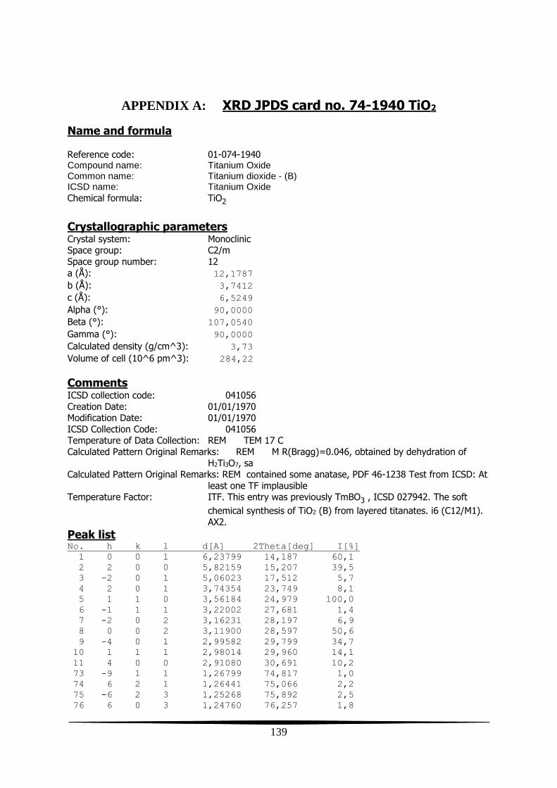
139
APPENDIX A: XRD JPDS card no. 74-1940 TiO2
Name and formula Reference code: 01-074-1940 Compound name: Titanium Oxide Common name: Titanium dioxide - (B) ICSD name: Titanium Oxide
Chemical formula: TiO2
Crystallographic parameters Crystal system: Monoclinic Space group: C2/m
Space group number: 12
a (Å): 12,1787
b (Å): 3,7412
c (Å): 6,5249
Alpha (°): 90,0000
Beta (°): 107,0540
Gamma (°): 90,0000
Calculated density (g/cm^3): 3,73
Volume of cell (10^6 pm^3): 284,22
Comments ICSD collection code: 041056
Creation Date: 01/01/1970 Modification Date: 01/01/1970
ICSD Collection Code: 041056 Temperature of Data Collection: REM TEM 17 C
Calculated Pattern Original Remarks: REM M R(Bragg)=0.046, obtained by dehydration of
H2Ti3O7, sa Calculated Pattern Original Remarks: REM contained some anatase, PDF 46-1238 Test from ICSD: At
least one TF implausible Temperature Factor: ITF. This entry was previously TmBO3 , ICSD 027942. The soft
chemical synthesis of TiO2 (B) from layered titanates. i6 (C12/M1).
AX2.
Peak list No. h k l d[A] 2Theta[deg] I[%]
1 0 0 1 6,23799 14,187 60,1
2 2 0 0 5,82159 15,207 39,5
3 -2 0 1 5,06023 17,512 5,7
4 2 0 1 3,74354 23,749 8,1
5 1 1 0 3,56184 24,979 100,0
6 -1 1 1 3,22002 27,681 1,4
7 -2 0 2 3,16231 28,197 6,9
8 0 0 2 3,11900 28,597 50,6
9 -4 0 1 2,99582 29,799 34,7
10 1 1 1 2,98014 29,960 14,1
11 4 0 0 2,91080 30,691 10,2
73 -9 1 1 1,26799 74,817 1,0
74 6 2 1 1,26441 75,066 2,2
75 -6 2 3 1,25268 75,892 2,5
76 6 0 3 1,24760 76,257 1,8

140
No. h k l d[A] 2Theta[deg] I[%]
77 3 1 4 1,24426 76,498 1,2
78 7 1 2 1,24154 76,696 6,3
79 1 3 0 1,23997 76,811 2,9
80 4 0 4 1,23239 77,371 0,2
81 -2 2 4 1,22918 77,611 0,6
82 -6 0 5 1,22559 77,881 0,4
83 -1 3 1 1,22265 78,104 0,4
84 -10 0 2 1,21363 78,797 1,0
85 -9 1 3 1,21037 79,050 0,9
86 -4 2 4 1,20756 79,271 4,3
87 -5 1 5 1,19783 80,044 0,6
88 8 0 2 1,19174 80,536 0,2
89 3 3 0 1,18728 80,901 0,8
90 -3 3 1 1,18605 81,003 1,0
91 -8 2 1 1,17935 81,560 0,4
92 -10 0 3 1,17309 82,089 0,4
93 -8 2 2 1,16881 82,454 2,5
94 -1 3 2 1,16432 82,842 1,0
95 6 2 2 1,15390 83,758 2,0
96 3 3 1 1,14758 84,325 0,6
97 1 1 5 1,14582 84,485 0,9
98 -3 3 2 1,14426 84,627 0,7
99 -6 2 4 1,14057 84,965 2,6
100 -9 1 4 1,12551 86,377 0,5
101 -8 0 5 1,12316 86,602 1,2
102 -8 2 3 1,12129 86,783 0,6
103 -5 3 1 1,10923 87,966 0,1
104 -10 0 4 1,10043 88,854 0,3
105 5 3 0 1,09860 89,041 0,2
106 7 1 3 1,09515 89,397 0,1
Stick Pattern

141
APPENDIX B: XRD JPDS card no. 28-0317 Nb2O5
Name and formula Reference code: 00-028-0317 Compound name: Niobium Oxide PDF index name: Niobium Oxide
Chemical formula: Nb2O5
Crystallographic parameters Crystal system: Hexagonal
Space group: P E
a (Å): 3,6070
b (Å): 3,6070
c (Å): 3,9250
Alpha (°): 90,0000
Beta (°): 90,0000
Gamma (°): 120,0000
Volume of cell (10^6 pm^3): 44,22
Comments Creation Date: 01/01/1970 Modification Date: 01/01/1970
Comment: Pattern at high pressure.
Peak list No. h k l d[A] 2Theta[deg] I[%]
1 0 0 1 3,93000 22,607 90,0
2 1 0 0 3,12000 28,587 100,0
3 1 0 1 2,44600 36,712 40,0
4 0 0 2 1,96200 46,234 30,0
5 1 1 0 1,80000 50,674 25,0
6 1 0 2 1,66300 55,187 30,0
7 1 1 1 1,63700 56,141 14,0
8 2 0 0 1,56500 58,971 12,0
Stick Pattern

142
APPENDIX C: PUBLISHED PAPER I

143
APPENDIX D: PUBLISHED PAPER II

144
APPENDIX E: PUBLISHED PAPER III