university of huddersfield repositoryeprints.hud.ac.uk/id/eprint/8797/1/hpmartinfinalthesis.pdf ·...
TRANSCRIPT

University of Huddersfield Repository
Martin, Haydn
Investigations into a multiplexed fibre interferometer for online, nanoscale, surface metrology
Original Citation
Martin, Haydn (2010) Investigations into a multiplexed fibre interferometer for online, nanoscale, surface metrology. Doctoral thesis, University of Huddersfield.
This version is available at http://eprints.hud.ac.uk/id/eprint/8797/
The University Repository is a digital collection of the research output of theUniversity, available on Open Access. Copyright and Moral Rights for the itemson this site are retained by the individual author and/or other copyright owners.Users may access full items free of charge; copies of full text items generallycan be reproduced, displayed or performed and given to third parties in anyformat or medium for personal research or study, educational or notforprofitpurposes without prior permission or charge, provided:
• The authors, title and full bibliographic details is credited in any copy;• A hyperlink and/or URL is included for the original metadata page; and• The content is not changed in any way.
For more information, including our policy and submission procedure, pleasecontact the Repository Team at: [email protected].
http://eprints.hud.ac.uk/

INVESTIGATIONS INTO A MULTIPLEXED FIBRE
INTERFEROMETER FOR ON-LINE, NANOSCALE,
SURFACE METROLOGY
HAYDN PAUL MARTIN
A thesis submitted to The University of Huddersfield in partial fulfilment of the requirements for the degree of Doctor of Philosophy
The University of Huddersfield in collaboration with Taylor Hobson Ltd.
April 2010

- 2 -
ABSTRACT
Current trends in technology are leading to a need for ever smaller and more complex featured surfaces. The techniques for manufacturing these surfaces are varied but are tied together by one limitation; the lack of useable, on-line metrology instrumentation. Current metrology methods require the removal of a workpiece for characterisation which leads to machining down-time, more intensive labour and generally presents a bottle neck for throughput.
In order to establish a new method for on-line metrology at the nanoscale investigation are made into the use of optical fibre interferometry to realise a compact probe that is robust to environmental disturbance. Wavelength tuning is combined with a dispersive element to provide a moveable optical stylus that sweeps the surface. The phase variation caused by the surface topography is then analysed using phase shifting interferometry.
A second interferometer is wavelength multiplexed into the optical circuit in order to track the inherent instability of the optical fibre. This is then countered using a closed loop control to servo the path lengths mechanically which additionally counters external vibration on the measurand. The overall stability is found to be limited by polarisation state evolution however.
A second method is then investigated and a rapid phase shifting technique is employed in conjunction with an electro-optic phase modulator to overcome the polarisation state evolution. Closed loop servo control is realised with no mechanical movement and a step height artefact is measured. The measurement result shows good correlation with a measurement taken with a commercial white light interferometer.

- 3 -
ACKNOWLEDGEMENTS
I would first like to thank my supervisor Jane Jiang for her guidance and belief in me
throughout this project. Her dedication to her students and work goes far beyond the
norm.
Secondly, thanks to all my colleagues in the Centre of Precision Technologies
including the director Liam Blunt. You have all made for a pleasant and enjoyable
place to work.
To those colleagues at Taylor Hobson, thank you for allowing me access to your
knowledge and expertise and also for your humour which helped to make my short
stay so enjoyable.
Thanks to Mum, Dad and Maria for getting me this far.
Finally, thank you to my partner Sarah without whose unbounded patience,
understanding and support I could never have completed this work.
This work is dedicated to the memory of my grandmothers, Muriel Martin and
Malvina Petravicius, both of whom sadly passed during its conception.

- 4 -
TABLE OF CONTENTS
1 Introduction ............................................................................................................................... 15 1.1 Overview ............................................................................................................................ 15 1.2 Measurement Process Types .............................................................................................. 16
1.2.1 In-process ...................................................................................................................... 16 1.2.2 On-line ........................................................................................................................... 16 1.2.3 Post-process ................................................................................................................... 16
1.3 Instrumentation for On-line Surface Metrology ................................................................. 16 1.4 Aim, Objectives and Contribution ...................................................................................... 17
1.4.1 Aim ................................................................................................................................ 17 1.4.2 Objectives ...................................................................................................................... 17 1.4.3 Contribution ................................................................................................................... 17
Thesis Structure ........................................................................................................................... 18 1.5 ..................................................................................................................................................... 18 1.6 Publications ........................................................................................................................ 19
2 Surface Metrology ..................................................................................................................... 21 2.1 Introduction ........................................................................................................................ 21 2.2 Surface Metrology .............................................................................................................. 21
2.2.1 Overview ....................................................................................................................... 21 2.2.2 Initial Development ....................................................................................................... 22 2.2.3 Characterisation ............................................................................................................. 22 2.2.4 Filtering ......................................................................................................................... 23 2.2.5 Parameterisation ............................................................................................................ 24 2.2.6 Areal Characterisation ................................................................................................... 26 2.2.7 Filtering for Areal Surface Characterisation .................................................................. 29 2.2.8 Freeform Surfaces ......................................................................................................... 29
2.3 Instrumentation for Surface Metrology .............................................................................. 30 2.3.1 Introduction ................................................................................................................... 30 2.3.2 Stylus Based Methods ................................................................................................... 30 2.3.3 Non-contact Methods .................................................................................................... 31 2.3.4 Summary ....................................................................................................................... 35
2.4 The Requirements for Online Measurement ...................................................................... 35 2.5 Conclusion.......................................................................................................................... 36
3 Light in Interferometers ............................................................................................................ 38 3.1 Introduction ........................................................................................................................ 38 3.2 Wave Propagation .............................................................................................................. 38
3.2.1 Scalar Optics .................................................................................................................. 38 3.2.2 Complex Amplitude ...................................................................................................... 39 3.2.3 Intensity ......................................................................................................................... 39 3.2.4 The Gaussian Beam ....................................................................................................... 40
3.3 Interference ........................................................................................................................ 43 3.4 Coherence ........................................................................................................................... 45
3.4.1 Phase Requirement for Observable Interference ........................................................... 45 3.4.2 The Superposition of Waves of Random Phase ............................................................. 45 3.4.3 Types of Coherence ....................................................................................................... 46 3.4.4 Temporal Coherence ..................................................................................................... 46

- 5 -
3.4.5 Wavetrains ..................................................................................................................... 48 3.4.6 Power Spectral Density and Linewidth ......................................................................... 49 3.4.7 Spatial Coherence .......................................................................................................... 50 3.4.8 Longitudinal Coherence ................................................................................................ 51 3.4.9 Interference of Partially Coherent Light ........................................................................ 51
3.5 Polarised Light ................................................................................................................... 53 3.5.1 The Polarised Nature of Light ....................................................................................... 53 3.5.2 The Poincaré Sphere Representation. ............................................................................ 54 3.5.3 Modelling polarisation state Evolution in Optical Fibre using Elliptical Retarders ...... 58
3.6 Fibre Optics ........................................................................................................................ 58 3.6.1 Historical Overview of Fibre Optics.............................................................................. 58 3.6.2 Structure of Optical Fibre .............................................................................................. 59 3.6.3 Operating Conditions ..................................................................................................... 60 3.6.4 Guided Modes ............................................................................................................... 62
3.7 Conclusion.......................................................................................................................... 64 4 Interferometry ............................................................................................................................ 65
4.1 Introduction ........................................................................................................................ 65 4.2 The Interferometer.............................................................................................................. 65
4.2.1 Background ................................................................................................................... 65 4.2.2 Fringes ........................................................................................................................... 66 4.2.3 Division Type ................................................................................................................ 67
4.3 The Michelson Interferometer ............................................................................................ 67 4.3.1 Apparatus....................................................................................................................... 67 4.3.2 Analysis ......................................................................................................................... 68
4.4 Interferometry for Surface Profiling ................................................................................... 71 4.4.1 Overview ....................................................................................................................... 71 4.4.2 Michelson ...................................................................................................................... 72 4.4.3 Mirau ............................................................................................................................. 73 4.4.4 Linnik ............................................................................................................................ 74 4.4.5 Limitations of Monochromatic Interferometry .............................................................. 74 4.4.6 Interrogating Interferometers ......................................................................................... 76
4.5 Optical Fibre Sensors ......................................................................................................... 76 4.5.1 Background ................................................................................................................... 76 4.5.2 Fibre Interferometers ..................................................................................................... 77 4.5.3 Advantages .................................................................................................................... 78 4.5.4 Issues ............................................................................................................................. 78
4.6 The Michelson Fibre Interferometer .................................................................................. 79 4.6.1 Apparatus....................................................................................................................... 79 4.6.2 The Directional Coupler ................................................................................................ 80 4.6.3 GRIN Collimators ......................................................................................................... 84 4.6.4 Mirrors ........................................................................................................................... 85 4.6.5 Detector ......................................................................................................................... 85 4.6.6 Laser Source .................................................................................................................. 87 4.6.7 Fibre Connections .......................................................................................................... 92
4.7 Phase Retrieval for Fibre Interferometers .......................................................................... 93 4.7.1 Nonlinear Phase-Intensity Relationship ........................................................................ 93 4.7.2 Operating Point Drift ..................................................................................................... 93 4.7.3 Passive Homodyne ........................................................................................................ 94 4.7.4 Heterodyne .................................................................................................................... 95 4.7.5 Synthetic Heterodyne .................................................................................................... 95 4.7.6 Active Phase Tracking Homodyne ................................................................................ 96 4.7.7 Phase Retrieval Issues Specific to Height Measurement ............................................... 97 4.7.8 Phase Shifting Interferometry ........................................................................................ 97

- 6 -
4.7.9 Phase Retrieval Methods for a Fibre Interferometer applied to Surface Measurement. 99 4.8 Conclusion.......................................................................................................................... 99
5 Initial Investigations into a Multiplexed Fibre Interferometer ............................................ 101 5.1 Introduction ...................................................................................................................... 101 5.2 Previous Work .................................................................................................................. 101
5.2.1 Description .................................................................................................................. 101 5.2.2 Limitations ................................................................................................................... 102 5.2.3 An Improved Method .................................................................................................. 103
5.3 Apparatus ......................................................................................................................... 105 5.3.1 Overview ..................................................................................................................... 105 5.3.2 Optical ......................................................................................................................... 105 5.3.3 Electronics ................................................................................................................... 107
5.4 Analysis of Instrument Performance ................................................................................ 108 5.4.1 Surface Height to Phase Relationship .......................................................................... 108 5.4.2 Optical Stylus by Wavelength Tuning ......................................................................... 109 5.4.3 Active Disturbance Rejection ...................................................................................... 113 5.4.4 Control Loop Analysis ................................................................................................ 123 5.4.5 Extraction of Phase Data ............................................................................................. 127
5.5 Implementation ................................................................................................................ 128 5.5.1 Practical Implementation of PI Control ....................................................................... 128 5.5.2 Closed Loop Control to Implement PSI ...................................................................... 129 5.5.3 Sequence of Operation ................................................................................................ 130
5.6 Experimental Results ........................................................................................................ 137 5.6.1 Introduction ................................................................................................................. 138 5.6.2 Reference Interferometer Disturbance Rejection ........................................................ 138 5.6.3 Measurement Interferometer Disturbance Rejection ................................................... 141 5.6.4 Absolute Displacement Accuracy ............................................................................... 143 5.6.5 First Step Height Measurement Result ........................................................................ 145 5.6.6 Second Step Height Measurement Result .................................................................... 147 5.6.7 Discussion ................................................................................................................... 149 5.6.8 Reference Interferometer Disturbance Rejection ........................................................ 149 5.6.9 Measurement Interferometer Disturbance Rejection ................................................... 149 5.6.10 Absolute Displacement Accuracy ........................................................................... 149 5.6.11 First Step Height ..................................................................................................... 150 5.6.12 Second Step Height ................................................................................................. 151
5.7 Conclusion........................................................................................................................ 151 6 Noise in Fibre Interferometers 153
6.1 Introduction ...................................................................................................................... 153 6.2 Noise Categories .............................................................................................................. 153
6.2.1 External Noise ............................................................................................................. 154 6.2.2 Intrinsic Noise ............................................................................................................. 154 6.2.3 Electronic Noise .......................................................................................................... 154 6.2.4 Optical Noise ............................................................................................................... 154 6.2.5 Mechanical Noise ........................................................................................................ 155 6.2.6 Summary ..................................................................................................................... 155
6.3 Polarisation Instability ...................................................................................................... 155 6.3.1 Modelling SOP Evolution in Optical Fibre using Elliptical Retarders ........................ 155 6.3.2 Fringe Visibility Dependence on SOP Evolution ........................................................ 157 6.3.3 Practical Observations of Polarisation Effects ............................................................. 160 6.3.4 Overcoming Polarisation Effects in Optical Fibre Interferometers ............................. 161
6.4 Discussion ........................................................................................................................ 165

- 7 -
6.5 Conclusion........................................................................................................................ 168 7 Rapid Phase Shifting Interferometer ..................................................................................... 170
7.1 Introduction ...................................................................................................................... 170 7.2 Rapid Phase Shifting Method ........................................................................................... 170
7.2.1 Overview ..................................................................................................................... 170 7.2.2 Electro-Optic Phase Modulator (EOPM) ..................................................................... 171 7.2.3 Bulk Electro-optic Phase Modulators .......................................................................... 173 7.2.4 Integrated Optics EOMs .............................................................................................. 173 7.2.5 Rapid Phase Shifting Method ...................................................................................... 175
7.3 Experimental Setup .......................................................................................................... 176 7.3.1 Apparatus..................................................................................................................... 177 7.3.2 Optical Probe ............................................................................................................... 178 7.3.3 Reference Arm ............................................................................................................ 179 7.3.4 Electronic Hardware .................................................................................................... 180 7.3.5 Software ...................................................................................................................... 184 7.3.6 General Points ............................................................................................................. 187 7.3.7 Balancing the Optical Paths ......................................................................................... 187 7.3.8 The Measurement Cycle .............................................................................................. 188 7.3.9 Rapid Phase Shifting Operation .................................................................................. 190
7.4 Control Loop Analysis ..................................................................................................... 192 7.4.1 Introduction ................................................................................................................. 192 7.4.2 Block Diagram ............................................................................................................ 192 7.4.3 z-domain Analysis ....................................................................................................... 193 7.4.4 Numerical Simulation .................................................................................................. 194
7.5 Experimental Results ........................................................................................................ 196 7.5.1 Introduction ................................................................................................................. 196 7.5.2 Stabilised Reference Interferometer ............................................................................ 196 7.5.3 Short Term Reference Interferometer Stability ........................................................... 197 7.5.4 SOP Variation in the Stabilised Measurement Interferometer..................................... 199 7.5.5 Reference Interferometer Stability Histogram ............................................................. 200 7.5.6 Stabilised Measurement Interferometer ....................................................................... 201 7.5.7 Step Height Measurement ........................................................................................... 202
7.6 Discussion ........................................................................................................................ 204 7.6.1 Stabilised Reference Interferometer ............................................................................ 204 7.6.2 Short Term Reference Interferometer Stability ........................................................... 204 7.6.3 SOP Variation in the Stabilised Measurement Interferometer..................................... 205 7.6.4 Reference Interferometer Stability Histogram ............................................................. 205 7.6.5 Stabilised Measurement Interferometer ....................................................................... 205 7.6.6 Step Height Measurement ........................................................................................... 206 7.6.7 General Points ............................................................................................................. 206
7.7 Conclusion........................................................................................................................ 207 8 Discussion and Conclusions .................................................................................................... 209
8.1 Introduction ...................................................................................................................... 209 8.2 Summary of Investigations ............................................................................................... 209
8.2.1 First Multiplexed Fibre Interferometer ........................................................................ 209 8.2.2 Second Multiplexed Fibre Interferometer with Rapid Phase Shifting. ........................ 210 8.2.3 Noise Sources and Magnitudes .................................................................................... 210
8.3 Discussion Points ............................................................................................................. 211 8.3.1 Instrument Comparison ............................................................................................... 211 8.3.2 Discrepancy between Stability Results ........................................................................ 211 8.3.3 Relative Probe Sizes .................................................................................................... 212 8.3.4 Measurement Period .................................................................................................... 213

- 8 -
8.3.5 Stability and Noise Performance ................................................................................. 213 8.4 Conclusion........................................................................................................................ 214
9 Further Work ........................................................................................................................... 217

- 9 -
LIST OF FIGURES
Figure 2.1 The S-parameter set (Jiang et al. 2007b) .............................................................................. 27 Figure 2.2 The V-parameter set (Jiang et al. 2007b) ............................................................................. 28 Figure 2.3 The feature parameter set (Jiang et al. 2007b) ..................................................................... 28 Figure 3.1 The superposition of two complex amplitudes in phasor form ............................................ 44 Figure 3.2 An arbitrary complex degree of coherence function ............................................................ 48 Figure 3.3 Example of Interference between two partially coherent waves .......................................... 53 Figure 3.4 The polarisation ellipse and its components ........................................................................ 55 Figure 3.5 A polarisation state p on the Poincaré sphere .................................................................... 56 Figure 3.6 Migration if the polarisation state from p to p′ as a result of action by a rotator ............ 57 Figure 3.7 Migration of the a polarisation state from point p to point p′ as a result of the action of
an elliptical retarder with a phase shift of ϕ and a fast axis orientation of ψ from the horizontal ..................................................................................................................................................... 58
Figure 3.8 Step index fibre structure ..................................................................................................... 60 Figure 3.9 Attenuation of optical fibre with wavelength (Dutton 1998, p.31) ...................................... 61 Figure 4.1 The Michelson interferometer .............................................................................................. 68 Figure 4.2 The Twyman-Green interferometer ..................................................................................... 69 Figure 4.3 The Michelson interferometric objective ............................................................................. 73 Figure 4.4 The Mirau interferometer objective ..................................................................................... 74 Figure 4.5 The Linnik interferometer objective .................................................................................... 74 Figure 4.6 A Michelson fibre interferometer ......................................................................................... 80 Figure 4.7 A 4 port directional coupler ................................................................................................. 81 Figure 4.8 Wavelength response of the PDDM981 photodiode (Wuhan Telecommunications)........... 87 Figure 4.9 A typical heterostructure laser diode for telecommunications (Bass & Stryland 2001) ...... 88 Figure 4.10 Ando AQ4320D Laser Cavity Schematic .......................................................................... 90 Figure 4.11 Hewlett-Packard HP8168F laser cavity schematic ............................................................ 91 Figure 5.1 Multiplexed fibre interferometer from Lin et. al. 2004 ...................................................... 102 Figure 5.2 Multiplexed Fibre Interferometer Schematic ..................................................................... 104 Figure 5.3 Optical probe schematic ..................................................................................................... 110 Figure 5.4 Angle sign definition for gratings ...................................................................................... 111 Figure 5.5 Linear dispersion vs. beam angle of incidence, α .............................................................. 112 Figure 5.6 Scan path linearity for various angles of incidence ............................................................ 112 Figure 5.7 Block diagram representation of the closed loop MFI ....................................................... 114 Figure 5.8 Equivalent representation of a PZT .................................................................................... 115 Figure 5.9 Simulated Bode plot and step response for a PZT ............................................................. 117 Figure 5.10 Simulated Bode-magnitude plot and step response for a transimpedance amplifier ........ 120 Figure 5.11 Block diagram representation of the closed loop MFI with the addition of an external
disturbance ................................................................................................................................. 121 Figure 5.12 Simulated Bode plot of the sensitivity function for varying integration gains ................. 123 Figure 5.13 For varying proportional gains ......................................................................................... 124 Figure 5.14 Simulated Nichols chart of the open loop response of the MFI for varying values of
integration gain. ......................................................................................................................... 126 Figure 5.15 Simulated closed loop response of the MFI to a setpoint change .................................... 127 Figure 5.16 Schematic of the optical probe with added PZT to apply disturbance to the measurand . 129 Figure 5.17 Functional diagram of the MFI ........................................................................................ 130 Figure 5.18 Event flow of MFI during the measurement cycle ........................................................... 131 Figure 5.19 Response of the interferometer with the required setpoints shown (angles are relative to
the quadrature point) .................................................................................................................. 133 Figure 5.20 Shift order of the setpoints during the measurement cycle .............................................. 134 Figure 5.21 Output of the tuneable laser analogue output during wavelength sweeping .................... 135 Figure 5.22 The effect of the active stabilisation for varying frequencies .......................................... 139 Figure 5.23 Actuating signal from PI controller for varying frequencies ............................................ 140 Figure 5.24 Attenuation of sinusoidal disturbance with increasing frequency .................................... 141

- 10 -
Figure 5.25 Simultaneous measurements of reference and measurement outputs over a 6 second period with active stabilisation on (upper) and off (lower) ................................................................... 142
Figure 5.26 Recorded displacements of measurement mirror by MFI and a linear fit of the results ... 143 Figure 5.27 Multiple measurements of a flat mirror............................................................................ 144 Figure 5.28 Multiple measurements of a flat mirror with DC offsets removed................................... 145 Figure 5.29 First step height artefact ................................................................................................... 146 Figure 5.30 Measurement result from MFI ......................................................................................... 146 Figure 5.31 Second step height artefact .............................................................................................. 147 Figure 5.32 Scanned step height with no disturbance ......................................................................... 148 Figure 5.33 Scanned step height with 750nm peak to peak induced disturbance ................................ 148 Figure 6.1 Poincaré sphere representation on an elliptical retarder and its effect on an SOP, p ....... 157 Figure 6.2 Poincaré sphere representation of the SOPs in an interferometers arms ............................ 158 Figure 6.3 Lumping two birefringences into one differential birefringence........................................ 158 Figure 6.4 Poincaré sphere representation of the input SOP and a differential birefringence ............. 159 Figure 6.5 Fringe visibility variance due to SOP evolution ................................................................ 160 Figure 6.6 Estimated worst case noise on MFI from quantifiable noise sources ................................. 167 Figure 6.7 Output noise histogram ...................................................................................................... 167 Figure 7.1 The rapid phase shifting concept ........................................................................................ 171 Figure 7.2 Operating principle of an electro-optic phase modulator ................................................... 173 Figure 7.3 Flow of events during rapid phase shifting ........................................................................ 175 Figure 7.4 Calibration of Vπ for an EOPM .......................................................................................... 176 Figure 7.5 Experimental Setup ............................................................................................................ 177 Figure 7.6 Optical probe scanning profile ........................................................................................... 179 Figure 7.7 Functional representation ................................................................................................... 180 Figure 7.8 Response of MFI to phase shifting ..................................................................................... 182 Figure 7.9 Response of EOPM voltage to an input square wave ........................................................ 182 Figure 7.10 DSP code function diagram ............................................................................................. 185 Figure 7.11 Diagram of Schwider-Hariharan phase shifting method .................................................. 186 Figure 7.12 Event flow during measurement cycle ............................................................................. 189 Figure 7.13 Laser move request timing diagram ................................................................................. 190 Figure 7.14 Oscilloscope trace showing rapid phase shifting with Carré algorithm ........................... 191 Figure 7.15 Oscilloscope trace showing rapid phase shifting with the Schwider-Hariharan algorithm
................................................................................................................................................... 191 Figure 7.16 Representation of control loop ......................................................................................... 193 Figure 7.17 Simulated closed loop step response ................................................................................ 194 Figure 7.18 Bode plot of sensitivity function ...................................................................................... 195 Figure 7.19 Drift seen in the stabilised/free running fibre interferometer ........................................... 197 Figure 7.20 Unstabilised reference interferometer with using the laser diode source1 ........................ 198 Figure 7.21 Stabilised output using Carré algorithm1 ......................................................................... 198 Figure 7.22 Stabilised output using Schwider-Hariharan .................................................................... 199 Figure 7.23 Drift of captured intensity values due to SOP variation ................................................... 200 Figure 7.24 Histogram of stabilized interferometer values ................................................................. 201 Figure 7.25 Histograms of stabilised measurement interferometer at various tunable laser wavelengths
................................................................................................................................................... 202 Figure 7.26 Step height sample measured using Taylor Hobson CCI ................................................. 203 Figure 7.27 Step sample profile as determined experimentally using a Taylor Hobson CCI .............. 203 Figure 7.28 Step Height as measured using the fibre interferometer .................................................. 204 Figure 9.1 Proposed idea for SLED based fibre interferometer. ......................................................... 218 Figure A.1 Photodiode equivalent circuit diagram .............................................................................. 235 Figure A.2 Transimpedance amplifier circuit diagram ........................................................................ 236 Figure A.3 Transimpedance amplifier represented with complex impedances ................................... 236 Figure A.4 LF356 transimpedance response ....................................................................................... 238 Figure A.5 Transimpedance amplifier noise model ............................................................................ 239 Figure A.6 Voltage and current noise simulation of LF356 and THS4062 transimpedance amplifiers
................................................................................................................................................... 244 Figure A.7 Frequency response for LF356 and THS4062 transimpedance amplifiers ....................... 244 Figure B.1 PI Controller Circuit Diagram ........................................................................................... 251 Figure B.2 LF356 based transimpedance amplifier circuit.................................................................. 252

- 11 -
Figure B.3 THS4062 based transimpedance amplifier circuit ............................................................. 252 Figure B.4 Interface Board Circuit Diagram ....................................................................................... 253 Figure B.5 Laser Diode Driver ............................................................................................................ 253 Figure B.6 Driver and Logic Level Translator Circuit Diagrams ........................................................ 254 Figure C.1 A Gaussian PDF ................................................................................................................ 257 Figure C.2 Spectral Densities of intrinsic fibre phase noise contributions .......................................... 275 Figure C.3 Effect of type 1 noise showing induced wraparounds ....................................................... 278 Figure C.4 Effect of type 1 noise ......................................................................................................... 279 Figure C.5 Histograms of type 1 input and output noise ..................................................................... 280 Figure C.6 Glitch induced by type 1 noise .......................................................................................... 280 Figure C.7 Effect of type 2 noise ......................................................................................................... 282 Figure C.8 Effect of type 3 noise ......................................................................................................... 283 Figure C.9 Effect of phase angle on type 2 and 3 noise ...................................................................... 284

- 12 -
LIST OF TABLES
Table 3.1 Gaussian beam parameters in relation to the Rayleigh range ................................................ 41 Table 3.2 FWHM spectral widths for common PSD profiles ................................................................ 50 Table 5.2 Rules for determining arctangent quadrant for the Carré algorithm .................................... 137 Table 6.1 Summary of noise sources and their magnitudes ................................................................ 166 Table 6.2 Effect of fringe visibility on output noise ............................................................................ 168 Table A.1 Parameter values for non-peaking response ....................................................................... 239 Table A.2 Simulated transimpedance amplifier noise magnitudes ...................................................... 245 Table C.1 Parameter values for Silica ................................................................................................. 274

- 13 -
LIST OF ABBREVIATIONS
AC Alternating Current ADC Analogue to Digital Converter AFM Atomic Force Microscope AM Amplitude Modulation APTH Active Phase Tracking Homodyne CCD Charge Coupled Device CCI Coherence Correlation Interferometer CLTF Closed Loop Transfer Function CMM Coordinate Measurement Machine CMOS Complementary Metal Oxide Semiconductor DAC Digital to Analogue Converter DAQ Data Acquisition DBR Distributed Bragg Reflector DC Direct Current DFB Gain Bandwidth Product DOF Depth Of Field GPIB General Purpose Interface Bus GPIO General Purpose Input Output GRIN Graded Index HWP Half Wave Plate IC Integrated Circuit IDE Integrated Development Environment IID Independently Identically Distributed IR Infrared ISO International Standards Organisation ISR Interrupt Service Routine JTAG Joint Test Action Group LAN Local Area Network LCP Left Circularly Polarised LED Light Emitting Diode LP Linearly Polarised LTI Linear Time Invariant LVDT Linear Variable Differential Transformer MEMS Micro-Electro-Mechanical System MEOMS Micro-Electro-Opto-Mechanical System MFD Mode Field Diameter MFI Multiplexed Fibre Interferometer MSPS Mega Samples Per Second N.A. Numerical Aperture NEP Noise Equivalent Power OCT Optical Coherence Tomography OLTF Open Loop Transfer Function OPD Optical Path Difference PC Personal Computer PCB Printed Circuit Board PDF Probability Density Function PGI Phase Grating Interferometer PI Proportional Integral PID Proportional Integral Differential PM Polarisation Maintaining PSD Power Spectral Density PSI Phase Shifting Interferometry PZT Piezo-electric Transducer QWP Quarter Wave Plate RAM Random Access Memory

- 14 -
RCP Right Circularly Polarised RIN Relative Intensity Noise RMS Root Mean Square RPS Rapid Phase Shifting SLED Super-luminescent Light Emitting Diode SM Single Mode SNR Signal to Noise Ratio SOP State Of Polarisation SPI Serial Peripheral Interface STM Scanning Tunnelling Microscope TE Transverse Electric TEM Transverse Electromagnetic TIR Total Internal Reflection TM Transverse Magnetic TTL Transistor-Transistor Logic VI Virtual Instrument VSWLI Vertical Scanning White Light Interferometry WDM Wavelength Division Multiplexing WLSI White Light Scanning Interferometer

- 15 -
1 Introduction
1.1 Overview
High precision manufacture covers a variety of tools and techniques for producing
both the structured and stochastic surfaces that are becoming more and more
prevalent in today’s technologies. While manufacturing technologies have advanced
in their ability to produce high-precision surfaces, the metrology needed for their
characterisation has progressed at a slower rate. Certainly, a level of maturity has
been reached in one sense; instrumentation with the ability to measure surfaces on the
sub-nanoscale and upwards is available and well established.
The specific techniques used to carry out metrology are dependent upon the
application with contact based methods using styli providing the largest potential
range to resolution ratio. Non-contact methods are preferred when surface
characteristics are such that contact methods would be destructive. Although various
optical approaches have been developed it is interferometry that has seen the greatest
success, mainly due to its high vertical resolution, traceability and areal capture
ability. This has been initially through the development of phase shifting
interferometry, which became a powerful tool with the advent of cheap computer
processing and CCD arrays. After this the development of vertical scanning white
light interferometry (VSWLI) further extended capabilities in terms of range. In
addition, its ability to acquire fast areal data makes it an attractive proposition for the
types of surface to which it is suited.
Both optical and stylus based instruments suffer from a number of limitations. They
tend to be large in size and heavy in order to provide the environmental stability
required for reliable sub-nanometre resolution measurement. During a manufacturing
process, it is necessary to be able to characterise the workpiece to ensure it meets
specification. Current high precision metrology instrumentation has a major
disadvantage in this sense, it generally requires the removal of the workpiece for
characterisation. While this is clearly time and labour intensive, resulting in a drop in
throughput, it is also often very problematic due to the difficulty of precisely
realigning the machine tool and/or workpiece. In general, a method for measuring the
- 16 -
process with the workpiece holds great advantage in terms of labour and
manufacturing throughput.
1.2 Measurement Process Types
Vacharanukul and Mekid (2005) neatly divide the act of measurement during the
manufacturing process in three ways; in-process, on-line and post-process.
1.2.1 In-process
In-process measurement is the act of measuring the workpiece during the process of
manufacture, that is while the machining actually takes place. This is generally the
most challenging area for measurement in that any metrology technique must deal
with added difficulties of vibration and the presence of lubricants or debris.
1.2.2 On-line
On-line (alternatively on-machine or in-situ) measurement is that which takes place
without the removal of a workpiece from the machine tool. Unlike in-process
measurement however, the manufacturing is actually halted during the measurement
period. This relaxes significantly some of the challenges for implementation while
also providing the advantages associated with not having to remove/refit the
workpiece.
1.2.3 Post-process
Post-process measurement is the standard method for inspection in high precision
manufacturing. It requires the physical removal of the workpiece after which the
measurement takes place on a separate, dedicated instrument. Not only does the
measurement normally require time consuming and skilful alignment procedures, any
further alteration to be made in light of the results require the re-alignment of the
workpiece on the machine tool. Typically measurement is not automated and as such
throughput tends to be decreased substantially.
1.3 Instrumentation for On-line Surface Metrology
There are specific requirements for metrology instrumentation that is more suited for
integration or retrofit into manufacturing technology in order to provide an on-line

- 17 -
surface metrology role. Such devices would require a small, compact probe that could
be flexibly mounted close to the machine tool/workpiece without fouling any of the
workings. Non-contact measurement would also be advantageous in this situation as
the probe could be placed away from the surface to some degree. While in general the
machining used for high precision manufacture is by necessity well stabilised against
environmental disturbance, any retrofit device will not necessarily be within the
physical metrology frame, hence some robustness against temperature drift and
stability would be beneficial.
Optical fibres, with their ability to move light into places very easily, provide
interesting prospects for application to online surface metrology. The concept of a
small optical probe, mounting at the head of a fibre is an attractive one from the point
of view installing onto a machine tool. With such a device, the interrogation optics
and associated electronics could be placed separately and conveniently, away from
the probe head.
1.4 Aim, Objectives and Contribution
1.4.1 Aim
To investigate the potential for applying optical fibre interferometry in on-line
nanoscale surface measurement applications.
1.4.2 Objectives
• To develop a fibre optic interferometer capable of measuring nanoscale
surface texture.
• Present a small, compact and remote mountable probe head.
• Feature an optical stylus utilising wavelength scanning and a dispersive
element to provide fast profile measurement without mechanical movement.
• Be robust against environmental perturbation.
1.4.3 Contribution
The work contained in this thesis has made the following novel contributions:

- 18 -
• Development and demonstration of a rapid phase shifting technique, using an
integrated optic electro-optic modulator, to obtain real-time phase information
from a fibre interferometer which is insensitive to polarisation state evolution.
• Development and demonstration of active vibration compensation using real-
time calculated phase feedback to stabilise the all-fibre interferometer path
length by the use of a separate reference wavelength.
• Demonstration of a stabilised multiplexed fibre interferometer to resolve a
step height of several hundred nanometres using a compact, remote
mountable fibre probe.
1.5 Thesis Structure
This study relates work done on the development of a fibre optic interferometer for
use in surface measurement applications, with the aim of producing an instrument
capable of producing robust nanoscale measurement in a compact form.
This study comprises a number of components to fulfil the overall aim:
• Chapter 2 presents a brief description of the development of surface
metrology and provides introduction to some of the terminology used in the
field. There is also an appraisal of current metrology capabilities and
instrumentation and a consideration of their application to online
measurement.
• Chapter 3 introduces some basic concepts and terminology describing the
nature of light. The chapter concentrates on those areas relating to
interferometry and fibre-optics.
• Chapter 4 gives an overview of interferometry for surface metrology and
describes established techniques and methodologies. By the end of the
chapter, the methodologies suitable for implementing a fibre interferometer
sensor for surface metrology are identified.
• Chapter 5 describes initial investigations into the use of a fibre interferometer
for surface measurement in order to determine the feasibility of such an

- 19 -
approach. The operation of the instrument is confirmed and its performance
with regard to measurement stability evaluated.
• Chapter 6 identifies the main theoretical noise sources present in fibre
interferometers and associated electronic subsystems. Noise sources are
grouped by type and an analysis of each type’s effects is performed. A
theoretical noise floor is presented and the likely main noise sources (and
their magnitudes) are identified.
• Chapter 7 investigates a second fibre interferometer apparatus with a different
design to attempt to overcome some of the limitations in the first instrument.
Here a novel methodology of rapid phase shifting is implemented in order to
improve performance. In addition the all-fibre design allows for the
realisation of a much more compact probe.
• Chapter 8 presents an appraisal of the investigated apparatus and implemented
methodologies.
• Chapter 9 considers some potential avenues for further investigation and
improvement.
The results of the first investigation into a fibre interferometer design (see chapter 5)
highlighted many of the weaknesses and difficulties with using fibre interferometers
for surface metrology. This included the problem of polarisation state evolution in the
fibre, which resulted in low frequency drift when using closed loop feedback. In
addition the physical size of the optical probe was such that it was not very suitable
for online mounting. These issues were taken into consideration and a new optical
design and alternative interrogation method was developed and investigated in
chapter 7.
Proof of concept for the idea was obtained through this second investigation. The
theoretical noise study suggests with some additional engineering, a viable surface
metrology instrument may be developed using the proposed methodology.
1.6 Publications

- 20 -
The work in this thesis has produced three peer reviewed journal papers, one
international patent and 3 conference papers. A full publication list may be found in
the Publications and Awards section at the end of this thesis.

- 21 -
2 Surface Metrology
2.1 Introduction
This chapter introduces surface metrology and gives a brief overview of its
development. Concepts are introduced in a rough historical context in order to make
clear the way the science has developed. Terminology used within the field is
introduced and explained.
The wide range of instrumentation used for the retrieval of surface topographic
information is described. Reference is also given to the physical location and the
point in time during the process at which the metrology takes place within the
manufacturing cycle. Finally, a description of metrology needs for the future with
regard to online methods is made.
2.2 Surface Metrology
2.2.1 Overview
Jiang et al. (2007a) give the definition of surface metrology as, ‘the science of
measuring small-scale geometrical features on surfaces: the topography of the
surface.’
The measurement of surfaces comprises two essential elements; the physical retrieval
of surface topography information by instrumentation, and the subsequent analysis of
that information (characterisation). Surface metrology is a relatively recent scientific
field and has historically been driven by technological developments in other fields.
For instrumentation this has been through the development of sensors, optics and
digitisation techniques. Characterisation has been driven by advances in computing
and the application of mathematical techniques such as digital filtering, wavelet
theory and region detection.
As the need for more and more precise engineering has evolved, the enabling
technologies and techniques for surface metrology have also done so. So too has the
understanding of the importance of surface characteristics on the function of a surface
in a given application.

- 22 -
2.2.2 Initial Development
At the turn of the 19th century the measurement of surface texture was confined to the
subjective inspection by eye (with or without a microscope) or the running of a
fingernail across a machined surface. In this way a skilled operator could gauge the
approximate roughness of the surface to some degree. The main concern was in the
height of the surface roughness normal to the surface as this had an understood effect
on assembly tolerances. Also of interest was the geometry of the roughness because
of its impact in contact applications. It was not until 1919 that the first instrument
was designed by Tomlinson at National Physical Laboratory (NPL) to specifically
measure the height of the surface roughness. The real development of instrumentation
however did not really begin until the 1930s when stylus based methods became
quickly established through the work of several companies worldwide. These
instruments allowed the recording of a profile of the surface topography along one
lateral axis.
2.2.3 Characterisation
With the advent of instrumentation to provide a profile of surface topography there
was another issue to be considered; what to do with the profile data. There were two
polarised viewpoints on how to characterise a surface; to use a simple number on a
scale (which relates to some definable surface attribute), or to use the complete
profile. Neither of these methods where very suitable for linking surface texture with
function; one is too simple, the other overly complex. The first step toward modern
characterisation of surface texture was given by Abbott and Firestone (1933) whose
material to air ratio curve provided a means of linking function (for the case of
contact) with simple numerical parameters. Such was the success of the method that
it is still in use today in assessing the manufacture of bearing and sealing surfaces.
As surface metrology matured as a discipline throughout the 1940s and 50s it became
apparent that the spatial frequencies contained in a surface profile could be usefully
separated into three ranges, named roughness, waviness and form. The definitions of
these ranges result from their origin in the manufacturing process (Whitehouse 2002,
ch. 1).

- 23 -
• Roughness is the texture imparted due to the machining process. It is
inevitable and unavoidable result of the manufacturing process.
• Waviness is the result of problems in the machine tool, possibly a lack of
stiffness or some form of harmonic disturbance. It is often periodic in nature
and occurs at longer wavelengths than the underlying roughness. It may also
occur as a slow moving random type wave.
• Form is the underlying surface geometry and comprises the longest
wavelengths of the surface. Form errors may be introduced by into the surface
geometry by longer term effects such as thermal changes.
So these three terms result from the manufacturing process, machine tool and design
respectively. Once this had been established the potential uses were obvious, analysis
of waviness for instance could yield information about machine tool problems such
as excess chatter. The separation and characterisation of the surface roughness
allowed a direct assessment of the manufacturing process.
2.2.4 Filtering
Throughout the 1950s the problem of effectively separating roughness from waviness
was considered. Mechanical and electrical methods were both investigated but by
1963, the way forward was clear. Electronic filtering could simply and easily
simulate the filtering of the real profile and acted directly upon the analogue output
produced by stylus instruments. Initially the filtering was provided by a simple
cascaded 2RC filter but further improvements soon came along in the form of phase
corrected filters, although these were difficult to implement in analogue electronics.
The advent of computers and digital techniques in the late 60s provided the next great
leap forward, allowing the accurate modelling of filters in software and enabling
more complex analysis. Digital storage meant the chart recorder had seen its day and
data could now be analysed at leisure using a multitude of different filters. Digital
storage and analysis meant that characterisation was for the first time separable from
the instrumentation.
The actual definitions (and the cut off wavelengths) for roughness, waviness and
form are extremely dependent on the surface being characterised. However roughness

- 24 -
is ultimately bounded at its upper frequency by the stylus tip size (or resolving power
in optical applications). Form is bounded by the size of the workpiece. The frequency
breakpoints that bind waviness are rather more ambiguous however; a watch spindle
a few millimetres in length and an axle in a motor vehicle will have substantially
different cut-offs frequencies.
Generally a sampling length over which a parameter is to be computed must be
defined. The sampling length chosen is dependent on the process being examined; the
values differ between periodic and non-periodic profiles for instance. A suitable
sampling length is iteratively arrived at from an initial estimation of a parameter
combined with several measurements at different sample lengths (Whitehouse 2002,
ch.2).
For the case of profile measurements, three cut-off wavelengths are defined for use
extracting roughness and waviness profiles:
λs is the short cut-off wavelength for the roughness profile. This is to separate the low
pass filtering of the stylus from the roughness profile. This is important to ensure that
any stylus wear or damage does not alter the roughness profile.
λc defines the cut-off wavelength separating the roughness and waviness profiles.
λf is the longest cut-off wavelength and separates the waviness profile and the form
of the workpiece.
The usual filter type used to extract the roughness and waviness profiles is the
Gaussian filter, chosen because it is easily generated digitally, phase corrected and
symmetrical. The cut-off wavelengths are defined as being at the 50 % amplitude
transmission points of the filter characteristic.
There are occasions when it is not strictly necessary to separate waviness and
roughness when trying to evaluate the surface function.
2.2.5 Parameterisation
The link between a surface function and its topography is one of the key reasons for
carrying out measurements on surfaces. Another is to enable the control of the
manufacturing process and to isolate issues in materials, tooling and the
manufacturing environment. Having suitably filtered a profile the obvious question is

- 25 -
what to do with the data. In some way it is necessary to link the data to a functional
prediction or process control. The aim of parameterising the data is to provide tools
for making that link. Early instrumentation yielded only simple parameters such as Ra
which is the average height deviation of roughness from the mean line. These simple
parameters came about because they could easily be ascertained from the chart
readouts produced by early instrumentation. The advent of computers and digital
storage allowed for the expansion of the number of available parameters as well as
the complexity of those parameters. One upshot of all this was the so-called
‘parameter rash’ (Whitehouse 1982) as researchers were now able to develop
parameters at will. The result was a large number of parameters having significant
redundancy and overlap.
Profile parameters fall into four base categories: amplitude, spatial, hybrid and
statistical.
Amplitude parameters are those which consider only the height variation of surface
roughness. Examples include:
• Rq the root mean square (RMS) deviation of height from the mean line
• Rz the height difference between the five highest peaks and the five lowest
valleys
Spatial parameters are those that consider the spacing of surface features. They
include the average distance between mean line crossing and the average peak
density. Generally spatial parameters are found most useful in conjunction with
amplitude parameters in the form of a hybrid parameter.
Hybrid parameters incorporate amplitude and spacing information. Examples
include:
• Δq is the RMS slope of the profile.
• ρ is the average curvature of the profile.
Historically, these parameters proved difficult to access because of the difficulty
obtaining the reliable differentials required using analogue electronics. Even with
digital methods the act of differentiation conspires to amplify noise on the result and
as such care must be taken.

- 26 -
Statistical parameters often appear in the form of curves such as material ratio
(Abbott-Firestone curve), autocorrelation and amplitude distribution which are
generally of use for random process analysis. They essentially remove positional
dependence, thus suppressing any localised random effects. This means that such
curves tend to be more stable across a surface and can reveal underlying information
that may be not be apparent when using other parameters. The power spectrum can
also reveal underlying harmonic information produced by tool feed in, for instance,
turned surfaces.
This brief overview is intended only to give a feel for parameter use and derivation in
surface metrology. Whitehouse (2002) gives a detailed description of parameters in
his exhaustive work on the subject of surface metrology.
2.2.6 Areal Characterisation
Historically, profile measurement has always been the main tool in surface analysis.
However surfaces, and their interactions, are by nature areal (3D). As such better
functional determination might be anticipated if a surface is analysed in this way.
The term ‘areal’ is used in surface metrology to make a clear distinction from true 3D
measurement methods, as carried out by devices such as coordinate measurement
machines (CMM). Most surface metrology instrumentation takes a plan view of a
surface and presents height data over an area. The measurement of sidewalls, for
instance, is not possible so the information obtained is 2½D, or areal.
In recent times, areal surface analysis and characterisation has become more
widespread. This major change in approach to surface measurement and
characterisation rode upon the increasing availability of computing power in the
1980s. Areal measurement was first investigated in the late 1960s in the form of
stylus instruments with a translation stage for stepping the workpiece in the second
lateral dimension. However it was increasing computing power that allowed the
processing of the vast increase in data taken from such instruments that made areal
characterisation feasible. Commercial stylus instruments for areal surface
measurement were becoming available in the early 1990s. The development of other
instrumentation such as scanning white light interferometers (SWLI), phase shifting

- 27 -
interferometers and atomic force microscopes (AFM) also pushed forward areal
measurement.
The gradual shift to areal measurement has required some conceptual changes in
surface characterisation. The development of 14 parameters for the quantifying of
areal surface texture was initially made by Stout et al. (1994a and 1994b). These so
called ‘Birmingham 14’ parameters were somewhat theoretical and in some instances
ill defined mathematically, especially in regard to defining hills, valleys and how they
interconnect. They did however supply a solid basis from which to derive a more
rigorous and practical parameter set. The European Surfstand project (E.C. Contract
No SMT4-CT98-22561, 1998) produced this more rigorous set of parameters which
is made up of field and feature parameters.
The field parameters consist of 12 S-parameters and 13 V-parameters. The S-
parameters are ‘surface’ parameters and are made up of amplitude, spacing, hybrid,
fractal and other parameters.
Figure 2.1 The S-parameter set (Jiang et al. 2007b)
V-parameters are ‘volume’ parameters and are made up of linear areal material ratio
curve, void volume and material volume parameters (Blunt & Jiang, 2003).

- 28 -
Figure 2.2 The V-parameter set (Jiang et al. 2007b)
S-parameters require the exact location of valleys and peaks and this is provided by
the use of feature extraction by Wolf pruning in avoiding false peaks/pits due to noise
(Scott 2003). This feature extraction method has been used to provide the
segmentation of surface topographic features and derive a set of 9 feature parameters
(Scott 2009). These features parameters are anticipated to be become very important
in the analysis of deterministic (as opposed to stochastic) surfaces that are becoming
more and more economically important. A deterministic surface is one that has a
definable pattern. Examples are tessellated surfaces (e.g. road signs, golf balls),
Fresnel lenses and diffraction gratings.
Figure 2.3 The feature parameter set (Jiang et al. 2007b)

- 29 -
At the time of writing the new areal surface texture parameters are in the process of
being committed to the international standard ISO 25178 series.
2.2.7 Filtering for Areal Surface Characterisation
Advancements in filtering have been concurrent with the development of areal
surface parameters. The standard filter for separating roughness, waviness and form
from the primary profile was a Gaussian filter in 2D analysis. However the
application of new mathematical techniques, in particular wavelet decomposition, has
refined the separation of scales in addition to being faster (Jiang & Blunt, 2004).
Other filters that have been investigated and authorised for ISO standard use are
spline, robust Gaussian and morphological filters.
Because of the expansion of filtering methods for areal surfaces the vernacular for
describing filtering has also been consciously altered. The terminology of roughness
and waviness has been superseded by the concept of scale limited surfaces. The areal
surface is scale limited by the application of some combination of an S-filter, L-filter
and F-operator. The F-operator is defined as an operator because both form fitting
and removal is performed. The S/L-filters and F-operators are now defined by a
nesting index, which is equivalent to the filter cut-off for linear filters, but extends
generality to allow for the parameter definition for other filtering methods such as
wavelet transforms.
2.2.8 Freeform Surfaces
Manufacturing technology has begun to move away from simple geometries for
surfaces and is now capable of producing surfaces with more complex geometries.
One prime example is in optics manufacture where freeform geometries can produce
smaller optics with less glass and improved performance. The scope of freeform
optics is wide and the potential production quantities large; mobile phone cameras,
laser printers, biomedical and telecommunications are some example applications of
freeform optics.
Freeform surfaces have no axes of rotation and present a major problem for
characterisation due to the difficulty of fitting the form. Work is ongoing in

- 30 -
developing optimised fitting algorithms to provide more accurate and consistent
surface fitting (Jiang et al., 2007b).
2.3 Instrumentation for Surface Metrology
2.3.1 Introduction
When grouping surface metrology methods it is useful to consider two factors; the
method employed and the location relative to the manufacturing process at which it is
carried out.
The usual way is to group measurement methods into two basic camps; the contact
based methods (using a stylus of some description) and the non-contact methods.
2.3.2 Stylus Based Methods
The stylus method was the original method of profiling a surface and is still very
prevalent today. The resulting profile obtained is a convolution of the geometry of the
stylus tip and the surface. As such the shape and size of the stylus tip is an important
parameter. Stylus based methods often use inductive type sensors such as linear
variable displacement transformer (LVDT) which are coupled to the vertical
movement of the stylus. For more accurate work optical methods are employed to
gauge the stylus deviation, the Taylor Hobson PGI range being an important example
of such a method which delivers a large vertical range and high resolution.
The stylus method is limited inherently by the fact it makes contact with the surfaces,
the resulting pressures generated by the stylus as it traverses the surface can damage
it if it is soft. Conversely, the stylus can be worn down by particularly abrasive
surfaces resulting in inconsistency of measured data for any given measurement run.
Song & Vorburger (1991) give a good overview of the stylus method emphasising
the importance of low stylus force and a small tip size. Several methods have been
investigated to lower the stylus force, Weckenmann et al. (2006) reviews several
methods with reference to contact probing for micro-electrical mechanical systems
(MEMS). Low force optical fibre based contact probes have been devised which
provide good access to high aspect ratio features and very low contact force, one
example is given by Muralikrishnan et al. (2006). Another technique is the servo-
driven stylus, where a piezoelectric transducer is used to actively maintain a constant
- 31 -
stylus force. This has the advantage of reducing stylus force as well as allowing faster
measurement without skipping (Bauza et al., 2006).
Another major disadvantage of contact methods are their slowness, this being
especially the case when multiple passes of a stylus must be made over a surface in
order to create a full 3D (or areal) topography of the surface. Speed is limited by the
mechanical motion required and the need to prevent the stylus skipping, this being a
problem that increases with the reduction of applied stylus force.
Another set of methods that falls uncomfortably into the stylus bracket are those of
scanning tunnelling microscopy (STM) and atomic force microscopy (AFM). While a
stylus is present, it is not a pre-requisite that it actually makes contact with the
surface. The STM method monitors the tunnelling current flowing between a minute
stylus tip and a conductive surface. By either monitoring the current variation or
adjusting the tip height to keep it constant, the surface topography may be obtained.
The AFM method relies on the deflection of a cantilever by atomic forces at the
surface; the tip need not be in physical contact with the surface, although it may be in
some modes of operation. The deflection of the cantilever is usually assessed by laser
beam deflection or interferometry. Both techniques can provide exceptionally high
lateral resolutions due to extremely small tip dimensions, enabling measurements to
be made down to the atomic and molecular scales. Using these devices however is in
general complex and time consuming; in addition, the equipment is expensive
(Whitehouse, 1997). The lateral range is usually very limited, only a few tens of
microns, although there is ongoing work to increase this (Mazzeo et al., 2009).
2.3.3 Non-contact Methods
It is possible to separate non-contact methods into two main camps; those utilising
optics and those that apply some other technique.
Non-optical methods include capacitive, inductive (eddy-current), ultrasonic and
pneumatic. In general it is found that these methods do not provide the lateral
resolution required for surface roughness at the micro and nano-scales. Generally
these methods are resigned to larger macro-scale consideration. In the case of
inductive techniques they are also very material dependent.

- 32 -
Optical methods are inherently much faster than the stylus methods and have obvious
advantages in their non-contact nature for delicate samples. In areal measurements
they really come into their own over stylus techniques with regard to acquisition
speed; this may also have knock on benefits for the measurement stability.
They do require a certain amount of reflectivity in the surface which can lead to
problems for the measurement of specular surfaces with steep gradients (high aspect
ratios) as more light is reflected away from the probe. Another issue is that the optical
surface is not the same as the tactile surface and the differences become more
prevalent at nanometric measurement levels. One example of the difference has been
highlighted by Rhee et al. (2005) and relates to the discrepancy between roughness
results obtained with a stylus method and a vertical scanning white light
interferometer (VWLSI).
Vorburger and Teague (1981) give a good summary of optical techniques for the
evaluation of surface topography. Optical devices may be divided into profiling and
parametric methods. Profiling is where the topology is derived point by point and the
parameters then deduced from the raw data. Of course stylus based methods are also
profiling, and one may also consider full-field interferometric measurement a
profiling technique even though it captures a whole area at once.
Parametric
Parametric methods are those techniques which derive a given surface parameter
such as the Rq directly. Such methods analyse the properties of light reflecting off a
rough surface. Some examine the total intensities of either the diffuse or specular
radiation. With increasing Rq the diffuse radiance increases, while at the same time,
the specular component decreases. Others measure the diffuseness or the actual
angular distribution of the reflected radiation. All these scattering methods rely
heavily on empirical data and curve fitting since deriving the results from optical
theory is intractable for a surface of any complexity.
Other parametric methods to have been investigated include diffractometry,
ellipsometry and speckle interferometry. The diffractometer is interesting in that it
produces a real-time power spectral density of the surface for smooth surfaces (Rq <

- 33 -
λ/6). It is quite insensitive to position and surface speed and is thus a good candidate
for fitting in-process.
Ellipsometry is a technique well associated with the measurement of the refractive
index of solids and films, as well as thickness in the case of the latter. Ellipsometry
considers the change of the polarisation state of light being reflected from the surface.
Unfortunately the change in polarisation may be imparted by many factors besides
the surface topography including material composition, temperature and strain.
Generally no monotonic relationship between surface roughness and any
ellipsometric parameter has been convincingly found (Whitehouse 2002, ch. 8).
Speckle interferometry has been a fruitful path for the investigation of surface
roughness. It relies on the examination of the localised intensity variation (speckle)
created by the scattering of coherent light. Either the Fraunhofer or Fresnel patterns
can be investigated; the names being analogous to the observation of diffraction
phenomena. There are two basic types of observation that are made; speckle contrast
and speckle pattern decorrelation.
Speckle contrast measurements are performed by detecting the variation in intensity
of a speckle field as the surface (or detector) moves. This is done by ensuring the
aperture of the detector is smaller than the speckle grain size. This method has clear
benefits for on-line manufacturing as it requires the movement of the surface to
operate. A good linearity is found for speckle contrast and roughness for Rq values
less than the coherence length (or spatial coherence) of light source used. Speckle
contrast with a short-coherence source was first investigated by Sprague (1972) as a
way to increase the operating range. The speckle contrast was found to increase
monotonically (though not linearly) with the Rq value of the surface. More recent
work such as that by Lehmann et al. (1997) has involved more complex analysis of
speckle grain shape.
In speckle correlation, separate speckle patterns are obtained by either altering
wavelength or the angle of incidence of the source light. The cross correlation
between the obtained speckle patterns can be related to the Rq results obtained from a
stylus instrument. This method can determine Rq values of much larger than the
wavelength of the illuminating light; this is its main advantage over speckle contrast
(Dhanasekar et al. 2008).

- 34 -
The limitations of speckle interferometry lie in assumptions that the surface height
distribution is Gaussian and only a single scattering takes place in the theoretical
evaluations. In reality, there are usually deviations in experimental results because of
these assumptions.
In general light scattering methods are attractive for on-line measurement of surface
roughness parameters. This is because of their insensitivity to alignment and
vibration. Unfortunately light scattering methods require a theoretical model of a
surface in order to gauge roughness and as such they often fall down practically
especially when applied over a range of sample types. Moreover, the information
they provide is too limited, only an area averaged parameter is obtained. A true
profile of the surface heights is not obtainable so it is not possible to examine
structured surfaces, provide graphical information or perform any complex analysis.
Profiling
Non-contact profiling may be grouped as interferometric and non-interferometric.
Interferometric devices are many and varied and this thesis will deal with a few of the
major variants of such devices in more detail in chapters 3 and 4. Suffice to say that
that in recent times it is the vertical scanning white light interferometer that has
proved the most fruitful commercially, providing sub-nanometre resolution over
several hundred microns of range (Taylor Hobson 2009a, Veeco 2009) with capture
times taking several tens of seconds for a full-field. Other interferometric methods
such as shearing interferometry and phase shifting interferometry see more specific
use in the field of surface metrology, particularly in optics manufacture.
Non-interferometric options for profiling are fairly restricted. There are some
methods based on confocal and beam scanning (or flying spot) microscopy. One
example is the focus detection follower first suggested by Depuy (1967). Here the
objective lens is servoed to keep the object image in focus above the surface; the
control signal from the servo then relates to the surface height profile. Zhang and
Lilong (1997) expanded upon this technique by measuring the servoed displacement
with an interferometer.
Another method is the chromatic aberration surface profiler first suggested by
Molesini and Quercioli (1986). Here an objective lens, purposefully produced with

- 35 -
large longitudinal chromatic aberration, is used with a white light source to generate a
set of focal points which have a distance to wavelength dependence. The reflected
light from the surface is inspected by a spectrometer, the wavelength of the intensity
peak then relates to a known focal distance. This method has seen some commercial
success as it is relatively fast.
An interesting technique has been investigated by Taguchi et al. (2003) in which the
power spectrum of a surface is derived from the Fraunhofer diffraction intensity.
Using this and the object intensity from the surface the phase is retrieved and the
surface reconstructed. While this method is fast, it is currently restricted to those
surfaces having a specific and periodic structure.
2.3.4 Summary
A large array of available surface measurement techniques have been examined in
this section. They have been assessed for their suitability for implementation for on-
line surface measurement. Contact (stylus) based methods are found to be too slow
and cumbersome. Non-contact, parametric methods such as light scattering are not
information rich enough, providing only an averaged area value for surface
roughness. Non-contact profiling methods such as white light interferometry are able
to provide the full profile information required but are generally too bulky implement
on-line.
2.4 The Requirements for Online Measurement
The work in this thesis aims at making progress in the direction of producing a viable
on-line surface measurement at the micro and nanoscale. Modern manufacturing
techniques such as lithography and fast tool servo diamond turning are enabling the
productions of complex surface micro-features for applications such as MEMS,
MEOMS (Micro Electro-Optical-Mechanical System) and micro-fluidics. In order to
characterise these structured surfaces a profiling (as opposed to a parametric) method
is required. While there is no shortage of profiling techniques available at any given
operating range; the critical difficulty is the devising of an approach that is suitable
for on-line application.

- 36 -
A viable instrument for high precision manufacture needs to provide sub-nanometre
resolution with nanometre repeatability. The measurement time should ideally be less
than 60 seconds. The measurement range for very high precision surfaces should be
at least 0.5 µm, with the potential for extending this for smooth, low gradient
surfaces.
The requirement for an online profiling method is that it is reasonably robust to
vibration and temperature as machining does not necessarily take place in an isolated
environment. The probing mechanism must be compact because it must fit around
any tooling without fouling its operation. Reasonable speed is also another necessity,
even though it need not be strictly real-time (unlike in-process measurement). The
delicate nature of many devices containing micro-features precludes traditional stylus
based techniques and so a non-contact method is to be preferred.
Once stylus based approaches and parametric light scattering techniques have been
removed from the list of possible ways forward, the list is found to be somewhat
reduced. A specially designed on-line AFM head mounted upon a diamond turning
machine has been investigated by Gao et al. (2007). The speed of such a method must
be severely limited and the probe not particularly compact or robust. Full-field
interferometric methods in general are extremely bulky and cannot realistically be
integrated into on-line. The same argument can be extended to other optical profiling
methods such as focus detection and chromatic aberration probing.
In this thesis a method is investigated that uses optical fibre interferometry which is
combined with a compact probe head that can measure a profile using wavelength
tuning with no moving parts. In addition to this, the multiplexing of multiple
wavelengths into one fibre leads to the ability to actively keep the fibre paths
compensated for temperature and at the same time provides some robustness against
vibration. A detailed account of this is given in chapter 5.
2.5 Conclusion
This chapter has given brief coverage to the historical development of surface
metrology as well as the main aspects of measurement, filtering and characterisation.
The current common methodologies and instrumentation for carrying out surface
metrology were introduced. Consideration was given to the point in the production
- 37 -
process that surface metrology may take place. Here the concept of on-line surface
metrology was introduced and the requirements for its implementation explained.
Current methods are found to be severely lacking in one or more key areas such as
robustness, speed and compactness. Fibre interferometry was highlighted as having
several useful attributes for the potential application to on-line surface measurement.
Inteferometry in general can provide the sub-nanometre resolution over the 0.5 µm
range required. It is theoretically able to provide high measurement speed, only the
rate of data capture limits this. Fibre interferometry can provide the remote
mountable probe head which makes it feasible to implement such an instrument on-
line.
The next chapter will introduce the basic concepts surrounding light propagation with
specific reference to interferometry.

- 38 -
3 Light in Interferometers
3.1 Introduction
The aim of this chapter is to give an overview of the physical nature of light and a
consideration of the approximations which must often be applied to make the study
of its interaction with an instrument simpler and more manageable. It is not intended
to be fully rigorous, but to define the theory and terminology that will be used in this
thesis to describe the physical interactions being studied. The basic aspects of scalar
optics, wave propagation, beam propagation, interference, spatial and temporal
coherence as well as polarisation are all explained within this chapter and will
provide the basis for further expansion later in the work.
3.2 Wave Propagation
3.2.1 Scalar Optics
The true nature of light as an electromagnetic wave is fully and rigorously described
by Maxwell’s equations. However in reality much optical engineering does not
require such a detailed representation, often the scalar or ray optic approximations are
enough to provide the level of insight needed to design optical instrumentation.
The scalar optics approximation substitutes the six field vectors associated with an
electromagnetic wave with a scalar that represents the magnitude of the electric field
vector. One of the main reasons why this is a feasible approximation is that for many
areas of optics, the main interaction of an electromagnetic wave with a dielectric
material is through the electric field vector.
Scalar optics describes light in the form of a transverse wave and as such it is a
function of position, ( ), ,x y z=r and time, t . The resulting wavefunction ( ),u tr
must satisfy the wave equation in order to be valid;
2
22 2
1 0uuc t∂∇ − =∂
(3.1)
where 2∇ is the Laplacian operator. Any function which satisfies the wave equation
represents a possibly existing optical wave. c represents the propagation speed of the

- 39 -
wave which is the speed of light, 0c in free space. This reduces to 0 /c c n= in a
transparent, homogenous medium where n is the refractive index of that medium.
For a monochromatic wave the wavefunction may be represented as
( ) ( ) ( ), cosu t a tω ϕ= +⎡ ⎤⎣ ⎦r r r (3.2)
where ( )a r and ( )ϕ r are the amplitude and phase of the wavefunction, while ω is
the angular frequency (rad/s). This wave function has a single frequency of
oscillation, while its phase and amplitude vary depending on position.
3.2.2 Complex Amplitude
Due to the imposed complexity of the cosine term in (3.2) we may represent the
wavefunction in phasor form which will be seen to simplify algebra later on. This
more convenient notation is the called the complex wavefunction,
( ) ( ) ( ), j j tU t a e eϕ ω= rr r (3.3)
which also satisfies the wave equation.
Realistically any measurements of a light wave will be taken over many cycles of the
time dependent term due to the response time of available optical detectors. What is
actually observed is the averaging out of the time dependent term. With this in mind,
often for the purpose of describing physical observations, the time dependent term
can be neglected and only the complex amplitude considered,
( ) ( ) ( )jU a e ϕ= rr r (3.4)
This is apparent if one considers light having a wavelength of 1500 nm in free space
has a period of approximately 5 fs.
In this representation the original wavefunction is related to the complex amplitude
by;
( ) ( ) ( ) ( )*1, Re2
j t j t j tu t U e U e U eω ω ω⎡ ⎤ ⎡ ⎤= = +⎣ ⎦ ⎣ ⎦r r r r (3.5)
with ( )*U r representing the complex conjugate of ( )U r .
3.2.3 Intensity
- 40 -
The observed optical intensity, ( )I r may be shown to be related to the complex
amplitude, bearing in mind the effect of time averaging over many cycles of the
optical period as,
( ) ( ) 2I U=r r (3.6)
The observed intensity of a monochromatic wave is the absolute square of its
complex amplitude and is non-time varying. This is also true of a polychromatic
wave.
3.2.4 The Gaussian Beam
While the plane wave represents a theoretical ideal of a wave that does not spread
angularly, the reality is that all physical waves must have some expansion due to their
wave nature. It is however possible for light waves to be locally confined into a
beam, whereby the spread is minimised over the area of interest.
One important example of such a beam is the Gaussian beam which forms the basis
for many other variations. The Gaussian beam is also of particular importance when
considering the light beam output by a single mode fibre which is to a good
approximation Gaussian in its nature.
A beam by definition must have a low angular spread which means it must deviate
minimally from its axis of propagation. The associated wavefronts must therefore be
paraxial in nature and as such need to satisfy the paraxial Helmholtz equation in order
to produce a physical realisable beam.
The solutions for the paraxial Helmholtz equation require that the complex envelope
must be a slowly varying function of the propagation vector. This has the effect of
modulating the underlying wavefunction as it travels through space. The slowly
varying requirement means that this modulation must occur over many optical cycles
of the wavefunction so that its complex amplitude is locally constant over several
wavefronts.
While the simplest solution of the paraxial Helmholtz equation is the paraboloidal
wave, which is itself a paraxial approximation of a spherical wave, the Gaussian
beam is the most important from an analytical point of view. It is essentially a shifted

- 41 -
version of the paraboloidal wave but where the shift constant is imaginary in nature
and its complex envelope function in Cartesian form is
( ) ( )
( ) ( )2 2
1x yjk q zq zAA e
q z
+−
=r (3.7)
where the axis of propagation is z . In addition, ( ) 0q z z jz= + where 0z is called the
Rayleigh range.
The resulting complex wavefunction can then be shown to be,
( ) ( )( ) ( ) ( )
2 2 2 2
2 200
x y x yjkz jk j zW z R zWU A e e
W z
ζ− + +− − +
= ⋅r (3.8)
where the constant 0 1 0/A A jz= . In this form the complex wavefunction describes the
Gaussian beam in terms of physically observable elements thus presenting an
empirically useful format from which the following beam parameters in table 3.1
may be defined.
Beam Radius ( )2
00
1 zW z Wz
⎛ ⎞= + ⎜ ⎟
⎝ ⎠
Beam Waist Radius 00
zW λπ
⎛ ⎞= ⎜ ⎟⎝ ⎠
Wavefront Radius of Curvature ( )2
01 zR z zz
⎡ ⎤⎛ ⎞= +⎢ ⎥⎜ ⎟⎝ ⎠⎢ ⎥⎣ ⎦
Excess phase retardation ( ) 1
0
tan zzz
ζ − ⎛ ⎞= ⎜ ⎟
⎝ ⎠
Table 3.1 Gaussian beam parameters in relation to the Rayleigh range
• The beam radius is the distance from the centre of the beam to the point at
which the intensity drops to 21/ e of the central intensity. The beam radius
increases away from it narrowest point, the beam waist.
- 42 -
• The beam waist radius refers to the minimum point of the beam radius, and
may be thought of as the focal point of the beam. The beam radius defines the
smallest spot size that may be created by any given beam.
• The wavefront radius curvature varies from that of a plane wave at the beam
waist, when 0z = , and gradually transforms to that of a spherical wave as z
tends to infinity.
• The excess phase retardation parameter describes the excess phase delay
experienced by a Gaussian beam wavefront in comparison to an equivalent
plane or spherical wave originating from the same point.
For beam scanning applications such as those being considered in this thesis, the
primary interest is in the spot size parameters and specifically the minimal spot size
and depth of field achievable for a given imaging setup.
The intensity of the Gaussian beam unsurprisingly forms a Gaussian profile with
radial distance ρ from its centre. The width of the beam, ( )W z increases
monotonically with the axial distance either side of the focal point at 0z = . Far from
the beam waist the intensity, ( )I r falls off with the inverse-square of the axial
distance. The peak intensity is in the centre of the beam and at the focal plane, when
0z = and 0ρ = .
Beams are usually described by the total power they carry, so it is useful to determine
the intensity at a point in terms of this,
( ) ( )( )
2
22
2
2, W zPI z eW z
ρ
ρπ
−
= (3.9)
The Gaussian relationship between the radial distance and the inverse-square law
dependence on the axial displacement of the intensity is clear here. As such, at any
point along the propagation axis 21 1/ e− or approximately 86 % of the optical power
is contained within a circle of radius of ( )W z . The diameter ( )2W z is chosen as the
standard measure of beam diameter, also known as the 21/ e diameter or more
commonly, the spot size. 99 % of the optical power is seen to be contained within the
a radius of ( )1.5W z .

- 43 -
When considering the depth of field (DOF) of such a beam, the same definitions are
used as for general optical imaging systems involving lenses. That is the depth of
field is the axial distance in which the spot size remains within 02 W⋅ . This may be
shown to be half the Rayleigh range 0z and is defined as,
2
00
22 WDOF z πλ
= = (3.10)
From (3.10) it is clear that that a reduction in depth of field must always occur with
the reduction of the spot size for a Gaussian beam; this is an analogous situation to
that found with lens imaging where range (or depth of field) reduces with resolution.
Other methods of deriving the complex wavefunction of the fundamental Gaussian
beam show that it has the smallest spot size to divergence angle product of any
possible beam. In this sense the Gaussian beam may be focussed to a smaller spot
size than any other beam for a given numerical aperture, in other words, it is the most
focusable (Pamperloni & Enderlein 2004).
One important property of the Gaussian beam is that during transmission through
circularly symmetric optical components, it will always remain a Gaussian beam,
albeit transformed in some of its parameters, as long as the paraxial conditions hold
true. This means that it is possible to alter the parameters of a Gaussian beam by the
simple use of lenses. (Saleh & Teich 1991, pp.80-92).
3.3 Interference
Interference occurs due to the principle of superposition between two waves
occupying the same point in space. For two monochromatic waves of the same single
frequency, the effect of interference may also be most easily described by the
superposition of their complex amplitudes.
( ) ( ) ( )1 2U U U= +r r r (3.11)

- 44 -
tω tω
1U 1U
2U
2U
U
Re Re
ImIm
tω tω
1U 1U
2U
2U
U
Re Re
ImIm
Figure 3.1 The superposition of two complex amplitudes in phasor form
Figure 3.1 represents the complex amplitudes in the complex plane. We may use the
Pythagorean relationship to determine the intensity as defined in (3.6). Here the
positional dependence, r is dropped for clarity yielding
2 2 2U X Y= + (3.12)
where in general, 1
Rei
iX U=∑ and 1
Imi
iY U=∑ . In this way the vector sum of
the real wavefunctions becomes the algebraic sum of the complex amplitude
components. From figure 3.1 it is clear that 2U is equivalent to the intensity of the
complex amplitude U . For the simple case of two wave superposition this becomes
( ) ( )2 2 21 1 2 2 1 1 2 2cos cos sin sinU a a a aϕ ϕ ϕ ϕ= + + + (3.13)
which after expansion and the use of trigonomic identities reduces to
( )2 2 21 2 1 2 1 22 cosU a a a a ϕ ϕ= + + − (3.14)
Finally using the intensity definition in (3.6) an equation may be produced relating
only to the intensities of the original waves;
( )1 2 1 22 cosI I I I I ϕ= + + (3.15)
where 1 2ϕ ϕ ϕ= − is the phase difference between the two waves. This is the so
called interference equation and relates directly to physical observations in that it is
only possible to measure the averaged intensity over many optical cycles.

- 45 -
This is probably the most important equation to be written in this thesis and is one
that shall be revisited several times. It forms the basis for the field of interferometry
which has many and widely varying applications.
3.4 Coherence
3.4.1 Phase Requirement for Observable Interference
When considering interference occurring between two waves it is necessary introduce
the idea of coherence, which defines the statistical relationship of points in an optical
field over time and space. The requirement for observable interference is that there
must be some correlation between the phases of the interfering waves.
3.4.2 The Superposition of Waves of Random Phase
For instance, take the superposition of several waves having random phases, and for
simplicity, equal amplitudes. For N waves, each with a phase nϕ and all with an
amplitude a , the superposition may be represented at a point in space r by a
summation of their complex amplitudes,
( ) ( ) ( ) ( )
1 1
nN N
jT n
n nU U a e ϕ
= =
= =∑ ∑ rr r r (3.16)
The intensity of the resulting wave, as determined by (3.5) and dropping the
dependence on r for simplicity is then
2 * 2
1 1
n n
N Nj j
T T T Tn n
I U U U a e eϕ ϕ−
= =
= = ⋅ = ∑ ∑ (3.17)
The double summation then yields an answer in the form of
( ) ( )1 2 1 22 1 1...j jTI a e eϕ ϕ ϕ ϕ− − −⎡ ⎤= + + +⎣ ⎦ (3.18)
where each term ( )N Nje ϕ ϕ− − contributes unity to the overall summation. Using the
appropriate identity it is seen that
( )21 22cos ...TI a N ϕ ϕ= + − +⎡ ⎤⎣ ⎦ (3.19)
If N is large there are many random contributions of phase and as many of them will
be negative as positive and so the cosine terms will average out to zero yielding

- 46 -
2TI Na= (3.20)
The interference term ‘washes out’ and leaves simply the sum of the time-averaged
intensities. This is not to say that interference is not occurring, but that it cannot be
observed due to the time averaging process of intensity detection occurring as it does
over many optical cycles. (Nussbaum & Phillips, 1976, pp.135-146).
From (3.19) it is clear why there needs to be some amount of correlation or coherence
between the beams present in an interferometer; if there is none, no interference will
be observed. The degree of coherence between beams determines the contrast, or
visibility, of the observed interference fringes.
3.4.3 Types of Coherence
A set of lightwaves as observed may be divided into 3 basic partitions depending on
their relationship to each other statistically. They may be coherent, incoherent
(random) or partially coherent. In addition, the type of coherency may be separated
and defined by the terms spatial coherence and temporal coherence.
The intensity of any particular wavefunction is what we, as observers, are able to
comprehend due to the limited frequency responses of the detectors available to us.
For random, incoherent light one finds a random wavefunction at any point in time or
space and so the intensities of each wave must be time averaged yielding
( ) ( ) 2, ,I t U t=r r (3.21)
For coherent light the act of time averaging has no effect on the obtained result. If
this averaged intensity remains constant it may be described as statistically stationary.
That is the averaged contributions of all the light waves over the observation period
contribute to some constant mean level. One example of where light is not stationary
is that of pulsed light, where the intensity varies periodically.
As was mentioned earlier, light may be either coherent, incoherent or somewhere in
between. It is thus necessary to describe the degree of coherence and this is done
statistically by the use of the autocorrelation function in which a function is
compared to a shifted version of itself.
3.4.4 Temporal Coherence

- 47 -
The autocorrelation function for a complex function, in this case the complex
wavefunction, ( ),U tr is defined as
( ) ( ) ( )*1lim2
T
TT
G U t U t dtT
τ τ→∞
−
= ⋅ +∫ (3.22)
where the dependence on r is excluded for brevity and the assumption is made that
the function is stationary. τ in this case is the time delay variable as we are
considering the temporal autocorrelation and the function ( )G τ is thus termed the
temporal coherence function. The peak of ( )G τ is always found to be at ( )0G .
In general it is rather more useful to remove the dependency of the temporal
coherence function on the intensity by normalising it and thus producing the complex
degree of coherence,
( ) ( )( )
( ) ( )( ) ( )
*
*0U t U tG
gG U t U t
τττ
⋅ += =
⋅ (3.23)
whose absolute value may not exceed unity.
If the value of ( )g τ decays monotonically either side of its peak value at ( )0g , the
coherence time of the wavefunction being observed is defined as being the time delay
between the points at which the complex degree of temporal coherence has dropped
by some prescribed amount. What that amount is exactly is open to interpretation, but
often the full-width half-maximum (FWHM) or 21/ e points are used depending on
the application and the shape of the function ( )g τ . Figure 3.2 shows a possible
example of a complex degree of temporal coherence function with the FWHM
labelled.

- 48 -
FWHM
0.5
1g( )g τ
ττ
Figure 3.2 An arbitrary complex degree of coherence function
One important observation is that if the coherence time is much longer than any of
the time delays being considered in a system, then the temporal coherence function
simply becomes
( ) 1g τ = (3.24)
From the point of view of interferometry it is often more useful to talk about the
coherence length which is simply
c cclnτ= (3.25)
The reason for this is because in interferometers the time delay, τ is physically
realised by the changing of an optical path length within the instrument.
A light source whose coherence length is much larger than the differences of any of
the optical path lengths encountered within an instrument can be considered to be
effectively coherent.
3.4.5 Wavetrains
The concept of temporal coherence may be usefully considered in terms of wave
trains. An optical source produces light in a set of discreet wave trains with each
wave train being self-coherent, but only lasting for a finite period of time. Clearly,
the longer the period of the wave trains emitted by the source, the more coherent the
source. The physical mechanisms behind the production of wave trains varies

- 49 -
depending on the nature of the source whether it be a laser, light emitting diode
(LED) or a thermal source such as a tungsten bulb (Jenkins & White 1976, p.276-
279).
3.4.6 Power Spectral Density and Linewidth
The temporal coherence of light is intrinsically connected to its power spectral
density (PSD) due to the application of the Weiner-Khinchin theorem which states
that
( ) ( ) jS G e dωτω τ τ∞ −
−∞= ∫ (3.26)
From this it can be seen that there is an inverse relationship between the PSD and the
coherence time for an optical wave. In the extreme, a purely monochromatic wave
must have an infinite coherence time; that is the length of the wave train must be
infinite.
The width of the PSD is known as the linewidth or spectral bandwidth. Its definition,
like that of the coherence time is somewhat arbitrary. A popular definition however is
the full-width half-maximum (FWHM) of the spectral profile.
The relationship between the PSD of a wave and the complex degree of temporal
coherence results has the effect of producing a natural line width upon any spectral
line. Any spectral line is effectively broadened due to the finite duration of the wave
train. This is distinct to other types of spectral line broadening that are due to
mechanisms within the source itself such as Doppler shift broadening or pressure
broadening. (Elmore & Heald, pp. 445-447).
In general, the wider the linewidth, the shorter the coherence time due to the Fourier
transform relationship, and there is of course a dependence on the shape of the PSD
function. It is therefore possible to increase the coherence time of light by using an
optical filter to reduce its spectral width, at the expense of reducing intensity. For
certain common PSD profiles it is useful to know the relationship between the
FWHM spectral widths and the coherence time;

- 50 -
PSD Profile FWHM Spectral Width , vΔ
Lorentzian 1
cπτ
Gaussian 2ln 2
c
π
τ
Table 3.2 FWHM spectral widths for common PSD profiles
In summary, the temporal coherence of light may be viewed in terms of wavetrains,
or the Fourier decomposition of its spectral components. Light having a long
coherence length must conversely feature a very narrow spectral bandwidth
compared to its centre frequency and may be described as quasi-monochromatic. The
concept of a purely monochromatic wave is theorectical as this would require an
infinite coherence length.
3.4.7 Spatial Coherence
In the previous section the terminology describing the temporal coherence of a light
source was arrived at. In that description the dependence on the position vector r
was dropped and the interaction of waves at only one single point in space was
considered. To fully describe the coherence of a complete wave it is necessary to re-
introduce the position vector r and consider the coherence between two points
( )1,U tr and ( )2 ,U tr of a random wavefunction in space. The temporal coherence
function in (3.22) then extends to become the mutual coherence function,
( ) ( ) ( )*1 2 1 2, , , ,G U t U tτ τ= ⋅ +r r r r (3.27)
Its peak is at ( )1 2, ,0G r r and so the normalised form is
( ) ( )( ) ( )
12
1 21 2
1 2
, ,, ,
Gg
I I
ττ =
⎡ ⎤⎣ ⎦
r rr r
r r (3.28)
where ( )1 2, ,g τr r is the complex degree of coherence and its absolute magnitude is
bounded between zero and unity. It is clear that at the same position in space, when

- 51 -
1 2=r r then (3.28) reduces to the complex degree of temporal coherence shown in
(3.23).
The spatial coherence of a random wave may be considered by examining the
complex degree of mutual coherence at specific time delay, generally 0τ = . If the
light is quasi-monochromatic then we may consider the light to be completely
temporally coherent. The complex degree of coherence then reduces to the harmonic
function
( ) ( )1 2 1 2, , , jkG G e ττ =r r r r (3.29)
The complex degree of spatial coherence may now be defined as,
( ) ( )( ) ( )
12
1 21 2
1 2
,,
Gg
I I=⎡ ⎤⎣ ⎦
r rr r
r r (3.30)
The coherence area in a given plane is then defined by a predetermined drop in the
value of the function ( )1 2,g r r with the distance on the plane 1 2−r r . The coherence
area is important when considering the passing of waves through apertures and also
determining the coherence of light with regard to the resolution of an optical system.
If the coherence area of a wave is smaller than the resolution of the optical system it
may be considered to be effectively incoherent. Conversely if a light wave passes
through a pinhole smaller than its coherence area at that point, spatial coherence is
imparted upon the wave.
The coherence area should not be confused with the coherence length defined in
(3.25) which is in fact a parameter relating to the temporal coherence.
3.4.8 Longitudinal Coherence
The concept of coherence in a transverse wave having wavefronts of equal phase is
usefully described by longitudinal coherence. In Cartesian coordinates a wave
propagating along the z-axis will be entirely spatially coherent on any position on a
given wavefront. However, it is only partially coherent in the axial (longitudinal)
direction. The temporal coherence has a one to one relationship with the longitudinal
coherence.
3.4.9 Interference of Partially Coherent Light

- 52 -
With the coherence of light now defined in the previous sections, it is now possible to
expand upon the definition of the superposition of two waves. In section 3.3 the
intensity resulting from the superposition of two completely coherent waves was
derived. In (3.28) the complex degree of coherence was defined for a single wave. It
is however equally valid to describe the complex degree of coherence between two
different waves having complex wavefunctions ( )1 ,U tr and ( )2 ,U tr . At a given
point in space, the time-averaged intensities of the individual waves are 21 1I U=
and 22 2I U= . The cross-correlation function (as opposed to auto-correlation) is
then
*12 1 2G U U= (3.31)
and in a similar fashion to (3.23) its normalised version is
( ) 1
2
*1 2
121 2
U Ug
I I= (3.32)
The interference for the two superposed waves, as given in section 3.3, is rewritten
here but with the time-averaging made explicit,
2 2 * *1 1 1 2 1 2I I I U U U U= + + + (3.33)
By using (3.31) we arrive at an interference equation which relates to the cross-
correlation of the two complex wavefunctions,
*1 2 12 12 1 2 122ReI I I G G I I G= + + + = + + (3.34)
The normalised version of the cross-correlation function (3.32) may then be usefully
substituted into (3.34) since we have the terms 1I and 2I present already,
*1 2 12 12 1 2 1 2 122 ReI I I G G I I I I g= + + + = + + (3.35)
The final form is then
1 2 1 2 122 cosI I I I I g ϕ= + + (3.36)

- 53 -
which is similar to the interference equation shown in (3.15) but that the third term is
now modulated by the complex degree of coherence where 12arg gϕ = and is the
phase difference of the two waves. This is a more generalised form of the
interference equation. Consider that if the two superposed waves are completely
coherent, that is 12 1g = then the interference equation defined in (3.15) is recovered
(Saleh & Teich 1991, pp.342-375).
From (3.35) it can be seen that the intensity produced by the interference is a
sinusoidal pattern which varies as the phase difference between the two waves
changes. It is this variation that is measured by an interferometer in order to
determine optical path length changes. Figure 3.3 shows a normalised intensity
response for the interference between two arbitrary partially coherent waves. The
modulation of the interference by some envelope function, 12g is quite clear.
0.5
1
Figure 3.3 Example of Interference between two partially coherent waves
3.5 Polarised Light
3.5.1 The Polarised Nature of Light
The scalar optics approximation has many benefits for the instrument designer,
simplifying greatly the concepts of diffraction and interference of a light wave
passing through an optical system. It has however one major limitation and that is in
the way it approximates the electro-magnetic vector field into a single number that
represents the electric field vector along a fixed axis of polarisation. This means it is
unable to represent the polarized nature of light in any way. Unfortunately, as will be

- 54 -
shown, the polarisation of light waves is of great consequence to them undergoing
coherent interference.
One way to provide for the continued use of the scalar optics approximation is to
keep track of the polarisation state of light separately. This allows for a manageable
approach for representing an optical system, by the method of recording the
polarising effects of components through ‘book keeping’. Hobbs states that such an
approach is ‘inelegant and mathematically unjustified, but works well in practice,’
and in reality this is the most applied methodology in the field of optical instrument
design (Hobbs 2000, pp.9-10).
The Poincaré sphere gives a method of easily visualising the effect of polarisers,
retarders and rotators upon the polarisation state.
3.5.2 The Poincaré Sphere Representation.
A useful and easily visualised representation of polarised light is the projection of the
polarisation ellipse onto the Poincare Sphere. It provides a method for plotting the
polarisation state and allows the user to visualise easily how polarisation evolution
takes place. It is a representation that has gained great favour in the literature relating
to polarisation effects in fibre interferometers, so it is essential to gain an
understanding of the representation. The derivation of the method relies on spherical
trigonometry, however only a basic understanding of the projection is necessary in
order to use the Poincaré sphere to map polarisation state transformations. While the
method is what appears to be a simplistic and elegant way of looking at polarisation
transformation problems it is really only useful as an aide with which to visualise the
way polarizing components act upon a polarised beam. In reality most problems are
solved using the Jones calculus. Nevertheless it is extremely popular in fibre optics
literature. (Collett 2003, pp.46-53)
For a transverse electromagnetic (TEM) wave described as travelling along the
optical axis (the z axis), its electric field vector lies in the x-y plane. The tip of the
electric field vector on the x-y plane at any chosen point along the z axis traces out an
ellipse over one period of oscillation. This polarisation ellipse can be used as a means
of describing the propagation of the TEM wave, ),( tzE along a displacement, z and
over time, t

- 55 -
The polarisation ellipse is formed by taking two arbitrary, orthogonal components of
the electrical field vector in the x-y plane, xEx ˆ and ˆyE y . Critically, their frequency
of oscillation is the same, but they differ in both phase and amplitude. The electric
field is described as,
yExEtzE yx ˆˆ),( += (3.37)
y′
x
x′
y
ya2
xa2
ψ
a
b
χ
Figure 3.4 The polarisation ellipse and its components
Figure 3.4 shows a representation of the polarisation ellipse. A common alternative
way of defining the ellipse is in terms of an angle of rotation, ψ and an angle of
ellipticity, χ where,
ab±=χtan over the range ⎟
⎠⎞
⎜⎝⎛ +≤≤−
44πχπ (3.38)
Where b2 and a2 are the minor and major axis lengths of the ellipse respectively
( ba > ). The angle of rotation, ψ is the angle the major axis makes with the x axis.
The Stokes parameters for elliptically polarised light can be related to the spherical
coordinate set. First, the Stokes parameters; 1S , 2S and 3S are plotted on the x , y
and z axes respectively in Cartesian space. By observing the angles formed in the
equivalent spherical coordinate space it can be shown that the inclination angle,
2θ χ= and the azimuth angle, 2ϕ ψ= . Each point on the Poincaré sphere represents
a unique polarisation state and all possible polarisation states are represented on the

- 56 -
sphere. The radius of the sphere is proportional to the intensity of the polarised light.
The longitude of any point on the sphere represents a specific angle of rotation, while
the latitude represents the angle of ellipticity. An arbitrary polarisation state, p is
shown in figure 3.5.
LCP
RCP
V
H
z = S3
y = S2
x = S1
ψ2
χ2
p
Figure 3.5 A polarisation state p on the Poincaré sphere
For linearly polarised light, the point on the sphere is restricted to the equator, since
the angle of ellipticity is zero. Horizontal LP light is represented by the point on the
equator along the x axis. For vertical LP the point moves 180º around the equator a
point diametrically opposite. A +45º LP, the point will move 90º around the equator
clock anticlockwise to a point on the y axis. We can see that the action of any linear
polariser is to restrict the polarisation state to equatorial plane.
A rotator changes the orientation angle, ψ of the polarisation ellipse. This is
equivalent to a rotation of the Poincaré sphere about the 3S axis of 2ψ . Essentially it
is a migration of the polarisation state point along given latitude. This is shown in
figure 3.6.

- 57 -
LCP
RCP
V
H
S3
S2
S1
pp′
ψ2
ψ2
Figure 3.6 Migration if the polarisation state from p to p′ as a result of action by a
rotator
A linear retarder, changes the angle of ellipticity, χ of the polarisation ellipse, thus
we can view it as altering the latitude of the polarisation state point as plotted on the
Poincaré sphere. The upper and lower poles of the Poincaré sphere represent left and
right circularly polarised light (LCP and RCP) respectively. The behaviour of a linear
retarder to the polarisation state can be modelled by a rotation of the Poincaré sphere
by an angle of 2ϕ about an axis on the equator. This axis makes an angle 2ψ with
the 1S axis, where ψ is the orientation angle of the retarders fast axis to the x axis, as
shown in figure 3.7 (Goldstein 2003, pp.241-273).
LCP
RCP
V
H
z = S3
y = S2
x = S1
ψ2φ2
p
p′

- 58 -
Figure 3.7 Migration of the a polarisation state from point p to point p′ as a result of
the action of an elliptical retarder with a phase shift of ϕ and a fast axis orientation of
ψ from the horizontal
3.5.3 Modelling polarisation state Evolution in Optical Fibre using Elliptical
Retarders
A further optical component shall now be considered, the elliptical retarder, so called
because its eigenvectors are both elliptical polarisation states. Such a component can
be viewed as the combination a a linear retarder followed by a rotator. Such a device
is of great importance to the study of fibre interferometers because it may be used to
describe the overall polarisation state evolution of light travelling down an optical
fibre. Any length of optical fibre may be viewed as an elliptical retarder for this
purpose (Sarma 1977).
From the point of view of the Poincaré sphere, the elliptical retarder may be modelled
in a similar fashioned to a linear retarder except that the axis of retardation may now
intersect the sphere at any state of polarisation (SOP) point, it is not only restricted to
the equator (Johnson 1981).
3.6 Fibre Optics
3.6.1 Historical Overview of Fibre Optics
It is necessary in this work to become familiar with the basic principles of guided
wave optics in order to understand the basic operation of an optical fibre
interferometer and also to appreciate the limitations and problems associated with
such devices. It is not in the scope of this thesis to delve to deeply in the complex
underlying theory of guided waves in optical fibres and it is only necessary to be
concerned with the operation of telecommunications band single mode fibre to gain
an understanding of the instruments outlined herein.
Since their inception in the 1960s fibre optics have been responsible for
revolutionising networking across long and short distance runs. This is due to their
ability to transmit optical signals over large distances with little attenuation and the
corresponding reduction in repeaters. In addition to this, the optical domain carrier

- 59 -
frequencies mean the potential bandwidths of optical fibres are much higher than is
possible with traditional metallic cable or microwave links. Such systems are limited
to bit rates of approximately 100Mb/s and repeaters are required every few
kilometres. Optical fibre technology has seen a steady growth of bit rates since its
inception with commercial technologies now providing 40 Gb/s on long distance
single mode, single wavelength links. Wavelength division multiplexing (WDM)
techniques have demonstrated capacities of 10 Tb/s on a single fibre. Many of the
more recent techniques have been directly applicable to currently in-place fibre
infrastructure. For instance, a data rate 1 Tb/s over 5 km link was recently
demonstrated over a multimode fibre link typical of existing optical local area
network (LAN) installations present in buildings (Gasulla and Capmany 2008). One
figure of merit used to determine the quality of an optical fibre link is the capacity-
distance product which has doubled every year between 1975 and 2000. Another
beneficial aspect of optical fibre is that it is made from glass, a material that is both
cheap and plentiful especially compared to the copper used in traditional wire links.
Optical fibre has been the main reason for the success of the internet revolution and
its impact will increase further as fibre to the home (FTTH) technology replaces the
bandwidth limit imposed by that final length of copper cable connecting us to the
telephone exchanges. (Dutton 1998, pp.1-8)
3.6.2 Structure of Optical Fibre
The simplest fibre structure is the step index fibre which is the fibre type used within
instruments discussed in this thesis. Many other fibre profiles exist in order to
improve upon the basic properties of step index fibres in terms of intrinsic loss,
bending loss, mode field radius and dispersion. Such exotic fibre profiles include
gradient index, W-profile, triangular core and Gaussian core, all of which refer to the
refractive index profile across the fibre diameter. Exotic core shapes also exist to
provide polarisation maintaining properties either through shaping the core
elliptically or adding stress rods that exert a birefringence in the core (PANDA or
bowtie).

- 60 -
Figure 3.8 Step index fibre structure
The step index fibre consists of two concentric homogenous dielectrics each of a
distinct refractive index. The outer material is the cladding and is most commonly
found to be 125 μm in diameter. The core diameter 2a varies depending on the
operating wavelength but for long haul telecommunications fibre it is generally 8-10
μm. The inner core and outer cladding have indices 1n and 2n respectively and
2 1n n< in order to provide for total internal reflection (TIR) of a ray entering the core
within the fibre. The indexes are generally very close together in value however so
that the fibre satisfies the weakly guiding condition. The key parameters defining a
step index fibre are the core diameter, a and the normalised index difference which
is defined as
( )2 2
1 2 1 221 1 12
n n n n nn n n
δ− −Δ ≈ = (3.39)
In addition, the numerical aperture (N.A.) is defined as the sine of the maximum half
angle at which a ray may enter the core and remain guided by the fibre. The N.A. is
found to be
2 2 11 2
0 0
1N.A. sin 2nn nn n
θ= = − = Δ (3.40)
When considering waves propagating through a fibre, the cylindrical coordinate
system is used with the fibre axis coincident with the z axis.
3.6.3 Operating Conditions
Telecommunications fibre has traditionally been operated at three specific
transmission bands or windows were attenuation in the fibre material was at its

- 61 -
lowest. The various attenuation mechanisms superpose to present the attenuation
profile for a silica waveguide. This is shown in figure 3.9.
Figure 3.9 Attenuation of optical fibre with wavelength (Dutton 1998, p.31)
Originally, during the 1970s and early 1980s the first transmission window was 800 -
900 nm. Reference to figure 3.9 suggests this is certainly not optimal, but source and
detector technology proved to be the limiting factor.
By the mid 1980s improvements in sources and detectors realised the possibility of
operating in a window centred around 1310 nm. Within this window the attenuation
is only 0.4 dB per km and attractively, dispersion almost zero, thus reducing pulse
broadening over long distance runs. This window is the basis for many of the older
telecommunications networks still operating today.
In the 1990s further advances still in source and detector technology and specifics of
fibre amplifier performance saw the advent of a third transmission window between
1510 nm and 1600 nm which has the lowest attenuation of all. Most newly developed
communications systems use this band.
Of course the use of fibre optic interferometry as outlined in this thesis does not have
the same stringent requirements for long haul performance as the total fibre length in
any given systems is unlikely to be more than several tens of metres. However
economies of scale with regard to optical fibre and its associated components,
interconnects and so on have a major impact on the cost of any developed instrument.

- 62 -
In general, using standardised telecommunications technology results in a massively
reduced cost when compared to an equivalent system constructed from more niche
(scientific) market components. As a consequence of these economies of scale, the
instrumentation developed in this thesis operates in1510-1600 nm window.
3.6.4 Guided Modes
Various possible guided modes types exist depending on the orientation of the field
vector of the guided waves. These are transverse electric (TE), transverse magnetic
(TM) or hybrid (EH or HE). In terms of ray paths, TE and TM modes are associated
with meridionally guided rays, i.e. those which exist in a plane that crosses the core
centre. These modes maintain one field vector ( E for TE, H for TM) in the
transverse plane and one which has a small component in the z direction. The hybrid
modes are associated with skew rays which never cross the core centre and as such
change direction on each bounce, meaning both the E and H vectors have z
components.
The weak-guidance approximation resulting from the very small index difference
between the core and cladding allows for the severe limiting of possible guided
modes to a set of the so called linearly polarised ( LP ) modes. These may be
considered to have their electric and magnetic field vectors confined to within the
transverse plane of the fibre on account of them having such small components in the
z direction. They essentially act as a TEM wave and exhibit almost plane wave
behaviour. When field analysis is carried out to determine the existence of the various
modes, it is done using the weakly guided LP modes approximation.
The field analysis for determining the LP modes of an optical fibre is somewhat
complex and arduous and bearing in mind that we are only concerned with single
mode operation we can consider directly the requirements for the guiding of a single
mode.
The number of guided modes present in an optical fibre depends on the normalised
frequency parameter,
( ) 122 2
0 1 2 1 0 2mV ak n n n ak= − = Δ (3.41)

- 63 -
where 02k πλ
= is the free space wavenumber. The normalised frequency parameter,
V-number or mode volume as it is variously named determines the number of modes
that will be guided in any given fibre for a given operating wavelength range.
Solutions to the wave equation under the boundary conditions specified for the fibre
and taking into account the weakly guiding TEM approximation yield a single guided
mode when the V-number is in the range 0 2.405V< < .
This mode results from a hybrid mode and is known as the 01LP mode. With this in
mind we can rewrite (3.41) in terms of a cut-off wavelength above which single
mode operation occurs,
12 2
2.405cutoff anπλ = Δ (3.42)
At this point it is worthwhile evaluating (3.42) for some common scenarios.
Consider that the index difference for single mode fibres is typically about 0.2% for
single mode fibres and the index of the doped silica core around 1.5. The second
transmission window used for long distance telecommunications ranges from
wavelengths of 1250 – 1350 nm. If we take the shortest wavelength end of the band
we find that for single mode operation in this region the maximum core radius must
be 5.04 µm. Clearly such a core size also provides for single mode operation at the
upper low attenuation window, which ranges from wavelengths of 1530 – 1565 nm,
without any change in physical fibre parameters (Buck 2004 pp. 51-79).
The V-number, as well as defining the cut off wavelength for a given core radius, it
also determines the so called mode field diameter (MFD) of the guided wave. The
electric field profile of the 01LP mode is very well approximated by a Gaussian profile
centred on the fibre axis. The MFD is thus determined by the points at which the
consequent intensity drops to 21/ e from the core centre. For single mode operation
the MFD is always larger than the core diameter, hence some of the field is carried in
the cladding. The approximate relationship between the MFD (determined by the best
fit Gaussian) and the V-number is given by

- 64 -
0 3
1 2.63 m
w aV
⎛ ⎞= +⎜ ⎟⎜ ⎟
⎝ ⎠ (3.43)
for the single mode situation. From (3.43) we can determine that as the V-number
decreases the MFD increases resulting in a larger proportion of the field being carried
in the cladding. Such a situation results in the guided mode being more susceptible to
bending losses but at the same time relaxes alignment tolerance for efficient coupling
of light to and from the fibre. In general a compromise must be struck and the V-
number is kept between 1.8 and 2.4. For this reason, the core diameter of single mode
fibre for telecommunications use generally varies between 8 – 10 µm (Hobbs 2000,
pp.239-245).
From the above results we can anticipate that the core size for single mode fibre
operating in the visible spectrum must be smaller and this is indeed the case. Single
mode operation of a fibre at 633 nmλ = requires a maximum core radius of 2.55 µm.
3.7 Conclusion
In this chapter the essential terminology and mathematics needed to describe the
propagation of light in interferometers was defined. The scalar optics concepts of
beam propagation, interference and coherence were introduced. The Poincaré sphere
was introduced as a common way of describing the polarisation of light in optical
fibre. The basic operation of optical fibre was then described with the onus placed
upon single mode (SM) fibres. General considerations for the use of optical fibres
were also covered.
These basic concepts will be used to describe the operation of the interferometer in
general in Chapter 4. The concepts of beam propagation, interference and coherence
are central to describing interferometric devices. Futhermore, the concept of the fibre
optic interferometer will be looked at in detail and importantly, the effect of
polarisation states on the operation of such instruments.
The next chapter will go on to describe the specific operation of several
interferometer types used in surface metrology and provide a basis for the practical
investigations further on.

- 65 -
4 Interferometry
4.1 Introduction
This chapter intends to provide a general introduction to the interferometer and then
study closely two specific types; the Michelson and Fabry-Perot. The importance of
the Michelson interferometer and its variants in the field of surface metrology will be
discussed. Next the creation of sensors using fibre optic interferometers will be
considered along with advantages and difficulties of implementing such techniques.
4.2 The Interferometer
4.2.1 Background
Interference and thus the validation of the wave like character of light was first
observed by Young in his single and double slit experiments in 1801. Since then a
bewildering array of instruments have been developed in order to harness the
phenomenon and they are known collectively as interferometers. The scope of optical
interferometry to enable measurement of a wide variety of parameters is huge.
The measurement of the angular diameter of stars using Michelson’s stellar
interferometer (not to be confused with the Michelson interferometer) mounted on a
telescope was arranged in 1921. This was then superseded by Hanbury-Brown and
Twiss using a long baseline correlation interferometer having even greater sensitivity.
The refractive index of gases may be measured using a Mach-Zehnder interferometer,
one of its paths travelling through a transparent gas cell.
Perhaps the most famous interferometer is the Michelson interferometer, invented by
A.A. Michelson and used in the Michelson-Morley experiment which proved the
non-existence of ether. Michelson’s research resulted directly in the application of
light in the field of metrology. In 1892, Michelson succeeded in measuring the
International Metre bar standard using the red band of cadmium as a light source.
Using this light source he determined that the International Metre Bar had a length
which was equal to 1,533,164.13 wavelengths of red cadmium at 760 mm
atmospheric pressure. For the first time a link was made between the metre standard
and the speed of light.

- 66 -
The interferometer has since found a host of other uses and has many variants on its
design. For instance the Twyman-Green interferometer, which is essentially
Michelson interferometer illuminated with collimated light, is still often used in the
testing the accuracy of optical components and enabled for the first time, the
manufacture of virtually perfect lenses and prisms (Jenkins & White 1974, pp.349 –
353).
The Mirau interferometer allows a compact form suitable for integrating with a
microscope objective and features an in-line structure making it relatively robust to
vibration pickup. As such, the Mirau has enabled interference microscopy which is
the basis for many surface measurement profilers such as vertical scanning white
light interferometry (VWLSI) (Hariharan 1992, p.110).
The Fabry-Perot cavity, which makes use of multiple beam interference can act as a
narrow band filter, one use is in the selection of a single mode from a multiple set of
longitudinal modes in a laser cavity. The SI unit for the metre is realised by the
combination of an iodine-stabilised helium-neon laser and a fringe counting
interferometer. In addition the Fabry-Perot interferometer works well as a
spectrometer especially for low light situations as less light is lost than with
traditional diffractive methods (Hariharan 1992, pp.67-68).
In general it is the ability of an interferometer to convert a very small change (in the
phase of an optical wave) into a relatively large and thus observable change in
intensity that makes it such a useful tool.
4.2.2 Fringes
All interferometers produce bands of varying intensity called fringes that occur as the
result of the coherent superposition of waves. There are many categories of fringes
such as Newton, Brewster and Fizeau, the names usually being derived from the
instrument or method by which they are produced. They may be circular, parallel or
anything in between and may also be coloured in the case of white light fringes.
Interferometry concerns itself with the production of interference fringes (or
interferograms) and there subsequent analysis. Fringe spacing, shape, deviation, rate
of translation and colour are all used to determine a variation in a measurand
depending on the specific application.

- 67 -
While interference fringes have many uses and provide the capability to measure
certain parameters to a high degree of accuracy, a second class of interference fringes
also exists which often conspire to cause problems. This class of fringes are known as
etalon fringes, being that they are created by any cavity in an optical instrument
shorter than the coherence length of the light illuminating it. These unwanted fringes
can play havoc with measurements made if we are not careful to ensure unwanted
back reflected light from surfaces is not minimised by using suitable alignment
techniques and anti-reflection coatings.
4.2.3 Division Type
Interferometers fall into one of two distinct categories depending on how they derive
the wave sources they interfere. Wavefront division interferometers split a single
wavefront into two or more wavefronts using apertures, Michelson’s stellar
interferometer being one example. The other type of interferometer splits an
incoming beam by amplitude to create two separate beams. This may be done by a
variety of methods such as a partially reflective surface, diffraction grating of
polarizing prism. The Michelson is an important interferometer that falls into this
class. It will feature heavily in the material presented in the remainder of this thesis as
it is this configuration that forms the basis for the instrumentation developed.
4.3 The Michelson Interferometer
4.3.1 Apparatus
The Michelson Interferometer is an apparatus which makes use of two beam
amplitude division to produce interference fringes. Invented by A. A. Michelson an
American physicist, it allows the precise measurement of wavelength, length or
refractive index. It relies on the fact that two partially or fully coherent light waves
will interfere either constructively or destructively, dependent on their relative
phases.
Figure 4.1 describes the setup of a Michelson interferometer consisting of two
mirrors, one fixed and one adjustable along the same optical axis as the incident light
rays. The tilt of the mirrors is adjustable with the aid of fine pitched screws to ensure

- 68 -
that the return path is exactly coincident with the forward path. Fresnel reflections
have been omitted from this figure for simplicity.
Screen
Fixed Mirror
Adjustable Mirror
Light Source
Beam splitterCorrection Plate
Screen
Fixed Mirror
Adjustable Mirror
Light Source
Beam splitterCorrection Plate
Figure 4.1 The Michelson interferometer
Precise translational adjustment is required on the adjustable mirror and is carried out
by fine threaded screws or often a piezo-electric translator (PZT). Between the two
mirrors and a light source lies a beam splitter, partially mirrored and orientated such
that half the light incident is transmitted through and half is reflected at 90º to the
angle of incidence.
The individual paths between the respective mirrors and the beam splitter are called
the arms of the interferometer. Generally the reference arm is the arm containing the
adjustable mirror while the measurement arm contains the fixed mirror. This is the
definition that will be applied throughout this thesis. The light waves travel the
lengths of their respective arms before recombining at the beam splitter. The resulting
interfered wave is then cast onto a screen/detector or viewed directly with the eye or a
telescope. It is at this recombination point that the interference occurs.
4.3.2 Analysis
The basic theory regarding the interference of coherent waves has been considered in
section 3.3. However it is worthwhile expanding on the particular details involving
the Michelson interferometer. For simplicity it is useful to consider the interferometer
illuminated with a collimated wavefront as is found in the Twyman-Green variant.
figure 4.2 shows the setup up of such an interferometer.

- 69 -
Figure 4.2 The Twyman-Green interferometer
If we consider a plane wave of complex amplitude ( )sU r incident on the beam
splitter, it is separated into two orthogonal beams, one reflected along the
measurement arm direction and one transmitted through to the reference arm.
Assuming a perfect, lossless 50/50 beam splitter, there is no aberration of the
wavefronts and the amplitude of the waves is halved exactly producing two waves
( ) ( )1
2r sU U=r r (4.1)
( ) ( )1
2m sU U=r r (4.2)
as notated in figure 4.2. After reflection from their respective mirrors they recombine
upon the beam splitter. The intensity of the wave arriving at the detector is then
( ) ( ) ( ) ( )2 2T r sI U U U= =r r r r
(4.3)
At a single point, r and dropping that notation for brevity, the output intensity is as
was shown in section 3.4.9,
1 2 1 2 122 cosI I I I I g ϕ= + + (4.4)

- 70 -
where cosϕ is the argument of the degree of complex coherence with ϕ being the
phase difference between in two waves, which is in turn due to the different optical
paths travelled in each arm of the interferometer, and the phase change on reflection
from the respective mirrors.
Equation (4.4) shows that the intensity of the light projected onto the screen is
dependent on the phase difference between the waves in the two arms. When ϕ is an
odd multiple of π the interference is destructive and the observed intensity is at a
minimum. Conversely even multiples of π will lead to constructive interference and
maxima are observed.
One important point to note is that an equivalent light wave (but 180º out of phase
with ( )TU r ) travels back toward the light source and is lost to the observer. This is
an important consequence required for the conservation of energy. In the case of a
fringe minimum occurring at the output, a maximum will be occurring at an
equivalent point in the wave travelling back to the source. This is a matter of
importance when dealing with laser sources, as light entering the cavity can cause
instability in the source.
The fringe contrast, modulation depth or visibility is determined by the magnitude of
the complex degree of coherence. If the waves are fully coherent and in phase then
the visibility is unity. Generally however it is more useful to relate the visibility in
terms of an observable quantity, the intensity. The visibility of the fringes is defined
as
max min
max min
I IVI I
−=+ (4.5)
Clearly maxI and minI occur when the cosϕ term is at +1 and -1 respectively. The
visibility is then seen to be
1 212
1 2
2 I IV g
I I=
+ (4.6)

- 71 -
Thus the modulation depth is proportional to the magnitude of the complex degree of
coherence. In the case of equal intensities in the arms where 1 2 0I I I= = then the
visibility is simply, 12V g= .
Equation (4.4) may now be compactly rewritten as
[ ]0 1 cosI I V ϕ= + (4.7)
where 0 1 2I I I= and is the DC intensity.
In the following discussion the usual form of illumination is assumed, that of quasi-
monochromatic light. The relationship between the optical path difference and the
phase difference is linear in a Michelson interferometer. Moving the mirror in the
reference arm a distance l will result in a change in the optical path length 2l due to
the double pass of the light in the arms. In general we can say that the phase
difference is related to the distance moved by
42 lkx πϕλ
= = (4.8)
With reference to (4.7) it can be seen that ϕ changes modulo 2π every time the
reference arm moves by a distance λ/2. Maxima are observed every time the mirror
moves by a half wavelength.
It is therefore possible to accurately measure distances by moving the mirror slowly
and counting the number of maxima that are displayed. By setting the mirrors to a
known distance, the wavelength of the source may be calculated.
Of course since a wavelength term is also present in (4.8) a phase change may also be
effected by a change in refractive index, for instance by the introduction of a gas into
one of the paths. Indeed, interferograms may be seen to be disturbed by the refractive
index fluctuation of air due to density and temperature variation. This can be
especially problematic in long path length interferometers.
4.4 Interferometry for Surface Profiling
4.4.1 Overview

- 72 -
For the measurement of large areas of surface deviation the Twyman-Green
interferometer is the most useful tool as it can image a large area limited only by the
aperture of the beam splitter and collimating lens in use. This is of particular use for
the high precision polishing of optics, where small deviations in form are compared
in an optical component. The requirements for the analysis of high precision surfaces
are somewhat different however.
Surface profiling operates over a range of dimensional scales depending on the type
of manufacturing being undertaken. At each scale the filter ranges and cut-off
wavelengths that define surface roughness, waviness and form vary, as do the
physically limited parameters like the sampling interval.
The analysis of surface texture on the micro and nano scales requires lateral
resolutions down to microns. For optical techniques to image at these resolutions
microscopy techniques must be used. The lateral resolution achievable by using an
optical approach is always diffraction limited. The only way to increase the resolving
power at a given wavelength is to image a smaller area using a higher N.A. lens. In
general microscopy the Abbé approximated limit for two resolved points is
2 . .R
N Aλ=
(4.9)
for the case of external illumination.
Generally as lens N.A. and magnification increases, there is a resulting shortening of
the working distance. This creates substantial difficulties in the design of objectives
for interference microscopy. There are thus three essential interferometer designs that
are implemented depending on the magnification used.
The relationship between the phase ϕ at any imaged point and the height h above
the surface above some reference is 2hϕ = due to the double pass of light in
Michelson interferometers and its variants (Wyant & Creath 1992)
4.4.2 Michelson
Low magnification but large area imaging is suited to Michelson based
interferometric objectives. A large field of view is possible but the presence of a
beam splitter after the objective severely limits the working distance and is not

- 73 -
feasible at higher N.A. Generally this lens type is seen at x1.5, x2.5 and x5
magnifications.
Figure 4.3 The Michelson interferometric objective
4.4.3 Mirau
This interferometer layout circumnavigates the issue of the bulky beam splitter by
using a semi reflective element orthogonal to the transmitted lightwave. A small
mirror is used as the reference and the whole design much more compact. In fact the
inline construction of the reference and sample mean that the Mirau interferometer
features decreased sensitivity to vibration, making it a popular choice for many
applications. Disadvantages are the obfuscation in the centre of the field caused by
the presence of the mirror and also the difficulty in applying phase shifting
techniques through the translation of the reference mirror. Magnifications of x10 to
x50 are possible until the working distance restriction proves limiting.

- 74 -
Figure 4.4 The Mirau interferometer objective
4.4.4 Linnik
This interferometer makes use of matched objectives to remove all obstruction
between the lens and the sample, thus removing working distance restrictions. Such a
method is exceptionally expensive as not only are two objectives required, they must
also be exceptionally well matched. The expense means that the Linnik
interferometer objective is only found in those situations where the working distance
restriction needs to be removed, magnifications of up to x100 (0.95 N.A. in air) are
possible.
Figure 4.5 The Linnik interferometer objective
4.4.5 Limitations of Monochromatic Interferometry

- 75 -
One major limitation of monochromatic interferometry is the limited unambiguous
range encountered due to the fact that the intensity relation to the phase is modulo
2π . For a smoothly varying surface such as a lens it is possible unwrapping
algorithms are available to increase this range. However they are limited to gradients
that change the phase by less than π over adjacent pixels which in the case of a
Michelson interferometer running at 633 nmλ = would be 158.25 nm. Various
algorithms have been designed to minimise the effects of noise and bad data which
can cause incorrect phase unwrapping (Charlette & Hunter, 1996; Herraez et al.,
2002).
Techniques have been developed to extend the measurement range including the
method of synthetic wavelength where two narrowband sources are used to
illuminate the interferometer. This produces an effective, or synthetic, wavelength of
1 2
1 2syn
λ λλλ λ
=−
(4.10)
which has the effect of extending the range. Unfortunately the degree of certainty to
which the fringe position may be identified in any given setup does not alter, so the
resolution of the system scales with the range increase. The technique was first
developed by Polhemus (1973) and was then applied to phase shifting interferometry
by Cheng and Wyant (1985a). A further advance of this technique was made by
Cheng and Wyant (1985b) using a third wavelength to improve range while reducing
the loss of resolution.
The major leap forward in optical surface profiling came with the advent of the
vertical scanning white light interferometer (VSWLI) which solved the phase
ambiguity problem. Here, the lens-interferometer is scanned vertically above the
surface and the intensity is tracked synchronously with the distance moved. The
intensity forms a pattern similar to that shown in figure 3.3 which is shaped by the
absolute complex degree of coherence of the source, 12g . The peak of the envelope
function is then derived using a suitable algorithm and corresponds to the point of
zero optical path difference (OPD), which is non-ambiguous. By simultaneously
tracking the phase of the signal contained within the envelope function it is possible

- 76 -
to discern the point of zero OPD to accuracies of a nanometre or so. Although white
light interferometry was being considered quite early by Wyant (1974) among others,
the first white light interferometer for surface profiling in its modern form was
developed by Dresel et al. (1992) who first applied the envelope detection method to
rough surfaces. White light interferometry techniques have effectively revolutionised
optical surface profiling by providing high resolution over a reasonable range.
Companies producing commercial VSWLI claim repeatable measurements down to
0.1 nm over ranges of 100 μm. The vertical range may be extended using z-axis
stitching techniques although with a resulting loss of accuracy and increased
acquisition time (Taylor Hobson, 2009a; Veeco, 2009).
4.4.6 Interrogating Interferometers
Because of the cosinusoidal relationship of the phase and intensity of an
interferometer, extraction of the phase is a non-trivial matter. The techniques for
extracting such information are as varied as the applications in which interferometers
are implemented. A discussion of the various techniques within the specific context
of fibre interferometers will be given in section 4.7.
4.5 Optical Fibre Sensors
4.5.1 Background
The use of optical fibres holds great advantage in the convenience of moving light
from the source to where it is needed. Fibre sensing technology covers a wide range
of techniques; the fibre itself may be used as the sensing element, or it may simply be
used to transport light to a sensing element. The methods of interrogating the fibre
tend to fall into four main categories; intensity, wavelength, polarisation and
interferometry.
Intensity based schemes are numerous, for instance small displacements may be
measured by allowing the displacement to effect the coupling of a fibre, by acting
upon the coupling laterally. Micro-bending methods place a section of fibre in a
corrugated deformer; when force is exerted on the deformer it results in intensity loss
as light is coupled into the cladding (Mitchell, 1991).

- 77 -
Wavelength based sensing methods are now very established and popular, especially
when based around fibre Bragg grating (FBG) methods. Here, an FBG (written into
the fibre core itself) produces a narrowband filter due to its high reflectivity over a
small wavelength range. The narrowband of peak reflectivity depends on the spacing
of the etched fibre grating which in turn varies with strain applied to the fibre.
Compared with many alternative methods, wavelength sensing is relatively stable to
drifting parameters such as polarisation (Hobbs 2000, pp.271-273).
Polarisation dependent schemes work on the fact that an optical fibre is able to carry
two orthogonal, degenerate polarisation states and disturbances to the fibre can
results in coupling between these modes which may be harnessed to produce sensors.
The results have been somewhat mixed due the intrinsic instability found in optical
fibres (Spillman, 1991).
Interferometry using optical fibres may be produced in several ways; most of the
structures are analogous to their bulk optic counterparts and are referred to by the
same nomenclature e.g. Fabry-Perot, Mach-Zehnder and Sagnac.
Fibre interferometers have extremely high sensitivity to optical path length change,
whether that be through strain or refractive index change, and this is what is
harnessed to produce sensor elements. In this study we are concerned solely with
fibre optic interferometric sensors, however many of the interrogation methods cross
over to bulk interferometers.
4.5.2 Fibre Interferometers
The arms of an interferometer themselves may actually comprise optical fibres,
forming a fibre interferometric sensor such that the fibre itself forms part of the
sensing element. This has produced a large array of sensor types where the fibre
actually forms part of the sensing element. Many such sensors rely on path length
changes caused by strain induced by physical interactions with the fibre. One fibre
arm (the sensing arm) is exposed to the environment to be measured and the other
kept in a benign (static with regard to the measurand) environment to act as a
reference. The differential path difference imposed by variation in the measurement
arm can then be interrogated using suitable techniques. Often such devices are
rendered more sensitive to a particular parameter by using a coating to enhance the

- 78 -
strain induced by the particular physical parameter to be observed. An example of
this is a magnetostrictive coating applied to the fibre to render it sensitive to a
magnetic field (Bucholtz 1991). In a fibre optic hydrophone, the bare fibre may be
coated with a material having a high Young’s modulus, the increased ‘stiffness’
being more effective at converting acoustic waves in to strain.
Interferometers maybe fashioned from optical fibres quite easily using a variety of
different methods. Their configurations are generally named with regard to the bulk
optics interferometers they are equivalent to. Common configurations of fibre
interferometers are the Mach-Zehnder, Michelson and Sagnac.
4.5.3 Advantages
Interferometric fibre sensors can be made to be very sensitive to many of the
environmental parameters one might hope to measure. They are also very inert which
makes them attractive for use in difficult environments. Very small phase differences
may be measured and measurement sensitivity often scales with the length of fibre
used in the sensing arm.
The flexible nature of optical fibre and its ability to be coiled around small form
factors mean sensors may be very compact. Robustness comes from the fact that the
fibre is extremely inert and thus resistant to contaminants.
Many fibre interferometric sensors rely on the measurand affecting the fibre itself in
some way. This means it is often not necessary for the light to enter free space,
meaning alignment is much more convenient due to the lack of bulk optics such as
lenses and mirrors. The ability of optical to guide light easily to where it is needed
also means that the construction of an optical circuit is often much easier than for the
bulk optic equivalent.
Lowered cost is not always a given when using optical fibre based techniques but
often individual components created using all-fibre or integrated optics construction
and operating within popular wavelength bands (telecommunications) can conspire to
produce a relatively cheap overall system.
4.5.4 Issues

- 79 -
The same attributes of fibre interferometric sensors that prove attractive are also often
their undoing however; the sensitivity of fibre is not very selective and path length
changes can be induced by a whole host of different physical sources.
For instance, a fibre optic interferometric hydrophone is extremely sensitive to
temperature variation (which induces path length change though thermal stress) as
well as the disturbances caused by acoustic pickup. This low frequency drift is
prevalent in all fibre interferometric setups and occurs due to path length alteration. It
causes major problems, not just in the inability to perform effective measurements
within the drift frequency bandwidth, but also in the variation of the operating point
caused by the drift. In the case of the fibre interferometric hydrophone, the majority
of the temperature induced variation is found to be in a lower frequency band than
that of interest and so it is simply filtered out of the final output.
Operating point drift in fibre interferometers results in the signal fading, which at best
alters the sensitivity and signal-to-noise (SNR) parameters of the interferometer and
at worst, causes the signal to disappear completely. There are a wide range of
techniques used for preventing the signal from an interferometer from fading
completely, thus always ensuring that a signal is present. These techniques are
covered in detail in section 4.7.
The ease of alignment gained with an optical fibre setup can also present problems
due to etalons being created between connection points in the optical circuit. As there
is no control over alignment there is no option to alter it slightly in order to mitigate
these effects. In single mode fibre setups the light is very well spatially correlated, so
there is no washing out of these effects over area and the full etalon fringes are seen
at the output.
4.6 The Michelson Fibre Interferometer
4.6.1 Apparatus
In order to realise fibre interferometers several components in addition to the fibre
itself are necessary. In order to present a contextual description of these various
components it is instructive to consider the construction of a simple Michelson Fibre
interferometer and discuss the components involved individually.

- 80 -
rU
mU
TU
sU rU
mU
TU
sU
Figure 4.6 A Michelson fibre interferometer
Figure 4.6 shows a Michelson interferometer setup using single mode optical fibre.
Several of the individual elements are the same as for the bulk optic equivalent.
There is a light source and a suitable detector element of some sort to analyse the
fringes produced. There is also a mirror at the end of each arm to retro-reflect the
light back into the fibre. In addition to these components there is a directional
coupler, which provides a function analogous to the beam splitter in a bulk
interferometer, as well as a pair of graded index (GRIN) collimators.
4.6.2 The Directional Coupler
A directional coupler provides means of transferring the wave energy from one
waveguide to another. Directional couplers were originally developed using
integrated optics techniques and are based on the phenomenon of evanescent wave
coupling. This relies on the fact that a guided wave does not exist exclusively in the
waveguide, the mode field extends out into the cladding (see section 3.6.4). By
placing two waveguides close together energy may be transferred from one
waveguide to another. The use of coupled-mode theory can be used to simplify
analysis when weak coupling between the waveguides is being studied. Coupled-
mode theory relies on the approximation that only the amplitudes of the waves are
altered in the coupling process, the transverse spatial distributions and the
propagation constants remain constant.

- 81 -
Figure 4.7 A 4 port directional coupler
With reference to figure 4.7 the optical powers in the two waveguides, assuming their
refractive indexes are matched and the wave is injected into the upper waveguide is
( ) ( ) ( )21 1 0 cosP z P zζ= (4.11)
( ) ( ) ( )22 1 0 sinP z P zζ= (4.12)
where ς is the coupling coefficient between the two waveguides which is dependent
on the mode or modes being considered and the physical parameters of the
waveguide including the separation distance, d and the refractive index. From (4.11)
and (4.12) it is seen that the power in the each waveguide varies along the length z
of the coupler.
At a certain length / 2z π ς= the power is completely transferred from one
waveguide to the other. For the common case of the 3dB coupler which is analogous
to a 50/50 beamsplitter then /z π ς= . For any given coupler, by varying the
coupling length it is possible to acquire any required coupling ratio. Examination of
(4.12) also reveals that the power in the cross-coupled component 2P is delayed by
/ 2π in relation to the straight-through component 1P , for the case of a 3dB coupler.
Adjustability may be obtained by enabling a simple mechanical translation along the
longitudinal waveguide direction which effectively changes the coupling length. Also
in the case of integrated optics couplers, it is possible to use a heating element to alter
the waveguide characteristics to produce a similar effect.
All-fibre techniques have since been developed that allow coupling between two
fibres by simultaneously fusing and stretching them. The fused portion then tapers
- 82 -
reducing the diameter of the fibre and producing coupling between the two fibres.
These have the benefit of low return and insertion loss and minimal expense.
The system shown in figure 4.6 is analogous to the Michelson interferometer if one
considers the 3dB directional coupler acting as a type of beam splitter. After
reflection from their respective mirrors rU and mU interfere within the 3dB coupler
and emerge at ports 1 and 2. Only the light from port 2 is captured by the PIN
detector so half of the interfering light wave is lost.
A lossless 3dB coupler can be modelled as a two-port device using a transformation
matrix,
⎟⎟⎟
⎠
⎞
⎜⎜⎜
⎝
⎛
⎟⎟⎟⎟
⎠
⎞
⎜⎜⎜⎜
⎝
⎛
−
−
=⎟⎟⎟
⎠
⎞
⎜⎜⎜
⎝
⎛
B
A
j
j
D
C
21
2
221
(4.13)
where , , A B C and D are the port of the directional coupler as labelled on figure
4.7. In this representation the A and B are input ports, the 2 x 2 matrix is the
transfer function. The resulting outputs are then found to be C and D .
In the setup identified in figure 4.6 there is only one input to the 3dB coupler so
0B = and ( )0A U= r is the complex amplitude of the input wave from the source.
Considering an ideal and lossless component the output vector is,
0 0
0
11 112 20
C U Uj
jD jU
⎛ ⎞ ⎛ ⎞ ⎛ ⎞−⎛ ⎞⎜ ⎟ ⎜ ⎟ ⎜ ⎟= =⎜ ⎟⎜ ⎟ ⎜ ⎟ ⎜ ⎟−⎝ ⎠⎜ ⎟ ⎜ ⎟ ⎜ ⎟−⎝ ⎠ ⎝ ⎠ ⎝ ⎠ (4.14)
The light then exits the fibre and after reflection from their respective mirrors the
light re-enters ports C and D of the coupler. There is a phase shift induced into each
wave which is produced by the round trip optical path length traversed, 2l and an
unknown phase shift ψ induced by the reflection from the mirror; this results from
the fact that it is a non-dielectric surface (Medicus et al., 2007). The phase change on
reflection varies with material type, depth, angle of incidence and wavelength. For
the situation of monochromatic source illumination the relationship describing the
induced phase shift is

- 83 -
( )2 mod 2lα π ψ
λ= +
(4.15)
In addition to this there will be some attenuation of the amplitude of the wave due to
absorption and the reflectance of the mirror or surface. This may be represented as a
simple scalar, ρ where 0 1ρ≤ ≤ .
The overall phase shift and attenuation may be combined as a phasor, je αρ which in
a suitable matrix form acts upon the original output vector in (4.13),
00 2
r
r
mm
jrj
r sj
jmm
C C ee U
eD D e
αα
αα
ρρ
ρ ρ
⎛ ⎞′⎛ ⎞ ⎛ ⎞⎛ ⎞ ⎜ ⎟⎜ ⎟ ⎜ ⎟= =⎜ ⎟ ⎜ ⎟⎜ ⎟ ⎜ ⎟⎝ ⎠⎜ ⎟ ⎜ ⎟ ⎜ ⎟′⎝ ⎠ ⎝ ⎠ ⎝ ⎠ (4.16)
where the subscripts r and m refer to the properties considered in the reference and
measurement arms respectively. C′ and D′ represent the transformed lightwaves C
and D respectively returning to the coupler.
The transfer function of the coupler of as outlined in (4.13) is identical regardless of
the orientation of the directional coupler. It is thus possible to simply reverse the
input and output port vectors in equation (4.13) so the output vector is now
1 111 12 22
mr r
m mr
jj jr r m
s s
j jjm r m
A C e e j ej jU U
j jB D e j e j e
αα α
α αα
ρ ρ ρ
ρ ρ ρ
⎛ ⎞⎛ ⎞′ ′ −⎛ ⎞ ⎛ ⎞− −⎛ ⎞ ⎛ ⎞ ⎜ ⎟⎜ ⎟⎜ ⎟ ⎜ ⎟= = =⎜ ⎟ ⎜ ⎟ ⎜ ⎟⎜ ⎟⎜ ⎟ ⎜ ⎟− −⎝ ⎠ ⎝ ⎠⎜ ⎟ ⎜ ⎟ ⎜ ⎟⎜ ⎟′ ′ − −⎝ ⎠ ⎝ ⎠ ⎝ ⎠ ⎝ ⎠
(4.17)
At this point it is worthwhile defining a phase difference r mα α α= − yielding,
( )
( )2
m m
m m
j jr m
s
j jr m
A e j eU
B j e j e
α α α
α α α
ρ ρ
ρ ρ
+
+
⎛ ⎞′ −⎛ ⎞⎜ ⎟⎜ ⎟ = ⎜ ⎟⎜ ⎟
⎜ ⎟ ⎜ ⎟′ − −⎝ ⎠ ⎝ ⎠ (4.18)
The output intensities can now be examined separately to yield,
( )( ) ( )( )
2*
4m mm mj jj js
A r m r mUI A A e j e e j eα α α αα αρ ρ ρ ρ+ − + −′ ′= = − −
(4.19)

- 84 -
( ) ( )( ) ( )( )
2*
4m mm mj jj js
B r m r mUI B B j j e e e j eα α α αα αρ ρ ρ ρ+ − + −′ ′= = − ⋅ + +
(4.20)
After multiplying out and simplifying it is seen that,
( ) ( )2 2
2 2 2 2 2 cos4 4
j js sA r m m r r m m r
U UI e eα αρ ρ ρ ρ ρ ρ ρ ρ α−⎡ ⎤ ⎡ ⎤= + − + = + + −⎣ ⎦⎣ ⎦ (4.21)
( ) ( )2 2
2 2 2 2 2 cos4 4
j js sB r m m r r m m r
U UI e eα αρ ρ ρ ρ ρ ρ ρ ρ α−⎡ ⎤ ⎡ ⎤= + + + = + +⎣ ⎦⎣ ⎦ (4.22)
The result shows that the outputs from each port of the coupler are identical but 180°
out of phase. The fibre optic coupler in a fibre interferometer is shown to be
analogous to the beam splitter in a bulk interferometer (Kashyap & Nayar, 1983).
One important observation is that, like a bulk interferometer, when a fringe at the
output is at a minimum, the fringe of the input port must be at a maximum. In this
case a large amount of power is incident upon the laser source. For this reason it is
essential in interferometric applications that the source is isolated in some way from
light returning from the instrument or source instabilities are likely to ensue. This
situation causes particular concern for fibre interferometry because the inherent
alignment of all components means that all the power is coupled back to the source.
In order to overcome this problem, an isolator must be placed in front of the source.
4.6.3 GRIN Collimators
The GRIN (GRaded INdex) lenses serve to collimate the light output from the fibre.
GRIN lens are produced from a rod of glass having a refractive index profile that is
parabolic across its diameter. Rays propagating within such a material are confined to
the rod and oscillate with a certain period. They form a sinusoidal ray pattern as the
propagate which has a particular periodicity or beat. Altering the length of the rod so
the rays exit at different points along the beat length allows the beam to be focused at
will.
Setting the length of the GRIN rod to exactly a quarter of a pitch focuses the rays at
infinity thus collimating the beam. GRIN lens are generally butt coupled to a single
mode fibre using index matched epoxy resin and the pitch used is often 0.23/0.24 to
allow some working distance at the imaged side.

- 85 -
Many other viable methods are available for collimating the output of a fibre such as
microscope objectives, Thermal Core Expansion (lens less) and spherical lens, the
latter being probably the most common.
4.6.4 Mirrors
The mirrors must be adjusted so their planes are exactly normal to the incident beam.
This ensures as much of the return light is coupled back into the fibre as possible.
Alignment adjustments are made by fine screws on the back of each mirror’s
mounting. Mounting one mirror on a translation stage having an axis such that the
beam distance travelled is adjustable is useful to alter the optical path length.
As well as using external bulk mirrors it is possible to use the fact that a clean cleave
of a bare fibre in air will send approximately 4% of the light power back into the
fibre producing the effect of a weak mirror. The cleaved fibre end may also be
mirrored directly using a solution of silver nitrate and the appropriate amount of
warming (Kashyap & Nayar, 1983). Such a method produces an effective and
compact mirror but with a corresponding loss of path length adjustability.
The phase change on reflection from a non-dielectric surface such as an aluminium
coated mirror differs from the 180° case seen for a dielectric surface. The relationship
is complicated and the exact value depends on material, angle of incidence, thickness
of material and wavelength. However in general it is of little consequence in
monochromatic interferometry as the value will manifest itself as a constant phase
term assuming the measurand is a homogenous material. If the material changes
however, for instance in the situation of a step height being comprised of two
different materials, the different constant phase term can cause an error in the
measurement of that step height. There is some scope for correcting this in post
processing if the materials are known (Medicus et al., 2007).
4.6.5 Detector
An electro-optical detector has the role of converting the photons incident on it into
electrical charge carriers. Many different devices have been created with this in mind
and most fall into two broad categories, quantum or thermal. The former of the two
includes semiconductor based devices such as photodiodes, CCDs and solar cells.

- 86 -
The prevalent technology for detecting light in telecommunications fibre optic
systems is the photodiode as it provides fast performance, low cost, linearity,
ruggedness and a reasonable noise performance at 300K. The specifications for
photodiodes mean that they are the detector type of choice for many optical
applications and as such the technology is well developed and documented.
The photodiode is essentially a doped p-n junction where the p-type layer is
transparent thus allowing incident light to reach the junction. The doping around the
junction creates a depletion layer and any photon incident on that area will create an
electron-hole pair. The transit of these charge carriers to their respective conductors
contributes to generated photocurrent.
The operational wavelength defines the material used in the p-n junction, with silicon
(Si) being the usual choice for the visible up to about 1.1 μm. Above this wavelength
indium-gallium-arsenide (InGaAs) is used which can provide detection over the
range of 1 μm to 1.65 μm (Stotlar 2000, pp.593 – 596).
Figures of merit for establishing the effectiveness of a particular detector in an
application include quantum efficiency, responsivity, noise-equivalent power (NEP),
capacitance and spectral response. These parameters determine not only whether the
device is suitable for a particular application, but also influence how the front end
electronics are to be designed.
The detectors employed in the instruments studied in this thesis are all PIN
photodiodes so called because they are comprised of a standard PN junction with a
low-doped intrinsic layer in the middle. This layer decreases the capacitance of the
junction which in turn increases the speed substantially. Another important way to
reduce the junction capacitance is to reduce the area of a junction. In order to do this
without reducing light capturing capacity some focussing optics are required in front
of a photodiode. Conveniently in the case of fibre optics the mode field diameter
emitted from single mode fibre is only a few microns depending on the operating
wavelength. This means a fibre can be butt coupled straight onto a small area
photodiode thus realising good performance easily. Photodiodes can be bought ready
pigtailed to single mode optical fibre providing a very convenient solution.

- 87 -
The photodiodes used in the instruments in this thesis are Wuhan
Telecommunications PDDM981. They were chosen due to their low price and more
than adequate performance in terms of bandwidth. The responsivity of the photodiode
is shown in figure 4.8.
0
0.2
0.4
0.6
0.8
1
1.2
900 1000 1100 1200 1300 1400 1500 1600 1700 1800
Wavelength (nm)
Resp
onse
(A/W
)
Figure 4.8 Wavelength response of the PDDM981 photodiode (Wuhan Telecommunications)
The PIN photodiode produces a current proportional to the light power incident upon
the active junction. In this sense it acts as a current source, and electronics must be
used to convert this into a voltage signal. Discussion on the practical application of
photodiodes and the design of suitable interrogation electronics is in given in
appendix A.
4.6.6 Laser Source
The choice of laser source is of upmost importance; the linewidth, power output and
noise parameters must be considered carefully if the interferometer is to function
optimally. Furthermore, parameters that may appear to be beneficial, for instance a
very narrow linewidth from a good single mode laser which should provide a very
sharp fringe visibility, can worsen etalon effects in a fibre setup due to its long
coherence length.
Laser sources come in three basic types which are categorised by the kind of gain
medium used; gas, solid state and semiconductor. It should be noted that term solid
state differs from the definition found in the field of electronics and refers specially to

- 88 -
a gain medium held within a crystal or glass structure. The choice of a laser source is
dependent on the operating wavelength and power required for the application.
In the arena of optical fibre telecommunications it is found that semiconductor lasers
predominate. Two types of laser source are used in the instruments developed in this
thesis, a fixed wavelength laser diode and a tuneable laser.
Clearly the coupling requirements for single mode fibre are very stringent, the
coupling of a free space laser beam requires the use of a microscope objective and
fibre launch stage, which provides fine 3 axis alignment. All the laser sources used in
the research described in this thesis are purpose designed for single mode fibre use
however. The laser diodes used are ready pigtailed to single mode fibre, the required
collimation optics are already integrated within the package. In addition the tuneable
laser sources have adaptors fitted to allow the connection of a standard FC-PC
connector thus providing problem free light launching.
Laser Diode
Laser diodes are the cheapest laser type by a long margin. In addition, their
monolithic structure makes them very robust in terms of physical handling and
alignment. Various types of structures exist including such as quantum well and
double heterostructure. They all work by generating photons at a heavily doped p-n
junction which when biased on the p side acts as the population inverted gain
medium required for lasing to occur.
Figure 4.9 A typical heterostructure laser diode for telecommunications (Bass & Stryland 2001)
Stimulated light is confined to within an area of the diode by constructing a wave
guide around the active area. Generally this area is defined such that only a single

- 89 -
lateral mode is supported, except in those laser diode designs that maximise power
output. The output of the diode is elliptical as the waveguide is generally several tens
of microns wide but only 1-2 μm tall which causes difficulties for collimation. Only
the central portion of the ellipse tends to be collimated, reducing the efficiency as
light in the wings is vignetted.
In addition to creating a waveguide channel in the lasing medium it is necessary to
form a cavity for lasing to occur successfully. This is fairly straightforward in diode
lasers as the high refractive index of the semiconductor medium means that Fresnel
reflection on its own can produce reflectivities of up to 30 %. All that is required is
for the material on both sides to be cleaved cleanly and parallel. One facet is usually
coated to increase reflectivity and a photodiode placed behind it to monitor the
intensity produced directly. (Bass & Stryland, 2001).
As a rule, laser diodes are quite difficult to use due to their sensitivity to junction
temperature and injection current (mainly as a result of current heating) and also
optical feedback into the cavity. Their output will tune with changes in all those
parameters over a short range after which mode hops will occur (Dandridge &
Goldberg 1982). This can lead to a sudden jump in output intensity and wavelength,
which could have a catastrophic effect on interferometry resulting in unstable and
jumping fringes.
The advent of distributed feedback (DFB) laser diodes has resulted in the ability to
provide a stable single mode output with few or no mode hops over small variations
in operating parameters. This relaxes the stringent requirements for driving the laser
diode significantly.
DFB lasers use a Bragg grating etched into the gain medium of the laser diode. This
produces a highly selective etalon which ensures only a single longitudinal mode can
exist at any one time. The method is analogous to the placing of an etalon in a gas
laser to select a single mode. DBR diodes still tune with junction temperature though
as heating effects the periodicity of the DBR grating, thus changing the selection
wavelength. For this reason they need temperature control with a peltier element or
similar in order to provide stable wavelength over long periods.

- 90 -
Telecommunications grade DFB diodes can provide linewidths down to 1 MHz at
operating wavelengths of 1310 nm or 1550 nm and can provide several mW of
optical power. It is this type of laser diode that is used as the reference interferometer
source in the instruments described in this thesis. This is because it provides a stable,
narrow linewidth thus yielding the long coherence length required (Yu & Yang 141-
167).
Tuneable Laser Sources
Tuneable laser sources provide the ability to alter the wavelength of the source at
will. Various types of laser are found to be tuneable including dye lasers and some
types of solid state lasers. The devices used in the instruments described in this thesis
are external cavity diode lasers. Two commercial standalone devices have been
investigated; the Ando AQ4320D and the Hewlett-Packard HP8168F. The reason for
the use of two different devices is due to the unfortunate malfunction of the former
during the course of study, it being a machine of some age.
Both the lasers used have a similar mode of operation in which an external cavity is
created, containing a variable tuning element, which allows the selection of a specific
longitudinal mode. While the basic specifications for tuning range, power output and
linewidth are roughly comparable for both devices, the details of each
implementation affect the way the devices act toward the end user, so it is worth
considering them briefly here.
Ando AQ4320D
Figure 4.10 Ando AQ4320D Laser Cavity Schematic
Figure 4.10 shows a schematic layout of the AQ4320D. A standard laser diode forms
the gain element, but here one surface is AR coated in order to allow the light to pass

- 91 -
through it with minimal reflection. This light then passes into an external cavity
containing grating and mirror configuration. The angle at which the light is incident
on the grating results in the selection of one particular wavelength diffracted at an
angle normal to the mirror. A particular cavity mode may be selected by rotating
mirror/grating assembly together (Ando Electric Co., 1999)
Light at the single longitudinal mode then exits the gain medium through the other
facet and exits the device through a magneto-optical isolator which provides 60 dB
return loss in order to safeguard the cavity from external sources.
HP8168F
Figure 4.11 Hewlett-Packard HP8168F laser cavity schematic
This laser functions in a very similar manner to the AQ4320D however the setup is
somewhat more complex (see figure 4.11). The external cavity is formed using a
grating in the Littrow configuration so that light at the selected wavelength is
diffracted normal to its incidence. Rotating the grating selects the wavelength of
interest, but in this configuration it is not possible to isolate a single mode. For this
reason an etalon is present in the cavity which itself may be tilted and essentially
provides a more finely tuning filter to select the single longitudinal mode from a set
of modes roughly filtered by the grating. It addition to the two rotating axes of
movement, the grating itself must be translated back and forth to shorten and
lengthen the cavity in order to fulfil the selection criteria (Muller et al. 1993).
It is fairly obvious that the tuning method employed in the HP8168F is far more
complicated than in the AQ430D requiring as it does the independent movement of
two separate components, one of which must be translated on two axes. This is
compared to the AQ430D which tunes with just a single rotation of an assembly with
a grating and mirror fixed in place. It is anticipated that this is the basic reason why
the AQ430D can provide a continuously swept tuning over 100 nm in 1 second. The

- 92 -
HP8168F on the other hand can only step wavelengths discretely with each
wavelength step regardless of size, taking about 200 ms and during each shift the
laser power is switched off. It shall be seen later in this thesis this has a big impact in
the way interrogation of the interferometer is performed.
4.6.7 Fibre Connections
Fibre components require connecting together in some way. In a laboratory setup it is
found that ready built push fit connectors provide a fast and convenient way of
connecting components and altering configurations easily. In our case the majority of
the connectors are of the standard FC type. These connectors house 125 µm outside
diameter fibre in a ceramic ferrule and are cheap and readily available. They make
physical contact to reduce transmission losses to 0.4 dB per connection, although this
may degrade over time with multiple mating cycles. The FC connectors come in three
basic types which are:
PC – Polished. 40 dB return loss.
UPC – Ultra polished (lower return loss). 50 dB return loss.
APC – Angled connector. Here the ferrule is at an 8° angle which ensures that most
of the Fresnel reflected light is angled back into the cladding and not guided. 60 dB
return loss.
For each of the three basic types seen above there is also a polarisation maintaining
(PM) version which provides a closer tolerance keying slot to ensure the fibre cores
are aligned with enough rotational accuracy.
Most of the fibre connections were made using FC-PC connectors in the instruments
to be considered in this thesis however, the higher return losses were mitigated to
some degree by the addition of a small amount of index matching gel between the
connector ferrules before mating. This has the effect of lowering Fresnel reflections
substantially.
Other methods for joining fibres include mechanical splicing and fusion splicing.
Mechanical splicing is the joining of the two fibres in a housing of some form,
usually with index matching gel placed between the ends to aid efficient coupling.
The fibres are then set in an epoxy resin to hold them permanently in place. It is a

- 93 -
cheap if time consuming method of connecting two fibres, the outlay for the housing
being minimal. Fusion coupling on the other hand requires an expensive one-off
outlay on a fusion splicer, but once obtained no other raw materials are required. In a
fusion splice, the two fibre ends are brought close together and carefully aligned
before being fused together in a high temperature arc. Fusion splicing machines
generally automate much of this process, the result being quick and convenient
splicing while also providing the best performance in terms of coupling and return
loss (Chomycz 2000, pp. 115-118).
Fusion coupling was used where possible in the apparatus described in this work in
order to minimise return loss.
4.7 Phase Retrieval for Fibre Interferometers
4.7.1 Nonlinear Phase-Intensity Relationship
A major difficulty for any interferometer system is the accurate retrieval of the phase
information. The output of an interferometer is related sinusoidally to the optical path
length difference, lΔ between its arms so that the output intensity is
2cosr m r mlI I I V I I π
λΔ⎛ ⎞= + ⎜ ⎟
⎝ ⎠ (4.23)
Any detection scheme must analyse the intensity of the interferometer in order to
deduce the change in phase and hence the parameter being studied. In addition, those
instruments that operate over long ranges longer than the unambiguous range 2 /π λ
must also provide for some method for keeping track of the integer multiples. One
example of this is commonly seen in zero-crossing detection which enables fringe
counting in absolute distance measurement applications.
4.7.2 Operating Point Drift
Whatever the parameter being analysed by an interferometric fibre optic sensor, and
no matter what methods are used to try and enhance the sensitivity of such a sensor, it
is found that optical fibre is very sensitive to temperature drift and mechanical
(acoustic) perturbation. Temperature induced noise induced in fibre sections longer
than fibre thermal coherence length are responsible for low frequency path length

- 94 -
drift in the optical fibre. Generally the rms value of the thermal disturbance scales
with the square root of the fibre length (Musha et al 1982).
The interference equation may be re-written to include an error term, ( )tε that is due
to the unwanted phase variation induced in an interferometer.
2cos ( )r m r mlI I I V I I tπ ελ
⎛ ⎞= + +⎜ ⎟⎝ ⎠ (4.24)
This effect is one of the main obstacles to overcome when designing fibre optic
interferometers and any phase retrieval method must overcome this in some way. For
small signal operation within one fringe, the interferometer is seen to be most
sensitive around an operating point at quadrature (where the cosine term is / 2π ) due
the steepest phase-intensity gradient. The other reason for operating at the quadrature
point is that the phase to intensity relationship is approximately linear over this range
which can prove useful in simplifying interrogation. The error term ( )tε can result
in an interferometer drifting away from this ideal operating point resulting in what is
termed signal fade. As the interferometer operating point is pushed toward the peaks
of the cosine function sensitivity tends to zero. Any effective interrogation method
must successfully deal with this.
Various methods for the retrieval of the phase information have been created and
many variations on each of the methods are to be found in the literature. The methods
may be categorised into 5 main types however; passive homodyne, active phase
tracking homodyne, heterodyne, synthetic heterodyne and phase shifting. These
methods are outlined briefly below. In the following section, ( )S t refers to an AC
small signal riding on a DC phase operating point, ϕ .
4.7.3 Passive Homodyne
Passive homodyne aims to overcome the signal fading issue by acquiring two outputs
1I and 2I from an interferometer that are 90˚ apart in phase.
[ ]1 cos ( )I S t ϕ∝ + (4.25)
[ ]2 sin ( )I S t ϕ∝ + (4.26)

- 95 -
As the two signals never fade simultaneously it may always be recovered. One simple
method is by cross-multiplication with their respective differentials;
[ ] [ ] [ ] [ ]
[ ]
2 21 2 2 1 cos ( ) ( ) sin ( ) ( )
( )
d dI I I I S t S t S t S tdt dt
d S tdt
ϕ ϕ ϕ ϕ
ϕ
• •− = + ⋅ + + + ⋅ +
= +(4.27)
where the dots denote differentiation with respect to time. This process may be easily
carried out by analogue or using digital methods. The required phase shifted signal
can be obtained from a 3 x 3 directional coupler (Koo et al. 1982) or by using a
switched twin wavelength method (Sheem et al. 1982). Ho et al. (2000) also used a
four-quadrant Ronchi grating and PIN detector to create the required two differential
phase shifted outputs and also reduced common-mode laser noise.
4.7.4 Heterodyne
The heterodyne method was first used in the development of fibre optic gyroscopes;
this was one of the first commercially successful examples of the emerging
technology. They rely on two light beams, one in each arm of the interferometer,
whose frequencies are offset from each other in frequency by a few MHz. Upon
interfering, the two light waves (amplitudes sigE and refE produce the following
output.
[ ]
2 2 2 2cos cos ( )
cos (2 ) cos
sig sig ref sig
sig ref sig sig ref
I E t E t
E E t E E t
ω ϕ ω ω
ω ω ϕ ω ϕ
⎡ ⎤∝ + + + Δ⎣ ⎦⎡ ⎤+ + Δ + + Δ +⎣ ⎦
(4.28)
Beat frequencies are present in the original signal, one of which is at the offset
frequency (the last term shown). This beat frequency can be resolved directly by a
photo-detector and the phase tracked with a phase locked loop or similar. The
frequency offset light beams can be produced by a Bragg cell or dual frequency
Zeeman laser. This technique has been used as a demodulation scheme for Sagnac
based fibre optic gyroscopes (Culshaw and Giles 1982).
4.7.5 Synthetic Heterodyne

- 96 -
Synthetic heterodyne detection works by applying a sinusoidal carrier, cω to the
interferometer by modulating the source light phase with a single frequency sine
wave. This yields a signal of the form,
[ ]cos sin ( )cI A t S tω∝ + (4.29)
Using Bessel functions, this may be expanded again to yield;
0 1 2( ) ( )sin( )sin ( ) ( )cos(2 )cos ( )c cI J A J A t S t J A t S tω ω∝ − + (4.30)
where the J terms are the Bessel coefficients. Suitable mixing with local oscillators
and lowpass filtering results in two signals;
1 1( )sin ( )I J A S t∝ − (4.31)
2 2 ( ) cos ( )I J A S t∝ (4.32)
These may then be processed using the passive homodyne technique shown in
equation (4.27) to yield a non fading phase term. A precursor to this technique was
the pseudo-heterodyne which use a ramped waveform. This has the disadvantage of
inducing high harmonics and being a difficult waveform with which to modulate a
PZT (Jackson et al. 1982).
4.7.6 Active Phase Tracking Homodyne
Active Phase Tracking Homodyne (APTH) uses an active stabilisation method in
order to oppose any change in the optical path lengths. A feedback control system is
used to control the phase of the interferometer by modulating either the optical path
length or the operating wavelength. Whatever the method employed the concept is to
create a phase change to oppose that caused by the drift thus stabilising an
interferometer at a single operating point, usually at quadrature (Jackson et al. 1982).
Possibilities for altering the optical path length include the movement of a PZT
mounted mirror or fibre wrapped PZT cylinder in one of the arms (Jackson et al.
1980). If the interferometer is unbalanced, so that 0l ≠ in (4.23), then the phase may
be altered by modulating the source wavelength (Dandridge & Tveten, 1982).
Methods investigated have included modulating the length of a laser cavity by
mounting the rear reflector on a PZT and also tuning laser diodes over a small

- 97 -
frequency range by modulating either temperature or injection current (Kashyap &
Nayar, 1983). One issue for the use of APTH is the fact that it stabilises the
interferometer for all frequencies up to a limit defined by the dynamics of the control
method employed. The effective use of such a system usually revolves around the
low pass filtering of the feed back signal so that the low frequency drift from
temperature is stabilised while allowing the higher frequency band of interest to pass
un-attenuated (Fritsch & Adamovsky, 1982)
4.7.7 Phase Retrieval Issues Specific to Height Measurement
All the above methods deal with dynamic AC small signals where the parameter
being measured modulates the fringe only slightly. Such methods rely on filtering to
separate the drift signal from the wanted signal. In surface measurement however, the
phase value relating to a spot height is absolute and static i.e. DC. The effect of the
low frequency drift term cannot be eliminated and superimposes itself additively on
the measurement data.
To resolve a surface height measurement completely, the phase must be resolved
absolutely and across the full range of the sinusoid. These issues throw up a slightly
different set of challenges which must be overcome in the development of a fibre
interferometer used for surface measurement.
4.7.8 Phase Shifting Interferometry
One well established technique that has long been used in bulk optic interferometry
for wavefront analysis is that of phase shifting. Phase shifting interferometry (PSI) is
a solution to retrieving the absolute phase value from an interferogram. This method
can determine the exact phase value of the interferogram detected by the photo-
detector. The essence of the principle is that any phase from any interferogram
contains three unknowns. From (4.7),
[ ]0 1 cosI I V ϕ= + (4.33)
the three unknowns are the DC intensity, the visibility and the phase.
By shifting the interferogram by a known constant phase term α and doing this n
number of times it is possible to create n simultaneous equations

- 98 -
( )( )
( )
1 0 1
2 0 2
0
1 cos
1 cos
1 cosn n
I I V
I I V
I I V
ϕ α
ϕ α
ϕ α
⎡ ⎤= + +⎣ ⎦⎡ ⎤= + +⎣ ⎦
⎡ ⎤= + +⎣ ⎦ (4.34)
which may then be solved in some manner to derive the all unknown terms. Clearly,
three phase shifts is the minimum required to provide a solution.
The phase is manually shifted to various points and the output interferogram recorded
at each point. This may be done by a variety of methods including rotating half-wave
plates, tilted glass windows, moving a diffraction grating and most commonly a
moveable reference mirror mounted on a PZT. In addition to methods using physical
movement, and unbalanced interferometer may have its phase shifted by changing
wavelength. This method was investigated by Ishii et al. (1987) using a tuned laser
diode. The shifting may also be performed continuously over a range as opposed to in
steps, a method which is known as the integrating-bucket method. It holds some
advantages in that the mechanical dynamics, especially in regard to settling times, are
of less importance however a reduction of visibility is also experienced.
There exist a wide variety of algorithms for the determination of the original phase
from a set of phase shifted interferograms. Algorithms for this technique have been
well researched and a multitude have been developed with the first reported being by
Carré (1966). Advantages vary between algorithms with some being designed to
reduce random errors, other being more robust to systematic errors. In general it is
found that the more phase shifts taken the more accurate the result, up until the point
where parameter variation becomes significant because of the excess time required,
usually when 7n > .
A three step method was reported by Wyant et al. (1984), and several four-step
methods have also been developed, of which the Carré algorithm has the unique
attribute in all phase shifting algorithms in that it does not need the value of the phase
shifts to be known, requiring only that they are equal.
One important method is the simple 5-step method reported by Schwider et al. (1983)
where the final step is equal to the same value as the first step. This algorithm is very
robust against deviations from the ideal 90° shift as may be encountered by an

- 99 -
uncalibrated PZT. It took Hariharan et al. (1987) to point this particular benefit out
thus the algorithm is known as the Schwider-Hariharan.
Work has continued in the development of phase shifting algorithms and an
interesting example is a fast three step method based around a look up table, resulting
in extremely fast microprocessor implementation (Huang & Zhang, 2006). A pseudo
two step method has also been developed by using fast sinusoidal modulation mush
faster than the integration time, and over a large phase range (NG 1996).
Phase shifting has problems associated with it however; the speed of movement of a
PZT mounted mirror to create the phase shift and the associated settling time for the
mechanical system reduces if step wise shifts are taken. This increases the length of
time taken to make a measurement which directly influences the accuracy of that
measurement. In addition, PZT effects such as non-linearity and hysteresis will
always introduce some error into the actual value of the phase shift which will also
affect the accuracy of the results. These may be mitigated somewhat by the use of a
good calibration routine (Cheng & Wyant, 1985c).
4.7.9 Phase Retrieval Methods for a Fibre Interferometer applied to Surface
Measurement.
It should be clear from the preceding sections that the requirements for a
monochromatic interferometric sensor in a surface metrology context are twofold.
First, it is necessary to derive the phase of the interferometer over the full
unambiguous 2π range. This requires that a phase shifting methodology be applied to
the interferometer. Second, due to the inherent path length instabilities in optical fibre
arms it is necessary to provide some way of stabilising the arms and avoiding signal
fading. Here the use of PSI means that that the path lengths must remain stable at DC
over the period of measurement so it is clear that the only methodology that is
suitable is APTH which actively servos out any disturbance. All the other methods
described in section 4.7 are essentially AC techniques.
4.8 Conclusion
This chapter presented the basic concept of interferometry and expanded upon the
specific operation of several interferometer types that are commonly used in surface

- 100 -
metrology. The use of an optical fibre based interferometer was examined and some
of the associated challenges divulged. A description of the various methodologies for
obtaining phase information from fibre interferometers was given. Appraisal of these
methods suggested that phase shifting interferometry, an already well established
technique in surface metrology, was well suited for phase extraction where absolute
phase was required.
The material in this chapter forms the basis for the inital development of a fibre
interferometer for surface metrology applications in chapter 5. The material on the
fibre optic Michelson interferometer will be directly applied. The optical components
described in this chapter will form the basis of the interferometer investigated. The
examination of phase retrieval techniques leads to the application of phase shifting
specifically to this instrument.
In the next chapter and initial experimental investigation into a real fibre optic
interferometer is described. The instrument is applied to a surface measurement
application and its performance and suitability is evaluated.

- 101 -
5 Initial Investigations into a Multiplexed Fibre
Interferometer
5.1 Introduction
This chapter introduces a fibre interferometer apparatus for surface profiling. Some
previous work in this area is reported upon and its limitations discussed. A new
method to overcome these limitations is then proposed and investigated. A theoretical
appraisal of the concepts behind the multiplexed fibre interferometer is first given.
Then the method and its implementation are described in detail and experiments to
test performance are reported and appraised.
Before designing an instrument for high precision surface metrology applications it is
necessary to first consider the performance targets that are required. Table 5.1
summarises these targets which were first outlined in section 2.4.
Performance Target Value
Measurement Time < 60 s
Vertical Uncertainty <0.5 nm rms
Vertical Range > 0.5 µm
Lateral Resolution Diffraction Limited
Lateral Resolution Diffraction Limited
Table 5.1 Performance specification for a high precision surface metrology instrument
5.2 Previous Work
5.2.1 Description
The work in this thesis is a continuation and progression of the work first reported by
Lin et al. (2004) which had the aim of producing a surface profiling instrument using
a fibre Michelson interferometer. In order to make such a system feasible it is
necessary to stabilise the fibre interferometer in order to negate the effects of acoustic
and thermal disturbance. This was performed using a wavelength division
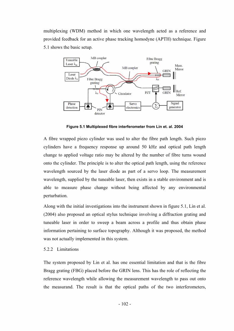
- 102 -
multiplexing (WDM) method in which one wavelength acted as a reference and
provided feedback for an active phase tracking homodyne (APTH) technique. Figure
5.1 shows the basic setup.
Figure 5.1 Multiplexed fibre interferometer from Lin et. al. 2004
A fibre wrapped piezo cylinder was used to alter the fibre path length. Such piezo
cylinders have a frequency response up around 50 kHz and optical path length
change to applied voltage ratio may be altered by the number of fibre turns wound
onto the cylinder. The principle is to alter the optical path length, using the reference
wavelength sourced by the laser diode as part of a servo loop. The measurement
wavelength, supplied by the tuneable laser, then exists in a stable environment and is
able to measure phase change without being affected by any environmental
perturbation.
Along with the initial investigations into the instrument shown in figure 5.1, Lin et al.
(2004) also proposed an optical stylus technique involving a diffraction grating and
tuneable laser in order to sweep a beam across a profile and thus obtain phase
information pertaining to surface topography. Although it was proposed, the method
was not actually implemented in this system.
5.2.2 Limitations
The system proposed by Lin et al. has one essential limitation and that is the fibre
Bragg grating (FBG) placed before the GRIN lens. This has the role of reflecting the
reference wavelength while allowing the measurement wavelength to pass out onto
the measurand. The result is that the optical paths of the two interferometers,
- 103 -
measurement and reference, are not identical. In this situation, the APTH method can
only stabilise the reference path, and as such disturbance in the measurement path
between the FBG and the measurand is unattenuated. This issue is compounded
because of the short length of fibre between the FBG and the GRIN lens, which is
uncompensated and much more sensitive to any environmental perturbation than an
air path of the same length.
The resulting system proposed cannot provide enough stability for accurate
measurement of surface topography. In order to develop such an instrument a better
method for stabilising the interferometer must be found, and in addition, the optical
stylus concept needs to be further investigated.
5.2.3 An Improved Method
In order to improve on the method described in section 5.2.1 it is necessary to reduce
the non-commonality of the reference and measurement optical paths. Figure 5.2
shows an experimental setup devised to improve performance by removing the FBG
from the measurement arm and allowing the reference beam to be incident upon the
surface. The device shall be henceforth known as a multiplexed fibre interferometer
(MFI) in the course of this thesis.

- 104 -
Figure 5.2 Multiplexed Fibre Interferometer Schematic

- 105 -
With this technique the only section at which the reference and measurement
interferometer paths are separate is at the diffraction grating. As such the different
optical paths cover only a short distance in air or the glass of the objective lens; both
these mediums are much more stable than optical fibre.
It can be seen in figure 5.2 that the instrument is not in actual fact a true all-fibre
interferometer given that the interference occurs upon the diffraction grating between
the retro-reflected first and zero order diffracted beams. In may be more correctly
termed a fibre sourced interferometer. The system is also inherently more stable as it
is essentially a bulk interferometer, but it maintains the advantages of a fibre link
allowing it to be remotely placed.
The over-arching methodology for the instrument shown in figure 5.2 is that twin
interferometers, running at different wavelengths, are near-common path throughout
the whole of the optical circuit. The next section considers the experimental setup in
some detail.
5.3 Apparatus
5.3.1 Overview
There are many elements to the experimental setup shown in figure 5.2, both of an
optical and electronic nature. This section gives an overall view of the path of optical
and electrical signals through the instrument. Detailed studies of the component parts
will be presented in subsequent sections. The optical path will first be considered and
the roles of the various components explained. Following that will be an overview of
the electronic part of the instrument.
For the initial investigations and proof of concept work, a mirror was used to
represent a surface. In optical terms this may be considered the ‘ideal’ surface,
having maximum reflectivity and minimal surface texture as the surface is polished to
within / 20λ at 632.8 nm.
5.3.2 Optical
Figure 5.2 highlights the various wavelengths present in the optical circuit by colour.
The reference interferometer wavelength ( 1550 nmrλ = ) is supplied by a laser diode

- 106 -
(Wuhan Telecommunications PDDM981) and enters port 1 of a 3 dB coupler. Light
from a tuneable laser source (Ando AQ4320D) provides the measurement
interferometer source ( 1555 1575 nmmλ = − ) and enters port 2 of the coupler. In this
way, the light exiting ports 3 and 4 of coupler A is wavelength division multiplexed
(WDM). The light exiting port 4 is dumped by placing the cleaved fibre end into
index matching gel to disperse the light harmlessly and minimise return loss. This
method of multiplexing results in approximately half of the source light power being
lost.
The multiplexed light is then incident on port 1 of circulator A and exits port 2,
where it exits the fibre. A GRIN lens then serves to collimate the light exiting the
fibre into free space where it is then incident on a blazed diffraction grating (Yvon
Jobin 5109720). This grating then diffracts the incident beam into a zero order
(reflected) beam and two first order beams. The zero-order beam is comprised of both
the reference and measurement interferometer wavelengths. First order diffraction
produces two angularly separated beams, consisting of the reference and
measurement wavelengths respectively.
The zero order beam is normally incident on the reference mirror and is thus retro-
reflected back to the same point on the grating from which it emerged. The angularly
dispersed first order beams are collimated using an achromatic doublet (Melles Griot
06 LAI007) upon the measurement mirror. The beams are reflected back from the
measurement mirror and then re-trace their path back to the grating where they
interfere with the returning zero order beam and are incident upon the GRIN lens
afterwhich they re-enter the fibre.
Interference takes place where the retro-reflected zero and first order beams
recombine at the grating. The resulting interfered beam then re-enters the GRIN lens
where it is focused back into the fibre.
The incident beam, containing both interfered multiplexed wavelengths, re-enters
circulator A at port 2 and exits at port 3. Here it enters circulator B at port 1, exiting
at port 2 where it is incident on the fibre Bragg grating (FGB). The FBG acts to
separate the reference and measurement wavelengths.

- 107 -
The reference wavelength ( 1550 nmrλ = ) coincides with the peak reflectivity
wavelength of the FBG and as such is reflected back in to circulator B at port 2 where
it exits at port 3 and is incident on PIN diode B. The measurement interferometer
wavelengths are passed by the FBG, with some attenuation, where they are then
incident on PIN diode A.
It is seen that circulator B and the FBG form a wavelength de-multiplexer which
separates the measurement and reference interferometer outputs onto PIN diodes A
and B respectively.
5.3.3 Electronics
The instrument contains numerous electronic modules which may be addressed in
any particular order. Signal flow is marked by the arrows in figure 5.2 from which
the labels in the following list are also taken.
I-V Amplifier
These are current to voltage converters, commonly known as transimpedance
amplifiers. They convert the photocurrents generated by their respective PIN
photodiodes into a voltage. The voltage output of the transimpedance amplifier is
proportional to the intensity of light exiting the fibre.
Servo Electronics
This module forms the basis for the active phase tracking homodyne (APTH) method
implemented to stabilise the instrument (see section 4.7.6). It is essentially a
proportional-integral (PI) controller which takes the voltage output from the reference
interferometer and compares it to a setpoint (or demand) voltage. It then applies a
voltage to the piezoelectric translator (PZT) stage in order to move the reference
mirror until the error is zero.
PC
The PC is used as the host for National Instruments Labview software.
NI PCI-GPIB
This is a National Instruments NI PCI-GPIB provides a GPIB (IEEE 488.2) interface
and controller on the host PC. This is used primarily for communication with the AQ

- 108 -
4320D and HP 8168F tunable lasers, as well as the Ando AQ6317 optical spectrum
analyser.
NI PCI-6221
This is another National Instruments multifunction data acquisition (DAQ) card. It
provides a means of acquiring analogue voltage signals at up to 250 kS/s, shared over
16 input channels with 16 bit resolution. In addition it can supply two analogue
voltage waveforms with an update rate of up to 833 kS/s at 16 bit resolution. It also
feature digital inputs/outputs. The NI PCI-6221 is used to provide the setpoint
voltage to the servo electronics and acquire the analogue voltage data from the
measurement interferometer.
PZT
The PZT serves to translate the reference mirror along the optical axis in order to
create a path length change in the both the reference and measurement
interferometers. It is actuated by a voltage applied to it from the servo electronics
module. The PZT model used is of the low voltage stack type having multiple,
parallel wired piezo elements whose individual translations are additive. This creates
a relatively large translation for small applied voltages at the expense of some other
attributes such as capacitance (which is increased). The model used is the PI 810.10
which has a translation of 15 μm over 100 V with a resolution of 0.15 nm.
5.4 Analysis of Instrument Performance
The operation of the multiplexed fibre interferometer may be understood by
considering it in four distinct sections. There is the surface to phase relationship, the
optical probe operation, the active stabilisation and the phase shifting method. This
next section will go through to analyse each element individually.
5.4.1 Surface Height to Phase Relationship
The aim of the instrument is to derive height data from the measurement surface
using an optical stylus. The response of the interferometer at a point x along a profile
on the surface is

- 109 -
( ) ( ) ( ) ( )1 2 cosI x I x I x V xϕ= + + (5.1)
where 1I and 2I are the intensities of the light returing from the reference and
measureand mirrors respectively. Taking the phase in the reference arm to be
constant it is found that the phase in the measurement arm is dependent only on the
surface height, h such that,
( ) ( ) ( ) ( )4 00
h x hx
πϕ ϕ
λ−⎡ ⎤⎣ ⎦= + (5.2)
where ( )0ϕ is the initial phase difference at the starting point on the profile and
( ) ( )0h x h− is the surface height difference at a point x also relative to that starting
point. The visibility term from (4.6) is
1 212
1 2
2 I IV g
I I=
+ (5.3)
which assuming the coupler has a perfect 50/50 splitting ratio, may be expanded to
take into account the various losses encountered within the optical circuit of which
the reflectivity of the measurand is of particular importance as this may vary
substantially between materials. The overall attenuation of the returning light
intensity is the product of twice the forward absorption coefficients, σ in each arm ,
the reflectivity, r of the measurand/reference mirror and the grating efficiency, effg
of the diffracted order.
1 0 1 12 effI I r gσ= ⋅ ⋅ (5.4)
2 0 2 22 effI I r gσ= ⋅ ⋅ (5.5)
All the coefficients in (5.4) and (5.5) will vary depending on the current position of
the optical stylus on the profile.
5.4.2 Optical Stylus by Wavelength Tuning
The optical stylus method relies on the tuning of the measurement interferometer
wavelength in order to sweep the light beam across the surface to take a profile of the
height variation. The method is very similar to that found in spectrometers whereby a

- 110 -
grating is used to angularly disperse an incoming light beam which is then collimated
onto a sensor. In the case of the optical probe in this instrument a tuneable laser is
used to change the wavelength over time meaning that the full laser power is
available at each profile position measured. Figure 5.3 shows a schematic of the
optical probe.
Figure 5.3 Optical probe schematic
The grating in the optical probe creates an angular dispersion which has a wavelength
dependence. This is a direct consequence of the grating equation
1sin sinmdλβ α− ⎛ ⎞= −⎜ ⎟
⎝ ⎠ (5.6)
where β is the diffracted angle, d the grating spacing, m the grating order and α
the angle of incidence. All angles are measured in relation to the grating normal as
shown in figure 5.4, the sign of the angle being dependent on which side of the
grating normal the angle is.

- 111 -
Figure 5.4 Angle sign definition for gratings
The collimating lens in the optical probe has the effect of collimating the angularly
dispersed light. The relationship between the angular dispersion and the length of the
scanned profile is given by the linear dispersion, which is commonly found in
spectrometer design equations. The magnitude of the linear dispersion of the beam
along the profile is given by
cos
x mfdλ β
Δ = ⋅Δ
(5.7)
where f is the effective focal length of the lens used. The cosine term in the
denominator of (5.7) requires that the diffracted angle be kept small in order to
maintain the linearity of the scan.
Equations (5.6) and (5.7) show that it is possible to vary the scan width using two
methods; by varying the angle of incidence α , or by changing the effective focal
length, f of the collimating lens. Clearly f is fixed for a given optical probe as the
lens must be physically changed and varying α may only be done over a short range
before the onset of non-linearity in scan.
It is worth pointing out that any non-linearity in the scan with wavelength is
systematic and there is thus scope for calibrating it out by either altering the
wavelength step during the scanning, or using a suitable method for interpolating the
scanned data.
The lens used to collimate the light was an achromatic doublet (Melles Griot 06
LAI007) having an effective focal length of 60.8m at an operating wavelength of
1550 nm. An achromatic doublet is used because it forms the smallest possible beam
spot size for a simple single element lens. The grating used (Yvon Jobin 5109720)
has groove density, 1/ d of 900 lines/mm which at 1550 nm limited the grating to
first order operation thus 1m = . The use of a blazed diffraction grating helps direct
more optical power in the first order diffraction beam which helps to counter the
attenuation caused by the measurand that will likely have a lower reflectivity than the
reference mirror.

- 112 -
0.00
0.10
0.20
0.30
0.40
0.50
0.60
0.70
0.80
0.90
1.00
0 10 20 30 40 50 60 70 80 90Angle of incidence, α (deg)
Line
ar D
ispe
rsio
n, ∆
x / ∆
λ (m
m/n
m)
Figure 5.5 Linear dispersion vs. beam angle of incidence, α
Figure 5.5 shows how the linear dispersion changes with the angle of incidence of the
grating beam. A numerical analysis of a scan point by point was carried out for a
wavelength sweep of 20 nm at various angles of incidence. The result in figure 5.6
shows clearly how the scan range and linearity are related. The scan range may be
increased to a degree at the expense of the linearity of the wavelength sweep.
0
2
4
6
8
10
12
1560 1565 1570 1575 1580
Wavelength, ¸ (nm)
Prof
ile P
ositi
on, x
25
25.5
26
27
30
α
Figure 5.6 Scan path linearity for various angles of incidence
In the initial experiments the incidence angle, α was kept such that the scan range
was approximately 3 mm, thus maintaining a good degree of linearity.

- 113 -
The zero order beam which is used to form the reference arm is the special case of
the grating equation (5.6) in which 0m = . Here we see that the wavelength
dependence disappears and only the specular component is left.
β α= − (5.8)
This means that as the wavelength is swept and the first order beam moves across the
optical profile, the reference beam will always remain stationary (Palmer 2005, pp.
20-44).
5.4.3 Active Disturbance Rejection
The problems of phase instability in fibre interferometers were outlined at length in
section 4.7.2. Here we see that the phase variation creates an error term which maps
itself upon the surface height information. This relationship can be described by the
addition of a random time varying phase term, ( )tε as shown in equation (4.24).
Considering for a moment the apparatus set up with just the reference wavelength
source enabled, the output of the interferometer is
( ) ( ) 0 1 cosrefI x I V tϕ ε= + +⎡ ⎤⎣ ⎦ (5.9)
where an error term, ( )tε describes the unwanted phase variation due to thermal and
acoustic perturbation. The active phase tracking homodyne method (APTH) as
described in section 4.7.6 can be used to stabilise the interferometer using the PZT
mounted mirror to change the reference arm path length. The PZT is able to translate
the mirror along the optical axis of the reference mean with the application of a
voltage.
A servo control loop may be considered in which the reference mirror is moved to
oppose the time varying error term in the phase. This may be implemented very
simply, if not optimally, with a PI controller tuned manually. An analysis of the
control loop may be done by first considering the individual elements as shown in
figure 5.7.

- 114 -
( )cG s ( )pztG s ( )pdG s( )ifG s ( )Y s( )U s
( )H s
Figure 5.7 Block diagram representation of the closed loop MFI
Control systems analysis is often carried out in terms of Laplace functions, where
s jω= and is the complex frequency. This has the benefit of converting differential
equations in to linear algebra and thus greatly simplifying the analysis.
Figure 5.7 shows the open loop transfer function (OLTF) in the s-domain (complex
frequency domain) in the general case of some controller having the transfer
function ( )cG s is,
( ) ( ) ( ) ( ) ( )c pzt if pdG s G s G s G s G s= (5.10)
( ) ( ) ( ), , pzt if pdG s G s G s are the transfer functions of the PZT/driver combination,
interferometer and photodiode/transimpedance amplifier combination respectively.
Consequently the closed transfer function (CLTF) is given by
( )( ) ( )1
G sCLTF
G s H s=+
(5.11)
with the feedback path, ( )H s being unity as it is a direct connection (Dorf & Bishop
1998, ch. 2).
Interferometer Response
The analysis of a control loop in terms of Laplace transforms may only be realised if
the system is linear time invariant (LTI). When considering the response of the
interferometer in (5.9) the fact that it is cosinusoidal means that the system is not
strictly an LTI system. However one may consider that in the ideal case the feedback
in the control loop will keep excursions of phase small. As such, a small signal
approximation to the response of the interferometer may be applied which is linear
over a small range (about quadrature) and thus LTI. This approximation results in the
modelling of ( )ifG s as a simple gain term.

- 115 -
The maximum gradient appears around the quadrature point and remains
approximately constant over small deviations from that point. The magnitude of the
gradient is simply the visibility,
1 2
1 2
2if if
I IG K
I I=
+ (5.12)
for the small signal case. The complex degree of temporal coherence, 12g is
approximated to unity since the coherence lengths of the sources are far longer than
the optical path lengths being considered. ifK can be considered to be a conversion
gain transforming optical path length in metres to power in Watts.
Piezo-electric Translator
The dynamic response of a PZT is very complex due a combination of inherent non-
linearities and the mechanical dynamics involved with moving the mass of the
mirror. PZTs exhibit several undesirable characteristics including hysteresis, non-
linear voltage-displacement response, drift and creep. They also have an asymmetric
force supplying capability, and unless pre-tensioned with a compressive spring force
are able to supply much more push than pull. The mass of the mirror mounted upon
the PZT results in finite settling times due to the interaction of the mass and the
stiffness of the piezo element. This is of particular relevance in phase stepped
techniques where the mirror is moved into different positions.
mass, m
damping, ζPZT
stiffness, k
Figure 5.8 Equivalent representation of a PZT
Figure 5.8 shows the approximated equivalent system to be used for the analysis. The
mechanical response of the PZT is considered to be a spring-damper system with an
attached mass. The s-domain representation is given by,

- 116 -
( )2
2 2n
nPZT
nQ
G ss sω
ωω
=+ +
(5.13)
which is familiar as a second order system with nω being the resonant frequency
(rad) while Q is the quality factor which describes the sharpness of the resonance.
The quality factor is related to the damping ratio, 1/ 2Qξ = . It is found that the
resonant frequency is governed by the mass, m and the stiffness of the piezo
material, k such that
nk
mω = (5.14)
It is possible to derive an unloaded mass, 0m from (5.14) for an unloaded PZT with
datasheet values for stiffness and resonant frequency (Hicks & Atherton 1997). The
effective mass for a PZT loaded with a mass, m is then 0effm m m= + . It should be
noticed that the small scale stiffness values are often larger than the large scale
stiffness values so the appropriate value for the situation must be used.
For the PI-810.10 PZT having large signal stiffness, 18.6 N/μmk = and resonant
frequency of 22 kHz it is found that 10 0.977 x 10m −= kg.
A Bode plot of the transfer function, ( )pztG s was produced using Matlab for the PI-
810.10 PZT investigated and is given in figure 5.9. The mass of the small mounted
mirror was found to be 31x10 kg− thus the effective mass, 31.977 x 10 kgeffm −= .
The quality factor is unknown but it shall be seen that this does not hold too much
importance when the device is used well below resonance. Here, an arbitrary value
10Q = is chosen order to make clear the effect on the frequency response (Physik
Instrumente 2005).

- 117 -
104 105 106-50
0
50
Mag
nitu
de (d
B)
Bode Diagram
Frequency (rad/sec)
0 0.2 0.4 0.6 0.8 1 1.2
x 10-3
0
0.5
1
1.5
2Step Response
Time (sec)
Am
plitu
de
Figure 5.9 Simulated Bode plot and step response for a PZT
It is seen from figure 5.9 that the additional load of the mirror has lowered the
resonant frequency from 22 kHz to 15.5 kHz. It may be seen from the normalised
step response that the quality factor or degree of resonance has a large effect on the
settling time.
Slew Rate Limiting
Another important parameter of PZT performance is the maximum slew rate
obtainable in operation. In practice it is this limitation that generally impinges upon
the stability of a control loop before the resonant behaviour. Slew rate limitations can
arise from two sources, the maximum push/pull force produced by the PZT in order
to accelerate the load mass and the current driving (compliance) limits of the drive
electronics.
Push/Pull Limiting
The main limitation on the frequency response of the feedback system overall is the
limited slew rate of the piezoelectric actuator used to move the mirror. For dynamic

- 118 -
operation, a PZT must provide enough force to create the required acceleration on the
mirror mounted upon it. This force is given by,
2 242dyn effLF m fπ Δ⎛ ⎞= ± ⋅ ⎜ ⎟
⎝ ⎠ (5.15)
The current PI-810.10 PZT has a maximum stopped push force of 50 N. However,
piezo-electric elements are much less efficient at contracting and thus the maximum
pull force is found to be much lower at 1 N. The maximum non-slew rate limited
sinusoidal frequency is given by,
max 22dyn
eff
Ff
m Lπ ⋅
=⋅ Δ
(5.16)
The effective mass, 31.977 x 10 kgeffm −= was derived earlier, and 1 NdynF = is the
lower limit as produced by the maximum pulling force of the PZT. The limit on the
peak to peak displacement, 3.6 μmLΔ = is given by the product of the displacement
to voltage ratio (0.15 μm/V) and the maximum voltage range (24 V), which is limited
by the drive electronics (Physik Instrumente 2009).
An evaluation of equation (5.16) suggests max 2.67 kHzf = as the large signal worst
case value. For the small signal case which we can define as being one full fringe, or
approximately 775 nm at an operating wavelength of 1550 nm, we might expect a
maximum undistorted frequency of about 5.75 kHz.
Current Limiting
The peak sinusoidal frequency that may be obtained by using PZT drive electronics
supplying maximum current, maxi over a peak to peak voltage range pk pkV − is given
by,
maxmax
pzt pk pk
ifC Vπ −
=⋅ ⋅
(5.17)
In the PZT drive electronics used in this apparatus, the BUF624T current driver can
supply max 250 mAi = which over 24 Vpk pkV − = (limited by the LF355 op amp
operating range) yields the large signal case of max 9.2 kHzf = . The small signal case

- 119 -
is somewhat higher, to move one full fringe at 1550 μm requires a voltage shift of
5.17 V, yielding max 42.8 kHzf = (Burr Brown 1996).
It is clear from these design calculations that the PZT slew rate is not limited by the
drive electronics and we may consider the maximum push/pull rate to be the limiting
factor. Slew rate limiting is not easily and simply modelled using s-domain methods
as it is an inherently non-linear function. In general the effects of slew rate limiting
on a control loop can be disastrous and it is usually avoided by ensuring that the slew
rates of any controller are smaller, thus avoiding integral windup (Pickelman 2003).
Photodiode Front-end
The photodiode and transimpedance amplifier transfer function, ( )pdG s is generally
well modelled as a multi-pole response produced by the interaction of shunt
impedance at the input and the feedback impedance along with the open loop gain
profile of the op amp used. A detailed circuit analysis is involved and as such is given
separately in appendix A. Good design will ensure that the response of the
photodetector front end is sufficient enough not to limit the performance of the
control loop while at the same time ensuring the minimum bandwidth in order to
minimise noise on the output. The general transfer function for a transimpedance
amplifier and photodiode front end is derived in appendix A.1 and is
( ) ( )( ) ( )
( )1 f
sh
ol ftrans z s
z sol
A s z sz
A s=+ +
(5.18)
The voltage produced by a transimpedance amplifier for a photocurrent of phi from a
reverse biased photodiode is given by,
out ph fV i R= (5.19)
In other words the value of fR sets the DC transimpedance.
The responsivity of the PDDM981 PIN photodiode used in this instrument is given as
1.05 A/W at a working wavelength of 1550 nm (Wuhan Telecommunications). The
maximum input voltage range of the NI PCI-6221 DAQ card is ±10 V (National
Instruments 2007). With the losses of the optical system unknown initially, a suitable
value for the transimpedance was required and this was carried out experimentally.

- 120 -
The idea was to present a reasonable voltage range for the normal operating
conditions. The reference transimpedance amplifier was initially designed with a 50 k
variable resistor and a 10 pF feedback capacitance in which provided fairly heavy
damping to the response, ensuring consistent stability over the transimpedance
operating range. This resulted in manageable working output voltages of up to 0-5 V
in practice.
An analysis using a Matlab script (see appendix C) was carried out, the frequency
and step responses are shown in figure 5.10.
100 101 102 103 104 105 106 107 1080
2
4
6x 10⁴
Cur
rent
Gai
n (a
bs)
Bode Diagram
Frequency (Hz)
0 0.5 1 1.5 2 2.5 3
x 10-6
0
2
4
6x 10⁴ Step Response
Time (sec)
Am
plitu
de
Figure 5.10 Simulated Bode-magnitude plot and step response for a transimpedance amplifier
For the case of the circuit used as a transimpedance amplifier in this apparatus it will
be seen that that any poles of the transfer function are at frequencies several orders of
magnitude higher than those of the PZT actuator. Hence these poles have negligible
effect on the overall system transfer function and as such the transfer function may be
usefully modelled as the simple DC transimpedance given in (5.19), in which case,
pd pd fG K R= (5.20)

- 121 -
In this way pdK may be considered as a conversion gain, changing intensity to
voltage.
The Controller
With the all the contributing elements in the forward path or plant approximately
characterised it is worthwhile revisiting (5.8) and rewriting the forward path
( ) ( ) ( )c pzt if pdG s K s K s K K= ⋅ ⋅ ⋅ (5.21)
which now includes the approximation of the photodiode front end and small signal
interferometer responses as simple gain terms.
The requirement now is to select a controller which when employed in the forward
path, will allow for the reduction of external disturbance affecting the closed loop
system. Figure 5.11 shows the block diagram of the closed loop system with a
disturbance source ( )D s representing unwanted optical path length variation in the
loop.
( )cG s ( )pztG s pdK
( )D s
ifK ( )Y s( )U s
Figure 5.11 Block diagram representation of the closed loop MFI with the addition of an external disturbance
The method for quantifying the level of disturbance rejection in a control loop is by
defining a sensitivity transfer function, DGS which describes the output response of
the system to a given disturbance signal,
( )( )
GD
Y sS
D s= (5.22)
The open loop transfer function from figure 5.11 is simply ( ) if pdG s K K= and the
feedback path is ( ) ( ) ( )c pztH s G s G s= ⋅ . With reference to equation (5.22) the closed
loop transfer function is then

- 122 -
( )( ) ( ) ( ) ( )1 1
if pdGD
if pd c pzt
K KG sS
G s H s K K G s G s= =+ +
(5.23)
The sensitivity, DGS is the main figure of merit for analysing the effectiveness of this
system to reducing the influence of environmental perturbation. Equation (5.23)
shows that increasing the gain of the controller ( )cG s will in general improve the
disturbance rejection assuming of course that the closed loop system remains stable.
The obvious initial choice for a controller ( )cG s is that of a proportional-integral
controller since it is easy to implement and generally robust in operation if the
parameters are correctly chosen. A PI controller can provide effective control which
is easily implemented, by virtue of having only two parameters, by analogue
electronics.
The PI control is essentially a simplification of the common proportional-integral-
differential (PID) controller with the derivative term set to zero. There are various
PID controller structures which have varying historical reasoning behind them. These
are the ideal (or non-interacting), series and parallel forms. The parallel form is the
most general as the three actions are completely separated and as such the integral
term to be turned off if necessary. Its transfer function is
ic p d
KG K K ss
= + + (5.24)
where pK , iK and dK are the gains of the proportional, integral and differential
elements respectively. The integration time, iτ is sometimes used to refer to the
integration gain where 1/i iK τ= (Visioli 2006, pp. 1-18). The analogue electronic
implementation of the parallel PI controller ( 0dK = ) used in this apparatus is given
in appendix B.2.
Given the implementation of a PI controller as the closed loop compensator it is now
possible to analyse the effectiveness of the control loop and load disturbance due to
environmental perturbation. For the purpose of this analysis it was decided to set the
gain 3if pdK K⋅ = which is equivalent to a 3V peak-to-peak interference fringe and
was found to be reasonable in practicality.

- 123 -
5.4.4 Control Loop Analysis
The overall control may be usefully studied in Matlab which eases computation and
provides access to useful graphical routines such as bode plots step responses.
Appendix D.3 shows the Matlab script used to study the control loop, the variable
nomenclature relates to that used in the previous sections.
There are two control parameters to consider, the proportional and integral gains, pK
and iK respectively and also one unknown parameter Q. It is important that the
integral gain is kept equal to or smaller than the maximum slew rate available by the
PZT actuator, thus 35.75 x 10iK = is the simulation value set which is the maximum
to allowable for predictable simulation results.
-80
-60
-40
-20
0
20
40
Mag
nitu
de (d
B)
100 101 102 103 104 105 106-45
0
45
90
135
Pha
se (d
eg)
Kp=0.1
Frequency (rad/sec)
Ki=1 kHzKi=2 kHzKi=3 kHzKi=4 kHzKi=5.75 kHz
Figure 5.12 Simulated Bode plot of the sensitivity function for varying integration gains
Figure 5.12 shows the frequency response of the sensitivity function, GDS with
varying amounts of integration gain for a static proportional gain of 0.1. It is very

- 124 -
clear that increasing the integration directly improves the disturbance rejection. It
also however appears to amplify any component around the resonant frequency.
-80
-60
-40
-20
0
20
40M
agni
tude
(dB)
100
101
102
103
104
105
106
-45
0
45
90
135
180
Phas
e (d
eg)
Kp=0Kp=0.001Kp=0.01Kp=0.1Kp=1
Figure 5.13 For varying proportional gains
Figure 5.13 shows the frequency response of the sensitivity function, GDS with
varying amounts of proportional gain. It would appear that changing the proportional
gain does nothing to alter disturbance rejection at low frequencies, however at high
frequencies it appears to help. It also appears to amplify the resonance, although the
slew rate limit, not modelled here must also be limiting. It is noticed in the step
response that the higher the proportional gain, the more distortion seen in the initial
‘kick’ of the step response. Too much proportional gain actually appears to slow
down the step response.
The consequence of slew rate limiting is not included in the model due to the fact it is
not a linear function, nor is it easily linearised. In this sense it is an unknown element
and will cause instability if the actuator is driven above the slewing frequency. The
best technique for ensuring stability is to ensure the integration gain remains below
the slew rate limiting frequency.

- 125 -
The mathematical analysis of the control loop gives a strategy for implementation of
the PI settings. The integration gain is the primary method of reducing load
disturbance so the critical action is to raise this as high as possible with any
improvement possible with the proportional element of the control being secondary.
Obviously all the considerations for improving the disturbance rejection qualities are
dependent on the closed loop stability. There are several tests used in control theory
to determine whether a closed loop system will be stable including phase/gain
margins, Nyquist and root loci plots. Frequency domain methods are intuitive and
clear and a gain-phase plot can show clearly the ramifications of parameter variation
on a system. In a gain-phase plot, the gain and phase value of the open loop function
are plotted with changing frequency (Dorf & Bishop 1998, ch. 9).
The phase margin is defined as the amount of phase shift the will result in a
marginally stable closed loop system. A marginally stable closed loop system will
occur when the phase of the open loop transfer function is 180° at the unity gain cross
over frequency. The critical factor for stability is to ensure that the phase margin does
not reach zero, indeed for a system robust to parameter variation in the plant it is
preferable that it should be no less than 30°, above this gain peaking will occur and
an under damped closed loop response observed.

- 126 -
Kp=0.1
Open-Loop Phase (deg)
Ope
n-Lo
op G
ain
(dB)
-360 -315 -270 -225 -180 -135 -90 -45 0-60
-50
-40
-30
-20
-10
0
10
20
30
40
6 dB 3 dB
1 dB 0.5 dB
0.25 dB 0 dB
-1 dB
-3 dB
-6 dB
-12 dB
-20 dB
-40 dB
-60 dB
Ki=1 kHzKi=2 kHzKi=3 kHzKi=4 kHzKi=5.75 kHz
Figure 5.14 Simulated Nichols chart of the open loop response of the MFI for varying values of integration gain.
Figure 5.14 shows a Nichols (gain vs. phase) plot for ( )G s for varying levels of
integral gain. The phase margin on the plot is given by the horizontal distance
between the cross-haired point (where the phase is 180° and the gain 0 dB) and the
curve. It is clear that if at any point the curve crosses into the quadrant above and to
the left of the cross-haired point and unstable system will result. For the results given
in figure 5.14 it can seen that the closed loop system should always be stable even
when the integral gain is turned up to the slew rate maximum of 5.75 kHz (as
imposed earlier). This is confirmed by examining the closed loop step response
shown in figure 5.15. The beginnings of instability (gain peaking) are produced at the
highest value of integration gain however indicating a marginal situation.

- 127 -
0 0.5 1 1.5 2 2.5
x 10-3
0
0.2
0.4
0.6
0.8
1
Kp=0.1
Time (sec)
Am
plitu
de
Ki=1 kHzKi=2 kHzKi=3 kHzKi=4 kHzKi=5.75 kHz
Figure 5.15 Simulated closed loop response of the MFI to a setpoint change
5.4.5 Extraction of Phase Data
Extraction of phase data from the output of an interferometer is non-trivial due to the
co-sinusoidal nature of the response. PSI is one solution for retrieving the absolute
phase value from an interferogram and is suitable for determining the absolute (DC)
phase value (see section 4.7.8). The phase is manually shifted to various points and
the output interferogram recorded at each point. A suitable algorithm may then be
used to determine the actual value of the original phase (Creath 1988).
For this instrument, PSI techniques were used to retrieve the phase information from
the interferometer using the Carré algorithm (Carré 1966). This algorithm was used
in preference to others because it is unique in the fact that it does not require a known
phase shift to be performed. This is clearly a great advantage in this system as the
shifting of the mirror will induce a different magnitude of phase shift in each of the
wavelengths scanned to gain the whole scan profile. The only requirement in the use

- 128 -
of the Carré algorithm is to ensure is that each phase step created by the mirror i.e.
the distance the mirror is moved, is identical with each phase step.
If ( )xϕ is the original phase at a sampled point x on the scan profile, the phase is
altered by 4 equal steps, 3 , , and +3α α α α− − + around this point and 4 intensity
values 1( )I x , 2 ( )I x , 3 ( )I x and 4 ( )I x respectively are obtained. These are then input
into the Carré algorithm to yield the original phase value at each point. The Carré
algorithm is given by,
( )( )( )
2 3 1 4 1 2 3 412
1 2 3 4
3 3tan
I I I I I I I II I I I
ϕ − − − + + − −=
− − + (5.25)
where the dependence on x is dropped for clarity.
5.5 Implementation
5.5.1 Practical Implementation of PI Control
The physical implementation of the PI controller used in this apparatus was done
using op amps throughout; the details are given in appendix B.2. The circuit was
designed to supply a variation of proportional and integral gains through variable
resistors, allowing the circuit to be tuned. The poles of the operational amplifiers
formed by feedback impedances, open loop gain roll off etc. are all found at much
higher frequencies than the dominant dynamics of the control loop and are thus
neglected. The reasons for this are outlined in description of the transimpedance
amplifier in section 5.3.3.
Tuning of the PI circuit was done by mounting the measurement mirror on a second
PZT and applying a sinusoidal waveform from a signal generator, while the reference
interferometer output was observed. The integration and proportional gains were then
adjusted to minimise the peak to peak disturbance of the reference interferometer.
The setup of the optical probe to facilitate this is shown in figure 5.16.

- 129 -
Figure 5.16 Schematic of the optical probe with added PZT to apply disturbance to the measurand
5.5.2 Closed Loop Control to Implement PSI
Along with disturbance rejection, the closed loop PI control was used to shift phase.
This is made possible by changing the setpoint voltage applied to the control so that
the mirror is moved and another point on the fringe is locked. The resulting path
length change due to mirror movement also induces phase shift in the measurement
interferometer. By altering the setpoint voltage, it is possible to move the mirror
inbetween each profile capture whilst maintaining the disturbance correction. As such
a number of phase shifted profiles may be captured in a sequence.
There are two great advantages in using closed loop control for phase shifting. First,
the phase shift may be performed very accurately due to the closed loop nature of the
system. This also means that the nonlinearities of drift and hysteresis in the PZT do
not affect the accuracy of the shift. The other advantage is that that disturbance
rejection is continually ongoing during the whole measurement process.
Looking at the Carré algorithm (5.25) it is seen that 4 intensity measurements at
different reference mirror positions are required in order to derive the phase encoded
height profile of the surface. The literature suggests that the most effective phase shift
angle for the rejection of noise induced by phase shifting error is 110º. This is
equivalent to setting 55α = ° (Kemao et al. 2000).

- 130 -
From equation (5.2) the distance the reference mirror will have to move in produce
the required shifting of the phase term is
4
x ϕλπ
= (5.26)
The reference interferometer operating wavelength, 1550λ = nm requires a mirror
shift of 236.8 nm to produce the 110º phase shift. As the measurement wavelength
varies during the sweep, the magnitude of the phase step for the measurement
interferometer will vary across the profile. This is the reason for using the Carré
algorithm. Any other algorithm would require the induced phase step to be mapped
across the sweep.
5.5.3 Sequence of Operation
Figure 5.17 shows a functional representation of the non-optical elements of the
apparatus. It shows the PC running LabView controlling the Ando AQ4320D tunable
laser via a GPIB bus. The NI-PCI 6221 DAQ card is used to sample and digitise the
output of the measurement interferometer.
Each of the elements of the PI controller and PZT driver is also represented and
detailed circuit diagrams are provided in appendix B.
Figure 5.17 Functional diagram of the MFI

- 131 -
The DAQ card provides an analogue setpoint voltage to the PI controller with which
to control the phase shifted position. It also supplies TTL compatible logic levels to
provide:
Invert Enable - a setpoint inversion function to enable the controller top move to
phase shift positions 3 and 4.
Integrator Reset – Allows the integrator to be reset remotely, in the case of full scale
range being reached. When activated the integration capacitor is shorted and the
interferometer locks back on to the nearest setpoint value when re-enabled.
Setpoint Disable – Disconnects the control signal from the PZT. Used during fringe
visibility calibration.
It is useful to consider the flow of events that are taken when the apparatus is used to
take a measurement. This is given by the flowchart in figure 5.18, while the
following sections explain each element in more detail.
Initialise tuneable laser and DAQ
Get fringe visibility
Sweep tuneable laser
Enable stabilisation and move to first phase shift
Change setpoint to required phase shift
Sample measurement interferometer output
Align measurement data
Apply Carréalgorithm
Unwrap phase
x4
Initi
alis
atio
nM
easu
rem
ent
Pos
t Pro
cess
ing
Figure 5.18 Event flow of MFI during the measurement cycle
Initialise Tuneable Laser and DAQ Card.

- 132 -
First the tuneable laser and DAQ are initialised and set to known states ready for
wavelength sweeping. At this stage, parameters such as wavelength sweep range,
starting wavelength and power may all be selected.
Get Fringe Visibility
In order to apply the correct phase steps using closed loop control it is necessary to
determine the setpoint voltages that must be applied. A calibration routine was found
to be necessary to determine the visibility of the interferometer and thus determine
the correct setpoint voltages.
With reference to equation (5.9) if the visibility, V of the interferometer and the
quadrature point intensity are known it is possible to determine the setpoint voltage
changes needed to perform the required shift.
This was be done by disabling the closed loop controller and then applying a simple
triangle wave to the PZT. The amplitude of triangle wave was such that its peak to
peak voltage was sufficiently high enough to move the mirror over several fringe
multiples and as such a sinusoidal intensity response was produced at the output of
the interferometer. This in turn was registered as a voltage waveform on the DAQ
card which was then stored.
The peak values on the recorded response were then calculated by taking an average
of the all the low and high values. This act yields the low and high peaks, pk hiV − and
pk loV − respectively. The following formula then describes the voltage to phase
relationship of the reference interferometer;
[ ]1 cos2
pk hi pk loout pk lo
V VV V ϕ− −
−
−= + + (5.27)
Also the quadrature point voltage, when 90ϕ = ° is given by,
2
pk hi pk loquad pk lo
V VV V− −
−
−= + (5.28)
outV is the voltage output seen by the DAQ card for any given phase value, ϕ . The 4
setpoint values, relating to the 4 mirror shift positions were then found by simply
calculating outV for -110°, -55°, +55°, +110°ϕ = . These values then relate to the

- 133 -
required shift around the quadrature point, 90ϕ = ° . The phase step of 55% is found
the be the most effective for the reduction of random amplitude due to noise (Qian et
al. 2004).
-1
-0.8
-0.6
-0.4
-0.2
0
0.2
0.4
0.6
0.8
1
Quadrature point
Phase Shift Point
Quadrature point
Phase Shift Point
-55°
+55°+110°
-110°
236.8nm
Ref
. I/
F O
utpu
t Vol
tage
236.8nm 236.8nm
Figure 5.19 Response of the interferometer with the required setpoints shown (angles are relative to the quadrature point)
Figure 5.19 shows a representation of the intensity fringe with the calculated setpoint
values as red spots and the mirror shift distance required to step between them. The
quadrature voltage point is shown as a green spot.
Phase stepping is thus enabled by changing the setpoint voltage to the relevant
calculated value before the wavelength swept intensity profile from the measurement
interferometer is taken. This will yield the required 4 sets of intensity samples,
relating to the measured profile of the surface.
Changing Setpoint to Required Phase Shift
The setpoint shifting required a combination of hardware and software control (via
Labview). The required setpoint voltages are obtained by the visibility routine before
the measurement cycle begins. The voltages are output from the DAQ card to the
controller circuit (the setpoint input on figure 5.17). The actual shift order used is
slightly different from figure 5.19 shown previously.

- 134 -
Figure 5.20 Shift order of the setpoints during the measurement cycle
The measurement cycle starts by setting the mirror at the quadrature point. The
measurement cycle then proceeds as follows;
Shift 1 - Reduce the setpoint, get α− profile, 2 ( )I x .
Shift 2 - Increase the setpoint, get α+ profile, 3 ( )I x .
Shift 3 - Invert error signal, reduce setpoint, get 3α+ profile, 4 ( )I x .
Shift 4 - Reduce setpoint, get 3α− profile, 1( )I x .
It should be noted that for shift 4 that the mirror is not actually in the 3α− position
but 775 nm (one full fringe) in front of it. However as the response is modulo 2π the
intensity profile is identical for the purposes of the Carré algorithm.
The inverting of the setpoint is used to ‘push’ the setpoint over peak onto the
opposite side of the response. A unity gain inverter is used to perform this task, it
may be switched into the control circuit from a command in the Labview routine.
Align Measurement Data
After the measurement cycle was complete and the 4 intensity profiles were obtained
it was found that the sample sets were not precisely aligned. The reason for this is
that the start of the tuneable laser wavelength sweep is not precisely synchronised
with the start of the sampling. This occurrence stems from the non-deterministic
nature of the operating systems of the computer, the laser and the GPIB interface
over which the start-sweep command issued. As a result there is a variable time delay

- 135 -
between the start of the sampling and the start of the laser sweep. It was thus
necessary to post process the obtained intensity profiles in order to fully synchronise
their elements.
An analogue voltage output is available from the Ando AQ4320D tuneable laser that
is proportional to the current swept wavelength and this was used as the basis for
aligning the scanned data. During a wavelength sweep this output was sampled
simultaneously with the measurement interferometer intensity data using the
multiplexed input feature of the DAQ card. The resulting sampled data is stored in a
2D array of data, with one row containing the intensity samples from the
interferometer and the other containing the analogue voltage output from the tuneable
laser (Ando Electric Co 1999). An example of the waveform sampled from the
tuneable laser is shown figure 5.21.
Output from TLS Analogue Out during Wavelength Scanning
-0.5
0
0.5
1
1.5
2
2.5
0 0.4 0.8 1.2 1.6
Time (sec)
Volta
ge O
utpu
t (V)
Figure 5.21 Output of the tuneable laser analogue output during wavelength sweeping
The sampling is started before the tuneable laser sweep command is issued and
carries on after the sweep finishes in order to ensure a full capture of the sweep. The
actual intensity data required occurs only during the ramped section of the output
shown in figure 5.21. By aligning the ramps data values of all 4 sample data sets, it is
possible to synchronise the intensity sample sets at the same time, as long as the
operation is identically performed on both rows of each 2D array. The method used
was to cross-correlate the tuneable laser output sampled datasets 2 ( )I x , 3 ( )I x , 4 ( )I x
individually with data set 1( )I x . The discrete form of the cross-correlation function is
defined as,

- 136 -
( )i j i jj
f g f g∗ +∗ =∑ (5.29)
where jf ∗ is the complex conjugate of the sample value jf which in this case are
always real values.
In essence, it moves the dataset [ ]g j over the dataset [ ]f j sample wise in steps of i .
After each shift, the corresponding sample points are multiplied together and all the
results are summated. Clearly, when the two signals are closely matched there will be
a peak in the cross-correlation signal at that point. So the value of i at the peak of
( )if g∗ provides the number of shifts required to bring the intensity datasets back in
line.
After obtaining the number of samples needed to shift each of the datasets
2 ( )I x , 3 ( )I x and 4 ( )I x that number were simply removed from the front of the
datasets, thus bringing them into line. There must of course be some error associated
with this method especially as the analogue output from the tuneable laser is of a low
quality, uncalibrated and quite noise prone. Any error will become more relevant as
the lateral resolution of the system is increased, by reducing the beam spot size, and
this would need to be considered carefully.
The final stage of pre-processing the sampled datasets is to detect the start of the scan
by running a threshold detector over the tuneable laser analogue output. When the
threshold is exceeded (at the start of the ramp) then this is deemed to be the first
sample on the scan. The next 10 000 samples are isolated and retained (10 kHz
sample rate with 1 second wavelength sweep duration) from each data set. The result
is an aligned set of intensity profiles, in the form of a 4 row array, with which to pass
to the Carré algorithm.
Apply Carré Algorithm
The implementation of the Carré algorithm in LabVIEW consists of two parts; the
actual phase calculation and a method to remove the phase ambiguity. The phase
ambiguity results from the nature of the arctangent calculation in (5.25). The phase
can only be determined modulo π using this algorithm on its own. We can determine
the phase modulo 2π by examining the signs of the quantities proportional to sinϕ

- 137 -
and cosϕ . The rules given in table 5.2 are then used to adjust the original calculated
phase value to ensure it lies in the correct quadrant.
sinϕ cosϕ Adjusted Phase
Positive Positive ϕ
Positive Negative π ϕ−
Negative Negative π ϕ+
Negative Positive 2π ϕ−
0 Anything π
Positive 0 / 2π
Negative 0 3 / 2π
Table 5.2 Rules for determining arctangent quadrant for the Carré algorithm
For the Carré algorithm, the quantities that must be examined are:
( )2 3( ) ( ) sinI x I x ϕ− ∝ (5.30)
( ) ( )2 3 1 4( ) ( ) ( ) ( ) cosI x I x I x I x ϕ+ − + ∝ (5.31)
Unwrap Phase
After the Carré algorithm has been executed, a phase unwrapping algorithm was run.
This provides a method of increasing the measurement range for slowly varying
surface heights (i.e. gentle slopes). It is a commonly used technique in
monochromatic phase shifting interferometry, and works by detecting for phase steps
values greater than π between adjacent sample values. If such a gap is detected, 2π
is added on (of taken off if the difference is negative) all proceeding samples. It is
necessary for the phase unwrapping technique to work that there are no actual jumps
greater than π between adjacent pixels and thus the technique is limited to gently
sloping surfaces. Another problem is sensitivity to measurement noise around the
upper and lower (0 and 2π ) points on the fringe, where a small amount of noise can
trigger a wraparound (Creath 1988).
5.6 Experimental Results
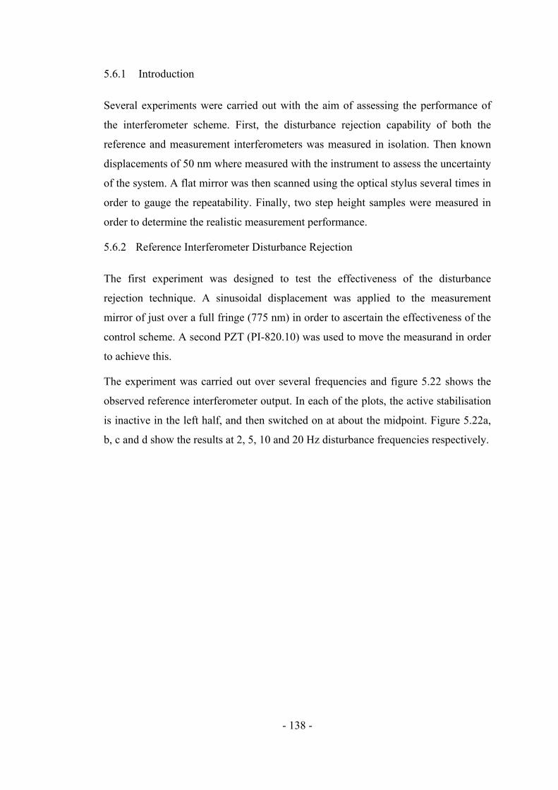
- 138 -
5.6.1 Introduction
Several experiments were carried out with the aim of assessing the performance of
the interferometer scheme. First, the disturbance rejection capability of both the
reference and measurement interferometers was measured in isolation. Then known
displacements of 50 nm where measured with the instrument to assess the uncertainty
of the system. A flat mirror was then scanned using the optical stylus several times in
order to gauge the repeatability. Finally, two step height samples were measured in
order to determine the realistic measurement performance.
5.6.2 Reference Interferometer Disturbance Rejection
The first experiment was designed to test the effectiveness of the disturbance
rejection technique. A sinusoidal displacement was applied to the measurement
mirror of just over a full fringe (775 nm) in order to ascertain the effectiveness of the
control scheme. A second PZT (PI-820.10) was used to move the measurand in order
to achieve this.
The experiment was carried out over several frequencies and figure 5.22 shows the
observed reference interferometer output. In each of the plots, the active stabilisation
is inactive in the left half, and then switched on at about the midpoint. Figure 5.22a,
b, c and d show the results at 2, 5, 10 and 20 Hz disturbance frequencies respectively.

- 139 -
Figure 5.22 The effect of the active stabilisation for varying frequencies
The left hand side of each plot shows the free running interferometer with the
stabilisation turned off and examination confirms that the induced sinusoidal
disturbance is indeed over a full fringe, the folding over of the fringe is quite clear at
the peaks. The righthand side of each plot shows the interferometer output when the
stabilisation control turned on.
The results seen in the diagram show quite clearly the effectiveness of the control
loop at attenuating load disturbance at the reference interferometer. At the point at
which the active stabilisation is enabled there is a transient response, after which the
output variation appears to be much diminished.
Qualitative inspection of the stabilised portions for each plot in figure 5.22 suggests
that the amount of residual disturbance in the output increases with frequency. This is
- 140 -
to be expected if one considers the analysis given in section 5.4.4 and specifically the
results shown in figure 5.12.
Figure 5.23 shows the corresponding control voltage for each of the cases shown in
figure 5.22. The square wave on the left hand portion of each graph is the open loop
response of the control due to the control loop being open (de-activated).
0 1000 2000 3000 4000-15
-10
-5
0
5
10
152 Hz
Con
trol S
igna
l (V
)
Sample No.0 500 1000 1500 2000
-15
-10
-5
0
5
10
155 Hz
Con
trol S
igna
l (V
)Sample No.
0 500 1000-15
-10
-5
0
5
10
1510 Hz
Con
trol S
igna
l (V
)
Sample No.0 500 1000 1500 2000 2500
-15
-10
-5
0
5
10
1520 Hz
Con
trol S
igna
l (V
)
Sample No.
Figure 5.23 Actuating signal from PI controller for varying frequencies
Figure 5.22 and figure 5.23 demonstrate how the control loop works to reduce load
disturbance in the reference interferometer. In order to gauge its effectiveness in
more quantitative terms an experiment was carried out similar to the previous one in
which the measurement mirror was sinusoidally displaced at various frequencies. The
peak to peak displacement was approximately 300 nm. At each frequency the free-
running peak to peak amplitude, fV and stabilised peak to peak amplitudes, sV were
recorded. The ratio of these gives the effective attenuation at each frequency where,

- 141 -
10Attenuation (dB) 20log f
s
VV
⎛ ⎞= ⎜ ⎟⎝ ⎠
(5.32)
Figure 5.24 shows the results of the experiment in graph format. The trend is of
steadily reduced attenuation with increased frequency as anticipated in the analysis in
section 5.4.4.
0
2
4
6
8
10
12
14
1 10 100 1000
Frequency of Applied Disturbance (Hz)
Atte
unat
ion
(dB)
Figure 5.24 Attenuation of sinusoidal disturbance with increasing frequency
This is an important result which verifies the possiblility of stabilising a fibre
interferometer using a reference interferometer operating at a separate wavelength.
The magnitude of the attenuation represents the effectiveness of the disturbance
rejection. The flattening of the response curve at lower frequencies is likely to be due
to the noise floor of the interferometer and control loop being reached. Theoretically
the response should continue to rise as the frequency goes down.
5.6.3 Measurement Interferometer Disturbance Rejection
It would appear from experimental results in the preceding analysis that the reference
interferometer is stabilised by the control loop and that the effectiveness of this
stabilisation is, as anticipated, dependent upon the disturbance frequency. It is also
necessary however to determine the long term stability of the system and the peak to
peak disturbance that might be anticipated. Long term stability in this sense is the
stability over a time period of more than one measurement cycle. It is also vital to

- 142 -
assess the quality of the disturbance rejection upon the measurement interferometer,
which is what we are ultimately trying to stabilise with the multiplexed
interferometer method.
In order to assess the performance the interferometer apparatus was set up on a
vibrationally isolated optical table. In this way most of the environmental
perturbation can be attributed to air turbulence and temperature drift and as such
remained fairly constant in magnitude across the experimental period. The outputs of
the measurement and reference interferometers were both sampled at 1 kHz for 6
seconds. This was performed with the control loop first disabled then enabled. At the
beginning of each sampling period the PZT was oscillated over a full fringe to
determine the visibility. Figure 5.25 shows the results of the experiment, the fringe
visibility is clearly seen in the far left hand side of each graph.
0 2 4 6
x 104
4
6
8
10
Out
put (
V)
Sample No (Fs = 1kHz)
Meas - Stabilised
Phase =0.044413 rad
Disp =5.5134 nm
0 2 4 6
x 104
1
2
3
4
5
6
Out
put (
V)
Sample No (Fs = 1kHz)
Ref - Stabilised
Phase =0.0023872 radDisp =0.29445 nm
0 2 4 6
x 104
4
6
8
10
Out
put (
V)
Sample No (Fs = 1kHz)
Meas - Unstablised
Phase =0.22888 rad
Disp =28.413 nm
0 2 4 6
x 104
1
2
3
4
5
6
Out
put (
V)
Sample No (Fs = 1kHz)
Ref - Unstabilised
Phase =0.2257 radDisp =27.8388 nm
Figure 5.25 Simultaneous measurements of reference and measurement outputs over a 6 second period with active stabilisation on (upper) and off (lower)

- 143 -
5.6.4 Absolute Displacement Accuracy
The aim of this experiment was to determine how accurate the MFI was in terms of
absolute displacements. In order to determine this it was necessary to be able to
accurately create a known displacement and then subsequently measure it. For the
purposes of this a PI-721.CDQ closed loop PZT operated with a PI-E661 controller
was obtained upon which the measurement mirror was placed. This high accuracy
PZT uses a capacitance sensor and closed loop control to create translations to a
resolution of 0.5 nm with a repeatability of 5 nm (Physik Instrumente 2008, 2009b).
The high accuracy PZT was used to move the measurement mirror in 50nm steps
over a 250 nm range. The profile of mirror surface was then scanned after each step.
The height data for each step measured is shown in figure 5.26.
Figure 5.26 Recorded displacements of measurement mirror by MFI and a linear fit of the results
Figure 5.26 also shows the mean value of the surface displacement of each
consecutive step and the linear fit for the data, the standard deviation of the
measurement data being 4.1 nm.
The same profile of the mirror surface was again measured five times but this time
without any stepping of the measurement mirror. The resulting profiles can be seen in
the upper part of figure 5.27. The time between measurements was approximately 20
seconds due to lack of full software automation. The peak to peak variation in height
value for each profile point was then calculated in order to gauge the repeatability
possible. This is shown in the lower trace of figure 5.27.

- 144 -
1560 1565 1570 1575 1580 1585 1590 1595 1600750
760
770
780
790Raw Data
Mea
sure
d D
ispl
acem
ent (
nm)
Wavelength (nm)
1560 1565 1570 1575 1580 1585 1590 1595 16000
5
10
15Measurement Uncertainty
Pk-
Pk
Diff
eren
ce(n
m)
Wavelength (nm)
Figure 5.27 Multiple measurements of a flat mirror
What is clear from figure 5.27 is that there appears to be some drift between each
profile taken. The peak uncertainty is approximately 16 nm.
In figure 5.28 each of the raw profile measurements were centred around their mean
value, thus removing any DC offset. The peak to peak uncertainty now appears
improved at around 11 nm besides an obvious spike of 16 nm at a wavelength of
about 1596 nm.

- 145 -
1560 1565 1570 1575 1580 1585 1590 1595 1600-20
-10
0
10
20Data - Centred about Mean
Mea
sure
d D
ispl
acem
ent (
nm)
Wavelength (nm)
1560 1565 1570 1575 1580 1585 1590 1595 16000
5
10
15
20Measurement Uncertainty
Pk-
Pk
Diff
eren
ce (n
m)
Wavelength (nm)
Figure 5.28 Multiple measurements of a flat mirror with DC offsets removed
5.6.5 First Step Height Measurement Result
Although the response of the measurement interferometer is less than ideal it is still
good enough to contemplate using the apparatus to perform an actual surface
measurement. The interferometer showed a peak to peak uncertainty of 16 nm, while
the specification given in section 5.1 required less than 6 nm (1 nm rms). With this
aim in mind, a step height sample was obtained to see if the interferometer could
distinguish a step feature.
The sample was a glass slide which has raised regions produced by etching away a
deposited material layer. A photograph of the sample is shown in figure 5.29.

- 146 -
Figure 5.29 First step height artefact
The sample was then placed in the multiplexed fibre interferometer and the phase
measurement routine run. The results are shown in figure 5.30.
1.56 1.565 1.57 1.575 1.58 1.585
x 10-6
-2
-1.5
-1
-0.5
0
0.5
1
1.5
2x 10⁻⁷
Wavelength (m)
Hei
ght(m
)
Result of Step Height Measurement
Figure 5.30 Measurement result from MFI
The actual step height recorded is appears to be approximately 0.31 μm as measured
by the fibre interferometer. The step height appears to show quite severe oscillation
as the wavelength is scanned. This oscillation is approximately 30 nm peak to peak
which is clearly a lot larger than the measurement uncertainty derived in section
5.6.3. This leads to the conclusion that it must be related to the properties of the
sample.

- 147 -
5.6.6 Second Step Height Measurement Result
The oscillation seen in the sample in the preceding section suggests the instrument is
not capable of measuring some sample types. Here it appears that the optical
transparency of the material created an secondary etalon. Because of this difficulty, it
was decided to investigate another step height sample, this time a sample of various
step heights created by an unknown metallic deposition upon a silicon substrate. A
photograph of the sample is shown in figure 5.31.
Figure 5.31 Second step height artefact
Examination of the photograph shows that the pattern of the metallic deposition upon
the silicon substrate (black) in the upper horizontal half of the artefact. The lower half
of the sample as pictured was cold chrome coated to ensure a homogenous surface.
The experiment carried out in this section was carried out prior to the cold chrome
coating and in fact the sample is 4 fold rotationally symmetric about the central hole.
A visible pit defect in the upper left quadrant enabled the orientation of the artefact to
be easily determined however.
This experiment was carried out to determine the ability of the system to take
measurements in the face of induced disturbance. A step height sample measured
with the system. A large scale 50Hz sinusoidal disturbance of 750nm peak to peak
was applied to the measurand using a PZT aligned so that the oscillation was along

- 148 -
the optical axis. Such a disturbance accounts for approximately a full fringe of
disturbance around the operating wavelength and as such would completely obscure
any height data obtained in any uncompensated interferometer.
The step height was first measured by the MFI with no disturbance applied and the
resultant phase profile is shown in figure 5.32. It was then measured again with the
disturbance applied to the measurand; the results are shown in figure 5.33.
Due to the fact that the phase stepping and the active vibration compensation are both
controlled by the same closed loop feedback, it was impossible to make a
measurement without also having the vibration compensation active. It is therefore
not possible to show the worst case result of the disturbed step height sample with no
vibration compensation present.
Figure 5.32 Scanned step height with no disturbance
Figure 5.33 Scanned step height with 750nm peak to peak induced disturbance

- 149 -
The peak to peak uncertainty induced by the oscillation is clearly seen on the lower
(lefthand) part of the step. It is approximately 0.1 rad which equates to 12 nm at a
measurement wavelength of 1560 nm. The oscillation seen on the upper (righthand)
appears to be part of the surface texture as it appears without the induced oscillation.
5.6.7 Discussion
5.6.8 Reference Interferometer Disturbance Rejection
This result suggests that the closed loop control system worked as anticpated by the
theory presented in section 5.4.3, and it was feasible to reduce the effect of external
vibrations using a PZT. The performance is actually slightly better than that derived
by the theory though the discrepancy is well within reasonable limits considering
some of the assumptions made about unknown parameters used in the control loop.
The theory in section 5.4.4 suggested a 3 dB crossover frequency of 681 Hz
compared with the experimental result of 800 Hz. This is possibly due to a too
conservative estimate of slew rate which was taken for a movement over a full fringe
(775 nm).
5.6.9 Measurement Interferometer Disturbance Rejection
With respect to figure 5.25, the unstabilised disturbances seen in both reference and
measurement interferometers are of a similar magnitude. However upon activation of
the control loop, the stability of the reference interferometer is substantially better
than that of the measurement interferometer by a factor of approximately 20. Clearly
this is a somewhat worrying result as it appears there must be some lack of
commonality between the two paths.
It is clear that the measurement interferometer is much less stabilised than the
reference interferometer which is of major concern. The reference interferometer
shows 0.3 nm peak to peak disturbance while the measurement exhibits 5.5 nm.
Intuitively it would seem unlikely that this instability could be caused by the non-
common path section of the optical probe being as the travel is almost exclusively in
air and thus the only cause would be air density variation.
5.6.10 Absolute Displacement Accuracy

- 150 -
Figure 5.26 from this experiment seems to further confirm that the reference
interferometer is not stabilising low frequency drift in the measurement
interferometer. The 50 nm steps appear to drift with a standard deviation of 4.1 nm
averaged over all measurements. This confirms that the MFI is able to determine
absolute displacements to a certain degree of accuracy but there is still a problem
with drifting.
The second set of results shown in figure 5.27 and figure 5.28 for the repeated
measurement also shows some variation. The effect of aligning each measurement by
removing the DC component improves repeatability, so higher frequency variation
would seem to be less of a problem. This could be explained by the fact that naturally
occurring vibrations tend to diminish with frequency however.
5.6.11 First Step Height
This measurement confirmed that it was possible for the MFI to discern a step feature
of approximately 310 nm with an uncertainty of 30 nm. However there are severe
oscillations apparent on the measurement in figure 5.30. It is likely that these are a
result of a Fabry-Perot etalon set up between the front and back faces of the glass
slide. Because of the lack of tight focus on the beam, the depth of field is also large,
thus the beam reflects from both the front and back faces of the slide. Index matching
gel was smeared onto the back of the slide to try and reduce the back reflection from
the rear air-glass interface and disperse it. This reduced the amplitude of the effect by
about 75%, which confirms the origin. The non-optimised beam optics will
compound this problem, a more tightly focused beam spot will have a reduced depth
of field will be reduced thus reducing this problem.
Figure 5.30 also shows the presense of distortion in the steps which are clearly quite
pronounced. This could be attributed to a slight mis-focus of the objective lens on the
diffraction point at the grating. This yields a diverging (or converging) beam incident
on the sample causing a change in optical path length over the span of the surface.
The result is a slight arch (or dip) across the phase map. This can be cleared up by
more careful attention to the collimating lens position. It is also possible that it is due
to a longer period modulation caused by another etalon created somewhere in the
system.

- 151 -
5.6.12 Second Step Height
The value of the step height as determined by the MFI was approximately 0.28 μm.
The main aspect of the experiment was to determine if a measurement could be made
in the face of a purposefully induced vibration of the measurand surface. In figure
5.33 the residual disturbance is clearly present especially on the lower (left) side of
the step. The peak observed variation between the stabilised and un-stabilised
measurements was approximately 33.7 nm, corresponding to a 13.4 dB reduction of
induced disturbance in the final measurement result. Although it is not possible to
show the effect of the full fringe modulation it should be clear that it would have
completely obliterated the measurement data. In this sense the experiment is a
success, although some further improvement in the effectiveness of the disturbance
rejection is certainly desirable.
5.7 Conclusion
The experimental results show some evidence that the technique of multiplexing twin
fibre interferometers can feasibly be used in a surface measurement application. It
was seen that 50 nm displacements where discernable with an uncertainty of 4.1 nm
rms. The disturbance rejection of the control loop did dramatically reduce the effects
of large induced vibration on the measurand and enabled a measurement to be taken
were previously this would have been impossible. Table 5.3 summarises the outcome
of the experiments and compares the realised performance with the original
specification outlined in section 5.1.
Parameter Original Specification Instrument Performance
Measurement Time < 60 s 8 s
Vertical Uncertainty < 0.5 nm RM (3 nm pk-pk) 11 nm pk-pk
Vertical Range > 0.5 µm 0.775 µm
Lateral Range Diffraction Limited ~3 mm
Lateral Resolution Diffraction Limited Untested
5.3 Comparison of instrument performance against specification

- 152 -
It appears that the only area where an improvement needs to be made is the
uncertainty. The results of the experiments show there is operating point drift in the
measurement interferometer, which appears to be a low frequency phenomenon and
occurs even when the disturbance rejection is enabled. This is contributing to the
magnitude of the measurement uncertainity. Higher frequency disturbance appears to
be better attenuated which is at odds with the control theory analysis given in section
5.4.4.
Secondly, it appears there are some issues with the step height samples being used.
The first sample was deemed non ideal due to its transparent nature and the creation
of an etalon between its front and back faces of the glass substrate.
The main concern is the presence of low frequency drifting which is contrary to what
is anticipated for the closed loop vibration compensation. Further investigation is
required to determine the source of this drift.
Finally, the performance of the PZT based disturbance rejection system is somewhat
limited in its upper frequency due to the dynamic limitations of the PZT actuator
used. It would be of great benefit to increase the performance by improving the
frequency response of the actuator in some way. This would allow more effective
compensation of higher frequency disturbance.

- 153 -
6 Noise in Fibre Interferometers
6.1 Introduction
Noise in any form of instrumentation is of upmost importance because it defines the
baseline for performance, both in terms of repeatability and resolution. The simple
fact is that any noise, regardless of where it originates within an instrument, impinges
directly upon the measurement result if it falls within the measurement bandwidth.
The combination of all the noise sources defines the lower limit of repeatability for
any instrument. To attain the necessary repeatability, the major noise sources must be
identified and then methods must be implemented to reduce their magnitudes until
the desired performance is obtained. Of course this is often much easier said than
done.
This chapters aims to develop a comprehensive study of the myriad noise sources that
affect a multiplexed fibre interferometer; this includes those common in all electro-
optical instruments as well as some specific to phase-shifting fibre interferometers.
Each of the predominant noise sources will be described, and a theoretical treatment
of the mechanisms involved will be given. In turn, the theory will be used to try and
quantify the effect of each noise source on the final instrument, yielding a transfer
function for the system as a whole. A theoretical baseline will be derived for the best
case performance of the instrument in terms of both sensitivity and repeatability and
this will be compared to the experimental results obtained.
Finally, in light of a theoretical study of noise sources, the strategies used in reducing
the effect of the noise on the final instrument are described in detail.
A brief examination of noise theory is given in Appendix C.1. This provides
background for the analyses carried out in this chapter.
6.2 Noise Categories
With such a large range of possible sources of noise in a fibre interferometer, it
makes sense to try and group them in some form of organised fashion. Noise sources
can be grouped in several ways; the mechanism of effect, severity, origin or point of

- 154 -
entry in an instrument for instance. Here a two tier approach will be taken; the
sources first being split by origin and then by mechanism.
From the point of view of origin, noise sources may fall into two fundamental
categories; external noise and intrinsic noise.
6.2.1 External Noise
These noise sources are derived from the environment surrounding the instrument.
They act upon the instrument in such a way that unwanted signals are produced at the
output of the instrument. Important examples of external noise in the context of fibre
interferometry are temperature fluctuation and mechanical vibration.
6.2.2 Intrinsic Noise
This originates from within component parts that make up the instrument itself. Such
examples are relative intensity noise (RIN) in laser sources, shot noise at detectors
and thermal noise generated by electronic components.
With these two categories in mind we can begin to separate the major noise sources
likely to occur in a fibre interferometric system and analyse how each conspires to
reduce the accuracy of a measurement taken with an instrument. The noise
mechanisms fall into 3 basis categories.
6.2.3 Electronic Noise
This describes all noise sources emanating from electronic components in the
instrument. Such sources include Johnson noise in resistors, shot noise from detectors
and amplifier noise. These noise sources are generally fairly straightforward to
analyse and are generally quantifiable. Quantisation noise created by analogue to the
analogue to digital conversion is generally lumped into this category even though it is
not strictly a physical effect.
6.2.4 Optical Noise
This area of noise falls into two categories; those that are easily quantifiable (laser
RIN noise, source phase noise) and those which are produced due to external noise
sources such as etaloning and polarisation state evolution. The severity of latter

- 155 -
category cannot feasibly be determined by theoretical analysis as it is dependent on
external influence. We may however examine the mechanisms and attempt to define
their effects theoretically. Empirical work on real instruments can then provide an
idea of the magnitude of these sources.
6.2.5 Mechanical Noise
Much of this area is crosses over within the external noise sources section, as the
effects of vibration and temperature are the sources. However we must also consider
how the structures of an instrument can lead to resonant behaviour thus effectively
amplifying any environmental effects. The effect of temperature induced expansion
can also have an effect on measurement instrumentation. In addition, some of these
effects are fibre specific.
6.2.6 Summary
All the noise sources types covered in the above section are examined in detail in
Appendix C.2. Here the various specific types of noise, their origins and likely
magnitudes are analysed. There likely effect upon the operation of the instrument are
considered. One particular noise source however is reserved for detailed discussion in
this chapter, that resulting from polarisation evolution. This is because it is at the
heart of the instability found in the instrument in chapter 5.
6.3 Polarisation Instability
Polarisation instability in optical fibre is a major problem for interferometric
applications as it causes instability in the intensity output for any given phase which
means that the intensity locking method attempted in the instrument in chapter 5
shows some low frequency drift at the output. State of polarisation (SOP) evolution
in individual fibre arms results also results in the reduction of fringe visibility at the
output causing signal fading and lessening SNR.
This section outlines the causes of SOP evolution in optical fibres and describes the
effects on interferometry. Contemplation of various avenues for mitigating these
effects is also presented.
6.3.1 Modelling SOP Evolution in Optical Fibre using Elliptical Retarders

- 156 -
A further optical component shall now be considered, the elliptical retarder, so called
because its eigenvectors are both elliptical SOPs. Such a component can be viewed as
the combination a linear retarder followed by a rotator (see section 3.5.3). Such a
device is of great importance to the study of fibre interferometers because it may be
used to describe the overall SOP evolution of light travelling down an optical fibre.
Any length of optical fibre may be viewed as a single elliptical retarder for this
purpose.
Examination of an all-fibre Mach-Zehnder fibre interferometer provides a suitable
base for discussing how SOP evolution in optical fibre occurs and how this affects
fringe visibility.
For an optical fibre with a perfectly cylindrical core, the two polarisation states are
degenerate and thus the SOP remains constant. However, for real optical fibres,
strains induced in the fibre core by bending, vibration, temperature change as well as
manufacturing irregularities result in birefringence in the fibre. This in course results
in a change in the SOP of the input light over the length of the fibre. This SOP
change is impossible to predict as environmental factors constantly alter internal
stresses in the fibre core and thus the birefringence. The overall stress induced
birefringence over a length of optical fibre may be modelled by an elliptical retarder
of an orientation, R with a phase rotation of magnitude, Ω . So for a given length of
fibre the total overall (lumped) birefringence may be represented by a single elliptical
retarder (Simon & Ulrich 1977). We note at this point that the operator ( )R Ω is a
Mueller matrix operator, which transforms a Stokes vector to describe the changed
SOP.

- 157 -
LCP
RCP
V
H
S3
S2
S1Ω
p
R
p′
Figure 6.1 Poincaré sphere representation on an elliptical retarder and its effect on an SOP, p
6.3.2 Fringe Visibility Dependence on SOP Evolution
The output fringe visibility of the interferometer output is dependent in the relative
SOP of the light in each arm upon recombination. This relationship is governed by,
cosV η= (6.1)
Where V is the visibility (between 0 and 1) and 2η is the angle of the great circle
subtended by the two output SOP vectors, rC and mC when they are plotted on the
Poincaré sphere. This is shown in figure 6.2.
The position of each vector on the Poincaré sphere is dependent on the birefringence
experienced through their respective interferometer arms, ( )r rR Ω and ( )m mR Ω . So,
as these birefringences vary with environmental perturbation, so do the vectors rC
and mC , and thus the visibility.

- 158 -
S3
LCP
RCP
V
H
S2
S1
rC
η2 mC
Figure 6.2 Poincaré sphere representation of the SOPs in an interferometers arms
Figure 6.3 Lumping two birefringences into one differential birefringence
It has been shown that the two birefringences can be lumped together as a single
differential birefringence ( )r m r mR − −Ω , the model is shown in figure 6.3. In the
interferometric setup described in chapter 5, the interferometer arms are not
contained in fibre, they are in free space so that, ( )r m r mR − −Ω must remain fixed to a
good approximation. However in the case of the all-fibre interferometer discussed in
chapter 7, ( )r m r mR − −Ω will also be random and time varying. We should then
consider the most general case where both the input SOPs and the differential
birefringences vary.

- 159 -
The visibility variance for an interferometer with a time varying differential
birefringence, ( )r m r mR − −Ω can be shown using circular geometry to be,
2 2cos 1 sin sin ( / 2)r mV η θ −= = − ⋅ Ω (6.2)
Where θ is now the angle subtended by the great circle joining the input SOP vector,
iC and the differential birefringence, ( )r m r mR − −Ω . The relationship is shown on
figure 6.4.
S3
LCP
RCP
V
H
S2
S1
iCθ
mrR −
mr−Ω
Figure 6.4 Poincaré sphere representation of the input SOP and a differential birefringence
It is immediately apparent from (6.2) that as long as r m π−Ω ≠ (modulo 2π ) the
visibility, 0V > . The maximum visibility, max 1V = occur when the input light vector
iC makes an angle of 0 or π , that is it is aligned with the eigenvectors of
( )r m r mR − −Ω . The minimum visibility, ( )min cos / 2V π= and occurs when iC is
orthogonal to the eigenvectors of ( )r m r mR − −Ω that is, θ is 2π or 3
2π .
It may also be shown that the sensitivity of the visibility to input SOP fluctuation is at
a minimum as iC is aligned with the eigenvectors of ( )r m r mR − −Ω . This is important

- 160 -
as it represents two eigenmodes at which the visibility is at a maximum yet the
sensitivity to disturbance is at a minimum. When iC approaches orthogonality with
the eigenvectors of ( )r m r mR − −Ω visibility sensitivity is increased (Kersey et al. 1990).
The results suggest that by controlling the input SOP it should be possible keep the
visibility stable and at a maximum. However, in the case of the all-fibre
interferometer in chapter 7 the eigenvectors of ( )r m r mR − −Ω are constantly changing
and as such it would be necessary to control the individual SOPs of the input and the
two interferometer arms.
6.3.3 Practical Observations of Polarisation Effects
A experiment was conducted in order to observe the effect of SOP evolution in
optical fibre on the output of a fibre interferometer. The reference arm path length
was modulated at several kHz using the PZT mounted mirror. The modulation was of
such a magnitude that oscillated the output over a full fringe. In this way it was
possible to determine the interferometer visibility. The output of fibre interferometer
was sampled over a 10 second period while at the same time the input fibre lead was
physically manipulated. The output of the fibre interferometer is shown in
0 1 2 3 4 5 6 7 8 9 100
2
4
6
8
10
Inte
rfero
met
er O
utpu
t (V
)
Time (s)
Figure 6.5 Fringe visibility variance due to SOP evolution
The output clearly shows both visibility and magnitude variation as the fibre is
manipulated. The effect is amplified over what might be reasonably expected from
normal interferometer operation, but it is apparent that this presents a serious problem
for the use of intensity feedback quantity for closed loop stabilisation.

- 161 -
6.3.4 Overcoming Polarisation Effects in Optical Fibre Interferometers
The preceding results suggest that in order to increase the performance of a given
fibre interferometer one must ensure that the sensitivity to environmental is
disturbance is reduced as much as possible and that the visibility is maximised,
resulting in a reduced sensitivity to any perturbation. Several methods have been
researched and they are briefly mentioned in the following section.
The Lefèvre Polarisation Controller
The simplest method of controlling polarisation in optical fibres is to use the so called
Lefèvre polarisation controller. This method uses the fact that a coiled fibre exerts a
bend induced birefringence due to the elasto-optic properties of silica. The radius, R
required to produce the required birefringence can be calculated by,
22 , 0/NR ar m
mπ
λ= > (6.3)
Where a is a coefficient describing the ratio of the refractive index difference
between the induced fast and slow axes, 0.133a ≈ for silica fibres. N is the number
of turns of the coil over a radius of r . λ is the wavelength of the incident light and
m is set to apply the required path difference between the fast and slow axes. Thus
setting 2m = we obtain a half wave plate, setting 4m = provides a quarter wave
plate.
By creating three fibre coils, equating to a quarter wave plate (QWP), half wave plate
(HWP) and another quarter wave plate can create a polarisation controller that can
take any input SOP and convert to any output SOP. The method is entirely analogous
to the equivalent type of controller in classical optics. The first QWP is rotated so that
the input SOP is converted to LP. The HWP is then used to rotate the LP light to the
desired angle, where the rotated angle if twice that of the physical coil angle.
The system has limitations as it is not readily controllable using an automated method
and is quite bulky. Nevertheless it is cheap and is of use for initially acquiring a
certain SOP from an optical fibre. For systems where visibility is slowly varying, it is
sometimes enough to adjust the SOP to gain maximum visibility and it will remain
stable enough for a time.

- 162 -
Fibre Squeezer Method
Squeezing an optical fibre induces birefringence in the deformed length because of
the elasto-optic effect, as in the previous method. By setting up several squeezing
actuators along a fibre at differing azimuths one can induce birefringence in order to
control the SOP of light in the fibre. Although originally the squeezing actuators were
electromagnetic devices, commercial versions have tended to use piezoelectric
methods which provide a faster response time. In its simplest form, the system uses
two squeezers one orientated so that its force is applied at an azimuth of 45° and the
other at 0° along a length of fibre. A small amount of the output light is tapped off
using a beamsplitter of some type and two orthogonal polarisation states are
separated; this could be done with a Wollaston prism for example. The intensities of
the two orthogonal polarisation states are monitored using photodetectors, providing
the error signals used to control the squeezers. These intensities map as distances
along the x and y axes respectively on the Poincaré sphere.
Clearly there control voltage limits on the fibre squeezers as well as a physical limit
of force that may be applied to a fibre before damage is incurred. This means that the
SOP evolution cannot be continuously tracked with two squeezer systems, there will
be discontinuities as the squeezers are reset.
Continuous tracking has been made possibly however by the use of three and four
squeezer systems and there are several variations on this theme in the literature
(Heidrich et al. 1998). Benefits of the fibre squeezer method are the very low levels
of insertion loss and back reflection as the devices are all-fibre.
The LiNbO3 Polarisation Controller
The Pockels effect which is strongly present in lithium niobate (LiNbO3) waveguides
can also be harnessed to produce a very fast tracking polarisation controller,
unaffected by mechanical time constants. Generally a LiNbO3 polarisation controller
is formulated on an analogous scheme as the QWP-HWP-QWP method as used by
the Lefèvre manual polarisation controller earlier. It is possible to create a compact,
integrated optic device whereby a voltage applied across electrodes situated on either
side of the waveguide channel can create the same affect on an input SOP as a
waveplate. The length of the channel over which the effect occurs determines the

- 163 -
induced phase shift to produce either a QWP or a HWP. 3 pairs of electrodes of the
required length may be placed along the waveguide channel to provide the QWP-
HWP-QWP electric fields.
It has been shown that by holding the two outer QWPs with their fast axes orientated
in a crossed position (by applying suitable offsetting voltage), then endless (i.e. no
resetting required) polarisation control attained with a relatively simple control
algorithm. Only two factors require control; that is the azimuth of the two crossed
QWPs and that of the HWP. The system basically produces an elliptical retarder of
phase rotation, πΩ = which may take any orientation desired (Heismann 1994).
The LiNbO3 polarisation controller generally has response times of 1 sμ< and
requires a less complicated control algorithm than its mechanical counterpart making
it much faster in operation and able to track SOP changes due to harsh mechanical
manipulation. Its main disadvantage is the relatively high insertion loss associated
with it, 2-3 dB compared to around 0.05 dB for an all-fibre based squeezer based
method.
Polarisation Scrambling
Polarisation scrambling has been shown to be effective in reducing the SOP variation
in interferometers as a result of input fibre manipulation. Here, the SOP of the light
is changed at very high frequency (100’s of kHz) and appears depolarized for longer
time constants. Scrambling may be done in a variety of ways using integrated optics
similar to the polarisation controller discussed in the previous section. All fibre
methods based on fibre squeezers are also commercially available and feature very
low insertion loss. The method can reduce input fibre induced polarisation
disturbance by 35 dB at the cost of slightly reduced visibility at the output. However
the effect of SOP evolution in the arms (the migration of ( )r m r mR − −Ω over the
Poincaré sphere) still remains unattenuated. Thus the use of a polarisation scrambler
only provides a complete solution if the arms of the interferometer can be fixed and
isolated from disturbance (Kersey et al. 1990).
Faraday Rotator Mirrors
This technique involves using a 45° Faraday rotator in front of the mirror at the end
of an interferometer arm to rotate the polarisation state of the reflected beam at 90° to

- 164 -
the input state. This in effect causes the polarisation state to ‘unwind’ on its return
journey. With a Faraday rotator mirror in each arm, it is possible to maintain a
constant visibility of close to unity regardless of the changing SOP in the fibre arms.
This technique suffers from the imperfections in couplers used, specifically slight
birefringence and non-exact coupling ratios. Furthermore, it is impossible to place a
Faraday Rotator Mirror in the measurement arm of the interferometer since the
measurand is the reflector (Ferreira et al. 1995).
High Birefringence Fibre
The final common method for reducing visibility dependence on the polarisation
scrambler is to use high-birefringence (also known as polarisation maintaining fibre).
Such fibre has an elliptical core resulting from induced stress at manufacture. This
stress is induced by rods of differing material inserted in the cladding layer. Various
rod constructions are available, e.g. bowtie, panda etc. but they all essentially
perform the same function; to create a core with an elliptical cross-section. The core
is seen exhibit very high birefringence on account of its elliptical shape. It has two
axes, which have different propagation velocities, these being called the fast and slow
axes. The separation of the two polarisation modes prevents them cross-coupling and
the polarisation of the light throughout the fibre is maintained as long as the input
SOP is precisely aligned with one of the fibre axes. The performance of polarisation
maintaining fibre is measured on the extinction ratio, ER between the fast and slow
axes.
max
min
10log PERP
⎛ ⎞= ⎜ ⎟
⎝ ⎠ (6.4)
Where maxP and minP are the maximum and minimum intensities respectively
obtained from a rotated linear polariser at the output of a length of polarisation
maintaining fibre. Assuming careful alignment of the fibre core with the input SOP,
extinction ratios of up to 35 dB may be obtained from polarisation maintaining fibre,
however 20 dB is a more practical value (Hobbs 2000, ch. 8).
It is also possible to obtain all the components required for the interferometer,
specifically couplers, circulators in a polarisation maintaining form also. These
components are in general much more expensive than there equivalent single mode

- 165 -
types and the requirement for the exact alignment of the polarisation state could be
problematic is the measurand surface causes the alteration of the polarisation state in
anyway.
Rapid Phase Shifting
The physical mechanisms for SOP evolution in single mode fibre are similar to those
of environmental effects. Unlike environmental effects, there magnitude or rate does
not scale with fibre length. Hence it is found SOP variation generally occurs at low
frequencies. With that in mind it is feasible to consider whether it may be possible to
execute the phase shifts at a fast enough rate that the intensity error induced because
of the SOP evolution can be neglected. Indeed, with a fast enough phase shift it
would also be possible to minimise the effects of any environmental disturbance
leading to the possibility of open loop phase shifting. Of course such a technique
would only be feasible if a fast enough phase shifting actuator were available.
Chapter 7 considered the operation of an MFI with an electro-optic modulator as a
very fast frequency response in which a rapid phase shifting method is applied.
6.4 Discussion
As can be seen by the sections covered in this chapter and appendix C, the number of
noise sources that impinge upon a fibre interferometers performance are numerous
and varied in both their origins and magnitudes. The list of noise sources contained
within this chapter is by no means exhaustive, but from the point of view of
instrument design, only those sources likely to be of such a magnitude to limit
accuracy are in need of consideration.
It is worthwhile to recap the analysed noise sources and group them together along
with their anticipated severity. This has been done in table 6.1.
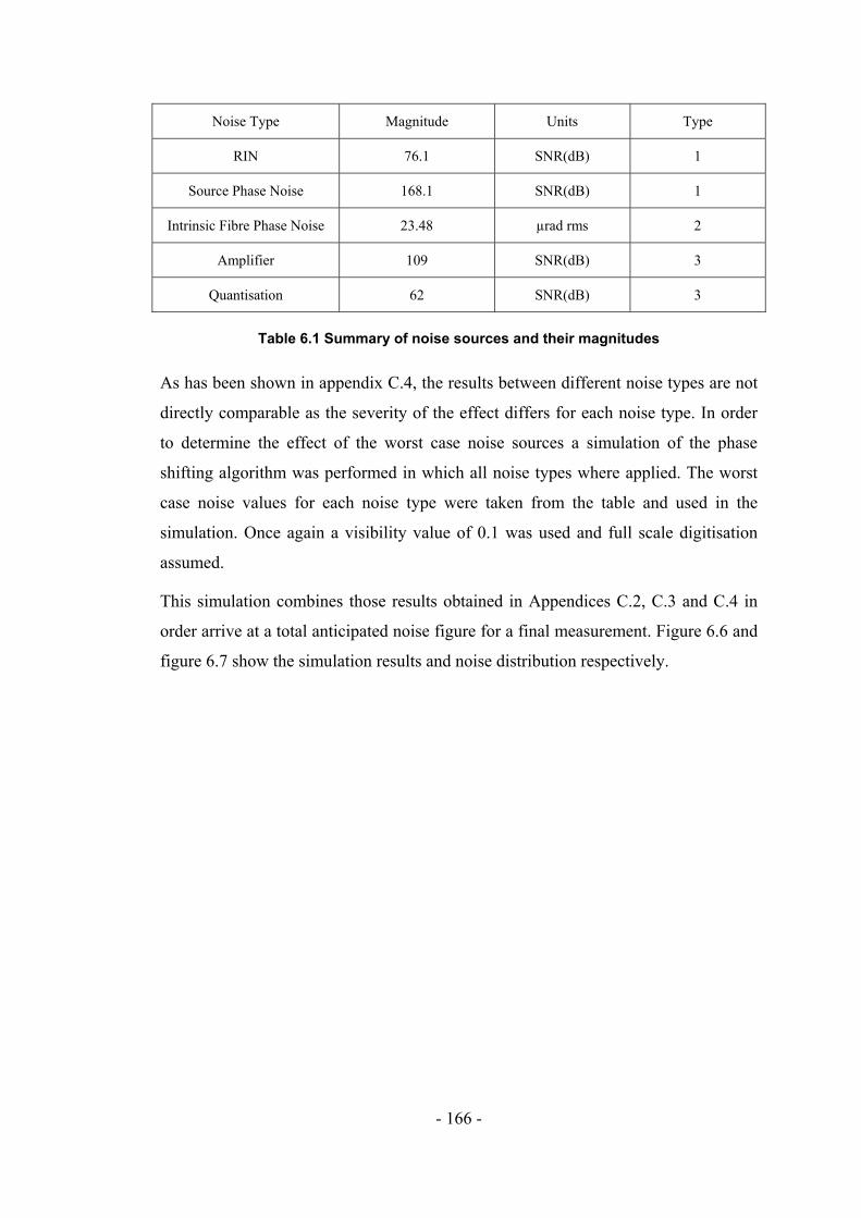
- 166 -
Noise Type Magnitude Units Type
RIN 76.1 SNR(dB) 1
Source Phase Noise 168.1 SNR(dB) 1
Intrinsic Fibre Phase Noise 23.48 µrad rms 2
Amplifier 109 SNR(dB) 3
Quantisation 62 SNR(dB) 3
Table 6.1 Summary of noise sources and their magnitudes
As has been shown in appendix C.4, the results between different noise types are not
directly comparable as the severity of the effect differs for each noise type. In order
to determine the effect of the worst case noise sources a simulation of the phase
shifting algorithm was performed in which all noise types where applied. The worst
case noise values for each noise type were taken from the table and used in the
simulation. Once again a visibility value of 0.1 was used and full scale digitisation
assumed.
This simulation combines those results obtained in Appendices C.2, C.3 and C.4 in
order arrive at a total anticipated noise figure for a final measurement. Figure 6.6 and
figure 6.7 show the simulation results and noise distribution respectively.

- 167 -
0 5000 100000
2
4
6
8Input Phase
Pha
se A
ngle
(rad
)
Sample Number0 5000 10000
0.8
1
1.2
1.4Fringe Intensities
Nor
mal
ised
Inte
nsity
Sample Number
0 5000 100000
2
4
6
8Calculated Phase
Sample Number
Pha
se A
ngle
(rad
)
0 5000 10000-5
0
5x 10⁻³ Error
Sample Number
Pha
se A
ngle
(rad
)
Figure 6.6 Estimated worst case noise on MFI from quantifiable noise sources
-5 -4 -3 -2 -1 0 1 2 3 4 5
x 10-3
0
0.1
0.2
0.3
0.4
0.5
0.6
0.7
0.8
0.9
1Output Noise
Nor
mal
ised
Fre
quen
cy
Phase (rad)
Figure 6.7 Output noise histogram
From the Gaussian distribution calculated rms value for the error is 0.006 rad. It is
thus possible to consider that the peak to peak noise will be approximately 0.036 rad.
This equates to a peak to peak error in the calculated height of 4.48 nm.
Bearing in mind that these are the theoretical minima and other unquantifiable effects
such as etaloning and SOP evolution are not included in this analysis meaning that in
reality this figure is most likely too generous. A rule of thumb is that the noise level

- 168 -
should be at the very most an order of magnitude lower than the required
measurement resolution. However from table 6.1 it is seen that the quantisation noise
is the limiting factor. Just increasing the resolution of the ADC converter to 16 bits
would raise they SNR to above that contributed by RIN. The NI PCI-6221 DAQ card
used in the first instrument for instance has an approximate SNR of 89 dB. This
would suggest a noise level of 0.0012 rad rms or 0.8637 nm peak to peak with the
device now being RIN noise limited.
One extremely important factor in the noise performance is the visibility of the output
fringes. Table 6.2 shows the peak to peak noise in nm for a range of different
visibilities for the RIN noise limited scenario discussed in the preceding paragraph.
Visibility Noise (nm pk-pk)
0.1 0.8951
0.2 0.4778
0.5 0.1841
0.9 0.1087
Table 6.2 Effect of fringe visibility on output noise
It can be seen from table 6.2 that increasing the visibility causes an equivalent
reduction in output noise. It is therefore vital that the visibility is kept to a maximum
at all times. During the experimental work it was found that a working visibility of
over 0.5 was easily maintainable.
6.5 Conclusion
The major sources of noise occurring in optical interferometers have been identified,
and where possible quantified. Simulation was used to analyse the effects of the
various noise types for a phase shifting interferometer. The Carré phase shifting
algorithm was shown to slightly reduce the effects of type 2 and 3 noise. Type 1
noise such as laser source RIN however was found to be amplified.
The results suggests that the inherent limitation in the sensitivity of the instrument to
make sub-nanometre measurement is currently RIN in the laser sources assuming all
other instabilities such as etalon effects, polarisation instability and environmental

- 169 -
disturbance can be reduced to a low enough level is the RIN noise. The figures
arrived at were purposefully conservative, all being worst case scenarios. For an
average fringe visibility of 0.5, a peak to peak noise figure of 0.184 nm was derived.
In order to reduce this any further it would be necessary to use RIN reducing
techniques. This is however more than an order of magnitude less given for peak to
peak repeatability of 3 nm given in the original specification in section 5.1. In
conclusion there is no theoretical reason why the pecification cannot be reached
provided that the instability caused by the SOP evolution is overcome.
The noise analysis in this chapter derives the minimum requirements for the
interferometer in order for it to meet the specification. The results explain the
limitations of the instrument described in chapter 5, which were determined to be
mainly due to polarisation instability. The same results will be taken forward and
used to explain the limitations concerning the instrument in chapter 7 which will be
seen to be mainly due to the ADC used.

- 170 -
7 Rapid Phase Shifting Interferometer
7.1 Introduction
The MFI described in chapter 5 was shown to have potential for surface profiling
using wavelength scanning and optical fibre. It suffered from several disadvantages
however. The active stabilisation scheme appeared to be somewhat ineffective at low
frequencies. The measurement interferometer exhibited a low frequency drift of 5.5
nm peak to peak which translated into a measurement repeatability of approximately
11 nm. This was shown in section 6.3 to be due to SOP evolution in the fibre which
causes fringe visibility variation. This means that there is not a stable intensity to
phase relationship and as such the stabilisation method is flawed at the low
frequencies over which SOP evolution occurs.
Clearly a more stable feedback parameter is necessary if the interferometer is to be
stabilised effectively enough for carrying out surface metrology. The ideal situation
would be to use the phase of the interferometer as the feedback quantity since this is
what we are trying to stabilise. This requires the use of phase shifting algorithms to
calculate it and in order to carry this out for use in a real time control loop it would
require an extremely fast phase shifting actuator.
The original specification as described in chapter 5 is shown below to recap.
Performance Target Value
Measurement Time < 60 s
Vertical Uncertainty <0.5 nm rms
Vertical Range > 0.5 µm
Lateral Resolution Diffraction Limited
Lateral Resolution Diffraction Limited
Table 7.1 Instrument specification
7.2 Rapid Phase Shifting Method
7.2.1 Overview

- 171 -
As mentioned in section 6.3 the fringe visibility and intensity variation arising from
SOP evolution and polarisation dependent components in the interferometer arms is a
relatively low frequency effect, with most of the energy being below 1 kHz. The
novel idea introduced here is to perform the phase shifting extremely quickly in order
to determine the phase before any significant movement of the operating point has
occurred due to environmental disturbance or SOP evolution. This would in effect
present a stable snapshot of the current phase of the interferometer. If the phase
shifting could be carried out at sufficient speed it would be possible to use the phase
as the feedback quantity by which to stabilise the interferometer. Figure 7.1 illustrates
the concept of a rapid phase shifting method.
A mechanical shifted mirror mounted on a PZT is far too slow to contemplate using
such a method. In addition the problems of non-linearities and hysteresis mean that
the attainable open loop accuracy might well be problematic for stable measurement.
What is required is a fast phase shifter that can supply open loop accuracy at very
high speeds. This possibility lies in the form of an EOPM (electro-optic phase
modulator).
Calculated Phase
Calculated Phase
EOPMV
Time
Calculated PhaseCalculated Phase
Calculated PhaseCalculated Phase
EOPMV
Time
EOPMV
Time
Figure 7.1 The rapid phase shifting concept
7.2.2 Electro-Optic Phase Modulator (EOPM)

- 172 -
An electro-optic modulator (EOPM) is capable of providing very rapid variation in its
refractive index when a strong electric field is applied across it. By placing an EOPM
in the arm of an interferometer it can be used to vary alter the phase in that arm as the
refractive index change in the crystal alters the optical path length. This has the same
effect as the PZT mounted mirror in the first scheme. However, there are no moving
parts involved and access times are much quicker. The variation of optical path
length by changing the refractive index over part of the geometric path results change
in the overall optical path.
There are two types of electro-optical effect; the Kerr effect and the Pockels effect.
The Kerr effect is a quadratic electro-optic effect in which the index change is
proportional to the square of the applied electric-field. The Pockels effect is a linear
electro-optic effect and in generally is much stronger than the Kerr effect. For this
reason it is much more commonly harnessed for the production of electrooptic
modulators. A Pockels cell acts as a variable wave plate and as such if placed
between crossed polarisers can be used as an intensity modulator. The other
application is as a phase modulator.
Lithium Niobate (LiNbO3) is a common crystalline material for Pockels cells as it
exhibits a strong effect and is transparent for wavelengths from 0.4 – 4.5 μm. The
electro-optic coefficient is found to be non zero only along certain crystal axes and as
such the orientation of the optical axis and the applied electric field through the
modulator is critical to its operation. Lithium niobate is naturally birefringent in the
absence of an applied electric field and its index ellipsoid is given by
2 2 2
2 2 2 1o o e
x y zn n n+ + = (7.1)
where on and en are the ordinary and extraordinary indices. If the optical axis is
aligned with the crystal z axis then any linear polarisation state is maintained. The
electro-optic coefficients in lithium niobate vary with orientation with the crystal
axes. In general it is preferable to align the direction of the applied electric fields with
the direction of the strongest coefficients in order to maximise the efficiency of the
device. The figure of merit for an electro-optic modulator is the half-wave voltage,

- 173 -
V Lπ product which is the voltage required to alter the phase by π radians multiplied
by the length of the device (Saleh & Teich 1991, ch. 12).
LiNO3 Crystal
Applied E-field
LinearPolariser
OutputLight
InputLight
LiNO3 Crystal
Applied E-field
LinearPolariser
OutputLight
InputLight
Figure 7.2 Operating principle of an electro-optic phase modulator
7.2.3 Bulk Electro-optic Phase Modulators
Traditional bulk optic EOMs are expensive to drive as they have large apertures and
thus large crystal thickness requiring very large voltage to be applied in order to set
up the required electric field. This is true of both transverse and longitudinal
modulators, although transverse modulators generally have a much lower V Lπ
product at the expense of polarisation dependent operation (New Focus 2009).
Typical values of Vπ for bulk optic EOMs are in the range of 300V at operating
wavelengths around 1500nm. Thus with a driver operating with a ±400V range, and
bearing in mind that any phase shift introduced in the arms of a Michelson
interferometer is effectively doubled, a total phase tracking range of roughly 5.2π
radians (4.16 μm actual displacement) is possible with commercially available
equipment. However, the electronic drivers are complex and expensive. Speeds are
also limited due a combination of very high slew rates, the voltages required and the
capacitive load the EOPM presents. A few such interferometric systems have been
developed already by Sandoz et al. (1999) as well as Zhao & Burge (2001).
7.2.4 Integrated Optics EOMs
Communications technology provides a cheaper and much improved solution that
may be integrated into a fibre optic interferometer to provide the same stabilisation
feature. Integrated optic phase modulators perform the same function as there bulk
counterparts, but due to the long length of the waveguide compared to its narrow
- 174 -
width, values of Vπ can be as low as 3V. They also present a small capacitive load,
typically a few picofarads, which means that the driving electronics can be relatively
simple for modulation speeds of a several MHz, although cutting edge design has
seen operation at a frequency of 100 GHz (Saleh & Teich). Generally the upper
frequency limit is defined by the capacitance of the modulator and the length of the
active waveguide structure. The reason for the latter is that the transition time of the
light wave must be short enough that the refractive is approximately constant during
its time in the waveguide.
The optical fibre based design of the MFI makes the use of an integrated-optic EOPM
an attractive proposition and suggests a good potential for implementing a fast phase
shifting technique for real time phase retrieval.
Figure 7.2 shows the structure of a typical EOPM. In order to make use of the
maximum electro-optic coefficient, it is normal for the crystal to be placed in the so
called x-cut orientation. This means the optical axis aligned with the y axis of the
crystal while the electric field is applied along the z axis. This results in the following
equations for degenerate polarisations states along the z and x axes.
3
332e
z e znn n r E= − (7.2)
3
132o
x o znn n r E= − (7.3)
The polarisation along the z and x crystal axes represents the TE and TM polarisation
states in the waveguide respectively. The electro-optic coefficients values are 12
33 30.9 10r −= × and 1213 9.6 10 m/Vr −= × . As such it is quite clear from 7.1 and 7.2
that the magnitude of the index change is different for the TE and TM polarisations.
The result is that a varying birefringence is created since the phase of the TE and TM
are altered unequally. Therefore in order for the EOPM work at its most efficient and
without altering the SOP of the light it is critical that the input light is aligned to the
TE axis. One approach to this is to install a linear polariser with a suitably aligned
active axis in front of the active waveguide element of the EOPM. This provides a
simple approach for use in single mode fibre coupling where the polarisation state is
unknown and varies with time. The disadvantage is the loss of some light power in

- 175 -
the arm of the interferometer containing the EOPM and the addition of added
intensity dependence on the SOP.
An EOSpace Inc. phase modulator was acquired for the experimental work presented
in this chapter. Its specification suggests a return loss of >50 dB and an insertion loss
of <10dB combined with a 4 VVπ < . The maximum operating voltage range is ±30
V which yields a total equivalent operating range of approximately 15 μm. It has a
capacitance of 80 pF.
7.2.5 Rapid Phase Shifting Method
In order to perform phase shifting with the EOPM all that is required is to apply a
staircase voltage waveform of sufficient accuracy. The output intensity of the
interferometer is then sampled after suitable settling time has been allowed. The
settling time requirement is due to the interaction of the driving electronics and the
intrinsic capacitance of the EOPM. It should not be confused with mechanical
settling time as might be experienced with the stepwise shifting of a PZT.
Initialise
Shift EOPM Phase
Wait for settle
Sample Intensity
Calculate Phase
Reset EOPM Phase to Initial Value
Output Calculated Interferometer Phase
N ti
mes
Figure 7.3 Flow of events during rapid phase shifting
In order to define stabilise the interferometer it is necessary to servo the phase in
opposition to the change induced by environmental factors. This is easily done during
the phase stepping process by simply altering an offset voltage on the output. This is

- 176 -
independent of the phase stepping and is simply added to the output. It may be
thought of as adjusting the DC offset of the phase stepping waveform.
In order to use the modulator effectively as an open loop phase shifter, it is necessary
to characterise exactly the response of the modulator to an input voltage. In order to
do this the EOPM was placed in the arm of an all fibre Mach-Zehnder Interferometer
and modulated with a triangular waveform with a frequency of 20 kHz. The
amplitude of the modulating wave form was such that it created just over a full fringe
phase shift. The fast modulation frequency ensures the results are not distorted by any
low frequency environmental disturbance.
Figure 7.4 shows the output of the interferometer (red trace) and the modulating
voltage waveform (black trace). The sinusoidal intensity response to the linearly
ramped phase input is quite apparent. The operating wavelength was 1550 nm.
Figure 7.4 Calibration of Vπ for an EOPM
From figure 7.4 it is clear that the modulation voltage required to produce one full
fringe is 3.86 volts. Bearing in mind that a Michelson interferometer apparatus,
which the EOPM will ultimately be used in, has double the phase shift of a Mach-
Zehnder the conversion gain is,
4 rad/V3.86 0.965EOMK π π= = (7.4)
This equates to a voltage step of 0.483 V to create a 90.0° phase shift.
7.3 Experimental Setup

- 177 -
7.3.1 Apparatus
12
3
Tune
able
Las
er
Sou
rce
Lase
r Dio
de
12 b
it A/
D
PSI
Algo
rithm
4 W
ord
Buffe
r PC
12
3
λ r
λ m
REFMirror
Diff
ract
ion
Gra
ting
Col
limat
ing
Lens Su
rface
PIN
Det
ecto
rPI
ND
etec
tor
Circ
ulat
or A
Circ
ulat
or B
FBG
3dB
Cou
pler
A
λ mλ r
λ rλ mλ m
+λ r
λ m +λ r
λ m +λ r
TMS3
20F2
812
DSP
3dB
Cou
pler
B
GR
INLe
ns
GR
IN L
ens
16 b
it D
/API
D
Algo
rithm
Step
W
avef
orm
Gen
erat
orSP
I In
terfa
cex3
±12V
+
8 Sa
mpl
e Av
erag
e
12 b
it A/
D8
Sam
ple
Aver
age
4 W
ord
Buffe
r50
0 W
ord
Buffe
r
Para
llel
Inte
rface
GPI
BIn
terfa
ce
EOM
Driv
er B
oard
x50k
x50k
Buffe
r
Buffe
r
Tran
sim
peda
nce
Ampl
ifier
Boa
rd
Opt
ical
Pro
be
EOM
Mea
sure
men
tR
efer
ence
Com
bine
d
Figure 7.5 Experimental Setup
Many of the features of the experimental setup in this chapter are identical to those
contained in the instrument described in the chapter 5. As such the reader is referred
to section 5.3 for detail on those features which are common to both instruments.

- 178 -
The experimental setup investigated in this chapter is shown in figure 7.5. A laser
diode and the tuneable laser (Hewlett Packard 6181F) illuminate the reference and
measurement interferometers respectively. This tuneable laser source replaced the
Ando AQ4320D that was used in the setup in chapter 5, the reason being an
irreparable malfunction.
The laser diode operates at a wavelength of 1550nm and the TLS is operated between
1555 nm and 1575 nm. Both sources are multiplexed into the same fibre by a 3dB
coupler, which is followed by a circulator to provide isolation. A second coupler then
splits the light into two fibres, which form the arms of a Michelson interferometer.
The polarisation state of the input light is adjusted using a Lefevre type polarization
controller (see section 6.3.4). The polarisation controller is somewhat limited in that
it cannot maximise the polarisation state of both light sources at the same time, a
separate controllers at the output of each source would be required for that. It does
however allow a rough adjustment to gain good fringe visibility in order to maximise
SNR. Once this coarse adjustment is made it maintains a good degree of stability for
several minutes.
7.3.2 Optical Probe
A key difference in this scheme when compared to the setup in chapter 5 is in the
design of the optical probe. The main difference is the lack of a reference mirror; in
fact the zero order is not utilised at all. The first order beam is diffracted as before,
and the sweep angle altered by wavelength tuning as described in section 5.4.2. The
analysis for the scanned profile length is similar but with differing parameters due to
a different objective lens.
The objective lens use in this setup is the Thorlabs LSM-03 object telecentric
scanning lens. It is specifically designed for optical coherence tomography (OCT)
applications where by a light beam is scanned very quickly over the lens aperture
whereby it is focussed upon the objective surface. This is a very similar action to the
one carried out in this instrument and as such provides performance advantages for
this system in terms of spot size when compared to the basic achromatic doublet as
used in chapter 5.

- 179 -
The effective focal local of the LSM-03 lens is 35.98 mm, and with a 4 mm
collimated gaussian beam at the aperture it will provide a focussed 25 μm spot size
with a 580 μm depth of field. The maximum scanning range is limited by the field of
view of 9.4 mm.
Approximate Linear Dispersion with Wavelength
-2
-1.5
-1
-0.5
0
0.5
1
1.5
2
1555 1556.9 1558.8 1560.8 1562.7 1564.6 1566.5 1568.4 1570.3 1572.3 1574.2 1576.1 1578
Wavelength (nm)
Line
ar D
ispe
rsio
n (m
m)
Figure 7.6 Optical probe scanning profile
A numerical analysis similar to that carried out in section 5.4.2 was carried out with
the grating incidence, 26α = ° . It can be seen that the scan range is approximately 3.2
mm. The wavelength scanning range is slightly reduced from that used in section
5.4.2 because of the slightly reduced wavelength scanning range of the HP8168F
tuneable laser; the output intensity was found to drop off rapidly above 1578 nm.
It is likely that the current configuration the produced spot size is not optimal as the
collimated 21/ e beam width supplied by the collimating GRIN lens is only 0.85 mm
rather than the specified 4mm. Further beam expansion optics would be required
between the GRIN lens and the grating.
Overall the probe created for this apparatus is much smaller than that of the
instrument in chapter 5 due to the fact there is no reference arm contained within the
bulk optic element. The probe head form factor is reduced from 70 x 100 mm to
approximately 70 x 30 mm.
7.3.3 Reference Arm

- 180 -
The reference arm of the interferometer is now formed in fibre by the second coupler
output. It contains the EOPM which is used to stabilise the interferometer and
perform phase shifting. The integrated optic EOPM comes fibre pigtailed so
connection to the optical circuit is a simple matter.
Because there is EOPM has a relatively limited range (≈15 µm) it is necessary to pass
the light through a GRIN lens so it may be incident on an external reference mirror.
This is less efficient than directly silvering the fibre end but allows the mounting of
the mirror on a translation stage. This method means the interferometer is easily
balanced manually, until it lies in the EOPM operating range. This type of adjustment
would be necessary if the objective lens was to be changed to one of a different
magnification for instance; the path length in the measurement arm would then
change substantially. If fully automated operation was deemed to be necessary, the
translation stage could be easily be motorised.
7.3.4 Electronic Hardware
One of the largest differences between the instrument described in chapter 5 and this
one is in added electronic hardware needed to implement the rapid phase shifting
technique. This section gives an overview of the electronic elements of the apparatus
and explains their function and inter-relationship.
A functional representation of the hardware is given in figure 7.7.
Figure 7.7 Functional representation

- 181 -
The diagram is divided in physical terms with each of the large boxes representing a
different physical printed circuit board (PCB). The PCBs contain a number of sub-
circuits which are represented inside the main boxes. The full circuit diagrams for
each of the sub-circuits are contained in appendix B. The arrows on the diagram
indicate the direction of dataflow. Software is represented by the dashed boxes. A full
diagram, included pinouts relating to the subcircuit diagrams in Appendix B.1 to B.3
may be found in Appendix B.4
Transimpedance Amplifier
The fast phase shifting requires a transimpedance amplifier with fast frequency
response since this translates directly to rise times. With this in mind the THS4062
opamps were used since they provide a very high GBW and fast response. A full
noise analysis is carried in appendix A.2. There are two transimpedance amplifiers,
for the reference and measurement interferometer outputs respectively. They are two
stage amplifiers which allows for high speed and gain adjustment in order to
condition the signal for full scale analogue to digital conversion. The outputs from
both transimpedance amplifiers are fed to the ADC on board the TMS320F2812
PCB.
Auxiliary Board
The auxiliary board contains several logic level translators to isolate the sensitive 3.3
V CMOS inputs of the DSP and convert from the TTL levels used by the PCI-6221
DAQ card. It also provides for the reverse conversion for the DSP outputs as
necessary.
The EOPM driver provides a gain of 3 to amplify the output of the DAC (±3 V) into
a larger value in order to provide for a larger range of operation. The THS4062
opamp also provides a high frequency response to ensure the system bandwidth is not
limited here.
The response of the EOPM driver and the transimpedance amplifier during phase
stepping is shown in figure 7.8.

- 182 -
Figure 7.8 Response of MFI to phase shifting
It is quite clear that the EOPM voltage has a much faster rise time than the response
of the transimpedance amplifier. The transimpedance response is seen to be critically
damped in order to ensure a fast settling time for sampling. This was done by
adjusting the feedback capacitance of the amplifier (see appendix A.1). Figure 7.9
shows more clearly the voltage across the EOPM (red trace) from an input (green
trace). The 34 ns rise times equates to an approximate bandwidth of 10 MHz
assuming a first order approximation for the response.
Figure 7.9 Response of EOPM voltage to an input square wave
TMS320F2812 Digital Signal Processor
In order to provide real time phase calculation for the interferometer at a speed fast
enough be used in a servo control loop a digital signal processor (DSP) is very

- 183 -
suitable. It benefits from being deterministic in operation, something that is difficult
to obtain on a PC loaded with a modern day operating system. The TMS320F2812 is
a fairly cheap processor which still provides 32 bit fixed point processing at 150
MIPS as well as 18 k (16 bit words) of onboard mixed use memory (programs or
data). In addition it hosts a number of onboard peripherals, the most relevant to this
application being the ADC, serial peripheral interface (SPI) and the configurable
general purpose inputs/outputs (GPIO).
The DSP is connected to a PC by a parallel interface and built in JTAG module. This
allows the downloading of program code and the upload of stored data from the DSP
and provides in-circuit software debugging. Texas Instruments Code Composer
software provides an integrated development environment (IDE) with includes a
C/C++ compiler and debugger. In addition a set of functions is provided for carrying
floating point arithmetic and trigonometric functions on the fixed point architecture.
The ADC is has 12 bit resolution and features a multiplexed input so up to 16 inputs
may be sampled, though overall sample rate is shared between them. The input signal
range is 0-3.3 V and as such the transimpedance signals must be conditioned
correctly. Maximum sample rate is 12.5 MSPS. The ADC is used in simultaneous
sample mode where two inputs are sampled simultaneously; A0 and B0 which are
connected to the reference and measurement interferometer outputs respectively.
The SPI is a 4 wire bi-directional synchronous serial interface, the clock being
provided by the DSP. For this application it is used in a uni-directional mode (3 wire)
to supply 16 bit values to the DAC which provides the analogue voltage signal to the
EOPM. The maximum bit rate of the SPI is 12.5 Mb/s which means the maximum
update rate is approximately 735 kHz (16 + 1 bits/sample). This equates to a 1.36 µs
delay between DAC updates.
The GPIO interface provides configurable digital input and output. Two ports are set
up to provide a simple means of synchronising with the Labview code running on the
PC for the task of changing the laser wavelength. In addition to this some outputs are
provided for flagging/debugging and timing analysis.
Interface Board

- 184 -
The interface board provides three functions. It has logic level translators to convert
the 3.3 V CMOS outputs from the DSP to power LEDs for signalling. It also has 3
TTL to 3.3 V CMOS converters to allow for protected digital signalling to the GPIO
inputs on the DSP.
The most important function of the interface is the AD766JN DAC which provides
the analogue output for driving the EOPM. It is connected to the DSP by a 3 wire
uni-directional SPI and accepts data in 16 bit words at a rate of up to 12.5 Mb/s. The
AD766JN DAC has a 16 bit resolution and a worse case settling time of 1.5 µs after a
data value change. Combined with the 1.76 µs delay caused by the transfer time of
the SPI the overall delay time is 2.86 µs; this means a real world maximum update
rate 350 kHz.
PC
The PC performs several functions and runs two software applications, Labview and
Code Composer. The Labview software liaises with the PCI-6221 DAQ card and the
GPIB interface. The Labview code performs the post-processing duties on retrieved
data from the DSP after a measurement has taken place. It also controls the HP8168F
tuneable laser via the GPIB interface. The Code Composer software is dormant
during the measurement cycle, its only function is to upload that measurement data
from the DSP for post-process once the measurement is finished.
Laser Diode Driver
The laser diode driver is based around a specialised laser diode driving IC. It
provides a quiet constant current source, and uses feedback from the monitor
photodiode integrated in the laser diode to provide feedback for intensity control.
There is a modulation input provided which may be used to modulate the injection
current at frequencies a few kHz by the simple application of voltage waveform. This
is a useful function which aids optical path length balancing prior to measurement.
7.3.5 Software
DSP Code Overview

- 185 -
TMS320F2812 DSP
12 bit A/D
PSI Algorithm
4 Word Buffer
PC
PID Algorithm
Step WaveformGenerator
SPI Interface+
8 Sample Average
12 bit A/D
8 Sample Average
5000 Word Buffer
ParallelInterface
DAC
Measurement Interferometer
ReferenceInterferometer
Figure 7.10 DSP code function diagram
Figure 7.10 shows the functions of the DSP code in terms of task modules. First the
intensity data from both the reference and measurement interferometer are sampled 8
eight times in 80 ns intervals. The sample values are then averaged in an attempt to
lower noise slightly. The reason for the choice 8 values is that this is the maximum
buffer size on the ADC module and division by eight is quickly achieved in binary
processing by right shifting the register value by 3 bits.
The 8 averaged sample value is then stored in a buffer and the SPI outputs the next
phase shift value. After a delay of 2.86 µs in order to allow the DAC to update and
settle the sampling process is repeated.
The phase shift sampling is carried out 4 or 5 times depending whether the Carré or
Schwider/Hariharan algorithms, respectively, are selected for calculating the phase.
The step voltage values are supplied by the step waveform generator which is a
simple circular buffer containing the required voltage value.
The PSI algorithm themselves are coded using the supplied IQmath C functions that
allow for emulation of floating point arithmetic and trigonometric functions with
maximum efficiency. This important because the phase calculation is the most
significant single delay in the servo loop. Figure 7.11 shows the voltage applied to

- 186 -
the EOPM during the phase shifting process, the total time for phase calculation
using the Schwider-Hariharan is approximately 27 µs.
Figure 7.11 Diagram of Schwider-Hariharan phase shifting method
The Carré algorithm only requires 4 phase shifts which should save 2.86 µs over the
Schwider-Hariharan but in reality the square root in the numerator removes this
advantage. Evaluation of this take 63 clock cycles (5.04 µs) and in addition the
conditions testing for the arctangent quadrant determination is more complex (see
section 5.5.3). The relatively simple Schwider-Hariharan, when evaluated at a 90°
phase shift, works out to be substantially faster.
After the phase is calculated it is used to update the PI control algorithm. Because of
the digitisation of the phase signal it makes good sense to use a discrete control
algorithm on the DSP, since it is easily configurable and convenient. It imparts a
minimal delay due to its simple nature, being only effectively a recursive 3 tap filter.
The output from the control algorithm is added to the step voltage value
Samples captured from the measured interferometer synchronously with those from
the reference interferometer. However, in order to maximise the loop rate, the phase
is not evaluated and the raw intensity values are simply stored in memory. Add the
end of the measurement cycle the intensity data is uploaded to the PC via the parallel
interface after which the phase is evaluated using Labview code.
Labview Code Overview

- 187 -
In comparison to the Labview code for the MFI in chapter 5 the requirements in this
instrument are relatively little. This is in the main because the majority of the actions
are performed on the DSP.
The Labview code simply communicates with the HP8168F laser during the
measurement cycle, via the GPIB interface, and commands it to shift wavelength as
necessary. It also post-processes the upload measurement intensity data from the DSP
to provide the final profile data. A full run down of the functions is given in appendix
F.
7.3.6 General Points
The wavelength de-multiplexing method remains the same as the MFI described in
chapter 5. The main difference in the optical setup is that this is now an all-fibre
interferometer in the sense that the interference of the returning waves in each of the
interferometer arms now takes place at the coupler. This is an importance difference
compared to the instrument in chapter 5 which was essentially a bulk optic
interferometer where the arms were in free space. The all-fibre nature of the
apparatus described here is such that it is substantially less stable and much more
sensitive to vibration and temperature change. Clearly this places more of a challenge
for the servo control loop.
Onboard memory limitations mean that the buffers for storing the calculated
reference phase values and the raw measurement intensity data are limited to 1000
and 5000 (16 bit words) respectively. The larger allocation for the measurement data
it is necessary because of it is unprocessed until the end of the measurement cycle.
The algorithm used to calculate the phase feedback signal may be selected as the
Carré algorithm (4 phase shifts) or the Schwider-Hariharan (5 phase shifts).
7.3.7 Balancing the Optical Paths
In order to balance the optical paths a simple procedure is carried out in which the
wavelength of the laser diode is modulated. This is done by altering the injection
current by applying a voltage waveform to the mod in input on the laser diode driver
(see appendix B.3). The DSP code is run and it proceeds to lock the interferometer
stable. The modulation of the injection current causes a shift in intensity and in

- 188 -
addition a small variation in wavelength. This is due mainly to the associated
temperature change in the cavity due to changing injection current modulation. For
an unbalanced interferometer, any wavelength modulation will result in a modulation
of the output phase. As such this modulation is servoed against by the closed loop
control.
By monitoring the measurement interferometer output waveform, which looks similar
to that shown in figure 7.8, it is possible to see the servoing of the control loop as a
shift in the positions of the observed steps. The rapid phase shifting techniques
overcomes any problems with the change in fringe intensity that results in by
modulating the laser diode intensity as long as the level does not drop too low.
By modulating the laser diode slowly at 0.5 Hz and observing the output of the
measurement interferometer the reference mirror is translated on a micrometer stage
until the stepped intensity waveform is completely stable. At this point the optical
paths of the interferometer are balanced and the measurement may proceed.
7.3.8 The Measurement Cycle
A full transcript of the DSP and Labview code is given in appendices D and E2,
however it is worth describing the operation in terms of event flow in order to
maintain clarity.

- 189 -
Initialise Laser
Initialise DSP Peripherals
Sample intensities
Read next phase shift value
Request laser wavelength step
Upload measurement intensity data
Add to EOPM voltage
Wait for EOPM settle
Run PSI algorithm
Run control algorithm
Store intensitiesMeasurement
intensities stored?
Update EOPM voltage
End
All measurement
points complete?
Wait for laser settle
No
Yes
Yes
No
Wait for laser move complete
Figure 7.12 Event flow during measurement cycle
First the tunable laser is initialised and the wavelength is set at 1555 nm to place the
measurement point at the start of the profile. During this time the DSP code is
downloaded on the DSP and started up. This runs several routines for setting up the
onboard peripherals with the required parameters for correct operation. Ones these
have been set up the DSP runs in phase shifting mode.
It is important to note that the phase shifting, evaluation and control algorithms run
continuously during the whole of the measurement cycle, regardless of what position
in the event flow the rest of the code is. This is achieved by using the hardware
interrupt and an associated interrupt service routine (ISR) which automatically runs at
specified intervals regardless of the current position in the overall program. The
interrupt utilised is the ADC conversion complete interrupt; this is called every time a
conversion is complete. In this way the code automatically jumps into the routine

- 190 -
every time the intensity has been sampled and deals with the sample accordingly. The
ADC conversion complete ISR is shown on the event flow diagram as a yellow
square. By using an interrupt driven control loop in this way, the timings are
deterministic, with a total control delay of 27µs.
There is only one occasion when the DSP needs to communicate with the Labview
code and that is to request for the laser wavelength to be shifted to the next point on
the profile. The actual step values are help in an array in Labview and are user
configurable. To do this the DSP logic pin PWM11 high which is detected by DAQ
card on pin 0.0. The Labview code then issues a command, via the GPIB interface, to
set the laser to the next wavelength step and waits for a service request (SRQ) from
the laser which signifies the wavelength shift has completed. The DAQ card pin 0.1
is then set to logic high to inform the DSP code that the laser shift has completed; this
is picked up by DSP pin PWM10 (see figure 7.7). The DSP then pulls PWM11 low to
acknowledge and the interface returns to an original state. Figure 7.13 shows a timing
diagram describing this procedure.
PWM10
P0.1
RequestMove
MoveComplete
ACK ACK
L
L
H
H
L
L
Time
LogicLevel
Figure 7.13 Laser move request timing diagram
There are various parameters that may be altered in the code for such things as
algorithm selection, control loop gains, phase stepping values and various delay
times. However, the full code listing and explanation of the parameters is given
appendix E.
7.3.9 Rapid Phase Shifting Operation

- 191 -
Figure 7.14 shows an oscilloscope trace of the rapid phase shifting method using the
Carré. The right hand side figure is simply a zoomed in version of the left hand side.
The black trace shows the interferometer output while the green trace shoes the
voltage applied to the EOPM. The red trace is a timing flag; the trace is high
whenever the DSP is calculating phase
Figure 7.14 Oscilloscope trace showing rapid phase shifting with Carré algorithm
Figure 7.15 again shows an oscilloscope trace of the rapid phase shifting method, this
time using the Schwider-Hariharan algorithm. This time the red trace shows the
interferometer output while the black trace shoes the voltage applied to the EOPM,
while the green trace is the timing flag.
Figure 7.15 Oscilloscope trace showing rapid phase shifting with the Schwider-Hariharan algorithm

- 192 -
The small transients seen on the EOPM voltage and interferometer output occur
during the write cycle for the DAC, there is some crosstalk or feed forward occurring.
It does not effect the accuracy of the phase shifting however because the sampling
does not occur until 1.5 μs after the DAC write has finished. This delay is to allow
the DAC to settle to within its specification. The extended time required at the end of
each 5 step phase shift sequence in order to execute the phase shifting algorithm is
quite clear.
7.4 Control Loop Analysis
7.4.1 Introduction
The control loop analysis given in section 5.4.4 anticipated how the stabilised
reference interferometer would respond to the any induced disturbance. In this
section a similar analysis is carried out for the fast phase shifting method. There are
three important distinctions between this method and the one convered in chapter 5.
The control loop is now digitally implemented, the dynamic of the phase modulator
are substantially different to that of the PZT and finally, the feedback parameter is
now calculated phase.
As such it is to be expected that the control loop behaviour may be substantially
different.
7.4.2 Block Diagram
In order to implement a suitable control loop one must first consider the
representation of the all the elements in the control loop. Figure 7.16 shows the
representation of an intensity feedback control loop. ( )U s being the target intensity
and ( )Y s the actual interferometer output intensity. EOMG , IFG and PING represent
the transfer functions of the EOPM, interferometer and the detector, while ( )C s is
some controller that we shall use to stabilise the system.

- 193 -
Figure 7.16 Representation of control loop
To simplify the analysis and convert to a phase based approach it is possible to make
some simplifications. First consider the effect of the phase shifting algorithm in a
control loop; it is not necessary to be concerned with the details of its workings from
the point of view of analyzing its effect on the control loop, it may be considered as a
‘black box’ which takes an input phase demand and delivers an output phase.
The action of the PSI algorithm is not continuous however, but discrete, providing a
phase output value every 27 μs after the code has run. As such, it is better consider
the loop as a z-domain representation having a sampling interval of 27 μs. The z-
domain is the discrete time equivalent of the s-domain representation and shares
many of its properties (Leigh 1985, ch. 2).
The upper half of figure 7.16 shows the full control loop in terms of s-domain
transfer functions. The lower half shows the simplified version in terms of z-domain
transfer functions.
7.4.3 z-domain Analysis
The z-domain transfer functions for a proportional-integral (PI) controller, ( )C z and
the phase shifting algorithm, ( )G z are
1( )G z z−= (7.5)
( )( ) 11p
i
TzC z KK z
⎡ ⎤= +⎢ ⎥−⎣ ⎦
(7.6)
T is the sampling interval and pK and iK are the controller gain and integration
time respectively. The forward loop transfer function is then simply;

- 194 -
( )
2
1 1( ) ( ) i
TK
c
zC z G z K
z z+ −
⋅ =−
(7.7)
From section 5.4.3, the sensitivity transfer function is then
( ) ( ) ( )
( )1
DG
G zSC z G z G z
=+
(7.8)
where the disturbance ( )D z enters at the point in the loop between ( )C z and ( )G z
on figure 7.16 The process for the discretisation of a continuous time PI controller is
given in appendix A.3.
7.4.4 Numerical Simulation
At this point numerical simulation was used to derive suitable values for PK and iK
in order to supply a stable closed loop and reasonable performance. This was done in
much the same manner as for the instrument in chapter 5. The script used may be
found in appendix D.5.
0 0.5 1 1.5 2 2.5 3
x 10-3
0
0.2
0.4
0.6
0.8
1
Kp=0.3
Time (sec)
Am
plitu
de
Ki=10 usKi=20 usKi=27 usKi=100 usKi=200 us
Figure 7.17 Simulated closed loop step response

- 195 -
Figure 7.17 shows the step response for various values of integration period (the
reciprocal of integration gain). The proportional gain was held steady at 0.3
throughout the simulation and the discrete nature of the output is quite clear.
Increasing the integration gain results in a faster response, up until a certain point
after which closed loop instability occurs. A critically damped response is apparent
when the integration period is equal to the PSI algorithm delay.
-100
-50
0
50
Mag
nitu
de (d
B)
100 101 102 103 104 105-180
-90
0
90
Pha
se (d
eg)
Ki=10 usKi=20 usKi=27 usKi=100 usKi=200 us
Figure 7.18 Bode plot of sensitivity function
Figure 7.18 shows a bode plot taken from the Matlab simulation. For 20 μsiK = and
0.3pK = it suggests that the -3dB point for disturbance rejection will occur at
approximately 1.6 kHz. As expected increasing the integration gain (reducing the
integration period) will improve the disturbance rejection up to the point of closed
loop instability.
It is clear that the main factor affecting the ability to upper frequency response of the
stable closed loop is the sampling interval of the loop enforced by the algorithm
execution time. The imposed sampling interval could be increased by a faster DSP

- 196 -
and by using a parallel loading DAC with a faster settling time, thus reducing the
wait time between phase shifts.
7.5 Experimental Results
7.5.1 Introduction
A similar set of experiments were carried out on this instrument in order to assess its
performance and compare it to the instrument in chapter 5. First, the stability of the
reference interferometer is measured, with the control enabled and disabled. The
effectiveness of the control loop is analysed with both the Carré and Schwider-
Hariharan algorithms used to calculate the realtime phase data. The SOP drift is then
measured to demonstrate the effect on long term stability. The stability of the
reference interferometer is then studied in detail over a shorter period of 10 seconds.
The measurement interferometer stability is also examined over the same period and
also at several different wavelengths. Finally, a step height sample is measured with
the MFI and also a Taylor Hobson CCI to provide a comparsion with a commercial
instrument.
7.5.2 Stabilised Reference Interferometer
In order to test the effectiveness of the phase feedback method for stabilising the
interferometer a variety of experiments were devised. First, the interferometer was set
free running with the stabilization control loop switched off, and the reference
interferometer output was monitored during this time. The control loop was then
enabled and once again the reference interferometer output was monitored. The
duration of monitoring was 2 seconds and the data sampling rate was 100 Hz; the
results are shown in figure 7.19. The results have been converted from phase to
nanometres of optical path change.

- 197 -
Figure 7.19 Drift seen in the stabilised/free running fibre interferometer
It is obvious that the drift when the interferometer is free running is severe and would
certainly impinge substantially on any real measurement attempted. The reference
interferometer output appears to be much improved when locked with the control
loop.
7.5.3 Short Term Reference Interferometer Stability
Figure 7.20, figure 7.21 and figure 7.22 show the reference interferometer calculated
phase output buffer. They represent the unlocked interferometer, a locked
interferometer using the Carré algorithm, and a locked interferometer using the
Schwider-Hariharan algorithm respectively. The sample rate was the maximum rate
for phase calculation at 37 kHz which equates to a 27 ms period for the 1000 phase
values recorded. The output phase values from the buffer are in radians.

- 198 -
Figure 7.20 Unstabilised reference interferometer with using the laser diode source1
Figure 7.21 Stabilised output using Carré algorithm1

- 199 -
Figure 7.22 Stabilised output using Schwider-Hariharan1
It should be noted that the scale in figure 7.20 is 20 times larger than that of figures
figure 7.21 and figure 7.22. Besides the obvious improvement in the stability over
that of the unlocked interferometer, it is also noticeable that there is significant
reduction in the noise present using the Schwider-Hariharan compared with the Carré
algorithm.
7.5.4 SOP Variation in the Stabilised Measurement Interferometer
Figure 7.23 shows raw captured intensity data from the measurement interferometer
with the active stabilisation switched on. The data were sampled at 100 Hz for an 8
second period. These are the raw intensity data that are post processed in Labview in
order to produce the measurement phase. Each coloured line represents an intensity
1 The y-axis in figure 7.20-23 represents calculated phase. Note the difference in scales between
figures 7.20 and 7.21 compared with 7.22. The x-axis shows the sample number.

- 200 -
set from a different phase shifted position. It is clear that although the interferometer
is locked, the intensities are varying due to SOP variation in the fibre. The drift seen
in figure 7.23 shows clearly why intensity feedback is not very effective for
stabilising fibre interferometers.
Figure 7.23 Drift of captured intensity values due to SOP variation
7.5.5 Reference Interferometer Stability Histogram
In order to ascertain the behaviour of the reference interferometer and to develop an
expectation of performance a detailed look at the statistics of the recorded positions
was made. 1000 consecutive reading of the calculated reference interferometer phase
where taken with the active stabilisation turned on. The results are shown in figure
7.24 in histogram format. The sample rate was 100 Hz thus the observation period
was 10 seconds.

- 201 -
Figure 7.24 Histogram of stabilized interferometer values
As might be expected there is an approximately normal distribution of values with a
standard deviation of 2.98 nm. It may be expressed from this result that
approximately ±9 nm range of stability has been achieved over 3 standard deviations
from the mean.
7.5.6 Stabilised Measurement Interferometer
While the preceding results show that the control loop effectively stabilises the
reference interferometer it is more important to concern ourselves with the stability of
the measurement interferometer. It is here that any variance of this phase that will
map directly onto the measurement result.
900 readings (imposed by DSP memory constraints) of the measurement
interferometer were taken at a particular wavelength with the interferometer locked.
In essence, the experiment made multiple measurements of the same point on the
measurand surface. The procedure was repeated at several wavelengths to see if there
was any variation over the effectiveness of the stabilisation over the whole scan
range. The sample rate was 100 Hz, thus the experiment covered an observation
period of 9 seconds.
Measurements were taken at 1560, 1565, 1570, and 1575 nm and the resulting spread
of surface height values at each operating wavelength are shown in histogram format
in figure 7.25.

- 202 -
Figure 7.25 Histograms of stabilised measurement interferometer at various tunable laser wavelengths
7.5.7 Step Height Measurement
The next stage of the analysis was to determine the abolsute accuracy of the
instrument within the bounds of its noise performance. In order to do this it is
necessary to perform a measurement of a known artefact; the same step height as was
used in section 5.6.6. In this experiment a different section (chrome coated) was used
however.
Figure 7.26 shows an areal representation the step height sample as captured using a
commercial scanning white light interferometer (Taylor Hobson CCI). The sample
was cold chrome coated to ensure equivalent optical properties for both the CCI and
our instrument especially with regard to phase change on reflection, thus ensuring the
results are directly comparable. A photograph of the sample is shown in figure 5.29.

- 203 -
Figure 7.26 Step height sample measured using Taylor Hobson CCI
Analysis of the step height shown in figure 7.26 suggests a step of 287 nm is present.
The angle of incidence on the diffraction grating in the MFI was setup to yield
approximately 2.5 mm of lateral scanning as the wavelength range was tuned from
1555 to 1575 nm. This ensured that the profile length was comparable to that
produced by the Taylor Hobson CCI which had a 3.68 mm2 field of view with the
lens used; the CCI results were cropped to match up the profile lengths.
Figure 7.27 Step sample profile as determined experimentally using a Taylor Hobson CCI
The total measurement time was about 120 seconds, this being due to tunable laser
used having a stepwise scan and requiring a long settling time of 0.5 seconds for a
stable intensity to be obtained after each step. Each data point was averaged 4 times
and figure 7.28 shows the acquired data using the MFI.

- 204 -
20 nm
Figure 7.28 Step Height as measured using the fibre interferometer
A peak to peak uncertainity of approximately 20 nm is clearly present on the
measurement result.
7.6 Discussion
7.6.1 Stabilised Reference Interferometer
The results for the unstabilised interferometer in section 7.5.1 are clearly quite severe
and the qualitative improvement with the active stabilisation is enabled is stark. This
is a good indication that the control loop is acting correctly.
Figure 7.19 suggests that the environmental drift is much worse than that experienced
by the instrument in chapter 5. The laboratory conditions were identical in both
situations, but figure 5.22 in chapter 5 shows much less drift on that instrument. This
was anticipated as the fibre arms are virtually all fibre and as such would be expected
to exhibit substantial optical path length change with environmental perturbation.
There is also another polarising element in the reference arm, the linear polariser in
the EOPM, which cause intensity variation in that arm. This is in addition to the
polarisation dependency of the diffraction grating already present in the measurement
arm.
7.6.2 Short Term Reference Interferometer Stability
The difference in the stability results between using the Schwider-Hariharan and the
Carré algorithms is of some interest. The results are substantially better with the

- 205 -
Schwider-Hariharan which is apparently at odds with the slower loop rate it produces
due to the 5 steps it uses which adds approximately 1.5 µs to the phase calculation
period. This is somewhat offset by the longer execution time required by the Carré
algorithm. This is in the main due to the square root in the numerator and the more
complex arctangent unwrapping routine; as such similar performance might expected.
One explanation could be due to the fact that the numerator in the Carré algorithm
can become imaginary due to noise. This results in a zero being evaluated by the DSP
and would then feed into the control algorithm with a resulting transient being
applied to the EOPM.
7.6.3 SOP Variation in the Stabilised Measurement Interferometer
The results show very clearly the problem that SOP variation causes in the fringe
visibility and certainly explains why there was low frequency drift present with the
intensity based feedback used in chapter 5. Figure 7.23 clearly show large drift of the
raw intensity values captured, even though the system is phase feedback stabilisation
is active. The fact that all four intensity values drift in a similar fashion, that is the all
are diminishing simultaneously in figure 7.23, suggests that it is an intensity variation
in one or both of the interferometer arms due to a polarising element.
7.6.4 Reference Interferometer Stability Histogram
The control loop analysis performed in section 7.4 suggests that the vibration
compensating performance should be improved over the PZT based method in
chapter 5 which showed a 3 dB frequency of 1.6 kHz for the sensitivity function. In
reality the peak to peak drift was found to be about ±10 nm when compared to
roughly ±5 nm seen in chapter 5. In section 6.4 it was shown that the likely best case
peak to peak noise was likely to be 4.4 nm due to the current ADC used. Bearing in
mind that the noise analysis only considered those sources that were quantifiable, i.e.
not of environmental origin, to land within a factor of two of the theoretical value
seems reasonable. Because the limiting case of quantisation this must be attributed to
the hugely increased disturbance imparted on the interferometer because of its all
fibre nature.
7.6.5 Stabilised Measurement Interferometer
- 206 -
The values no longer form an obvious normal distribution but it would appear that the
stability remains within 10 nm for over the full profile scan range. The resulting
values are, as expected, somewhat worse than those for the reference interferometer.
This is possibly in part due to the different optical paths taken from the point of
diffraction to the surface. Perhaps surprisingly the results do not seem to degrade as
the wavelength goes up and the measurement point moves away from the reference.
7.6.6 Step Height Measurement
Figure 7.27 and figure 7.28 show that the step height acquired with the MFI
correlates well with the step height determined by the commercial instrument. The
mean step height was approximately 283 nm for the MFI and 287 nm for the CCI,
although the imperfect nature of the step height adds some uncertainty. Certainly the
results are reasonable and lie within the uncertainty due to noise present on the MFI
result.
Part of the inconsistency in profile could be due to some uncertainty in the exact
positioning of the two profiles taken with each instrument. The step edge is seen to be
much sharper due on the CCI results due to the higher NA lens used, resulting in
greater lateral resolution. In addition the larger (non-optimised) spot size of the MFI
setup effectively low pass filters this edge. The potential scan range of course is
much longer though (9.4 mm) with the current lens used.
7.6.7 General Points
The measurement time is quite slow at 120 seconds however this is due to a
limitation of the HP8168F laser (see section 4.6.6). The instability after a wavelength
shift was not apparent with the previous Ando AQ4320D tuneable laser. Without the
additional settling time for the laser the wavelength shifting would take only several
ms yielding a much shorter measurement period. This could be further improved by
using the continuous scanning tuneable laser.
With regards to the issues of noise and speed it may be anticipated that the instrument
would benefit from the use of a 16 bit ADC to reduce the quantisation noise. In
addition, the current DSP used is a low end model and much faster models are
available on the market. A faster DSP would increase the loop rate and thus the
- 207 -
effectiveness of the stabilisation by making algorithm calculation faster. This would
only be effective however if the DAC used to drive the EOPM was also changed.
Currently it is a serial loading DAC (via the SPI) and as such is quite slow to update;
this combined with its settling time means the phase stepping rate is mainly limited
by this. A faster, parallel loading DAC would see an improvement in phase stepping.
This would not only reduce the phase shift durations, which would enhance the
insensitivity to SOP variation, but also increase the loop rate.
7.7 Conclusion
A rapid phase shifting method was implemented using an integrated optic electro-
optic phase modulator (EOPM) as the actuator. This was operated in an open loop
mode to provide fast phase stepping which in conjunction with a digital signal
processor provided real time phase evaluation using a phase stepping algorithm. This
calculated phase information was used as the feedback quantity for closed loop
control in which the offset of the phase stepping waveform was adjusted to
compensate for environmental disturbance.
The calculated phase data from the reference interferometer were stored in the DSP
along with the associated raw phase shifted intensity values from the measurement
interferometer. The values from the measurement interferometer were then uploaded
at the PC at end of the measurement cycle and post processed in Labview to derive
the surface height profile.
Several experiments were carried out to derive the effectiveness of the new phase
retrieval and control method. Measurements were made of the reference
interferometer stability as well as the measurement interferometer around several
points on the profile. The results suggested peak to peak noise of ±10 nm for the
measurement interferometer.
A step height measurement was also taken of a cold chrome coated step height
sample. This result was seen to tally well with those taken from a Taylor Hobson CCI
white light interferometer when the inherent differences in lateral resolution are taken
into account. The MFI measured a step height of 283 nm, while the Taylor Hobson
CCI produced a result of 287 nm. This confirms the operation of the MFI against a

- 208 -
commercial equivalent falls within the bounds of 20 nm peak to peak uncertainity
present
The results of the experiments are summarised in table 7.2.
Parameter Original Specification Instrument Performance
Measurement Time < 60 s 120 s
Vertical Uncertainty < 0.5 nm RM (3 nm pk-pk) 20 nm pk-pk
Vertical Range > 0.5 µm 0.775 µm
Lateral Range Diffraction Limited ~3.2 mm
Lateral Resolution Diffraction Limited Untested
7.2 Experimental Results
Clearly the measurement time is much longer than the original specification, but this
is due to the slow nature of the HP8168F tuneable laser.
It is anticipated that the stability of the MFI will be much improved by an increase of
phase stepping speed and reduction of quantisation noise. The phase stepping speed
may be increased by using a faster parallel loading DAC and faster DSP. The
reduction in quantisation noise could be obtained by using a higher resolution ADC
than that currently used onboard the DSP. This is easily achievable in engineering
terms by implementing higher specification commercial integrated circuits.
The probe size resulting from this design is seen to be substantially more compact
than that of chapter 5 as the reference arm of the interferometers is contained within
the optical fibre.
As with chapter 5, the lateral range and resolution have not been assessed for
diffraction limited performance as this will only be achievable by custom optical
probe design and manufacture. As such it is outside the scope of this thesis.

- 209 -
8 Discussion and Conclusions
8.1 Introduction
The aim of this chapter is to summarise and consider the results from the
investigations made in chapters 5, 6 and 7. At the end of each of chapter there has
already given a comprehensive and detailed discussion of the results obtained. Here
the aim is to tie that together, compare the results and draw an overall conclusion.
The two practical instruments investigated are both multiplexed fibre interferometers
which use wavelength scanning to realise the measurement of a surface profile using
an optical stylus technique. There were two major differences between the
instruments investigated in chapters 5 and 7. First, the control method used to
stabilise the sensitive fibre interferometer against the effects of acoustic and
temperature change in the environment. Secondly, the physical structure (and size) of
the optical probe used to carry out the wavelength scanning. The instrument in
chapter 7 has a substantially smaller footprint due to the removal of the reference arm
from the optical probe. These results will be fully quantified in the following sections
8.2 Summary of Investigations
8.2.1 First Multiplexed Fibre Interferometer
In chapter 5 an interferometer was investigated in which separate reference and
measurement interferometers were wavelength multiplexed into the same length of
optical fibre. This allowed for the use of a reference interferometer to actively control
the interferometer in the face of optical path length variation due to environmental
effects. The active stabilisation was realised using an analogue PI controller to
actuate a piezoelectric translator (PZT) mounted mirror in the reference arm. This
active stabilisation also allowed for highly accurate closed loop implementation of
phase shifting interferometry to deduce the phase due to surface height. In this way
the usual non-linearities associated with PZT operation were minimised.
The instrument also developed the idea of an optical stylus that was realised using
wavelength scanning and an optical probe consisting of a reflective grating and

- 210 -
objective lens. Using this method the structure of a step height was successfully
resolved.
One major issue discovered with the stability of the instrument was that although
relatively high frequencies were being successfully compensated by the control loop,
there was still some low frequency drift apparent. This was determined to be due to
low frequency drift associated with state of polarisation (SOP) evolution in single
mode fibre. Although the instrument was essentially a free space interferometer, the
input SOP was time varying and the diffraction grating showed some polarisation
dependence.
8.2.2 Second Multiplexed Fibre Interferometer with Rapid Phase Shifting.
Chapter 7 describes a second instrument designed to overcome the effects of SOP
variation in single mode fibres by using a rapid phase shifting (RPS) method. The
aim was to rapidly acquire the raw intensity data using phase shifting within a period
of microseconds. In this way an accurate phase result can be calculated with
negligible effect from any low frequency drift associated with SOP variation.
The RPS was implemented using a digital signal processor (DSP) and an electro-
optic phase modulator (EOPM) to provide the fast open loop phase shifting needed.
Active stabilisation was then implemented digitally using calculated phase as the
feedback element as opposed to intensity. The method was shown to successfully
stabilise the interferometer although the stability appeared to be somewhat worse
than that experienced in the first instrument.
A step height sample was once again measured using this method and was found to
be in good agreement with a result from a Taylor Hobson CCI. The step heights
obtained were within the uncertainty imposed by the residual noise present on the
MFI. Confirmation of the optical stylus method for the measurement of step heights
was thus obtained.
8.2.3 Noise Sources and Magnitudes
In chapter 6 the various sources of noise effecting fibre interferometers were
considered in depth. Their likely worst-case magnitudes were calculated with
consideration to their power spectral densities and listed in order of severity.

- 211 -
Currently it would appear that the rapid phase shifting (RPS) method is limited by a
combination of the analogue to digital converter (ADC) resolution and the signal
conditioning which is needed to make use of the full ADC range.
Importantly, the theoretical evaluation of the major noise sources suggests that there
are no fundamental noise sources present that would prevent sub-nanometric
resolutions being attained. The theoretical calculations in section 6.4 derived an
anticipated peak to peak uncertainty of 0.184 assuming a working fringe visibility of
0.5 nm.
8.3 Discussion Points
8.3.1 Instrument Comparison
Table xxx presents a side by side comparison of the two instrument types studied in
this thesis, along with the original specification as laid out in section 5.1
Parameter Original Specification Chapter 5 Instrument
Chapter 7 Instrument
Measurement Time < 60 s 8 s 120 s
Vertical Uncertainty < 0.5 nm RM (3 nm pk-pk) 11 nm pk-pk 20 nm pk-pk
Vertical Range > 0.5 µm 0.775 µm 0.775 µm
Lateral Range Diffraction Limited ~3 mm ~3.2 mm
Lateral Resolution Diffraction Limited Untested Untested
Probe Form Factor Not Specified 70 x 100 mm 70 x 30 mm
Table 8.1 Comparison of instrument performance
It is clear from the table that while the form factor of the optical probe has been
substantially reduced in the chapter 7 instrument, the measurement time and vertical
uncertainty performance is somewhat worse. Furthermore neither instrument meets
the original specification in terms of vertical uncertainty.
8.3.2 Discrepancy between Stability Results
One obvious concern is that the peak to peak stability measured in the reference
interferometer in chapter 7 is worse than that seen in the instrument in chapter 5.

- 212 -
There would be an expectation of an improvement if the RPS method had overcome
the problem of low frequency drift. There are several feasible explanations for this
and it is likely that a combination have conspired to produce the result.
The instrument in chapter 7 is inherently much more unstable than that of chapter 5
due to its all-fibre configuration. It is also substantially more sensitive to SOP
variation due to the added polariser integrated to the EOPM. This gives a more
difficult challenge for any control loop from the outset. Nonetheless, the theoretical
evaluation given in section 7.4 suggests that the evaluation rate of the RPS should be
enough to compensate successfully above the frequencies managed by the PZT
method in chapter 5. In addition the SOP variation issue should be solved by the RPS
method.
The noise evaluation in chapter 6 suggests that the problem may lie in the ADC front
end. Table 6.1 shows the calculated SNR due to quantisation noise for the 12 bit
ADC used. This in itself accounts for 4.8 nm peak to peak deviation. Of course the
noise value derived assumes the signal fully covers the conversion range and
anything less will degrade the noise performance further.
Further evidence for the argument that the instability is down to quantisation noise is
given by examination of the reference interferometer stability in figure 7.24. Here it
can be seen that although that the reference interferometer outputs form a normal
distribution. This is not indicative of random low frequency drift affecting the control
accuracy of the control loop. The normal distribution is clearly centred on the control
setpoint.
8.3.3 Relative Probe Sizes
One important point to be made for the instrument in chapter 7 is the relative
compact size of the optical probe. This is due to the fact that the reference arm is no
longer present in the probe itself, but is formed remotely through an optical fibre
which may be ‘folded’ away from the on-line mounted optical probe. This opens up
the way for substantial miniaturisation of the probe with a more optimised custom
design. Both the diffraction grating and the objective lens could be made
substantially smaller than they currently are. The instrument in chapter 5 has its
reference arm as part of the optical probe, as it uses the zero order (reflected) beam

- 213 -
from the diffraction grating. This as substantial foot print to the any optical probe
using such a design. This importance of being able to miniaturise probe size should
not be underestimated as small probe size is a key factor in any on-line application.
8.3.4 Measurement Period
One of the important attributes outlined in chapter 2 for an on-line probe is that the
measurement should be fast in order to limit downtime in the manufacturing process.
The measurement cycle for the instrument in chapter 5 was around 5 seconds which
is acceptable. However in chapter 7 the measurement period is substantially longer at
120 seconds. The important point to note is that this is not inherent in the
measurement method, but is due to a limitation in the HP8168F tuneable laser. When
the laser turns on there is a substantial transient in the intensity output and as such
after each wavelength shift it is necessary to allow the laser to settle. This takes in the
region of 1.5 seconds; the time required to acquire the data for a measurement is only
about 25 μs. Thus with a faster laser source, with continuous tuning (like the original
Ando AQ4320D) sub-second measurements are feasible.
8.3.5 Stability and Noise Performance
The investigations carried out in chapter 5 with regard to noise rejection appeared to
be quite promising and suggested that a separate measurement interferometer works
well at rejecting disturbance from surface vibration. The measurement interferometer
stability for both the instruments in chapters 5 and 7 was shown to be somewhat
worse than the reference interferometer stability.
Even though the optical probe design is similar in the case of both instruments, the
difference in stability for the instrument in chapter 5 is larger than in chapter 7. This
can be attributed to the lack of SOP resistant compensation provided by the intensity
feedback used in the control loop. Any reference variation caused by visibility
variation (as opposed to path length change) will result in an error signal being
imparted upon the measurement interferometer.
In chapter 7 the stability difference between the reference and measurement
interferometers is found to be much smaller. While this is promising and indicative of

- 214 -
the benefits of using the RPS method for improving stability, there is still some
degradation.
It is considered that there could be several reasons for the stability reduction in the
measurement interferometer. One obvious possibility is that the optical paths are only
common up until the dispersion takes place at the grating. After this they follow
slightly different paths, separated in air.
Another likely contributor is the fibre Bragg gratings (FBGs) used to de-multiplex the
reference and measurement wavelengths. Here it was found that the units used only
provided 25 dB of isolation between the reference and measurement wavelengths. As
such it is possible that during wavelength scanning some of the varying measurement
interferometer power could feasibly leak into the reference interferometer output.
Any error caused by such a power leakage would results in noise being imparted onto
the optical path compensation loop. Even without the wavelength scanning it is
possible that fringe visibility variation due to SOP change in the measurement
interferometer could produce a similar effect.
One solution would be to improve the isolation of the reference wavelength using a
different method for de-multiplexing the two wavelengths; possible using a grating or
narrowband thin film filter.
8.4 Conclusion
Two interferometry based instruments were investigated with a view to producing a
device with a compact probe that is robust against environmental effects. The aim
was to deliver non-contact profiling measurement at the nano-scale with the potential
for on-line application.
Both instruments investigated were based upon the concept of combining wavelength
scanning and a dispersive element to create an optical stylus that could be swept
along a surface profile. By sweeping the stylus height information can then be
determined using phase shifting interferometry.
Both instruments investigated required the stabilising of the optical path lengths in
the interferometer arms before any surface measurement took place. This was done
by multiplexing in a separate reference wavelength to track the path length change. It

- 215 -
was then possible to servo the path length using closed loop control and a suitable
actuator.
The first instrument, investigated in chapter 5 was used to successfully resolve a step
height and was shown to be able to substantially reduce an induced disturbance to the
measurand within a frequency range limited by the PZT actuator. However, the
system was seen to be susceptible to low frequency drift due to polarisation state
evolution in the fibre.
A second instrument, described in chapter 7, aimed to solve the low frequency drift
problem by employing a rapid phase shifting method to allow real-time phase
evaluation of the reference interferometer. The rate at which the phase was calculated
allowed it to be used directly as the feedback element in the control loop. This
resulted in a more environmentally stable interferometer even in the face of SOP
variation. The absolute stability was seen however to be limited by the resolution of
the analogue to digital conversion process.
The all-fibre design of the second instrument also allowed for an optical probe that
could be substantially reduced in size with a more optimal custom design. This
feature, due to the fact that the all-fibre reference arm can be remote from the
measurement arm, is vital if a small optical probe for online mounting is to be
fashioned.
The outcome of the investigations described in this thesis is to prove the feasibility of
an optical fibre based approach to non-contact probing for surface metrology using an
optical stylus technique. Clearly there are improvements that must be made from an
engineering standpoint; the analogue to digital conversion process needs improving,
and a faster digital signal processing unit should improve performance in terms of
environmental robustness. In addition an optimised optical probe, corrected for
aberration and suitable calibrated is required.
In chapter 6 it was determined that there should be no theoretical limitation, due to
fundamental physical effects, to achieving sub-nanometre resolutions with the
stabilised fibre interferometer.
The novel work contained within this thesis is comprised of:

- 216 -
• Development and demonstration of a rapid phase shifting technique using an
integrated optic electro-optic modulator to obtain real-time phase information
from a fibre interferometer which is insensitive to polarisation state evolution.
• Development and demonstration of active vibration compensation using real-
time calculated phase feedback to stabilise the all-fibre interferometer path
length by the use of a separate reference wavelength.
• Demonstration of a stabilised multiplexed fibre interferometer to resolve a
step height of several hundred nanometres using a compact, remote
mountable fibre probe.
The work contained in chapter 5 of this thesis has been published in Applied Optics
(Martin et al. 2008). The instrument is also covered by an international patent (Jiang
et al. 2007c).
The work carried out on the instrument in chapter 7 published in Optics Letters
(Martin & Jiang, 2009)
In addition the work lead to the award of ‘The Vice-Chancellor’s Prize of
Postgraduate Researcher of the Year 2009’. The work is also covered by an
international patent. A full publications list is given in the ‘Publications and Awards’
section at the rear of this thesis.

- 217 -
9 Further Work
The work contained in this thesis suggests the feasibility of an optical fibre based
approach to surface profiling at the nanoscale. However there are several areas that
require further development and investigation in order to make the fibre
interferometer a viable tool for nano-scale surface measurement.
The excessive noise still present in the system must be reduced further. As was
shown in chapter 6 it is highly likely that this could probably be done by simply
improving the ADC electronics to improve the effective resolution of the closed loop
control. The theoretical treatment of potential noise sources within the fibre
interferometer suggests that there are no other noise sources of comparable
magnitude, however this needs to be confirmed experimentally.
In general the system requires work in optimising the signal processing in terms of
speed and noise reduction. Because of the relative low-level of technology used for
the real-time phase calculation there is plenty of scope for reducing execution time
and increasing the control loop rate. This will increase the closed loop frequency
response and will increase robustness against external vibration. It may well also
improve the noise performance at a lower level.
The other main limitation is that of the HP8168F tuneable laser used as the
measurement interferometer source. The major limitation is the speed at which it is
able to tune wavelength. The stepwise nature of the wavelength tuning is not only
slow, but it became apparent in operation that a large period of settling time is
required between steps in order for the laser amplitude to stabilise. One solution to
this problem is quite clear, a more suitably specified tunable laser could be sourced.
Another potentially more interesting route would be to utilise a miniaturised
integrated-optic tuneable laser. This device is being developed at the University of
Huddersfield in conjunction with the Centre for Integrated Photonics (EPSRC Grant
EPE03733X1). Such a device has two major benefits over commercially available
tuneable laser devices. First, the small form factor of the device could aid integration
of the source into any fibre interferometer for on-machine mounting. Secondly, the
device design utilises passive mounting of the various component parts wherever

- 218 -
possible. When coupled with mass producible technologies such as vapour deposition
and etching which are used to produce the integrated waveguides, the costs of such a
device are envisaged to be substantially lower than current commercial tuneable
lasers. This is particularly attractive as the tuneable laser is by far the most costly
component of the fibre interferometer system.
A more detailed analysis of the optical probe needs to be performed. This work
would lead to a more optimal design in terms of lateral resolution and overall probe
size. In addition the effects of potential lens aberrations need to be fully understood
in terms their effect on lateral resolution on optical path variation over the field of
view. It is anticipated that the latter could, to a large degree, be accounted for using a
suitable calibration procedure.
The system needs to be applied to a larger variety of artefacts to deduce performance
limits in terms of such surface parameters as slope angle and reflectivity. This will
determine the capabilities for the measurement of more complex structures.
Considering the concept of an alternative light source in place of a tunable laser also
presents an interesting avenue for further work. The replacement of the relatively
expensive tuneable laser with a broadband light source such as a super luminescent
light emitting diode (SLED) would also be hugely beneficial in reducing the costs of
the overall measurement system. One possible idea for such a system is shown in
figure 9.1.
SLED
3dB Coupler
GRIN GRIN
EOM
SurfaceCCD line array
Cylindrical Lens
Collimating Lens
Mirror
PID
Collimating Lens
Grating Grating
Photodiode
Frame Grabber
Cylindrical Lens
PSI Algorithm
90%Coupler
Output
GRIN
90%
10%
Figure 9.1 Proposed idea for SLED based fibre interferometer.

- 219 -
Here the whole profile is illuminated simultaneously with a broadband light source.
A CCD line array and grating is used as a spectrometer and the phase shifting is
performed by an EOPM. Such a setup would likely require a change in fibre
components suitable for an operating wavelength range suitable for the use of CCD
detectors in order to be financially viable. SLEDs operating at wavelengths as short
as 650 nm are commercially available at the time of writing.
Such a system would be beneficial not only in terms of cost but also in terms of speed
because the whole profile is captured simultaneously. It is feasible to have profile
capture rates up to 10 kHz if fast CCD line arrays are used with a powerful enough
SLED source. The reduction of the operating wavelength would reduce the range
obtainable in operation, a 830 nm SLED would provide a unambiguous vertical range
of 415 nm. This would be coupled with a increase in vertical and lateral resolution
however making such a method potentially suited for some nano-scale measurement
applications.

- 220 -
Publications and Awards
Refereed Journal Papers
Martin, H. and Jiang, X. (2009) Rapid phase-shifting fibre interferometer with optical
stylus. Opt. Lett. 35(5), pp. 655-657.
Martin, H., Wang, K. and Jiang, X. (2008) Vibration compensating beam scanning
interferometer for surface measurement. Appl. Opt. 47, 888-893.
Martin, H., Wang, K. and Jiang, X. (2008) Actively stabilized optical fibre
interferometry technique for online/in-process surface measurement. Rev. Sci.
Instrum. 79, 023109.
Refereed Conference Papers
Martin, H. and Jiang, X. Stabilising fibre interferometers for online surface
measurement. Polymer Process Engineering International Conference, Bradford, UK,
October 2009.
Wang, K., Jiang, X. and Martin, H. Advances of optical fibre interferometer for on-
line surface measurement. The 11th International Conference on Metrology and
Properties of Engineering Surfaces (Met & Props 2007), 17th-20th July 2007,
University of Huddersfield, Huddersfield, UK
Wang, K., Jiang, X., Martin, H. and Blunt, L. Light-beam scanning interferometry for
on-line ultra precision surface measurement. 7th international conference of the
European Society for Precision Engineering and Nanotechnology, Bremen, Germany,
May 2007
International Patents
Jiang, X., Wang, K., Martin, H. and Yang, S. (2007), (WO/2007/144654) Surface
Characteristic Determining Apparatus.
Non-refereed Conference Papers
- 221 -
Martin, H and Jiang, X. (2008) Stabilising Fibre Interferometers. University of
Huddersfield Researchers’ Conference. Huddersfield, UK
Martin, H and Jiang, X. (2007) Vibration Compensating Beam Scanning
Interferometer for Surface Measurement. University of Huddersfield Researchers’
Conference . Huddersfield, UK
Martin, H and Jiang, X. (2006) A self-stabilising multiplexed fibre interferometer for
on-line surface measurement. University of Huddersfield Researchers’ Conference,
Huddersfield, UK.
Awards
Vice-Chancellor's Prize of Postgraduate Researcher of the Year 2009

- 222 -
References
Abbott, E. and Firestone, F. 1933. Specifying surface quality: a method based on
accurate measurement and comparison. Mechanical Engineering. 55, pp. 569-572.
Ando Electric Co., Ltd., 1999. Ando AQ4320 Series User Manual. Japan.
Annovazzi-Lodi, V., Donati, S. and Merlo, S. 1996. Thermodynamic phase noise in
fibre interferometers. Optical and Quantum Electronics. 28, pp. 43-49.
Bass, M. and Stryland, E., 2001. Fibre optics handbook: fibre, devices, and systems
for optical communications. 2nd ed. New York: McGraw-Hill.
Bauza, M., Woody, S., Smith, S. and Hocken, R. 2006. Development of a rapid
profilometer with an application to roundness gauging. Precision Engineering. 30, pp.
406-413.
Blunt, L. and Jiang, X. 2003. Numerical Parameters for Characterisation of
Topography. In L. Blunt and X. Jiang eds. Advanced Techniques for Assessment
Surface Topography. London: Kogan Page Science. Ch. 3.
Bucholtz, F., 1991. Fibre Optic Magnetic Sensors. In E. Udd ed. Fibre Optic Sensors:
an Introduction for Engineers and Scientists. New York: John Wiley & Sons. Ch. 12.
Buck, J.A., 2004. Fundamentals of Optical Fibers. 2nd ed. New Jersey: John Wiley
& Sons
Buckingham, M. 1983. Noise in Electronic Devices and Systems. Chichester, UK:
Ellis Horwood Limited.
Burr Brown. 1996. BUF634 Datasheet. Available at http://www.ti.com/lit/gpn/buf634
[Accessed 1st July 2009].
Carré, P., 1966. Installation et utilisation du comparateur photoelectrique et
interferentiel du Bureau International des Poids et Mesures. Metrologia 2(1), pp. 13-
23.
Charlette, P. and Hunter, I., 1996. Robust phase-unwrapping method for phase
images with high noise content. Appl. Opt. 35(19), pp. 3506-3513.

- 223 -
Cheng, Y. and Wyant, J., 1985a. Two-wavelength phase shifting interferometry.
Applied Optics, 23(24), pp. 4539-4543.
Cheng, Y. and Wyant, J., 1985b. Multiple-wavelength phase-shifting interferometry.
Applied Optics, 24(6), pp. 804-807.
Cheng, Y. and Wyant, J., 1985c. Phase shifter calibration in phase-shifting
interferometry. Appl.Opt. 24(18), pp. 3049-3052.
Chomycz, B., 2000. Fibre Optic Installer’s Field Manual. New York: McGraw-Hill.
Cliche, J. and Têtu, M. 2005. Effect of Laser Linewidth Reduction Systems on
Coherence Length and Interferometer Noise. Digest of the LEOS Summer Topical
Meetings. San Diego, 25-27 July 2005, IEEE.
Cole, J., Danver, B. and Bucaro, J., 1982. Synthetic-Heterodyne Interferometric
Demodulation. IEEE J. of Quantum Electronics, 18(4), pp.694-697.
Collett, E., 2003. Polarized Light In Fibre Optics. USA: SPIE Press
Conroy, M. 2009. Advances in thick and thin film analysis using interferometry.
Wear 266, pp. 502-506.
Creath, K., 1988. Phase-Measurement Interferometry Techniques. In E. Wolf ed.
Progress in Optics. XXVI. Amsterdam: Elsevier Science Publishers. Ch. 5.
Culshaw, B. and Giles, I., 1982. Frequency Modulated Heterodyne Optical Fibre
Sagnac Interferometer. IEEE, J. of Quantum Electronics, 18(4), pp.690-693.
Dandridge, A. and Tveten, A. 1981. Phase noise of single mode diode lasers in
interferometer systems.
Dandridge, A. and Tveten, A., 1982. Phase compensation in interferometric fibre-
optic sensors. Opt. Lett. 7(6), pp.279-281.
Dandridge, A., and Goldberg, L., 1982. Current-induced frequency modulation in
diode lasers. Electronics Letters. 18(7), pp. 302-304.
Dandridge, A., Tveten, A., Miles, R. and Giallorenzi, T. 1980. Laser noise in fibre-
optic interferometer systems. Appl. Phys. Lett. 37(6), pp. 526-528.
Depuy, M. 1967. High-precision optical profilometer for the study of micro-
geometrical surface defects. Proc Instn Mech Engrs. 182(3K), pp. 255-259.

- 224 -
Dhanasekar, B., Mohan, N., Bhaduri, B. and Ramamoorthy, B. 2008. Evaluation of
surface roughness based monochromatic speckle correlation using image processing.
Precision Engineering. 32, pp. 196-206.
Dorf, R. and Bishop, R. 1998. Modern Control Systems. 8th ed. Menlo Park, CA:
Addison Wesley Longman.
Dresel, T., Hausler, G., and Venzke, H., 1992. Three-dimensional sensing of rough
surfaces by coherence radar. Appl. Opt., 31(7), pp. 919-3925.
Dutton, H.J.R., 1998. Understanding Optical Communications. New Jersey: Prentice
Hall.
E.C. Contract No SMT4-CT98-22561. 1998. The Development of a Basis for Three
Dimensional Surface Roughness Standards.
Elmore, W. and Heald, M. 1985. Physics of Waves. New York: Dover Publications.
Engelberg, S. 2007. Random Signals and Noise a Mathematical Introduction. Boca
Raton, FL: Taylor & Francis Group.
Ferreira, L., Santos, J. and Farahi, F. 1995. Polarization-induced noise in a fibre-optic
Michelson interferometer with Faraday rotator mirror elements. Applied Optics.
34(28), pp. 6399-6402.
Fish, P. 1993. Electronic Noise and Low Noise Design. London: The Macmillan
Press.
Fritsch, K. and Adamovsky, G., 1981. Simple circuit for feedback stabilisation of a
single mode optical fibre interferometer. Rev. Sci. Instrum. 52(7), pp.996-1000.
Gao, G., Aoki, J., Ju, B. and Kiyono, S. 2007. Surface profile measurement of a
sinusoidal grid using an atomic force microscope on a diamond turning machine.
Precision Engineering. 31, pp. 304-309.
Gasulla, I. and Campany, J., 2008. 1 Tb/s·km Multimode fibre link combining WDM
transmission and low-linewidth lasers. App. Opt., 16(11), pp.8033–8038
Gerrard, A. and Burch, J.M., 1994. Introduction to Matrix Methods in Optics,
London: John Wiley & Sons.

- 225 -
Glenn, W. 1989. Noise in Interferometric Optical Systems: An Optical Nyquist
Theorem. IEEE J. of Quantum Electronics. 25(6), pp. 1218-1224.
Goldstein, D., 2003. Polarized Light. 2nd ed. New York: Marcel Dekker.
Hariharan, P., 1992. The Basics of Interferometry. London: Academic Press Ltd.
Hariharan, P., Oreb, B. and Eiju, T., 1987. Digital phase-shifting interferometry: a
simple error-compensating phase calculation, Appl. Opt., 26(13), pp. 2504-2506
Heidrich, H., Hoffman, D. and Noé, R. 1998. Endless Polarisation Control Systems
for Coherent Optics. J. Lightwave Technology 6(7), pp. 1199-1208.
Heismann, F. 1994. Analysis of a Reset-Free Polarization Controller for Fast
Automatic Polarization Stabilization in Fibre-Optic Transmission Systems. J.
Lightwave Technology 12(4), pp. 690-699.
Herraez, M., Gdeisat, M., Burton, D. and Lalor, M., 2002. Robust, fast and effective
two-dimensional automatic phase unwrapping algorithm based on image
decomposition. Appl. Opt. 31(35), pp. 7445-7455.
Hewlett Packard, 1998. HP 8168 Series User Manual. Available at
http://cp.literature.agilent.com/litweb/pdf/08168-91031.pdf [Accessed 2 June 2009].
Hicks, T. and Atherton, P. 1997. The Nanopositioning Book. Bracknell, UK:
Queensgate Instrument Ltd.
Ho, H., Lo, K., Fong, W. and Wu, C., 2000. Passive phase demodulation and laser-
noise compensation scheme for fibre interferometers. Electronics Letters, 36(16), pp.
1362-1651.
Hobbs, P. 1997. Ultrasensitive laser measurements without tears. Applied Optics.
36(4), pp. 903-920.
Hobbs, P.C.D., 2000. Building Electro-Optical Systems. Making It All Work. New
York: John Wiley & Sons.
Horowitz, P. and Hill, W., 1994. The Art of Electronics. 2nd ed. Cambridge:
Cambridge University Press.
Huang, P. and Zhang, S., 2006. Fast three-step phase-shifting alogorithm. Appl. Opt.
45(21), pp. 5086-5091.

- 226 -
IEEE 488.1. (2003). Standard For Higher Performance Protocol for the Standard
Digital Interface for Programmable Instrumentation. IEEE.
IEEE 488.2. (1992). Standard Codes, Formats, Protocols, and Common Commands
For Use With IEEE-488.1. IEEE.
Ishii, Y., Chen, J. and Murata, K. 1987. Digital phase-measuring interferometry with
a tuneable laser diode. Opt. Lett., 12(4), pp. 233-235
Jackson, D., Kersey, A., Corke, M. and Jones, J., 1982. Pseudoheterodyne detection
scheme for optical interferometers. Electronics Letters. 18(25), pp. 1081-1083
Jackson, D., Priest, R., Dandridge, A. and Tveten, A., 1980. Elimination of drift in a
single-mode optical fibre interferometer using a piezoelectrically stretched coiled
fibre. Appl. Opt. 19(17), pp.2926-2929.
Jenkins, F.A. and White, H.E., 1976. Fundamentals of Optics. 4th ed. New York:
McGraw-Hill.
Jiang, X. and Blunt, L. 2004. Third generation wavelet for the extraction of
morphological features from micro and nano scalar surfaces. Wear 257, pp. 1235-
1240.
Jiang, X., Scott, P., Whitehouse, D. and Blunt, L. 2007a. Paradigm shifts in surface
metrology. Part I. Historical philosophy. Proceedings of the Royal Society A. 463,
pp. 2049-2070.
Jiang, X., Scott, P., Whitehouse, D. and Blunt, L. 2007b. Paradigm shifts in surface
metrology. Part II. The current shift. Proceedings of the Royal Society A. 463, pp.
2071-2099.
Jiang, X., Wang, K., Martin, H. and Yang, S. 2007c. Surface characteristic
determining apparatus. WO2007144654.
Johnson, M. (1981). Poincaré representation of birefringent networks. Appl. Opt.
20(12), pp. 2075-2080.
Johnson, M. 2003. Photodetection and Measurement.Blacklick, OH, USA: McGraw-
Hill Professional Publishing.

- 227 -
Johnson, M., 1981. Poincaré representation of birefringent networks. Appl. Opt.,
20(12), pp.2075-2080.
Kaminow, I and Li, T. 2002. Optical Fibre Telecommunication IVA Components.
London: Academic Press.
Kaminow, I. 1981. Polarization in Optical Fibers. Journal of Quantum Electronics.
17(1), pp. 15-22.
Kashyap, R. and Nayar, B., 1983. An All Single-Mode Fibre Michelson
Interferometer Sensor. IEEE J. of Lightwave Technology, 1(4), pp.619-624.
Kemao, Q., Fangjun, S., and Xiaoping, W. 2000. Determination of the best phase step
of the Carré algorithm in phase shifting interferometry. Meas. Sci. Technol. 11, pp.
1220–1223.
Kersey, A., Marrone, M. and Dandridge, A. 1990. Analysis of Input-Polarization-
Induced Phase Noise in Interferometric Fibre-optic Sensors and Its Reduction using
Polarization Scrambling. J. Lightwave Technology 8(6), pp. 838-845.
Kiong, T., Quing-Guo, W. and Chieh, H. Advances in PID Control. London:
Springer-Verlag.
Koo, K., Tveten, and Dandridge, A., 1982. Passive stabilization scheme for fibre
interferometers using (3x3) fibre directional couplers. Appl. Phys. Lett. 41(7),
pp.616-618.
Kråkenes, K. and Bløtekjær. 1995. Comparison of Fibre-Optic Sagnac and Mach-
Zehnder Interferometers with Respect to Thermal Processes in the Fibre. J. of
Lightwave Technology. 13(4), pp. 682-686.
Lehmann, P., Patzelt, S. and Schöne, A. 1997. Surface roughness measurement by
means of polychromatic speckle elongation. Applied Optics. 36(10), pp. 2188-2197.
Leigh, J. 1985 Applied Digital Control. 2nd ed. Hemel Hempstead, UK: Prentice-
Hall Ltd.
Lin, D., Jiang, X., Fang, X., Zhang, L., Zhang, W. and Bennion, I., 2004. High
stability multiplexed fibre interferometer and its application on absolute displacement
measurement and on-line surface metrology. Optics Express, 12(23), pp. 5729- 5734.
- 228 -
Lynn, P. and Fuerst, W. 2000. Introductory Digital Signal Processing with Computer
Applications. Chichester, UK: John Wiley & Sons Ltd
Martin, H. and Jiang, X. (2009) Rapid phase-shifting fibre interferometer with optical
stylus. Opt. Lett. 35(5), pp. 655-657.
Martin, H, Wang, K and Jiang, X. (2008) Vibration compensating beam scanning
interferometer for surface measurement. Appl. Opt. 47(7), pp. 888-893.
Mazzeo, A., Stein, A., Trumper, D. and Hocken, R. 2009. Atomic force microscope
for accurate dimensional metrology. Precision Engineering. 33, pp. 135-149.
Medicus, K., Chaney, M., Brodziak, J. and Davies, A., 2007. Interferometric
measurement of phase change on reflection. Appl. Opt. 46(11), pp. 2027-2035.
Mitchell, G., 1991. Intensity Based and Fabry-Perot Interferometer Sensors. In E.
Udd ed. Fibre Optic Sensors: an Introduction for Engineers and Scientists. New
York: John Wiley & Sons. Ch. 12.
Molesini, G. and Quercioli, F. 1986. Pseudocolor effects of longitudinal chromatic
aberration. Journal of Optics (Paris). 17(6), pp. 279-282.
Moshlei, B. 1986. Analysis of Optical Phase Noise in Fibre-optic Systems Employing
a Laser Source with Arbitrary Coherence Time. Journal of Lightwave Technology
4(9), pp. 1334-1351.
Moshlei, B. 1986. Noise Power Spectra of Optical Two-Beam Interferometers
Induced by the Laser Phase Noise. J. of Lightwave Technology. 4(11), pp. 1704-
1709.
Muller, E., Reichert, W., Ruck, C. and Steiner, R., 1993. External Cavity Laser
Design and Wavelength Calibration. HP Journal, 4(1), pp.20-27. Available at
http://www.hpl.hp.com/hpjournal/pdfs/IssuePDFs/1993-02.pdf [Accessed 2 June
2009].
Muralikrishnan, B., Stone, J. and Stoup, J. (2006) Fibre deflection probe for small
hole metrology. Precision Engineering 30, pp. 154-164.
Musha, T., Kamimura, J. and Nakazawa, M., 1982. Optical phase fluctuations
thermally induced in a single-mode fibre. Appl. Opt., 21(4), pp. 694-698.

- 229 -
National Instruments. 2007. NI 622x Specifications. Available at
http://www.ni.com/pdf/manuals/371290g.pdf [Accessed 1st July 2009].
New Focus. 2009. New Focus Application Note 2.
http://www.newfocus.com/products/documents/literature/apnote2.pdf; Date accessed
9/9/2009.
Newson, T., Farahi, F., Jones, J. and Jackson, D. 1989. Reduction of semiconductor
laser diode phase and amplitude noise in fibre optic sensors. Applied Optics. 28(19),
pp. 4210-4215.
NG, T. 1996. The one-step phase-shifting technique for wave-front interferometry. J.
of Modern Optics, 43(10), pp. 2129-2138.
Noda, J., Okamoto, K. and Sasaki, Y. 1986. Polariazation-Maintaining Fibres and
Their Applications. Journal of Lightwave Technology. Vol LT-4 (8), pp. 1071-1088.
Nussbaum, A. and Phillips, R.A., 1976. Contemporary Optics For Scientists And
Engineers. New Jersey: Prentice-Hall
Okoshi, T. 1985. Polarisation-State Control Schemes for Heterodyne or Homodyne
Optical Fibre Communications. J. Lightwave Technology 3(6), pp. 1232-1237.
Palmer, C. 2005. Diffraction Grating Handbook. 6th ed., Newport Corporation.
Available at http://gratings.newport.com/information/handbook/cover.asp [Accessed
11 June 2009].
Pampaloni, F. and Enderlein, J., 2004. Gaussian, Hermite-Gaussian, and Laguerre-
Gaussian beams: A primer. prepress, arXiv:physics/0410021.
Petermann, K. and Weidal, E. 1981. Semiconductor Laser Noise in an Interferometer
System. J. of Quantum Electronics. 17(7), pp. 1251-1256.
Physik Instrumente 2005. Designing with PiezoElectric Transducers:
Nanopositioning Fundamentals. Available at
http://www.physikinstrumente.com/en/pdf_extra/PI_designing_with%20piezo_actuat
ors_tutorial_2005c.pdf [Accessed 1st July 2009].
Physik Instrumente. 2008. E-661 Piezo Controller with Parallel Interface. Available
at http://www.physikinstrumente.com/en/pdf/E661_Datasheet.pdf [Accessed 1st July
2009].

- 230 -
Physik Instrumente. 2009a. P-810 · P-830 Piezo Actuators. Available at
http://www.physikinstrumente.com/en/pdf/P810_Datasheet.pdf [Accessed 1st July
2009].
Physik Instrumente. 2009b. P-721 PIFOC Piezo Flexure Objective Scanner.
Available at http://www.physikinstrumente.com/en/pdf/P721_Datasheet.pdf
[Accessed 1st July 2009].
Pickelmann, L. 2003. Piezomechanics: An Introduction. Available at
http://www.piezomechanik.com/f/core/frontend/http/http.php?dl=47-file-1 [Accessed
1st July 2009].
Polhemus, C., 1973. Two-Wavelength Interferometry. Applied Optics, 12(9), pp.
2071-2074.
Qian, K., Fangjun, S. and Xiaoping, W. 2000. Determination of the best phase step of
the Carré algorithm in phase shifting interferometry. Meas. Sci. Technol. 11, pp.
1220-1223.
Rashleigh, S. 1983. Origins and Control of Polarisation Effects in Single-Mode
Fibers. Journal of Lightwave Technology. LT-1(2), pp. 312-331.
Rhee, H., Vorburger, T., Lee, J. and Fu, J. 2005. Discrepancies between roughness
measurements obtained with phase-shifting and white-light interferometry. Applied
Optics. 44(28), pp. 5919-5927.
Saleh, B.E.A and Teich, M.C., 1991. Fundamentals of Photonics. New York: John
Wiley & Sons.
Salehi, M. and Cabon, B. 2004. Theoretical and Experimental Analysis of Influence
of Phase-to-Intensity Noise Conversion in Interferometric Systems. J of Lightwave
Technology. 22(6), pp. 1510-1518.
Sandoz, P., Calatroni, J. and Tribillon G. 1999. Potential of a wavelength sampling
approach for profilometry by phase shifting interferometry. Journal of Modern Optics
46(2), 327-339.
Sarma, A., 1977. New experimental methods for determining the parameters of
elliptical retarders. J. Phys. D.:Appl. Phys. 10, pp. 2019-2030.

- 231 -
Sarma, A., 1977. New experimental methods for determining the parameters of
elliptical retarders. J. Phys. D.:Appl. Phys. 10, pp.2019-2030.
Schwider, J., Burow, R., Elssner, K., Grzanna, J., Spolaczyk, R. and Merkel, K.,
1983. Digital wave-front measuring interferometry: some systematic error sources.
Appl. Opt., 22(21), pp. 3421-3432.
Scott, P. 2003. Novel Areal Characterisation Techniques. In L. Blunt and X. Jiang
eds. Advanced Techniques for Assessment Surface Topography. London: Kogan
Page Science. Ch. 3.
Scott, P. 2009. Feature Parameters. Wear 266, pp. 548-511.
Sheem, S., Giallorenzi, T. and Koo, K., 1982. Optical techniques to solve the signal
fading problem in fibre interferometers. Appl. Opt. 21(4), pp.689-693.
Simon, A. and Ulrich, R. 1977. Evolution of polarisation along a single-mode fibre.
App. Phys. Lett. 31(8), pp. 517-520.
Song, J. and Vorburger, V. 1991. Stylus Profiling at high resolution and low force.
Applied Optics, 20(1), pp. 42-50.
Spillman, W., 1991. Multimode Polarization Sensors. In E. Udd ed. Fibre Optic
Sensors: an Introduction for Engineers and Scientists. New York: John Wiley &
Sons. Ch. 12.
Sprague, R. 1972. Surface Roughness Measurement Using White Light Speckle.
Applied Optics. 11(12), pp. 2811-2816.
Stotlar, S. 2000. Visible Detectors. In R. Waynant and M. Ediger eds. Electro-Optics
Handbook. New York: McGraw-Hill. Ch. 16.
Stout, K., Sullivan, P. and Dong, W. 1994a. Comprehensive study of parameters for
characterising three-dimensional surface topography III: Parameters for
characterising amplitude and some functional properties. Wear, 178, pp. 29-43.
Stout, K., Sullivan, P. and Dong, W. 1994b. Comprehensive study of parameters for
characterising three-dimensional surface topography IV: Parameters for
characterising special and hybrid properties. Wear, 178, pp. 45-60.

- 232 -
Surrel, Y. 1997. Additive Noise effect in digital phase detection. Applied Optics.
36(1), pp. 271-276.
Taguchi, A., Miyoshi, T., Takaya, Y. and Takahashi, S. 2003. Optical 3D
profilometer for in-process measurement of microsurface based on phase retrieval
technique. Precision Engineering. 28, pp. 152-163.
Taylor Hobson, 2009a. Talysurf CCI Lite Marketing Brochure. Available at
http://taylorhobsonmedia.sitedesign.net/uploads/images/talysurf-cci-lite.pdf
[Accessed 2 June 2009].
Vacharanukul, K. and Mekid, S. 2005. In-process dimensional inspection sensors.
Measurement. 38, pp. 204-218.
VanWiggerden, G. and Roy, R. 1999. Transmission of linearly polarized light
through a single-mode fibre with random fluctuations of birefringence. Appled
Optics. 38(18), pp. 3888-3892.
Veeco, 2009 Wyko NT9800 Marketing Brochure. Available at
http://www.veeco.com/pdfs/datasheets/DS542%20NT%209800%20Final_282.pdf
[Accessed 2 June 2009].
Visioli, A. 2006. Practical PID Control. London: Springer-Verlag.
Vorburger, T. and Teague, E. 1981. Optical techniques for on-line measurement of
surface topography. Precision Engineering 3(22), pp. 61-83.
Wanser, K. 1992. Fundamental phase noise limit in optical fibres due to temperature
fluctuations. Electronics Letters. 28(1), pp. 53-54.
Weckenmann, A., Peggs, G. and Hoffmann, J. 2006. Probing systems for
dimensional micro- and nano-metrology. Meas. Sci. Technol. 17, pp. 504-509.
Whitehouse, D. 1982 The parameter rash is there a cure. Wear 83, 75–78.
Whitehouse, D. 1994. Handbook of Surface Metrology. London: Institute of Physics
Publishing.
Whitehouse, D. 1997. Surface Metrology. Meas. Sci. Technol. 8, pp. 955-967.
Whitehouse, D. 2002. Surfaces and their Measurement. London: Hermes Penton
Science.

- 233 -
Wingerden, J., Frankena, H. and Smorenburg, C. 1991. Linear approximation for
measurement errors in phase shifting interferometry. Applied Optics. 30(19), pp.
2718-2729.
Wuhan Telecommunications. PDDM981 Datasheet. Wuhan Telcommunications
Devices Co. Wuhan, China.
Wyant, J. and Creath, K., 1992. Advances in Interferometric Optical Profiling. Int. J.
Mach. Tools Manufact., 32(1/2), pp. 5-10.
Wyant, J., 1974. White Light Extended Source Shearing Interferometer. Appl. Opt.,
13(1), pp. 200-202.
Wyant, J., Koliopoulos, C., Bhushan, B. and George, O., 1984. An Optical
Profilometer for Surface Characterization of Magnetic Media. ASLE Transactions,
27(2), pp. 101-113.
Yu, F. and Yang, X., 1997. Introduction to Optical Engineering. Cambridge:
Cambridge University Press.
Zhang, J. and Cai, Lilong. 1997. Profilometry using an optical stylus with
interferometric readout. Meas. Sci. Technol. 8, pp. 546-549.
Zhao, C. and Burge, J. 2001. Vibration compensated interferometer for surface
metrology”, App. Opt. 40, 6215.

- 234 -
Appendices

- 235 -
A Transimpedance Amplifiers
A.1 Derivation of Transimpedance Amplifier Response
Transimpedance amplifiers are effectively current to voltage converters and as such
as much used in for the amplification of photodiodes. The ideal model of a
photodiode consists of a current source in parallel with a junction capacitance, jC
and shunt resistance shR as shown in Figure A.1. The junction capacitance is the
capacitance of the semiconductor junction and as such scales with active junction
area. This may however be mitigated to some degree by applying a reverse bias to the
photodiode in operation.
Figure A.1 Photodiode equivalent circuit diagram
A simple load resistor is an effective current to voltage converter, but for small
currents the shunting of the required high value load resistor with the parasitic
photodiode capacitance results a high pass filter which severely limits bandwidth. In
addition, the output impedance of this circuit varies severely over the bandwidth of
interest which can cause problems for subsequent amplification stages.
A far better solution to the problem of photodiode amplification is to use a
transimpedance amplifier which provides a virtual earth into which the photocurrent
may flow. This effectively negates the bandwidth limiting effect of the parasitic
capacitance. An efficient and practical way of designing a transimpedance amplifier
is by using an op amp.

- 236 -
Figure A.2 Transimpedance amplifier circuit diagram
Figure A.3 Transimpedance amplifier represented with complex impedances
Figure A.2 shows one transimpedance amplifier design using an unspecified op amp
while figure a.3 shows a simplified representation using complex impedances. fz is
the feedback impedance which consists of the parallel combination of a feedback
resistance, used to set the overall gain of the amplifier and a feedback capacitance
which determines the gain roll off. shZ is the parallel combination of the a
capacitance d j ampC C C= + which comprises of the op amp input capacitance and the
photodiode junction capacitance as well as the shunt resistance shR . Equation (A1.0)
shows the s-domain (complex frequency domain) representation circuit in terms of a
control loop and provides a useful way of analysing the circuit. olA is the open loop
gain response of the ideal op amp under consideration.
In terms of voltages, forward loop transfer function is simply olA . In this case the
closed loop transfer function (CLTF) is then

- 237 -
( ) ( )( ) ( )1ol
ol
A sG s
s A sβ=+
(A1.0)
where β is the feedback fraction. In terms of voltages this can be represented by the
output of the voltage divider produced between shz and fz . The feedback fraction is
then is then simply
( ) ( )( ) ( ) ( )
( )
11 f
sh
shz s
sh f z s
z ss
z s z sβ = =
+ + (A1.1)
(A1.1) is the derivation of the closed loop transfer function in terms of voltage gain,
but of course the input of the system is from a current source, iph. In order to obtain
the response of the circuit to a photocurrent, a transfer function for the input
impedance of the circuit must be derived. Inspection of Figure A.3 reveals that the
impedance seen by the current source is the parallel combination of shz and fz which
is
( ) ( ) ( )( ) ( )
( )( )
( )1 f
sh
sh f fz s
sh f z s
z s z s z sG s
z s z s⋅
′ = =+ +
(A1.2)
The overall transfer function describing the voltage response from a circuit for an
input current function is then
( ) ( ) ( )( ) ( )
( )( )
( )
( ) ( )( ) ( )
( )1 1 1f f
sh sh
f ol folz s z s
ol z s z sol
z s A s z sA sG s G s
s A s A sβ′ = ⋅ =
+ + + + (A1.3)
(A1.3) in this form is not particularly intuitive but we may use Matlab to plot the
response of such a system if we first consider the complex impedances, shz and fz
which are simply the parallel combination of their respective capacitor and resistor,
( )1
1 1f
f
sCf ff
sCf f f
R Rz s
R sC R⋅
= =+ +
(A1.4)
( )1
1 1d
d
sCsh shsh
sCsh d sh
R Rz sR sC R⋅
= =+ +
(A1.5)
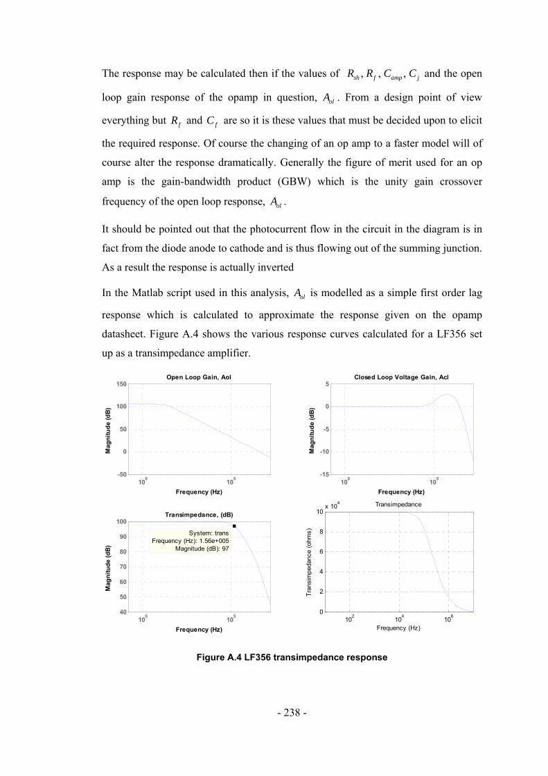
- 238 -
The response may be calculated then if the values of , , , sh f amp jR R C C and the open
loop gain response of the opamp in question, olA . From a design point of view
everything but fR and fC are so it is these values that must be decided upon to elicit
the required response. Of course the changing of an op amp to a faster model will of
course alter the response dramatically. Generally the figure of merit used for an op
amp is the gain-bandwidth product (GBW) which is the unity gain crossover
frequency of the open loop response, olA .
It should be pointed out that the photocurrent flow in the circuit in the diagram is in
fact from the diode anode to cathode and is thus flowing out of the summing junction.
As a result the response is actually inverted
In the Matlab script used in this analysis, olA is modelled as a simple first order lag
response which is calculated to approximate the response given on the opamp
datasheet. Figure A.4 shows the various response curves calculated for a LF356 set
up as a transimpedance amplifier.
102 104 1060
2
4
6
8
10x 104 Transimpedance
Frequency (Hz)
Tran
sim
peda
nce
(ohm
s)
Open Loop Gain, Aol
Frequency (Hz)
Mag
nitu
de (d
B)
100 105-50
0
50
100
150Closed Loop Voltage Gain, Acl
Frequency (Hz)
Mag
nitu
de (d
B)
100 105-15
-10
-5
0
5
Transimpedance, (dB)
Frequency (Hz)
Mag
nitu
de (d
B)
100 10540
50
60
70
80
90
100
System: trans Frequency (Hz): 1.56e+005
Magnitude (dB): 97
Figure A.4 LF356 transimpedance response

- 239 -
The 3 dB point is seen to be placed at 1.56 kHz when the value of fC was adjusted
for the maximum frequency response without gain peaking. The values of the various
parameters are given in Table A.1.
Parameter Value
shR 5 GΩ
fR 100 k
ampC 3 pF
jC 1 pF
Table A.1 Parameter values for non-peaking response
A.2 Noise Analysis of a Transimpedance Amplifier
The noise contribution of the detection circuitry is of great importance in any electro-
optical instrumentation. The aim in the design is that the performance here should be
shot noise limited so that the detection circuitry has do deleterious effect on the
measurement, that is it should provide a clear ‘window’ for viewing the
interferometer output. This section will consider first the LF356 based
transimpedance amplifier used in the instrument in chapter 5 and then compare its
performance with a circuit using a THS4062 based amplifier used in chapter 7.
First it useful to consider a general noise model for a transimpedance amplifier as
shown in Figure A.5.
Figure A.5 Transimpedance amplifier noise model

- 240 -
The majority of the noise sources are modelled as equivalent current sources (referred
to input) and as such are amplified by the closed loop transimpedance just as the
photocurrent is. , , , sig fl amp shI I I I and thI are the signal photocurrent, flicker noise
contribution, amplifier current noise, shot noise and thermal noise. In addition there
is an amplifier voltage noise whose amplification is governed by the closed loop
voltage gain. All the noise sources have a Gaussian pdf and as such there statistics are
relatively easy to determine.
The procedure for analysis is to derive the power spectral density (PSD) for each
noise contribution. The current noise contributions then modified by the
transimpedance response of the amplifier circuit attain the output PSD due to current
noise. This operation may be conveniently carried out in the s domain as a
multiplication the transimpedance response derived in appendix A.1,
( ) ( ) ( )I sig amp shot thS s G s G s I I I I′ ⎡ ⎤= + + +⎣ ⎦ (A2.0)
Conversion from the s domain (complex frequency) to the frequency domain is then
necessary. This is done easily by considering that s jω= so that an alternative
phasor representation may be written,
( ) ( ) ( ) ( ) ( ) ( )j jI I I IS s S j S j e Sφ ωω ω ω φ ω= = = ∠ (A2.1)
As we are only interested gain information it is possible to simply discard the phase
information.
The mean square noise voltage measured at the output due to current noise is then,
( )2
1
22
2
f
i Ife S d
π
πω ω= ∫ (A2.2)
where 1f and 2f form the measurement bandwidth limits in hertz, which are taken in
this analysis to be 90.1 1 10f≤ ≤ × since the measurement cycle lasts less than ten
seconds and 1 GHz is far above the low pass filtering of later circuit stages. In this
sense it represents a worse case range.
The approach for voltage noise sources is similar except it is amplified by closed loop
voltage gain of the transimpedance amplifier circuit used. Since there is only one

- 241 -
voltage noise source present, ampV the mean squared voltage noise at the output is
simply,
( )2
1
2v Ie S d
ω
ωω ω= ∫ (A2.3)
Flicker noise must also be considered but by its nature it is only relevant in the first 4
decades of operation after which it becomes much less than other noise sources such
as thermal or amplifier noise. The mean square flicker noise may be approximated by
( )22 1ln /fl fe K f f= (A2.4)
where fK is the PSD at 1 Hz. For 4 decades of operation, that is between 0.1 Hz and
1 kHz the mean square voltage noise is
2 9.210fl fe K= (A2.5)
The flicker noise associated with the op amp is a voltage and is thus amplified by the
closed loop voltage gain. However at the low frequencies considered that gain is
simply one. Hence the flicker noise contribution is generally negligible.
The total rms noise voltage as seen at the output due to all noise sources within a
transimpedance amplifier is from (6.15) written as,
2 2 2tot v i fle e e e= + + (A2.6)
A worked analysis of the LF356 based circuit used in chapter 5 is now presented.
This is then followed by simulation results for both a LF356 and THS4062 (as used
in chapter 7) based circuit.
Shot Noise
There shot noise contributions associated with both the dark current, dki flowing
through the photodiode and the photocurrent, phi . The total shot noise spectral
density is
( ) ( )2sh ph dkS f e i i= + (A2.7)
- 242 -
where /dk bias shi V R= and is set by the amount of reverse bias applied to the
photodiode. 191.602 10e −= × and is the charge on an electron in coulombs. It can be
seen that there is a trade off between increasing speed by increasing the reverse bias
voltage and the addition of dark current shot noise to the output. There is no
frequency dependence since shot noise is white noise and is thus constant across the
bandwidth.
Evaluating A2.7 for 5 VbiasV = − and 5 GshR = Ω taken from the circuit design and
assuming 40 Aphi μ= , as taken from experimental observation of the instrument in
practice,
( ) ( )6 9 24 22 40 10 1 10 12.82 10 A / HzshS f e − − −= × + × = ×
Thermal Noise
Each resistance in the transimpedance circuit produces a thermal noise current
contribution. The thermal noise associated with the feedback resistor, fR may be
placed equivalently in the same orientation as that associated with the photodiode
shunt resistance shR . The combined thermal current noise spectral density of the two
resistors is then
( ) 1 14th Bf sh
S f k TR R
⎛ ⎞= +⎜ ⎟⎜ ⎟
⎝ ⎠ (A2.8)
where Bk is Boltzmann’s constant ( 23 11.38 10 JK− −× ) and 300 KT = is the operating
temperature in Kelvin. For 5 GshR = Ω and a typical value of 50 kfR = Ω the
spectral density is then
( ) 25 23 9
1 14 1.656 10 A / Hz50 10 5 10th BS f k T −⎛ ⎞= + = ×⎜ ⎟× ×⎝ ⎠
(A2.9)
These first set of noise sources are all constant for a given input light intensity while
the following are dependent upon the specific opamp IC used. The LF356 (or dual
version, LF355) is considered in this next section, while later results will also show
the analysis for a circuit based upon the THS4062 used in chapter 7.

- 243 -
Amplifier Current Noise
This information may be gleaned from the opamp datasheet and is considered to be
constant across all frequencies. For the LF356 it is found that
( ) 28 21 10 A / HziampS f −= × . (A2.10)
Amplifier Voltage Noise
This is given in the datasheet as
( ) 16 22.25 10 V / HziampS f −= × (A2.11)
Flicker Noise
This can be approximately modelled as a set noise contribution and added on at the
end of the analysis. The mean squared voltage noise contribution over 4 decades
using a datasheet value 1512.1 10pK −= × is,
2 13 21.114 10 Vfle −= × (A2.12)
This is seen to be insignificant compared to the other noise source contributions from
the simulation and as such is conveniently ignored.
Figure A.6 shows the results of the noise simulation for both a LF356 based op amp
as well as a THS4062 op amp. Figure A.7 also show the bandwidths of these circuits
in order make a performance comparison. In each simulation the value of the
feedback capacitor was adjusted for a minimal amount of gain peaking and thus
maximum frequency response. This will yield worst case values for noise as it is
always possible to damp the response further.
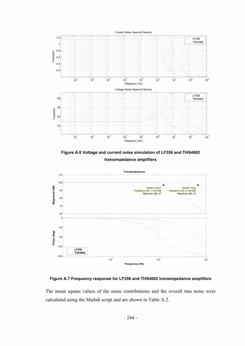
- 244 -
101
102
103
104
105
106
107
108
109
0.2
0.4
0.6
0.8
1
1.2
Current Noise Spectral Density
V/s
qrt(H
z)
Frequency (Hz)
101
102
103
104
105
106
107
108
109
10
20
30
40
Voltage Noise Spectral Density
Frequency (Hz)
V/s
qrt(H
z)
LF356THS4062
LF356THS4062
Figure A.6 Voltage and current noise simulation of LF356 and THS4062 transimpedance amplifiers
Transimpedance
Frequency (Hz)
Phas
e (d
eg)
Mag
nitu
de (d
B)
105 106 107-180
-135
-90
-45
0
LF356THS4062
LF356THS4062
60
70
80
90
100
110
System: trans1 Frequency (Hz): 1.27e+006
Magnitude (dB): 97
System: trans Frequency (Hz): 6.74e+006
Magnitude (dB): 97
Figure A.7 Frequency response for LF356 and THS4062 transimpedance amplifiers
The mean square values of the noise contributions and the overall rms noise were
calculated using the Matlab script and are shown in Table A.2.
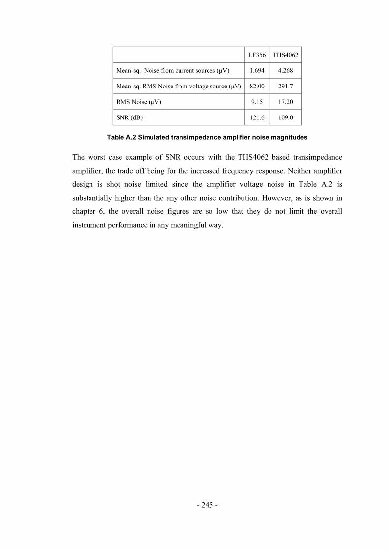
- 245 -
LF356 THS4062
Mean-sq. Noise from current sources (μV) 1.694 4.268
Mean-sq. RMS Noise from voltage source (μV) 82.00 291.7
RMS Noise (μV) 9.15 17.20
SNR (dB) 121.6 109.0
Table A.2 Simulated transimpedance amplifier noise magnitudes
The worst case example of SNR occurs with the THS4062 based transimpedance
amplifier, the trade off being for the increased frequency response. Neither amplifier
design is shot noise limited since the amplifier voltage noise in Table A.2 is
substantially higher than the any other noise contribution. However, as is shown in
chapter 6, the overall noise figures are so low that they do not limit the overall
instrument performance in any meaningful way.

- 246 -
A.3 Discretisation of an Analogue PI Controller
The discrete model is formed by taking the s-domain format and converting it using
z-transforms to produce a discrete time version.
For the plant, ( )pG s in series with a zero-order-hold, ( )pG s to model the effect of
sampling:
(1 ) 1( ) ( )(1 )
sT
o p pp
eG s G s Ks sτ
− ⎛ ⎞−= ⋅ ⋅⎜ ⎟⎜ ⎟+⎝ ⎠ (A3.0)
Where T is the sampling interval, pτ the process time constant and pK , the process
gain. After simplification, and using standard transform tables, the overall discrete
time z-domain function is;
1( )T
p
Tp
peG z K
z e
τ
τ
−
−
⎛ ⎞−⎜ ⎟=⎜ ⎟−⎝ ⎠
(A3.1)
A series PI controller takes the form:
( )1c c
z AG z Kz+=−
(A3.2)
Where 1i
TAτ⎛ ⎞= −⎜ ⎟⎝ ⎠
and iτ is the integrator time constant. cK is the controller gain.
It can be shown that such a controller may be implemented by the following recursive
formula;
[ ]1 0 1n n c n ny y K k e e+ += + − (A3.3)
Where ny is the controller output and ne is the error value.
0 1i
Tkτ
⎛ ⎞= +⎜ ⎟⎝ ⎠
(A3.4)

- 247 -
The formula above was coded for the DSP hardware and was shown to execute in
approximately 500ns. While this is very good (yielding a sample rate of 2 Mhz), the
actual sample rate is limited by the digital to analogue converter (DAC).

- 248 -
B Electronic Hardware
B.1 Introduction
This section outlines the design of the various electronic hardware used throughout
this work.
B.2 Proportional-Integral Control Circuit
Description of Operation
National Semiconductor LF356 and LF355 (dual version) op amps are used to
provide most functions in the circuit. In addition a circuit switching interface is
provided using the MAX313CPE analogue switch IC which allows elements of the
circuit to be switched in and out from a remote PC hosting a DAQ card with digital
outputs.
A summary of circuit subsections follows and is given logically by individual IC
function. All analysis is considered for ideal op amp behaviour to simplify the
description.
IC1
Input unity gain buffer with adjustable attenuation using VR4. The input signal is
obtained from a transimpedance amplifier connected to the reference interferometer
output.
IC2B
Unity gain subtractor which subtracts the input voltage from the setpoint input to
generate the error signal.
error set pdV V V= − (B.0)
IC5A
This is a simple unity gain inverter which inverts the error signal. In this manner it
can be seen that non-inverted and inverted error signals are available at ports A2 and
A1 respectively. This is used to provide the setpoint switching required as either
signal may be directed to port B by a suitable selection logic at DAQ1(TOGGLE)

- 249 -
and DAQ2(TOGGLE). It should be noted that the logic must always take opposing
values at those inputs.
IC3A
Integration stage which integrates the error signal thus getting rid of steady state
error.
1 2 10I errorV VR C V dt= − ⋅ ∫ (B.1)
The values given provide a range of integration gain, 10 iK< < ∞ (Hz).
IC3B
Proportional part of the PI controller it is a simple inverting amplification stage.
312P error
VRV VR
= − (B.2)
This supplies a range of proportional gain, 0 4.8pK< <
IC5B
Provides an inverting unity gain summation stage to add the P and I components
together.
( )2PI I PV V V= − + (B.3)
Output from the stage is directed to port C which may be switched on and off by the
appropriate logic voltage applied to port DAQ4(S/P ENA). This allow the control
loop to be effectively switched off which is necessary when modulating the PZT in
order to determine fringe visibility.
IC4A
This stage provides a secondary input for applying a signal directly to the PZT. This
provides simple method of modulating the PZT for the purposes of determining
fringe visibility. A triangular wave signal is applied to the offset input when the
control loop is disabled in order to perform this function. VR6 provides gain
adjustment.
IC4B

- 250 -
This stage simply sums the outputs from the PI controller stages and the offset input
stage. In normal operation only one input is actually present at any one time.
IC6
This is a unity voltage gain stage which has a BUF634T current amplifier inside its
feedback loop. This effectively provides a current boosting which raises the 40 mA
compliance of the LF356 op amps to 250 mA to ensure the PZT is not slew rate
limited because of the driving electronics.
MAX313CPE
This IC provides analogue switching for the various reasons outlined in the preceding
sections. It takes inputs from the DAQ in the form of TTL compatible voltage levels.

- 251 -
PI Controller Circuit Diagram
Figure B.1 PI Controller Circuit Diagram
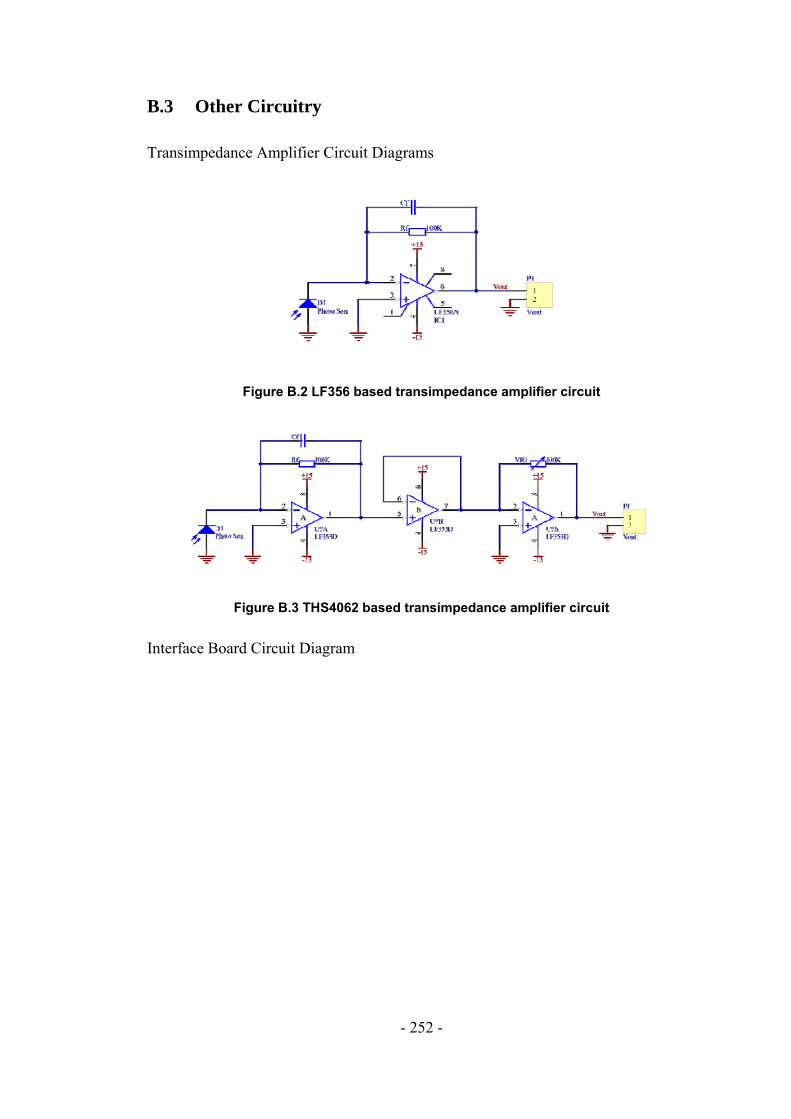
- 252 -
B.3 Other Circuitry
Transimpedance Amplifier Circuit Diagrams
Figure B.2 LF356 based transimpedance amplifier circuit
Figure B.3 THS4062 based transimpedance amplifier circuit
Interface Board Circuit Diagram

- 253 -
Figure B.4 Interface Board Circuit Diagram
Laser Diode Driver
Figure B.5 Laser Diode Driver
EOPM Driver and Logic Level Translator Diagram

- 254 -
Figure B.6 Driver and Logic Level Translator Circuit Diagrams
B.4 Rapid Phase Shifting Functional Overview
Input and output for the circuits are shown as pin numbers (or names where
applicable) at the perimeters of the main boxes. The italicised names correlate to the
header designations on the circuit diagrams in appendix B1-3. The arrows on the

- 255 -
diagram indicate the direction of dataflow. Software is represented by the dashed
boxes.

- 256 -
C Noise Theory
C.1 Definition of Noise
Noise may be defined simply as any unwanted signal in a system. This definition is
where the simplicity ends unfortunately since the sources of noise affecting an
electro-optic instrument are wide ranging in there type and severity. Noise may be
characterised as a random signal and produced from a stochastic process.
Defining noise mathematically relies upon the use of probability theory and random
variables and it is useful to consider some of the basic terminology. The probability
of some random variable X assuming some discrete value ( )1, 2,3...iX i = occurs in
times in a total number of N results,
( ) lim ii N
nP XN→∞
= (C.1)
For the case of a continuous random variable, the probability that X is in some
range, XΔ centred about iX is then,
( ) ( )2 2 lim iX Xi i i N
nP X P X X XN
Δ ΔΔ →∞
= − < ≤ + = (C.2)
where in is now the total number of outcomes in the range 2X
iX Δ− to 2X
iX Δ+ for a
total number of N results. It is more useful however to consider the limit 0XΔ → by
which one derives the continuous probability density function (PDF),
( )0
( ) lim i
X
P Xp X
XΔ
Δ →=
Δ (C.3)
It is now possible to say that the probability of X falling in the range 1 2X X→ is
( ) ( )2
1
1 2
X
X
P X X X p X dX< ≤ = ∫ (C.4)
where by definition
( ) 1p X dX∞
−∞
=∫ (C.5)
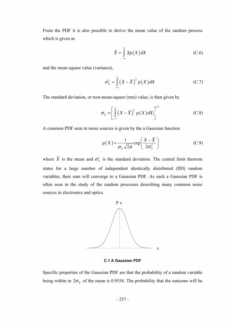
- 257 -
From the PDF it is also possible to derive the mean value of the random process
which is given as
( )X Xp X dX∞
−∞
= ∫ (C.6)
and the mean square value (variance),
( ) ( )22X X X p X dXσ
∞
−∞
= −∫ (C.7)
The standard deviation, or root-mean-square (rms) value, is then given by
( ) ( )1/2
2X X X p X dXσ
∞
−∞
⎡ ⎤= −⎢ ⎥⎣ ⎦∫ (C.8)
A common PDF seen in noise sources is given by the a Gaussian function
( ) 2
1 exp22 XX
X Xp Xσσ π
⎛ ⎞−= ⎜ ⎟⎝ ⎠
(C.9)
where X is the mean and 2Xσ is the standard deviation. The central limit theorem
states for a large number of independent identically distributed (IID) random
variables, their sum will converge to a Gaussian PDF. As such a Gaussian PDF is
often seen in the study of the random processes describing many common noise
sources in electronics and optics.
x
Px
C.1 A Gaussian PDF
Specific properties of the Gaussian PDF are that the probability of a random variable
being within in 2 Xσ of the mean is 0.9554. The probability that the outcome will be

- 258 -
within 3 Xσ either side of the mean is 0.9973. This leads directly to the useful rule of
thumb derived for noise exhibiting a Gaussian PDF; the peak to peak noise value will
be 6 times the rms noise value.
For the study of noise one is generally concerned with not just a single number but
with a random function in time. The production of a random function in time is
termed a stochastic process. A wide sense stationary random process is one in which
the mean and autocorrelation function are independent of time. It is then possible to
say that the mean or expected value of X at a time t for a random process normally
given by
( ) ( ) ( );X t X t Xp X t dXε∞
−∞= =⎡ ⎤⎣ ⎦ ∫ (C.10)
may be simplified to
[ ] ( )X X Xp X dXε∞
−∞= = ∫ (C.11)
while the expected value of the mean square of x is
( )2 2 2X X X p X dXε∞
−∞⎡ ⎤= =⎣ ⎦ ∫ (C.12)
If the process is also ergodic then the complete statistics for that random process may
be derived by time averaging. All the noise signals to be considered in this chapter
are wide sense stationary and ergodic and as such the time dependence of all
statistical properties is removed.
The autocorrelation for an ergodic stationary random process is given by
( ) ( )( ) ( )( )[ ] ( )( ) ( )( )XXR X t X X t X X t X X t Xτ ε τ τ= − + − = − + − (C.13)
where the expected value is derived from time averaging over a long period. When
the time shift 0τ = the peak of the autocorrelation is found.
( ) ( ) 20XXR X t X⎡ ⎤= −⎣ ⎦ (C.14)
For zero mean processes it is clear from Error! Reference source not found. that
the peak of the autocorrelation is equal to the variance. In general it is possible to

- 259 -
deduce any Gaussian PDF as long as you know the mean and the autocorrelation of
the random process.
The auto-correlation of a signal is seen to be related to its power-spectral density
(PSD) by the Wiener-Khinchin theorem. This is an analogous relationship to that of
linewidth and coherence time for an optical wave as discussed in section 3.4.6.
( ) ( ) ( ) 12
S S Rω ω τ′= = ℑ (C.15)
where ( )S ω and ( )S ω′ are the bilateral and unilateral PSDs respectively.
Because a linear system driven by a signal with a Gaussian PDF will have an output
signal with a Gaussian PDF it is possible to determine the nature of the output if the
frequency response of the system in known. In fact all statistical properties of interest
e.g. mean, rms may all be derived.
The general practice when dealing with noise sources having a Gaussian PDF is to
use the rms values. This is due to the fact that uncorrelated noise sources are added
using root-sum-square addition such that,
2total
1
k
ke e= ∑ (C.16)
where ke is the rms value of the thk uncorrelated noise source.
Because of this the summation it is this found that in any system there are generally a
reduced set of noise sources whose rms values contribute to a much larger portion of
the overall rms noise value. Hence any noise reduction strategy will tend to pinpoint
these first and attempt to reduce or eliminate them. After this process the effect of
more minor sources then starts to become significant. In general, the contribution of a
noise source whose rms is less than a third of the highest rms value in a set of
uncorrelated noise sources is negligible.
Signal to noise ratio is often an important quantity for the analysis of noise as it
yields a generalised parameter for comparison. It is defined as
2
sigPSNR
Xε=
⎡ ⎤⎣ ⎦ (C.17)

- 260 -
where sigP is the signal power and 2Xε ⎡ ⎤⎣ ⎦ is the expected value of the variance of
the noise signal. Generally SNR is written as a decibel value and in terms voltages for
electrical usage,
( ) 20log sig
n
VSNR dB
e⎛ ⎞
= ⎜ ⎟⎝ ⎠
(C.18)
where sigV is the signal voltage and ne is the rms noise voltage.
Noise sources magnitudes often also have a frequency dependence, either inherent in
the process or due to filtering at detection. Even though white noise sources
theoretically have a flat band noise power spectral density (PSD) that extends to an
infinite frequency, the reality is that it will be filtered by the various components of
the instrument. An example of this is the flat band thermal noise of a resistor in an
electronic op amp circuit. Such a noise source is often modelled as a voltage source
for analysis purposes and in order to derive the correct rms values for the total noise
at the circuits output we must integrate under the power spectral density. In theory
the PSD extends to infinity, thus so must the rms noise power. To calculate realistic
noise values one must consider the bandwidth in which the op amp circuit operates
and truncate the PSD accordingly. Well thought out filtering strategies are vital
throughout an instrument, regardless of the domain under consideration be that
optical, electrical or mechanical.
C.2 Electronic Noise Types
This section outlines relevant electronic noise sources and quantifies there likely
magnitudes where possible.
Shot Noise
Shot noise is a fundamental noise source that is related to the fact that an electric
current is made up of discrete charge carriers. Shot noise is the statistically
uncertainty surrounding the measurement of any electric current. ‘Full’ shot noise
occurs only in certain situations, where the charge carriers act independently of each
other. One relevant case is in the flow of charge carriers across a junction where the
movement occurs through the process of diffusion. This is significant in the
- 261 -
photocurrents produced by photodiodes, especially when coupled with the fact that
the generated currents are often very small.
The full shot noise exhibited by a photocurrent generated by a photodiode may be
shown to have a root normalised power spectral density of;
2n pi qI= (C.19)
where q is the charge on the charge carrier (in this case an electron), pI the mean
photocurrent generated. The noise forms a Gaussian distribution for any appreciable
quantity of photoelectron creating events and as can seen from
Error! Reference source not found. it is constant for all frequencies; as such it is
white noise.
Charge carriers flowing through metallic conductors do not exhibit independent
behaviour, the result of which is that they show much less than full shot noise.
The term ‘shot noise limited’ is often used to describe an instrument were all other
noise sources have been reduced to below this fundamental level; in this sense the
instrument is performing optimally.
Thermal (Johnson) Noise
Johnson noise results from the random agitation of electrons in a conductor and is
always present, depending only on the temperature and resistance of the conductor.
This noise is white noise for all practical frequencies of operation and Gaussian in
distribution. In circuit theory, the noise may be modelled by a noise source in series
with a perfect, noiseless resistor. The spectral density is a useful interpretation for the
purposes of analysing transimpedance amplifiers;
( ) 4 bth
k TS fR
= (C.20)
where T is the temperature, R the resistance and bk Boltzmann’s constant. Good
circuit design can generally ensure that the Johnson noise contribution to the output
of a detection circuit remains below that of shot noise in applications where
bandwidth and amplification requirements not overly challenging.

- 262 -
1/f, Flicker or Excess Noise
1/f noise is any noise type that has equal power per frequency decade, it may also be
called pink noise, flicker noise or excess noise. 1/f noise occurs in many situations
such as the base current of transistors and in the resistance of a resistor. It also occurs
in a wide ranging array of other situations completely unconnected with electronics.
The sources of 1/f noise are as varied as the situations in which it is found, sometimes
a specific mechanism may be determined for a given case. From the point of view of
building optical instrumentation one is concerned with its contribution in long term
and baseband type measurements. Excess noise is of importance only over the
frequency range where it is higher than the thermal or shot noise contributions. Any
circuit will lowpass filter flicker noise by virtue of the fact it will be turned off at
some interval. Excess noise has a Gaussian pdf and a normalised spectral density of
( ) ffl
KS f
f α= (C.21)
where fK is value of the spectral density at 1 Hz and α depends on the application
and can vary in value between 0.8-1.4, but is generally approximated to unity for
practical purposes. The mean square noise voltage over a frequency range
1 2f f f≤ ≤ is then
( ) ( )2
12 1/ ln /
f
fl f ffe K f df K f f= =∫ (C.22)
Burst (Popcorn) Noise
Occurring in semiconductors, its origins are not completely understood. It appears to
be linked to impurities in the semiconductor material and causes random step changes
in voltage or current levels. It is random and unpredictable making it very difficult to
design contingencies for its occurrence. The reduction of popcorn noise in
semiconductor devices is done by screening the finished products; thus the purchase
of quality screened semiconductor devices is the best way of mitigating the effects of
popcorn noise.
Amplifier Noise

- 263 -
Amplifier noise lumps voltage and current noise and is a catch all term used to
provide a general idea of the noise to be expected when using commercial electronic
ICs. Information is generally to be found on the datasheet, and is often given in the
graphical form of a power spectral density plot. Such noise sources are generally
referred to input, that is the data given is for a current/voltage noise source applied to
the input terminals of an amplifier. The circuit design which determines the
frequency response of the amplifier will affect how this noise is amplified at the
output.
Quantisation Noise
The reality of most optical instrumentation is that the analogue signals obtained will
at some point be sampled and digitised in order that they may be processed, stored
and displayed by computer. The act of digitising signals adds results in the addition
of quantisation noise to a signal. There are two essential types of quantisation,
rounding and truncation.
Rounding generally occurs in the analogue to digital conversion, the analogue signal
being rounded to the nearest discrete level on conversion. This leads to a maximum
possible error of 12 LSB± (least significant bit).
Truncation can occur during floating point computation, especially when a
multiplication takes place and the LSBs of the result must be truncated in order to be
stored in a register. The maximum possible error through truncation is 1 LSB.
The range of analogue voltages present between the LSB of the analogue-to-digital
converter (ADC) is critical in determining the scale of quantisation noise present. The
quantisation band q represents the range covered by 1 LSB and is given by
2N
Vq Δ= (C.23)
where VΔ is the voltage range covered by the ADC and N is the number of bits
used in the digitisation process. Clearly the input signal must be conditioned so that
its peak to peak range equal to the full scale voltage range of the ADC or the
effective value of q will be smaller.

- 264 -
The two areas of optical instrumentation where the injection of quantisation noise
will affect operation are in the final accuracy of data captured, and in the action of
any discrete time control loops that may be implemented.
Due to the quantisation process and in the absence of the other noise sources, the
maximum resolution of the instrument is given by the measurand change that will
instil a variation of 2q in the analogue signal.
In a control loop it is possible that quantisation noise could produce non-optimal
performance and even lead to instability. However in well designed robust control
systems the noise will be well within the maximum parameter variation boundaries.
The use of a digital-to-analogue converter (DAC) in control loops to produce the
actuating signal also creates additional quantisation noise if the resolution of that
DAC is less than the numerical resolution used for the preceding computation. This
will result in a maximum resolution for servo control which if too large may cause
settling problems and unstable operation.
The effects of quantisation are much more complicated than the relatively simple
process itself might suggest. It is unusual to fully analyse all the effects throughout a
control system as often the effects are negligible. There are danger areas where
quantisation noise can be serious such as when it precedes a large gain.
Consider an analogue signal that is to be digitised, its value can be anywhere between
2q± once digitised will be and the error between the continuous and digitised signal
can be considered as a noise source. The error probability distribution can be
considered to be constant within the band formed by q which is practically
justifiable, although only strictly correct for non-deterministic signals. The expected
value of the error, ( )E e is seen to be zero in the case of rounded digitising processes
(such as those in an ADC). The variance is then,
( ) ( )/23 2
22 2
/2
1 1var( )3 12
q
q
e qe E e E e e deq q
+
−
= − = = =⎡ ⎤⎣ ⎦ ∫ (C.24)
Generally other distortions and noise processes will conspire to reduce the SNR of an
ADC below the ideal level.

- 265 -
The DAQ card using the instrument in chapter 5 has an ADC resolution of 16 bits.
However the onboard ADC on the DSP card used in the instrument in chapter 7 has
only 12 bit resolution hence this value will be used for worst case analysis. The
datasheet SNR for the onboard ADC is 62 dB for full scale operation.
The obvious way of reducing these effects is to increase the resolution of the ADCs
and DACs used in the system, possibly at the expense of sampling rate and added
complexity. Within the bounds of a given resolution it is essential to use appropriate
signal conditioning prior to the digitisation to ensure the full range of an ADC
utilised. Good coding of algorithms will ensure that finite word length errors will be
of little consequence to the overall operation.
C.3 Optical Noise Types
This section outlines relevant electronic noise sources and attempts to quantify their
likely magnitudes where possible.
Relative Intensity Noise (RIN)
RIN is the fluctuation in laser output relative to its mean output and is a catch all term
for the contributions of various processes. RIN is generally defined as the noise over
and above the shot noise level that forms the ultimate noise floor. As suggested by its
name, RIN is measured relative to the actual output power from the source. Some
early experimental measurements of RIN occurring in semiconductor lasers, with
application to interferometry, were made by Dandridge at al. (1980).
The power spectral density (PSD) for semiconductor lasers is generally found to be at
its highest up to several tens of megahertz and the falls toward the shot noise level at
higher frequencies. A resonant peak in the RIN PSD may well be observed due to
relaxation oscillations in the laser cavity. RIN specifications are usually given in dBc
which is the power fluctuation, PΔ relative to the carrier power cP .
( ) 10 logc
PRIN dBP
⎛ ⎞Δ= ⎜ ⎟⎝ ⎠
(C.25)

- 266 -
The RIN specification for the Ando AQ4320 is given as -145 dBc/Hz which as no
information is given on the PSD shape is assumed to be flatband. The rms RIN over a
7.85 MHz bandwidth is then,
145/10 6 410 7.85 10 1.575 10rms cP P− −= × × = × ⋅ (C.26)
The 7.85 MHz bandwidth value is chosen as it is the brick-wall equivalent
bandwidth for a single pole filter response for a 5 MHz cut frequency, as exhibited by
the fastest transimpedance amplifier used in this thesis. As such this provides a worst
case figure and equates to an optical SNR of
0 4
1( ) 10log 38.03 dB1.575 10
SNR dB −⎛ ⎞= =⎜ ⎟×⎝ ⎠
(C.27)
It should be noted that SNR is a power ratio but the square law nature of the PIN
detector converts optical power into amplitude (voltage). As such, the equivalent
electrical SNR value is,
( )20eSNR SNR= (C.28)
which means one simply doubles the optical SNR quantity in decibels to arrive at an
electrical SNR of 76.1 dB for the RIN noise contribution.
The distributed Bragg reflector laser diode (see section 4.6.6) used as the reference
source can be expected to perform as well as the external cavity based Ando AQ4320
tuneable laser in terms of RIN assuming it is driven by a stable low noise current
source.
Source Phase Noise
Phase noise is the random variation of phase in the output of laser source. One effect
is to cause a broadening of the linewidth of a laser source and thus a corresponding
reduction in the coherence length of the source. In interferometric applications, phase
noise is converted directly into fringe intensity variation over time, reducing its
definition and thus the resolution of the instrument. This is usually modelled as the
reduction of the SNR, the effect of which is added to the RIN derived in section
Error! Reference source not found..
- 267 -
Petermann and Weidel (1981) derived the spectral density functions for intensity
noise at the output of an interferometer due to phase noise for the specific case of in-
quadrature operation. Early experimental measurements on a range of laser diode
were made by Dandridge and Tveten (1981). Moslehi (1986) extended the theoretical
analysis of the phase noise of a single mode laser diode operating at any bias point.
Salehi and Cabon (2004) then further considered the effects of dispersion on the
results for long fibre lengths (tens of kilometres). Cliche and Têtu (2005) considered
the effects of linewidth reduction systems on the phase noise.
Since the length of fibre being considered in the instruments in this thesis is relatively
short, the effects of dispersion may be neglected. Also as the maximum sensitivity to
phase noise occurs at the quadrature operating point, it is reasonable to use definition
for the PSD of intensity noise occurring due to phase noise. An approximation, given
by Moslehi (1986), for the bilateral spectral density is valid in the coherent regime in
which the instruments operate,
( ) ( )22
20 sinc2ph
c
TIS f fTτ
≈ (C.29)
where T is the differential time delay between the interferometer arms, cτ is the
coherence time and 0I is the input power.
Taking the PSD profile of the laser output to be Lorentzian, and knowing the FWHM
to be 1 MHz (Ando AQ430D), it is possible to determine the coherence time using
the definition given in section 3.4.6 as
6
1 318.3 ns1 10cτ π= =×
(C.30)
Given that the interferometers are only being considered over one full fringe we can
consider the largest differential time delay as being at the full extent of the range,
which in the case of 1550 nm operating wavelength is 775 nm. The equivalent time
delay is,
2.583 fsnlTc
= = (C.31)

- 268 -
bearing in mind that the added imbalance takes place in free space. Over the
frequency range at which either instrument operates the maximum frequency
is 7.85 MHzf = . Over this range it is found that ( )2sinc 1fT ≈ and
Error! Reference source not found. becomes,
( )22
0
2Ic
TIS fτ
≈ (C.32)
Since the power spectral density is approximately constant over the bandwidth, the
normalised rms value of the amplitude noise is then simply given by,
( )2
82.566 10phc
T fS f
τ−Δ
≈ = × (C.33)
where 7.85 MHzfΔ = is the full bandwidth of operation. This gives an electrical
SNR of 168.1 dB at the detector.
Although the effect of linewidth broadening may result in fringe definition being
reduced, the associated reduction in coherence length can actually be beneficial from
the point of view of fibre interferometers resulting as it does in reduced etalon fringes
by eliminating some of the coherent mixing.
Etalon Fringes
An etalon is an optical resonator (or cavity) formed from planar reflectors. Etalons
see wide use as high finesse filters (such as the Fabry-Pérot interferometer) where the
reflectors are partially silvered mirrors separated in air. However an etalon may just
as well be formed from a solid piece of transparent material; the Fresnel reflection
caused by the discontinuity of the refractive index at the material – air boundary of
the facets results in the formation of an etalon.
Etalons formed between any two surfaces in an optical system can cause major
headaches in instrument utilising coherent light, especially when dealing with fibre
optics. In general, the reduction of etalons is done by using suitable coatings on
surfaces to reduce reflections and the deliberate misalignment of surfaces (canting) to
ensure the reflections end up somewhere harmless.

- 269 -
Each etalon acts as an interferometer and has the effect of causing FM-AM
conversion of the light due to the interference of light with delayed copies of itself. In
the case of fibre optics, each connection between fibres/integrated optic components
results in the creation of multiple etalons. Furthermore, the spatial coherence is
extremely high in single mode fibres due to the exact alignment and the Gaussian
wavefront of the single guided mode. There is no ‘washing out’ (averaging) of the
fringes over the wavefront; thus the interference produces a fringe with almost full
contrast. This means that even relatively low levels of back reflected light from
etalons can cause severe problems with generated intensity noise (Hobbs p243).
Any source phase noise is converted to amplitude noise by each etalon in the system,
the magnitude of the noise being dependent upon the etalon length and the strength of
the reflections. Reducing the linewidth of the source does not necessary help matters
because the associated increase in coherence length can result in more etalons being
setup.
The longer the coherence length of the light source, the more etalons that can mix
coherently, further compounding the problem. In this case, a broader linewidth source
may be beneficial for reducing this effect, at the expense of added phase noise.
Reducing etalon fringes in fibre requires the reducing the back reflection occurring at
any interfaces within the optical circuit. Any point in the circuit has a refractive index
differential can form an etalon. Fibre connectors, used to facilitate the coupling of
lengths of fibre together are often the worse candidates. In addition, any fibre linked
integrated-optic device will suffer from back reflection at the fibre-waveguide
interface.
Return loss (or reflection loss) is that loss in power of a transmitted signal due to
reflection at an interface. In optical terms return loss describes the amount of power
reflected back from a refractive index discontinuity. The return loss, RL in decibels is
simply the ratio of the input power, iP to the reflected power, rP ;
( ) 10 log iR
r
PL dBP
⎛ ⎞= ⎜ ⎟
⎝ ⎠ (C.24)
- 270 -
One example of return loss commonly experienced in a fibre optic circuit is that
caused by the Fresnel loss between the interface of a bare fibre end, cleaved normally
to its axis, and air. The reflectivity, ℜ is the fraction of power reflected back (return
loss in this case) and is dependent on the two refractive indexes forming the interface,
0n and 1n ;
2
0 1
0 1
n nn n
⎛ ⎞−ℜ = ⎜ ⎟+⎝ ⎠ (C.25)
If Error! Reference source not found. is evaluated for a fibre to air interface where,
0 1.48n = is the index of the fibre core and 0 1n = approximates the index of air. The
reflectivity, ℜ is then seen to be 0.0375 (≈ 4%) producing a return loss of 14.3 dB,
an extremely large and problematic value.
Minimising the return loss associated with bare fibre ends is done by ensuring the end
is placed in a quantity of a suitable index matched gel. This acts as a beam dump,
ensuring the efficient coupling of the beam from the fibre and dispersing it
harmlessly. We must consider also the importance of index match between the gel
and the fibre core; a mismatch of 0.01 in their refractive indexes will result in a return
loss of 24.7 dB.
Another common place for etalon creation to occur between connectors used to
couple fibre sections together. The standard FC/PC polished connectors that are
commonly used in laboratories for the quick and easy coupling of single mode fibres
will have at best a return loss of 40 dB and this is subject to increase as the connector
wears through several mating cycles. This is decreased to 50 dB for the more highly
polished FC/UPC version and is seen to be much improved to 60 dB for the angled
FC/APC connector. The end of the FC/APC version of the connector is polished at an
angle of 8° thus ensuring that most of the Fresnel reflected light is directed back into
the fibre at above the acceptance angle and thus passes harmlessly into the cladding
rather than being guided. In addition to the use of high quality connectors, it is
possible to reduce return loss significantly, even with FC/PC connectors by applying
a suitable index matching gel to the mating faces before connecting. This is often not
suitable for field use, or where regular re-connection is anticipated; in a clean optical

- 271 -
laboratory, and with diligent cleaning between mating cycles it is an effective method
of reducing return loss.
A better way to reduce the potential for etalon creation in an optical fibre circuit is
not to use couplers at all were possible but to use a fusion splicer to join fibre lengths
wherever possible. Clearly this limits flexibility somewhat, but towards the final
stages of development of an instrument, may well prove critical.
In addition, the use of all-fibre devices should also be investigated. One example of
such a device is an all-fibre coupler. These devices are created twisting fibre together
and fusing of them. The result is to produce the same effect as an integrated optic
coupler, but because the light never leaves the fibre, return loss is generally seen to
be lower.
There are times that integrated-optic components must be used, for example an
electro-optic phase modulator (EOPM) is unavailable as an all-fibre entity. In the
case of the EOPM used in the instrument developed in this thesis (EOSpace low Vpi )
the total return loss is 50 dB. This includes the return loss from the fibre connectors
as well as the fibre-to-device interface itself.
In summary, etaloning is a serious problem in any high coherence optical instrument
but is particularly serious when dealing with optical fibres as the alignment if fixed. It
is also not feasible to give a theoretical analysis of etaloning in an instrument and in
general the solution must be reduce any back reflection at interfaces as much as
possible by paying attention to all index interfaces and coatings.
Intrinsic Fibre Phase Noise
In any optical medium the refractive index undergoes several statistical fluctuations
due to thermodynamic processes. They are more pronounced in optical systems that
have their optical paths contained in a solid material. The solid waveguide coupled
with generally long path lengths mean that fibre optic systems are particularly
susceptible to this noise type. The mechanisms involved in generating
thermodynamic phase noise are related to the larger scale difference in path length
change we see during external perturbation due to temperature drift and vibration but
generally it is treated separately due to the smaller scale mechanics involved.

- 272 -
The intrinsic fibre phase noise is results from the statistical fluctuation of density and
temperature which results in a variation of index. The two mechanisms have differing
magnitudes and frequency dependence, hence they are treated separately and then
summated to give an overall result.
The original derivation was given by Glenn (1989) for the case of a fibre with infinite
cladding. This was then considered further by Wanser (1992) who extended the
definition of the thermodynamic element to include a finite cladding diameter. This
analysis results in lower noise values at frequencies below 200 Hz. These results
were then experimentally verified by Wanser (1993). Kråkenes and Bløtekjær (1995)
considered the effects of phase noise on Mach-Zehnder and Sagnac interferometers.
Annovazzi-Lodi et al. (1996) extended the comparisons further to include the Fabry
Perot interferometer and ring resonator.
In general at low frequencies it is found that the thermodynamic fluctuation is of
much greater magnitude than the density fluctuation. It is now possible to consider
the two cases separately.
Density Fluctuation
Glenn (1989) derives spectral density of the contribution due to density fluctuation as
( )2
22 2
1 4.75 sinq
b q
V xk T q dxV T xρ ρ
φ ωυλ −
∂⎛ ⎞= − ⎜ ⎟∂⎝ ⎠ ∫ (C.26)
which is valid for the special case when 1aωυ
. bk is Boltzmann’s constant, T is
the temperature, λ the operating wavelength and 1 VV T ρ
∂⎛ ⎞⎜ ⎟∂⎝ ⎠
is the compressibility of
silica. υ is the acoustic velocity in silica and 2
lq ωυ
= where l the total length of fibre
being considered and a is the core radius.
The special case is valid when 190 MHzw and is thus valid for this analysis
considering that the highest cut frequency of the transimpedance amplifiers used is 5
Mhz.

- 273 -
The integral in Error! Reference source not found. can be approximated for all
practical purposes by qπ which leads to the simplification
( ) 2 2
1 4.752b
V lS k TV Tρ
ρ
ωωπυ λΔ
∂⎛ ⎞= − ⎜ ⎟∂⎝ ⎠ (C.27)
The mean square value of the phase noise is then simply the integral of
Error! Reference source not found. which from DC to maxf in hertz is
2 2max2 2 2
1 4.752b
V lk T fV Tρ
ρ
φπ υ λ
∂⎛ ⎞= − ⎜ ⎟∂⎝ ⎠ (C.28)
Thermal Fluctuation
Wanser (1992) gives the power spectral density of the noise due to thermal processes
in the fibre as
( ) ( ) ( )
( ) ( ) ( )
0
22 2 2222
22 2 2 22.405
S ( ) ln2
f
nw c D
bL
na c D
k T l dn ndT
ω ω
φω ω
ω ακλΔ
⎧ ⎫⎡ ⎤+ +⎪ ⎪⎪ ⎪⎛ ⎞ ⎣ ⎦= + ⎨ ⎬⎜ ⎟⎝ ⎠ ⎡ ⎤⎪ ⎪+ +⎢ ⎥⎪ ⎪⎣ ⎦⎩ ⎭
(C.29)
where κ is the thermal conductivity of the fibre, D the thermal diffusivity and α is
the linear thermal coefficient of expansion. /dn dT signifies the change in index with
temperature of the fibre while 0ω and fa are the mode field radius and outer radius
of the cladding. All other parameters are as defined for
Error! Reference source not found..
A zero frequency case is also given to correct for the effect of finite cladding
diameter for the low frequencies,
22
20
2S (0) ln
2 2.405fb
L
ak T l dn ndT wφ α
κλΔ
⎛ ⎞⎛ ⎞= + ⎜ ⎟⎜ ⎟⎝ ⎠ ⎝ ⎠
(C.30)
The result of this is a reduction in the noise magnitude for low frequencies but over
the 5 MHz bandwidth operated on by the instruments in this theory this slight
improvement below is insignificant and therefore neglected.
A typical set of values for a single mode fibre operating at room temperature and at a
wavelength of 1550 nm is shown in Table C.1Error! Reference source not found..

- 274 -
Property Notation Value
Temperature T 300 K
Temperature coefficient of
index
dndT
5 113.5 10 K− −×
Compressibility 1
T
dVV dP⎛ ⎞⎜ ⎟⎝ ⎠
10 -11/ 3.6 10 Pa− ×
Acoustic velocity υ 15962 ms−
Thermal conductivity κ ( ) 11.37 W m K −⋅
Linear expansion coefficient
Lα 6 10.41 10 K− −×
Thermal diffusivity D
6 2 -10.82 10 m s−×
Outer cladding diameter fa
125 mμ
Operating wavelength λ 1550 nm
Index n 1.468
Mode field radius 0w 10 μm
Table C.1 Parameter values for Silica
Matlab was used to plot the spectral density functions for the density and phase
contributions and the result is seen in figure C.2Error! Reference source not
found.. It is quite apparent that the temperature fluctuation contribution is much more
important at low frequencies. However there is a cross over point at around 700 kHz
after which it is seen that density fluctuation is the main contributor to the overall
noise.

- 275 -
10-1 100 101 102 103 104 105 106 107
10-25
10-20
10-15
Frequency
Mag
nitu
de ra
d2 /Hz
Spectral Densities of Instrinsic Fibre Phase Noise
ThermalDensity
C.2 Spectral Densities of intrinsic fibre phase noise contributions
Matlab was used to calculate the mean square noise values for both the density and
phase fluctuation contributions over a 5 MHz bandwidth from DC. They are
respectively,
2 15.36 μradρφ = (C.31)
2 17.76 μradρφ = (C.32)
where the fibre length is 20 m. For a Michelson interferometer this equates to a total
fibre length of 10 m since a double pass of each arm is made. The total rms
contribution is then seen to be
2 2 23.48 μradrms Tρφ φ φ= + = (C.33)
which in terms of measured height at an operating wavelength of 1550 nm is
2.896 pm4
rmsnm
λφφπ
= = (C.34)
Thermodynamic phase noise can be a serious and limiting noise source in fibre
interferometric sensors. It generally presents the noise floor for any significant
combination of fibre length and detected power. In the case of the instruments
described in this thesis it effects are not particularly debilitating because of the short
length of fibre under consideration.
C.4 Computationally Induced Noise

- 276 -
Although the various noise sources present in optical fibre interferometers have been
considered individually, it also remains to consider their effect on any signal
processing performed on the recorded intensity data. From the point of view of phase
shifting interferometry specifically, the main concern is how noise propagates
through the phase shifting algorithms that are used to derive the interferometer phase
from the raw intensity outputs.
A wide selection of phase shifting algorithms have been developed starting with the
Carré algorithm in 1966. Phase shifting algorithms all work in a similar fashion, by
solving a set of simultaneous equations provided by a multiple set of intensity
measurements taken from an interferometer at various phases (see section 4.7.8).
Their sensitivity to varying noise sources within a system is variable however and
this is one of the reasons for the multitude of different algorithms; they have different
strengths when it comes to the reduction of differing noise types (Creath 1998).
Typical variations in phase shifting algorithms are the number of shifts performed,
with the general trend being the reductions of error caused by noise in the raw data
decreasing as the shift number increases. Clearly with an increased number of phase
shifts, there is a performance hit due to increased acquisition and computation time.
In general, the lengthening of the acquisition period can result in increased
inaccuracies due to drift creeping into the measurement.
Wingerden et al. (1991) defined three noise types that can act upon a PSI algorithm
and went on to estimate their effects on numerous algorithms by using linear
approximation techniques. The three noise types defined were systematic, random
with sinusoidal dependence and random with no correlation to initial phase. They are
named as type 1, 2 and 3 noise respectively.
The noise types may be usefully represented by error terms in the interferometer
equation
( )( ) ( )( ) ( )0 1 2 31 cosI I t V t tε φ ε ε⎡ ⎤= + + +⎣ ⎦ (C.35)
where ( )N tε is a noise source of type N .
From Error! Reference source not found. it is clear where the source of each noise
type originates. Type 1 results from intensity variation (RIN) in the light source and

- 277 -
any etalon effects. Type 2 is phase noise which results from environmental
disturbance and intrinsic fibre phase noise. Type 3 is noise introduced after the
interference has taken place and is mainly the result of electronic noise introduced by
the detection front end.
A numerical simulation can provide a good indication of the behaviours of phase
shifting algorithms. Matlab simulations for each of the three noise types were carried
out and the scripts may be found in appendix C. The simulations add a random noise
having a Gaussian distribution and then monitor the resulting error induced in the
calculated output phase. The optimal Carré phase shift of 55α = ° with regard to
random noise elimination is used throughout the simulations. The simulation was
carried out with a linearly increasing phase difference between 0 and 2π to see
whether the noise output varies on the input phase. The simulation runs over 10000
samples for any given input range, thus it is possible to be confident of the results due
to the large amount of trials.
Type 1 Noise Simulation
Figure C.3Error! Reference source not found. shows the consequences of type 1
noise upon the Carré algorithm. There are several components which are clockwise
from the top left; the input phase value, the input intensities for each phase shift (after
phase noise addition), calculated phase and error in the calculated output. The input
intensities at each phase shift are represented by a seperate colour.
A relatively large amount of noise was introduced to make the effects of the noise
clear. The input noise was white noise having a Gaussian distribution, the signal to
noise ratio is 40 dB and the fringe visibility is 0.9. The issue of wraparounds is quite
evident at the extremes of the unambiguous phase range.

- 278 -
0 5000 100000
2
4
6
8Input Phase
Pha
se A
ngle
(rad
)
Sample Number0 5000 10000
0
1
2
3Fringes Intensties
Nor
mal
ised
Inte
nsity
Sample Number
0 5000 100000
2
4
6
8Calculated Phase
Sample Number
Pha
se A
ngle
(rad
)
0 5000 10000-10
-5
0
5
10Error
Sample Number
Pha
se A
ngle
(rad
)
C.3 Effect of type 1 noise showing induced wraparounds
The gross errors that occur around the 0 and 2π boundaries are due to phase wrapping
distortions. This is clearly and major issue if phase unwrapping techniques are being
used to make measurements larger than one full fringe, but is really is a specific
difficulty in those circumstances. What is of more interest in this apparatus is the
noise propagation for smaller optical path changes. For this reason is makes sense to
reduce the phase angle range over which the simulation operates while keeping in
mind the severity of the effect just seen. In Error! Reference source not found. the
same analysis is performed but with the input phase angle range between
0.1 1.9π φ π≤ ≤ , the wraparound errors are now excluded. The results are shown in
figure C.4.

- 279 -
0 5000 100000
2
4
6Input Phase
Pha
se A
ngle
(rad
)
Sample Number0 5000 10000
0.8
1
1.2
1.4Fringes Intensties
Nor
mal
ised
Inte
nsity
Sample Number
0 5000 100000
2
4
6
8Calculated Phase
Sample Number
Pha
se A
ngle
(rad
)
0 5000 10000-0.4
-0.2
0
0.2
0.4Error
Sample Number
Pha
se A
ngle
(rad
)
C.4 Effect of type 1 noise
The average SNR for the error signal was calculated and found to be 22.6 dB. This
means that a loss of 17.4 dB is incurred by using the phase shifting algorithm at a
visibility of 0.1. As might be expected, the noise performance degrades with a
reduction of visibility.
Figure C.5Error! Reference source not found. shows histogram profiles for the
input noise sources and the output noise to give an idea of the pdfs.

- 280 -
-0.04 -0.02 0 0.02 0.040
0.5
1Input Noise 1
Nor
mal
ised
Fre
quen
cy
Intensity-0.05 0 0.050
0.5
1Input Noise 2
Nor
mal
ised
Fre
quen
cy
Intensity
-0.05 0 0.050
0.5
1Input Noise 3
Nor
mal
ised
Fre
quen
cy
Intensity-0.04 -0.02 0 0.02 0.040
0.5
1Input Noise 4
Nor
mal
ised
Fre
quen
cyIntensity
-0.5 -0.4 -0.3 -0.2 -0.1 0 0.1 0.2 0.3 0.4 0.50
0.1
0.2
0.3
0.4
0.5
0.6
0.7
0.8
0.9
1Output Noise
Nor
mal
ised
Fre
quen
cy
Phase (rad)
C.5 Histograms of type 1 input and output noise
Error! Reference source not found.Figure C.6 shows the case with a larger
visibility of 0.9 but a noisier input intensity of 25 dB. Some other artefacts are now
somewhat clearer. It would appear that the output error has a dependency upon the
input phase value where maximum noise sensitivity appears at input phase values of
0, 110°, 220°.

- 281 -
0 5000 100000
2
4
6Input Phase
Pha
se A
ngle
(rad
)
Sample Number0 5000 10000
0
1
2
3Fringes Intensties
Nor
mal
ised
Inte
nsity
Sample Number
0 5000 100000
2
4
6
8Calculated Phase
Sample Number
Pha
se A
ngle
(rad
)
0 5000 10000-0.4
-0.2
0
0.2
0.4Error
Sample Number
Pha
se A
ngle
(rad
)
C.6 Glitch induced by type 1 noise
Also apparent is a glitch between in the region of input phase of 180°. The reason for
this occurrence is due to the fact that the numerator in the Carré algorithm shown in
(5.25) can become imaginary in the presence of input intensity noise. Computation of
this yields a zero in the output of the algorithm when the results of which are clearly
seen in the region around 180°. This can be considered a major weakness in the Carré
algorithm for use in PSI situations with noisy intensity sources.
Type 2 Noise Simulation
This noise type arises from phase variation because of environmental effects and
intrinsic fibre phase noise. Also any noise present in the EOPM driving signal will
also be apparent as this type of phase noise.
Figure C.7Error! Reference source not found. shows the results of the first
simulation for a constant rms phase noise of 0.1 rad. This would equate to 12.3 nm
rms deviation optical path length or approximately 74 nm peak to peak. To use an
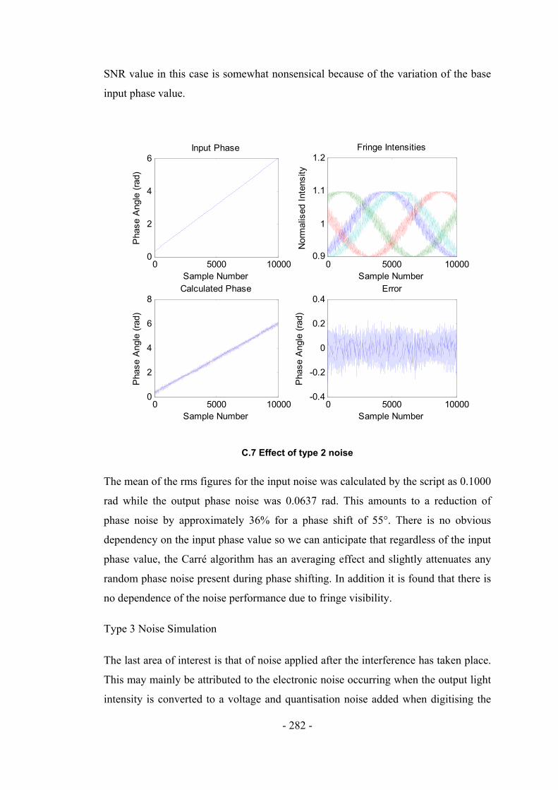
- 282 -
SNR value in this case is somewhat nonsensical because of the variation of the base
input phase value.
0 5000 100000
2
4
6Input Phase
Pha
se A
ngle
(rad
)
Sample Number0 5000 10000
0.9
1
1.1
1.2Fringe Intensities
Nor
mal
ised
Inte
nsity
Sample Number
0 5000 100000
2
4
6
8Calculated Phase
Sample Number
Pha
se A
ngle
(rad
)
0 5000 10000-0.4
-0.2
0
0.2
0.4Error
Sample Number
Pha
se A
ngle
(rad
)
C.7 Effect of type 2 noise
The mean of the rms figures for the input noise was calculated by the script as 0.1000
rad while the output phase noise was 0.0637 rad. This amounts to a reduction of
phase noise by approximately 36% for a phase shift of 55°. There is no obvious
dependency on the input phase value so we can anticipate that regardless of the input
phase value, the Carré algorithm has an averaging effect and slightly attenuates any
random phase noise present during phase shifting. In addition it is found that there is
no dependence of the noise performance due to fringe visibility.
Type 3 Noise Simulation
The last area of interest is that of noise applied after the interference has taken place.
This may mainly be attributed to the electronic noise occurring when the output light
intensity is converted to a voltage and quantisation noise added when digitising the
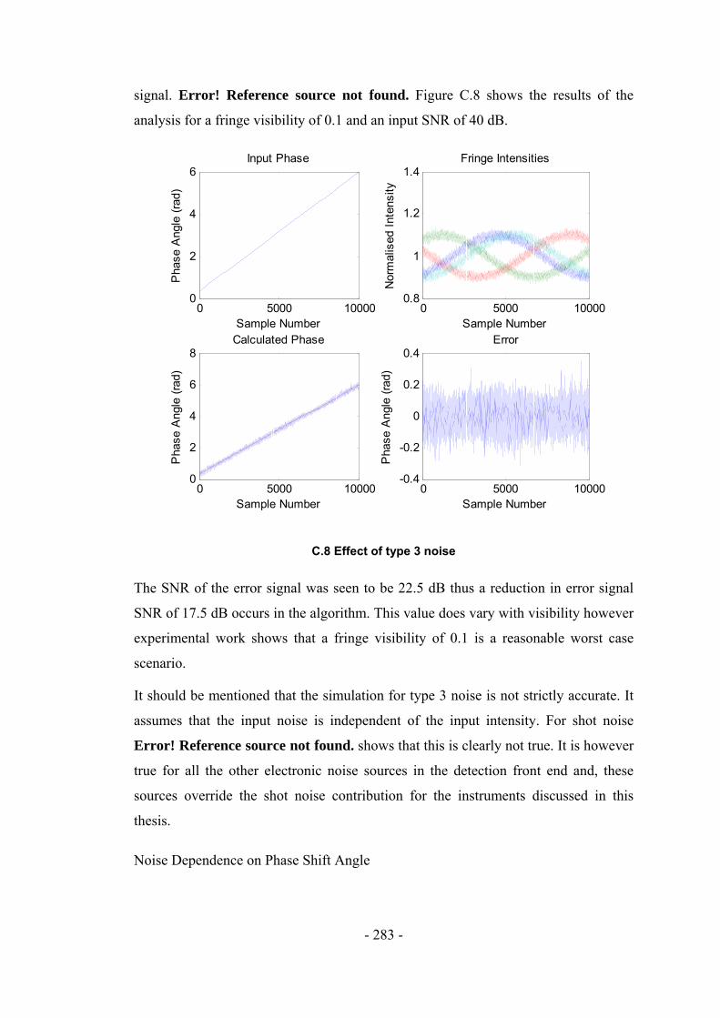
- 283 -
signal. Error! Reference source not found. Figure C.8 shows the results of the
analysis for a fringe visibility of 0.1 and an input SNR of 40 dB.
0 5000 100000
2
4
6Input Phase
Pha
se A
ngle
(rad
)
Sample Number0 5000 10000
0.8
1
1.2
1.4Fringe Intensities
Nor
mal
ised
Inte
nsity
Sample Number
0 5000 100000
2
4
6
8Calculated Phase
Sample Number
Pha
se A
ngle
(rad
)
0 5000 10000-0.4
-0.2
0
0.2
0.4Error
Sample Number
Pha
se A
ngle
(rad
)
C.8 Effect of type 3 noise
The SNR of the error signal was seen to be 22.5 dB thus a reduction in error signal
SNR of 17.5 dB occurs in the algorithm. This value does vary with visibility however
experimental work shows that a fringe visibility of 0.1 is a reasonable worst case
scenario.
It should be mentioned that the simulation for type 3 noise is not strictly accurate. It
assumes that the input noise is independent of the input intensity. For shot noise
Error! Reference source not found. shows that this is clearly not true. It is however
true for all the other electronic noise sources in the detection front end and, these
sources override the shot noise contribution for the instruments discussed in this
thesis.
Noise Dependence on Phase Shift Angle
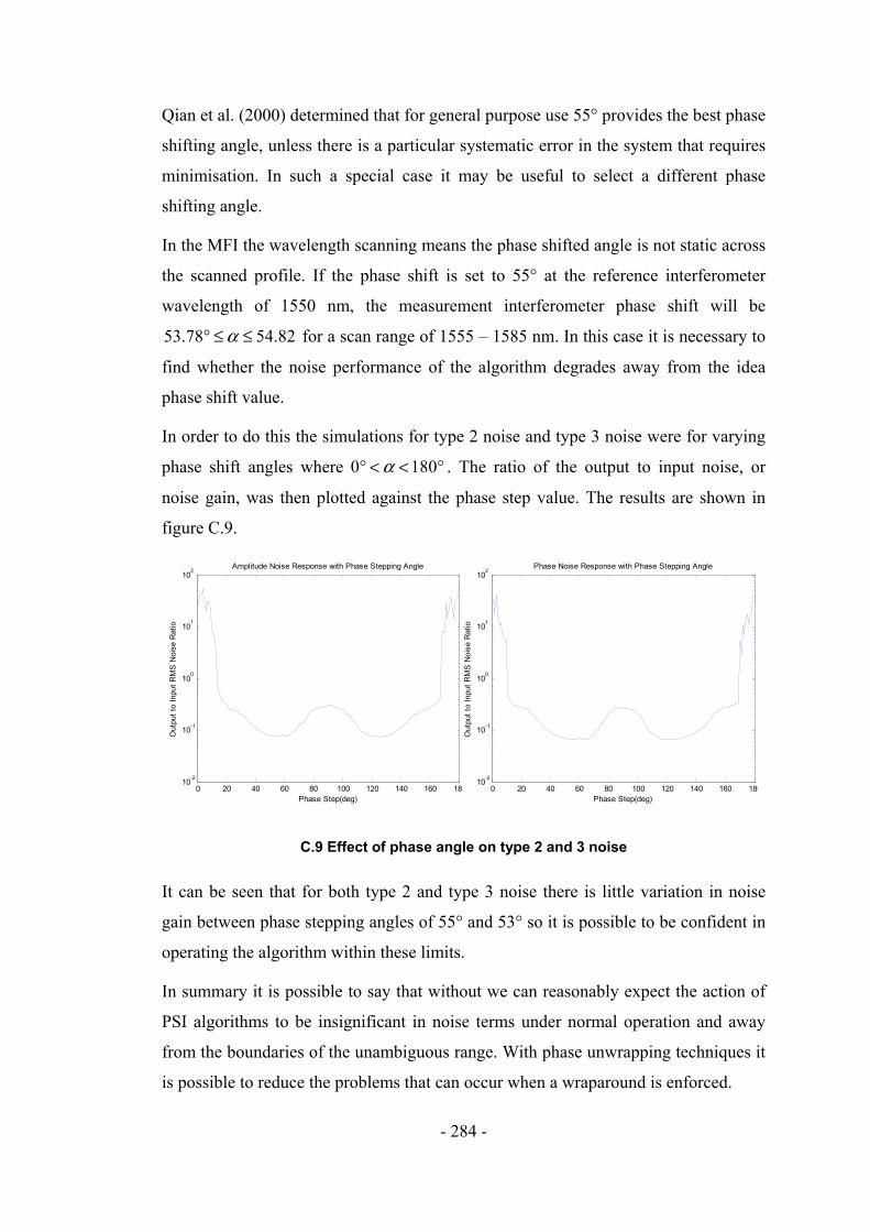
- 284 -
Qian et al. (2000) determined that for general purpose use 55° provides the best phase
shifting angle, unless there is a particular systematic error in the system that requires
minimisation. In such a special case it may be useful to select a different phase
shifting angle.
In the MFI the wavelength scanning means the phase shifted angle is not static across
the scanned profile. If the phase shift is set to 55° at the reference interferometer
wavelength of 1550 nm, the measurement interferometer phase shift will be
53.78 54.82α° ≤ ≤ for a scan range of 1555 – 1585 nm. In this case it is necessary to
find whether the noise performance of the algorithm degrades away from the idea
phase shift value.
In order to do this the simulations for type 2 noise and type 3 noise were for varying
phase shift angles where 0 180α° < < ° . The ratio of the output to input noise, or
noise gain, was then plotted against the phase step value. The results are shown in
figure C.9.
0 20 40 60 80 100 120 140 160 18010-2
10-1
100
101
102Amplitude Noise Response with Phase Stepping Angle
Phase Step(deg)
Out
put t
o In
put R
MS
Noi
se R
atio
0 20 40 60 80 100 120 140 160 18010-2
10-1
100
101
102Phase Noise Response with Phase Stepping Angle
Phase Step(deg)
Out
put t
o In
put R
MS
Noi
se R
atio
C.9 Effect of phase angle on type 2 and 3 noise
It can be seen that for both type 2 and type 3 noise there is little variation in noise
gain between phase stepping angles of 55° and 53° so it is possible to be confident in
operating the algorithm within these limits.
In summary it is possible to say that without we can reasonably expect the action of
PSI algorithms to be insignificant in noise terms under normal operation and away
from the boundaries of the unambiguous range. With phase unwrapping techniques it
is possible to reduce the problems that can occur when a wraparound is enforced.

- 285 -
D Matlab Scripts
D.1 Matlab Script for LF356 Transimpedance Analysis
% This script describes the response of a LF356 transimpedance amplifier. % Component Values go here Rd = 5e9 % Diode shunt resistance Cd = 1e-12 % Diode parasitic capacitance Cin =3e-12 % Opamp input capacitance Rf = 50e3 % Feedback resistance Cf = 10e-12 % Feedback capacitance Cp = Cd + Cin % Total parasitic capacitance % Aol is approximated by a 1st order LPF with a break frequency of 28Hz and 20dB/decade roll off. Aol = 1.77828e5 * tf([1] , [(1/(45*pi)) 1]) ; % Open loop voltage gain LF356 (105 dB, GBW 4 Mhz) % Calculate the shunt complex impedance at the input due to diode % characteristics and parasitic capacitances. Zsh = tf( [Rd] , [(Cp*Rd) 1]); % Calculate feedback complex impedance for the transimpedance amplifier. This % provides the response roll off Zf = tf( [Rf] , [(Cf*Rf) 1]); % Here we calculate the feedback fraction, beta and the resulting CL % voltage gain and transimpedance beta = 1 / (1 + (Zf / Zsh)); % Feedback Fraction, Beta Acl = Aol / (1 + (beta * Aol)); % Closed Loop Gain trans = (Aol * Zf ) / (1 + Aol + (Zf / Zsh)); % Transimpedance %%%%%%%%%%%%%%%%%%%%%%%%%%%%%%%%%%%%%%%%%%%%%%%%%%%%% % Determine transimpedance values in numeric terms [MAGtrans,PHtrans,Wtrans]=bode(trans,1,1e8); MAGtrans = MAGtrans(:); PHtrans = MAGtrans(:); Ftrans = Wtrans./ (2*pi) % Graphical Routines go here figure(1) step(trans); % Plot Step Response figure(2) subplot(2,2,1); % Plot Op Amp Open Loop Gain bode(Aol,1,1e8) title('Open Loop Gain, Aol') xlabel('Frequency (Hz)') ylabel('Voltage Gain (dB)') %axis([10 1e7 0 130]) subplot(2,2,2); % Plot Closed Loop Voltage Gain bode(Acl,1 1e8) title('Closed Loop Voltage Gain, Acl') xlabel('Frequency (Hz)') ylabel('Voltage Gain (dB)') %axis([10 1e7 0.1 10]) subplot(2,2,3); % Plot Transimpedance (dB) bode(trans,1,1e8) title('Transimpedance, (dB)') xlabel('Frequency (Hz)') ylabel('Current Gain (dB)') %axis([10 1e7 0 130]) subplot(2,2,4); % Plot Transimpedance (ohms) semilogx (Ftrans,MAGtrans); title('Transimpedance') xlabel('Frequency (Hz)') ylabel('Current Gain (Iph/V)') axis([10 1e7 0 Rf])

- 286 -
D.2 Matlab Script for THS4062 Transimpedance Analysis
% This script describes the response of a THS4062 transimpedance amplifier. % Component Values go here Rd = 5e9 % Diode shunt resistance Cd = 1e-12 % Diode parasitic capacitance Cin =3e-12 % Opamp input capacitance Rf = 100e3 % Feedback resistance Cf = 10e-12 % Feedback capacitance Cp = Cd + Cin % Total parasitic capacitance % Aol is approximated by a 1st order LPF with a break frequency of 28Hz and 20dB/decade roll off. Aol = 1.77828e5 * tf([1] , [(1/(45*pi)) 1]) ; % Open loop voltage gain LF356 (105 dB, GBW 4 Mhz) % Calculate the shunt complex impedance at the input due to diode % characteristics and parasitic capacitances. Zsh = tf( [Rd] , [(Cp*Rd) 1]); % Calculate feedback complex impedance for the transimpedance amplifier. This % provides the response roll off Zf = tf( [Rf] , [(Cf*Rf) 1]); % Here we calculate the feedback fraction, beta and the resulting CL % voltage gain and transimpedance beta = 1 / (1 + (Zf / Zsh)); % Feedback Fraction, Beta Acl = Aol / (1 + (beta * Aol)); % Closed Loop Gain trans = (Aol * Zf ) / (1 + Aol + (Zf / Zsh)); % Transimpedance %%%%%%%%%%%%%%%%%%%%%%%%%%%%%%%%%%%%%%%%%%%%%%%%%%%%% % Determine transimpedance values in numeric terms [MAGtrans,PHtrans,Wtrans]=bode(trans,1,1e8); MAGtrans = MAGtrans(:); PHtrans = MAGtrans(:); Ftrans = Wtrans./ (2*pi); % Graphical Routines go here figure(1) step(trans); % Plot Step Response figure(2) subplot(2,2,1); % Plot Op Amp Open Loop Gain bodemag(Aol,1,1e8) title('Open Loop Gain, Aol') %xlabel('Frequency (Hz)') %ylabel('Voltage Gain (dB)') %axis([10 1e7 0 130]) subplot(2,2,2); % Plot Closed Loop Voltage Gain bodemag(Acl,1 1e8) title('Closed Loop Voltage Gain, Acl') %xlabel('Frequency (Hz)') %ylabel('Voltage Gain (dB)') %axis([10 1e7 0.1 10]) subplot(2,2,3); % Plot Transimpedance (dB) bodemag(trans,1,1e8) title('Transimpedance, (dB)') %xlabel('Frequency (Hz)') %ylabel('Current Gain (dB)') %axis([10 1e7 0 130]) subplot(2,2,4); % Plot Transimpedance (ohms) semilogx (Ftrans,MAGtrans); title('Transimpedance') xlabel('Frequency (Hz)') ylabel('Transimpedance (ohms)') axis([10 1e7 0 Rf]) grid on; %[MAG,PHASE] = BODE(Aol,(4e6)*(2*pi)); %MAG = 20*log10(MAG)

- 287 -
D.3 Matlab Script for Disturbance Rejection Analysis
% Script to simulate the behaviour of the closed loop disturbance % rejection method employed on the MFI. % Haydn Martin 1/4/2008 clear all; % PI Parallel Controller Definition Kp = [0 0.001 0.01 0.1 1] % Prop Gain Matrix Ki = [1e3 2e3 3e3 4e3 5.75e3] % Integrator Gain Matrix %Ki = 5.75e3 % Integrator Gain % Setup up SISO transfer function matrix with varying Kp and Ki values for n=1:5, for j=1:5, %Gc(1,1,j,n) = Kp(j) + tf(Ki(n) , [1 0]); % Integrator Transfer Function Gc(1,1,j,n) = tf([Kp(j) Ki(n)] , [1 0]); % Integrator Transfer Function end end % Modelling of PZT response k = 18.67e6 % Stiffness (N/m) m = 1e-3 % Mass (kg) Fres = 22e3 % Unloaded piezo resonance (Hz) m0 = k/((2*pi*Fres)^2) % Calculate unloaded mass meff = m + m0 % Effective mass includes PZT unloaded mass + load mass Wn = sqrt(k/meff) % Calculate resonant frequency (rad) from stiffness and mass Q = 5 % Quality factor. Decreases with increased damping Fn = Wn/(2*pi) % Resonant frequency (Hz) %Q=[1 2 5 10 20] %for n=1:5, %Gpzt(1,1,1,n) = tf(Wn^2, [1 (Wn./Q(n)) Wn^2]); % PZT Response Model %end Gpzt = tf(Wn^2, [1 (Wn/Q) Wn^2]); %%%%%%%%%%%%%%%%%%%%%%%%%%%%%%%%%%%%%%%%%%%%%%%%%%%%%%%%%%%%%%%%%%%%%%% % Conversion Gains of the Photodiode frontend and the interferometer Kpd = 150e3 Kif = 1/50e3 %%%%%%%%%%%%%%%%%%%%%%%%%%%%%%%%%%%%%%%%%%%%%%%%%%%%%%%%%%%%%%%%%%%%%%% Gs = Gc*Gpzt*Kif*Kpd; % Calculate openloop transfer function CLTF = feedback(Gs,1); % Calculate closed loop transfer function sens = Kif*Kpd/(1 + (Kif*Kpd*Gc*Gpzt)); % Disturbance sensitivity function %ltiview(pzt,PI,closed) % STUDY OF INTEGRATION GAIN VARIATION % Tests for stability are CL Step Response, Open Loop Bode and Open Loop Nichols Psel = 4; % Select Kp array number for graphing figure(1) step(CLTF(:,:,Psel,1),'b',CLTF(:,:,Psel,2),'k',CLTF(:,:,Psel,3),'r',CLTF(:,:,Psel,4),'m',CLTF(:,:,Psel,5),'g') grid on; legend('Ki=1 kHz','Ki=2 kHz','Ki=3 kHz','Ki=4 kHz','Ki=5.75 kHz'); title('Kp=0.1') axis([0 7e-3 0 1.2]) figure(2) bode(Gs(:,:,Psel,1),'b',Gs(:,:,Psel,2),'k',Gs(:,:,Psel,3),'r',Gs(:,:,Psel,4),'m',Gs(:,:,Psel,5),'g',1,10e5) grid on legend('Ki=1 kHz','Ki=2 kHz','Ki=3 kHz','Ki=4 kHz','Ki=5.75 kHz'); title('Kp=0.1') axis auto figure(3) nichols(Gs(:,:,Psel,1),'b',Gs(:,:,Psel,2),'k',Gs(:,:,Psel,3),'r',Gs(:,:,Psel,4),'m',Gs(:,:,Psel,5),'g',1,10e5) axis tight; legend('Ki=1 kHz','Ki=2 kHz','Ki=3 kHz','Ki=4 kHz','Ki=5.75 kHz'); title('Kp=0.1') axis auto % Peformance Study is Sensitivity Bode figure(4) bode(sens(:,:,Psel,1),'b',sens(:,:,Psel,2),'k',sens(:,:,Psel,3),'r',sens(:,:,Psel,4),'m',sens(:,:,Psel,5),'g',1,10e5) grid on legend('Ki=1 kHz','Ki=2 kHz','Ki=3 kHz','Ki=4 kHz','Ki=5.75 kHz'); title('Kp=0.1') axis auto % STUDY OF PROPORTIONAL GAIN VARIATION Isel = 3; % Select Ki array number for graphing

- 288 -
figure(5) step(CLTF(:,:,1,Isel),'b',CLTF(:,:,2,Isel),'k',CLTF(:,:,3,Isel),'r',CLTF(:,:,4,Isel),'m',CLTF(:,:,5,Isel),'g'); axis tight; grid on legend('Kp=0','Kp=0.001','Kp=0.01','Kp=0.1','Kp=1'); title('Kp=3 kHz') axis auto figure(6) bode(Gs(:,:,1,Isel),'b',Gs(:,:,2,Isel),'k',Gs(:,:,3,Isel),'r',Gs(:,:,4,Isel),'m',Gs(:,:,5,Isel),'g',1,10e5); axis tight; grid on title('Kp=3 kHz') legend('Kp=0','Kp=0.001','Kp=0.01','Kp=0.1','Kp=1'); axis auto figure(7) nichols(Gs(:,:,1,Isel),'b',Gs(:,:,2,Isel),'k',Gs(:,:,3,Isel),'r',Gs(:,:,4,Isel),'m',Gs(:,:,5,Isel),'g',1,10e5); title('Kp=3 kHz') legend('Kp=0','Kp=0.001','Kp=0.01','Kp=0.1','Kp=1'); axis auto figure(7) nichols(sens(:,:,1,Isel),'b',sens(:,:,2,Isel),'k',sens(:,:,3,Isel),'r',sens(:,:,4,Isel),'m',sens(:,:,5,Isel),'g',1,10e5); title('Kp=3 kHz') legend('Kp=0','Kp=0.001','Kp=0.01','Kp=0.1','Kp=1'); axis auto % Peformance Study is Sensitivity Bode figure(8) bode(sens(:,:,1,Isel),'b',sens(:,:,2,Isel),'k',sens(:,:,3,Isel),'r',sens(:,:,4,Isel),'m',sens(:,:,5,Isel),'g',1,10e5); grid on title('Kp=3 kHz') legend('Kp=0','Kp=0.001','Kp=0.01','Kp=0.1','Kp=1'); axis auto figure(9) step(Gpzt); grid on

- 289 -
D.4 Matlab Script for Transimpedance Amplifier Noise
% This script describes the response of a transimpedance amplifier. clear all; % Universal Constants/Settings kB = 1.3806503e-23; % Boltzmann constant, m2 kg s-2 K-1 T = 300; % Operating temperature, K elec = 1.60217646e-19; % Charge on an electron, Coulombs i_ph = 40e-6; % DC Photocurrent produced Vbias = 5; Rf = 100e3; % Feedback resistance Rd = 5e9; % Diode shunt resistance Cd = 1e-12; % Diode parasitic capacitance f = logspace(0.1,9,1000); % Setup frequency array for integration frad = f*2*pi; % LF356 Component Values go here Cin =3e-12; % Opamp input capacitance Cf = 1.3e-12; % Feedback capacitance % Aol is approximated by a 1st order LPF with a break frequency of 28Hz and 20dB/decade roll off. Aol = 1.77828e5 * tf([1] , [(1/(45*pi)) 1]) ; % Open loop voltage gain LF356 (105 dB, GBW 4 Mhz) % Calculate the shunt complex impedance at the input due to diode % characteristics and parasitic capacitances. Cp = Cd + Cin; % Total parasitic capacitance Zsh = tf( [Rd] , [(Cp*Rd) 1]); % Calculate feedback complex impedance for the transimpedance amplifier. This % provides the response roll off Zf = tf( [Rf] , [(Cf*Rf) 1]); % Here we calculate the feedback fraction, beta and the resulting CL % voltage gain and transimpedance beta = 1 / (1 + (Zf / Zsh)); % Feedback Fraction, Beta Acl = Aol / (1 + (beta * Aol)); % Closed Loop Gain trans = (Aol * Zf ) / (1 + Aol + (Zf / Zsh)); % Transimpedance trans1=trans; %%%%%%%%%%%%%%%%%%%%%%%%%%%%%%%%%%%%%%%%%%%%%%%%%%%%%% % Define white noise sources Vn_amp = (15e-9) ^ 2 % LF 356 amplifier voltage noise (white), V^2/Hz In_shunt = (4*kB*T/Rd) % Johnson current noise from shunt resistance, A^2/Hz In_feed = (4*kB*T/Rf) % Johnson current noise from feedback resistance, A^2/Hz In_photo = 2 * elec * i_ph % Shot noise associated with photo-current, A^2/Hz In_dark = 2 * elec * (Vbias/Rd) % Shot noise associated with dark current, A^2/Hz In_amp = (0.01e-12) ^2 % Amplifer current noise, this is taken as flatband A^2/Hz) In_total = In_shunt + In_dark + In_photo + In_feed + In_amp % Total current spectral density, A^2/Hz % Calculate Power Spectral Densities In_PSD = trans * In_total; % Current noise PSD V/root Hz Vn_PSD = Acl * Vn_amp; % Voltage Noise PSD V/root Hz DC_output = i_ph * Rf; % Integrate Power Spectral Densities to obtain RMS noise voltage [Vn]= bode(Vn_PSD,frad); Vn=squeeze(Vn); rootVn=1e9*sqrt(Vn); [In]= bode(In_PSD,frad); In=squeeze(In); rootIn=1e9*sqrt(In); Vn_meansq = sqrt(trapz(f,Vn)) In_meansq = sqrt(trapz(f,In)) rms_total = sqrt(Vn_meansq + In_meansq) SNR = 20*log(DC_output/rms_total) % TDS4062 Specifications go here Cin = 2e-12 ; % Opamp input capacitance Cf = 0.3e-12; % Feedback capacitance % Aol is approximated by a 1st order LPF with a break frequency of 28Hz and 20dB/decade roll off. Aol = 15849 * tf([1] , [(1/(28274)) 1]) ; % Open loop voltage gain LF356 (105 dB, GBW 4 Mhz) % Calculate the shunt complex impedance at the input due to diode % characteristics and parasitic capacitances. Cp = Cd + Cin; % Total parasitic capacitance Zsh = tf( [Rd] , [(Cp*Rd) 1]); % Calculate feedback complex impedance for the transimpedance amplifier. This % provides the response roll off Zf = tf( [Rf] , [(Cf*Rf) 1]); % Here we calculate the feedback fraction, beta and the resulting CL % voltage gain and transimpedance beta = 1 / (1 + (Zf / Zsh)); % Feedback Fraction, Beta

- 290 -
Acl = Aol / (1 + (beta * Aol)); % Closed Loop Gain trans = (Aol * Zf ) / (1 + Aol + (Zf / Zsh)); % Transimpedance % Define white noise sources Vn_amp2 = (14.5e-9) ^ 2 % LF 356 amplifier voltage noise (white), V^2/Hz In_shunt2 = (4*kB*T/Rd) % Johnson current noise from shunt resistance, A^2/Hz In_feed2 = (4*kB*T/Rf) % Johnson current noise from feedback resistance, A^2/Hz In_photo2 = 2 * elec * i_ph % Shot noise associated with photo-current, A^2/Hz In_dark2 = 2 * elec * (Vbias/Rd) % Shot noise associated with dark current, A^2/Hz In_amp2 = (1.6e-12) ^2 % Amplifer current noise, this is taken as flatband A^2/Hz) In_total2 = In_shunt2 + In_dark2 + In_photo2 + In_feed2 + In_amp2 % Total current power spectral density, A^2/Hz % Calculate Power Spectral Densities In_PSD2 = trans * In_total2; % Current noise PSD V^2/Hz Vn_PSD2 = Acl * Vn_amp2; % Voltage Noise PSD V^2/Hz DC_output = i_ph * Rf; % Integrate Power Spectral Densities to obtain RMS noise voltage [Vn2]= bode(Vn_PSD2,frad); Vn2=squeeze(Vn2); rootVn2=1e9*sqrt(Vn2); [In2]= bode(In_PSD2,frad); In2=squeeze(In2); rootIn2=1e9*sqrt(In2); Vn_meansq2 = sqrt(trapz(f,Vn2)) In_meansq2 = sqrt(trapz(f,In2)) % Calculate summed RMS noise at output rms_total2 = sqrt(Vn_meansq2 + In_meansq2) SNR2 = 20*log(DC_output/rms_total2) % Graphical Routines go here figure(1) bode(trans1,'b',trans,'r',2*pi*1e4,2*pi*1e7); title('Transimpedance') legend('LF356','THS4062'); grid on; figure(2) subplot(2,1,1) semilogx(f,rootIn,'b',f,rootIn2,'r') title('Current Noise Spectral Density') ylabel('V/sqrt(Hz)') xlabel('Frequency (Hz)') grid on; axis tight; legend('LF356','THS4062'); subplot(2,1,2) semilogx(f,rootVn,'b',f,rootVn2,'r') title('Voltage Noise Spectral Density') axis tight; legend('LF356','THS4062'); ylabel('V/sqrt(Hz)') xlabel('Frequency (Hz)') grid on;

- 291 -
D.5 Matlab Script for Disturbance Rejection Analysis Rapid Phase
Shifting Method
% Matlab Script for Control loop analysis of the Rapid Phase Shifting Method % Haydn Martin 6/5/09 clear all; % PI Parallel Controller Definition Kp = [0.001 0.01 0.1 0.3 0.5] % Prop Gain Matrix Ki = [10e-6 20e-6 27e-6 100e-6 200e-6] % Integrator Gain Matrix % Integrator Gain Ts = 27e-6 % Sampling Interval % Setup up SISO transfer function matrix with varying Kp and Ki values for n=1:5, for j=1:5, Gc(1,1,j,n) = Kp(j) * (1 + tf([Ts 0],[Ki(n) -Ki(n)],Ts)); % Integrator Transfer Function end end %%%%%%%%%%%%%%%%%%%%%%%%%%%%%%%%%%%%%%%%%%%%%%%%%%%%%%%%%%%%%%%%%%%%%%% Gd = tf([1],[1 0],Ts); Gs = Gc * Gd; %%%%%%%%%%%%%%%%%%%%%%%%%%%%%%%%%%%%%%%%%%%%%%%%%%%%%%%%%%%%%%%%%%%%%%% CLTF = feedback(Gs,1); % Calculate closed loop transfer function sens = Gd/(1+ (Gc*Gd*Gd)); % Disturbance sensitivity function % STUDY OF INTEGRATION GAIN VARIATION % Tests for stability are CL Step Response, Open Loop Bode and Open Loop Nichols Psel = 4; % Select Kp array number for graphing figure(1) step(CLTF(:,:,Psel,1),'b',CLTF(:,:,Psel,2),'k',CLTF(:,:,Psel,3),'r',CLTF(:,:,Psel,4),'m',CLTF(:,:,Psel,5),'g') grid on; legend('Ki=10 us','Ki=20 us','Ki=27 us','Ki=100 us','Ki=200 us'); title('Kp=0.3') axis([0 3e-3 0 1.2]) figure(2) bode(Gs(:,:,Psel,1),'b',Gs(:,:,Psel,2),'k',Gs(:,:,Psel,3),'r',Gs(:,:,Psel,4),'m',Gs(:,:,Psel,5),'g',1,10e5) grid on legend('Ki=1 kHz','Ki=2 kHz','Ki=3 kHz','Ki=4 kHz','Ki=5.75 kHz'); title('Kp=0.1') axis auto figure(3) nichols(Gs(:,:,Psel,1),'b',Gs(:,:,Psel,2),'k',Gs(:,:,Psel,3),'r',Gs(:,:,Psel,4),'m',Gs(:,:,Psel,5),'g',1,10e5) axis tight; legend('Ki=1 kHz','Ki=2 kHz','Ki=3 kHz','Ki=4 kHz','Ki=5.75 kHz'); title('Kp=0.1') axis auto % Peformance Study is Sensitivity Bode figure(4) bode(sens(:,:,Psel,1),'b',sens(:,:,Psel,2),'k',sens(:,:,Psel,3),'r',sens(:,:,Psel,4),'m',sens(:,:,Psel,5),'g',1,10e5) grid on legend('Ki=10 us','Ki=20 us','Ki=27 us','Ki=100 us','Ki=200 us'); title('Kp=0.3') axis auto % STUDY OF PROPORTIONAL GAIN VARIATION Isel = 3; % Select Ki array number for graphing figure(5) step(CLTF(:,:,1,Isel),'b',CLTF(:,:,2,Isel),'k',CLTF(:,:,3,Isel),'r',CLTF(:,:,4,Isel),'m',CLTF(:,:,5,Isel),'g'); axis tight; grid on legend('Kp=0','Kp=0.001','Kp=0.01','Kp=0.1','Kp=1'); title('Kp=3 kHz') axis auto figure(6) bode(Gs(:,:,1,Isel),'b',Gs(:,:,2,Isel),'k',Gs(:,:,3,Isel),'r',Gs(:,:,4,Isel),'m',Gs(:,:,5,Isel),'g',1,10e5); axis tight; grid on title('Kp=3 kHz') legend('Kp=0','Kp=0.001','Kp=0.01','Kp=0.1','Kp=1'); axis auto figure(7)

- 292 -
nichols(Gs(:,:,1,Isel),'b',Gs(:,:,2,Isel),'k',Gs(:,:,3,Isel),'r',Gs(:,:,4,Isel),'m',Gs(:,:,5,Isel),'g',1,10e5); title('Kp=3 kHz') legend('Kp=0','Kp=0.001','Kp=0.01','Kp=0.1','Kp=1'); axis auto figure(7) nichols(sens(:,:,1,Isel),'b',sens(:,:,2,Isel),'k',sens(:,:,3,Isel),'r',sens(:,:,4,Isel),'m',sens(:,:,5,Isel),'g',1,10e5); title('Kp=3 kHz') legend('Kp=0','Kp=0.001','Kp=0.01','Kp=0.1','Kp=1'); axis auto % Peformance Study is Sensitivity Bode figure(8) bode(sens(:,:,1,Isel),'b',sens(:,:,2,Isel),'k',sens(:,:,3,Isel),'r',sens(:,:,4,Isel),'m',sens(:,:,5,Isel),'g',1,10e5); grid on title('Kp=3 kHz') legend('Kp=0','Kp=0.001','Kp=0.01','Kp=0.1','Kp=1'); axis auto

- 293 -
E TMS320F2812 DSP C Code
E.1 Introduction
This code listing gives all the generated code for the V2 MFI as described in chapter
7. Any functions or header files not listed are part of the supplied libraries from
Texas Instruments. This includes specifically the IQmathLib.h header file which
contain the function declarations for the IQmath floating point emulator used. Also
some of the supplied initialisation routines for the DSP and its peripherals are used
for the initial setup, with further parameter selection being done in this code listing.
• Overall the code listing is structured thus:
• Constant definitions
• Function declarations
• Variable initialisation
• DSP/peripheral initialisation
• Main loop
• Interrupt service routines (ISRs)
• General functions
• Peripheral setup functions
E.2 Code Description
The code is fully commented throughout but it is of benefit to discuss some of the
user changeable functionality. Any parameter changes are accessed through the
constant definitions so a brief description is given here.
SCHWIDER
If this constant is defined the Schwider algorithm is used to calculate the feedback
phase. If commented out the Carré algorithm will be used instead.
INVERT

- 294 -
Inverts the output voltage signal to the DAC if defined. Useful only for some
debugging purposes.
Fs
Defines the sample rate for the control loop. Note that this is the sample rate for the
calculated phase feedback, not the individual phase shifts. It is used for calculating
control loop parameters.
KC
Proportional gain term used in the control algorithm.
Ti
Integration time constant (reciprocal of integration gain) used in the control
algorithm.
Defines the conversion gain for calculating the 16 bit value required to provide a 2π
phase shift by the EOPM.
ULIM and LIM
DAC upper and lower limits, the control algorithm resets automatically if either of
these limits is exceeded. Set for a 16 bit DAC.
DELAY
Sets the delay time for recording calculated phase data to the buffer. The value sets
the number of times the phase is calculated before a value is committed to the buffer.
Essentially the calculated phase is decimated before storage; a value of 40 provides
an approximate phase buffer length of around 1sec (40 X 1000 values at 27 μs
period).
WAIT
The intensity oscillation experienced using when the HP8168F tuneable laser is
wavelength shifted means that an appropriate settling time needs to be allowed for
before beginning intensity recording. This value controls a simple delay loop; a value
of 71 10× provides approximately 1 second of delay.
SETTLE

- 295 -
This defines the delay from the initial beginning of the measurement cycle to the
recording of intensity data. At the start up of the measurement cycle the action of the
control loop causes a transient as it pulls the interferometer from its free running
phase and into quadrature. The delay is necessary to ensure the intensity data is not
recorded until the transient settles. It only effects the first measurement point taken.
POINTMAX
Defines the number of points to be taken during the measurement cycle.
AVERAGEMAX
Defines the number of intensity measurement sets to be taken on a single point. This
is a noise reduction feature.
PBUFZ
Sets the buffer size for the calculated phase storage. Ultimately restricted by the DSP
on board memory.
IBUFZ
Sets the buffer size for the measured intensity value storage. This should be 5 times
the size of PBUFZ for Schwider algorithm use and 4 times for Carré type shifting.
CONTROL
If defined this enables the control loop. The control loop may be disabled by
commenting out the definition.

- 296 -
E.3 D3 DSP Code Listing for Rapid Phase Shifting MFI
1 //########################################################################### // // FILE: fastPI.c V4.7 // 5 // Haydn Martin 07/4/2009 // // // CHANGES: // 10 // Added dual step array for using both EOPM scales // // // ASSUMPTIONS: // 15 // This program requires the DSP281x V1.00 header files. // As supplied, this project is configured for "boot to H0" operation. // // Make sure the CPU clock speed is properly defined in // DSP281x_Examples.h before compiling this example. 20 // // Connect signals to be converted to: // // REF = AD0 // MEAS= BD0 25 // // DESCRIPTION: // // This example sets up the PLL in x10/2 mode, divides SYSCLKOUT // by six to reach a 25Mhz HSPCLK (assuming a 30Mhz XCLKIN). The 30 // clock divider in the ADC is not used so that the ADC will see // the 25Mhz on the HSPCLK. The EVA timer 1 clock period is set // to yield a 284 kHz sample rate. Overflow interrupt is enabled // and the EVA is setup to provide ADC SOC signal upon interrupt. // 35 // A series format PI controller is implemented with IQmath and is // executed during the ADC_ISR after sample conversion takes place. // Parameters may be changed using the #defines. // // Phase stepping is performed, with the phase shift values being 40 // defined in the p_val array. The control loop operates throughout. // // SPI interface is implemented with 10 MHz bitrate, providing 16 bit // update in 2us. Total time required for DAC update + settling is 3.5 us. // 45 // Talkthru option is available to pass sampled inpt directly to the ADC // (scaled) for debugging purposes. // // // 50 // // #include "DSP281x_Device.h" // DSP281x Headerfile Include File #include "DSP281x_Examples.h" // DSP281x Examples Include File #include "float.h" 55 #define GLOBAL_Q 16 // Defines global Q-format for IQmath functions #include "IQmathLib.h" // For IQmath functions #define PI 3.141592654 60 // *********************************************************************** // User definable values #define SCHWIDER // Use SCHWIDER 5 step algorithm. Comment out to use Carré 65 #define INVERT // Invert output to DAC #define Fs 37.037e3 // Setup samplerate here 70 #define KC 0.3 // Gain//0.1 #define Ti 1/Fs // Integration time constant //#define Ti 1e-5 // Integration time constant 75 #define PROP 2206.593 // EOPM -BLUE X3 Radian to radian scale factor //#define PROP 3502.73 // EOPM -ORANGE X1 Radian to radian scale factor (reduced range)

- 297 -
//#define PROP 6600.73 // EOPM -ORANGE X1 Radian to radian scale factor (reduced range) #define ULIM 32767 // DAC upper write limit 80 #define LLIM -32767 // DAC lower write limit #define DELAY 40 // Delay value for phase buffer. 1 sec = 40 //#define WAIT 15000000 // Wait for TLS intensity to settle after move 1 sec = 1e7 85 //#define WAIT 10000000 // Wait for TLS intensity to settle after move #define WAIT 100000 // Wait for TLS intensity to settle after move #define SETTLE 300000 // Number of phase shift cycles to wait before recording intensity #define POINTMAX 100 // Number of profile points taken 90 #define AVERAGEMAX 8 // Number of measurements taken for each point for averaging #define PBUFSZ 1000 // Calculated phase buffer size #define IBUFSZ 5000 // Calculated intensity buffer size 95 #define CONTROL // Enable Control loop //************************************************************************ 100 // Calculate the weighting coefficients for PI control #define K0 KC * (1 + (1/(Fs * Ti))) // K0 applied to current error, e0 #define K1 -1 * KC // K1 applied to previous error, e1 105 #define RSHIFT SHIFT * (PI / 180) // Convert phase shift to rad long GlobalQ = GLOBAL_Q; // Needed for IQmath gel based debugging // Prototype statements for functions found within this file. 110 interrupt void adc_isr(void); // ADC conversion finished ISR interrupt void cpu_timer0_isr(void); // CPU Timer0 ISR interrupt void eva_t1_isr(void); // EVA timer1 overflow ISR 115 // Peripheral setup routines void spi_fifo_init(void); void adc_init(void); void eva_t1_init(void); 120 // Other routines _iq do_carre(_iq []); _iq do_schwider(_iq []); 125 _iq do_cntrl (_iq); void buffer_phase(_iq , Uint16); void buffer_intensity(int16 []); _iq get_intensityA(void); int16 get_intensityB(void); 130 _iq chk_wrap(_iq); _iq add_pshift(_iq); _iq get_pshift(void); void write_dac(_iq); void move_laser(void); 135 _iq e0=0, e1=0, c_val=0; // PI control variables // Define constants for arctan unwrapping in IQ format // Ensure the IQ format is the same as used in the unwrap algorithm 140 _iq pi = _IQ(PI) , twopi = _IQ(2 * PI); _iq halfpi = _IQ(PI/2), twothirdpi = _IQ(3 * PI/2); // Phase shift values in rad and stored in global q. 145 #ifndef SCHWIDER // This sets up buffer for Carré algorithm shifting #define SHIFT 55 // Set 55 deg phase shift for Carré 150 #define STEPS 4 // Set number of phase steps _iq p_val[STEPS] = _IQ(-3 * RSHIFT), _IQ(-1 * RSHIFT),_IQ(RSHIFT),_IQ(3 * RSHIFT); #endif //SCHWIDER 155 #ifdef SCHWIDER // This sets up for Schwider - Hariharan algorithm shifting #define SHIFT 90 // Set 90 deg phase shift for Schwider 5 Step 160 #define STEPS 5 // Set number of phase steps _iq p_val[STEPS] = _IQ(-2 * RSHIFT), _IQ(-1 * RSHIFT),_IQ(0),_IQ(1 * RSHIFT),_IQ(2 * RSHIFT); #endif //SCHWIDER 165 _iq phase_step = 0; // Stores prefetched phase step values _iq i_val_buf[STEPS] = 0; // Buffer to store current ref intensity values int16 m_val_buf[STEPS] = 0; // Buffer to store current meas intensity values 170 float phase_buf[PBUFSZ]=0; // Circular buffer to store calculated phase values int16 intensity_buf[IBUFSZ]=0; // Circular buffer to store intensity vales 175 Uint16 average = 0, points = 0; // Counter for averaging and points values

- 298 -
// Miscellaneous Vars 180 //_iq temp; // For general debug Uint32 h=0; // Loop variable for zeroing buffers main() 185 Uint16 LoopCount=0; // Loop variable for main do nothing loop InitSysCtrl(); EALLOW; // Enable write to protected registers 190 // Set HSPCLK to SYSCLKOUT / 6 (25Mhz assuming 150Mhz SYSCLKOUT) SysCtrlRegs.HISPCP.all = 0x3; // HSPCLK = SYSCLKOUT/6 195 // LOSPCP prescale register settings, set to give 150 Mhz (150/1) SysCtrlRegs.LOSPCP.all = 0x0000; //LSPCLK = SYSCLKOUT/1 EDIS; // Disable write to protected registers 200 // Step 2. Initialize GPIO: // This example function is found in the DSP281x_Gpio.c file and // illustrates how to set the GPIO to it's default state. 205 // InitGpio(); // Skipped for this example GpioDataRegs.GPBCLEAR.all = 0x101E; // Clear all GPIOB outputs to initialise EALLOW; // Enable write to protected registers. 210 GpioMuxRegs.GPFMUX.all=0x000F; // Select GPIOs to be SPI pins // Port F MUX - x000 0000 0000 1111 215 // Note here that masks are used so as only to write the bits we require GpioMuxRegs.GPFMUX.all&=0xBFFF; // Selects T1PWM and T2PWM as I/O pins // Port F MUX - x0xx xxxx xxxx xxxx 220 GpioMuxRegs.GPFDIR.all|=0x4000; // And set them all to outputs // Port F DIR - x1xx xxxx 11xx xxxx // The following sets PWM8:11 pins as output, for debugging purposes 225 GpioMuxRegs.GPBMUX.all&=0xEFE1; // Selects PWM8:11 and TCLKINB as I/O pins // Port B MUX - xxx0 xxxx xxx0 000x GpioMuxRegs.GPBDIR.all|=0x101E; // And set them all to outputs // Port B DIR - xxx1 xxxx xxx1 111x 230 GpioMuxRegs.GPBDIR.bit.GPIOB4 = 0; // Set GPIOB/PWM11 to INPUT GpioMuxRegs.GPBQUAL.bit.QUALPRD = 0x0F; // Set 32 x SYSCLKOUT debounce period on inputs 235 EDIS; GpioDataRegs.GPBCLEAR.bit.GPIOB3 = 1; // Reset PWM10 to initialise // Step 3. Clear all interrupts and initialize PIE vector table: 240 // Disable CPU interrupts. This ensures no false jumps when interrupt flags are SET DINT; // Initialize the PIE control registers to their default state. 245 // The default state is all PIE interrupts disabled and flags // are cleared. // This function is found in the DSP281x_PieCtrl.c file. InitPieCtrl(); 250 // Disable CPU interrupts and clear all CPU interrupt flags: IER = 0x0000; IFR = 0x0000; 255 // Initialize the PIE vector table with pointers to the shell Interrupt // Service Routines (ISR). // This will populate the entire table, even if the interrupt // is not used in this example. This is useful for debug purposes. 260 // The shell ISR routines are found in DSP281x_DefaultIsr.c. // This function is found in DSP281x_PieVect.c. InitPieVectTable(); 265 // Interrupts that are used in this example are re-mapped to // ISR functions found within this file. Address for eaxh interrupt routine is loaded into the // PIE vector table. The routine branches here when the interrupt origin has been determined. EALLOW; // This is needed to write to EALLOW protected register 270 PieVectTable.ADCINT = &adc_isr; // Enable PIE ADC complete interrupt PieVectTable.TINT0 = &cpu_timer0_isr;// Enable PIE cpu timer0 interrupt. PieVectTable.T1PINT = &eva_t1_isr; // Enable PIE eva timer 1 PERIOD interrupt. EDIS; // This is needed to disable write to EALLOW protected registe 275 // Step 4. Initialize all the Device Peripherals: // This function is found in DSP281x_InitPeripherals.c // InitPeripherals(); // Not required for this example 280 spi_fifo_init(); // Initialize the SPI only InitAdc(); // Init the ADC to a known state. Always run this first adc_init(); // Call our specific ADC setup routine

- 299 -
285 eva_t1_init(); // EVA setup routine to provide SOC for the ADC. InitCpuTimers(); // Initialize the Cpu Timers // Configure CPU-Timer 0 to interrupt every second: 290 // 150MHz CPU Freq, 1 second Period (in uSeconds) // This is used to flash the led on the EzDSP board to show // that the code is running and gives the main loop something to do. ConfigCpuTimer(&CpuTimer0, 150, 1000000); 295 //while(!GpioDataRegs.GPBDAT.bit.GPIOB4) // Wait for laser ready i.e. PWM11 is high // Step 6. Initialise intensity buffer to zero 300 while(h<IBUFSZ) intensity_buf[h]=0; 305 h++; 310 // Step 7. User specific code, enable interrupts: // Enable ADCINT in PIE 315 PieCtrlRegs.PIECRTL.bit.ENPIE = 1; // Enable the PIE block PieCtrlRegs.PIEIER1.bit.INTx6 = 1; // Enable PIE Group 1, INT 6, for ADC complete int PieCtrlRegs.PIEIER1.bit.INTx7 = 1; // Enable TINT0 in the PIE: Group 1 interrupt 7 320 PieCtrlRegs.PIEIER2.bit.INTx4 = 1; // Enable T1PINT EVA Timer1 Period Interrupt IER |= M_INT1; // Enable CPU INT1 which is connected to TIMER0 and AtoD IER |= M_INT2; // Enable CPU INT2 which is connected to T1PINT 325 EINT; // Enable Global interrupt INTM ERTM; // Enable Global realtime interrupt DBGM 330 SpiaRegs.SPITXBUF = 0; // Write 0 to DAC StartCpuTimer0(); // Start CPU timer to provde LED flash interrupts 335 // Wait forever for interrupt for(;;) LoopCount++; 340 if (average == AVERAGEMAX) // Test for complete averaging points taken points++; average = 0; // Reset counter and shift laser to the next p 345 move_laser(); 350 if (points == (POINTMAX-1)) points = 1; 355 /*************************************************************************************/ 360 // Interrupt Service Routines are contained within this section. /* This ISR executes when an ADC conversion is complete. PI controller 365 calculates the next required value to send to the DAC */ interrupt void adc_isr(void) 370 static Uint16 i=0; static _iq calc_phase , dc_phase; 375 GpioDataRegs.GPBSET.all = 0x0002; // SET PWM8 pin (Connect to scope) AdcRegs.ADCTRL2.bit.RST_SEQ1 = 1; // Reset Sequencer back to start (debug fix) switch (i- (STEPS - 1)) 380 case 0: // Final phase shift of sequence i_val_buf[i] = get_intensityA(); // Get averaged intensity value m_val_buf[i] = get_intensityB(); 385 i = 0; // Reset shift counter #ifndef SCHWIDER calc_phase = do_carre(i_val_buf); // Perform Carre Algorithm #endif 390 #ifdef SCHWIDER calc_phase = do_schwider(i_val_buf);// Perform Schwider-Hariharan Algorithm #endif 395

- 300 -
#ifdef CONTROL dc_phase = do_cntrl(calc_phase); // Apply PI control 400 #endif //CONTROL //phasestep = add_pshift(dc_phase); // Add next phase step 405 write_dac(dc_phase + phase_step); // Write to DAC 410 buffer_phase(calc_phase , DELAY); // Write current phase to buffer if (!GpioDataRegs.GPBDAT.bit.GPIOB3 && !GpioDataRegs.GPBDAT.bit.GPIOB4) 415 buffer_intensity(m_val_buf); break; default: // All other phase shifts 420 //phasestep = add_pshift(dc_phase); // Add next phase step write_dac(dc_phase + phase_step); // Write to DAC 425 i_val_buf[i] = get_intensityA(); // Get averaged intensity value m_val_buf[i] = get_intensityB(); // Get averaged intensity value i++; // Increment shift counter break; 430 // Here we provide for asymmetric timing of phase steps // Step 4 is timed for longer to allow the do_carre() and 435 // do_cntrl() to execute. // Extended period for Schwider is slightly shorter due to faster algorithm #ifndef SCHWIDER if (i == (STEPS -1)) EvaRegs.T1PR = 187; //Period = 7.5 us 440 else EvaRegs.T1PR = 125; // Period = 5us #endif //SCHWIDER #ifdef SCHWIDER if (i == (STEPS -1)) EvaRegs.T1PR = 170; // Period = 6.8 us 445 else EvaRegs.T1PR = 125; // Period = 5us #endif //SCHWIDER // if (!GpioDataRegs.GPBDAT.bit.GPIOB3) // If Laser is ready i.e. PWM10 is low 450 // Reinitialize for next ADC sequence AdcRegs.ADCST.bit.INT_SEQ1_CLR = 1; // Clear INT SEQ1 bit PieCtrlRegs.PIEACK.all |= PIEACK_GROUP1; // Acknowledge interrupt to PIE 455 GpioDataRegs.GPBCLEAR.all = 0x0002; // Clear PWM8 pin (Connect to scope) 460 // This ISR simply flashes the LED on the EZDsp once per second // Break points placed in this function allow the user to pull data // from the DSP at 1Hz intervals interrupt void cpu_timer0_isr(void) 465 static Uint16 ledtoggle=0; CpuTimer0.InterruptCount++; 470 ledtoggle ^= 1; GpioDataRegs.GPFTOGGLE.all = 0x4000; //Toggle ? pin (Connected to LED on EzDsp) // Acknowledge this interrupt to receive more interrupts from group 1 475 PieCtrlRegs.PIEACK.all = PIEACK_GROUP1; // Acknowledge Group 1 interrupts /* EVA timer 1 ISR provides the SOC signal for the ADC. Various counter values 480 can be set to provide different sampling rates. PWM10 (P8-33 ezdsp) is toggled at the start of the routine for debugging. This ISR does nothing useful. So may be disabled for more efficient running. 485 NB: The EVA timer1 period interrupt does NOT need to be enabled to provide the ADC SOC signal. */ 490 interrupt void eva_t1_isr(void) GpioDataRegs.GPBSET.all = 0x0002; //SET PWM8 pin (Connect to scope) 495 // Note: To be safe, use a mask value to write to the entire // EVAIFRA register. Writing to one bit will cause a read-modify-write // operation that may have the result of writing 1's to clear // bits other then those intended. 500 EvaRegs.EVAIFRA.all = 0x7FFF; // Clear T1PINT by writing here phase_step = get_pshift(); // Prefetch next phase shift value to save time.

- 301 -
505 EvaRegs.EVAIMRA.bit.T1PINT = 1; // Enable more interrupts from this timer // Acknowledge interrupt to receive more interrupts from PIE group 2 510 PieCtrlRegs.PIEACK.all = PIEACK_GROUP2; GpioDataRegs.GPBCLEAR.all = 0x0002; //RESET PWM8 pin (Connect to scope) 515 /*********************************************************************************/ // General functions are contained within this section. // PI control is carried out by this function 520 _iq do_cntrl(_iq phase) static _iq k0 = _IQ(K0); // K0= KC * (1 + (Ts / Ti)) 525 static _iq k1 = _IQ(K1); // K1 = -KC e0 = phase ^ 0xFFFFFFFF; // Calculate error value and shift to // the global Q-format. c_val +=_IQmpy(k0,e0); // Previous output add weighted e0 value 530 c_val +=_IQmpy(k1,e1); // Previous output add weighted e1 value e1 = e0; // Update error values return(c_val); 535 // This function performs an IQMath based implementation of the Carre Algorithm 540 _iq do_carre(_iq i_val[]) static _iq9 num0,num1,num2,num3,num4; // Variables for 1st part of Carre static _iq9 den, tmp, anum4, aden; // Variables for 2nd part of Carre 545 static _iq inter_phase; // Variables for 3rd part static Uint32 den_sign; 550 // GpioDataRegs.GPBSET.all = 0x0002; //SET PWM8 pin (Connect to scope) // Calculate Carre numerator num0 = i_val[1] - i_val[2]; // This is used later for arctan unwrap 555 num1 = _IQ9mpyI32(num0,3); num1 = num1 - i_val[0] - i_val[3]; 560 num2 = i_val[0] + i_val[1] - i_val[2] - i_val[3]; num3 = _IQ9mpy(num1,num2); anum4 = _IQ9abs(num3); 565 num4 = _IQ9sqrt(anum4); // Calculate Carre denominator 570 den = i_val[1]+i_val[2]-i_val[0]-i_val[3]; aden = _IQ9abs(den); 575 // Do Arctangent function tmp = _IQ9atan2(num4,aden); 580 inter_phase = tmp << (GLOBAL_Q-9); // Convert to GLOBALQ format // This section carries out sign tests on numerator and denominator and unwraps // the arctangent result correctly 585 if (num0==0) inter_phase = pi; // If numerator equal zero else den_sign = den & 0x80000000; // Get denominator sign 590 switch (num0 & 0x80000000) // Test numerator sign bit case (0): // numerator is +ve if (den_sign) inter_phase = pi - inter_phase; // denominator is -ve? else if (den == 0) inter_phase = halfpi; // denominator equals zero? 595 break; // Otherwise denominator is +ve, no action default : // Numerator is -ve if (den_sign) inter_phase += pi; // Denominator is -ve? else if (den == 0) inter_phase = twothirdpi; // Denominator equal zero? 600 else inter_phase = twopi - inter_phase; // Denominator must be +ve break; 605 // GpioDataRegs.GPBCLEAR.all = 0x0002; //Toggle PWM8 pin (Connect to scope) return(inter_phase-pi); 610 _iq do_schwider(_iq i_val[])

- 302 -
static _iq num, den; static _iq inter_phase; // Variables for 3rd part 615 // GpioDataRegs.GPBSET.all = 0x0002; //SET PWM8 pin (Connect to scope) 620 // Calculate Schwider numerator num = i_val[1] - i_val[3]; // This is used later for arctan unwrap 625 num = _IQmpyI32(num,2); // Calculate Schwider denominator 630 den = _IQmpyI32(i_val[2],2); den = den - i_val[4] - i_val[0]; // Do Arctangent function 635 inter_phase = _IQatan2(num,den); // GpioDataRegs.GPBCLEAR.all = 0x0002; //Toggle PWM8 pin (Connect to scope) 640 return(inter_phase); 645 // This routine updates a circular buffer with calculated phase values // The delay value essentially decimates the incoming phase values void buffer_phase(_iq phase, Uint16 delay) 650 static Uint16 i=0 , j=0; if (j>delay) // Store value if delay values // have already passed j=0; 655 phase_buf[i] = _IQtoF(phase); // Convert IQ to float for storage i++; if(i==PBUFSZ) i=0; 660 j++; return; 665 // This routine updates a circular buffer with sampled intensity values // The delay value essentially decimates the incoming phase values 670 void buffer_intensity(int16 x[]) static Uint16 i=0, j=0; static Uint32 settle = SETTLE; 675 if (settle) settle--; else while(j<STEPS) // Store value if delay values 680 // have already passed intensity_buf[i+j] = x[j]; // Store current intensity value in buffer j++; i++; 685 if(i==IBUFSZ) i=0; average++; // Increment points counter j=0; 690 return; 695 // This function retrieves 8 intensity values and then averages the // result to provide one value. 700 _iq get_intensityA(void) static int32 intensity; intensity = (AdcRegs.ADCRESULT0>>4) // Get sample values from ADC pin A0 705 + (AdcRegs.ADCRESULT2>>4) + (AdcRegs.ADCRESULT4>>4) + (AdcRegs.ADCRESULT6>>4) + (AdcRegs.ADCRESULT8>>4) + (AdcRegs.ADCRESULT10>>4) 710 + (AdcRegs.ADCRESULT12>>4) + (AdcRegs.ADCRESULT14>>4); intensity = intensity >> 3; // Divide by 8 intensity -= 2048; // Convert to signed 16

- 303 -
715 intensity = intensity << 9; // Convert to IQ9 format return (_iq)intensity; int16 get_intensityB(void) 720 static int32 intensity; intensity = (AdcRegs.ADCRESULT1>>4) // Get sample values from ADC pin B0 + (AdcRegs.ADCRESULT3>>4) 725 + (AdcRegs.ADCRESULT5>>4) + (AdcRegs.ADCRESULT7>>4) + (AdcRegs.ADCRESULT9>>4) + (AdcRegs.ADCRESULT11>>4) + (AdcRegs.ADCRESULT13>>4) 730 + (AdcRegs.ADCRESULT15>>4); intensity = intensity >> 3; // Divide by 8 intensity -= 2048; // Convert to signed 16 //intensity = intensity << 9; // Convert to IQ9 format 735 return intensity; // This function adds the next phase shift value to the input 740 _iq add_pshift(_iq phase) static Uint16 i=1; 745 phase += p_val[i]; // Add next phase shift value from the // buffer i++; // Step along buffer 750 if (i==STEPS) i=0; // Check for end of buffer and wrap return(phase); 755 _iq get_pshift(void) static Uint16 i=1; 760 static _iq phase; phase = p_val[i]; // Add next phase shift value from the // buffer 765 i++; // Step along buffer if (i==STEPS) i=0; // Check for end of buffer and wrap return(phase); 770 // This function scales the value radians and outputs it to the DAC // Limit testing is also performed to ensure written values stay 775 // within the 16bit range. void write_dac(_iq phase) static int16 dac_val; 780 static _iq prop = _IQ(PROP); phase = _IQmpy(phase,prop); // Apply radian scaling chk_wrap(phase); // Check limits 785 dac_val = phase >> GLOBAL_Q; // Convert to 16bit signed #ifdef INVERT // Invert output if enabled 790 dac_val ^= 0xFFFF; // Invert Output #endif //INVERT 795 SpiaRegs.SPITXBUF = dac_val; // Send controller output to DAC return; 800 // This function checks limits before DAC write occurs. The PI Controller // is reset is this occurs. _iq chk_wrap(_iq phase) 805 static _iq ulim = _IQ(ULIM); static _iq llim = _IQ(LLIM); if ((phase > ulim)|(phase < llim)) 810 e0=0; // Reset all PI controller values e1=0; c_val=0;

- 304 -
815 return(phase); void move_laser(void) 820 static Uint32 i=0; GpioDataRegs.GPBSET.bit.GPIOB3 = 1; // Set PWM10 to command laser move 825 while(!GpioDataRegs.GPBDAT.bit.GPIOB4); // Wait for ACK while(i<WAIT) i++; i=0; 830 GpioDataRegs.GPBCLEAR.bit.GPIOB3 = 1; // Reset PWM10 to ensure measurement cycle begins return; 835 /*********************************************************************************/ // Peripheral initialisation routines are contained within this section. 840 /* SPI setup routine. Setup for 10MHz bus rate, TX only, master mode etc. Essentially provides compatiable format for DAC. NB: The latch enable (LE) signal to the AD766JN MUST be inverted by logic otherwise there is a one sample delay on the DAC update. 845 */ void spi_fifo_init() 850 // Initialize SPI FIFO registers SpiaRegs.SPICCR.bit.SPISWRESET=0; // Reset SPI ready for register update SpiaRegs.SPICCR.all=0x001F; // 16-bit character, Loopback mode disabled 855 SpiaRegs.SPICTL.all=0x0016; // Interrupt Disabled, Master/Slave XMIT enabled SpiaRegs.SPISTS.all=0x0000; // Clear any overflow flags // Select required baud rate here 860 SpiaRegs.SPIBRR=0x000C; // Baud rate = 12.5 MHz (150/12) // SpiaRegs.SPIBRR=0x000E; // Baud rate = 10 MHz (150/15) // SpiaRegs.SPIBRR=0x001D; // Baud rate = 500 KHz (15/30) // SpiaRegs.SPIBRR=0x0077; // Baud rate = 125 KHz (15/120) 865 SpiaRegs.SPIFFTX.all=0x8000; // Disable FIFO's // Disable FIFO state interrupts 870 SpiaRegs.SPIFFCT.all=0x00; // Set one CLK cycle delay between Words // This is to enable the LE signal to be picked up by Ad766 SpiaRegs.SPIPRI.all=0x0010; // Correct emulation settings for eZdsp board 875 //SpiaRegs.SPICCR.bit.SPILBK = 0; //SpiaRegs.SPIFFTX.bit.TXFFIENA = 0; // Disable FIFO interrupts 880 //SpiaRegs.SPIFFTX.bit.TXFIFO=1; // Enable FIFO Tx buffer SpiaRegs.SPICCR.bit.SPISWRESET=1; // Re-Enable SPI SpiaRegs.SPIFFTX.bit.TXFFINTCLR=1; // Clear FIFO INT flag 885 /* This routine initialises the ADC. SOC is provided by the EVA timer 1 period. 890 Maximum clock rate is passed to the ADC (25 MHz) to shorten the conversion time and thus reduce control loop deadtime. Full conversion takes approx 300 ns. */ 895 void adc_init(void) AdcRegs.ADCMAXCONV.all = 0x0007; // Setup 8 double conversions on SEQ1 AdcRegs.ADCCHSELSEQ1.bit.CONV00 = 0x00; // Setup ADCINA/B0 as 1st SEQ1 conv. 900 AdcRegs.ADCCHSELSEQ1.bit.CONV01 = 0x00; // Setup ADCINA/B0 as 2nd SEQ1 conv. AdcRegs.ADCCHSELSEQ1.bit.CONV02 = 0x00; // Setup ADCINA/B0 as 3rd SEQ1 conv. AdcRegs.ADCCHSELSEQ1.bit.CONV03 = 0x00; // Setup ADCINA/B0 as 4th SEQ1 conv. AdcRegs.ADCCHSELSEQ2.bit.CONV04 = 0x00; // Setup ADCINA/B0 as 5th SEQ1 conv. AdcRegs.ADCCHSELSEQ2.bit.CONV05 = 0x00; // Setup ADCINA/B0 as 6th SEQ1 conv. 905 AdcRegs.ADCCHSELSEQ2.bit.CONV06 = 0x00; // Setup ADCINA/B0 as 7th SEQ1 conv. AdcRegs.ADCCHSELSEQ2.bit.CONV07 = 0x00; // Setup ADCINA/B0 as 8th SEQ1 conv. AdcRegs.ADCTRL3.bit.ADCCLKPS = 0x00; // NO HSPCLK clock prescaling 910 AdcRegs.ADCTRL1.bit.CPS = 0; // Disable divide by two prescaler AdcRegs.ADCTRL1.bit.ACQ_PS = 0x1; // Set acquistion window width to one sample AdcRegs.ADCTRL1.bit.CONT_RUN = 0; // Select Start/Stop mode 915 AdcRegs.ADCTRL1.bit.SEQ_OVRD = 0; // Select wraparound sequencing AdcRegs.ADCTRL1.bit.SEQ_CASC =1; // Select cascaded operation AdcRegs.ADCTRL2.bit.EVA_SOC_SEQ1 = 1; // Enable EVASOC to start SEQ1 AdcRegs.ADCTRL2.bit.INT_ENA_SEQ1 = 1; // Enable SEQ1 interrupt (every EOS) 920 AdcRegs.ADCTRL3.bit.SMODE_SEL = 1; // Enable Simultaneous sampling mode

- 305 -
/* This routine sets up the EVA to provide a SOC signal and interrupt whenever 925 the EVA Timer1 period is matched. Setting the period this sets the sample rate. */ void eva_t1_init(void) 930 // Initialize EVA Timer 1: // Setup Timer 1 Registers (EV A) 935 EvaRegs.GPTCONA.all = 0; // Set the Period for the GP timer 1; // Frequency = 25 MHz / EvaRegs.T1PR 940 //EvaRegs.T1PR = 0x04E2; // Period = 50us //EvaRegs.T1PR = 0x0271; // Period = 25us //EvaRegs.T1PR = 0x00FA; // Period = 10us //EvaRegs.T1PR = 0x00E1; // Period = 9us 945 EvaRegs.T1PR = 0x007D; // Period = 5us //EvaRegs.T1PR = 0x0064; // Period = 4us //EvaRegs.T1PR = 0x0058; // Period = 3.52us EvaRegs.T1CMPR = 0x0000; // Compare Reg initialise. Not used. 950 EvaRegs.EVAIMRA.all = 0x0000; // Disable all EVA INTS EvaRegs.EVAIMRB.all = 0x0000; EvaRegs.EVAIMRC.all = 0x0000; 955 EvbRegs.EVBIMRA.all = 0x0000; // Disable all EVB INTS EvbRegs.EVBIMRB.all = 0x0000; EvbRegs.EVBIMRC.all = 0x0000; 960 EvaRegs.EVAIFRA.all = 0x07FF; // Clear all INT flags to stop any unwanted jump EvaRegs.T1CNT = 0x0000; // Clear the counter for EVA timer 1 965 EvaRegs.T1CON.all = 0x1040; // General Timer Setup. Upcount Mode // HSPCLK source, no prescaling // and enable. 970 // Easy access bits EvaRegs.EVAIMRA.bit.T1PINT = 1; // Enable EVA t1 period int EvaRegs.T1CON.bit.TPS = 0x0; // Set prescaler to HSPCLK/1 = 25Mhz 975 EvaRegs.GPTCONA.bit.T1TOADC = 2; // Send ADC SOC at period interrupt flag EvaRegs.T1CON.bit.TECMPR = 0; // Disallow compare mode EvaRegs.GPTCONA.bit.TCMPOE = 0; // Compare output disable 980 //EvaRegs.GPTCONA.bit.T1CMPOE = 1; // Compare output state. Not used // END OF CODE

- 306 -
F LabView Code Listings
F.1 Introduction
This section gives a brief description of each routine in the code and it operation. The
code listings are given fully in appendixF. The descriptions are in a roughly
hierarchical order with the main routine first. The graphical nature of the code listing
mean that code flow is generally from left to right and the descriptions will adhere to
this.
Labview routines and subroutines are known as VIs and subVIs respectively, the VI
standing for virtual instrument. This terminology will be used throughout this section.
In addition the graphical nature of the code means that conditional statements are not
easily represented. In the code listings the contents of various boxes, apparently
disconnected to the main code, show the executed code for alternative conditions.
F.2 Labview Code
MFI V1 LabView Code Description
Carre10K_CL_BIGSTEP110.vi
This is the main VI for the phase measurement routine. The VI first initialises the
laser and prepares it to sweep. It then outputs a voltage waveform from the NI PCI-
6221 in order to assess the interferometer visibility. This is done by recording the
output of the reference interferometer whilst modulating the phase. After a user
command, the measurement sequence starts. The wavelength is scanned four times
and the measurement interferometer output is recorded in addition to the Ando
AQ4320 laser analogue voltage out. This is then used in a cross correlation routine to
align the measurement data precisely. The Carré algorithm is then used to determine
the surface height profile from the measurement intensities.
laser_full_config.vi
Initialise the various parameter such as power and wavelength of the Ando AQ4320D
laser.
laser_sweep_config.vi

- 307 -
Sets up various wavelength sweep parameters on the AQ4320 laser.
laser_nm.vi
Sets the AQ4320D laser wavelength.
laser_sweep.vi
Command AQ4320D laser to perform wavelength sweep.
laser_wait_for_sweep.vi
Waits for laser to finish current wavelength sweep.
CarrePSI.vi
This VI applies the Carré algorithm to 4 an input array containing 4 raw intensity
data streams. It also determines arctangent quadrant; the various conditions tests are
shown in the numerous boxes in the listing. The VI outputs both an arctangent
unwrapped phase and non-unwrapped, modulo π/2 phase.
REVERSE_PID.vi
Causes the PID controller to reverse by switching in an inverter into the control loop.
This is used to move to phase shifts 3 and 4.
SP_ENABLE.vi
Enables the control loop by switching in the PI controller.
waveout.vi
Applies a sine wave to the PZT with the control loop off in order to detect the fringe
visibility.
getvis.vi
Records the interferometer response to the sine wave applied by waveout.vi and then
uses peak detection and averaging to determine the fringe visibility.
ramp_voltage.vi
Changes set point voltage. Uses voltage ramping to ensure a smooth transition.
generate_alpha_110.vi

- 308 -
generates the phase shift voltages required after the fringe visibility has been
determined by getvis.vi.
RESET_PID_TIMED.vi
Resets the PI controller (by discharging the integrator capacitor).

- 309 -
MFI V1 Code Listing

- 310 -

- 311 -

- 312 -

- 313 -

- 314 -

- 315 -

- 316 -

- 317 -
- 318 -

- 319 -

- 320 -

- 321 -

- 322 -
MFI V2 LabView Code Description
meas analysis.vi
This VI sets up the HP8168F tuneable laser using the GPIB interface and initialises it
to the start wavelength position. On the front panel it is possible to select the power
(in mW) for the scan, the start and stop wavelengths, and the number of points over
which the scan will take place. Also a dummy move mode may be selected which
allows for the laser wavelength to not physically wavelength. This bypasses some of
the experienced oscillations when the laser power is toggled and used to some of the
single point stability tests done in section 7.5. The VI waits here during the execution
of movelaser.vi which interfaces with the DSP while the measurement cycle is
carried out.
The VI then uploads the raw intensity data from the text file generated by the DSP
code (m.dat) and divides it up into separate data streams, one for each phase shift (I1
to I5). The intensity data is then processed using both the Schwider-Hariharan and
Carré algorithms. The Carré algorithm is carried out by the subroutine, CarrePSI.vi
and is passed the first 4 of the 5 data intensity streams. If phase data averaging was
selected in the DSP code this is done in this VI after which the data is stored in the
text file meas.txt.
CarrePSI.vi
See appendix F.2
movelaser.vi
This VI controls the shifting of the laser wavelength during the measurement cycle. It
first initialises the HP8168F laser into a known state, then sets the chosen power and
start wavelength. It also calculates an array of wavelength values based on the
number of points and start/stop wavelengths selected. These are then passed to a loop
which waits for a logic high on line P0.0 on the NI PCI-6221 from the DSP. The
laser is then moved using the HP_nm.vi subVI. When the move has successfully
completed (several milliseconds) a logic high placed on P0.1. This is acknowledged
by the DSP by pulling P0.0 low after which the VI pulls P0.1 low and the cycle
repeats until all wavelengths in the scan have been selected. Figure 7.12 shows the

- 323 -
timing diagram for the sequence. If the dummy mode is selected, the laser is not
actually moved but remains on one spot during at all times. However the event
sequence on P0.0 and P0.1 is still followed to ‘fool’ the DSP into thinking a normal
measurement cycle is going on.
HP_init.vi
This VI simply sets up various parameters of the HP8168F tuneable laser so they are
in a known state, and set correctly for the required operation. An error check is also
performed to ensure that the initialisation has executed correctly.
HP_nm.vi
This VI sets the wavelength of the HP8168F tuneable laser. It also performs an error
check to ensure that execution has completed.
HP_mW.vi
This VI sets the output power of the HP8168F tuneable laser. It also performs an
error check to ensure that execution has completed.
HP_on.vi
This VI switches the HP8168F tuneable laser on or off and performs and error check
to ensure correct execution.
HP_errorchk.vi
This VI uses the provision made in the IEEE488.2 (GPIB) interface standard for error
checking. This VI is called after a command is sent to the HP8168F tuneable laser.
When the command has executed the HP8168F sends a service request (SRQ) over
the GPIB interface. A status byte is then downloaded from the HP8168F and
interrogated to see if the event status but (ESB) is set. If so, the event status register
(ESR) contents are requested and examined to determine the error type. The VI is
then halted and the error reported to the user via a dialog box.

- 324 -
Code Listing

- 325 -

- 326 -

- 327 -
- 328 -

- 329 -

- 330 -

- 331 -