university of groningen adsorbate-induced … aneliia wäckerlin†, christian wäckerlin#,⊥,...
TRANSCRIPT
University of Groningen
Adsorbate-Induced Modification of the Confining Barriers in a Quantum Box ArrayNowakowska, Sylwia; Mazzola, Federico ; Alberti, Mariza N.; Song, Fei; Voigt, Tobias;Nowakowski, Jan; Wäckerlin, Aneliia; Wäckerlin, Christian; Wiss, Jerome; Schweizer, W.BerndPublished in:Acs Nano
DOI:10.1021/acsnano.7b07989
IMPORTANT NOTE: You are advised to consult the publisher's version (publisher's PDF) if you wish to cite fromit. Please check the document version below.
Document VersionFinal author's version (accepted by publisher, after peer review)
Publication date:2017
Link to publication in University of Groningen/UMCG research database
Citation for published version (APA):Nowakowska, S., Mazzola, F., Alberti, M. N., Song, F., Voigt, T., Nowakowski, J., ... Jung, T. A. (2017).Adsorbate-Induced Modification of the Confining Barriers in a Quantum Box Array. Acs Nano, 12(1), 768-778. DOI: 10.1021/acsnano.7b07989
CopyrightOther than for strictly personal use, it is not permitted to download or to forward/distribute the text or part of it without the consent of theauthor(s) and/or copyright holder(s), unless the work is under an open content license (like Creative Commons).
Take-down policyIf you believe that this document breaches copyright please contact us providing details, and we will remove access to the work immediatelyand investigate your claim.
Downloaded from the University of Groningen/UMCG research database (Pure): http://www.rug.nl/research/portal. For technical reasons thenumber of authors shown on this cover page is limited to 10 maximum.
Download date: 05-06-2018

1
Adsorbate-Induced Modification of the Confining Barriers in a Quantum Box Array
Sylwia Nowakowska†, Federico Mazzola‡, Mariza N. Alberti•, Fei Song§,¤, Tobias Voigt•, Jan
Nowakowski#, Aneliia Wäckerlin†, Christian Wäckerlin#,⊥, Jérôme Wiss†, W. Bernd Schweizer•,
Max Broszio•, Craig Polley&, Mats Leandersson&, Shadi Fatayer†,ǁ, Toni Ivas†, Milos
Baljozovic#, S. Fatemeh Mousavi†, Aisha Ahsan†, Thomas Nijs†, Olha Popova†, Jun Zhangǂ,
Matthias Muntwilerǂ, Carlo Thilgen•, Meike Stöhr§, Igor A. Pasti◊, Natalia V. Skorodumova○,●,
François Diederich•*, Justin Wells‡*, Thomas A. Jung#*
† Department of Physics, University of Basel, Klingelbergstrasse 82, 4056 Basel, Switzerland.
‡ Department of Physics, Norwegian University of Science and Technology (NTNU),
Høgskoleringen 5, Realfagbygget D5-170, 7491 Trondheim, Norway, J. Wells
•Laboratory of Organic Chemistry, ETH Zürich, Vladimir-Prelog-Weg 3, 8093 Zürich,
Switzerland, F.D. [email protected]
§ Zernike Institute for Advanced Materials, University of Groningen, Nijenborgh 4, 9747 AG
Groningen, The Netherlands.
¤ Shanghai Institute of Applied Physics, Chinese Academy of Sciences, 201204, P. R. China.
# Laboratory for Micro- and Nanotechnology, Paul Scherrer Institute, 5232 Villigen PSI,
Switzerland, T.A.J. [email protected].

2
⊥ EMPA, Swiss Federal Laboratories for Materials Science and Technology, Überlandstrasse
129, 8600 Dübendorf, Switzerland.
& MAX IV Laboratory, Lund University, P.O. Box 118, 22100 Lund, Sweden.
ǁ Departamento de Física Aplicada, Instituto de Física Gleb Wataghin, Universidade Estadual de
Campinas, Campinas 13083-859, Brazil.
ǂ Laboratory for Synchrotron Radiation – Condensed Matter, Paul Scherrer Institute, 5232
Villigen PSI, Switzerland.
◊ University of Belgrade – Faculty of Physical Chemistry, Studentski trg 12-16, 11158 Belgrade,
Serbia.
○ Department of Materials Science and Engineering, KTH - Royal Institute of Technology,
Brinellvägen 23, 100 44 Stockholm, Sweden.
● Department of Physics and Astronomy, Uppsala University, Box 516, 751 20 Uppsala,
Sweden.
ABSTRACT: Quantum devices depend on addressable elements, which can be modified
separately and in their mutual interaction. Self-assembly at surfaces, e.g. formation of a porous
(metal-) organic network, provides an ideal way to manufacture arrays of identical quantum
boxes, arising in this case from the confinement of the electronic (Shockley) surface state within
the pores. We show that the electronic quantum box state as well as the inter-box coupling can be
modified locally to a varying extent by a selective choice of adsorbates, here C60, interacting
with the barrier. In view of the wealth of differently acting adsorbates, this approach allows for
engineering quantum states in on-surface network architectures.

3
KEYWORDS: quantum box, electronic coupling, on-surface self-assembled network, surface
state, adsorption
Configurable quantum states are indispensable for the development of optoelectronic devices,
including quantum-dot photovoltaics and light emitting devices.1–3 Being able to govern locally
the coupling between addressable quantum states, e.g. arranged in an array, provides the next
level of control, which is desired for the further advancement of quantum technologies.4 Towards
higher level integration of quantum circuitry, i.e. for performing operations between different
quantum states, the reliable manufacturing of identical quantum units at large numbers and the
reproducible control of their interaction is of utmost importance.
Individual adsorbates on metallic surfaces exhibiting a Shockley surface state are known to
scatter this electronic state.5–7 Thus, with the help of artificially fabricated on-surface structures,
the surface state can be confined and thereby, quantum units can be generated.8–23 A practical
way to fabricate arrays consisting of hundreds of quantum units is provided by on-surface self-
assembly, ultimately assuring high precision concerning the individual quantum unit, the
periodicity of the array and the coupling with the surrounding units.8,23 Importantly, the coupling
strength depends on the properties of the confining barrier, especially on its interaction with the
surface. This dependence has been demonstrated, for example, by the comparison of the
confinement strength in quantum systems featuring the same arrangement but being constructed
from slightly different building blocks (i.e. metal free vs metalated porphyrin).11
Periodic 2D arrays of quantum units are best probed by two complementary techniques:
spatially-resolved and momentum-averaging scanning tunneling spectroscopy (STS) as well as
spatially-averaging and momentum-resolved angle-resolved photoemission spectroscopy

4
(ARPES). STS accesses the local electronic structure of the quantum units and the barriers
between them, whereas ARPES reveals how the overlap of the electronic wavefunctions of such
units, i.e. the coupling, gives rise to a well-defined band dispersing in energy and momentum.
The dispersion of the bottom or top of a band can be approximated with a certain effective mass,
thus giving information about the carrier velocity. These properties determine the carrier
mobility and are, ultimately, of fundamental interest for quantum devices as well as their
architectures. It is worthy to note that ARPES has been successfully used to probe quantum
confinement in different materials24,25 and can even give an accurate description of many-body
interactions.24,26
Here, we use the self-assembly of porphyrin derivative on a Ag(111) surface to fabricate a 2D
periodic array of coupled quantum units, and we demonstrate that the transmission probability of
the confining barrier, hence the inter-unit coupling, can be modified by deposition of adsorbates.
As a result, a perfect system is demonstrated to test various fundamental concepts related to
quantum confinement and its use in quantum devices.
RESULTS AND DISCUSSION
The design of the building block. To fabricate a 2D periodic array of quantum units, we
designed a porphyrin building block 1 to self-assemble into a porous network via C−H···F−C
interactions, which have been reported for 3D crystals27–31 as well as 2D assemblies on
surfaces.32–36 Specifically, 2',3',4',5',6'-pentafluorobiphenyl-4-yl and 3,5-dimethoxybiphenyl-4-yl
substituents have been employed (Fig. 1a, for the synthesis see the Supporting Synthesis file) on
the basis of earlier reports regarding 2D interactions between arenes and fluoroarenes32–36 and
the experience that functionalized porphyrins with two different, oppositely positioned binding

5
groups are ideal building blocks for porous networks on crystal surfaces having (111)
orientation, as reported for e.g. cyanophenyl37, alkoxyphenyl38 and pyridine-derived39
substituents.
Figure 1. Quantum box array formed by deposition of Zn(II) porphyrin 1 on Ag(111). (a) Molecular structure of Zn(II) porphyrin 1. (b) STM image (100 nm × 100 nm) of two terraces covered by enantiomeric domains of a porous network of 1. Each domain consists of a single conformational enantiomer: “L” on the upper terrace and “R” on the lower terrace; for high resolution STM images see Fig. S1. (c) LEED data of the porous network of 1 on Ag(111) taken at room temperature. The pattern of the porous network of 1 was recorded at a beam energy of 5 eV, that of the Ag(111) substrate at 50 eV (lower inset). The reciprocal unit cell vectors b1L
* (b1R
*) and b2L* (b2R
*) of “L” (“R”) domains are indicated by violet (coral) arrows. The reciprocal unit cell vectors of the Ag(111) substrate are indicated by green arrows (lines). The sets of spots for the “L” or “R” domains draw an angle of ±10° with the principle Ag(111) directions. The simulated LEED pattern is shown in the upper inset (cf. Fig. S3).
Structure of the porous porphyrin network. Zn(II) porphyrin 1 self-assembles in an extended
hexagonal porous network on Ag(111) and is characterized by the presence of two mirror-image
domains creating a (14 × 14)R ± 10° overlayer structure as evidenced by scanning tunneling
microscopy (STM) and low energy electron diffraction (LEED) (Fig. 1). High resolution STM
images reveal that each domain is homochiral, i.e. it exclusively consists of a single one out of

6
two conformational enantiomers, labelled as either “L” or “R”, which occur upon adsorption of
Zn(II) porphyrin 1 on the Ag(111) substrate and which are characterized by opposite torsion
angles around the bond connecting the porphyrin macrocycle and the 3,5-dimethoxybiphenyl-4-
yl substituents (Fig. S1). As intended, the network is held together primarily by C−H···F−C
interactions (Fig. 2 and Fig. S1), although other interactions may also play a role. Noteworthy is
the absence of any phenyl-pentafluorophenyl stacking interactions, which are observed in the 3D
crystal structure of 1 (cf. Section 3.2 in Synthesis file) and typically in crystals of molecules with
aryl and perfluoroaryl sub-units.40–44 The on-surface 2D network is mainly comprised of regular
pores enclosed by six Zn(II) porphyrin molecules 1 (Fig. 2, Fig. S1), denoted hereafter as small.
Between supra-molecular islands, a domain boundary in the form of a linear array of larger pores
enclosed by eight molecules (Fig. 2) is observed (cf. Fig. S2). The latter pores are hereafter
referred to as big.
7
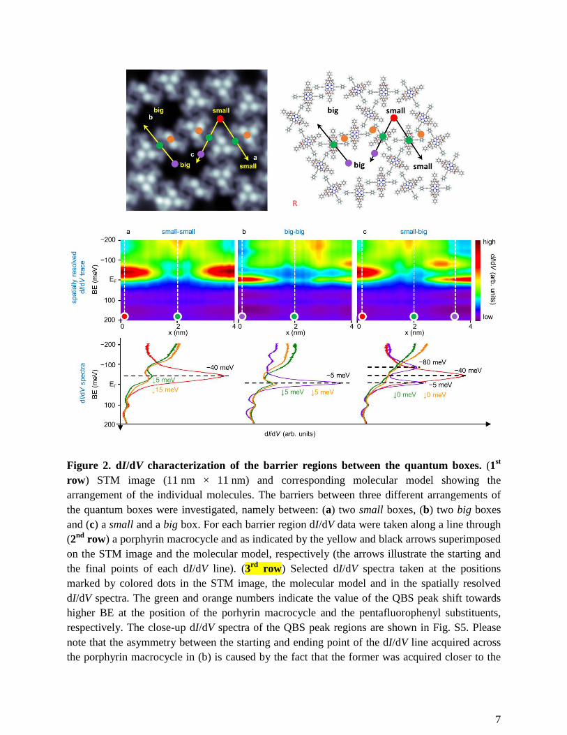
Figure 2. dI/dV characterization of the barrier regions between the quantum boxes. (1st row) STM image (11 nm × 11 nm) and corresponding molecular model showing the arrangement of the individual molecules. The barriers between three different arrangements of the quantum boxes were investigated, namely between: (a) two small boxes, (b) two big boxes and (c) a small and a big box. For each barrier region dI/dV data were taken along a line through (2nd row) a porphyrin macrocycle and as indicated by the yellow and black arrows superimposed on the STM image and the molecular model, respectively (the arrows illustrate the starting and the final points of each dI/dV line). (3rd row) Selected dI/dV spectra taken at the positions marked by colored dots in the STM image, the molecular model and in the spatially resolved dI/dV spectra. The green and orange numbers indicate the value of the QBS peak shift towards higher BE at the position of the porhyrin macrocycle and the pentafluorophenyl substituents, respectively. The close-up dI/dV spectra of the QBS peak regions are shown in Fig. S5. Please note that the asymmetry between the starting and ending point of the dI/dV line acquired across the porphyrin macrocycle in (b) is caused by the fact that the former was acquired closer to the

8
pore centre, which is dominated by the state at −5 meV, whereas the latter closer to the rim of the pore dominated by the state at −80 meV (cf. Fig. S4). For the dI/dV data taken along a line through pentafluorophenyl substituents see Fig. S6.
Quantum confinement in the pores of the network. On Ag(111) the Shockley surface state
disperses across the Fermi level with its energy maximum just below the Fermi level, i.e. at the
binding energy (BE) of 65 meV.45 In the presence of the porous network, the surface state is
shifted above the Fermi level, due to the confinement of the surface state electrons by the pores
of the network, as evidenced by the characteristic peaks in our dI/dV spectra (Fig. 2). Thus, each
pore constitutes a quantum box (QB) embedded in a quantum array. The small pore features a
quantum box state (QBS) peak at BE of −40 meV (Fig. 2a, red spectrum), whereas the big pore
exhibits two peaks: one at −5 meV (Fig. 2b, violet spectrum), dominating in the centre of the
pore and the second one at −80 meV (Fig. 2c, violet spectrum), located at the rim of the pore (the
exact spatial distribution of those QBSs is shown in Fig. S4).
Electronic inter-pore coupling. To modify the transmission probability of the molecular
barrier, first the properties of the unmodified barrier have to be understood. For this purpose,
spatially resolved dI/dV measurements were performed across the network backbone (Fig. 2).
Specifically, the barrier regions of three different pore arrangements were investigated, i.e.
between two small pores, between two big pores, and between a small and a big pore. The barrier
between two small pores is characterized by the presence of a QBS peak, which is shifted
towards higher BE by either ~5 meV at the position of the porphyrin macrocycle or by ~15 meV
at the position of the pentafluorophenyl substituents (Fig. 2a, Fig. S5). At the barrier between
two big pores, the shift amounts to ~5 meV at the position of both the porphyrin macrocycle and
the pentafluorophenyl substituents (Fig. 2b, Fig. S5).
9
It is worth mentioning that the QBS shifts in the barriers of electronically coupled quantum
systems towards higher BE are in accordance with the observations reported by Seufert et al.11
for two coupled quantum wells. The authors demonstrated that in such a system the bonding
component Ψn of the quantum state dominates in the barrier region over the antibonding
component Ψn*. Therefore the former mainly contributes to the dI/dV signal measured above the
barrier, causing the overall shift of the quantum state towards higher BE.
Importantly, first-principle density functional theory (DFT) calculations of a Zn(II)
porphyrin 1 molecule adsorbed on Ag(111) reveal that there is a HOMO-LUMO gap centered
around the Fermi level and that the charge distribution of Ag(111), especially in the first atomic
layer, is significantly affected by the adsorption of Zn(II) porphyrin 1 (Fig. S7). Thus, the
features close to the Fermi level detected in the dI/dV spectra taken at the barriers are QBSs-
related. The penetration into the barrier, and hence also the electronic interaction of the
neighbouring pores, is critically dependent on the interaction of the components of the barrier
with the confined surface state. In our example, both the porphyrin macrocycle and the
pentafluorophenyl substituents affect the confined surface state and thus, both influence the
lateral coupling between neighbouring quantum states.
At the barrier connecting a small pore with a big pore, the quantum states of these pores are
both detected with a very low intensity and without a measurable energy shift (Fig. 2c, Fig. S5).
That means that they both penetrate the barrier. This demonstrates the lack of electronic coupling
between these pores due to the energy level misalignment.
The partial confinement of the Shockley surface state in the pores of the Zn(II) porphyrin 1
network on the Ag(111) surface is also suggested in ARPES data. In Figure 3a ARPES data
collected for a sample partially covered with the network domains is shown. The electronic

10
structure of this system is characterized by two states: (1) the Ag(111) Shockley state (Fig. 3d),
originating from the bare surface, which crosses the Fermi level and reaches its maximum
dispersion at BE ~ 65 meV, and (2) a state dispersing above the Fermi level, originating from the
network, which we attribute to the partially confined state, resulting from the coupling between
the electronic states of the QBs embedded in the array8 (for better visualization, the ARPES
spectrum was integrated over a small k-range around the band centre Fig. 3b, and the energy
distribution curves – EDCs - have been extracted Fig. 3c). Since the band maximum of the QBS
is well above the Fermi level, it is only occupied by the small tail of the thermally broadened
Fermi-Dirac distribution reaching above the Fermi level (note that the ARPES data have been
collected at room temperature). This makes the photoemission intensity of the QBS in this
system very much weaker than that of the Ag(111) Shockley state. One would expect the
(14 × 14)R ± 10° overlayer super-structure to give rise to a reduced Brillouin Zone with
boundaries at k = ±0.08 Å−1, but since the QBS energy at that k value amounts to ~ 200 meV
above the Fermi level, the thermal occupancy of the band results in such a low photoemission
intensity that the presence or absence of this periodicity cannot be confirmed in the presented
ARPES data.

11
Figure 3. Synchrotron-based ARPES measurements of a 2D periodic array of quantum units formed by a Zn(II) porphyrin 1 porous network on Ag(111). (a) ARPES spectrum for a Ag(111) surface partially covered with the Zn(II) porphyrin 1 network: two electronic states are revealed, the Ag(111) Shockley surface state dispersing across the Fermi level and the quantum box state dispersing above the Fermi level. The bottom of both states is fitted by two parabolic dispersions (black lines) and an effective mass is extracted (the fitted points with error bars are marked in red). The parabolas marked by dotted lines indicate the expected periodicity of the QBS. (b) Intensity profile for the spectra in (a) (red curve) obtained by integrating the spectra over the momentum ranges illustrated by the red area in (a). The black line and arrows serve as guides for the eyes. (c) The energy distribution curves (EDCs) at various k values of the data presented in (a). (d) The reference ARPES data for clean Ag(111) surface. The ARPES measurements were carried out at room temperature and at a photon energy of 21 eV. The data were normalized with a Fermi function with a constant offset added to increase the visibility of the state above the Fermi level (see the Materials and methods section for details about the ARPES data analysis including fitting of EDCs and extracting effective mass). STM data acquired at room temperature for an analogue sample is presented in Fig. S8.
Another feature of the network, which also has to be taken into account, is that the vast
majority of the pores is small, as the big pores are observed only at the domain boundaries (cf.
Fig. S2), meaning that mainly the QBS of the former will contribute to the spatially-averaged
ARPES signal. The QBS, however, is detected slightly further away from the Fermi level as by
STS (cf. Fig. 2a and Fig. 3). This difference presumably arises from the temperature dependence
of the energy of the QBS: the higher the temperature the more the confined state shifts towards
lower BE46, the Shockley surface state47 shifts likewise (note that the STS data were acquired at
4.2 K, whereas the ARPES data at room temperature). Additionally an uncertainty in Fermi level
determination of ±10 meV needs to be taken into account.
In order to extract the effective mass (m*) of the system, we have fitted the bottom of both
ARPES spectra of Fig. 3a with parabolas (for details see the Materials and methods section), and
extracted m* = 0.40 ± 0.08 me for the Ag(111) Shockley surface state in agreement with
literature45, and m* = 0.38 ± 0.11 me for the QBS. Thus, we have no evidence for a significant

12
change of the effective mass of the surface state upon the network formation. This is in
agreement with Ref.48, in which the effective mass of the surface state upon metal-organic
network formation on Cu(111) changed from m* = 0.43 ± 0.01 me to m* = 0.57 ± 0.02 me (state
below the Fermi level). In our study, due to the intrinsically reduced intensity above the Fermi
level, the uncertainty in determining m* is significantly higher (± 0.11 me), therefore we cannot
exclude a small change in m* for our QBS, i.e. comparable to the one reported in Ref. 47.
Modification of the inter-pore coupling by adsorbates Next we investigated the possibility of
a modification of the barriers via their interaction with adsorbates. For that purpose we chose two
adsorbates exhibiting characteristically different electronic properties: a closed-shell noble gas
Xe and a strong electron acceptor, fullerene C60.
STM images acquired after Xe exposure revealed that two Xe atoms can adsorb on top of one
porphyrin macrocycle (Fig. 4a). Besides, single Xe atoms adsorb: i) on the porphyrin
macrocycle, ii) between three pentafluorophenyl substituents and iii) between metoxy,
pentafluorophenyl and phenyl groups (Fig. S9). Significantly increased Xe exposure resulted in
the decoration of the network backbone and adsorption at the rim of the pores. No Xe was found
to be adsorbed at the centre of the pores (Fig. S10) pointing at the repulsive interaction between
Xe and the QBS (having its maximum at the centre of the pore), similar to the case of Xe
adsorbed in the pores of the Cu-coordinated 3deh-DPDI network on Cu(111).49 As revealed by
dI/dV measurements (Fig. 4a), the two Xe atoms adsorbed on the porphyrin macrocycle have
almost no influence on the transmission probability of the barrier (red and green dI/dV spectra in
Fig. 4a vs red and green dI/dV spectra in Fig. 2a).

13
Figure 4. Modification of barrier regions between the quantum boxes by adsorbates – STM/STS studies. (a) A barrier with two Xe atoms; (b) a barrier with a single C60 molecule; (c) a barrier with two C60 molecules. (1st row) Molecular models. (2nd row) Corresponding STM images (10 nm x 8 nm). (3rd row) Spatially resolved dI/dV traces acquired along the yellow lines superimposed on the STM images. (4th row) Selected dI/dV spectra taken at the positions indicated by the colored dots in the STM images and in the dI/dV traces. The molecular models overlaid on the STM pictures are presented in Fig. S9b and Fig. S11, whereas the simulated STM images for the case (a) and (b) in Fig. S12.

14
In contrast, a single C60 molecule adsorbed in the pore between two Zn(II) porphyrin
molecules 1 (Fig. 4b) reduces the barrier transmission probability (blue dI/dV spectrum in Fig.4b,
spatially resolved dI/dV traces in Fig. 4b vs in Fig. 2a 2nd row). An even larger reduction of the
transmission probability is caused by two C60 molecules adsorbed in the pore close to the phenyl
groups of three Zn(II) porphyrin molecules 1 (orange dI/dV spectrum in Fig. 4c vs blue dI/dV
spectrum in Fig. 4b).
The presence of C60 molecule(s) in a pore additionally shifts the QBS to lower BE: to ~ –
55 meV in case of a single C60 and to ~ –65 meV in case of two C60 molecules. Importantly, the
reduction of the coupling between the pores is not caused by energy level misalignment, as there
is still an overlap between the quantum states of an empty pore and a pore filled with one C60 or
two C60 molecules. Furthermore C60 molecules do not locally destroy the QBS on the rim of the
pore and thus the inter-pore coupling, as evidenced by the presence of the modified QBS in the
blue dI/dV spectrum in Fig. 4b and the magenta dI/dV spectrum in Fig. S13. Thus, our results
demonstrate that the adsorption of C60 causes both: the modification of the barrier transmission
probability and changes in the quantum box state.
Interestingly, the QBS peak is detected at the same energy at the position of the Zn(II)
porphyrin 1 macrocycle for all three adsorbate cases (cf. gray dashed line in and green dI/dV
spectra in Fig. 4), as for the reference case (cf. dI/dV spectra Fig. 2a). This issue will be
discussed in the following section.
Modification of the confining barrier by adsorbates – DFT insights. In order to understand
the effect of the adsorbates on the confining barriers, we have analyzed the interactions between
the Zn(II) porphyrin 1 adsorbed on Ag(111) and Xe/C60 using DFT. While the reproduction of

15
the entire pore structure is computationally prohibitive, this approach captures the essence of
physics governing the interactions between the confining barriers and the adsorbates.
Our calculations have shown that two Xe atoms can bind on top of the N atoms of the Zn(II)
porphyrin 1 macrocycle, as observed experimentally (cf. Fig. 4a). In this case, the calculated
adsorption energy amounts to only −0.18 eV and no chemical bond is formed (cf. Fig. S14a,c),
suggesting the presence of weak van der Waals interactions. Notably, the two Xe atoms induce
an almost negligible and very localized charge redistribution in Zn(II) porphyrin 1 (less than 0.01
e per Xe atom), while the Ag(111) substrate stays unaffected (Fig. 5a, Fig. S15a). Thus the
confining barrier remains almost unchanged, which explains why its transmission probability is
not detectably modified.

16
Figure 5. Modification of the electronic properties of the confining barrier by adsorbates – DFT calculations. (a) A barrier with two Xe atoms; (b) a barrier with a single C60. (1st row) Optimized structures. (2nd row) and (3rd row) 2D charge difference cuts taken along plane 1 (red) and 2 (blue), respectively, as marked in the optimized structures. The values are given in [e Å−3]. The charge difference was calculated in the following way: Δρq = ρq[adsorbate + Zn(II) porphyrin 1 + Ag(111)] – ρq[Zn(II) porphyrin 1 + Ag(111)] – ρq[adsorbate] (where adsorbate stands either for two Xe atoms or for one C60). In this way, the charge redistribution induced by

17
porphyrin adsorption on Ag(111) is included and the visible changes are only representing the influence of adsorbates.
In agreement with the experiment (cf. Fig. 4b), single C60 favors the adsorption on Ag(111)
close to the Zn(II) porphyrin 1 substituents, while no chemical bond is directly formed between
C60 and Zn(II) porphyrin 1 (Fig. S14b,d). The presence of C60 induces a significant charge
redistribution in the Zn(II) porphyrin 1 substituents and in the pyrrole unit closest to C60, whereas
the centre of the molecule remains almost unaffected (Fig. 5, Fig. 6c, Fig. S13b-16, Movie S1).
Reversely, the presence of the Zn(II) porphyrin 1, results in an energy gain of 0.65 eV for C60,
when compared to the case of isolated C60 on Ag(111). Furthermore, in this configuration the
charge redistribution under the C60 and under the substituents and the pyrrole is distributed
across a larger area of the Ag(111) substrate compared to the case of one isolated C60 adsorbed
on Ag(111) and also compared to the case of one isolated Zn(II) porphyrin 1 on Ag(111) (cf. Fig.
S16, Movie S1). Significant modifications of the confining barrier, in contrast to the case of the
Xe adsorption, are in line with the changes of transmission probability observed experimentally
in the case of C60 adsorption.
Figure 6 | Electronic landscape modification upon deposition of C60 (a) STM image of a pore with a single C60 molecule adsorbed and (b) the corresponding work function map (size: 6 nm x 6 nm). The pyrrole unit and the substituents closest to the adsorbed C60 are more electropositive (green arrow) than the corresponding groups of a Zn(II) porphyrin 1 surrounding an empty pore (yellow arrows). The reference work function map setting the Φ = 0 on Ag(111) is

18
presented in Fig. S17. (c) Top view of 3D charge difference plot; the red isosurface denotes a positive charge density, whereas the blue isosurface denotes a negative charge density (isosurface value ±1.0x10⁻⁴ e Å−3).
Notably, the DFT results are in agreement with the experimentally obtained work function map
displayed in Fig. 6b. It shows that the adsorption of a single C60 near the Zn(II) porphyrin 1
results in the pyrrole unit and the substituents close to the adsorbed C60 being more
electropositive (green arrow) than the corresponding groups of a Zn(II) porphyrin 1 surrounding
an empty pore (yellow arrows). Furthermore, the fact that the macrocycle center of Zn(II)
porphyrin 1, as well as the Ag(111) underneath it, is scarcely affected by the adsorption of either
two Xe atoms or by the adsorption of a single C60 (Fig. 5), agrees well with the observation of
the QBS peak at the same energy (Fig. 4ab, green spectra) as in the reference case (Fig. 2a, green
spectra). On the basis of Fig. S16c, which displays the charge difference plots for single C60
adsorbed near a phenyl of one Zn(II) porphyrin 1, we assume that this is also the case for the
adsorption of two C60 near phenyl groups of three Zn(II) porphyrin 1 molecules (cf. Fig. 4c).
CONCLUSION
In summary, we created an on-surface 2D array of coupled quantum boxes by careful design of
the molecular building block. Upon adsorption of Zn(II) porphyrin 1 on Ag(111), an extended
porous molecular network is formed. The pores confine the Ag(111) surface state and, in
particular, the surface state-derived quantum box state is shifted above the Fermi level. The
quantum boxes are electronically coupled and, importantly, adsorbates, i.e. Xe and C60, show a
distinct influence on the transmission probability of the barrier: while Xe does not detectably
affect it, C60 reduces it significantly. This is confirmed by state-of-the-art DFT calculations,

19
which revealed that Xe has almost no influence on the electronic structure of the confining
barrier, whereas C60 induces a strong charge redistribution within the barrier.
Our results suggest that a wide range of quantum arrays formed from functional molecular
building blocks can be fabricated, and, in combination with different adsorbates, provide a rich
playground for the modification of the quantum box properties. Thus, the quantum states
embedded in on-surface structures can be engineered for exploring physical phenomena, which
could be implemented into future quantum devices.
MATERIALS AND METHODS
Synthesis of Zn(II) porphyrin 1. The synthesis of Zn(II) porphyrin 1 is described in detail in
the Supporting Synthesis file.
Sample preparation for STM/STS measurements The Ag(111) substrate was prepared by
cycles of Ar+ sputtering at E = 1000 eV followed by annealing at 800 K. The Zn(II) porphyrin
molecules 1 were deposited with the use of a 9-cell evaporator (Kentax GmbH, Germany) on the
Ag(111) substrate held at room temperature (RT). The glass crucible with the Zn(II) porphyrin 1
inside was heated up to the sublimation temperature (~320 °C). The rate was controlled prior to
sublimation with a quartz crystal microbalance (QCMB). In order to obtain a porous network, the
molecular rate was lower than 0.4 Å/min. Otherwise, the formation of a close-packed assembly
took place. The C60 molecules (sublimation temperature ~350 °C) were deposited onto the
sample with the porous network held at RT. Xe of purity 99.99% was dosed onto the sample
placed in the STM operating at 4.2 K (Omicron Nanotechnology GmbH with Nanonis SPM
control system) with the cryoshields open and the leak valve being in line-of-sight with the
sample. The STM/STS measurements were performed after cooling the sample back to 4.2 K. In
20
the main text and Figures S1,S2,S4,S6, S9, S11, S13, S17 the STM/STS data for a sample after
10 Langmuir (1.3 × 10⁻⁷ mbar for 100 s) of Xe exposure are shown. Figure S10 presents the
STM data taken after 100 Langmuir of Xe exposure, in which case the dosing time was increased
10 times by maintaining the same pressure as in the previous case. Both exposures resulted in an
increase of the sample temperature to 8 K due to opening the cryoshield.
Note that all STM/STS data were acquired at 4.2 K, apart from Fig. S8 in which case the STM
was operated at room temperature.
STM/STS measurements and their analysis For the STM measurements, the bias voltage is
applied to the tip. The bias voltages in the manuscript and the Supporting Data File refer to a
grounded tip, such that the voltage axis in the dI/dV data can be related to the binding energy
(BE) of the ARPES data.
STM measurements were performed in constant current mode with Pt-Ir tips (90% Pt, 10% Ir),
prepared by mechanical cutting followed by sputtering and controlled indentation in the bare
Ag(111) substrate. The majority STM images was acquired with a single Xe atom functionalized
tip (cf. Tab. S1), which increases the spatial resolution. The exact tunneling parameters for the
STM images presented in the main text and Supporting Data File are displayed in Tab. S1. The
STM data were processed with the WSxM software.50 For better comparability of the data, the
color histograms of the STM images were adjusted. Low-pass filtering was used for noise
reduction.
All dI/dV spectra were recorded with open-feedback loop and with Xe-functionalized tips.
Control spectra were acquired with a metallic tip, and no difference was observed in accordance
with Ref.51. The lock-in parameters were 513 Hz (frequency) and 8 mV (zero-to-peak
amplitude).

21
The dI/dV data presented in Fig. 2, Fig. 4, Fig. S4, Fig. S6 were acquired along the line
indicated in the corresponding STM images and are displayed in form of spatially resolved dI/dV
traces. The amount of measurement points for the traces was adjusted in dependence on the
measured barrier (from 40 to 80 points per line). The initial tip conditions when taking dI/dV
spectra amounted to -200 mV/150 pA, with the exception of the dI/dV data shown Fig. 4a, in
which case -200 mV/50 pA was used. The reason for more delicate initial tip conditions when
investigating Xe atoms adsorbed on a Zn(II) porphyrin 1 macrocycle is the relatively weak
interaction strength, which led to desorption when harsher dI/dV parameters were applied. The
dI/dV maps presented in Fig. S4 were extracted from a grid spectroscopy measurement, in which
an area of 6 nm × 5 nm was mapped with a resolution of 30 points × 25 points. At each point, a
dI/dV spectrum was measured (initial tip conditions -200 mV/150 pA). As described in detail in
Ref. 52, the value of the initial voltage was chosen such, that no quantum box state or network
backbone-related contribution was present (cf. Fig. S7a). Owing to this, a normalization
procedure could be performed by setting the same dI/dV value at the setpoint energy for all dI/dV
spectra. In this way, artefacts originating from local work function variations are eliminated.
I(z) measurements and their analysis. The work function maps presented in Fig. 6 and
Fig. S17 were obtained with the use of methods developed by Vitali et al.53 The maps were
extracted from a grid spectroscopy measurement, in which at each point I(z) curves were
measured. From an exponential fit of the average of three I(z) curves, the work function was
extracted for each point.
LEED measurements and their analysis. The LEED measurements were performed with the
use of a V. G. Electrovac LTD 474 unit. The LEED data were taken at energies between 5 eV
and 60 eV. For simulating the experimentally obtained patterns the software LEEDpat 2.1

22
(K. Hermann, M. A. van Hove, LEED pattern simulator LEEDpat Version 2.1, 2006) was used
(cf. Fig. 1c, Fig. S3).
ARPES measurements and their analysis. ARPES data were acquired at the beamline I3 of
the synchrotron radiation source of MAX-III (Lund, Sweden). The Ag(111) crystal was prepared
by consecutive cycles of Ar+ sputtering and annealing, similarly to the preparation used for the
STM/STS measurements. The Zn(II) porphyrin molecules 1 were deposited with the use of a
home-made evaporator. The rate prior to deposition was checked by QCMB.
It is worth mentioning that collecting ARPES data from organic materials is a challenging
task8, as organic molecules can be destroyed by the incident UV light (beam-damage). A way to
overcome this problem is to use a defocused light source and low photon energies for the
experiment. Therefore beamline undulator was detuned in order to reduce the intensity of the
photon beam, hence avoiding any radiation damage to the sample. The slits were set such that a
light spot of 0.5 mm on the sample was obtained. Such a large light spot minimizes flux (and
hence beam-damage), but causes a reduction in the angular resolution (and hence momentum
resolution) of the ARPES measurement, estimated to be 0.04 1/Å for the measurements
presented in Fig. 3 of the main text. A photon energy of 21 eV was sufficient to keep the
molecules intact over the whole acquisition time amounting to ~1 h. Moreover, no signs of
degradation in the ARPES data were observed, even after several hours of experimental time,
demonstrating the full viability of this approach for studying the particular system presented
here.
The ARPES measurements were carried out at normal emission and at room temperature. The
choice of the temperature is extremely important, since it induces a broadening of the Fermi-
Dirac distribution, resulting in a promotion of thermal electrons from states below to states above

23
the Fermi level. This allows the detection of electronic states even at energies above the Fermi
level. However, the spectral intensity of such states is so weak that it is barely detectable by eye.
In order to enhance the intensity of these states with respect to the intensities below the Fermi
level, we normalized the data by a Fermi function at room temperature. In addition, since the
Fermi function goes exponentially to zero for low BE values, in order to avoid numerical issues
in dividing the spectral intensity by 'zero', we added a small constant to the Fermi function (i.e.
0.03). Whilst the normalization allows an exceptionally good enhancement of the spectral
features above the Fermi level, it artificially moves the centre of mass of the spectral intensity
towards the Fermi level, resulting in an apparent small energy shift of the band minimum. Fig.
S18 displays the raw data, the raw data with amplified intensity and the normalized data. In Fig.
S19 raw and normalized ARPES data of bare Ag(111) is shown. In the such treated data, there is
no additional state, which demonstrates the validity of the used normalization procedure.
From the ARPES data presented in Fig. 3a, EDCs have been extracted at different values of
momentum k, and each individual EDC has been fitted by a Lorentzian component convoluted
with a Gaussian component, to account for the energy resolution of the instrument. From the fits,
the peak positions are readily extracted, together with their corresponding uncertainties (red
points and error bars in Fig. 3a). Those peak positions have been fitted with parabolas (Fig. 3a),
from the curvature of which the effective masses were extracted.
DFT calculations. First-principle density functional theory calculations were performed using
the Vienna ab initio simulation code (VASP)54–57 with the generalized gradient approximation
(GGA) and the projector augmented wave (PAW) method.58,59 The plane-wave cutoff energy
was set to 400 eV. The adsorption of Zn(II) porphyrin 1, C60, Xe and their co-adsorption on the
three layer FCC slabs of Ag (111) was modelled using 10×10 supercell. The vacuum layer

24
thickness was about 17 Å. Atoms of the bottom layer of the Ag slab were kept fixed. All the
other atoms were fully relaxed until the residual forces became less than 0.02 eV/Å. The
structural optimization was performed using the Γ k-point. Gaussian smearing was applied to
improve convergence. Additional calculations using larger supercell (the systems containing up
to 800 atoms) showed that the adsorption energies of Zn(II) porphyrin 1 and C60, as well as the
charge redistribution, are almost unaffected by the size of the simulation cell. Our preliminary
calculations showed that the dispersion interactions play very important role when considering
the adsorption of Zn(II) porphyrin 1 on Ag(111). For this reason we included dispersion
interactions using the semi-empirical model by Grimme (PBE+D2)60,61 for all the systems
analyzed here. Compared to GGA-PBE, which gave Ag lattice constant of 4.145 Å, PBE+D2
approach gave 4.121 Å, which better agrees with the experimental value (4.079 Å). The charge
analysis was carried out using the Bader algorithm62 on a charge density grid by Henkelman et
al.63
ASSOCIATED CONTENT
Supporting Information.
Supporting Information contains additional experimental and theoretical data and detailed
information about the synthesis of Zn(II) porphyrin 1; The Supporting Information is available
free of charge on the ACS Publications website at DOI:
Supporting Data file: the file contains additional STM and ARPES data, results of DFT
calculations in terms of DOS of Zn(II) porphyrin 1 molecule, charge density difference plots,
electron localization function maps, experimentally derived work function maps, ARPES data of
bare Ag(111) and tabulated tunneling parameters of STM images presented in the main text and

25
the Supporting Data file. All Supporting Figures referred to in the main text are assembled in this
file (Fig. S1-S19, Tab. S1) (PDF)
Supporting Synthesis file: the file containing detailed description of synthesis and
characterization (XRD single crystal, spectroscopic data) of Zn(II) porphyrin 1 (PDF)
Supporting Movie S1: volume slice through the charge difference volumetric data of C60
adsorbed at two different positions with respect to Zn(II) porphyrin 1 on Ag(111) (GIF)
CCDC-1455039 (1) contain the supporting crystallographic data for this paper. These data can
be obtained free of charge from the Cambridge Crystallographic Data Centre, 12 Union Road,
Cambridge CB21EZ, UK (fax: +44 1223 336 033; e-mail: [email protected]), or via
www.ccdc.cam.ac.uk/data_request/cif
Financial interest statements.
The authors declare no competing financial interest.
AUTHOR INFORMATION
Author Contributions
The manuscript was written through contributions of all authors. All authors have given approval
to the final version of the manuscript.
ACKNOWLEDGMENT
In memoriam Max Broszio
Authors would like to acknowledge the financial support from the Swiss National Science
Foundation (grants No. 200020-149713, 206021-121461, 206021-113149, 206021-144991,
200020-153549) and the National Centre of Competence in Research “Nanoscience” (NCCR-

26
Nano, project “Nanoscale Science”), Swiss Nanoscience Institute (SNI) (Project No. P1204 and
P1203), Marie-Curie Research Training Network PRAIRIES (grant No. MRTN-CT-2006-
035810), Norwegian University of Science and Technology, MAX-lab, Swedish Research Links
initiative of the Swedish Research Council (348-2012-6196), and the Swedish Research Council
project no. 2014-5993, the São Paulo Research Foundation (grant No. 2013/04855-0), Swiss
Government Excellence Scholarship Program (grant No. 2013.0942), Netherlands Organization
for Scientific Research NWO (Chemical Sciences, VIDI-grant No. 700.10.424) the European
Research Council (ERC-2012-StG 307760-SURFPRO), the Hundred Talents project of the
Chinese Academy of Sciences, Knut and Alice Wallenberg Foundation, Commission for
Technology and Innovation (CTI) Contract No. 16464.1 PFNM-NM, University of Basel, ETH
Zürich, University Research Priority Program LightChEC of the University of Zürich, University
of Groningen, Swiss Light Source, Wolfermann Naegeli Foundation and Paul Scherrer Institute.
The research of M.N.A. is implemented within the framework of the Action «Supporting
Postdoctoral Researchers» of the Operational Program "Education and Lifelong Learning"
(Action’s Beneficiary: General Secretariat for Research and Technology) co-financed by the
European Social Fund (ESF) and the Greek State. The computations were performed on
resources provided by the Swedish National Infrastructure for Computing (SNIC) at National
Supercomputer Centre (NSC) at Linköping University. We sincerely thank M. Martina for
technical support.
REFERENCES
(1) Kagan, C. R.; Murray, C. B. Charge Transport in Strongly Coupled Quantum Dot Solids. Nat. Nanotechnol. 2015, 10, 1013–1026.
(2) Shirasaki, Y.; Supran, G. J.; Bawendi, M. G.; Bulović, V. Emergence of Colloidal Quantum-Dot Light-Emitting Technologies. Nat. Photonics 2012, 7, 13–23.

27
(3) Stranks, S. D.; Snaith, H. J. Metal-Halide Perovskites for Photovoltaic and Light-Emitting Devices. Nat. Nanotechnol. 2015, 10, 391–402.
(4) Ladd, T. D.; Jelezko, F.; Laflamme, R.; Nakamura, Y.; Monroe, C.; O’Brien, J. L. Quantum Computers. Nature 2010, 464, 45–53.
(5) Gross, L.; Moresco, F.; Savio, L.; Gourdon, A.; Joachim, C.; Rieder, K.-H. Scattering of Surface State Electrons at Large Organic Molecules. Phys. Rev. Lett. 2004, 93.
(6) Silly, F.; Pivetta, M.; Ternes, M.; Patthey, F.; Pelz, J. P.; Schneider, W.-D. Creation of an Atomic Superlattice by Immersing Metallic Adatoms in a Two-Dimensional Electron Sea. Phys. Rev. Lett. 2004, 92, 016101.
(7) Han, P.; Weiss, P. S. Electronic Substrate-Mediated Interactions. Surf. Sci. Rep. 2012, 67, 19–81.
(8) Lobo-Checa, J.; Matena, M.; Muller, K.; Dil, J. H.; Meier, F.; Gade, L. H.; Jung, T. A.; Stohr, M. Band Formation from Coupled Quantum Dots Formed by a Nanoporous Network on a Copper Surface. Science 2009, 325, 300–303.
(9) Klappenberger, F.; Kühne, D.; Krenner, W.; Silanes, I.; Arnau, A.; García de Abajo, F. J.; Klyatskaya, S.; Ruben, M.; Barth, J. V. Dichotomous Array of Chiral Quantum Corrals by a Self-Assembled Nanoporous Kagomé Network. Nano Lett. 2009, 9, 3509–3514.
(10) Klappenberger, F.; Kühne, D.; Krenner, W.; Silanes, I.; Arnau, A.; García de Abajo, F. J.; Klyatskaya, S.; Ruben, M.; Barth, J. V. Tunable Quantum Dot Arrays Formed from Self-Assembled Metal-Organic Networks. Phys. Rev. Lett. 2011, 106, 026802.
(11) Seufert, K.; Auwärter, W.; Garcı́a de Abajo, F. J.; Ecija, D.; Vijayaraghavan, S.; Joshi, S.; Barth, J. V. Controlled Interaction of Surface Quantum-Well Electronic States. Nano Lett. 2013, 13, 6130–6135.
(12) Li, J.; Schneider, W.-D.; Berndt, R.; Crampin, S. Electron Confinement to Nanoscale Ag Islands on Ag(111): A Quantitative Study. Phys. Rev. Lett. 1998, 80, 3332–3335.
(13) Crommie, M. F.; Lutz, C. P.; Eigler, D. M. Confinement of Electrons to Quantum Corrals on a Metal Surface. Science 1993, 262, 218–220.
(14) Nilius, N.; Wallis, T. M.; Ho, W. Development of One-Dimensional Band Structure in Artificial Gold Chains. Science 2002, 297, 1853–1856.
(15) Pennec, Y.; Auwärter, W.; Schiffrin, A.; Weber-Bargioni, A.; Riemann, A.; Barth, J. V. Supramolecular Gratings for Tuneable Confinement of Electrons on Metal Surfaces. Nat. Nanotechnol. 2007, 2, 99–103.
(16) Shchyrba, A.; Martens, S. C.; Wäckerlin, C.; Matena, M.; Ivas, T.; Wadepohl, H.; Stöhr, M.; Jung, T. A.; Gade, L. H. Covalent Assembly of a Two-Dimensional Molecular “sponge” on a Cu(111) Surface: Confined Electronic Surface States in Open and Closed Pores. Chem. Commun. 2014, 50, 7628–7631.
(17) Zhang, J.; Shchyrba, A.; Nowakowska, S.; Meyer, E.; Jung, T. A.; Muntwiler, M. Probing the Spatial and Momentum Distribution of Confined Surface States in a Metal Coordination Network. Chem. Commun. 2014, 50, 12289–12292.
(18) Schouteden, K.; Ivanova, T.; Li, Z.; Iancu, V.; Tahara, K.; Tobe, Y.; Adisoejoso, J.; Feyter, S. D.; Haesendonck, C. V.; Janssens, E. Alkoxylated dehydrobenzo[12]annulene on Au(111): From Single Molecules to Quantum Dot Molecular Networks. Chem. Commun. 2015, 51, 10917–10920.
(19) Wang, S.; Wang, W.; Tan, L. Z.; Li, X. G.; Shi, Z.; Kuang, G.; Liu, P. N.; Louie, S. G.; Lin, N. Tuning Two-Dimensional Band Structure of Cu(111) Surface-State Electrons That Interplay with Artificial Supramolecular Architectures. Phys. Rev. B 2013, 88, 245430.

28
(20) Cheng, Z.; Wyrick, J.; Luo, M.; Sun, D.; Kim, D.; Zhu, Y.; Lu, W.; Kim, K.; Einstein, T. L.; Bartels, L. Adsorbates in a Box: Titration of Substrate Electronic States. Phys. Rev. Lett. 2010, 105, 066104.
(21) Pivetta, M.; Pacchioni, G. E.; Schlickum, U.; Barth, J. V.; Brune, H. Formation of Fe Cluster Superlattice in a Metal-Organic Quantum-Box Network. Phys. Rev. Lett. 2013, 110, 086102.
(22) Müller, K.; Enache, M.; Stöhr, M. Confinement Properties of 2D Porous Molecular Networks on Metal Surfaces. J. Phys. Condens. Matter 2016, 28, 153003.
(23) Piquero-Zulaica, I.; Lobo-Checa, J.; Sadeghi, A.; El-Fattah, Z. M. A.; Mitsui, C.; Okamoto, T.; Pawlak, R.; Meier, T.; Arnau, A.; Ortega, J. E.; et al. Precise Engineering of Quantum Dot Array Coupling through Their Barrier Widths. Nat. Commun. 2017, 8.
(24) Mazzola, F.; Polley, C. M.; Miwa, J. A.; Simmons, M. Y.; Wells, J. W. Disentangling Phonon and Impurity Interactions in δ-Doped Si(001). Appl. Phys. Lett. 2014, 104, 173108.
(25) Ortega, J. E.; Lobo-Checa, J.; Peschel, G.; Schirone, S.; Abd El-Fattah, Z. M.; Matena, M.; Schiller, F.; Borghetti, P.; Gambardella, P.; Mugarza, A. Scattering of Surface Electrons by Isolated Steps versus Periodic Step Arrays. Phys. Rev. B 2013, 87, 115425.
(26) Mazzola, F.; Wells, J. W.; Yakimova, R.; Ulstrup, S.; Miwa, J. A.; Balog, R.; Bianchi, M.; Leandersson, M.; Adell, J.; Hofmann, P.; et al. Kinks in the σ Band of Graphene Induced by Electron-Phonon Coupling. Phys. Rev. Lett. 2013, 111.
(27) Howard, J. A. K.; Hoy, V. J.; O’Hagan, D.; Smith, G. T. How Good Is Fluorine as a Hydrogen Bond Acceptor? Tetrahedron 1996, 52, 12613–12622.
(28) Schneider, H.-J. Hydrogen Bonds with Fluorine. Studies in Solution, in Gas Phase and by Computations, Conflicting Conclusions from Crystallographic Analyses. Chem. Sci. 2012, 3, 1381.
(29) Dunitz, J. D.; Taylor, R. Organic Fluorine Hardly Ever Accepts Hydrogen Bonds. Chem. - Eur. J. 1997, 3, 89–98.
(30) Meanwell, N. A.; Eastman, K. J.; Gillis, E. P. Tactical Applications of Fluorine in Drug Design and Development. In Fluorine in Heterocyclic Chemistry Volume 1; Nenajdenko, V., Ed.; Springer International Publishing: Cham, 2014; Vol. Chapter 6.1, pp. 1–54.
(31) Shimoni, L.; Glusker, J. P. The Geometry of Intermolecular Interactions in Some Crystalline Fluorine-Containing Organic Compounds. In Science of Crystal Structures; Hargittai, I.; Hargittai, B., Eds.; Springer International Publishing: Cham, 2015; pp. 187–203.
(32) Hipps, K. W.; Scudiero, L.; Barlow, D. E.; Cooke, M. P. A Self-Organized 2-Dimensional Bifunctional Structure Formed by Supramolecular Design. J Am Chem Soc 2002, 124, 2126–2127.
(33) Mu, Z.; Shu, L.; Fuchs, H.; Mayor, M.; Chi, L. Two Dimensional Chiral Networks Emerging from the Aryl−F···H Hydrogen-Bond-Driven Self-Assembly of Partially Fluorinated Rigid Molecular Structures. J Am Chem Soc 2008, 130, 10840–10841.
(34) Calzolari, A.; Jin, W.; Reutt-Robey, J. E.; Buongiorno Nardelli, M. Substrate-Mediated Intermolecular Hybridization in Binary Phthalocyanine Superstructures. J. Phys. Chem. C 2010, 114, 1041–1045.
(35) Wäckerlin, C.; Nowakowski, J.; Liu, S.-X.; Jaggi, M.; Siewert, D.; Girovsky, J.; Shchyrba, A.; Hählen, T.; Kleibert, A.; Oppeneer, P. M.; et al. Two-Dimensional Supramolecular Electron Spin Arrays. Adv. Mater. 2013, 25, 2404–2408.

29
(36) Kawai, S.; Sadeghi, A.; Feng, X.; Lifen, P.; Pawlak, R.; Glatzel, T.; Willand, A.; Orita, A.; Otera, J.; Goedecker, S.; et al. Obtaining Detailed Structural Information about Supramolecular Systems on Surfaces by Combining High-Resolution Force Microscopy with Ab Initio Calculations. ACS Nano 2013, 7, 9098–9105.
(37) Wintjes, N.; Bonifazi, D.; Cheng, F.; Kiebele, A.; Stöhr, M.; Jung, T.; Spillmann, H.; Diederich, F. A Supramolecular Multiposition Rotary Device. Angew. Chem. Int. Ed. 2007, 46, 4089–4092.
(38) Wintjes, N.; Hornung, J.; Lobo‐Checa, J.; Voigt, T.; Samuely, T.; Thilgen, C.; Stöhr, M.; Diederich, F.; Jung, T. A. Supramolecular Synthons on Surfaces: Controlling Dimensionality and Periodicity of Tetraarylporphyrin Assemblies by the Interplay of Cyano and Alkoxy Substituents. Chem. - Eur. J. 2008, 14, 5794–5802.
(39) Écija, D.; Seufert, K.; Heim, D.; Auwärter, W.; Aurisicchio, C.; Fabbro, C.; Bonifazi, D.; Barth, J. V. Hierarchic Self-Assembly of Nanoporous Chiral Networks with Conformationally Flexible Porphyrins. ACS Nano 2010, 4, 4936–4942.
(40) Pace, C. J.; Gao, J. Exploring and Exploiting Polar−π Interactions with Fluorinated Aromatic Amino Acids. Acc. Chem. Res. 2013, 46, 907–915.
(41) Reichenbächer, K.; Süss, H. I.; Hulliger, J. Fluorine in Crystal Engineering—“the Little Atom That Could.” Chem Soc Rev 2005, 34, 22–30.
(42) Schwarzer, A.; Weber, E. Penta- and Decafluorinated Dibenzalacetones: Synthesis, Crystal Structure, and Cocrystallization Experiments. Cryst. Growth Des. 2014, 14, 2335–2342.
(43) Ponzini, F.; Zagha, R.; Hardcastle, K.; Siegel, J. S. Phenyl/Pentafluorophenyl Interactions and the Generation of Ordered Mixed Crystals:sym-Triphenethynylbenzene Andsym-Tris(perfluorophenethynyl)benzene. Angew. Chem. Int. Ed. 2000, 39, 2323–2325.
(44) Coates, G. W.; Dunn, A. R.; Henling, L. M.; Dougherty, D. A.; Grubbs, R. H. Phenyl–Perfluorophenyl Stacking Interactions: A New Strategy for Supermolecule Construction. Angew. Chem. Int. Ed. Engl. 1997, 36, 248–251.
(45) Reinert, F.; Nicolay, G.; Schmidt, S.; Ehm, D.; Hüfner, S. Direct Measurements of the L-Gap Surface States on the (111) Face of Noble Metals by Photoelectron Spectroscopy. Phys. Rev. B 2001, 63, 115415.
(46) Piquero-Zulaica, I.; Nowakowska, S.; Ortega, J. E.; Stöhr, M.; Gade, L. H.; Jung, T. A.; Lobo-Checa, J. Temperature Dependence of the Partially Localized State in a 2D Molecular Nanoporous Network. Appl. Surf. Sci. 2016, 391, 39–43.
(47) Paniago, R.; Matzdorf, R.; Meister, G.; Goldmann, A. Temperature Dependence of Shockley-Type Surface Energy Bands on Cu(111), Ag(111) and Au(111). Surf. Sci. 1995, 336, 113–122.
(48) Nowakowska, S.; Wäckerlin, A.; Piquero-Zulaica, I.; Nowakowski, J.; Kawai, S.; Wäckerlin, C.; Matena, M.; Nijs, T.; Fatayer, S.; Popova, O.; et al. Configuring Electronic States in an Atomically Precise Array of Quantum Boxes. Small 2016, 12, 3757–3763.
(49) Nowakowska, S.; Wäckerlin, A.; Kawai, S.; Ivas, T.; Nowakowski, J.; Fatayer, S.; Wäckerlin, C.; Nijs, T.; Meyer, E.; Björk, J.; et al. Interplay of Weak Interactions in the Atom-by-Atom Condensation of Xenon within Quantum Boxes. Nat. Commun. 2015, 6, 6071.
(50) Horcas, I.; Fernández, R.; Gómez-Rodríguez, J. M.; Colchero, J.; Gómez-Herrero, J.; Baro, A. M. WSXM: A Software for Scanning Probe Microscopy and a Tool for Nanotechnology. Rev. Sci. Instrum. 2007, 78, 013705.
30
(51) Manoharan, H. C.; Lutz, C. P.; Eigler, D. M. Quantum Mirages Formed by Coherent Projection of Electronic Structure. Nature 2000, 403, 512–515.
(52) Krenner, W.; Kühne, D.; Klappenberger, F.; Barth, J. V. Assessment of Scanning Tunneling Spectroscopy Modes Inspecting Electron Confinement in Surface-Confined Supramolecular Networks. Sci. Rep. 2013, 3.
(53) Vitali, L.; Levita, G.; Ohmann, R.; Comisso, A.; De Vita, A.; Kern, K. Portrait of the Potential Barrier at Metal-Organic Nanocontacts. Nat. Mater. 2010, 9, 320–323.
(54) Kresse, G.; Hafner, J. Ab Initio Molecular Dynamics for Liquid Metals. Phys. Rev. B 1993, 47, 558–561.
(55) Kresse, G.; Hafner, J. Ab Initio Molecular-Dynamics Simulation of the Liquid-Metal–amorphous-Semiconductor Transition in Germanium. Phys. Rev. B 1994, 49, 14251–14269.
(56) Kresse, G.; Furthmüller, J. Efficiency of Ab-Initio Total Energy Calculations for Metals and Semiconductors Using a Plane-Wave Basis Set. Comput. Mater. Sci. 1996, 6, 15–50.
(57) Kresse, G.; Furthmüller, J. Efficient Iterative Schemes for Ab Initio Total-Energy Calculations Using a Plane-Wave Basis Set. Phys. Rev. B 1996, 54, 11169–11186.
(58) Blöchl, P. E. Projector Augmented-Wave Method. Phys. Rev. B 1994, 50, 17953–17979. (59) Kresse, G.; Joubert, D. From Ultrasoft Pseudopotentials to the Projector Augmented-Wave
Method. Phys. Rev. B 1999, 59, 1758–1775. (60) Grimme, S. Accurate Description of van Der Waals Complexes by Density Functional
Theory Including Empirical Corrections. J. Comput. Chem. 2004, 25, 1463–1473. (61) Grimme, S. Semiempirical GGA-Type Density Functional Constructed with a Long-
Range Dispersion Correction. J. Comput. Chem. 2006, 27, 1787–1799. (62) Bader, R. F. W. Atoms in Molecules: A Quantum Theory; The International series of
monographs on chemistry; Clarendon Press ; Oxford University Press: Oxford [England] : New York, 1994.
(63) Henkelman, G.; Arnaldsson, A.; Jónsson, H. A Fast and Robust Algorithm for Bader Decomposition of Charge Density. Comput. Mater. Sci. 2006, 36, 354–360.

31
For Table of Contents Only