universiti putra malaysia fabrication and …psasir.upm.edu.my/12153/1/fk_2003_12_a.pdf · j.lm...
TRANSCRIPT
UNIVERSITI PUTRA MALAYSIA
FABRICATION AND CHARACTERIZATION OF O.5-um MOSFET BULK SILICON TECHNOLOGY ON THICK BONDED SILICON-ON-INSULATOR SUBSTRATE
WAN FAZLIDA HANIM ABDULLAH
FK 2003 12

FABRICATION AND CHARACTERIZATION OF O.S-J,lm MOSFET BULK SILICON TECHNOLOGY ON THICK BONDED SILICON-ON-INSULATOR
SUBSTRATE
By
WAN FAZLIDA HANIM ABDULLAH
Thesis submitted to the School of Graduate Studies, U niversiti Putra Malaysia in FulfiUment of the Requirement for the
Degree of Master of Science
March 2003

Abstract of thesis presented to the Senate ofUniversiti Putra Malaysia in fulfilment of the requirements for the degree of Master of Science
F ABRICA TION AND CHARACTERIZATION OF 0.5-J,Lm MOSFET BULK SILICON TECHNOLOGY ON THICK BONDED SILICON-ON-INSULATOR
SUBSTRATE
By
WAN F AZLIDA HANIM ABDULLAH
March 2003
Chairman Dr. Roslina Mohd Sidek
Faculty Engineering
The effect of thick film Silicon-On-Insulator (SOl) substrate on device fabrication
and performance is studied. Enhancement-type Partially-Depleted SOl MOS device
is fabricated on bonded SOl (BSOI) substrate based on bulk silicon MIMOS 0.5 J.Lffi
CMOS technology with full compatibility maintained. The substrate employed is
commercially available with the specification 1.5 J.Lffi silicon device layer with ±0.5
J.lm within wafer variation on 2 J.Lffi buried oxide achieved by bonding followed by
mechanical thinning ..
Prior to device fabrication, sacrificial oxidation is applied to adjust the top silicon
layer thickness. Throughout the fabrication, monitoring steps using spectroscopic
reflectometry technique are taken in ensuring enough silicon thickness is left on the
top BSOI surface for device construction. To allow comparison of substrate effects,
bulk silicon substrates are included in the fabrication as control wafers.
11

Three main electrical parameters were extracted from all sites of all the wafers.
Bonded SOl (BSOI) substrate is observed to undesirably increase threshold voltage
and decrease drive current capability. Sacrificial oxidation technique to adjust the
silicon layer thickness worsens device performance and yield. However, BSOI
substrate offers much improved off-state leakage current compared to bulk devices.
Further current-voltage sweep data analysis show that BSOI substrate improves the
subthreshold slope, reduces the drain-induced barrier lowering effect and improves
resistance towards latchup. Peculiar device characteristics typical to Partially
Depleted SOl devices were observed from the output characteristics. These include
early breakdown voltage, negative conductance in the saturation region of body
contacted devices at high gate voltages and kink effect when the body is left floating.
The results show that SOl fabrication is achievable using existing bulk silicon
fabrication technology. Even though devices on BSOI substrate show certain
improvements in device characteristics, the full potential of the SOl structure could
not be achieved with the thickness and uniformity of the BSOI substrate applied.
iii

Abstrak tesis yang dikemukakan kepada Senat Universiti Putra Malaysia sebagai memenuhi keperluan untuk ijazah Master Sains
FABRIKASI DAN PENCIRIAN PERANTI MOSFET O.5-�m TEKNOLOGI SILIKON BONGKAH DI ATAS SUBSTRAT SILIKON-ATAS-PENEBAT
TERIKAT
Oleh
WAN F AZLIDA HANIM ABDULLAH
Mac 2003
Pengerusi Dr. RosUna Mobd Sidek
Fakulti Kejuruteraan
Kajian dilakukan ke atas kesan substrat silikon-atas-penebat (SOl) lapisan silikon
tebal terhadap fabrikasi dan prestasi operasi peranti. Peranti MOS jenis peningkatan
separa-susut difabrikasi atas substrat SOl terikat (BSOI) berdasarkan teknologi
silikon bongkah 0.5-� CMOS hak MIMOS dengan mengekalkan keserasian proses
fabrikasi sepenuhnya. Substrat SOl yang digunakan boleh diperolehi secara komersil
dengan spesifikasi lapisan silikon 1.5 � dengan variasi ± 0.5 J.LIIl di atas oks ida
tertanam setebal 2 � yang disediakan menggunakan teknik pengikatan diikuti
dengan penipisan mekanikaL
Sebelum pemprosesan peranti bermula, pengoksidanan korban dilakukan bagi
menipiskan lagi lapis silikon di atas penebat. Langkah pengawasan diambil
sepanjang pemprosesan peranti bagi memastikan ketebalan yang mencukupi masih
terdapat pada lapisan atas substrat untuk pembuatan peranti. Bagi membolehkan
perbandingan kesan substrat dikaji, substrat silikon keseluruhan disertakan sepanjang
fabrikasi sebagai wafer kawalan.
IV

Tiga parameter elektrikal utama diekstrak dari setiap tapak peranti kesemua wafer.
Substrat (BSOl) memberi kesan yang tidak dingini dengan meninggikan voltan
ambang dan merendahkan daya arus. Teknik penipisan lapisan silikon secara
pengoksidanan korban menerukkan lagi prestasi peranti dan peratusan penghasilan.
Walau bagaimanapun, substrat BSOl menjadikan arus boeor status tutup jelas lebib
baik berbanding peranti silikon keseluruhan.
Analisa lanjutan ke atas data arus-voltan menunjukkan substrat BSOl
memperelokkan keeerunan bawah ambang, ,mengurangkan kesan perendahan
kawasan susutan eetusan parit dan menambahkan kekebalan terhadap fenomena
lekapan. Melalui pendemonstrasian eiri luaran arus-voltan, eiri peranti separa-susut
SOl dapat diperhatikan. Antaranya adalah voltan runtuhan awal, konduksi negatif
dalam kawasan tepu pada voltan get tinggi dan kesan penambahan mendadak pada
arus parit apabila badan peranti dibiarkan terapung.
Hasil penyelidikan menunjukkan bahawa fabrikasi peranti SOl boleh dieapai
menggunakan teknologi silikon bongkah. Walaupun peranti di alas substrat BSOl
mempamirkan eiri peranti tertentu yang semakin baik, potensi struktur SOl tidak
dapat dimanfaatkan sepenuhnya dengan ketebalan dan ketidak-seragaman substrat
BSOl yang diguna-pakai.
v

ACKNOWLEDGEMENTS
All praise be to Allah.
r am grateful to Dr Roslina Sidek for the supervision and making obstacles look less
intimidating. To Dr Mohd Rais Ahmad of MIMOS Berhad, thank you for providing
insight to research approach and support given throughout the research. I am also
thankful to En Rahman Wagiran and En Nasri Sulaiman for having trust in me.
I am indebted to MIMOS Berhad for allowing academic research to be implemented
in the highly sensitive, expensive and confidential environment of the wafer
fabrication facility. A big thank you is all I can give to the helpful and smiling staff
of MIMOS: Rofei and Dr Ismat, for all the answers to all the questions on device
fabication and simulation; Shabrul Arnan, Amri and Suriani, for the training and
technical support on everything under the roof of electrical testing; Ramzan, the
"originator" of the SOL implementation; Azlina, for the help with Nanospec; Zaliha,
for the explanations and recipe preparation on oxidation and wet etch; the FA group
for SEM pictures and all who helped and supported the project.
On a personal note, r must fmd a place to record my gratitude to my husband for all
the IT technical help which I am most hopeless at and the grouches we enjoyed
making but not enjoy paying on toll fares and petrol consumption along the way
from Shah Alam up to MIMOS and UPM. Last but not least, thank you Ma for
referring to all sorts of dictionaries to help me write up.
vi

I certify that an Examination Committee met on 6th March 2003 to conduct the final examination of Wan F azlida Hanim Abdullah on her Master of Science thesis entitled
"Fabrication and Characterization of 0.5-!.1m MOSFET Bulk Silicon Technology on Thick Bonded Silicon-on-Insulator Substrate" in accordance with the Universiti Pertanian Malaysia (Higher Degree) Act 1980 and Universiti Pertanian Malaysia (Higher Degree) Regulations 1981. The Committee recommends that the candidate be awarded the relevant degree. Members of the Examination Committee are as:
SUDHANSHU SHEKHAR JAMUAR, Ph.D. Professor Faculty of Engineering Universiti Putra Malaysia (Chairman)
ROSLINA MOHD SIDEK, Ph.D. Faculty of Engineering Universiti Putra Malaysia (Member)
MOHD RAIS AHMAD, Ph.D. Manager Microelectronics Laboratory MIMOS Berhad (Member)
RAHMAN WAGlRAN, Ph.D. Faculty of Engineering Universiti Putra Malaysia (Member)
NASRI SULAIMAN, Ph.D. Faculty of Engineering Universiti Putra Malaysia . (Member)
Universiti
Date: 4 A?R 2003
Vll

This thesis submitted to the Senate of Universiti Putra Malaysia has been accepted as fulfillment of the requirements for the degree of Master of Science. The members of the SupervisOIy Committee are as follows.
ROSLINA MOHD SIDEK, Ph.D.,
Lecturer Department of Electrical and Electronics Faculty of Engineering Universiti Putra Malaysia (Chairperson)
MOHD RAIS AHMAD, Ph.D.,
Manager Microelectronics Laboratory MIMOS Berhad (Member)
RAHMAN WAGmAN, Lecturer Department of Electrical and Electronics Faculty of Engineering Universiti Putra Malaysia (Member)
NASRI SULAIMAN, Lecturer Department of Electrical and Electronics Faculty of Engineering Universiti Putra Malaysia (Member)
Vlll
AINI IDERIS, Ph.D.,
Associate Professor ProfessorlDean, School of Graduate Studies, Universiti Putra Malaysia
Date: 12 JUN 2003

DECLARATION
I hereby declare that the thesis is based on my original work except for quotations and citations which have been duly acknowledged. I also declare that it has not been previously or concurrently submitted for any other degree at UPM or other institutions.
Wan FuOda Hanim Abdullah Date:
ix
ABSTRACT ABSTRAK ACKNOWLEDGEMENTS APPROVAL DECLARATION LIST OF TABLES LIST OF FIGURES LIST OF ABBREVIATION
CHAPTER
TABLE OF CONTENTS Page
11 iv vi
vii IX
Xlll xiv xx
INTRODUCTION I 1.1 CMOS Technology Development Summary 1
1.1.1 Evolution of the MOSFET I 1.1.2 SOl CMOS Technology 3
1.2 Research Objectives 4 1.3 Structure of Thesis 5 1.4 Conclusion 6
2 LITERATURE REVIEW: SOl TECHNOLOGY AND PARTIALLY-DEPLETED DEVICE CHARACTERISTICS 7 2.1 SOl Wafer Technology 7
2.1.1 SIMOX Technology 8 2.1.2 BESOI Technology 8
2.2 SOl MOSFET Device Structure 10 2.2.1 Basic SOl MOSFET 10 2.2.2 SOl Structure Variation 11
2.2.2.1 PDSOI and FDSOI 11 2.2.2.2 Inversion-Mode and Accumulation-Mode Devices 15
2.3 PDSOI Device Characteristics Common to Bulk 16 2.3.1 Transfer Characteristics 16
2.3.1.1 Threshold Voltage 16 2.3.1.2 Drain-Induced Barrier Lowering and Charge-Sharing Concept 17 2.3.1.3 Punchthrough 18
2.3.2 Output Characteristics 19 2.3.2.1 Channel Length Modulation 19 2.3.2.2 Carrier Velocity Saturation 20
2.3.3 Bulk silicon CMOS Latchup 21 2.3.4 Hot Carrier Effects 22
2.4 Distinctive Thick-Film SOl Device Characteristics 23 2.4.1 Kink Effect 23 2.4.2 Bipolar Transistor Action 24 2.4.3 Thermal Transient Effects 25
2.5 Conclusion 25
x

3 MATERIAL AND METHODOLOGY: DEVICE FABRICATION, CHARACTERIZATION AND SIMULATION 27 3.1 Project Concept 27
3.1.1 Project Flow 28 3.1.2 Project Approach 29
3.1.2.1 Fabrication Strategy 29 3.1.2.2 Characterization Strategy 31 3.1.2.3 Simulation Strategy 33
3.2 Device Fabrication 33 3.2.1 The BESOI Substrate for Lot X126 33 3.2.2 Thickness of Silicon Device layer 35
3.2.2.1 Effects of Thermal Oxidation on Silicon Device Layer 35 3.2.2.2 Silicon Layer Thickness Adjustment 36 3.2.2.3 Silicon Layer Thickness Measurement Technique 37
3.2.3 Process Flow 39 3.3 Device Characterization 42
3.3.1 Equipment Setup 43 3.3.2 Transfer Characteristics 44
3.3.2.1 Drain Current vs. Gate Voltage 45 3.3.2.2 Effects of Drain Voltage on los vs. VGS Behaviour 48 3.3.2.3 Effects of Substrate Voltage on IdVg behaviour 49
3.3.3 Output Characteristics 50 3.3.3.1 Drive Current Capability 51 3.3.3.2 Drain Conductance and Resistance 52 3.3.3.3 Breakdown Voltages 52 3.3.3.4 Channel Length Modulation Parameter 53
3.3.4 Latchup 53 3.3.5 Measurement Verification 56
3.4 Simulation 58 3.4.1 ATHENA Process Simulator 58
3.4.1.1 ATHENA Mesh Definition 58 3.4.1.2 ATHENA Models 60
3.4.2 ATLAS Device Simulator 60 3.5 Conclusion 61
4 F ABRICA TION PROCESS OF 0.5 � MOSFET ON BSOI SUBSTRATE 63 4.1 BSOI Substrate Silicon Device Layer Thickness 63 4.2 Process Flow 67
4.2.1 Wafer Preparation and Well Formation 67 4.2.2 Active Area and LOCOS Formation 68 4.2.3 Gate Oxide and Gate Electrode Formation 70 4.2.4 LDD and Spacer Formation 71 4.2.5 DDD Source/Drain Formation 73
4.3 Conclusion 75
5 ELECTRICAL CHARACTERIZATION OF 0.5 � MOSFET ON THICK BSOI SUBSTRATE 76 5.1 Critical Electrical Parameters 76
5.1.1 Threshold Voltage Lot Performance 77
Xl

5.1.2 Drive Current Capability Lot Perfonnance 81 5.1.3 Off-state Leakage Current Lot Perfonnance 85 5.1.4 Drive Current vs Threshold Voltage 87 5.1.5 Drive Current vs Off-state Leakage Current 90 5.1.6 Off-state leakage current vs Threshold Voltage 92
5.2 Transfer Characteristics 93 5.2.1 Drain-Current vs Gate Voltage Behaviour 94
5.2.1.1 Threshold Voltage Parameter Extraction 94 5.2.1.2 Gate Transconductance Parameter Extraction 97 5.2.1.3 Subthreshold Slope Parameter Extraction 99
5.2.2 Effects of Drain Voltage 100 5.2.2.1 Drain-Induced Barrier Lowering Parameter Extraction 101 5.2.2.2 Punchthrough observation from DIBL effects 102
5.2.3 Effects of Substrate Voltage 104 5.2.3.1 Body Factor and Fenni Potential Parameter Extraction 105 5.2.3.2 Flatband Voltage Parameter Extraction 107 5.2.3.3 Effects of Channel Length 107
5.3 Output Characteristics 108 5.3.1 Body-Contacted Device 109
5.3.1.1 Drain Current-Drain Voltage Behaviour 109 5.3 .1.2 Drain Conductance and Drain Resistance vs. Drain Voltage Behaviour 112 5.3.1.3 Punchthrough Voltage 118
5.3.2 Floating-Body Device 119 5.3.2.1 Drain Current-Drain Voltage Behaviour 119 5.3.2.2 Drain Conductance vs. Drain Voltage Behaviour 121
5.4 Latchup 123 5.5 Conclusion 127
6 CONCLUSIONS AND SUGGESTIONS FOR FURTHER RESEARCH WORK 128 6.l Conclusions 128 6.2 Suggestions on Further Research Work 130
REFERENCES APPENDICES BIODATA OF THE AUTHOR
xii
132 A.I B.l

LIST OF TABLES
Table Page 1. 1 Non-classical CMOS demonstrating device architectural modification 3
aiming towards higher performance, higher transistor density and lower power dissipation. []
2.1 Typical requirements of silicon device layers by various applications 10 and the corresponding thinning technologies [].
3.1 Lot pan showing 6 splits with 2 wafers assigned to each group. 30
3.2 Adjustment of silicon device layer by sacrificial oxidation. 37
3.3 Fabrication method in chronological order of 0.5 J.lIIl NMOS and 41
PMOS on SOl substrate fabrication process based on the preparation of lot X126 runcard 0, [], [].
3.4 Physical Models Applied for ATLAS Simulation [). 60
4. 1 Monitoring oxide thickness to be etched on SOl substrate and bulk 63 silicon control wafer.
4.2 Nanospec readings of wafers in Lot Xl 26 during silicon thickness 63 adjustment process.
5. 1 Mean and spread of NMOS and PMOS VT of lot X126. 76
5.2 Mean and spread of drive current capability, 10S(on), paramteric data. 83
5. 3 Mean and spread values of Off-state Leakage Current parametric data. 84
5. 4 Correlation factor, r, between 10S(on) and VT of lot X126 devices. 87
5.5 Correlation factor, r, between lLT and 10S(on). 89
5. 6 Subthreshold swing calculation data. 9 9
5. 7 Threshold voltage increase with applied reverse-biased source-to- 104 substrate voltage.
5.8 Oetails of analysis on the trend line by linear regression in Figure 5.31 105 leading to body factor and Fermi potential parameter extraction.
5.9 Trigger and holding conditions of latchup characteristics presented in 123 Figure 5. 52.
xiii

LIST OF FIGURES
Figure 2.1 SIMOX Wafer Fabrication simplified.
Page 8
2.2 Basic steps in BESOI wafer fabrication flow []. 9
2.3 Simplified cross-section of SOl showing CMOS sources and drains 11 constructed on silicon device layer and surrounded by thick oxide.
2.4 Cross-section of SOl CMOS inverter showing the difference in the 11 region below the channel between (i) PO SOl and (ii) FDSOI
2.5 Band diagram of n-channel device at threshold (i) thick-film SOl 13 (PDSOI) (ii) thin film SOl (FDSOI) and (iii) bulk. []
2.6 Schematics layout of body contact (a) body ties (b) H-gate device (c) 14 well contact linked to body o.
2.7 Simplified cross-section of PMOS device showing the difference in the 15 doping at the channel region between inversion-mode and accumulation-mode device.
2.8 Source-drain depletion regions reaching each other for the case of (i) 18 surface punchthrough (ii) bulk punchthrough O.
2.9 The n-channel, above pinch-off, showing the pinch-off point moving 20 towards the source.
2.10 Cross-section of bulk silicon CMOS inverter showing vertical PNP and 21 lateral NPN parasitic bipolar transistor forming a feedback loop [].
3.1 Scope of research work summarized into three modules: Fabrication, 27 Electrical Characterization and Simulation.
3.2 Flowchart of research work implementation. 28
3.3 Wafer map showing path followed by prober from site 1 to site 52 for 31 52-site tests.
3.4 Model for Parametric Data Analyses. 31
3.5 MDR-4 Characterization Model for Sweep Data. 32
3.6 (i) Illustration of Bonded SOl substrate employed in fabrication (ii) 34 Sketch of top view showing colour shades in contours due to thickness variation.
3.7 Silicon thickness (i) before thermal oxidation and (ii) after thermal 35 oxidation, showing consumption of top silicon surface during
xiv

oxidation.
3.8 (i) Multilayer structure showing light-induced electric fields at layer 38 boundaries (ii) A BSOI sample of reflectance data presented graphically by an interferogram (iii) 49-point scan position for monitoring X126 fabrication.
3.9 Block diagram of device characterization system. 43
3.10 Measurement setup for drain current vs. drain voltage data leading to 45 threshold voltage characterization.
3.11 Programming flowchart (i) to obtain IDSVGS sweep data (ii) to 45 calculate VT.
3.12 Off-sate leakage current measurement setup. 47
3.13 Required data from IDS vs. VGS curves for the manual parameter 48 extraction of cr.
3.14 Data acquisition of IDSVDS sweep (i) Measurement setup (ii) 50 Programming flowchart.
3.15 Setup for drive current capability point measurement. 51
3.16 Output characteristics with positive slope in saturation demonstrating 52 the channel length modulation parameter, A..
3.17 Latchup Characterization (i) Test structure layout and physical cross� 54 section as in MDR-2 (ii) The parasitic bipolar currents and its equivalent CMOS currents.
3.18 (i) Programming algorithm to obtain the required data ltotal vs. Vp+ 54 (ii) Measurement setup showing biasing plan.
3.19 : Parametric data measurement verification of 0.6 IJIll gate-length 56 performance.
3.20 Sweep data measurement verification of Agilent 4073 setup described 56 in Figure 3.14.
3.21 Initial grid specification superimposed on the final simulated structure, 58 showing closer spacings at critical regions and sufficiently deep substrate for the purpose of allowing correct representation of diffusion behaviour simulation.
4.1 Pictures by Scanning Electron Microscopy showing silicon device 64 layer thickness under the field oxide and the active region. The SO I wafer cleaved has been subjected to once of 720 run sacrificial oxidation.
xv

4.2 Difference in silicon device layer mean thickness after each sacrificial 65 oxidation.
4.3 ATHENA Simulation results based on the well formation recipe, 67 showing well concentration in the silicon device layer.
4.4 SEM picture of fully patterned SOl wafer #4 showing thicknesses of 68 field oxide, bird's beak encroachment into the active region and silicon film beneath the LOCOS.
4.5 ATHENA simulation output structure showing half structure of 69 patterned gate poly with the respective thicknesses.
4.6 SEM pictures showing satisfactory gate pattern transfer (i) CDSEM top 70 view picture showing gate patterning after lithography (ii) Physical cross-section of SOl wafer.
4.7 ATHENA output simulation structure �fter the LDD anneal (i) the 71 physical structure showing higher net doping concentration in the LDD region (ii) Phosphorus doping taken in the LDD region marked with the black vertical line in figure (i)
4.8 ATHENA output structure showing the formation of spacer after the 71 process step of Si02 deposition followed by RIE etch.
4.9 ATHENA output simulation results showing the formation of NMOS 73 DDD SourcelDrain with LDD structure after SourcelDrain Anneal.
4.10 Doping profile of net concentration in the SourcelDrain region based 73 on ATHENA output simulation structure.
4.11 : SEM picture with the descriptions of main structures achieved from 74 the fabrication of Lot X126.
5.1 NMOS VT vs. Site ITP scatter plot of SOl and bulk devices. 77
5.2 PMOS VT vs. Site lIP scatter plot of SOl and bulk devices. 77
5.3 NMOS VT vs. PMOS VT intrinsic transistor performance scatter plots 78 of SOl and bulk devices.
5.4 NMOS Drive Current Capability vs. Site intrinsic transistor 82 performance scatter plot of SOl and bulk devices.
5.5 PMOS Drive Current Capability vs. Site intrinsic transistor 82 performance scatter plot of SOl and bulk devices.
5.6 NMOS IDS(on) vs. PMOS IDS(on) intrinsic transistor performance 83 scatter plots of SOl and bulk devices.
xvi

5.7 Ratio NMOS to PMOS IDS (on) vs. Site for SOl and bulk devices. 83
5. 8 NMOS Off-state leakage current vs. Site for SOl and bulk devices. 85
5. 9 PMOS Off-state leakage current vs Site for SOl and bulk devices. 85
5.10 NMOS ILT vs. PMOS ILT for SOl and bulk devices. 86
5. 11 Correlation of NMOS drive current capability, IDS(on), and threshold 88 voltage, VT.
5. 12 Correlation of PMOS drive current capability, IDS(on), and threshold 88 voltage, VT.
5. 13 Correlation between NMOS off-state leakage current, ILT, and drive 9 0 current, IDS( on).
5.14 Correlation between PMOS off-state leakage current, !LT, and drive 90 current, IDS(on).
5. 15 Correlation between NMOS off-state leakage current, ILT, and 91 threshold voltage, VT.
5.16 Correlation between PMOS off-state leakage current, ILT, and 9 2 threshold voltage, VT.
5.17 5 selected sites from the middle section of the wafer map to undergo 9 2 further sweep data acquisition.
5. 18 NMOS manual VT parameter extraction based on sweep data of SOl 94 without thickness adjustment.
5. 19 PMOS manual VT parameter extraction based on sweep data of SOl 9 5 without thickness adjustment.
5.20 Transfer characteristics of SOl devices with and without thickness 9 5 adjustment together with bulk silicon control wafer.
5.21 Comparing SOl and bulk transfer characteristics by simulation. 96
5.22 Gate Transconductance vs. Gate Voltage of NMOS compared to 9 7 PMOS of SOl without thickness adjustment.
5. 23 Comparing effects of substrate on gate transconductance. 9 7
5. 24 Subthreshold characteristics of NMOS and PMOS of SOl without 9 8 thickness adjustment.
5. 25 Comparing effects of substrate on subthreshold characteristics. 99
xvii

5.26 Drain-induced barrier lowering effects on log IDS vs. VGS of SOl and 100 bulk NMOS device.
5.27 Drain-induced barrier lowering effects on log IDS vs. VGS of SOl and 101 bulk PMOS device.
5.28 Data obtained from drain current-gate voltage sweep of SOl device for 102 DIBL parameter extraction.
5.29 VT-VGS' vs. VDS for NMOS DIBL Parameter extraction.
5.30 VT-VGS' vs. VDS for PMOS DIBL Parameter extraction.
102
103
5.31 Linear regression on (VT - VTO) vs . ..J(2q,+VSB) data to extract the 105 slope and intercept for body effect and Fermi potential parameter extraction.
5.32 NMOS Threshold voltage vs. channel length characteristics.
5.33 PMOS Threshold voltage vs. channel length characteristics.
107
107
5.34 Output Characteristics Drain Current vs. Drain Voltage of SOl and 109 bulk NMOS devices with body contact.
5.35 Output Characteristics Drain Current vs. Drain Voltage of SOl and 110 bulk PMOS devices with body contact.
5.36 Device output simulation results comparing effects on output 110 characteristics with and without impact ionization of SOl device.
5.37 Device output simulation results comparing effects of impact ionization 111 on output characteristics of SOl on bulk device.
5.38 Drain conductance vs. drain voltage of SOl and bulk NMOS device. 112
5.39 Drain conductance vs. drain voltage of SOI and bulk PMOS device. 113
5.40 Drain resistance vs. drain voltage of SOl NMOS device proving the 113 negative conductance.
5.41 Drain resistance vs. drain voltage of bulk NMOS device. 114
5.42 Drain resistance vs. drain voltage of SOl and bulk NMOS device. 114
5.43 Magnified portion of drain current vs. drain voltage characteristics in 115 saturation.
5.44 Device simulation output results comparing effects of lattice heating on 116 output characteristics of SOl device.
xviii

5.45 : Temperature variation in the physical cross-section of SOl device 116 output structure [94].
5.46 NMOS punchthrough voltage extraction from drain current-drain 117 voltage behaviour at 0 V V gs.
5.47 PMOS punchthrough voltage extraction from drain current-drain 118 voltage behaviour at 0 V V gs.
5.48 Drain current vs. drain voltage of 501 and bulk NMOS with floating 119 body.
5.49 Drain current vs. drain voltage of 501 and bulk PMOS with floating 119 body.
5.50 Drain conductance vs. drain voltage with NMOS floating body device. 121
5.51 Drain conductance vs. drain voltage with .pMOS floating body device. 121
5.52 Measured characteristics of 501 and bulk pnpn of 2/2 � distance 124 between n+/p+ to well edge.
5.53 N-well current investigation on 501 and bulk device of 2/2 � n+/p+ 124
to well edge distance.
5.54 Trigger current vs. n+ to p+ separation for SOL and bulk devices. 125
5.55 Holding voltage vs. n+ to p+ separation for 501 and bulk devices. 125
xix

BESOI
BIT
BSOI
CMOS
CV
DIBL
FDSOI
gm
IDs
Ip+
IV
Lg
LNPN
MIMOS
MOSFET
NMOS
PDSOI
PMOS
rD
SIMOX
SOl
VDS
VFB
Vp+
VPNP
VPT
VSB VT
'Y Ie
LIST OF ABBREVIATION
Bond-and-Etch-Back Silicon-On-Insulator
Bipolar Junction Transistor
Bonded Silicon-On-Insulator
Complementary Metal-Oxide-Semiconductor
Capacitance-Voltage
Drain-Induced Barrier Lowering
Fully-Depleted SOl
Drain Conductance
Gate Transconductance
Drain Current
Current from PMOS source/diffusion region
Current-Voltage
Gate length
Lateral NPN bipolar transistor
Malaysian Institute of Microelectronics System
Metal-Oxide-Semiconductor Field-Effect-Transistor
n-channel MOSFET
Partially-Depleted SOl
p-channel MOSFET
Drain resistance
Separation by Implantation of Oxygen
Silicon-On-Insulator
Drain-to-Source Voltage
Flat-band Voltage
Voltage at PMOS source/drain diffusion region
Vertical PNP bipolar transistor
Punchthrough Voltage
Source-to-Substrate Voltage
Threshold Volatge
Body Effect Parameter
Channel-Length Modulation Parameter
DIBL Parameter
xx
CHAPTER 1 INTRODUCTION
1.1 CMOS Technology Development Summary
The core structure in the Complementary Metal-Oxide-Semiconductor (CMOS)
technology is the Metal-Oxide-Semiconductor Field Effect Transistor (MOSFET).
This section provides a digest on the development of the MOSFET structure that
promotes the progress of the CMOS technology making it the dominant logic
technology in the electronics industry since the past three decades. The Silicon-On
Insulator (SOl) CMOS technology forms part of the picture in an effort to fuel the
growth of CMOS technology.
1.1.1 Evolution of the MOSFET
In pursuit of better performance and to satisfy the requirements of a wide variety of
applications, the MOSFET goes through evolutionary changes involving scaling
down of device dimensions and device architecture modification since its invention
half a century ago. Guided by the scaling theory [1], downsizing CMOS achieves
higher packing density, higher speed and lower power [2]. Exploring altered
transistor structures and material modifications on the other hand seeks solutions to
allow shorter channel length or to accomplish improved performance for a given
channel length [3]. In relation to successfully accomplishing improved packing
density, Moore's Law predicted the number of components per chip would double
every one to two years that was proven in the technology trend for the next 25 years
[4]. The smallest transistor built in 1965 had a channel length of 25 J.1m [5). In 1999,
it was predicted that between 2003 and 2006, transistors with a minimum channel
length of 0.05 IJlll would be fabricated with the accompanying lower power-supply
of 1.2 V and lower threshold voltage near 0.25 V [6]. ConfIrming the prediction in
200 1, 50 nm gate length transistors for embedded processor core applications was
reported [7].
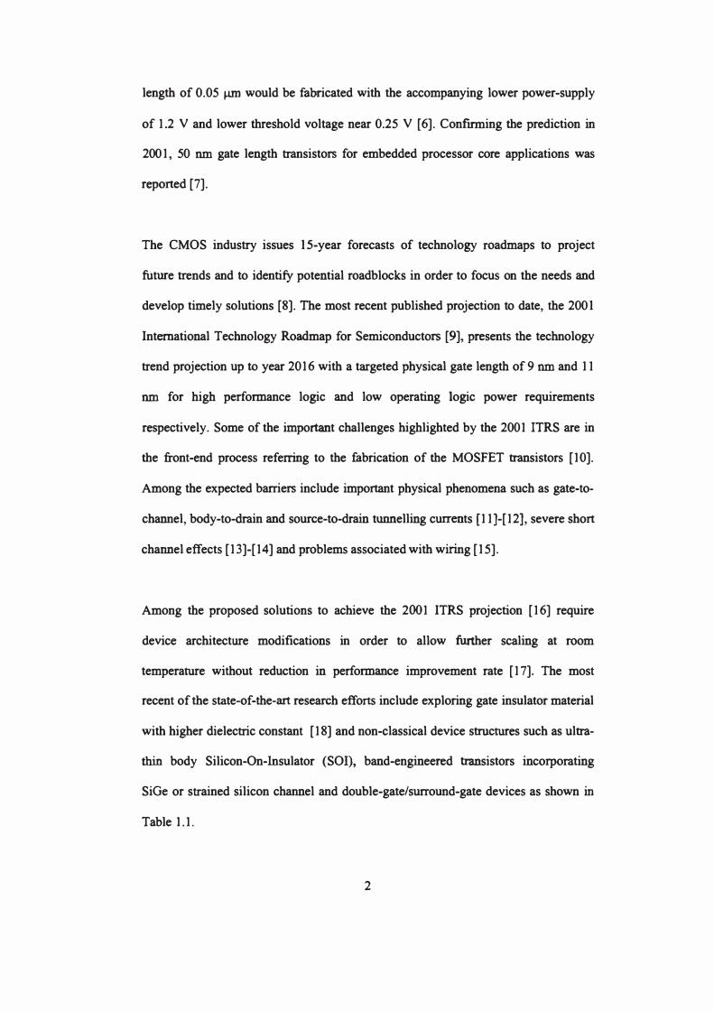
The CMOS industry issues IS-year forecasts of technology roadmaps to project
future trends and to identify potential roadblocks in order to focus on the needs and
develop timely solutions [8]. The most recent published projection to date, the 200 I
International Technology Roadmap for Semiconductors [9], presents the technology
trend projection up to year 2016 with a targeted physical gate length of 9 nm and 11
nm for high performance logic and low operating logic power requirements
respectively. Some of the important challenges highlighted by the 2001 ITRS are in
the front-end process referring to the fabrication of the MOSFET transistors [10].
Among the expected barriers include important physical phenomena such as gate-to
channel, body-to-drain and source-to-drain tunnelling currents (11J-[12J, severe short
channel effects [13]-[14] and problems associated with wiring [15].
Among the proposed solutions to achieve the 200 1 ITRS projection [16] require
device architecture modifications in order to allow further scaling at room
temperature without reduction in performance improvement rate [17]. The most
recent of the state-of-the-art research efforts include exploring gate insulator material
with higher dielectric constant [18] and non-classical device structures such as ultra
thin body Silicon-On-Insulator (SOl), band-engineered transistors incorporating
SiGe or strained silicon channel and double-gate/surround-gate devices as shown in
Table 1.1.
2

Table 1.1: Non-classical CMOS demonstrating device architectural modification aiming towards higher performance, higher transistor density and lower power
Device
ULTRA-THIN BODY SOl
BANDENGINEERED TRANSISOTR
VERTICAL TRANSISTOR
FINFET
DOUBLEGATE TRANSISTOR
dissipation. [19] Schematic Cross-Section
�.� . . . ,
L_. _____ _ .
Concept
Fully Depleted SOl
SiGe or Strained si Channel: bulk or SOl
Double-gate or surround-gate structtire
1.1.2 SOl CMOS Technology
AdvantaJl;es
-Improved subthreshold slope - Vt controllability
- Higher drive current - Bulk and SOl compatible
-Higher drive current -Lithography Independent Lg
-Higher drive current -Improved subthreshold slope -Improved short channel effect -Stacked NAND
-Higher drive current -Improved subthreshold slope -Improved short channel effect -Stacked NAND
The Silicon-On-Insulator MOSFET structure is one of many device architectural
modifications that have caught the attention of the CMOS industry since the late
1970s. The initial motivation towards the implementation of the structure is based on
its radiation hard properties, orienting the application of SOl devices towards space
and military purposes [20]. From the 80s onwards, the trend of SOl research is
directed towards low-voltage, low-power and high-speed properties and applications
[21].
SOl technology leads to steeper subthreshold slope, absence of CMOS latchup,
smaller off-state leakage current and reduced parasitic capacitances [22] leading to
3

improved speed-power products. Added advantage with SOl design is the versatility
of SOl structure design owing to additional physical parameters available for
manipulation towards optimized scaling [23]. Furthermore, SOl enables increased
chip functionality without the cost of major process equipment changes involving
higher resolution lithography tools. Contemporary SOl applications encompass
CMOS VLSl circuits, bipolar, power, Broadband LANs, micro-displays and MEMS
circuits [24].
Cost factor involved in SOl substrate fabrication is an obstruction for the migration
from bulk silicon to SOl technology. However, �cent developments have shown that
several semiconductor companies have begun to produce SOl devices commercially
in moderate volumes to benefit from the potential gains [25]. Further device design
making full use of the SOl substrate raises the possibility of reducing process steps
thus compensating the cost increase.
1.2 Research Objectives
Despite the fiscal implication being a barrier to the implementation of SOl research,
the interest of local microelectronics industry to venture the possibilities of SOl
technology would be inevitable. For this research effort, the research work is
implemented in MIMOS Berhad that runs the fIrSt wafer fabrication facility in
Malaysia. This is the first fabrication attempt involving SOl substrates on the
MIMOS production line. As SOl technology research work has yet to be reported in
Malaysia, the strategy adopted would be to implement an existing bulk silicon
technology to SOl substrates whilst maintaining its compatibility, only allowing
4