unit_iv.pdf
TRANSCRIPT

Input/Output Organization
Computer OrganizationComputer Organization
1

Overview
� Computer has ability to exchange data with other devices.
� Human-computer communicationComputer-computer communication� Computer-computer communication
� Computer-device communication� …
2

Accessing I/O Devices
3

Single Bus
Processor Memory
Bus
I/O device 1 I/O device n
Figure 4.1. A single-bus structure.4

Memory -Mapped I/O
� When I/O devices and the memory share the same address space, the arrangement is called memory-mapped I/O.
� Any machine instruction that can access memory can be used to transfer data to or from an I/O device.
Move DATAIN, R0Move R0, DATAOUT
� Some processors have special In and Out instructions to perform I/O transfer.
5
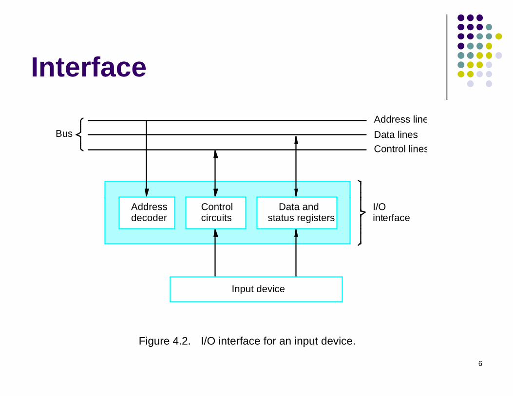
Interface
BusAddress lines
Data linesControl lines
I/O
Figure 4.2. I/O interface for an input device.
interfacedecoderAddress Data and
status registersControlcircuits
Input device
6

Program -Controlled I/O
� I/O devices operate at speeds that are very much different from that of the processor.
� Keyboard, for example, is very slow.� It needs to make sure that only after a � It needs to make sure that only after a
character is available in the input buffer of the keyboard interface; also, this character must be read only once.
7

Three Major Mechanisms
� Program-controlled I/O – processor polls the device.
� InterruptDirect Memory Access (DMA)� Direct Memory Access (DMA)
8
Interrupts
9

Overview
� In program-controlled I/O, the program enters a wait loop in which it repeatedly tests the device status. During the period, the processor is not performing any useful processor is not performing any useful computation.
� However, in many situations other tasks can be performed while waiting for an I/O device to become ready.
� Let the device alert the processor.10

Enabling and Disabling Interrupts
� Since the interrupt request can come at any time, it may alter the sequence of events from that envisaged by the programmer.
� Interrupts must be controlled.� Interrupts must be controlled.
11
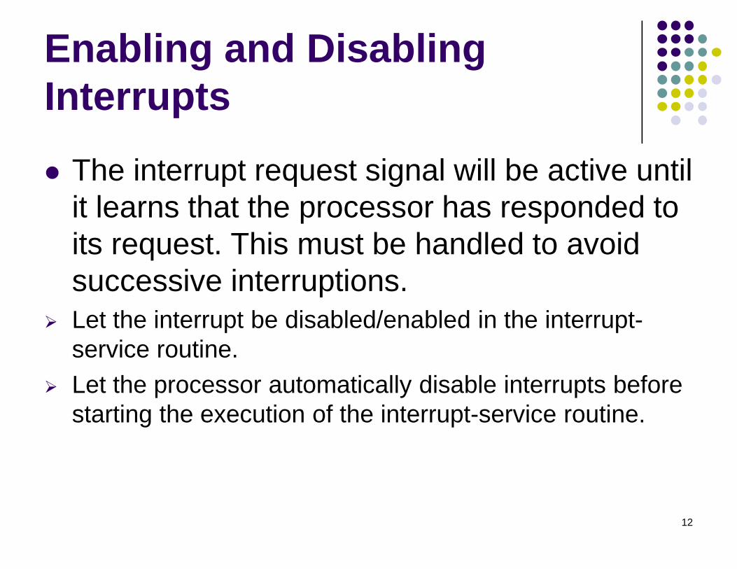
Enabling and Disabling Interrupts
� The interrupt request signal will be active until it learns that the processor has responded to its request. This must be handled to avoid successive interruptions.successive interruptions.� Let the interrupt be disabled/enabled in the interrupt-
service routine.� Let the processor automatically disable interrupts before
starting the execution of the interrupt-service routine.
12

Handling Multiple Devices� How can the processor recognize the device requesting an
interrupt?� Given that different devices are likely to require different
interrupt-service routines, how can the processor obtain the starting address of the appropriate routine in each case?
� (Vectored interrupts)� (Vectored interrupts)� Should a device be allowed to interrupt the processor while
another interrupt is being serviced?� (Interrupt nesting)� How should two or more simultaneous interrupt requests be
handled?� (Daisy-chain)
13

Vectored Interrupts
� A device requesting an interrupt can identify itself by sending a special code to the processor over the bus.
� Interrupt vector� Interrupt vector� Avoid bus collision
14

Interrupt Nesting� Simple solution: only accept one interrupt at a time, then disable
all others.� Problem: some interrupts cannot be held too long.� Priority structure
INTR1 I NTRp
Priority arbitration
Device 1 Device 2 Devicep
circuit
Pro
cess
or
Figure 4.7. Implementation of interrupt priority using individual
INTA1
INTR1 I NTRp
INTA p
interrupt-request and acknowledge lines. 15

Simultaneous Requests
(a) Daisy chain
Pro
cess
orDevice 2
I NTR
INTA
I NTR1
Device nDevice 1
Figure 4.8. Interrupt priority schemes.
(b) Arrangement of priority groups
Device Device
circuitPriority arbitration
Pro
cess
or
Device Device
INTR p
INTA1
INTA p
16

Controlling Device Requests
� Some I/O devices may not be allowed to issue interrupt requests to the processor.
� At device end, an interrupt-enable bit in a control register determines whether the control register determines whether the device is allowed to generate an interrupt request.
� At processor end, either an interrupt enable bit in the PS register or a priority structure determines whether a given interrupt request will be accepted.
17
Exceptions
� Recovery from errors� Debugging� Trace� Breakpoint� Breakpoint
� Privilege exception
18

Use of Interrupts in Operating Systems
� The OS and the application program pass control back and forth using software interrupts.
� Supervisor mode / user mode� Supervisor mode / user mode� Multitasking (time-slicing)� Process – running, runnable, blocked� Program state
19

Processor Examples
20

ConditionTrace
T S X N Z V C
012348101315
ConditionCodesInterrupt
PrioritySupervisor
Figure 4.14. Processor status register in the 68000 processor.
21

Main program
MOVE.L #LINE,PNTR Initialize buffer pointer.CLR EOL Clearend-of-line indicator.ORI.B #4,CONTROL Set bit KEN.MOVE #$100,SR Setprocessorpriority to1....
Interrupt-serviceroutine
READ MOVEM.L A0/D0, (A7) Save registersA0, D0 on stack.MOVEA.L PNTR,A0 Load addresspointer.MOVE.B DATAIN,D0 Get input character.
–
MOVE.B DATAIN,D0 Get input character.MOVE.B D0,(A0)+ Store it in memorybuffer.MOVE.L A0,PNTR Updatepointer.CMPI.B #$0D,D0 Check if CarriageReturn.BNE RTRNMOVE #1,EOL Indicateend of line.ANDI.B #$FB,CONTROL Clearbit KEN.
RTRN MOVEM.L (A7)+,A0/D0 Restore registersD0, A0.RTE
Figure 4.15. A 68000 interrupt-service routine to read an input line from a keyboard based on Figure 4.9.
22

Direct Memory Access
23

DMA
� Think about the overhead in both polling and interrupting mechanisms when a large block of data need to be transferred between the processor and the I/O device.
� A special control unit may be provided to allow transfer of a block of data directly between an transfer of a block of data directly between an external device and the main memory, without continuous intervention by the processor – direct memory access (DMA).
� The DMA controller provides the memory address and all the bus signals needed for data transfer, increment the memory address for successive words, and keep track of the number of transfers.
24

DMA Procedure
� Processor sends the starting address, the number of data, and the direction of transfer to DMA controller.
� Processor suspends the application program requesting DMA, starts DMA transfer, and starts another program.
� After the DMA transfer is done, DMA controller sends an interrupt signal to the processor.
� The processor puts the suspended program in the Runnable state.
25
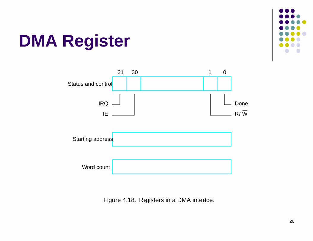
DMA Register
Done
IE
IRQ
Status and control
WR/
31 30 1 0
Starting address
Word count
Figure 4.18. Registers in a DMA interface.
26

System
memoryProcessor
System bus
Main
Figure 4.19. Use of DMA controllers in a computer system.
Keyboard
InterfaceNetwork
Disk/DMAcontroller Printer
DMAcontroller
DiskDisk
27

Memory Access
� Memory access by the processor and the DMA controller are interwoven.
� DMA device has higher priority.� Among all DMA requests, top priority is given � Among all DMA requests, top priority is given
to high-speed peripherals.� Cycle stealing� Block (burst) mode� Data buffer� Conflicts
28
Bus Arbitration
� The device that is allowed to initiate data transfers on the bus at any given time is called the bus master.
� Bus arbitration is the process by which the � Bus arbitration is the process by which the next device to become the bus master is selected and bus mastership is transferred to it.
� Need to establish a priority system.� Two approaches: centralized and distributed
29

Centralized Arbitration
Processor
BR
BBSY
DMAcontroller
1
DMAcontroller
2BG1 BG2
Figure 4.20. A simple arrangement for bus arbitration using a daisy chain.
30
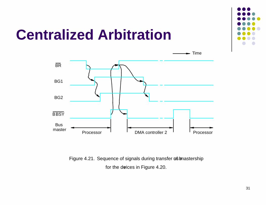
Centralized Arbitration
BG1
BG2
BR
Time
BBSY
Busmaster
Processor DMA controller 2 Processor
Figure 4.21. Sequence of signals during transfer of bus mastership
for the devices in Figure 4.20.
31

Distributed Arbitration
Vcc
Start-Arbitration
ARB0
ARB1
ARB2
ARB3
Figure 4.22. A distributed arbitration scheme.
Interface circuitfor device A
0 1 0 1 0 1 1 1
O.C.
Start-Arbitration
32

Buses
33

Overview
� The primary function of a bus is to provide a communications path for the transfer of data.
� A bus protocol is the set of rules that govern the behavior of various devices connected to the bus as to when to place information on the bus, assert control signals, etc.
� Three types of bus lines: data, address, control� The bus control signals also carry timing information.
� Bus master (initiator) / slave (target)
34

Synchronous Bus Timing
Bus clock
commandAddress and
Time
Figure 4.23. Timing of an input transfer on a synchronous bus.
Bus cycle
Data
t0 t1 t2
35

Synchronous Bus Detailed Timing
Bus clock
commandAddress and
Data
Seen by master tAM
tDM
Time
Figure 4.24. A detailed timing diagram for the input transfer of Figure 4.23.
Data
t0 t1 t2
commandAddress and
Seen by slavetAS
tDS
36
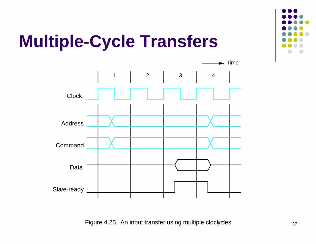
Multiple -Cycle Transfers
1 2 3 4
Clock
Address
Time
Figure 4.25. An input transfer using multiple clock cycles.
Address
Command
Data
Slave-ready
37

Asynchronous Bus – Handshaking Protocol for Input Operation
Master-ready
and commandAddress
Time
Figure 4.26. Handshake control of data transfer during an input operation.
Slave-ready
Data
Bus cycle
t1 t2 t3 t4 t5t0
38

Asynchronous Bus – Handshaking Protocol for Output Operation
Data
and commandAddress
Time
Figure 4.27. Handshake control of data transfer during an output operation.
Bus cycle
Master-ready
Slave-ready
t1 t2 t3 t4 t5t0
39

Discussion
� Trade-offs� Simplicity of the device interface� Ability to accommodate device interfaces that introduce
different amounts of delaydifferent amounts of delay� Total time required for a bus transfer� Ability to detect errors resulting from addressing a
nonexistent device or from an interface malfunction
� Asynchronous bus is simpler to design.� Synchronous bus is faster.
40

Interface Circuits
41

Function of I/O Interface
� Provide a storage buffer for at least one word of data;
� Contain status flags that can be accessed by the processor to determine whether the buffer is full or empty;
� Contain address-decoding circuitry to determine when it is being addressed by the processor;
� Generate the appropriate timing signals required by the bus control scheme;
� Perform any format conversion that may be necessary to transfer data between the bus and the I/O device.
42

Parallel Port
� A parallel port transfers data in the form of a number of bits, typically 8 or 16, simultaneously to or from the device.
� For faster communications� For faster communications
43

Parallel Port – Input Interface (Keyboard to Processor Connection)
Valid
Data
Keyboardswitches
Encoderand
debouncingcircuit
SIN
Data
Address
R /
Master-ready
W
DATAIN
Processor
ValidInput
interfaceSlave-ready
Figure 4.28. Keyboard to processor connection.
44

DATAIN
Keyboarddata
ValidStatusflag
Read-
1Slave-
Read-
SIN
Q7 D7
Q0 D0
D7
D0
data
status
ready
ready
A31
A1
A0
Addressdecoder
R/ W
Figure 4.29. Input interface circuit.
Master-
45

Parallel Port – Input Interface (Keyboard to Processor Connection)
46
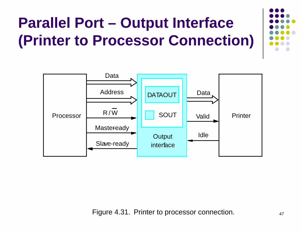
Parallel Port – Output Interface (Printer to Processor Connection)
CPU SOUT
Data
Address
R / ValidW
DataDATAOUT
PrinterProcessorCPU SOUT
Outputinterface
Master-eady
Slave-ready
Valid
Figure 4.31. Printer to processor connection.
PrinterProcessor
Idle
47

48

DATAIN
1
SIN
D7
D0
DATAOUT
Inputstatus
BusPA7
PA0
CA
PB7
PB0
CB1
CB2
SOUT
D1
Handshakecontrol
ReadySlave- 1
Ready
A31
A1
A0
Addressdecoder
R/ W
Figure 4.33. Combined input/output interface circuit.
A2
RS1
RS0
My-address
Master-
Ready
49

DATAIN
DATAOUT
DataDirection
P7
P0
D7
D0
Register
Register
select
Statusand
control
AcceptReady
R/WRS0RS1RS2
My-address
INTR
C1
C2
Figure 4.34. A general 8-bit parallel interface.50

Recall the Timing Protocol
1 2 3 4
Clock
Address
Time
Figure 4.25. An input transfer using multiple clock cycles.
Address
Command
Data
Slave-ready
51
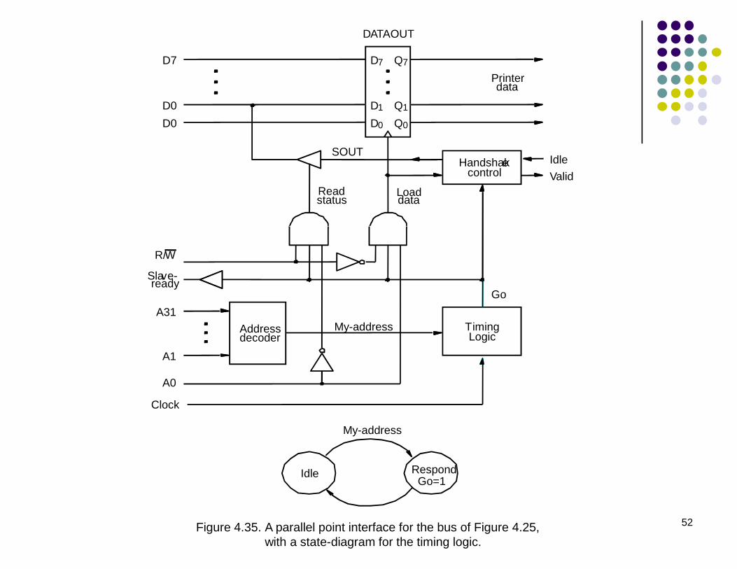
Handshakecontrol
DATAOUT
Printerdata
Idle
ValidRead Load
SOUT
ready
D7 Q7
D0 Q0
D7
D0
status data
D1 Q1D0
R/W
Slave-ready
A31
A1
A0
Addressdecoder
Figure 4.35. A parallel point interface for the bus of Figure 4.25,with a state-diagram for the timing logic.
TimingLogic
Clock
My-address
Idle Respond
My-address
Go
Go=1
52

Serial Port
� A serial port is used to connect the processor to I/O devices that require transmission of data one bit at a time.
� The key feature of an interface circuit for a � The key feature of an interface circuit for a serial port is that it is capable of communicating in bit-serial fashion on the device side and in a bit-parallel fashion on the bus side.
� Capable of longer distance communication than parallel transmission.
53

D7
D0
DATAIN
Input shift register Serialinput
I NTR
Chip andregisterselect
Statusand
control
Accept
Ready
R/W
RS0
RS1
My-address
Receiving clock
Transmission clock
Figure 4.37. A serial interface.
Output shift register
DATAOUT
Serialoutput
54

Standard I/O Interfaces
55

Overview� The needs for standardized interface signals and
protocols.� Motherboard� Bridge: circuit to connect two buses (processor Bridge: circuit to connect two buses (processor
bus to expansion bus)� Expansion bus - allows the CPU to talk to the
other devices in the computer and vice versa.� ISA(Industry Standard Architecture),
PCI(Peripheral Component Interconnect), SCSI(Small Computer System Interface), USB(Universal Serial Bus),… 56

memoryProcessor
Bridge
Processor bus
PCI bus
Main
memoryAdditional SCSI
controllerUSB
controllerISA
interfaceEthernetinterface
controllerCD-ROM
controllerDisk
Disk 1 Disk 2 ROMCD-
Video
Keyboard Game
diskIDE
SCSI bus
Figure 4.38. An example of a computer system using different interface standards.
57

ISA(Industry Standard Architecture)8-bit ISA BUS 16-bit ISA BUS
Bus width 8 - bit
Compatible with 8 bit ISA
Bus width 16 - bit
Compatible with 16 bit ISA
58
Pins 62
Power +5 V, -5 V, +12 V, -12 V
Clock 4.7727266 MHz
Pins 98
Power +5 V, -5 V, +12 V, -12 V
Clock 8.333333 MHz

PCI(Peripheral Component Interconnect)
� 32-Bit or 64-Bit address and data� 66 or 33 down to 0 MHz synchronous operation� Single or multiple bus masters� Bus parity error reporting
5 or 3.3 volt operation � 5 or 3.3 volt operation � Cache support� JTAG(Joint Test Action Group) testing
59

SCSI is:• a Specification• a Bus• a Protocol
SCSI(Small Computer System Interface)
• a Protocol

SCSI Terms
Initiator: A SCSI device that requests an operation to beperformed by another SCSI device.
Host Adapter: A Controller Board that translates host I/O requests into SCSI requests.
Target: A SCSI device that performs an operation as requested by an initiator.by an initiator.
Logical Unit: A Physical or Virtual device addressable through atarget.
LUN: Logical Unit Number. An encoded three-bit identifierfor the logical unit.

SCSI Device: A Host Adapter or Intelligent Peripheral whichcan be attached to a SCSI bus.
SCSI Address: The hex representation (0-7 or 0-F) of the uniqueaddress assigned to a SCSI device.
Connect: The function which occurs when an initiator
SCSI Terms
Connect: The function which occurs when an initiatorselects a target to begin an operation.
Disconnect: The function which occurs when a target releasescontrol of the SCSI bus, allowing it to go Bus Free.
Reconnect: The function which occurs when a targets selects aninitiator to continue an operation after a disconnect.

SCSI ConfigurationSingle Initiator, Single Target
Initiator
LUN0
TargetInitiatorSCSI Bus
LUN1
LUN2
Target

SCSI ConfigurationSingle Initiator, Multiple Targets
Initiator 7
Target 0T
SCSI Bus Target 1
Target n
SCSI Bus Terminator
T

SCSI ConfigurationMultiple Initiators, Multiple Targets
Initiator 7Target 0T
SCSI Bus Target 1
Target nInitiator 6
T

Single-Ended- Single Signal Level- 6m max. bus length- No Fast Timings- Uses Even bus pins only
Differential- Dual Signal Level- 25m max. bus length
0V
5V -SIG
TRUE
FALSE
TRUE = -SIG < 1.5V
SCSI Parallel Bus Types
- 25m max. bus length- Fast Timings- Uses all pins on bus
LVDS (SCSI-3+)- 3VDC Diff Bus
0V
5V -SIG
TRUE FALSE
+SIG
TRUE = -SIG < 1.5V
TRUE = +SIG > -SIG

USB(Universal Serial Bus)
� Universal Serial Bus is a new synchronous serialprotocol for low to medium speed data transmission� Full speed signaling 12 Mbs� Low Speed signaling 1.5 Mbs� Low Speed signaling 1.5 Mbs� Intended devices are keyboards, mice, joysticks,speakers; other low to medium speed IO devices
67