unit 4 application of boolean algebra
TRANSCRIPT

Department of Communication Engineering, NCTU 1
Unit 4 Application of BooleanAlgebra

Department of Communication Engineering, NCTU 2
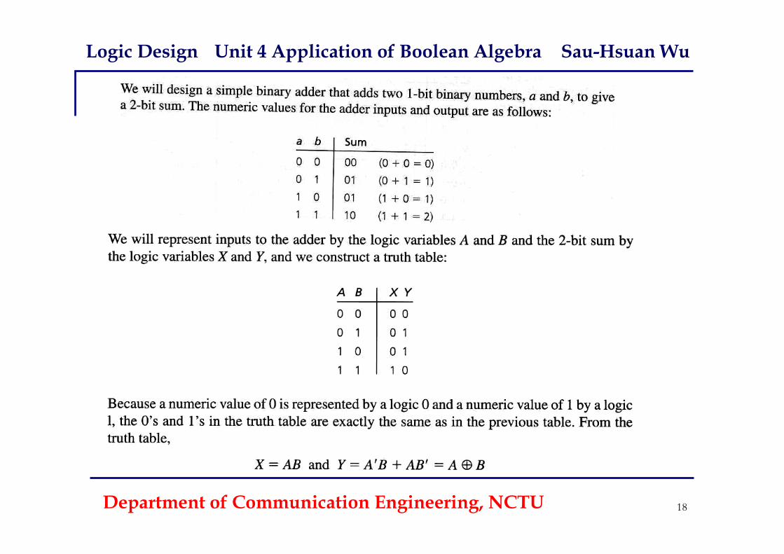
Logic Design Unit 4 Application of Boolean Algebra Sau-Hsuan Wu
Three main steps in designing a single-outputcombinational logic circuit Find a switching function that specifies the desired
behavior of the circuit Find a simplified algebraic expression for the function Realized the simplified function using available logic
elements Goals: How to specify circuit behaviors How to design a combinational logic circuit

Department of Communication Engineering, NCTU 3
4.1 Conversion of EnglishSentences to Boolean Equations

Department of Communication Engineering, NCTU 4
Logic Design Unit 4 Application of Boolean Algebra Sau-Hsuan Wu
For simple problems, go directly from a word descriptionof the desired circuit behavior to an algebra expression Mary watches TV if it is Monday night and she has
finished her homework.F = A˙B
The alarm will ring iffthe alarm switch is turned on
and the door is not closed,or it is after 6 P.M.and the window is not closed.
Z = AB' + CD'

Department of Communication Engineering, NCTU 5
4.2 Combinational Logic DesignUsing a Truth Table

Department of Communication Engineering, NCTU 6
Logic Design Unit 4 Application of Boolean Algebra Sau-Hsuan Wu
In general, a truth table to design logic circuits First, list a true table E.g.
Derive an algebraic expression for f from the table
f = A'BC + AB'C' + AB'C + ABC' + ABC (4-1)= A+BC

Department of Communication Engineering, NCTU 7
Logic Design Unit 4 Application of Boolean Algebra Sau-Hsuan Wu
In stead of writing f in terms of the 1’s of the function,we may also write f in terms of the 0’s of the function E.g.
f = (A+B+C)(A+B+C')(A+B'+C) (4-3)= (A+B)(A+B'+C) = A + BC

Department of Communication Engineering, NCTU 8
4.3 Minterm and MaxtermExpansions

Department of Communication Engineering, NCTU 9
Logic Design Unit 4 Application of Boolean Algebra Sau-Hsuan Wu
Each term in (4-1) is referred to as a minterm f = A'BC + AB'C' + AB'C + ABC' + ABC (4-1)
A function written as a sum of minterms is referred toas a minterm expansion or a standard SOP
Each term in (4-3) is referred to as a maxterm f = (A+B+C)(A+B+C')(A+B'+C) (4-3)
A function written as a product of maxterms is referredto as a maxterm expansion or a standard POS

Department of Communication Engineering, NCTU 10
Logic Design Unit 4 Application of Boolean Algebra Sau-Hsuan Wu
A minterm of n variables is a product of n literals inwhich each variable appears exactly once in either true orcomplemented form
The decimal notation of minterm expansione.g. f = m (3,4,7)

Department of Communication Engineering, NCTU 11
Logic Design Unit 4 Application of Boolean Algebra Sau-Hsuan Wu
A maxterm of n variables is a sum of n literals in whicheach variable appears exactly once in either true orcomplemented form
The decimal notation of maxterm expansionE.g. f = M(0,,2)
Given the minterm or maxterm expansions for f , theminterm or maxterm expansions for the complement of fare easy to obtain E.g.
Or
0 1 2
3 4 5 6 7
(0,1,2)
(3,4,5,6,7)
f m m m m
f M M M M M M
0 1 2 0 1 2 0 1 2( )f M M M M M M m m m

Department of Communication Engineering, NCTU 12
Logic Design Unit 4 Application of Boolean Algebra Sau-Hsuan Wu
A general switching expansion can be converted to aminterm or a maxterm expansion either using a truth tableor algebraically
For algebraic method, first write the expansion as a sumof products and then introduce the missing variables ineach term by applying the theorem X + X’=1
Example f(a,b,c,d) = a’(b’+d) + acd’ 1> SOP: f= a’b’+a’d+acd’ Introduce missing variables
f= a’b’(c+c’)(d+d’)+a’(b+b’)(c+c’)d+ a(b+b’)cd’= a’b’c’d’+a’b’c’d+a’b’cd’+a’b’cd+a’b’c’d+a’b’cd
+ a’b’cd + a’bcd + abcd’+ ab’cd’= m (0,1,2,3,5,7,10,14)

Department of Communication Engineering, NCTU 13
Logic Design Unit 4 Application of Boolean Algebra Sau-Hsuan Wu
General minterm and maxterm expansions A general minterm expansion
f = a0m0 + a1m1+ + a7m7 = ai miai = 0 or 1
mi is not present if ai = 0 A general maxterm expansion
f = (ã0 + M0)(ã1 + M1) (ã7 + M7) = (ãi + Mi)ãi = 0 or 1
Mi is not present if ãi = 1
Equality ai mi = (ãi + Mi)

Department of Communication Engineering, NCTU 14
4.5 Incompletely SpecifiedFunctions

Department of Communication Engineering, NCTU 15
Logic Design Unit 4 Application of Boolean Algebra Sau-Hsuan Wu
A large system is usually divided into many subcircuits.The output of module 1 may not generate all possiblecombinations for the input variables of module 2.
In this case, we don’t care these specific combinationswhen designing the switch circuit for F

Department of Communication Engineering, NCTU 16
Logic Design Unit 4 Application of Boolean Algebra Sau-Hsuan Wu
When realizing the function, the don‘t care terms can beassigned 0’s or 1’s If both X’s are assigned 0
F = A'B'C' + A'BC +ABC = A'B'C' + BC
If first X is assigned 1 and the second 0F = A'B'C' + A'B'C + A'BC +ABC = A'B' + BC
If we assign 1 to both X’sF = A'B'C' + A'B'C + A'BC + ABC' + ABC
= A'B' + BC + AB

Department of Communication Engineering, NCTU 17
4.5 Examples of Truth TableConstruction
Department of Communication Engineering, NCTU 18
Logic Design Unit 4 Application of Boolean Algebra Sau-Hsuan Wu

Department of Communication Engineering, NCTU 19
Logic Design Unit 4 Application of Boolean Algebra Sau-Hsuan Wu
Error detector for 6-3-1-1 binary-coded-decimal digits

Department of Communication Engineering, NCTU 20
Logic Design Unit 4 Application of Boolean Algebra Sau-Hsuan Wu
Switching Expression

Department of Communication Engineering, NCTU 21
4.5 Design of Binary Adders

Department of Communication Engineering, NCTU 22
Logic Design Unit 4 Application of Boolean Algebra Sau-Hsuan Wu
Design a 4-bit binary ripple carry adder Approach 1:
construct a truth table
Approach 2: cascade 4 1-bit Full Adders

Department of Communication Engineering, NCTU 23
Logic Design Unit 4 Application of Boolean Algebra Sau-Hsuan Wu
Construct the true table for1-bit full adder
Find the switching expressions
( ) ( )
( ) ( )
in in in in
in in in in
in in in
Sum X Y C X YC XY C XYC
X Y C YC X Y C YC
X Y C X Y C X Y C
( ) ( ) ( )out in in in in
in in in in in in
in in
C X YC XY C XYC XYC
X YC XYC XY C XYC XYC XYC
YC XC XY

Department of Communication Engineering, NCTU 24
Logic Design Unit 4 Application of Boolean Algebra Sau-Hsuan Wu
Implement the functions with logic gates
Overflow occurs if adding two positive numbers gives anegative result, or adding two negative numbers results ina positive number
3 3 3 3 3 3V A B S A B S

Department of Communication Engineering, NCTU 25
Logic Design Unit 4 Application of Boolean Algebra Sau-Hsuan Wu
The pros and cons of ripple carry adder Simple in concept The carry output at stage i+1
Ci+1 = XiYi + (Xi + Yi) Ci
The carries propagate like a ripple and introduce circuitdelays : C0 C1 C2 Ci+1
Ci+1 = f (Xi,Yi, Ci) = f (Xi,Yi,Xi-1,Yi-1,Ci-1) = Alternative: Carry lookahead adder To avoid circuit delays due to the propagation of
carries Express Ci+1 in terms of C0 and {X0,Yi Xi,Yi} only

Department of Communication Engineering, NCTU 26
Logic Design Unit 4 Application of Boolean Algebra Sau-Hsuan Wu
Re-write the output carry at the ith stage as Ci+1 = gi + pi Ci
The carry-generate function: gi = XiYi
The carry-propagate function pi = Xi + Yi
Expression the carry bit in terms of gi and pi
C1 = g0 + p0 C0
C2 = g1 + p1 C1 = g1 + p1 g0 + p1 p0 C0
C3 = g2 + p2 C2 = g2 + p2 g1 + p2 p1 g0 + p2 p1 p0 C0
Ci = gi + pi gi-1 + pi pi-1gi-2 + + pi pi-1 pi-2 g0
+ pi pi-1 pi-2 p0C0

Department of Communication Engineering, NCTU 27
Logic Design Unit 4 Application of Boolean Algebra Sau-Hsuan Wu
The circuit implementation of 4-bit carry lookahead adder
block
Carry lookahead network

Department of Communication Engineering, NCTU 28
Logic Design Unit 4 Application of Boolean Algebra Sau-Hsuan Wu
For adders with higher number of bits, the carrylookahead network can get quite large in terms of gatesand gate inputs. This also presents a limitation in therealization of a large high speed adder
How to circumvent this problem? Cascade 4-bit carry lookahead adders to form a lager adder

Department of Communication Engineering, NCTU 29
Logic Design Unit 4 Application of Boolean Algebra Sau-Hsuan Wu
Partition the operands into blocksE.g.C8 = g7 + p7 g6 + p7 p6g5 + p7 p6p5g4 + p7 p6p5p4g3 +
p7 p6p5p4p3g2 + p7 p6p5p4p3p2g1 + p7 p6p5p4p3p2p1g0+p7 p6p5p4p3p2p1p0C0
= g7 + p7 g6 + p7 p6g5 + p7 p6p5g4 +p7 p6p5p4 (g3 + p3g2 + p3p2g1 + p3p2p1g0) +p7 p6p5p4(p3p2p1p0C0)
= G1 + P1G0 + P1P0C0G1= g7 + p7 g6 + p7 p6g5 + p7 p6p5g4P1 = p7 p6p5p4G0= g3 + p3g2 + p3p2g1 + p3p2p1g0P0 = p3p2p1p0

Department of Communication Engineering, NCTU 30
Logic Design Unit 4 Application of Boolean Algebra Sau-Hsuan Wu
Define a 4-bit carry lookahead generator asG= g3 + p3g2 + p3p2g1 + p3p2p1g0P = p3p2p1p0