um10876 nhs31xx user manual - mouser electronics · um10876 nhs31xx user manual rev. 1 — 30...
TRANSCRIPT
UM10876NHS31xx User manualRev. 1 — 30 November 2016 User manual
Document informationInfo ContentKeywords ARM Cortex-M0+, NHS3100, NHS3152, NHS3153, Cold chain,
Temperature, Temperature logging, Drug adherence, Therapy adherence, NFC
Abstract User manual for the NHS31xx family of wired or wireless sensor node ICs

<Document ID>UM10876 All information provided in this document is subject to legal disclaimers. © NXP Semiconductors N.V. 2016. All rights reserved.
User manual Rev. 1 — 30 November 2016 2 of 234
Contact informationFor more information, please visit: http://www.nxp.com
For sales office addresses, please send an email to: [email protected]
NXP Semiconductors UM10876NHS31xx User manual
Revision historyRev Date Description
1 20161130 Initial version
<Document ID>UM10876 All information provided in this document is subject to legal disclaimers. © NXP Semiconductors N.V. 2016. All rights reserved.
User manual Rev. 1 — 30 November 2016 3 of 234
NXP Semiconductors UM10876NHS31xx User manual
1. Introductory information
1.1 IntroductionThe NHS31xx are a family of ICs optimized for monitoring and logging. With their embedded NFC interface, internal temperature sensor and direct battery connection, they support effective system solutions with a minimal number of external components.
The embedded ARM Cortex-M0+ offers flexibility to the users of these ICs to implement their own dedicated solution. The NHS31xx family contains multiple features, like a selectable CPU frequency of up to 8 MHz and various power-down modes for ultra-low-power consumption.
Users can program this NHS31xx family with the industry-wide standard solutions for ARM Cortex-M0+ processors.
Peripheral components include an ultra-low-power RTC, I2C-bus interface, SPI interface with SSP features, NFC wireless interface and up to 12 general-purpose I/O pins.
Depending on the chip variant, other features include a temperature sensor, specific interfaces for capacitive, resistive and current measurements, and a 12-bit ADC/DAC. There are also specific analog interfaces for interfacing with photodiodes and LEDs.
1.2 AttributesNote: not all features are available in all family members.
• System:– ARM Cortex-M0+ processor, running at frequencies of up to 8 MHz– ARM Cortex-M0+ built-in Nested Vectored Interrupt Controller (NVIC)– ARM Serial Wire Debug (SWD)– System tick timer– Fast (single-cycle) multiplier– Support for wake-up interrupt controller– Vector Table remapping possible– IC reset input
• Debug options:– Serial Wire Debug with two watchpoint comparators and four breakpoint
comparators– Halting debug
• Memory:– 32 kB on-chip flash programming memory– 4 kB on-chip EEPROM of which 256 bytes can be write protected– 8 kB SRAM
• Analog peripherals available, depending on variant:– Temperature sensor with 0.3 C absolute temperature accuracy between 0 C
and 40 C, and 0.5 °C in the range 40 C to +85 C
<Document ID>UM10876 All information provided in this document is subject to legal disclaimers. © NXP Semiconductors N.V. 2016. All rights reserved.
User manual Rev. 1 — 30 November 2016 4 of 234
NXP Semiconductors UM10876NHS31xx User manual
– Capacitance-to-digital converter– Current-to-digital converter– SAR ADC– DAC for generating external biasing voltages– 8-bit 20 mA current DAC on 4 pins
• Flexible analog on-chip switch:– Each of the 6 analog I/O pins can be dynamically connected to the on-chip
converters.– Measuring 6 voltages connected to the 6 analog pins is possible using
time-division multiplexing• Digital peripherals:
– Up to 12 General-Purpose Input Output (GPIO) pins with configurable pull-up/pull-down resistors
– GPIO pins that can be used as edge and level sensitive interrupt sources– High-current drivers/sinks (20 mA) on four pins– High-current drivers/sinks (20 mA) on two I2C-bus pins– Programmable watchdog timer (WDT)
• Communication interfaces:– NFC/RFID ISO 14443 type A interface– SPI controller with SSP features and with FIFO and multi-protocol capabilities– I2C-bus interface supporting full I2C-bus specification and Fast-mode with a data
rate of 400 kbit/s with multiple address recognition and monitor mode• Clock generation:
– 8 MHz internal RC oscillator trimmed to 2 % accuracy that is used as the system clock
– Timer oscillator operating at 32 kHz linked to On/Off Timer unit, driving the real-time clock timer
• Power control:– Supply voltage range: 1.72 V to 3.6 V– Passive powering via NFC field possible– Integrated Power Management Unit (PMU) for fine-grained control of power
consumption– Four reduced power modes: Sleep, Deep-sleep, Deep power-down and Battery-off– Power gating for each analog peripheral for ultra-low-power operation– < 50 nA current consumption with battery power switch open– Power-On Reset (POR)
• Unique device serial number for identification• Wide operating temperature range• Available in HVQFN24 and WLCSP25 package (see Table 2).
<Document ID>UM10876 All information provided in this document is subject to legal disclaimers. © NXP Semiconductors N.V. 2016. All rights reserved.
User manual Rev. 1 — 30 November 2016 5 of 234
NXP Semiconductors UM10876NHS31xx User manual
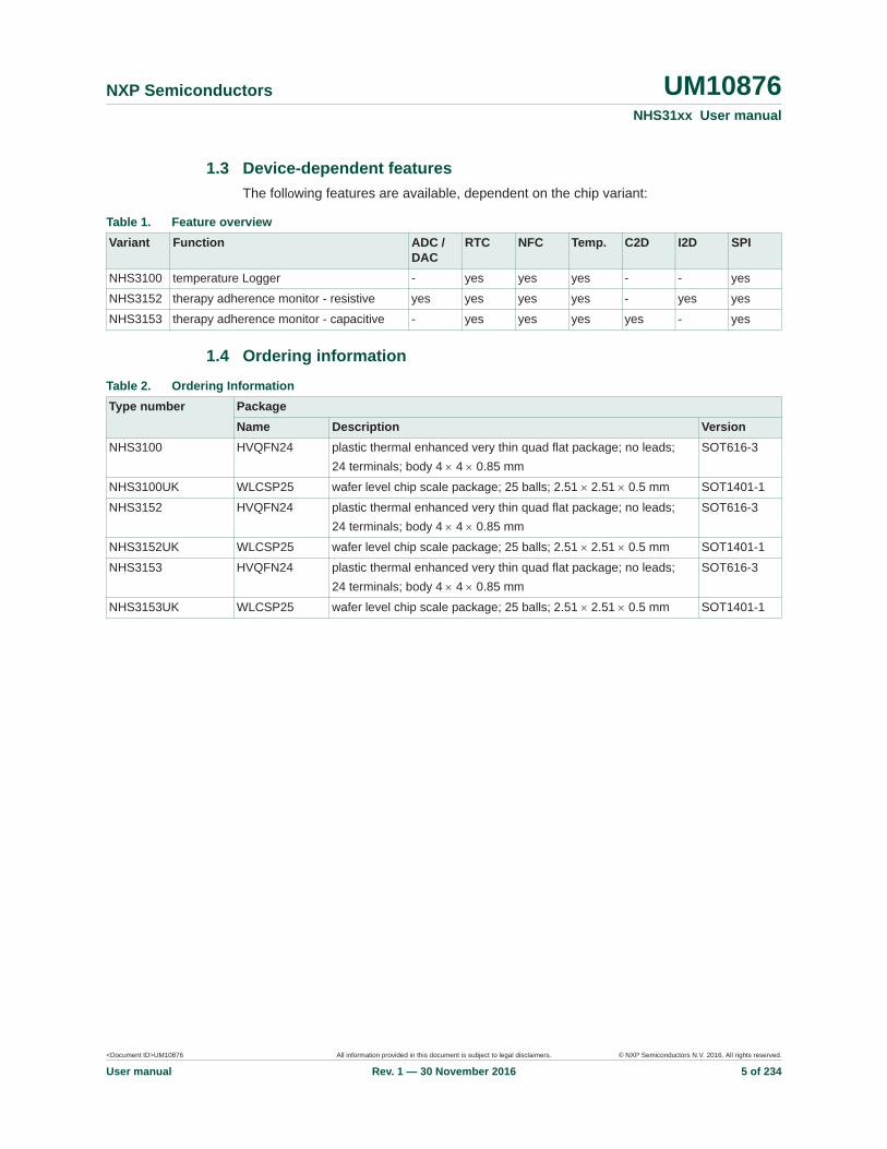
1.3 Device-dependent featuresThe following features are available, dependent on the chip variant:
1.4 Ordering information
Table 1. Feature overviewVariant Function ADC /
DACRTC NFC Temp. C2D I2D SPI
NHS3100 temperature Logger - yes yes yes - - yes
NHS3152 therapy adherence monitor - resistive yes yes yes yes - yes yes
NHS3153 therapy adherence monitor - capacitive - yes yes yes yes - yes
Table 2. Ordering InformationType number Package
Name Description VersionNHS3100 HVQFN24 plastic thermal enhanced very thin quad flat package; no leads;
24 terminals; body 4 4 0.85 mmSOT616-3
NHS3100UK WLCSP25 wafer level chip scale package; 25 balls; 2.51 2.51 0.5 mm SOT1401-1
NHS3152 HVQFN24 plastic thermal enhanced very thin quad flat package; no leads;24 terminals; body 4 4 0.85 mm
SOT616-3
NHS3152UK WLCSP25 wafer level chip scale package; 25 balls; 2.51 2.51 0.5 mm SOT1401-1
NHS3153 HVQFN24 plastic thermal enhanced very thin quad flat package; no leads;24 terminals; body 4 4 0.85 mm
SOT616-3
NHS3153UK WLCSP25 wafer level chip scale package; 25 balls; 2.51 2.51 0.5 mm SOT1401-1

<Document ID>UM10876 All information provided in this document is subject to legal disclaimers. © NXP Semiconductors N.V. 2016. All rights reserved.
User manual Rev. 1 — 30 November 2016 6 of 234
NXP Semiconductors UM10876NHS31xx User manual
1.5 Block diagrams
NHS3100 Temperature logger
NHS3152 for therapy adherence using resistive sensing
Fig 1. NHS3100 block diagram
POWERPADS
PADS
WAKE-UPTIMER
32 kHz FRO
CLOCKSHOP
EXTERNALPOWERSWITCH
INTERNALPOWER
SWITCHES
POR
LDO (1.6 V)
LDO (1.2 V)8 MHz FRO
MFIO(DIGITAL)
HIGHDRIVE
DIGITALSWITCHMATRIX I2C-BUS SPI GPIO
32 kB FLASH
4 kB EEPROM
ARM M0+
AHB-APB BRIDGE
8 kB SRAM
PMU
NFC/RFID
FLASHCONTROL
EEPROMCONTROL
TIMERS WATCHDOG SYSCONFIG
IOC
ON
FIG
TEMPERATURESENSOR
I2C-BUS
aaa-015348
Fig 2. NHS3152 block diagram
PADS
WAKE-UPTIMER
32 kHz FRO
CLOCKSHOP
EXTERNALPOWERSWITCH
INTERNALPOWER
SWITCHES
POR
LDO (1.6 V)
LDO (1.2 V)8 MHz FRO
DIGITALSWITCHMATRIX I2C
I2D
SPI GPIO32 kB FLASH
4 kB EEPROM
ARM M0+
AHB-APB BRIDGE
8 kB SRAM
PMU
NFC/RFID
FLASHCONTROL
EEPROMCONTROL
TIMERS WATCHDOG SYSCONFIG
DAC-ADCIOC
ON
FIG
TEMPERATURESENSOR
ANALOGSWITCHMATRIX
aaa-016914
APIO(ANALOG)
HIGHDRIVE
MFIO(DIGITAL)
POWERPADS
I2C
<Document ID>UM10876 All information provided in this document is subject to legal disclaimers. © NXP Semiconductors N.V. 2016. All rights reserved.
User manual Rev. 1 — 30 November 2016 7 of 234
NXP Semiconductors UM10876NHS31xx User manual
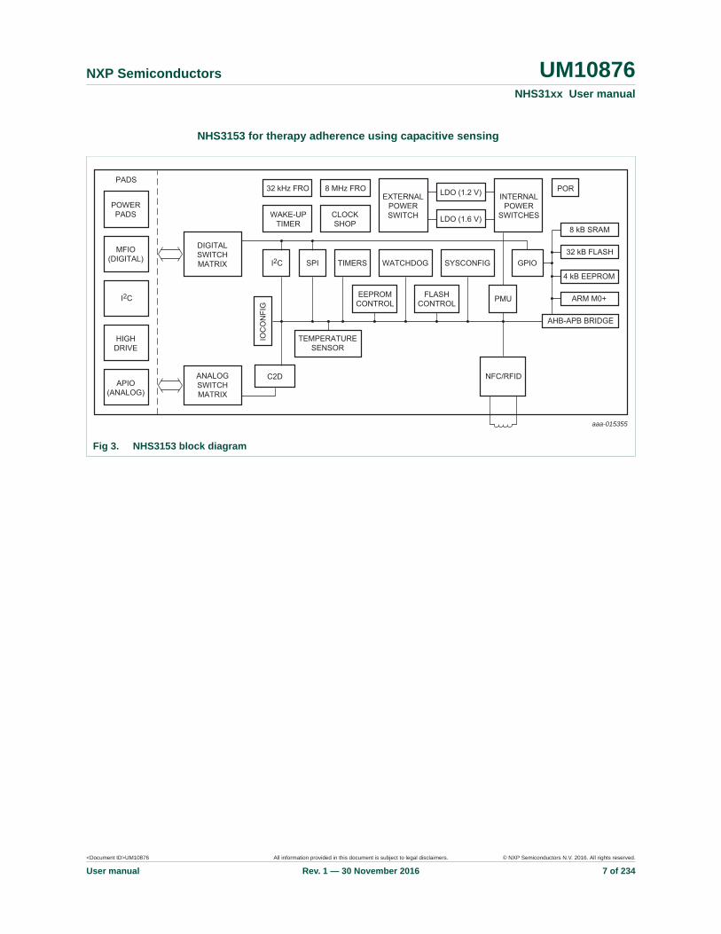
NHS3153 for therapy adherence using capacitive sensing
Fig 3. NHS3153 block diagram
PADS
WAKE-UPTIMER
32 kHz FRO
CLOCKSHOP
EXTERNALPOWERSWITCH
INTERNALPOWER
SWITCHES
POR
LDO (1.6 V)
LDO (1.2 V)8 MHz FRO
DIGITALSWITCHMATRIX I2C
C2D
SPI GPIO32 kB FLASH
4 kB EEPROM
ARM M0+
AHB-APB BRIDGE
8 kB SRAM
PMU
NFC/RFID
FLASHCONTROL
EEPROMCONTROL
TIMERS WATCHDOG SYSCONFIGIO
CO
NFI
G
TEMPERATURESENSOR
ANALOGSWITCHMATRIX
APIO(ANALOG)
HIGHDRIVE
MFIO(DIGITAL)
POWERPADS
I2C
aaa-015355

<Document ID>UM10876 All information provided in this document is subject to legal disclaimers. © NXP Semiconductors N.V. 2016. All rights reserved.
User manual Rev. 1 — 30 November 2016 8 of 234
NXP Semiconductors UM10876NHS31xx User manual
1.6 ARM Cortex-M0+ core configurationThe ARM Cortex-M0+ core operates at frequencies up to 8 MHz. Integrated in the core are the NVIC and Serial Wire Debug with four breakpoints and two watch points. It supports a single-cycle I/O enabled port (IOP) for fast GPIO access.
The specific firmware loaded on the non-volatile memory of the device determines its behavior.
The ARM Cortex-M0+ processor is described in detail in Ref. 3. For the NHS31xx family, the ARM Cortex-M0+ core is configured as follows:
• System options:– Nested Vectored Interrupt Controller (NVIC) which is included and supports up to
32 interrupts– Fast (single-cycle) multiplier– System tick timer– Support for wake-up interrupt controller– Vector Table remapping register– Reset all registers present– No memory protection unit– No single-cycle I/O port– Instruction fetch width, mostly 32-bit wide– Data endianness: little endian
• Debug options– Serial Wire Debug is included with two watchpoint comparators and four
breakpoint comparators– Halting debug is supported
1.7 Memory mapFigure 4 shows the memory and peripheral address space.
Peripheral accesses can only be done as 32-bit accesses on addresses divisible by 4. An implication of this is that word and halfword registers must be accessed at the same time. For example, it is not possible to read or write the upper bytes of a word register separately.

<Document ID>UM10876 All information provided in this document is subject to legal disclaimers. © NXP Semiconductors N.V. 2016. All rights reserved.
User manual Rev. 1 — 30 November 2016 9 of 234
NXP Semiconductors UM10876NHS31xx User manual
1.7.1 Memories
1.7.1.1 SRAM (0x1000 0000 to 0x1000 1FFF)The NHS31xx contains a total of 8 kB on-chip static RAM memory configured as 256 2 4 32 bit. The SRAM supports byte-level access (BWE=8).
1.7.1.2 Flash (0x0000 0000 to 0x0000 7FFF)The NHS31xx contains a 32 kB Flash memory of which 30 kB can be used as program and data memory.
The flash is organized in 32 sectors of 1 kB. Each sector consists of 16 rows of 16 32-bit words.
(1) Note: Not all registers on the APB block are present on all the chip variants
Fig 4. NHS31xx family memory map
aaa-016649
0
1
2
3
4
5
6-12
13
14
15
16
17
18
19-20
21
23
22
25
24
0x4000 0000
0x4000 4000
0x4000 8000
0x4000 C0000x5001 00000x5000 FFFC
0x5000 0000
0x501F FFFF 0x4001 4000
0x4003 4000
0x4003 C000
0x4003 8000
0x4004 0000
0x4004 4000
0x4004 8000
0x4005 4000
0x4005 8000
0x4005 C000
0x4006 0000
l2C
Watchdog timer
(reserved)
16-bit counter-timer
(reserved)
32-bit counter-timer
(reserved)
EEPROM controller
PMU
Flash controller
SPI/SSP
I/O configuration
System configuration
(reserved)
RTC timer
(reserved)
RFID/NFC
Cap-to-digital
Temperature sensor
27-31
26
(reserved)
Current-to-digital
0x4006 4000
0x4006 8000
0x0000 7FFF
0x0000 0000
0x0FFF FFFF
0x000 8000
0x2FFF FFFF
0x1000 20000x1000 1FFF
0x1000 0000
0x3000 10000x3000 0FFF
0x3000 0000
0x3FFF FFFF
0x4007 FFFF
0x4000 0000
0x4FFF FFFF
0x4008 0000
0x501F FFFF
0x5000 0000
0x5020 0000
0xE01F FFFF
0xE000 00000xDFFF FFFF
0xFFFF FFFF
0xE010 0000
GPIO PIO0
(reserved)(reserved)
(reserved)
(reserved)
(reserved)
(reserved)
(reserved)
private peripheral bus
AHB peripherals
APB peripherals
4 kB EEPROM
8 kB SRAM
32 kB on-chip Flash
AHB Peripherals
Active interrupt vectors
APB Peripherals
0x0000 0000
0x0000 00BF
Active interrupt vectors
<Document ID>UM10876 All information provided in this document is subject to legal disclaimers. © NXP Semiconductors N.V. 2016. All rights reserved.
User manual Rev. 1 — 30 November 2016 10 of 234
NXP Semiconductors UM10876NHS31xx User manual
1.7.1.3 EEPROM (0x3000 0000 to 0x3000 0FFF)The NHS31xx contains a 4 kB EEPROM. This EEPROM is organized in 64 rows of 32 16-bit words. Of these rows, the last four contain calibration and test data and are locked. This data is either used by the boot loader after reset, or made accessible to the application via firmware API.
<Document ID>UM10876 All information provided in this document is subject to legal disclaimers. © NXP Semiconductors N.V. 2016. All rights reserved.
User manual Rev. 1 — 30 November 2016 11 of 234
NXP Semiconductors UM10876NHS31xx User manual
2. Product feature overview
2.1 About this chapterNHS31xx is available in several different variants to suit different applications. This chapter gives an overview of the principle components of each variant.
2.2 General descriptionAll ICs share flexibility, standard adherence and ultra-low-power features:
• The embedded ARM Cortex-M0+ offers flexibility and processing power to the users of this IC. It enables them to implement their own dedicated solution, including decision making on the IC itself. The ICs contain multiple features including various power-down modes and a selectable CPU frequency up to 8 MHz for ultra-low-power consumption.
• Users can program this IC via SWD using industry-wide standard solutions for ARM Cortex-M0+ processors, or via NFC and the freely provided NFC program downloader. Note: Programming via NFC can only be done once.
2.2.1 NHS3100 for cold chain monitoring and therapy adherenceThe NHS3100 is an IC optimized for temperature monitoring and logging. The embedded NFC interface, allows fully NFC-forum standards-compliant communication, internal temperature sensing and direct battery connection. It supports an effective system solution with a minimal of external components.
2.2.2 NHS3152 for therapy adherence using resistive sensingThe NHS3152 is an IC optimized for realizing therapy adherence monitoring and logging solutions. The embedded NFC interface allows fully NFC-forum standards-compliant communication, a resistive network sensing interface, an internal temperature sensor and direct battery connection. The NHS3152 enables the making of an effective system solution, supporting a single layer foil implementation, for pill usage monitoring. The NHS3152 works either battery-powered or NFC-powered.
2.2.3 NHS3153 for therapy adherence using capacitive sensingThe NHS3153 is an IC optimized for realizing therapy adherence monitoring and logging solutions. The embedded NFC interface allows fully NFC-forum standards-compliant communication, a capacitive network sensing interface, an internal temperature sensor and direct battery connection. The NHS3153 allows the creation of an effective system solution, supporting a single layer foil implementation, for pill usage monitoring. The NHS3153 works either battery-powered or NFC-powered.
<Document ID>UM10876 All information provided in this document is subject to legal disclaimers. © NXP Semiconductors N.V. 2016. All rights reserved.
User manual Rev. 1 — 30 November 2016 12 of 234
NXP Semiconductors UM10876NHS31xx User manual
3. Pinning
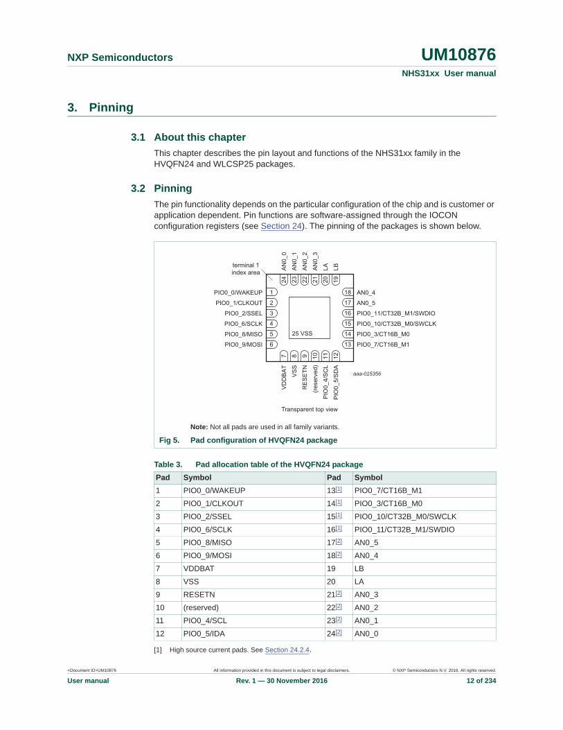
3.1 About this chapterThis chapter describes the pin layout and functions of the NHS31xx family in the HVQFN24 and WLCSP25 packages.
3.2 PinningThe pin functionality depends on the particular configuration of the chip and is customer or application dependent. Pin functions are software-assigned through the IOCON configuration registers (see Section 24). The pinning of the packages is shown below.
[1] High source current pads. See Section 24.2.4.
Note: Not all pads are used in all family variants.
Fig 5. Pad configuration of HVQFN24 package
Table 3. Pad allocation table of the HVQFN24 packagePad Symbol Pad Symbol1 PIO0_0/WAKEUP 13[1] PIO0_7/CT16B_M1
2 PIO0_1/CLKOUT 14[1] PIO0_3/CT16B_M0
3 PIO0_2/SSEL 15[1] PIO0_10/CT32B_M0/SWCLK
4 PIO0_6/SCLK 16[1] PIO0_11/CT32B_M1/SWDIO
5 PIO0_8/MISO 17[2] AN0_5
6 PIO0_9/MOSI 18[2] AN0_4
7 VDDBAT 19 LB
8 VSS 20 LA
9 RESETN 21[2] AN0_3
10 (reserved) 22[2] AN0_2
11 PIO0_4/SCL 23[2] AN0_1
12 PIO0_5/IDA 24[2] AN0_0
aaa-015356
Transparent top view
PIO0_7/CT16B_M1
PIO0_8/MISO
PIO0_9/MOSI
PIO0_3/CT16B_M0
PIO0_6/SCLK PIO0_10/CT32B_M0/SWCLK
PIO0_2/SSEL PIO0_11/CT32B_M1/SWDIO
PIO0_1/CLKOUT AN0_5
PIO0_0/WAKEUP AN0_4
25 VSS
VD
DB
AT
VS
S
RE
SE
TN
(res
erve
d)
PIO
0_4/
SC
L
PIO
0_5/
SD
A
AN
0_0
AN
0_1
AN
0_2
AN
0_3
LA LBterminal 1index area
6 13
5 14
4 15
3 16
2 17
1 187 8 9 10 11 12
24 23 22 21 20 19

<Document ID>UM10876 All information provided in this document is subject to legal disclaimers. © NXP Semiconductors N.V. 2016. All rights reserved.
User manual Rev. 1 — 30 November 2016 13 of 234
NXP Semiconductors UM10876NHS31xx User manual
[2] Only used in variants with analog I/O. In other variants, they can be tied to ground.
Table 4. Pad description of the HVQFN24 packagePad Symbol Type DescriptionSupply7 VDDBAT supply positive supply voltage
8 VSS supply ground
GPIO[1]
1 PIO0_0 I/O GPIO
WAKEUP I Deep power-down mode wake-up pad[2]
2 PIO0_1 I/O GPIO
CLKOUT O clock output
3 PIO0_2 I/O GPIO
SSEL I SPI/SSP SSEL select line
14 PIO0_3 I/O GPIO
CT16B_M0 O 16-bit timer match output 0
11 PIO0_4 I/O GPIO[3]
SCL I/O I2C SCL clock line
12 PIO0_5 I/O GPIO[3]
SDA I/O I2C SDA data line
4 PIO0_6 I/O GPIO
SCLK I/O SPI/SSP serial clock line
13 PIO0_7 I/O GPIO
CT16B_M1 O 16-bit timer match output 1
5 PIO0_8 I/O GPIO
MISO O SPI/SSP master-in slave-out line
6 PIO0_9 I/O GPIO
MOSI I SPI/SSP master-out slave-in line
15 PIO0_10 I/O GPIO
CT32B_M0 O 32-bit timer match output 0
SWCLK I ARM SWD clock
16 PIO0_11 I/O GPIO
CT32B_M1 O 32-bit timer match output 1
SWDIO I/O ARM SWD I/O
Analog I/O[4][5]
24 AN0_0 A to AN0_BUS0
23 AN0_1 A to AN0_BUS1
22 AN0_2 A to AN0_BUS2
21 AN0_3 A to AN0_BUS3
18 AN0_4 A to AN0_BUS4
17 AN0_5 A to AN0_BUS5
Radio20 LA A NFC antenna/coil terminal A
<Document ID>UM10876 All information provided in this document is subject to legal disclaimers. © NXP Semiconductors N.V. 2016. All rights reserved.
User manual Rev. 1 — 30 November 2016 14 of 234
NXP Semiconductors UM10876NHS31xx User manual
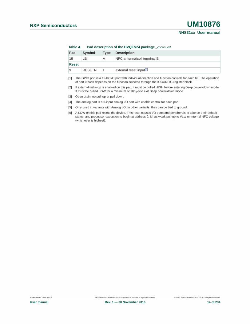
[1] The GPIO port is a 12-bit I/O port with individual direction and function controls for each bit. The operationof port 0 pads depends on the function selected through the IOCONFIG register block.
[2] If external wake-up is enabled on this pad, it must be pulled HIGH before entering Deep power-down mode. It must be pulled LOW for a minimum of 100 s to exit Deep power-down mode.
[3] Open drain, no pull-up or pull down.
[4] The analog port is a 6-input analog I/O port with enable control for each pad.
[5] Only used in variants with Analog I/O. In other variants, they can be tied to ground.
[6] A LOW on this pad resets the device. This reset causes I/O ports and peripherals to take on their defaultstates, and processor execution to begin at address 0. It has weak pull-up to VBAT or internal NFC voltage(whichever is highest).
19 LB A NFC antenna/coil terminal B
Reset9 RESETN I external reset input[6]
Table 4. Pad description of the HVQFN24 package _continued
Pad Symbol Type Description

<Document ID>UM10876 All information provided in this document is subject to legal disclaimers. © NXP Semiconductors N.V. 2016. All rights reserved.
User manual Rev. 1 — 30 November 2016 15 of 234
NXP Semiconductors UM10876NHS31xx User manual
[1] High source current balls. See Section 24.2.4.[2] Only used in variants with Analog I/O. In other variants, they can be tied to ground.
Note: Not all balls are used in all family variants.
Fig 6. Ball configuration of WLCSP25 package
Table 5. Ball allocation table of the WLCSP25 packageBall Symbol Ball SymbolA1 VDDBAT C4[1] PIO0_7/CT16B_M1
A2 VSS C5[1] PIO0_11/CT32B_M1/SWDIO
A3 RESETN D1 PIO0_0/WAKEUP
A4 PIO0_4/SCL D2 PIO0_1/CLKOUT
A5 PIO0_5/SDA D3[2] AN0_2
B1 PIO0_8/MISO D4[2] AN0_4
B2 PIO0_9/MOSI D5[2] AN0_5
B3 (reserved) E1[2] AN0_0
B4[1] PIO0_3/CT16B_M0 E2[2] AN0_1
B5[1] PIO0_10/CT32B_M0/SWCLK E3[2] AN0_3
C1 PIO0_2/SSEL E4 LA
C2 PIO0_6/SCLK E5 LB
C3 VSS - -
A
B
C
D
E
1 2 3 4 5
Transparent top view
<Document ID>UM10876 All information provided in this document is subject to legal disclaimers. © NXP Semiconductors N.V. 2016. All rights reserved.
User manual Rev. 1 — 30 November 2016 16 of 234
NXP Semiconductors UM10876NHS31xx User manual
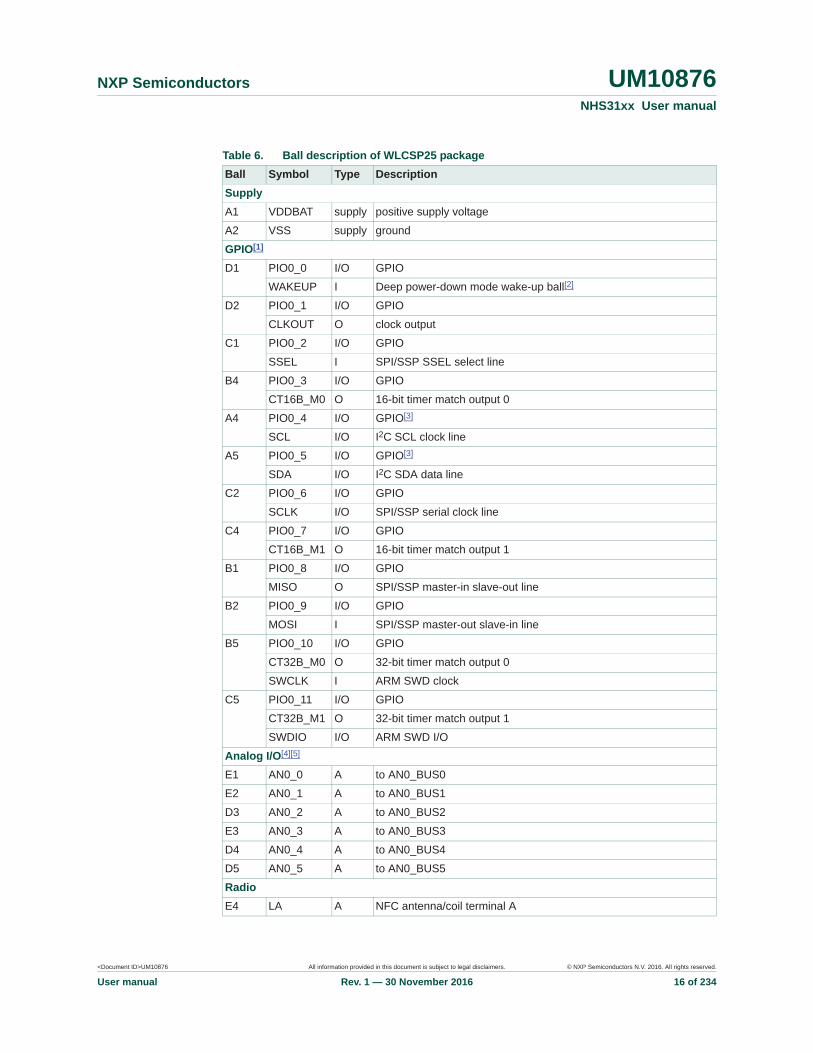
Table 6. Ball description of WLCSP25 packageBall Symbol Type DescriptionSupplyA1 VDDBAT supply positive supply voltage
A2 VSS supply ground
GPIO[1]
D1 PIO0_0 I/O GPIO
WAKEUP I Deep power-down mode wake-up ball[2]
D2 PIO0_1 I/O GPIO
CLKOUT O clock output
C1 PIO0_2 I/O GPIO
SSEL I SPI/SSP SSEL select line
B4 PIO0_3 I/O GPIO
CT16B_M0 O 16-bit timer match output 0
A4 PIO0_4 I/O GPIO[3]
SCL I/O I2C SCL clock line
A5 PIO0_5 I/O GPIO[3]
SDA I/O I2C SDA data line
C2 PIO0_6 I/O GPIO
SCLK I/O SPI/SSP serial clock line
C4 PIO0_7 I/O GPIO
CT16B_M1 O 16-bit timer match output 1
B1 PIO0_8 I/O GPIO
MISO O SPI/SSP master-in slave-out line
B2 PIO0_9 I/O GPIO
MOSI I SPI/SSP master-out slave-in line
B5 PIO0_10 I/O GPIO
CT32B_M0 O 32-bit timer match output 0
SWCLK I ARM SWD clock
C5 PIO0_11 I/O GPIO
CT32B_M1 O 32-bit timer match output 1
SWDIO I/O ARM SWD I/O
Analog I/O[4][5]
E1 AN0_0 A to AN0_BUS0
E2 AN0_1 A to AN0_BUS1
D3 AN0_2 A to AN0_BUS2
E3 AN0_3 A to AN0_BUS3
D4 AN0_4 A to AN0_BUS4
D5 AN0_5 A to AN0_BUS5
RadioE4 LA A NFC antenna/coil terminal A

<Document ID>UM10876 All information provided in this document is subject to legal disclaimers. © NXP Semiconductors N.V. 2016. All rights reserved.
User manual Rev. 1 — 30 November 2016 17 of 234
NXP Semiconductors UM10876NHS31xx User manual
[1] The GPIO port is a 12-bit I/O port with individual direction and function controls for each bit. The operation of port 0 balls depends on the function selected through the IOCONFIG register block.
[2] If external wake-up is enabled on this ball, it must be pulled HIGH before entering Deep power-down mode. It must be pulled LOW for a minimum of 100 s to exit Deep power-down mode.
[3] Open drain, no pull-up or pull down.
[4] The analog port is a 6-input analog I/O port with enable control for each pad.
[5] Only used in variants with Analog I/O. In other variants, they can be tied to ground.
[6] A LOW on this ball resets the device. This reset causes I/O ports and peripherals to take on their default states, and processor execution to begin at address 0. It has weak pull-up to VBAT or internal NFC voltage (whichever is highest).
E5 LB A NFC antenna/coil terminal B
ResetA3 RESETN I external reset input[6]
Table 6. Ball description of WLCSP25 package _continued
Ball Symbol Type Description

<Document ID>UM10876 All information provided in this document is subject to legal disclaimers. © NXP Semiconductors N.V. 2016. All rights reserved.
User manual Rev. 1 — 30 November 2016 18 of 234
NXP Semiconductors UM10876NHS31xx User manual
4. System configuration (SYSCON)
4.1 General descriptionThe system configuration block is at APB 0x4004 8000. It controls oscillators, start logic, and clock generation of the NHS31xx. It contains registers controlling power on/off of the peripherals and a register to remap the ARM vector table to a selectable location in Flash or SRAM.
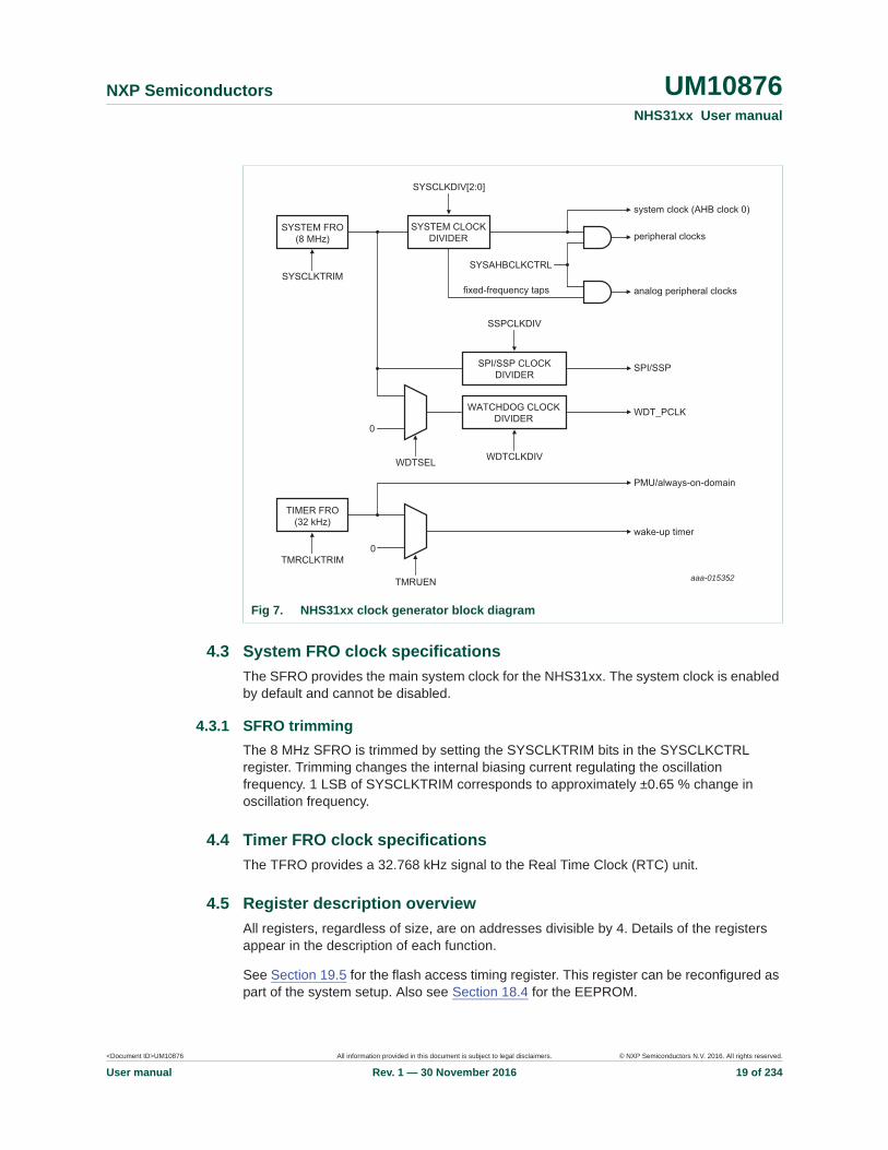
4.2 Clock generationThe NHS31xx clock generator unit (CGU) includes two independent RC oscillators. These oscillators are the System Free-Running Oscillator (SFRO) and the Timer Free-RunningOscillator (TFRO).
The SFRO is a current-controlled oscillator and runs at 8 MHz. The system clock is derived from it. The system clock can be set to 8 MHz, 4 MHz, 2 MHz, 1 MHz, 500 kHz, 250 kHz, 125 kHz or 62.5 kHz with the SYSCLKCTRL system configuration register (see Table 10). The default system clock operating frequency is 500 kHz to minimize dynamic current consumption during the boot cycle. Note: some features are not available when using the lower clock speeds.
The TFRO runs at 32.768 kHz and is the clock source for the Real-Time Clock (RTC) unit and the power management unit. The TMRCLKCTRL configuration register similarly controls it.
Following reset, the NHS31xx starts operating from the SFRO at the default 500 kHz clock frequency. The user can change the system clock frequency by setting the SYSCLKSEL. The SFRO cannot be disabled.
The SYSAHBCLKCTRL register gates the system clock to the various peripherals and memories. The SPI unit has an individual clock divider to derive the serial clock from the SFRO. The watchdog timer unit also has an individual clock divider.
The analog parts of the analog-to-digital converters receive a fixed clock frequency, irrespective of the system clock divider settings. The digital part uses the APB clock. The analog part of the temperature sensor receives 2 MHz, the ADC/DAC receives 8 MHz, and the other peripherals 1 MHz.
<Document ID>UM10876 All information provided in this document is subject to legal disclaimers. © NXP Semiconductors N.V. 2016. All rights reserved.
User manual Rev. 1 — 30 November 2016 19 of 234
NXP Semiconductors UM10876NHS31xx User manual
4.3 System FRO clock specificationsThe SFRO provides the main system clock for the NHS31xx. The system clock is enabled by default and cannot be disabled.
4.3.1 SFRO trimmingThe 8 MHz SFRO is trimmed by setting the SYSCLKTRIM bits in the SYSCLKCTRL register. Trimming changes the internal biasing current regulating the oscillation frequency. 1 LSB of SYSCLKTRIM corresponds to approximately ±0.65 % change in oscillation frequency.
4.4 Timer FRO clock specificationsThe TFRO provides a 32.768 kHz signal to the Real Time Clock (RTC) unit.
4.5 Register description overviewAll registers, regardless of size, are on addresses divisible by 4. Details of the registers appear in the description of each function.
See Section 19.5 for the flash access timing register. This register can be reconfigured as part of the system setup. Also see Section 18.4 for the EEPROM.
Fig 7. NHS31xx clock generator block diagram
aaa-015352
SYSTEM FRO(8 MHz)
SYSTEM CLOCKDIVIDER
SYSCLKTRIMfixed-frequency taps
system clock (AHB clock 0)
peripheral clocks
analog peripheral clocks
SPI/SSP
WDT_PCLK
wake-up timer
PMU/always-on-domain
SYSCLKDIV[2:0]
SPI/SSP CLOCKDIVIDER
SSPCLKDIV
WDTCLKDIV
SYSAHBCLKCTRL
TIMER FRO(32 kHz)
TMRCLKTRIM
TMRUEN
WATCHDOG CLOCKDIVIDER
WDTSEL
0
0

<Document ID>UM10876 All information provided in this document is subject to legal disclaimers. © NXP Semiconductors N.V. 2016. All rights reserved.
User manual Rev. 1 — 30 November 2016 20 of 234
NXP Semiconductors UM10876NHS31xx User manual
Table 7. Register overview system configuration control block - SYSCON (base address 0x4004 8000)Name Access Address
offsetDescription Reset
valueReference
SYSMEMREMAP R/W 0x000 system memory remap 0x0000 0000 Table 8
PRESETCTRL R/W 0x004 peripheral reset control 0x0000 0000 Table 9
- - 0x008 - 0x01C
(reserved) - -
SYSCLKCTRL R/W 0x020 system clock control register 0x0002 0008 Table 10
SYSCLKUEN R/W 0x024 system clock update enable 0x0000 0000 Table 12
- - 0x028 - 0x02C
(reserved) - -
SYSRSTSTAT R/W 0x030 system reset status register 0x0000 0000 Table 13
- - 0x034 - 0x078
(reserved) - -
SYSAHBCLKCTRL R/W 0x080 AHB clock control 0x0001 C007 Table 14
- - 0x084 - 0x090
(reserved) - -
SSPCLKDIV R/W 0x094 SPI/SSP clock divider 0x0000 0000 Table 15
- - 0x098 - 0x0CC
(reserved) - -
WDTCLKSEL R/W 0x0D0 watchdog timer clock selector 0x0000 0000 Table 16
WDTCLKUEN R/W 0x0D4 watchdog timer clock update enable 0x0000 0000 Table 17
WDTCLKDIV R/W 0x0D8 watchdog timer clock divider 0x0000 0000 Table 18
- - 0x0DC - 0x0E4
(reserved) - -
CLKOUTEN R/W 0x0E8 CLKOUT enable 0x0000 0000 Table 19
- - 0x0EC - 0x150
(reserved) - -
SYSTCKCAL R/W 0x154 system tick counter calibration 0x0000 0004 Table 20
- - 0x210 - 0X230
(reserved) - -
STARTAPRP0 R/W 0x200 start logic edge control register 0 0x0000 0000 Table 21
STARTERP0 R/W 0x204 start logic signal enable register 0 0x0000 0000 Table 22
STARTRSRP0CLR R/W 0x204 start logic reset register 0 0x0000 0000 Table 23
STARTSRP0 R 0x20C start logic status register 0 0x0000 0000 Table 24
- - 0x210 - 0X230
(reserved) - -
PDAWAKECFG R/W 0x234 Flash address mapping after wake-up from Deep-sleep mode
0x0000 0000 Table 25
PDRUNCFG R/W 0x238 power-down configuration register 0x0000 003E Table 26
- - 0x23C - 0x3EC
(reserved) - -
DEVICE_ID R 0x3F4 - - Table 27

<Document ID>UM10876 All information provided in this document is subject to legal disclaimers. © NXP Semiconductors N.V. 2016. All rights reserved.
User manual Rev. 1 — 30 November 2016 21 of 234
NXP Semiconductors UM10876NHS31xx User manual
4.5.1 System memory remap register (SYSMEMREMAP)The system memory remap register contains the addresses of the ARM interrupt vectors. Valid addresses are on 1024 byte boundaries in Flash or SRAM. The first 192 addresses (0 to 191) are remapped to the locations indicated below.
4.5.2 Peripheral reset control register (PRESETCTRL)This register allows software to reset some peripherals. Writing a logic 0 to the bits resets the corresponding peripheral. Writing a logic 1 de-asserts the reset.
Remark: Before accessing the SPI and I2C peripherals, write a logic 1 to this register. This action ensures that the reset signals to the SPI and I2C are de-asserted.
4.5.3 System clock control register (SYSCLKCTRL)The system clock control register controls the analog part of the internal 8 MHz oscillator as well as the system clock divider.
Table 8. SYSMEMREMAP register (address 0x4004 8000) bit descriptionBit Symbol Value Description After boot0 map - interrupt vector remap 0
0 interrupt vectors reside in Flash
1 interrupt vectors reside in SRAM
5:1 offset - system memory remap offset 00000b
00000b interrupt vectors in flash or remapped to SRAM but not offset
00001b - 00111b
interrupt vectors offset in flash or SRAM to 1 K word segment
01000b - 11111b
interrupt vectors offset in flash to 1 K word segment 8 to 31
31:6 - - (reserved) 0
Table 9. PRESETCTRL register (address 0x4004 8004) bit descriptionBit Symbol Value Description After boot0 SSP_RST_N - SPI/SSP reset control 0
0 resets the SPI peripheral
1 SPI reset de-asserted
1 I2C_RST_N - I2C-bus reset control 0
0 resets the I2C-bus peripheral
1 I2C-bus reset de-asserted
2 EE_RST_N - EEPROM NVMC reset control 1
0 resets the EEPROM NVMC controller
1 reset de-asserted
3 NFC_RST_N - NFC shared memory reset control 1
0 resets the NFC shared memory
1 reset de-asserted
31:4 - - (reserved) 0
<Document ID>UM10876 All information provided in this document is subject to legal disclaimers. © NXP Semiconductors N.V. 2016. All rights reserved.
User manual Rev. 1 — 30 November 2016 22 of 234
NXP Semiconductors UM10876NHS31xx User manual
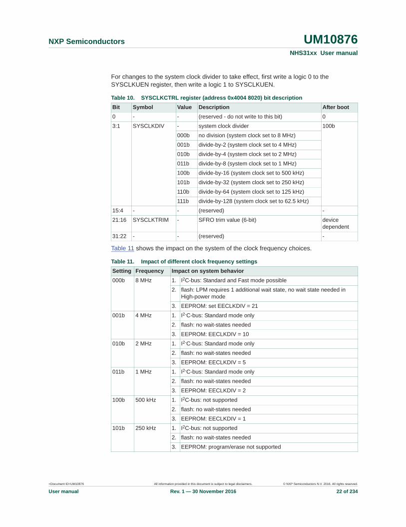
For changes to the system clock divider to take effect, first write a logic 0 to the SYSCLKUEN register, then write a logic 1 to SYSCLKUEN.
Table 11 shows the impact on the system of the clock frequency choices.
Table 10. SYSCLKCTRL register (address 0x4004 8020) bit descriptionBit Symbol Value Description After boot0 - - (reserved - do not write to this bit) 0
3:1 SYSCLKDIV - system clock divider 100b
000b no division (system clock set to 8 MHz)
001b divide-by-2 (system clock set to 4 MHz)
010b divide-by-4 (system clock set to 2 MHz)
011b divide-by-8 (system clock set to 1 MHz)
100b divide-by-16 (system clock set to 500 kHz)
101b divide-by-32 (system clock set to 250 kHz)
110b divide-by-64 (system clock set to 125 kHz)
111b divide-by-128 (system clock set to 62.5 kHz)
15:4 - - (reserved) -
21:16 SYSCLKTRIM - SFRO trim value (6-bit) device dependent
31:22 - - (reserved) -
Table 11. Impact of different clock frequency settingsSetting Frequency Impact on system behavior000b 8 MHz 1. I2C-bus: Standard and Fast mode possible
2. flash: LPM requires 1 additional wait state, no wait state needed in High-power mode
3. EEPROM: set EECLKDIV = 21
001b 4 MHz 1. I2-C-bus: Standard mode only
2. flash: no wait-states needed
3. EEPROM: EECLKDIV = 10
010b 2 MHz 1. I2-C-bus: Standard mode only
2. flash: no wait-states needed
3. EEPROM: EECLKDIV = 5
011b 1 MHz 1. I2-C-bus: Standard mode only
2. flash: no wait-states needed
3. EEPROM: EECLKDIV = 2
100b 500 kHz 1. I2C-bus: not supported
2. flash: no wait-states needed
3. EEPROM: EECLKDIV = 1
101b 250 kHz 1. I2C-bus: not supported
2. flash: no wait-states needed
3. EEPROM: program/erase not supported
<Document ID>UM10876 All information provided in this document is subject to legal disclaimers. © NXP Semiconductors N.V. 2016. All rights reserved.
User manual Rev. 1 — 30 November 2016 23 of 234
NXP Semiconductors UM10876NHS31xx User manual
4.5.4 System clock update enable register (SYSCLKUEN)This register updates the clock source of the system with the new input clock after the SYSCLKCTRL register has been written to. For the update to take effect, first write a logic 0 to the SYSCLKUEN register and then write a logic 1 to SYSCLKUEN.
4.5.5 System reset status register (SYSRSTSTAT)The SYSRSTSTAT register shows the source of the latest reset event. The bits are cleared by writing a value to the register. The POR event clears all other bits in this register. However, if another reset signal - for example EXTRST - remains asserted after the POR signal is negated, then its bit is set to detected.
[1] POR and EXTRST trigger full system reset.
110b 125 kHz 1. I2C: not supported
2. flash: no wait-states needed
3. EEPROM: program/erase not supported
111b 62.5 kHz 1. I2C: not supported
2. flash: no wait-states needed
3. EEPROM: program/erase not supported
Table 11. Impact of different clock frequency settings _continued
Setting Frequency Impact on system behavior
Table 12. SYSCLKUEN register (address 0x4004 8024) bit descriptionBit Symbol Value Description Reset
value0 ENA - enable system clock source update 0
0 no update
1 update clock source and clock divisor
31:1 - - (reserved) 0
Table 13. SYSRSTSTAT register (address 0x4004 8030) bit descriptionBit Symbol Value Description Reset
value0 POR [1] - POR reset status 0
0 no POR detected
1 POR detected
1 EXTRST [1] - status of external RESETN pin 0
0 no RESETN event detected
1 external reset detected
2 WDT [2] - status of the Watchdog reset 0
0 no WDT reset detected
1 WDT reset detected
3 SYSRST [3] - status of software system reset (ARM AIRCR register SYSRESETREQ bit was set)
0
0 no software reset detected
1 software reset detected
31:4 - - (reserved) -

<Document ID>UM10876 All information provided in this document is subject to legal disclaimers. © NXP Semiconductors N.V. 2016. All rights reserved.
User manual Rev. 1 — 30 November 2016 24 of 234
NXP Semiconductors UM10876NHS31xx User manual
[2] If the debugger is not active, then WDT triggers full system reset.
[3] SYSRST triggers a reset of the ARM core (the peripheral registers are not reset).
4.5.6 AHB clock control registerThe SYSAHBCLKCTRL register enables the clocks to individual system and peripheral blocks. The system clock provides the clock for the AHB to APB bridge, the AHB matrix, the ARM Cortex-M0+, the SYSCON block, and the PMU. This clock cannot be disabled.
Table 14. SYSAHBCLKCTRL register (address 0x4004 8080) bit descriptionBit Symbol Value Description Reset
value0 - 1 (reserved) 1
1 - - (reserved) -
2 RAM - enable clock for RAM 1
0 disable
1 enable
4:3 FLASHREG / FLASHARRAY
- enable clock for Flash register interface and array access
0b11
0b00 disable
0b01 enable
0b10 enable
0b11 enable
5 I2C - enable clock for I2C-bus 0
0 disable
1 enable
6 GPIO - enable clock for GPIO 0
0 disable
1 enable
7 SPISSP - enable clock for SPI/SSP 0
0 disable
1 enable
8 CT16B - enable clock for 16-bit timer 0
0 disable
1 enable
9 CT32B - enable clock for 32-bit timer 0
0 disable
1 enable
10 RTC - enable clock for RTC (APB side only, TFRO directly clocks the timer unit, as set by TMRCLKCTRL register).
0
0 disable
1 enable
11 WDT - enable clock for watchdog timer 0
0 disable
1 enable
<Document ID>UM10876 All information provided in this document is subject to legal disclaimers. © NXP Semiconductors N.V. 2016. All rights reserved.
User manual Rev. 1 — 30 November 2016 25 of 234
NXP Semiconductors UM10876NHS31xx User manual
4.5.7 SPI/SSP clock divider control register (SSPCLKDIV)This register configures the SPI peripheral clock SPI_PCLK. The SPI_PCLK can be shut down by setting the DIV bits to logic 0.
4.5.8 Watchdog timer clock source selection register (WDTCLKSEL)
This register selects the clock source for the watchdog timer. The WDTCLKUEN register must be toggled from logic 0 to logic 1 for the update to take effect.
12 TSEN - enable clock for temperature sensor 0
0 disable
1 enable
13 C2D - enable clock for Capacitance-to-Digital converter 0
0 disable
1 enable
14 - - (reserved)
15 I2D - enable clock for Current-to-Digital converter 0
0 disable
1 enable
16 ADC/DAC - enable clock for ADC/DAC converter 0
0 disable
1 enable
17 - - (reserved)
18 IOCON - enable clock for I/O configuration block 1
0 disable
1 enable
20:19 EEREG / EEARRAY
- enable clock for EEPROM register interface and array access
0b11
0b00 disable
0b01 enable
0b10 enable
0b11 enable
31:21 - - (reserved) 0
Table 14. SYSAHBCLKCTRL register (address 0x4004 8080) bit description _continued
Bit Symbol Value Description Reset value
Table 15. SSPCLKDIV register (address 0x4004 8094) bit descriptionBit Symbol Value Description Reset
value7:0 DIV - SPI_CLK clock divider values: (0) disable, (1) equal to
SFRO frequency (even 2-254) divide-by-DIV0
31:8 - - (reserved) 0

<Document ID>UM10876 All information provided in this document is subject to legal disclaimers. © NXP Semiconductors N.V. 2016. All rights reserved.
User manual Rev. 1 — 30 November 2016 26 of 234
NXP Semiconductors UM10876NHS31xx User manual
4.5.9 Watchdog timer clock update enable register (WDTCLKUEN)This register updates the clock source of the watchdog timer with the new input source after the WDTCLKSEL register has been written to. In order for the update to take effect at the input of the watchdog timer, the following procedure must be applied:
1. Write a logic 0 to the WDTCLKUEN register2. Write a logic 1 to WDTCLKUEN to preset the value3. Write a logic 0 again to apply the value
The 0-1-0 pulse length should be longer than the period of the actual and selected clock sources.
4.5.10 Watchdog timer clock divider register (WDTCLKDIV)This register determines the divider values for the watchdog clock wdt_clk. For the update to take effect at the input of the watchdog timer, a 1-0-1 sequence has to be written to register WDTCLKEN. See Section 4.5.9
When the division factor is set to 0, the WDT_CLK is disabled. Apart from 1, only even division factors can be used.
4.5.11 clock output enable register (CLKOUTEN)This register enables output of the different clocks to the CLKOUT pin.
Table 16. WDTCLKSEL register (address 0x4004 80D0) bit descriptionBit Symbol Value Description Reset
value1:0 SEL - WDT clock source 0
0x0 system FRO
0x1 (reserved)
0x2 disabled
0x3 (reserved)
31:2 - - (reserved) 0
Table 17. WDTCLKUEN register (address 0x4004 80D4) bit descriptionBit Symbol Value Description Reset
value0 ENA - enable WDT clock source update 0
0 no update
1 update clock source
31:1 - - (reserved) 0
Table 18. WDTCLKDIV register (address 0x4004 80D8) bit descriptionBit Symbol Value Description Reset
value7:0 DIV 1 WDT clock divider values: (0) disable WDT_PCLK, (1)
equal to SFRO frequency (even 2-254) divide-by-DIV0
31:8 - - (reserved) 0
<Document ID>UM10876 All information provided in this document is subject to legal disclaimers. © NXP Semiconductors N.V. 2016. All rights reserved.
User manual Rev. 1 — 30 November 2016 27 of 234
NXP Semiconductors UM10876NHS31xx User manual
[1] The NFC clock is only available if a 13.56 MHz signal is seen at the LA/LB inputs.
4.5.12 System tick counter calibration register (SYSTCKCAL)This register determines the value of the SYST_CALIB register.
4.5.13 Start logic edge control register 0 (STARTAPRP0)The STARTAPRP0 register controls the start logic inputs of the digital PIO ports (PIO0_0 to PIO0_10). This register selects a falling or rising edge on the corresponding PIO0 input trigger the start logic.
Every bit in the STARTAPRP0 register controls one port input and is connected to one wake-up interrupt in the NVIC. Bit 0 in the STARTAPRP0 register corresponds to interrupt 0, bit 1 to interrupt 1, etc. (see Table 286), up to a total of 11 interrupts.
4.5.14 Start logic signal enable register 0 (STARTERP0)The STARTERP0 register enables or disables the start signal bits in the start logic. The bit assignment for bits 10:0 is identical to Table 21. Bit 11 enables start on RFID, bit 12 enables start on wake-up timer.
Table 19. CLKOUTEN register (address 0x4004 80E8) bit descriptionBit Symbol Value Description Reset
value0 CLKOUTEN 0 disable output 0
1 enable output
2:1 CLKOUTSRC 00b output SFRO (8 MHz) 0
01b output system clock (62.5 kHz - 8 MHz)
10b output TFRO (32 kHz)
11b output NFC clock (1.695 MHz)[1]
31:3 - - (reserved) 0
Table 20. SYSTCKCAL register (address 0x4004 8154) bit descriptionBit Symbol Value Description Reset
value25:0 CAL 1 system tick timer calibration value 26’h0004
31:8 - - (reserved) 0
Table 21. STARTAPRP0 register (address 0x4004 8200) bit descriptionBit Symbol Value Description Reset
value10:0 APRPIO_n - edge select for start logic input PIO0_n (PIO0_10
to PIO0_0)0
0 falling edge (per bit)
1 rising edge
31:11 - - (reserved) 0
<Document ID>UM10876 All information provided in this document is subject to legal disclaimers. © NXP Semiconductors N.V. 2016. All rights reserved.
User manual Rev. 1 — 30 November 2016 28 of 234
NXP Semiconductors UM10876NHS31xx User manual
4.5.15 Start logic reset register 0 (STARTRSRP0CLR)Writing a one to a bit in the STARTRSRP0CLR register resets the start logic state. The bit assignment is identical to Table 30. The start-up logic uses the input signals to generate a clock edge for registering a start signal. This clock edge (falling or rising) sets the interrupt for waking up from Deep-sleep mode. Writing a value to the registers clears the conditions. After writing a logic 1 to the register, write a logic 0 to it to clear the list again.
4.5.16 Start logic status register 0 (STARTSRP0)This register reflects the status of the enabled start signal bits. Each bit (if enabled) reflects the state of the start logic, i.e. whether a wake-up signal has been received for a given pin or not.
Table 22. STARTERP0 register (address 0x4004 8204) bit descriptionBit Symbol Value Description Reset
value10:0 ERPIO_n - enable start signal for start logic input PIO0_n
(PIO0_10 to PIO0_0)0
0 disabled
1 enabled
11 ERRFID - enable start signal for start logic input RFID 0
0 disabled
1 enabled
12 ERTMR - enable start signal for start logic input RTC timer 0
0 disabled
1 enabled
31:13 - - (reserved) 0
Table 23. STARTRSRP0CLR register (address 0x4004 8208) bit descriptionBit Symbol Value Description Reset
value10:0 RSRPIO_n - start signal reset for start logic input PIO0_x
(PIO0_10 to PIO0_0)0
0 do nothing
1 writing logic 1 resets the start signal
11 RSRRFID - start signal reset for start Logic input RFID 0
0 do nothing
1 writing logic 1 resets the start signal
12 RSRTMR - start signal reset for start logic input wake-up timer 0
0 do nothing
1 writing logic 1 resets the start signal
31:13 - - (reserved) 0

<Document ID>UM10876 All information provided in this document is subject to legal disclaimers. © NXP Semiconductors N.V. 2016. All rights reserved.
User manual Rev. 1 — 30 November 2016 29 of 234
NXP Semiconductors UM10876NHS31xx User manual
4.5.17 Wake-up configuration register (PDAWAKECFG)The FLASH_PD bit in this register, PDAWAKECFG, enables an address remap of the flash addresses to SRAM addresses after exiting from Deep-sleep mode.
When the bit is set before going in Deep-sleep mode, all the flash addresses are remapped to SRAM addresses, when the chip leaves Deep-sleep mode. All the flash addresses are remapped, not only the interrupt vector table. The remapping is independent of the FLASH_PD bit in the PDRUNCFG register. In other words, the remapping is active whether the flash is powered down or not.
The remapping becomes only active when the chip goes in Deep-sleep mode. The remapping continues until the FLASH_PD bit in this register is cleared.
If the user chooses to enable this feature, the interrupt vector table and the program code must be copied to SRAM. The SRAM content is preserved during Deep-sleep mode.
4.5.18 Power-down configuration register (PDRUNCFG)The bits in the PDRUNCFG register control the power to the various analog blocks. This register can be written to at any time while the chip is powered, and a write takes effect immediately. By default, the Flash memory is running. Before switching off power to Flash memory, the user must ensure the interrupt vector table points to SRAM, and the relevant program code resides in SRAM.
Table 24. STARTSRP0 register (address 0x4004 820C) bit descriptionBit Symbol Value Description Reset
value10:0 SRPIO_n - start signal status for start logic input PIO0_n
(PIO0_10 to PIO0_0)0
0 no start signal received
1 start signal received
11 SRRFID - start signal status for start logic input RFID 0
0 no start signal received
1 start signal received
12 SRTMR - start signal status for start logic input wake-up timer
0
0 no start signal received
1 start signal received
31:13 - - (reserved) 0
Table 25. PDAWAKECFG register (address 0x4004 8234) bit descriptionBit Symbol Value Description Reset
value0 FLASH_PD - Flash addresses remapped to SRAM after
Deep-sleep mode0
0 no flash address remapping after Deep-sleep mode (Flash must be powered)
1 Flash address remapping after Deep-sleep mode (Flash can be powered down)
31:1 - - (reserved) 0

<Document ID>UM10876 All information provided in this document is subject to legal disclaimers. © NXP Semiconductors N.V. 2016. All rights reserved.
User manual Rev. 1 — 30 November 2016 30 of 234
NXP Semiconductors UM10876NHS31xx User manual
4.5.19 Device ID register (DEVICE_ID)This device ID register is a read-only register and contains the part ID of the chip (NHS3100, NHS3152...). The value of this register is copied from EEPROM as part of device boot (firmware).
Table 26. PDRUNCFG register (address 0x4004 8238) bit descriptionBit Symbol Value Description Reset
value0 FLASH_PD - flash power down 0
0 powered
1 powered down
1 TSEN_PD - temperature sensor power down 1
0 powered
1 powered down
2 C2D_PD - capacitance-to-digital converter power down 1
0 powered
1 powered down
3 EEPROM_PD - EEPROM power down 1
0 powered
1 powered down
4 I2D - current-to-digital converter power down 1
0 powered
1 powered down
5 ADCDAC - ADC/DAC converter power down 1
0 powered
1 powered down
31:6 - - (reserved) 0
Table 27. DEVICE_ID register (address 0x4004 83F4) bit descriptionBit Symbol Value Description After boot31:0 DEVICEID - part ID number for NHS31xx model device
dependent
Table 28. Device IDsType number Device IDNHS3100/A1 0x4E310020
NHS3100UK/A1
NHS3152/A1 0x4E315220
NHS3152UK/A1
NHS3153/A1 0x4E315320
NHS3153UK/A1
<Document ID>UM10876 All information provided in this document is subject to legal disclaimers. © NXP Semiconductors N.V. 2016. All rights reserved.
User manual Rev. 1 — 30 November 2016 31 of 234
NXP Semiconductors UM10876NHS31xx User manual
5. Power management unit (PMU)
5.1 About this chapterThis chapter describes the Power Management Unit (PMU) which controls the switching between available power sources.
5.2 General descriptionThe PMU controls four power modes: Active, Sleep, Deep-sleep and Deep power-down. Additionally the chip can be put into the Battery-off mode, which reduces current to nA levels. However, this mode can only be left via the RESETN pin or an NFC signal.
The IC power controller controls power flow from the NFC domain or the external domain to the internal domains; the PMU controls the power regulators.
5.3 Functional descriptionNHS31xx supports various power control features. In Active mode, when the chip is running, power and clocks to selected peripherals can be optimized for power consumption. In addition, there are three special modes of processor power reduction: Sleep mode, Deep-sleep mode, and Deep power-down mode.
Note: Basic RFID/NFC tag functionality is maintained in all sleep and power-down modes, as the RFID/NFC communication block is self-powered. Communication with the ARM Cortex-M0+ core is however only possible in Active mode.
Remark: The Debug mode is not supported in Deep power-down mode.
5.3.1 Active modeActive mode is the only mode in which the ARM core is executing instructions. The system clock, or a dedicated peripheral clock, clocks the peripherals. The chip is in Active mode after reset. The reset values of the PDRUNCFG and SYSAHBCLKCTRL registers determine the default power configuration (see Section 4.5.6). The power configuration can be changed during runtime.
5.3.1.1 Power configuration in Active modeThe following configuration choices determine the power consumption in Active mode:
• The SYSAHBCLKCTRL register controls which memories and peripherals are running
• The power to various analog blocks (sensors, ADC, DAC, and the flash block) can be controlled at any time individually through the PDRUNCFG register
• The clock source for the system clock can be selected from the SFRO• The SYSCLKCTRL register selects the system clock frequency• Selected peripherals (SPI, WDT) use individual peripheral clocks with their own clock
dividers. The peripheral clocks can be shut down through the corresponding clock divider registers

<Document ID>UM10876 All information provided in this document is subject to legal disclaimers. © NXP Semiconductors N.V. 2016. All rights reserved.
User manual Rev. 1 — 30 November 2016 32 of 234
NXP Semiconductors UM10876NHS31xx User manual
5.3.2 Sleep modeIn Sleep mode, the system clock to the ARM Cortex-M0+ core is stopped. Execution of instructions is suspended until either a reset or an enabled interrupt occurs. Peripheral functions, if selected to be clocked in the SYSAHBCLKCTRL register, continue operation during Sleep mode. These functions may generate interrupts causing the processor to resume execution. Sleep mode eliminates dynamic power used by the processor itself, memory systems and their related controllers, and internal buses. The processor state and registers, peripheral registers, and internal SRAM values are maintained, and the logic levels of the pins remain static.
The same settings as in Active mode configure the power consumption in Sleep mode:
• Clock remains running• System clock frequency is the same, but core is not clocked• Peripherals are controlled as in Active mode
The following steps must be performed to enter Sleep mode:
1. The DPDEN bit in the PCON register must be set to logic 02. The SLEEPDEEP bit in the ARM Cortex-M0+ SCR register must be set to logic 03. Use the ARM Cortex-M0+ Wait-For-Interrupt (WFI) instruction
Sleep mode is exited automatically when an interrupt enabled by the NVIC arrives at the processor or a reset occurs. After wake-up due to an interrupt, the microcontroller returns to its original power configuration defined by the contents of the PDRUNCFG and the SYSAHBCLKDIV registers. If a reset occurs, the microcontroller enters the default configuration in Active mode.
5.3.3 Deep-sleep modeIn Deep-sleep mode, the system clock to the processor is disabled as in Sleep mode. All analog blocks except for the LDOs and the SFRO are powered down.
Deep-sleep mode eliminates all power used by the flash and analog peripherals, dynamic power used by the processor, memory systems and related controllers, and internal buses. The processor state and registers, peripheral registers, and internal SRAM values are maintained, and the logic levels of the pins remain static.
The SFRO keeps running in Deep-sleep mode. The watchdog timer or one of the timers can be left running in Deep-sleep mode if necessary for timer-controlled wake-up.
The following steps must be performed to enter Deep-sleep mode:
1. The DPDEN bit in the PCON register must be set to logic 02. If an external pin is used for wake-up, enable and clear the wake-up pin in the start
logic registers, and enable the start logic interrupt in the NVIC3. In the SYSAHBCLKCTRL register, disable all peripherals except timer or WDT if
needed4. Write one to the SLEEPDEEP bit in the ARM Cortex-M0+ SCR register5. Use the ARM WFI instruction
The microcontroller can wake up from Deep-sleep mode in one of the following ways:

<Document ID>UM10876 All information provided in this document is subject to legal disclaimers. © NXP Semiconductors N.V. 2016. All rights reserved.
User manual Rev. 1 — 30 November 2016 33 of 234
NXP Semiconductors UM10876NHS31xx User manual
• Signal on an external pin. For this purpose, pins PIO0_0 to PIO0_10 can be enabled as inputs to the start logic. The start logic does not require any clocks
• Input signal to the start logic created by a match event on one of the general-purpose timer external match outputs. The pin holding the timer match function must be enabled as a start logic input in the NVIC. The corresponding timer must be enabled in the SYSAHBCLKCTRL register
• Reset or interrupt from the watchdog timer. In this case, the WDT must be enabled in the SYSAHBCLKCTRL register
• A reset signal from the external RESET pin
The Deep-sleep mode is exit when the start logic indicates an interrupt to the ARM core. The port pins PIO0_0 to PIO0_10, the RFID core, and RTC Timer are connected to the start logic and serve as wake-up sources. The user must program the start logic registers for each input to set the appropriate edge polarity for the corresponding wake-up event. Furthermore, the interrupts corresponding to each input must be enabled in the NVIC.
The start logic does not require a clock to run because it uses the input signals on the enabled pins to generate a clock edge, when enabled. Therefore, the start logic register should be cleared before use.
The start logic can also be used in Active mode to provide a vectored interrupt using the NHS31xx input pins.
5.3.4 Deep power-down modeIn Deep power-down mode, power and clocks are shut off on the internal power domains except for the WAKEUP pin, and the RTC Timer. During Deep power-down mode, the contents of the SRAM and registers are not retained. An exception is a small amount of data which can be stored in the five 32-bit general-purpose registers of the PMU block. SFRO and the two LDOs are shut down, only the always-on domain remains powered (and the NFC/RFID domain, which is self-powered).The state of the optional pull-up/pull-down on the PIO pins is retained. It can be used to prevent the pins from floating and thus causing extra power consumption. The I2C pins (PIO0_4/PIO0_5) do not cause extra power consumption while floating.
Note: The PIO pins go to 3-state condition WITHOUT pull-up or pull-down when the chip is reset (both from internal or external source), for instance after waking up from Deep power-down.
The following steps must be performed to enter Deep power-down mode:
1. Write one to the DPDEN bit in the PCON register2. (Optional) Set the WAKEUP bit in the PCON register to enable wake-up functionality
on PIO0_03. Store data to be retained in the general-purpose registers4. Write one to the SLEEPDEEP bit in the ARM Cortex-M0+ SCR register5. (Optional) Enable the RTC Timer6. Use the ARM WFI instruction
Four events can wake the microcontroller from Deep power-down mode:
<Document ID>UM10876 All information provided in this document is subject to legal disclaimers. © NXP Semiconductors N.V. 2016. All rights reserved.
User manual Rev. 1 — 30 November 2016 34 of 234
NXP Semiconductors UM10876NHS31xx User manual
• RESETN is asserted on the external pin• An RTC Timer event occurs (if enabled)• The WAKEUP pin is pulled low externally (if enabled)• The NFC/RFID core is activated (RFPOW signal)
Any of these event results in a full reset cycle of NHS31xx. If the WAKEUP pin is enabled, the signal should stay stable for 100 s after the HIGH-to-LOW transition. The following sequence is started:
1. The PMU turns on the on-chip voltage regulators LDO1 and LDO2. When the corevoltage reaches the power-on-reset (POR) trip point and the SFRO is stable, asystem reset is triggered and the chip reboots
2. If the reason of waking from Deep-power down is different from RESETN or aWatchdog reset, all registers except the GPREG0 to GPREG4, PCON and RTCregisters are in their reset state. If the reason is RESETN or a Watchdog reset, thenall registers are in their reset state.
3. Once the chip has booted, read the Deep power-down flag in the PCON register toverify that a wake-up event from Deep power-down caused the reset
4. Establish the cause of exit from Deep-power down by verifying the DPDEXIT bits inthe PSTAT register
5. Clear the Deep power-down flag in the PCON register6. (Optional) Clear the WAKEUP bit in the PCON register7. Clear the RTC timer event flag in the RTCMIS register8. (Optional) Read the stored data in the general-purpose registers9. Set up the PMU for the next Deep power-down cycle
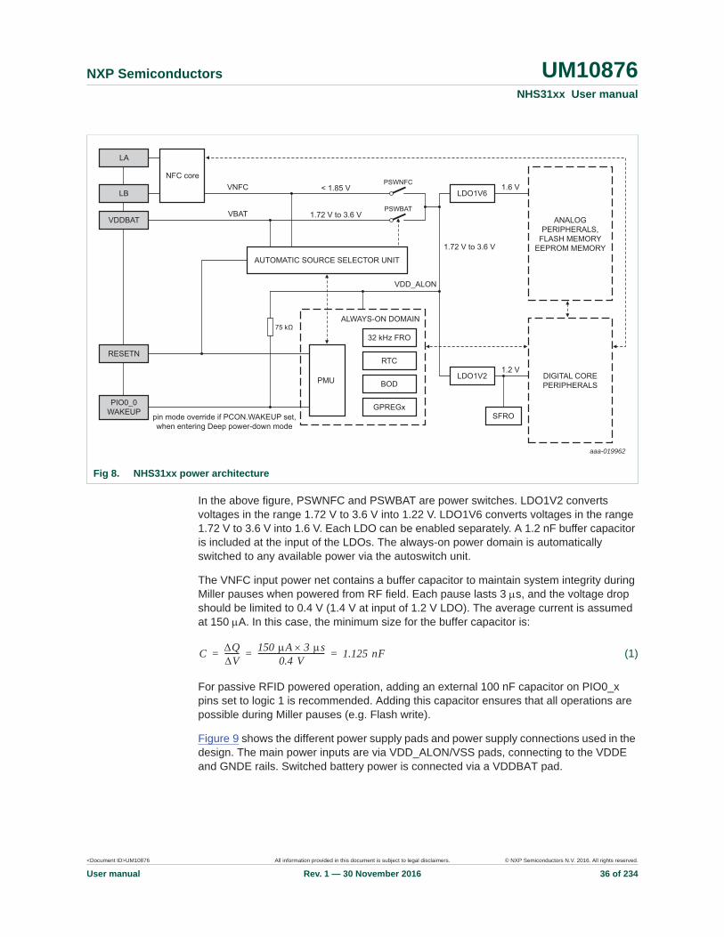
5.4 System power architectureThe NHS31xx platform accepts power from two different sources: from the external power supply pin VDDBAT (domain VBAT), or from the built-in NFC/RFID rectifier (domain VNFC).
VDD_ALON via the VDD_ALON pad powers the external ring (VDDE) of the IO pads, as shown in Figure 8. Note: the pad ring does not power the VDDBAT pin, it is thus not possible to power external devices connected to this pin. In Passive RF mode, external devices can be powered by connecting them to a PIO0_n (preferably a high-drive pin) set to output logic 1.
The PMU in the always-on domain then decides on the powering of the internal domains.
The power source decision is as follows:
• If voltage is detected on VBAT and not on VNFC, VBAT powers the internal domains• If voltage < 1.72 V is detected on VBAT, and higher voltage is detected on VNFC,
VNFC powers the internal domains• If voltage > 1.72 V is detected at both VBAT and VNFC, VBAT powers the internal
domains
<Document ID>UM10876 All information provided in this document is subject to legal disclaimers. © NXP Semiconductors N.V. 2016. All rights reserved.
User manual Rev. 1 — 30 November 2016 35 of 234
NXP Semiconductors UM10876NHS31xx User manual
• Switchover between sources is possible. For example, if initially both VBAT and VNFC are available, the system is powered from VBAT. If VBAT then becomes unavailable because it is switched off externally or the PSWBAT power switch is overridden, the internal domains are immediately powered from VNFC. Switchover is supported in both directions
• When on NFC power only (passive operation), connect a 100 nF external capacitor to a GPIO pad set as an output driven to logic 1
• The user can disable the automatic switching by setting bit PMULPM in the PCON register. Setting this bit disables the voltage comparator and forces the selection of the VDDBAT input.
When the system is in Deep Power-down mode, the power source selection is handled in the same way. The powering of the internal domains then depends on the wake-up conditions set by the user: Wake-up due to a 1-to-0 transition on the WAKEUP pin (if WAKEUP is enabled in the PIO0_0 register), an RTC timer event, or an NFC event.
When the WAKEUP function on PIO0_0 is enabled in the PCON register, and the DPEN is set, the NHS31xx overrides the user settings of the PIO0_0 pad before entering Deep power-down. The pad is set to wake-up and the pull-up is enabled.
The PSTAT register contains all information on the configuration of the power supplies. The system Power-On Reset reacts on VDD1V2.
The power architecture of the NHS31xx is shown in Figure 8. The (analog) IC power controller arbitrates between external battery power (VBAT) and RF power (VNFC) and controls the main power switches. The Power management unit controls the LDOs and the power flow to the different circuits block inside the NHS31xx, as well as the different sleep modes. It interacts with the RTC Timer (refer to section 4.16) and the ARM Cortex-M0+ core. The RTC timer resides partly in the always-on power domain, partly in the 1.2 V domain. It generates a power-on request signal toward the PMU.
<Document ID>UM10876 All information provided in this document is subject to legal disclaimers. © NXP Semiconductors N.V. 2016. All rights reserved.
User manual Rev. 1 — 30 November 2016 36 of 234
NXP Semiconductors UM10876NHS31xx User manual
In the above figure, PSWNFC and PSWBAT are power switches. LDO1V2 converts voltages in the range 1.72 V to 3.6 V into 1.22 V. LDO1V6 converts voltages in the range 1.72 V to 3.6 V into 1.6 V. Each LDO can be enabled separately. A 1.2 nF buffer capacitor is included at the input of the LDOs. The always-on power domain is automatically switched to any available power via the autoswitch unit.
The VNFC input power net contains a buffer capacitor to maintain system integrity during Miller pauses when powered from RF field. Each pause lasts 3 s, and the voltage drop should be limited to 0.4 V (1.4 V at input of 1.2 V LDO). The average current is assumed at 150 A. In this case, the minimum size for the buffer capacitor is:
(1)
For passive RFID powered operation, adding an external 100 nF capacitor on PIO0_x pins set to logic 1 is recommended. Adding this capacitor ensures that all operations are possible during Miller pauses (e.g. Flash write).
Figure 9 shows the different power supply pads and power supply connections used in the design. The main power inputs are via VDD_ALON/VSS pads, connecting to the VDDE and GNDE rails. Switched battery power is connected via a VDDBAT pad.
Fig 8. NHS31xx power architecture
aaa-019962
AUTOMATIC SOURCE SELECTOR UNIT
< 1.85 V
1.72 V to 3.6 V
1.72 V to 3.6 V
1.2 V
75 kΩ
PMU
32 kHz FRO
ALWAYS-ON DOMAIN
pin mode override if PCON.WAKEUP set,when entering Deep power-down mode
DIGITAL COREPERIPHERALS
VDD_ALON
PSWNFC
PSWBAT
VNFC
VBAT
RESETN
VDDBAT
LB
LA
PIO0_0WAKEUP
ANALOGPERIPHERALS,
FLASH MEMORYEEPROM MEMORY
NFC core
RTC
BODLDO1V2
SFRO
LDO1V6
GPREGx
1.6 V
C QV
-------- 150 A 3 s0.4 V
------------------------------------ 1.125 nF= = =

<Document ID>UM10876 All information provided in this document is subject to legal disclaimers. © NXP Semiconductors N.V. 2016. All rights reserved.
User manual Rev. 1 — 30 November 2016 37 of 234
NXP Semiconductors UM10876NHS31xx User manual
The PMU states and settings of the LDOs are summarized in Table 29, and the state transitions are shown in Figure 10.
[1] DPDN indicates whether the system is in Deep power-down.
[2] DSLP indicates that the system is in Deep-sleep.
[3] The value of VDD_RFID is X instead of logic 0 if the RFID interrupt is disabled in the PMU settings.
Fig 9. Power rails and power supply pad types.
Table 29. IC power statesState VDD_ALON DPDN[1] DSLP[2] LDO1 1.2 V LDO2 1.6 VNOPOWER no X X X X
ACTIVE yes 0 0 on on
DEEPPDN yes [3] 1 0 off off
DEEPSLEEP yes [3] 0 1 on off
Fig 10. PMU state transition diagram
aaa-019372
VDD_ALON
gnde
vdde
gnd
vdd
VSS
VDDBATvbat
vnfc
VDD1V2
VDD1V6
LDO 1V2
PSWBAT
PSWNFC
LDO 1V6vss
vdd1v2
vdd1v6
PMU
aaa-019373
BATTERY-OFF
ACTIVE
DEEPPOWER-DOWN
SLEEP ORDEEP-SLEEP

<Document ID>UM10876 All information provided in this document is subject to legal disclaimers. © NXP Semiconductors N.V. 2016. All rights reserved.
User manual Rev. 1 — 30 November 2016 38 of 234
NXP Semiconductors UM10876NHS31xx User manual
The RESETN signal also forces a ’request power-on’ when in Deep power-down or Deep-sleep to avoid deadlock situations. Table 30 and Table 31 summarize the events that can influence wake-up from Deep-sleep or Deep power-down (DEEPPDN or DEEPSLEEP to ACTIVE state transition).
The power-up sequence is shown in Figure 11. When external power is applied and the PSUBAT switch closed, the always-on part gets a power-on reset signal and the timer FRO starts running. The TFRO starts a small state machine in the PMU. In the first state, the LDO powering the digital domain is started. In the second state, the LDO powering the 1.6 V analog domain is started. In the last state, the system is considered ’on’. The transition from ’off’ to ’on’ takes approximately 92 s. In the VDD1V2 domain, enabling the LDO1 and SFRO triggers the system_por. The system can boot when the Flash memory is operational.
If there is no external power, but there is RF power, the same procedure is followed except that PSWNFC connects power to the LDOs.
The user cannot disable the TFRO as it is used by the PMU.
Table 30. State transition events for DEEPSLEEP to ACTIVEEvent DescriptionRESETN reset asserted
RTC event if the timer reaches pre-set value
Watchdog watchdog issues interrupt or reset
WAKEUP signal on WAKEUP pin or pins defined for exit out of Deep-sleep
RF field RF field is detected, potential NFC command input (if set in PMU)
Start logic interrupt one of the enabled start logic interrupts is asserted
Table 31. State transition events for DEEP POWER-DOWN to ACTIVEEvent DescriptionRESETN reset asserted
RTC event if the timer reaches pre-set value
WAKEUP signal on WAKEUP pin
RF field RF field is detected, potential NFC command input (if set in PMU)
Fig 11. NHS31xx power-up sequence
aaa-016479
VDD_ALON
start TFRO enable 1.2 V LDO
enable 1.6 V LDOfor analog domainand flash memory
POR always-ondomain
SFRO starts running
powerflash and
digitalpoweranalog
on
off
SFRO stable (64 μs)
system_por
<Document ID>UM10876 All information provided in this document is subject to legal disclaimers. © NXP Semiconductors N.V. 2016. All rights reserved.
User manual Rev. 1 — 30 November 2016 39 of 234
NXP Semiconductors UM10876NHS31xx User manual
5.5 Brown-out detectionThe NHS31xx monitors the voltage on VDD_ALON. If this voltage falls below the threshold level (1.8 V), the BOD asserts an interrupt.
The interrupt detection has a hysteresis of 75 mV.
5.6 Register DescriptionsAll PMU registers need a synchronized access. See Section 5.6.4.
5.6.1 Power control register (PCON)The power control register selects whether one of the ARM Cortex-M0+ controlled Power-down modes (Sleep mode or Deep-sleep mode) or the Deep power-down mode is entered. The register also provides the flags for Sleep or Deep-sleep modes and Deep power-down modes respectively. It also contains the overrides for the power source selection.
Table 32. Register overview: PMU (base address 0x4003 8000)Name Access Address
offsetDescription Reset value
PCON R/W 0x000 power control register 0x0000 0000
GPREG0 R/W 0x004 general-purpose register 0 0x0000 0000
GPREG1 R/W 0x008 general-purpose register 1 0x0000 0000
GPREG2 R/W 0x00C general-purpose register 2 0x0000 0000
GPREG3 R/W 0x010 general-purpose register 3 0x0000 0000
GPREG4 R/W 0x014 general-purpose register 4 0x0000 0000
PSTAT R 0x018 power management unit status register n/a
- - 0x01C (reserved) -
ACCSTAT R 0x020 access status register 0x0000 0001
LDO1V6 R/W 0x024 analog 1.6 V LDO trimming 0x0000 0004
TMRCLKCTRL R/W 0x02C timer clock control register 0x0060 0001
IMSC R/W 0x030 interrupt mask set and clear Register 0x0000 0000
RIS R 0x034 raw interrupt status register 0x0000 0000
MIS R 0x038 masked interrupt status register 0x0000 0000
ICR W 0x03C interrupt clear register n/a
Table 33. PCON register (address 0x4003 8000) bit descriptionBit Symbol Value Description Reset
value0 - - (reserved. Do not write 1 to this bit) 0
1 DPEN - Deep power-down mode enable 0
0 ARM WFI enters Sleep or Deep-sleep mode (clock to ARM Cortex-M0+ core turned off)
1 ARM WFI enters Deep-power down mode (ARM Cortex-M0+ core powered down)
7:2 - - (reserved. Do not write 1 to this bit) 0
<Document ID>UM10876 All information provided in this document is subject to legal disclaimers. © NXP Semiconductors N.V. 2016. All rights reserved.
User manual Rev. 1 — 30 November 2016 40 of 234
NXP Semiconductors UM10876NHS31xx User manual
[1] Setting the PMULPM bit disables the automatic switching. It is recommended only when on battery power and no switching to NFC is foreseen.
[2] Setting the WAKEUP bit enables the wake-up function of the PIO0_0 pad. Upon entering Deep power-down, the pad is automatically set to input with disabled receiver, and enabled pull-up resistor. If this bit is not set, it is not possible to exit Deep power-down via the PIO0_0 pin.
5.6.2 General-purpose registers 0 to 4 (GPREG0-4)
The general-purpose registers retain data through Deep power-down mode when power is still applied to the VDDBAT pin but the chip has entered Deep power-down mode. Only a cold boot when all external and RF power has been removed from the chip, or a hard reset (asserting the RESETN pin), resets the general-purpose registers.
8 SLEEPFLAG - Sleep mode flag 0
0 read: No Power-down mode enteredwrite: No effect
1 read: Sleep/Deep-sleep mode enteredwrite: write logic 1 to clear SLEEPFLAG
10:9 - - (reserved. Do not write 1 to these bits) 0
11 DPDFLAG - Deep power-down flag 0
0 read: No power-down mode enteredwrite: No effect
1 read: Deep power-down mode enteredwrite: Clear the deep power-down flag
12 - - (reserved. Do not write 1 to this bit) 0
13 PMULPM [1] - PMU ultra-low-power mode 0
0 power switches are in automatic mode
1 disable automatic switching (default to external power)
14 VBAT - Battery switch control 0
0 Automatic mode
1 force off (disconnect external battery)
15 BODEN - Brown-Out Detector enable 0
0 BOD disabled
1 BOD enabled
16 - - (reserved. Do not write 1 to this bit) 0
18:17 FORCEVBATFORCEVNFC
- force the power source selection 0
01 force to VBAT/external power
10 force to NFC power
11 autoswitching if PMULPM is 0
19 WAKEUP [2] - enable the WAKEUP function on pin PIO0_0 -
0 WAKEUP function not enabled
1 WAKEUP function assigned to PIO0_0. When selecting this option, PIO0_0 has a weak pull-up to VDD_ALON when in Deep power-down.
31:20 - - (reserved. Do not write 1 to this bit) -
Table 33. PCON register (address 0x4003 8000) bit description _continued
Bit Symbol Value Description Reset value

<Document ID>UM10876 All information provided in this document is subject to legal disclaimers. © NXP Semiconductors N.V. 2016. All rights reserved.
User manual Rev. 1 — 30 November 2016 41 of 234
NXP Semiconductors UM10876NHS31xx User manual
5.6.3 Power status register (PSTAT)The power status register indicates the power source and configuration of LDOs and power switches. Reading the PSTAT register clears the BOD and RFPOW interrupts.
[1] The BOD1V7 and RFPOW signals are real-time (immediate) values, and might differ from the corresponding interrupts
5.6.4 Access status register (ACCSTAT)The access status register indicates whether the PMU is able to accept data over the APB. The PMU runs at a different clock rate than the core system therefore bus synchronization is necessary. This mechanism is described below.
Write access
The write procedure is as follows:
Table 34. GPREG0 - GPREG3 registers (address 0x4003 8004 to 0x4003 8014) bit description
Bit Symbol Value Description Reset value
31:0 GPDATA - data retained during Deep power-down mode 0
Table 35. PSTAT register (address 0x4003 8018) bit descriptionBit Symbol Value Description Reset
value0 PSWNFC - status of NFC power selection switch 1 or 0
0 switch disabled (not conducting)
1 switch enabled (conducting)
1 PSWBAT - status of battery power selection switch 0 or 1
0 switch disabled (not conducting)
1 switch enabled (conducting)
2 - - (reserved) 0 or 1
4:3 DPDEXIT - reason for exit from Deep-Power Down. Only valid when the DPDFLAG in the PCON register is asserted (1)
0
00 POR or RESETN pin asserted
01 LDO enabled
10 RTC timer event
11 WAKEUP pin negative edge detected
5 BOD1V8[1] - BOD detected (VDD < 1.8 V) 0
0 VDD 1.8 V
1 VDD 1.8 V
6 - - (reserved)
7 RFPOW [1] - RF field detected 0
0 no field
1 RF field
31:7 - (reserved) -

<Document ID>UM10876 All information provided in this document is subject to legal disclaimers. © NXP Semiconductors N.V. 2016. All rights reserved.
User manual Rev. 1 — 30 November 2016 42 of 234
NXP Semiconductors UM10876NHS31xx User manual
• When the ARM writes to a PMU register:– The address/value pair is stored in the command-buffer – The direction flag is set to write– ACCSTAT goes to logic 0 indicating a command is pending. This transition
happens on an edge of the APB clock, which is faster than the TFRO clock. • When the TFRO clock edge comes, the address/value in the command-buffer is
written to the RTC block• On a next TFRO edge, the ACCSTAT goes to logic 1 to indicate that no command is
pending and a new one can be given
Read access
The read procedure is as follows:
• When a value is stored in the PMU register for the ARM to read;– Only the register address is stored in the command-buffer– The direction flag is set to read– ACCSTAT goes to logic 0 indicating a command is pending.
• When the TFRO clock edge arrives, the address in the buffer is used to read the actual RTC register. This register value is copied in the data part of the command-buffer
• On the next TFRO edge, the ACCSTAT goes to logic 1 to indicate that the command is completed
• The ARM should do another read from a PMU register. This read ensures that the actual register value is picked up from that data part of the command-buffer
• The command-buffer sees that the address of the second read is the same as the address part in the command-buffer. In this case, the result is not treated as a new read command (ACCSTAT stays logic 1)
• However, the address part of the command-buffer is now cleared, so that a third read (even when from the same PMU register) causes a new command
5.6.5 Timer clock control register (TMRCLKCTRL)The timer clock control register controls the 32 kHz oscillator and RTC clock source. Note: this register resides in the always-on power domain, hence its location in the PMU. The 32 kHz TFRO is always running when VDD_ALON is available.
Table 36. ACCSTAT register (address 0x4003 8020) bit descriptionBit Symbol Description Reset
value0 PMU_READY logic 0: PMU access not possible, logic 1: PMU access possible 1
31:1 - (reserved) -
Table 37. TMRCLKCTRL register (address 0x4003 802C) bit descriptionBit Symbol Value Description After boot0 TMREN - RTC clock source. 1
0 no clock
1 32 kHz FRO

<Document ID>UM10876 All information provided in this document is subject to legal disclaimers. © NXP Semiconductors N.V. 2016. All rights reserved.
User manual Rev. 1 — 30 November 2016 43 of 234
NXP Semiconductors UM10876NHS31xx User manual
5.6.6 PMU Interrupt mask set and clear register (IMSC)This register controls whether each of the two possible interrupt conditions in the PMU are enabled.
5.6.7 PMU Raw interrupt status register (RIS)This read-only register contains a logic 1 for each interrupt condition that is asserted, regardless of whether the interrupt is enabled in the IMSC register.
5.6.8 PMU Masked interrupt status register (MIS)This read-only register contains a logic 1 for each interrupt condition that is asserted and enabled in the IMSC registers.
5.6.9 PMU Interrupt clear register (ICR)Software can write one or more logic 1s to this write-only register, to clear the corresponding interrupt condition or conditions in the PMU. Note: the interrupt conditions can be disabled by clearing the corresponding bit in IMSC registers
15:1 - - (reserved) -
21:16 TMRCLKTRIM - timer FRO trim value (6-bit) device dependent
23:22 TMRCURRLVL - timer FRO current level selector bits device dependent
31:24 - - (reserved) -
Table 37. TMRCLKCTRL register (address 0x4003 802C) bit descriptionBit Symbol Value Description After boot
Table 38. IMSC register (address 0x4003 8030) bit descriptionBit Symbol Description Reset
value0 BODI software should set this bit to enable an interrupt when the BOD
is triggered0
1 RFPOWI software should set this bit to enable an interrupt when RF power is detected
0
31:2 - (reserved) 0
Table 39. RIS register (address 0x4003 8034) bit descriptionBit Symbol Description Reset
value0 BODRI raw BOD interrupt value 0
1 RFPOWRI raw RF power interrupt value 0
31:2 - (reserved) 0
Table 40. MIS register (address 0x4003 8038) bit descriptionBit Symbol Description Reset
value0 BODRI raw BOD interrupt value 0
1 RFPOWRI raw RF power interrupt value 0
31:2 - (reserved) 0

<Document ID>UM10876 All information provided in this document is subject to legal disclaimers. © NXP Semiconductors N.V. 2016. All rights reserved.
User manual Rev. 1 — 30 November 2016 44 of 234
NXP Semiconductors UM10876NHS31xx User manual
Table 41. ICR register (address 0x4003 803C) bit descriptionBit Symbol Description Reset
value0 BODC writing a logic 1 clears the BOD interrupt 0
1 RFPOWC writing a logic 1 clears the RF power interrupt 0
31:2 - (reserved) 0
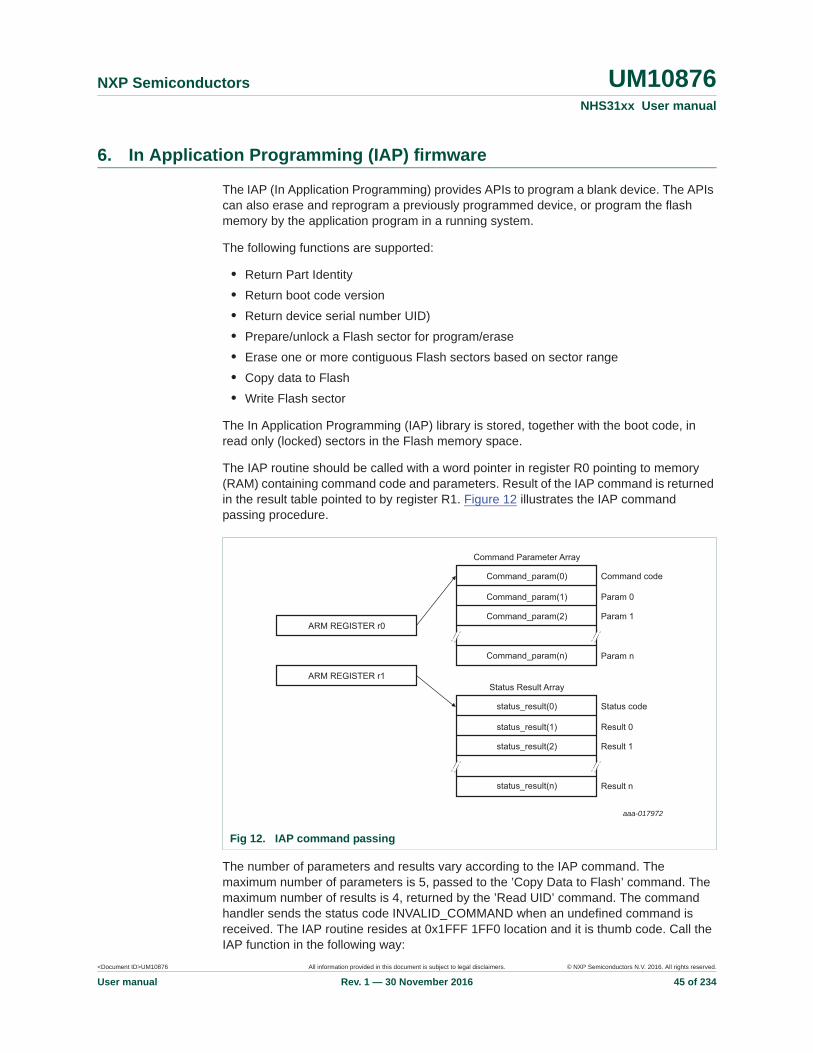
<Document ID>UM10876 All information provided in this document is subject to legal disclaimers. © NXP Semiconductors N.V. 2016. All rights reserved.
User manual Rev. 1 — 30 November 2016 45 of 234
NXP Semiconductors UM10876NHS31xx User manual
6. In Application Programming (IAP) firmware
The IAP (In Application Programming) provides APIs to program a blank device. The APIs can also erase and reprogram a previously programmed device, or program the flash memory by the application program in a running system.
The following functions are supported:
• Return Part Identity• Return boot code version• Return device serial number UID)• Prepare/unlock a Flash sector for program/erase• Erase one or more contiguous Flash sectors based on sector range• Copy data to Flash• Write Flash sector
The In Application Programming (IAP) library is stored, together with the boot code, in read only (locked) sectors in the Flash memory space.
The IAP routine should be called with a word pointer in register R0 pointing to memory (RAM) containing command code and parameters. Result of the IAP command is returned in the result table pointed to by register R1. Figure 12 illustrates the IAP command passing procedure.
The number of parameters and results vary according to the IAP command. The maximum number of parameters is 5, passed to the ’Copy Data to Flash’ command. The maximum number of results is 4, returned by the ’Read UID’ command. The command handler sends the status code INVALID_COMMAND when an undefined command is received. The IAP routine resides at 0x1FFF 1FF0 location and it is thumb code. Call the IAP function in the following way:
Fig 12. IAP command passing
aaa-017972
Command Parameter Array
Command_param(0) Command code
Param 0
Param 1
Param n
Command_param(1)
Command_param(2)ARM REGISTER r0
ARM REGISTER r1
Command_param(n)
Status Result Array
status_result(0) Status code
Result 0
Result 1
Result n
status_result(1)
status_result(2)
status_result(n)

<Document ID>UM10876 All information provided in this document is subject to legal disclaimers. © NXP Semiconductors N.V. 2016. All rights reserved.
User manual Rev. 1 — 30 November 2016 46 of 234
NXP Semiconductors UM10876NHS31xx User manual
Step 1: Define the IAP location entry point. Bit 0 of the IAP location is set to logic to indicate that it is a Thumb instruction at the destination address.
#define IAP_LOCATION 0x1fff 1ff1
Step 2: To pass IAP command table and result table to the IAP function, define data structure or pointers:
unsigned int command_param[5];unsigned int status_result[4];
or
unsigned int * command_param;unsigned int * status_result;command_param = (unsigned int *) 0x...status_result = (unsigned int *) 0x...
Step 3: Define function type pointer, which takes two parameters and returns void. Note the IAP returns the result with the base address of the table residing in R1.
typedef void (*IAP)(unsigned int [],unsigned int[]);IAP iap_entry;
Setting the function pointer:
iap_entry=(IAP) IAP_LOCATION;
Step 4: To call the IAP, use the following statement.
iap_entry (command_param,status_result);
The flash memory is not accessible during program/erase operations. IAP commands, which result in a flash write/erase operation, use 16 bytes of space in the top portion of the on-chip RAM for execution. This portion is initialized at boot, and if the user application executes IAP calls for flash programming, this area should be left untouched.
Many of the IAP commands access non-volatile memories, and may cause temporary power consumption increase.
6.1 IAP command list
Table 42. IAP command listIAP Command Command code Reference
hex decimalRead factory settings 28h 40d Section 6.1.1
Prepare sectors for write operation 32h 50d Section 6.1.2
Copy data to flash 33h 51d Section 6.1.3
Erase sectors 34h 52d Section 6.1.4
Blank check sectors 35h 53d Section 6.1.5
Read part identity 36h 54d Section 6.1.6
Read boot code version 37h 55d Section 6.1.7
<Document ID>UM10876 All information provided in this document is subject to legal disclaimers. © NXP Semiconductors N.V. 2016. All rights reserved.
User manual Rev. 1 — 30 November 2016 47 of 234
NXP Semiconductors UM10876NHS31xx User manual
After power-on reset, all flash sectors are protected. To erase or write to sectors or pages, the user first must issue the ’Prepare sectors for write operation’ command to unprotect the corresponding sectors.
For example, if the user wants to write data to sector 6 the following procedure should be followed:
1. Call the ’Prepare’ command (code: 50d) for sector 62. Call the ’Erase’ command (code: 52d) to erase sector 63. Call the ’Prepare’ command (code: 50d) again4. Call the ’Copy Data to Flash’ command (code: 51d) to write data to sector 6
Remark: During an erase or program operation, the flash is not accessible. Hence, if the Interrupt Vector Table is placed in Flash (default setup) the application should make sure that no interrupts are triggered. Accessing the table, if in flash, results in a hard fault.
6.1.1 Read factory settingsThis command reads the factory settings for calibration registers.
[1] Only applicable to devices that support temperature sensors
Compare 38h 56d Section 6.1.8
Read UID 3Ah 58d Section 6.1.9
Erase page 3Bh 59d Section 6.1.10
Table 42. IAP command listIAP Command Command code Reference
hex decimal
Table 43. IAP Read factory settings commandCommand Read factory settingsInput command code: 40 (decimal)
param0: The address of the targeted calibration register. Refer to Table 44 for supported registers
Status code CMD_SUCCESS | PARAMETER_ERROR
Result result0: The factory value when the status code is CMD_SUCCESS.PARAMETER_ERROR is returned when param0 is not one of the supported calibration registers
Description this command provides users with the capability to read the factory value for the calibration registers
Table 44. Supported registers for factory setting readParameter 0 Description0x4006 0010 [1] TSENSP1: Temperature sensor setup register 1
0x4006 0014 [1] TSENSP2: Temperature sensor setup register 2
0x4006 0018 [1] TSENSP3: Temperature sensor setup register 3
0x4005 4008 RTCCAL: RTC timer calibration register

<Document ID>UM10876 All information provided in this document is subject to legal disclaimers. © NXP Semiconductors N.V. 2016. All rights reserved.
User manual Rev. 1 — 30 November 2016 48 of 234
NXP Semiconductors UM10876NHS31xx User manual
6.1.2 Prepare sectors for write operationThis command makes the sector or sectors unprotected.
6.1.3 Copy data to flashThis command copies the data from the RAM buffer / EEPROM to the specified flash area to be written.
[1] These devices are not able to select external clocks.
Table 45. IAP Prepare sectors for write operation commandCommand Prepare sector for write operationInput command code: 50 (decimal)
param0: Start Sector Numberparam1: End Sector Number (should be greater than or equal to start sector number)
Status code CMD_SUCCESS | INVALID_SECTOR
Result none
Description this command must be executed before executing ’Copy Data to flash’ or ’Erase Sectors’ command. Successful execution of the ’Copy Data to flash’ or ’Erase Sectors’ command causes relevant sectors to be protected again. This command cannot be used to prepare the boot sector. To prepare a single sector, use the same ’Start’ and ’End’ sector numbers
Table 46. IAP Copy data to flash commandCommand Copy data to flashInput command code: 51 (decimal)
param0 (DST): Destination flash write address. This address should be a 64 byte boundaryparam1 (SRC): Source read address (RAM / EEPROM). This address should be a word boundaryparam2: Number of bytes to be written. Must be a multiple of 64param3: System clock frequency (CCLK) in kHz. This parameter is ignored[1]
Status code CMD_SUCCESS |SRC_ADDR_ERROR (Address not a word boundary) |DST_ADDR_ERROR (Address not on correct boundary) |VDST_ADDR_NOT_VALID |VSRC_ADDR_NOT_VALID |COUNT_ERROR (Byte count is not a multiple of the page size) |SECTOR_NOT_PREPARED_FOR_WRITE_OPERATION
Result none
Description this command is used to program the flash memory. The affected sectors should be prepared first by calling ’Prepare Sector for Write Operation’ command. The flash area to be written should be blank (or cleared) before the operation is called. The affected sectors are automatically protected again once the copy command is successfully executed. This command cannot be used to write to the boot sector
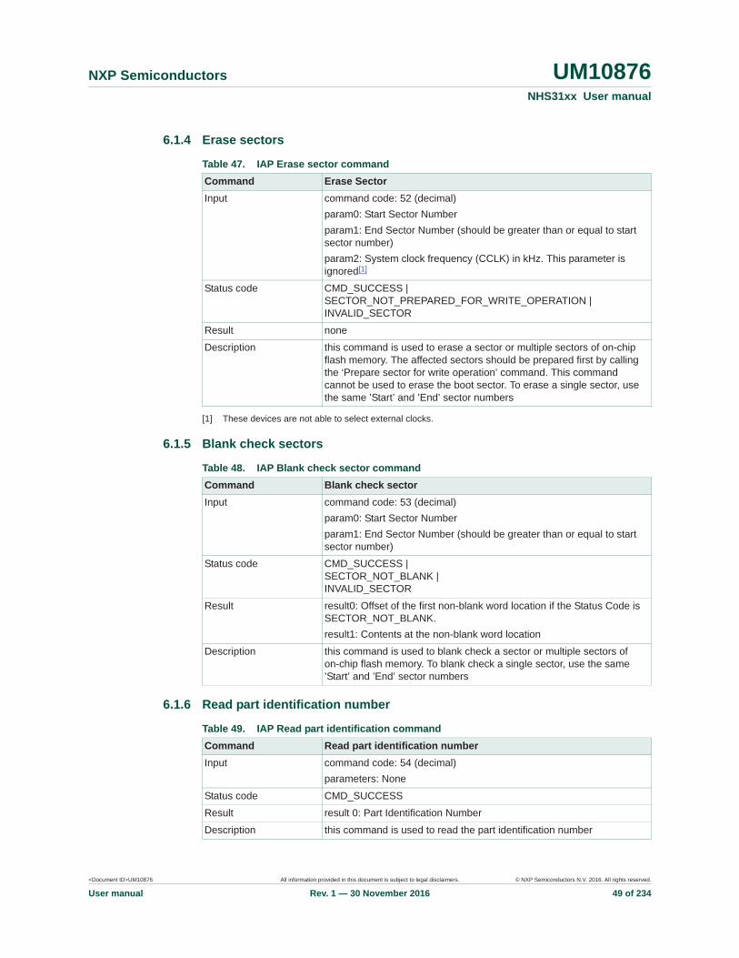
<Document ID>UM10876 All information provided in this document is subject to legal disclaimers. © NXP Semiconductors N.V. 2016. All rights reserved.
User manual Rev. 1 — 30 November 2016 49 of 234
NXP Semiconductors UM10876NHS31xx User manual
6.1.4 Erase sectors
[1] These devices are not able to select external clocks.
6.1.5 Blank check sectors
6.1.6 Read part identification number
Table 47. IAP Erase sector commandCommand Erase SectorInput command code: 52 (decimal)
param0: Start Sector Numberparam1: End Sector Number (should be greater than or equal to start sector number)param2: System clock frequency (CCLK) in kHz. This parameter is ignored[1]
Status code CMD_SUCCESS |SECTOR_NOT_PREPARED_FOR_WRITE_OPERATION |INVALID_SECTOR
Result none
Description this command is used to erase a sector or multiple sectors of on-chip flash memory. The affected sectors should be prepared first by calling the ‘Prepare sector for write operation’ command. This command cannot be used to erase the boot sector. To erase a single sector, use the same ’Start’ and ’End’ sector numbers
Table 48. IAP Blank check sector commandCommand Blank check sectorInput command code: 53 (decimal)
param0: Start Sector Numberparam1: End Sector Number (should be greater than or equal to start sector number)
Status code CMD_SUCCESS |SECTOR_NOT_BLANK |INVALID_SECTOR
Result result0: Offset of the first non-blank word location if the Status Code is SECTOR_NOT_BLANK.result1: Contents at the non-blank word location
Description this command is used to blank check a sector or multiple sectors of on-chip flash memory. To blank check a single sector, use the same ’Start’ and ’End’ sector numbers
Table 49. IAP Read part identification commandCommand Read part identification numberInput command code: 54 (decimal)
parameters: None
Status code CMD_SUCCESS
Result result 0: Part Identification Number
Description this command is used to read the part identification number

<Document ID>UM10876 All information provided in this document is subject to legal disclaimers. © NXP Semiconductors N.V. 2016. All rights reserved.
User manual Rev. 1 — 30 November 2016 50 of 234
NXP Semiconductors UM10876NHS31xx User manual
6.1.7 Read boot code version number
[1] Ignore the data contained in byte 2 and byte 3 in Result 0, which is for internal debugging purposes only.
6.1.8 Compare
6.1.9 Read UID
Table 50. IAP Read boot code version number commandCommand Read boot code version numberInput command code: 55 (decimal)
parameters: None
Status code CMD_SUCCESS
Result[1] result 0: 2 bytes of boot code version number. Read as <byte 1 (major)><byte 0 (minor)>
Description this command is used to read the boot code version number
Table 51. IAP Compare commandCommand CompareInput command code: 56 (decimal)
param0 (DST): Starting flash, RAM or EEPROM address of data bytes to be compared. This address should be a word boundaryparam1 (SRC): Starting flash, RAM or EEPROM address of data bytes to be compared. This address should be a word boundaryparam2: Number of bytes to be compared, and should be a multiple of 4
Status code CMD_SUCCESS |COMPARE_ERROR |COUNT_ERROR (Byte count is not a multiple of 4) |ADDR_ERROR
Result result0: If the Status Code is COMPARE_ERROR, the first mismatch is offset
Table 52. IAP Read Unique Identification number commandCommand Read UIDInput command code: 58 (decimal)
parameters: None
Status code CMD_SUCCESS
Result result 0: The first 32-bit wordresult 1: The second 32-bit wordresult 2: The third 32-bit wordresult 3: The fourth 32-bit word
Description this command is used to read the unique ID

<Document ID>UM10876 All information provided in this document is subject to legal disclaimers. © NXP Semiconductors N.V. 2016. All rights reserved.
User manual Rev. 1 — 30 November 2016 51 of 234
NXP Semiconductors UM10876NHS31xx User manual
6.1.10 Erase page
[1] These devices are unable to select external clocks.
6.2 IAP Status Codes
Table 53. IAP Erase page commandCommand Erase PageInput command code: 59 (decimal)
param 0: Start page numberparam 1: End page number (should be greater than or equal to start page)param 2: System clock frequency (CCLK) in kHz. This parameter is ignored[1]
Status code CMD_SUCCESS |SECTOR_NOT_PREPARED_FOR_WRITE_OPERATION |INVALID_SECTOR
Result none
Description this command is used to erase a page or multiple pages of on-chip flash memory. The affected sectors should be prepared first by calling ’Prepare Sector for Write Operation’ command. To erase a single page, use the same ’start’ and ’end’ page number
Table 54. IAP Status CodesStatus code
Mnemonic Description
0 CMD_SUCCESS command is executed successfully
1 INVALID_COMMAND invalid command
2 SRC_ADDR_ERROR source address is not on a word boundary
3 DST_ADDR_ERROR destination address is not on a correct boundary
4 SRC_ADDR_NOT_MAPPED source address is not mapped in the memory map. Count value is considered where applicable
5 DST_ADDR_NOT_MAPPED destination address is not mapped in the memory map. Count value is considered where applicable
6 COUNT_ERROR byte count is not a permitted value
7 INVALID_SECTOR sector number is invalid
8 SECTOR_NOT_BLANK sector is not blank
9 SECTOR_NOT_PREPARED_FOR_WRITE_OPERATION
command to prepare sector for write operation was not executed
10 COMPARE_ERROR source and destination data are not the same
11 - this error code is not used
12 PARAMETER_ERROR invalid parameter or Insufficient number of parameters
13 ADDR_ERROR address is not on a word boundary

<Document ID>UM10876 All information provided in this document is subject to legal disclaimers. © NXP Semiconductors N.V. 2016. All rights reserved.
User manual Rev. 1 — 30 November 2016 52 of 234
NXP Semiconductors UM10876NHS31xx User manual
7. Temperature sensor
7.1 About this chapterThis chapter describes the use of the temperature sensing feature of the NHS31xx family of sensor node ICs.
7.2 IntroductionThe temperature sensor is integrated into the chip and can accurately measure temperatures over a wide range.
7.3 FeaturesThe temperature sensor block measures the temperature of the die and outputs a calibrated value in Kelvin. It has a 0.3 °C absolute temperature accuracy between 0 °C and 40 °C, and 0.5 °C between 40 C to +85 C.
7.4 General descriptionRegister base address of the temperature sensor block: 0x4006 0000.
The temperature is measured using a high-precision zoom-ADC.
7.5 CalibrationThe temperature sensor calibration values are determined during manufacturing. For increased accuracy, the user can provide custom parameters A, B, and alpha. For calibration, the raw value X is needed, and high accuracy measurement is recommended. Internally, the following equation is used to obtain the calibrated temperature output:
(2)
The calibration values A, B, and alpha for the default resolution settings are determined during the calibration phase of the manufacturing process and stored in EEPROM.
For detailed information on calibrating the temperature sensor see the NHS3 Temperature sensor calibration application note, Ref. 5.
7.6 Register descriptionsThe register addresses for the temperature sensor are listed in Table 56.
Table 55. Conversion time for different resolution of TSENSResolution (bit) Resolution ( C) Conversion time (ms)7 ± 0.8 4
8 ± 0.4 7
9 ± 0.2 14
10 ± 0.1 26
11 ± 0.05 50
12 ± 0.025 100
T A X+------------- B+=

<Document ID>UM10876 All information provided in this document is subject to legal disclaimers. © NXP Semiconductors N.V. 2016. All rights reserved.
User manual Rev. 1 — 30 November 2016 53 of 234
NXP Semiconductors UM10876NHS31xx User manual
[1] Reset Value reflects the data stored in used bits only. It is not valid for the content of reserved bits.
7.6.1 Temperature sensor Control register (CR)
7.6.2 Temperature sensor Data register (DR)The DR register holds the current temperature data in either raw or calibrated format. Reading the DR register clears the temperature sensor interrupts.
7.6.3 Temperature sensor Status register (SR)
The SR register holds the status of the temperature sensor.
Table 56. Register overview for temperature sensor (base address 0x4006 0000)Name Access Address
offsetDescription After boot Reset value
[1]
CR R/W 0x0000 control register 0
DR R 0x0004 data register. Contains result of conversion 0
SR R 0x0008 status register 0x0000 0000
SP0 R/W 0x000C setup register 0: set ADC and operation modes 0x0000 000F
SP1 R/W 0x0010 setup register 1: Calibration value ‘A’ 0
SP2 R/W 0x0014 setup register 2: Calibration value ‘B’ 0
SP3 R/W 0x0018 setup register 3: Calibration value ’alpha’ 0
TLO R/W 0x001C low temperature threshold register 0x0000 8000
THI R/W 0x0020 high temperature threshold register 0x0000 7FFF
IMSC R/W 0x0024 interrupt Mask Set and Clear Register 0
RIS R 0x0028 raw Interrupt Status Register 0
MIS R 0x002C masked Interrupt Status Register 0
ICR W 0x0030 interrupt Clear Register n/a
Table 57. CR register (address 0x4006 0000) bit descriptionBit Symbol Description Reset value Access0 START sensor start bit. The temperature sensor clears this bit at the end of the
measurement0 R/W
31:1 - (reserved) - -
Table 58. DR register (address 0x4006 0004) bit descriptionBit Symbol Description Reset value Access15:0 TDATA result of last conversion. Format depending on the TOUTMODE bit of
the SP0 register. Raw format is unsigned fixed point (5.11); calibrated format is signed fixed point (10.6) 2-complement
0x0000 R
31:16 - (reserved) - -
Table 59. SR register (address 0x4006 0008) bit descriptionBit Symbol Description Reset value Access0 TRANLOC coarse range. Logic 1: out of range (too low) 0 R
1 TRANHIC coarse range. Logic 1: out of range (too high) 0 R
2 TRANLOF fine range. Logic 1: out of range (too low) 0 R
3 TRANHIF fine range. Logic 1: out of range (too large) 0 R
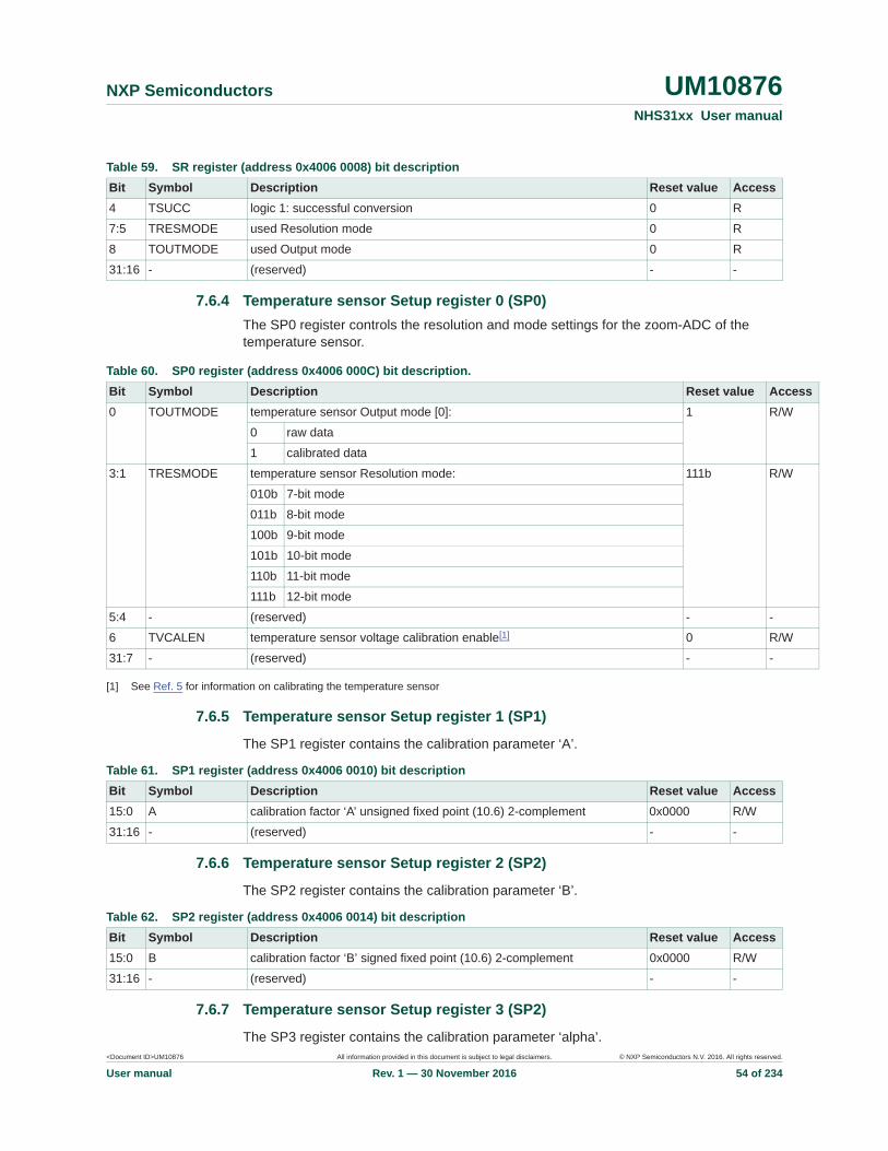
<Document ID>UM10876 All information provided in this document is subject to legal disclaimers. © NXP Semiconductors N.V. 2016. All rights reserved.
User manual Rev. 1 — 30 November 2016 54 of 234
NXP Semiconductors UM10876NHS31xx User manual
7.6.4 Temperature sensor Setup register 0 (SP0)The SP0 register controls the resolution and mode settings for the zoom-ADC of the temperature sensor.
[1] See Ref. 5 for information on calibrating the temperature sensor
7.6.5 Temperature sensor Setup register 1 (SP1)
The SP1 register contains the calibration parameter ‘A’.
7.6.6 Temperature sensor Setup register 2 (SP2)
The SP2 register contains the calibration parameter ‘B’.
7.6.7 Temperature sensor Setup register 3 (SP2)
The SP3 register contains the calibration parameter ‘alpha’.
4 TSUCC logic 1: successful conversion 0 R
7:5 TRESMODE used Resolution mode 0 R
8 TOUTMODE used Output mode 0 R
31:16 - (reserved) - -
Table 59. SR register (address 0x4006 0008) bit descriptionBit Symbol Description Reset value Access
Table 60. SP0 register (address 0x4006 000C) bit description.Bit Symbol Description Reset value Access0 TOUTMODE temperature sensor Output mode [0]: 1 R/W
0 raw data
1 calibrated data
3:1 TRESMODE temperature sensor Resolution mode: 111b R/W
010b 7-bit mode
011b 8-bit mode
100b 9-bit mode
101b 10-bit mode
110b 11-bit mode
111b 12-bit mode
5:4 - (reserved) - -
6 TVCALEN temperature sensor voltage calibration enable[1] 0 R/W
31:7 - (reserved) - -
Table 61. SP1 register (address 0x4006 0010) bit descriptionBit Symbol Description Reset value Access15:0 A calibration factor ‘A’ unsigned fixed point (10.6) 2-complement 0x0000 R/W
31:16 - (reserved) - -
Table 62. SP2 register (address 0x4006 0014) bit descriptionBit Symbol Description Reset value Access15:0 B calibration factor ‘B’ signed fixed point (10.6) 2-complement 0x0000 R/W
31:16 - (reserved) - -

<Document ID>UM10876 All information provided in this document is subject to legal disclaimers. © NXP Semiconductors N.V. 2016. All rights reserved.
User manual Rev. 1 — 30 November 2016 55 of 234
NXP Semiconductors UM10876NHS31xx User manual
7.6.8 Temperature sensor low-temperature threshold register (TLO)The TLO register contains the low-temperature threshold value, which is compared to the measured (calibrated) temperature. If the measured temperature is lower than the value in TLO and the corresponding bit in the IMSC register is set, then an interrupt is generated.
7.6.9 Temperature sensor high-temperature threshold register (THI)
The THI register contains the high-temperature threshold value, which is compared to the measured (calibrated) temperature. If the measured temperature is higher than the value in THI and the corresponding bit in the IMSC register is set, then an interrupt is generated.
7.6.10 Temperature sensor Interrupt Mask Set/Clear Register (IMSC)
This register controls which interrupts are enabled.
7.6.11 Temperature sensor Raw Interrupt Status Register (RIS)
This read-only register contains a logic 1 for each interrupt condition that is asserted, regardless of whether the interrupt is enabled in the IMSC register.
Table 63. SP3 register (address 0x4006 0018) bit descriptionBit Symbol Description Reset value Access15:0 ALPHA calibration factor ‘alpha’ unsigned fixed point (6.10) 2-complement 0x0000 R/W
31:16 - (reserved) - -
Table 64. TLO register (address 0x4006 001C) bit descriptionBit Symbol Description Reset value Access15:0 TLO low-temperature threshold value in signed fixed point (10.6)
2-complement0x8000 R/W
31:16 - (reserved) - -
Table 65. THI register (address 0x4006 0020) bit descriptionBit Symbol Description Reset value Access15:0 THI high-temperature threshold value in signed fixed point (10.6)
2-complement0x7FFF R/W
31:16 - (reserved) - -
Table 66. IMSC register (address 0x4006 0024) bit descriptionBit Symbol Description Reset value Access0 RDYI software should set this bit to enable interrupt when a temperature
conversion is ready on DR0 R/W
1 TLOE software should set this bit to enable interrupt when a temperature conversion is lower than the value stored in TLO
0 R/W
2 THIE software should set this bit to enable interrupt when a temperature conversion is higher than the value stored in THI
0 R/W
31:3 - (reserved) - -

<Document ID>UM10876 All information provided in this document is subject to legal disclaimers. © NXP Semiconductors N.V. 2016. All rights reserved.
User manual Rev. 1 — 30 November 2016 56 of 234
NXP Semiconductors UM10876NHS31xx User manual
7.6.12 Temperature sensor Register Masked Interrupt Status Register (MIS)
This read-only register contains a logic 1 for each interrupt condition that is asserted and enabled in the IMSC registers. When a temperature sensor interrupt occurs, the interrupt service routine should read this register to determine the cause or causes of the interrupt.
7.6.13 Temperature sensor Register Interrupt Clear Register (ICR)
Software can write one or more one(s) to this write-only register, to clear the corresponding interrupt condition or conditions in the temperature sensor controller. Note:the interrupt conditions can be cleared by reading the DR register or disabled by clearing the corresponding bit in IMSC registers.
Table 67. RIS register (address 0x4006 0028) bit descriptionBit Symbol Description Reset value Access0 RDYI this bit is logic 1 when a temperature conversion has finished 0 R
1 LOI software should set this bit to enable interrupt when a temperature conversion is below the value stored in TLO
0 R
2 HII this bit is logic 1 when a temperature conversion has finished and the value exceeds the THI threshold value
0 R
31:3 - (reserved) - -
Table 68. MIS register (address 0x4006 002C) bit descriptionBit Symbol Description Reset value Access0 RDYI this bit is logic 1 when a temperature conversion has finished and this
interrupt is enabled0 R
1 LOI this bit is logic 1 when a temperature conversion has finished, if the value is below the LOI threshold value, and this interrupt is enabled
0 R
2 HII this bit is logic 1 when a temperature conversion has finished, if the value exceeds the THI threshold value, and this interrupt is enabled
0 R
31:3 - (reserved) - -
Table 69. ICR register (address 0x4006 0030) bit descriptionBit Symbol Description Reset value Access0 RDYC writing a logic 1 clears the temperature sensor conversion ready
interrupt0 W
1 TLOC writing a logic 1 clears the temperature sensor low threshold interrupt 0 W
2 THIC writing a logic 1 clears the temperature sensor high threshold interrupt 0 W
31:3 - (reserved) - -

<Document ID>UM10876 All information provided in this document is subject to legal disclaimers. © NXP Semiconductors N.V. 2016. All rights reserved.
User manual Rev. 1 — 30 November 2016 57 of 234
NXP Semiconductors UM10876NHS31xx User manual
8. Current-to-Digital converter (I2D)
8.1 About this chapterThis chapter describes the setup and use of the Current-to-Digital converter
8.2 IntroductionOne of the available components of the NHS31xx family is a Current-to-Digital converter. This Current-to-Digital converter is based on a 16-bit I/F converter with selectable integration time.
Fig 13. Current-to-Digital block diagram
aaa-016411
APB
I2D APD SLAVE(0x4006 4000) CONTROL CURRENT
SCALER
to NVICinterrupt 24 PDRUNCFG[4] I2DMUX
I/FCONVERTER
COUNTER
POWER GATE
...

<Document ID>UM10876 All information provided in this document is subject to legal disclaimers. © NXP Semiconductors N.V. 2016. All rights reserved.
User manual Rev. 1 — 30 November 2016 58 of 234
NXP Semiconductors UM10876NHS31xx User manual
8.3 Input multiplexerThe input to the Current-to-Digital converter is connected to the analog buses and on-chip transducers via an analog multiplexer. Table 70 shows the inputs of the multiplexer.
Table 70. Connections to the Current-to-Digital analog input multiplexerAMUX input Source Description0 ana_extbus0 (external) pin ANA0_0
1 ana_extbus1 (external) pin ANA0_1
2 ana_extbus2 (external) pin ANA0_2
3 ana_extbus3 (external) pin ANA0_3
4 ana_extbus4 (external) pin ANA0_4
5 ana_extbus5 (external) pin ANA0_5

<Document ID>UM10876 All information provided in this document is subject to legal disclaimers. © NXP Semiconductors N.V. 2016. All rights reserved.
User manual Rev. 1 — 30 November 2016 59 of 234
NXP Semiconductors UM10876NHS31xx User manual
8.4 Register descriptionsThe register addresses for the Current-to-Digital converter are listed in Table 71. The register base address is 0x4006 8000.
The reset values reflect the data stored in used bits only, it does not include the content of reserved bits.
[1] Reset Value reflects the data stored in used bits only. It does not include content of reserved bits.
8.4.1 Current-to-Digital control register (CR)The Current-to-Digital converter control register sets the operation mode and start/stops the conversions.
8.4.2 Current-to-Digital data register (DR)The DR register holds a value proportional to the measured current as determined by the Current-to-Digital converter at the given input scaling. Reading the DR register clears the Current-to-Digital interrupts.
Table 71. Register overview: Current-to-Digital converter (base address 0x4006 8000)Name Access Address
offsetDescription Reset value
[1]
CR R/W 0x000 control register 0x0000 0000
DR R 0x004 data register. Contains result of conversion 0x0000 0000
SR R 0x008 status register 0x0000 0000
SP0 R/W 0x00C setup register 0: set ADC mode settings 0x0000 0043
SP1 R/W 0x010 setup register 1: integration time settings 0x0000 0000
SP2 R/W 0x014 setup register 2: integration time calibration 0x0000 0009
SP3 R/W 0x018 setup register 3: input gain settings 0x0000 0000
MUXA R/W 0x01C input multiplexer settings 0x0000 0000
TLO R/W 0x020 low value threshold register 0x0000 0000
THI R/W 0x024 high value threshold register 0x0000 FFFF
IMSC R/W 0x028 interrupt Mask Set and Clear Register 0x0000 0000
RIS R 0x02C raw Interrupt Status Register 0x0000 0000
MIS R 0x030 masked Interrupt Status Register 0x0000 0000
ICR W 0x034 interrupt Clear Register n/a
Table 72. CR register (address 0x4006 8000) bit descriptionBit Symbol Description Reset value Access0 START start bit. I2D clears this bit at the end of the measurement. 0 R/W
1 STOP stop bit. This bit stops the converter after the ongoing conversion in Continuous mode. There is no effect in single-shot mode
0 W
2 MODE Conversion mode: (0) single-shot, (1) continuous 0 R/W
31:3 - (reserved) 0 -

<Document ID>UM10876 All information provided in this document is subject to legal disclaimers. © NXP Semiconductors N.V. 2016. All rights reserved.
User manual Rev. 1 — 30 November 2016 60 of 234
NXP Semiconductors UM10876NHS31xx User manual
8.4.3 Current-to-Digital status register (SR)The SR register holds the status of the Current-to-Digital converter.
[1] Range too low indicates that the converted digital value is too high for the configured range. The 16-bit DATA value in the DR register is inaccurate.
[2] Range too high indicates that the converted digital value is too low for the configured range. The 16-bit DATA value in the DR register is inaccurate.
8.4.4 Current-to-Digital setup register 0 (SP0)The SP0 register controls the resolution and mode settings for the ADC of the Current-to-Digital converter.
Table 73. DR register (address 0x4006 8004) bit descriptionBit Symbol Description Reset value Access15:0 DATA result of last conversion, unsigned 16-bit integer 0 R
16 OFW (0) input in range, (1) overflow 0 R
31:17 - (reserved) 0 -
Table 74. SR register (address 0x4006 8008) bit descriptionBit Symbol Description Reset value Access0 OFW input out of range (overflow)[1] 0 R
1 UFW input out of range (underflow)[2] 0 R
31:2 - (reserved) 0 -
Table 75. SP0 register (address 0x4006 800C) bit descriptionBit Symbol Value Description Reset value Access2:0 INT integration time setting 0 R/W
000b (reserved)
001b 16 ms
010b 20 ms
011b 100 ms
100b 200 ms
101b 400 ms
110b (reserved)
111b custom integration time as defined by the SP1 register
5:3 - - (reserved) 0 -
6 GAIN0 - ADC internal gain setting 1 R/W
0 high gain
1 low gain
7 - - (reserved) 0 R/W
8 SELIOFF - enable offset current 0 R/W
9 IOFF0 - select offset current 0 0 R/W
10 IOFF1 - select offset current 1 0 R/W
31:11 - - (reserved) 0 -

<Document ID>UM10876 All information provided in this document is subject to legal disclaimers. © NXP Semiconductors N.V. 2016. All rights reserved.
User manual Rev. 1 — 30 November 2016 61 of 234
NXP Semiconductors UM10876NHS31xx User manual
8.4.5 Current-to-Digital setup register 1 (SP1)The SP1 register contains the custom integration time.
8.4.6 Current-to-Digital setup register 2 (SP2)The SP2 register contains calibration setting for the integration time (system clock to time calibration factor). When a custom integration time is selected in register SP0, this register has to be reset to 999 (decimal).
8.4.7 Current-to-Digital Setup Register 3 (SP3)The SP3 register contains the settings of the input current scaler.
[1] Not all combinations of IGAIN and GAIN0 are possible
8.4.8 Current-to-Digital input multiplexer (MUX)The MUX register contains the settings for the multiplexer of the Current-to-Digital converter.
Table 76. SP1 register (address 0x4006 8010) bit descriptionBit Symbol Description Reset value Access15:0 CINT custom integration time in ms 0 R/W
31:16 - (reserved) 0 -
Table 77. SP2 register (address 0x4006 8014) bit descriptionBit Symbol Description Reset value Access13:0 CAL integration time calibration to clock clock pulse to count 1 ms 9h R/W
31:14 - (reserved) 0 -
Table 78. SP3 register (address 0x4006 8018) bit descriptionBit Symbol Value Description Reset value Access0 GAIN_EN - input gain amplifier enable / bypass 1 R/W
0 gain amplifier bypassed
1 gain amplifier enabled
3:1 IGAIN [1] input gain / attenuation settings 0 R/W
000b no gain (analog input 1:1 output to I/F)
001b multiply input current by 2 (1:2)
010b multiply input current by 10 (1:10)
011b divide input current by 2 (2:1)
100b divide input current by 10 (10:1)
101b divide input current by 100 (100:1)
110b (reserved)
111b (reserved)
31:4 (reserved) 0 -

<Document ID>UM10876 All information provided in this document is subject to legal disclaimers. © NXP Semiconductors N.V. 2016. All rights reserved.
User manual Rev. 1 — 30 November 2016 62 of 234
NXP Semiconductors UM10876NHS31xx User manual
8.4.9 Current-to-Digital low-value threshold register (TLO)The TLO register contains the low threshold value. If the measured bit value is lower than this threshold value, and if corresponding bit in the IMSC register is set, then an interrupt is generated.
8.4.10 Current-to-Digital high-value threshold register (THI)The THI register contains the high threshold value. If the measured bit value is higher than this threshold value, and if corresponding bit in the IMSC register is set, then an interrupt is generated.
8.4.11 Current-to-Digital interrupt mask Set/Clear register (IMSC)This register controls whether each of the three possible interrupt conditions in the Current-to-Digital converter are enabled.
Table 79. MUX register (address 0x4006 801C) bit descriptionBit Symbol Description Reset value Access5:0 MUX each bit represents an input of the switching matrix. Logic 1: connected
to input, logic 0: disconnected0 R/W
31:6 - (reserved) 0 -
Table 80. TLO register (address 0x4006 4020) bit descriptionBit Symbol Description Reset value Access15:0 TLO low threshold value 0 R/W
31:16 - (reserved) 0 -
Table 81. THI register (address 0x4006 4024) bit descriptionBit Symbol Description Reset value Access15:0 THI high threshold value. 0xFFFF R/W
31:16 - (reserved) 0 -
Table 82. IMSC register (address 0x4006 8028) bit descriptionBit Symbol Description Reset value Access0 RDYI software should set this bit to enable interrupt when a conversion value
is ready in DR0 R/W
1 LO software should set this bit to enable interrupt when the value of the conversion is lower than the value stored in TLO
0 R/W
2 HI software should set this bit to enable interrupt when the conversion is higher than the value stored in THI
0 R/W
31:3 - (reserved) 0 -
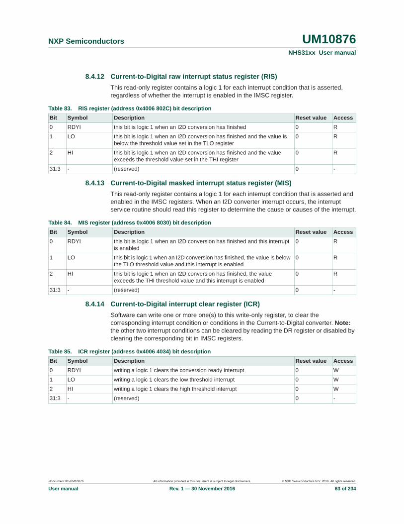
<Document ID>UM10876 All information provided in this document is subject to legal disclaimers. © NXP Semiconductors N.V. 2016. All rights reserved.
User manual Rev. 1 — 30 November 2016 63 of 234
NXP Semiconductors UM10876NHS31xx User manual
8.4.12 Current-to-Digital raw interrupt status register (RIS)This read-only register contains a logic 1 for each interrupt condition that is asserted, regardless of whether the interrupt is enabled in the IMSC register.
8.4.13 Current-to-Digital masked interrupt status register (MIS)This read-only register contains a logic 1 for each interrupt condition that is asserted and enabled in the IMSC registers. When an I2D converter interrupt occurs, the interrupt service routine should read this register to determine the cause or causes of the interrupt.
8.4.14 Current-to-Digital interrupt clear register (ICR)Software can write one or more one(s) to this write-only register, to clear the corresponding interrupt condition or conditions in the Current-to-Digital converter. Note:the other two interrupt conditions can be cleared by reading the DR register or disabled by clearing the corresponding bit in IMSC registers.
Table 83. RIS register (address 0x4006 802C) bit descriptionBit Symbol Description Reset value Access0 RDYI this bit is logic 1 when an I2D conversion has finished 0 R
1 LO this bit is logic 1 when an I2D conversion has finished and the value is below the threshold value set in the TLO register
0 R
2 HI this bit is logic 1 when an I2D conversion has finished and the value exceeds the threshold value set in the THI register
0 R
31:3 - (reserved) 0 -
Table 84. MIS register (address 0x4006 8030) bit descriptionBit Symbol Description Reset value Access0 RDYI this bit is logic 1 when an I2D conversion has finished and this interrupt
is enabled0 R
1 LO this bit is logic 1 when an I2D conversion has finished, the value is below the TLO threshold value and this interrupt is enabled
0 R
2 HI this bit is logic 1 when an I2D conversion has finished, the value exceeds the THI threshold value and this interrupt is enabled
0 R
31:3 - (reserved) 0 -
Table 85. ICR register (address 0x4006 4034) bit descriptionBit Symbol Description Reset value Access0 RDYI writing a logic 1 clears the conversion ready interrupt 0 W
1 LO writing a logic 1 clears the low threshold interrupt 0 W
2 HI writing a logic 1 clears the high threshold interrupt 0 W
31:3 - (reserved) 0 -

<Document ID>UM10876 All information provided in this document is subject to legal disclaimers. © NXP Semiconductors N.V. 2016. All rights reserved.
User manual Rev. 1 — 30 November 2016 64 of 234
NXP Semiconductors UM10876NHS31xx User manual
9. Capacitance-to-Digital converter (C2D)
9.1 About this chapterThis chapter describes the setup and use of the Capacitance-to-Digital converter.
9.2 IntroductionOne of the available components of the NHS31xx family is an analog interface designed for capacitive measurements. This Capacitance-to-Digital converter can be set from 0.1 pF to 4 pF offset, up to 1 pF dynamic range. It has 12 pF to 15 pF parasitic ground rejection.
9.3 Features
• 16-bit Capacitance-to-Digital conversion• Fully differential incremental delta-sigma modulator• Programmable offset-subtraction capacitors• Programmable reference capacitors• Three self-calibration capacitor matched pairs connected to input multiplexer

<Document ID>UM10876 All information provided in this document is subject to legal disclaimers. © NXP Semiconductors N.V. 2016. All rights reserved.
User manual Rev. 1 — 30 November 2016 65 of 234
NXP Semiconductors UM10876NHS31xx User manual
9.4 General descriptionThe Capacitance-to-Digital converter is based on a third-order differential delta-sigma converter.
The Capacitance-to-Digital converter has user-definable offset and dynamic range capacitors to adjust the DC offset and dynamic range. The output of the sensor is a bit density corresponding to:
Fig 14. Capacitance-to-Digital block diagram
aaa-015358
C2DMUXA
M1APORT A
PDRUNCFG(2)
VDD1V6
VDD1V2
M2A
M1B
M2B
C2DMUXB
ana_extbus
ANALOG DIGITAL
irq22 APB
CAPACITANCE-TO-DIGITAL
CONVERTER(APB 0x4006 4000)
PORT B
ana_intbus
built-in reference caps

<Document ID>UM10876 All information provided in this document is subject to legal disclaimers. © NXP Semiconductors N.V. 2016. All rights reserved.
User manual Rev. 1 — 30 November 2016 66 of 234
NXP Semiconductors UM10876NHS31xx User manual
(3)
where Cx = (CA + CB) / 2CA and CB are the capacitors connected to the two input ports of the converter and Cdyn is the dynamic range capacitance.
The C2D needs a pair of matched capacitors connected to its inputs for a high-precision measurement. There are two input multiplexers, each with 7 inputs. It is possible to connect any combination of capacitors to each multiplexer, however a capacitor can only be connected once.
9.5 UsageThe input of the Capacitance-to-Digital converter is connected to the analog buses via an input switch matrix. Inputs are in pairs (since capacitors are two-terminal devices). There are two switch matrices, one for input port A and one for input port B.
9.5.1 Example 1Connect AMUX input pair 6 via multiplexer A, and AMUX input pair 7 via multiplexer B. This configuration would measure the average capacitance of the transducers connected to ana_inbus0/1 and ana_intbus2/3. This configuration is a typical connection for a matched pair of relative humidity transducers for example.
Cx Coff– Cdyn+2Cdyn
---------------------------------------=
Table 86. Connections to the analog input multiplexers.AMUX input pair
Source Description
0 ana_extbus0/1 (external) pin ANA0_0 and ANA0_1
1 ana_extbus2/3 (external) pin ANA0_2 and ANA0_3
2 ana_extbus4/5 (external) pin ANA0_4 and ANA0_5
3 (reserved) (reserved)
4 (reserved) (reserved)
5 (reserved) (reserved)
6 (reserved) (reserved)
7 (reserved) (reserved)
8 (reserved) (reserved)
9 (reserved) (reserved)
10 (reserved) (reserved)
11 Cref_200f 200 fF reference capacitor
12 Cref_400f 400 fF reference capacitor
13 Cref_600f_1 600 fF reference capacitor
14 Cref_600f_2 600 fF reference capacitor
15 Cref_1200f 1200 fF reference capacitor
16 Cref_1800f 1800 fF reference capacitor

<Document ID>UM10876 All information provided in this document is subject to legal disclaimers. © NXP Semiconductors N.V. 2016. All rights reserved.
User manual Rev. 1 — 30 November 2016 67 of 234
NXP Semiconductors UM10876NHS31xx User manual
9.5.2 Example 2Connect a capacitor to AMUX input pair 3 via multiplexer A (external pins ana_extbus6/7) and another to AMUX input pairs 14 and 15 via multiplexer B. This configuration would measure the average capacitance of the load capacitor connected to ana_extbus6/7 and to 1800 fF (Cref_600f_1 + Cref_1200f). This example demonstrates a single-ended measurement.
9.6 Register descriptionsThe register addresses for the Capacitance-to-Digital converter are listed in Table 71.
[1] Reset Value reflects the data stored in used bits only. It does not include content of reserved bits.
9.6.1 Capacitance-to-Digital control register (CR)The Capacitance-to-Digital converter control register.
9.6.2 Capacitance-to-Digital data register (DR)The DR register holds the bit density proportional to the measured capacitance as determined by the Capacitance-to-Digital converter. Reading the DR register clears the Capacitance-to-Digital interrupts.
Table 87. Register overview: Capacitance-to-Digital converter (base address 0x4006 4000)Name Access Address
offsetDescription Reset value
[1]
CR R/W 0x000 control register 0x0000 0000
DR R 0x004 data register. Contains result of conversion 0x0000 0000
SR R 0x008 status register 0x0000 0000
SP0 R/W 0x00C setup register 0: Set ADC and operation modes 0x0000 0000
SP1 R/W 0x010 setup register 1: Offset capacitor settings 0x0000 0000
SP2 R/W 0x014 setup register 2: Dynamic range capacitor settings 0x0000 0000
MUXA R/W 0x018 input multiplexer settings for input A 0x0000 0000
MUXB R/W 0x01C input multiplexer settings for input B 0x0000 0000
TLO R/W 0x020 low value threshold register 0x0000 0000
THI R/W 0x024 high value threshold register 0x0000 0000
IMSC R/W 0x028 interrupt Mask Set and Clear Register 0x0000 0000
RIS R 0x02C raw Interrupt Status Register 0x0000 0000
MIS R 0x030 masked Interrupt Status Register 0x0000 0000
ICR W 0x034 interrupt Clear Register n/a
Table 88. CR register (address 0x4006 4000) bit descriptionBit Symbol Description Reset value Access0 START start bit. The C2D clears this bit at the end of the measurement 0 R/W
1 STOP stop bit. This bit stops the converter after the ongoing conversion in Continuous mode. No effect in single-shot mode
0 -
2 MODE C2D Operating mode. Logic 0: Single-shot, Logic 1: continuous 0 -
31:3 - (reserved) - -

<Document ID>UM10876 All information provided in this document is subject to legal disclaimers. © NXP Semiconductors N.V. 2016. All rights reserved.
User manual Rev. 1 — 30 November 2016 68 of 234
NXP Semiconductors UM10876NHS31xx User manual
9.6.3 Capacitance-to-Digital status register (SR)The SR register holds the status of the Capacitance-to-Digital converter.
9.6.4 Capacitance-to-Digital setup register 0 (SP0)The SP0 register controls the resolution and mode settings for the ADC of the Capacitance-to-Digital converter.
[1] This setting doubles the conversion time, and is recommended for use in single-ended measurements.
9.6.5 Capacitance-to-Digital setup register 1 (SP1)The SP1 register contains the offset capacitor settings. The same offset is applied to the ‘A’ and ‘B’ inputs of the converter. This parameter determines the zero-point of the converter.
Table 89. DR register (address 0x4006 4004) bit descriptionBit Symbol Description Reset value Access15:0 DATA result of last conversion, unsigned 16-bit integer 0 R
31:16 - (reserved) - -
Table 90. SR register (address 0x4006 4008) bit descriptionBit Symbol Description Reset value Access6:0 - (reserved) - -
7 MUXERR logic 0: No error. logic 1: Input multiplexer configuration error. The same input is connected to both C2D inputs A and B
0 R
31:8 - (reserved) - -
Table 91. SP0 register (address 0x4006 400C) bit descriptionBit Symbol Value Description Reset value Access0 - - (reserved) - -
3:1 RESMODE C2D Resolution mode: 111b R/W
000b 8-bit mode
001b 10-bit mode
010b 11-bit mode
011b 12-bit mode
100b 13-bit mode
101b 14-bit mode
110b 15-bit mode
111b 16-bit mode
31:4 - - (reserved) - -
Table 92. SP1 register (address 0x4006 4010) bit descriptionBit Symbol Description Reset value Access5:0 COFFSET offset capacitor value in multiples of 100 fF, range 1 to 40 (100 fF to
4000 fF)10 0000b R/W
31:6 - (reserved) - -

<Document ID>UM10876 All information provided in this document is subject to legal disclaimers. © NXP Semiconductors N.V. 2016. All rights reserved.
User manual Rev. 1 — 30 November 2016 69 of 234
NXP Semiconductors UM10876NHS31xx User manual
9.6.6 Capacitance-to-Digital setup register 2 (SP2)The SP2 register contains the dynamic range capacitor settings. The same dynamic range capacitor value is applied to the ‘A’ and ‘B’ inputs of the converter. This parameter determines the dynamic range of the converter.
9.6.7 Capacitance-to-Digital A-input switch matrix (MUXA)The MUXA register contains the settings for the switch matrix for the ‘A’ input of the Capacitance-to-Digital converter. Refer to Section 9.5 for more information.
9.6.8 Capacitance-to-Digital B-input switch matrix (MUXB)The MUXB register contains the settings for the switch matrix for the ‘B’ input of the Capacitance-to-Digital converter. If (MUXA AND MUXB) <> 0x0000 0000, the MUXERR condition is raised and no conversion is possible.
9.6.9 Capacitance-to-Digital low-value threshold register (TLO)The TLO register contains the low threshold value. If the measured bit value is lower than this threshold value, and if corresponding bit in the IMSC register is set, then an interrupt is generated.
Table 93. SP2 register (address 0x4006 4014) bit descriptionBit Symbol Value Description Reset value Access1:0 CREF - dynamic range capacitor selection 0 R/W
00b select 400 fF dynamic range capacitor
01b select 800 fF dynamic range capacitor
10b select 1 pF dynamic range capacitor
11b (reserved)
31:2 - - (reserved) 0 -
Table 94. MUXA register (address 0x4006 4018) bit descriptionBit Symbol Value Description Reset value Access16:0 MUXA - each bit represents an input of the switch matrix 0 R/W
0 connected to input A
1 disconnected
31:17 - (reserved) 0 -
Table 95. MUXB register (address 0x4006 401C) bit descriptionBit Symbol Value Description Reset value Access16:0 MUXA - each bit represents an input of the switch matrix 0 R/W
0 connected to input B
1 disconnected
31:17 - (reserved) 0 -
Table 96. C2DTLO register (address 0x4006 4020) bit descriptionBit Symbol Description Reset value Access15:0 TLO low threshold value 0 R/W
31:16 - (reserved) - -

<Document ID>UM10876 All information provided in this document is subject to legal disclaimers. © NXP Semiconductors N.V. 2016. All rights reserved.
User manual Rev. 1 — 30 November 2016 70 of 234
NXP Semiconductors UM10876NHS31xx User manual
9.6.10 Capacitance-to-Digital high-value threshold register (THI)The THI register contains the high threshold value. If the measured bit value is higher than this threshold value, and if corresponding bit in the IMSC register is set, then an interrupt is generated.
9.6.11 Capacitance-to-Digital interrupt mask set/clear register (IMSC)This register controls whether each of the three possible interrupt conditions in the Capacitance-to-Digital converter are enabled.
Note: ARM uses the word ’masked’ in the opposite sense from classic computer terminology, in which ’masked’ meant ’disabled’. ARM uses the word ’masked’ to mean ’enabled’. To avoid confusion, we do not use the word ’masked’.
9.6.12 Capacitance-to-Digital raw interrupt status register (RIS)This read-only register contains a logic 1 for each interrupt condition that is asserted, regardless of whether the interrupt is enabled in the IMSC register.
9.6.13 Capacitance-to-Digital masked interrupt status register (MIS)This read-only register contains a logic 1 for each interrupt condition that is asserted and enabled in the IMSC register. When a C2D converter interrupt occurs, the interrupt service routine should read this register to determine the cause or causes of the interrupt.
Table 97. THI register (address 0x4006 4024) bit descriptionBit Symbol Description Reset value Access15:0 THI high threshold value 0 R/W
31:16 - (reserved) - -
Table 98. IMSC register (address 0x4006 4028) bit descriptionBit Symbol Description Reset value Access0 RDYE software should set this bit to enable interrupt when a conversion value
is ready in DR0 R/W
1 TLOE software should set this bit to enable interrupt when the value of the conversion is lower than the value stored in TLO
0 R/W
2 THIE software should set this bit to enable interrupt when the conversion is higher than the value stored in THI
0 R/W
31:3 - (reserved) - -
Table 99. RIS register (address 0x4006 402C) bit descriptionBit Symbol Description Reset value Access0 RDYI this bit is logic 1 when a Capacitance-to-Digital conversion has finished 0 R
1 LOI this bit is logic 1 when a Capacitance-to-Digital conversion has finished and the value is below the threshold value set in the TLO register
0 R
2 DHII this bit is logic 1 when a Capacitance-to-Digital conversion has finished and the value exceeds the threshold value set in the THI register
0 R
31:3 - (reserved) - -
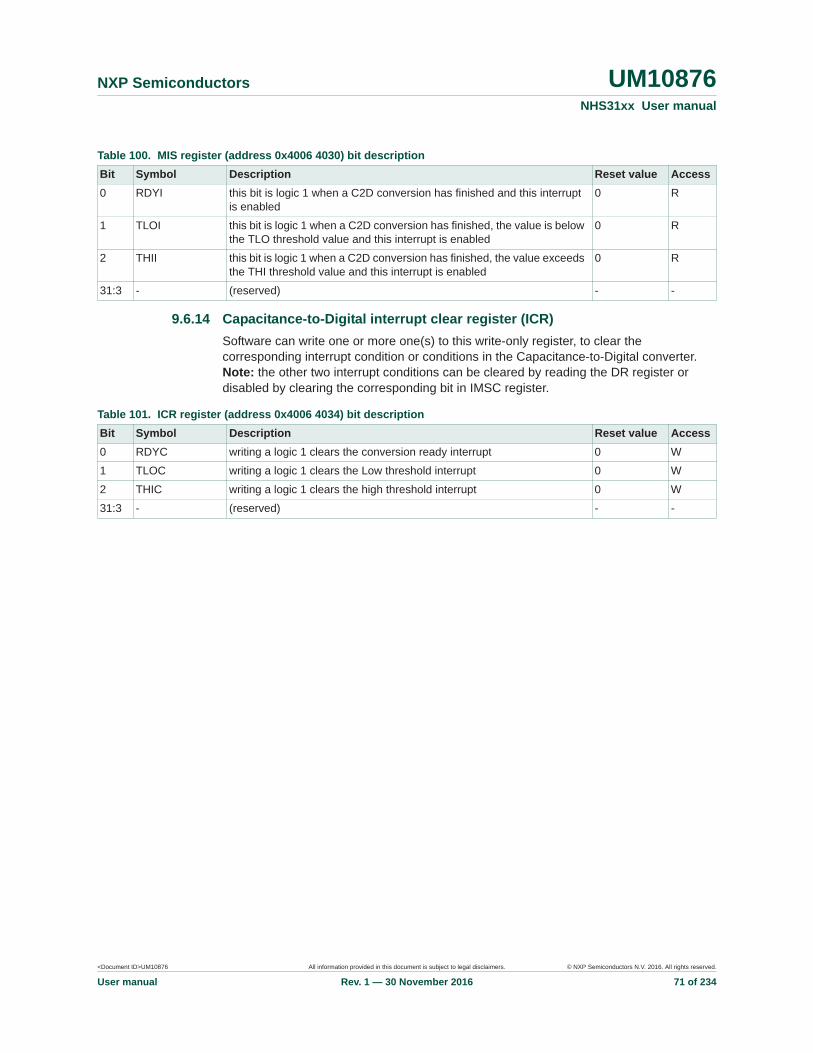
<Document ID>UM10876 All information provided in this document is subject to legal disclaimers. © NXP Semiconductors N.V. 2016. All rights reserved.
User manual Rev. 1 — 30 November 2016 71 of 234
NXP Semiconductors UM10876NHS31xx User manual
9.6.14 Capacitance-to-Digital interrupt clear register (ICR)Software can write one or more one(s) to this write-only register, to clear the corresponding interrupt condition or conditions in the Capacitance-to-Digital converter. Note: the other two interrupt conditions can be cleared by reading the DR register or disabled by clearing the corresponding bit in IMSC register.
Table 100. MIS register (address 0x4006 4030) bit descriptionBit Symbol Description Reset value Access0 RDYI this bit is logic 1 when a C2D conversion has finished and this interrupt
is enabled0 R
1 TLOI this bit is logic 1 when a C2D conversion has finished, the value is below the TLO threshold value and this interrupt is enabled
0 R
2 THII this bit is logic 1 when a C2D conversion has finished, the value exceeds the THI threshold value and this interrupt is enabled
0 R
31:3 - (reserved) - -
Table 101. ICR register (address 0x4006 4034) bit descriptionBit Symbol Description Reset value Access0 RDYC writing a logic 1 clears the conversion ready interrupt 0 W
1 TLOC writing a logic 1 clears the Low threshold interrupt 0 W
2 THIC writing a logic 1 clears the high threshold interrupt 0 W
31:3 - (reserved) - -
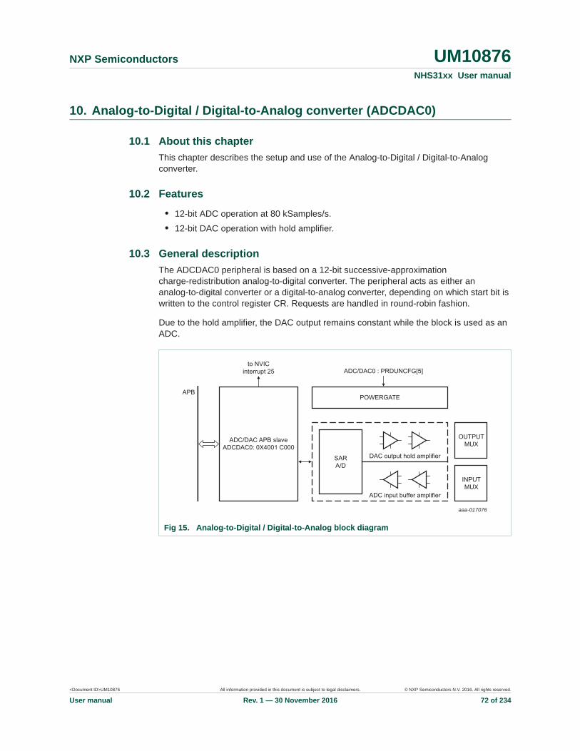
<Document ID>UM10876 All information provided in this document is subject to legal disclaimers. © NXP Semiconductors N.V. 2016. All rights reserved.
User manual Rev. 1 — 30 November 2016 72 of 234
NXP Semiconductors UM10876NHS31xx User manual
10. Analog-to-Digital / Digital-to-Analog converter (ADCDAC0)
10.1 About this chapterThis chapter describes the setup and use of the Analog-to-Digital / Digital-to-Analog converter.
10.2 Features
• 12-bit ADC operation at 80 kSamples/s.• 12-bit DAC operation with hold amplifier.
10.3 General descriptionThe ADCDAC0 peripheral is based on a 12-bit successive-approximation charge-redistribution analog-to-digital converter. The peripheral acts as either an analog-to-digital converter or a digital-to-analog converter, depending on which start bit is written to the control register CR. Requests are handled in round-robin fashion.
Due to the hold amplifier, the DAC output remains constant while the block is used as an ADC.
Fig 15. Analog-to-Digital / Digital-to-Analog block diagram
aaa-017076
ADC/DAC APB slaveADCDAC0: 0X4001 C000
to NVICinterrupt 25
APB
ADC/DAC0 : PRDUNCFG[5]
POWERGATE
DAC output hold amplifier
OUTPUTMUX
INPUTMUX
ADC input buffer amplifier
SARA/D

<Document ID>UM10876 All information provided in this document is subject to legal disclaimers. © NXP Semiconductors N.V. 2016. All rights reserved.
User manual Rev. 1 — 30 November 2016 73 of 234
NXP Semiconductors UM10876NHS31xx User manual
10.4 Input multiplexer and output switch matrixThe ADC input and DAC output are connected to the analog buses and on-chip transducers via an analog multiplexer. Table 102 shows the connections of the multiplexer.
Table 102. Connections to ADC input and output multiplexersAMUX input Source / target Description0 ana_extbus0 (external) pin ANA0_0
1 ana_extbus1 (external) pin ANA0_1
2 ana_extbus2 (external) pin ANA0_2
3 ana_extbus3 (external) pin ANA0_3
4 ana_extbus4 (external) pin ANA0_4
5 ana_extbus5 (external) pin ANA0_5
6 (reserved) (reserved)
7 (reserved) (reserved)
8 (reserved) (reserved)
9 (reserved) (reserved)
10 (reserved) (reserved)
11 (reserved) (reserved)
<Document ID>UM10876 All information provided in this document is subject to legal disclaimers. © NXP Semiconductors N.V. 2016. All rights reserved.
User manual Rev. 1 — 30 November 2016 74 of 234
NXP Semiconductors UM10876NHS31xx User manual
10.5 Register descriptionsThe register addresses for the Analog-to-Digital / Digital-to-Analog converter are listed in Table 103.
[1] Reset Value reflects the data stored in used bits only. It does not include content of reserved bits.
10.5.1 ADC Control register (CR)The ADCDAC control register controls the operation of the SAR ADC/DAC.
10.5.2 ADC Data register (ADCDR)The ADCDR register holds a value proportional to the measured voltage as determined by the Analog-to-Digital converter.
Table 103. Register overview: Analog-to-Digital / Digital-to-Analog converter (base address 0x4001 C000)Name Access Address
offsetDescription Reset value[1]
CR R/W 0x000 control register 0x0000 0000
ADCDR R 0x004 ADC Data register. Contains result of Analog-to-Digital conversion
0x0000 0000
DACDR W 0x008 DAC Data register. Contains value to be converted to analog voltage
0x0000 0000
SP0 R/W 0x010 ADCDAC setup register 0x0000 0000
ADCMUX R/W 0x018 ADC input multiplexer setting 0x0000 0000
DACMUX R/W 0x01C DAC output switch setting 0x0000 0000
ADCTLO R/W 0x020 low value threshold register 0x0000 0000
ADCTHI R/W 0x024 high value threshold register 0x0000 0000
IMSC R/W 0x028 interrupt Mask Set and Clear register 0x0000 0000
RIS R 0x02C raw Interrupt Status register 0x0000 0008
MIS R 0x030 masked Interrupt Status register 0x0000 0000
ICR W 0x034 interrupt Clear register n/a
Table 104. CR register (address 0x4001 C000) bit descriptionBit Symbol Description Reset value Access0 ADCSTART start bit for Analog-to-Digital conversion. ADCDAC clears this bit at the
end of the measurement0 R/W
1 DACSTART start bit for Digital-to-Analog conversion. When the analog level is available on the output bus, the ADCDAC clears this bit
0 R/W
2 ADCCONT set ADC to Continuous mode 0 R/W
3 DACCONT set DAC to Continuous mode 0 R/W
4 ADCSTOP stop ADC conversion after current conversion (in Continuous mode) 0 R/W
5 DACSTOP stop DAC conversion after current conversion (in Continuous mode) 0 R/W
31:6 - (reserved) - -
Table 105. ADCDR register (address 0x4001 C004) bit descriptionBit Symbol Description Reset value Access11:0 ADCDATA result of last conversion, unsigned 12-bit integer 0x000 R
31:12 - (reserved) - -
<Document ID>UM10876 All information provided in this document is subject to legal disclaimers. © NXP Semiconductors N.V. 2016. All rights reserved.
User manual Rev. 1 — 30 November 2016 75 of 234
NXP Semiconductors UM10876NHS31xx User manual
10.5.3 DAC Data register (DACDR)The DACDR register holds the value to be converted to a voltage. This conversion will occur at the next write of the DACSTART bit in the CR register.
10.5.4 ADC Status register (SR)The ADCSR register holds the status of the ADCDAC.
10.5.5 ADCDAC Setup register (ADCSP)The ADCSP register holds the setup of the ADC.
Table 106. DACDR register (address 0x4001 C008) bit descriptionBit Symbol Description Reset value Access11:0 DACDATA value to be converted to voltage, unsigned 12-bit integer 0x000 R
31:12 - (reserved) - -
Table 107. SR register (address 0x4001 C00C) bit descriptionBit Symbol Description Reset value Access31:0 - (reserved) - -
Table 108. ADCSP register (address 0x4001 C010) bit descriptionBit Symbol Value Description Reset value Access0 ADOFFSETCAL - measurement reference voltage. Setting should correspond
to ADC input range setting.1 R/W
0 0.5 V
1 0.9 V
1 ADWIDERANGE - input range 1 R/W
0 0 - 1 V
1 0 - 1.6 V
2 BOOSTSUPREF 1 boost the drive capability of the reference/supply buffers 0 R/W
3 CURRBACKUP 1 enable additional bias current within the reference block 0 R/W
4 LESSSLEW 1 boost current and therefore the speed of DAC output 0 R/W
5 SLOWCLK 1 reduce overall speed of ADCDAC 0 R/W
6 DYNAMICSLP 1 reduce the power of input and output amp if they are not used immediately
0 R/W
7 BOOSTINAMP 1 boost current and therefore speed of ADC input amplifier 0 R/W
8 BOOSTOUTAMP 1 boost current and therefore speed of DAC output amplifier 0 R/W
9 ONEACTIVE 1 disable the non-selected function (ADC or DAC) 0 R/W
31:10 - - (reserved) - -

<Document ID>UM10876 All information provided in this document is subject to legal disclaimers. © NXP Semiconductors N.V. 2016. All rights reserved.
User manual Rev. 1 — 30 November 2016 76 of 234
NXP Semiconductors UM10876NHS31xx User manual
10.5.6 ADC Input Multiplexer register (ADCMUX)ADCMUX holds the settings for the input multiplexers.
10.5.7 DAC Output switch register (DACMUX)DACSW holds the settings for the output switch matrix.
10.5.8 ADCDAC low-value threshold register (ADCTLO)ADCTLO contains the low threshold value. The measured bit value is compared to this value. If the measured value is lower, and the corresponding bit in the ADCIMSC register is set, an interrupt is generated.
10.5.9 ADCDAC high-value threshold register (ADCTHI)ADCTHI contains the low threshold value. The measured bit value is compared to this value. If the measured value is higher, and the corresponding bit in the ADCIMSC register is set, an interrupt is generated.
10.5.10 ADCDAC Interrupt Mask Set/Clear register (IMSC)This register controls whether each of the three possible interrupt conditions in the ADC are enabled.
Table 109. ADCMUX register (address 0x4001 C018) bit descriptionBit Symbol Value Description Reset value Access19:0 ADCMUX - each bit represents an input of the switching matrix 0 R/W
0 disconnected
1 connected to input
31:20 - - (reserved) - -
Table 110. DACMUX register (address 0x4001 C01C) bit descriptionBit Symbol Value Description Reset value Access19:0 DACSW - each bit represents an input of the switching matrix 0 R/W
0 disconnected
1 connected to input
31:20 - - (reserved) - -
Table 111. ADCTLO register (address 0x4001 C020) bit descriptionBit Symbol Description Reset value Access15:0 ADCTLO low threshold value 0x0000 R/W
31:16 - (reserved) - -
Table 112. ADC0THI register (address 0x4001 C024) bit descriptionBit Symbol Description Reset value Access15:0 ADCTHI high threshold value 0x0000 R/W
31:16 - (reserved) - -

<Document ID>UM10876 All information provided in this document is subject to legal disclaimers. © NXP Semiconductors N.V. 2016. All rights reserved.
User manual Rev. 1 — 30 November 2016 77 of 234
NXP Semiconductors UM10876NHS31xx User manual
10.5.11 ADCDAC Raw Interrupt Status register (RIS)This read-only register contains a logic 1 for each interrupt condition that is asserted, regardless of whether the interrupt is enabled in the IMSC register.
10.5.12 ADCDAC Masked Interrupt Status register (MIS)This read-only register contains a logic 1 for each interrupt condition that is asserted and enabled in the IMSC register. When an ADCDAC interrupt occurs, the interrupt service routine should read this register to determine the cause or causes of the interrupt.
Table 113. IMSC register (address 0x4001 C028) bit descriptionBit Symbol Description Reset value Access0 DACRDYI software should set this bit to enable interrupt when the DAC finished a
conversion0 R/W
1 ADCRDYI software should set this bit to enable interrupt when an ADC conversion value is ready in ADCDR
0 R/W
2 ADCLO software should set this bit to enable interrupt when the value of the conversion is lower than the value stored in ADCTLO
0 R/W
3 ADCHI software should set this bit to enable interrupt when the value of the conversion is higher than the value stored in ADCTHI
0 R/W
31:4 - (reserved) - -
Table 114. RIS register (address 0x4001 C02C) bit descriptionBit Symbol Description Reset value Access0 DACRDYI this bit is logic 1 when a D/A conversion has finished 0 R
1 ADCRDYI this bit is logic 1 when an A/D conversion has finished 0 R
2 ADCLOI this bit is logic 1 when an A/D conversion has finished and the value is below the threshold value set in the ADCTLO register
0 R
3 ADCHII this bit is logic 1 when an A/D conversion has finished and the value exceeds the threshold value set in the ADCTHI register
0 R
31:4 - (reserved) - -
Table 115. MIS register (address 0x4001 C030) bit descriptionBit Symbol Description Reset value Access0 DACRDYI this bit is logic 1 when a D/A conversion has finished and this interrupt is
enabled0 R
1 ADCRDYI this bit is logic 1 when an A/D conversion has finished and this interrupt is enabled
0 R
2 ADCLOI this bit is logic 1 when an A/D conversion has finished, the value is below the ADCTLO threshold value and this interrupt is enabled
0 R
3 ADCHII this bit is logic 1 when an A/D conversion has finished, the value exceeds the ADCTHI threshold value and this interrupt is enabled
0 R
31:4 - (reserved) - -

<Document ID>UM10876 All information provided in this document is subject to legal disclaimers. © NXP Semiconductors N.V. 2016. All rights reserved.
User manual Rev. 1 — 30 November 2016 78 of 234
NXP Semiconductors UM10876NHS31xx User manual
10.5.13 ADCDAC Interrupt Clear register (ICR)Software can write one or more logic 1s to this write-only register, to clear the corresponding interrupt condition or conditions in the Capacitance-to-Digital converter. Note: the other two interrupt conditions can be cleared by reading the ADCDR register or disabled by clearing the corresponding bit in the IMSC register.
Table 116. ADC0ICR register (address 0x4001 C034) bit descriptionBit Symbol Description Reset value Access0 DACRDYIC writing a logic 1 clears the D/A conversion ready interrupt 0 W
1 ADCRDYC writing a logic 1 clears the A/D conversion ready interrupt 0 W
2 ADCLOC writing a logic 1 clears the low threshold interrupt 0 W
3 ADCHIC writing a logic 1 clears the high threshold interrupt 0 W
31:4 - (reserved) - -
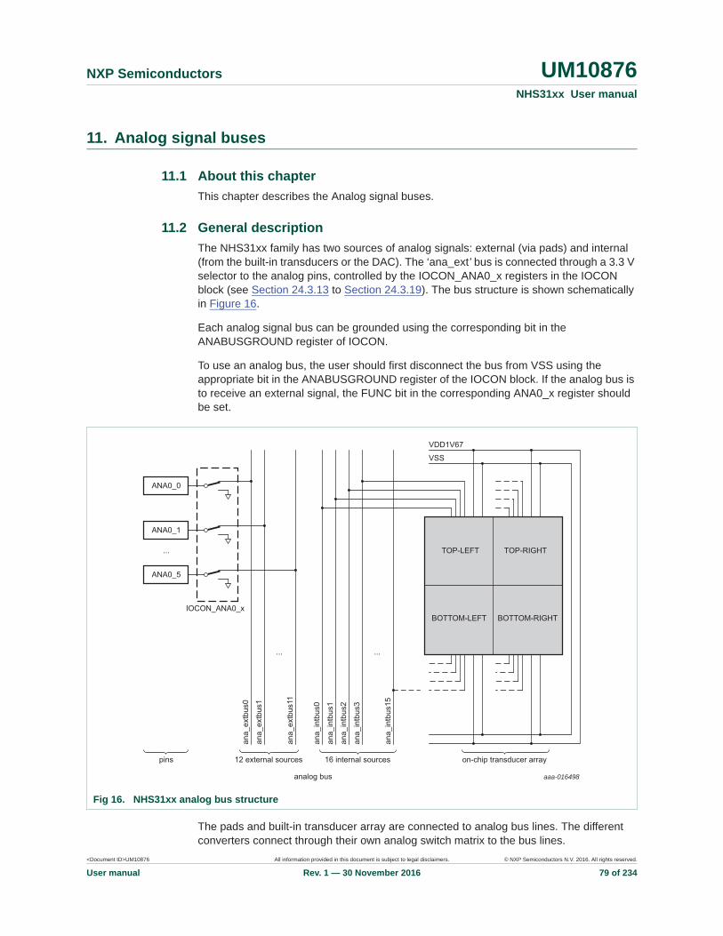
<Document ID>UM10876 All information provided in this document is subject to legal disclaimers. © NXP Semiconductors N.V. 2016. All rights reserved.
User manual Rev. 1 — 30 November 2016 79 of 234
NXP Semiconductors UM10876NHS31xx User manual
11. Analog signal buses
11.1 About this chapterThis chapter describes the Analog signal buses.
11.2 General descriptionThe NHS31xx family has two sources of analog signals: external (via pads) and internal (from the built-in transducers or the DAC). The ‘ana_ext’ bus is connected through a 3.3 V selector to the analog pins, controlled by the IOCON_ANA0_x registers in the IOCON block (see Section 24.3.13 to Section 24.3.19). The bus structure is shown schematically in Figure 16.
Each analog signal bus can be grounded using the corresponding bit in the ANABUSGROUND register of IOCON.
To use an analog bus, the user should first disconnect the bus from VSS using the appropriate bit in the ANABUSGROUND register of the IOCON block. If the analog bus is to receive an external signal, the FUNC bit in the corresponding ANA0_x register should be set.
The pads and built-in transducer array are connected to analog bus lines. The different converters connect through their own analog switch matrix to the bus lines.
Fig 16. NHS31xx analog bus structure
aaa-016498
ANA0_0
ANA0_1
ANA0_5
IOCON_ANA0_x
ana_
extb
us0
ana_
extb
us1
ana_
extb
us11
ana_
intb
us0
ana_
intb
us1
ana_
intb
us2
ana_
intb
us3
ana_
intb
us15
12 external sources 16 internal sources
analog bus
on-chip transducer array
...
... ...
TOP-LEFT
VDD1V67
VSS
BOTTOM-LEFT
TOP-RIGHT
BOTTOM-RIGHT
pins

<Document ID>UM10876 All information provided in this document is subject to legal disclaimers. © NXP Semiconductors N.V. 2016. All rights reserved.
User manual Rev. 1 — 30 November 2016 80 of 234
NXP Semiconductors UM10876NHS31xx User manual
12. RFID/NFC communication unit
12.1 About this chapterThis chapter describes the use of the RFID/NFC Communication unit.
12.2 IntroductionNear Field Communication (NFC) is a technology that enables smartphones, and many other devices, to establish radio communication by bringing them into close proximity. Typically NFC has a range of 10 cm (3.9 in) or less.
12.3 Features
• ISO/IEC 14443 A 1-3 compatible• MIFARE (Ultralight) compatible• NFC Forum Type 2 compatible• Easy interfacing with standard user memory space READ/WRITE commands• Passive operation possible• 50 pF internal capacitance for compatibility with standard NFC antennas
12.4 General descriptionThe RFID/NFC interface allows communication using 13.56 MHz proximity signaling. It is based on the MIFARE Ultralight EV1 PICC. The RFID interface works internally at 6.78 MHz. This clock is recovered from the RF field and is independent of the NHS31xx system clock.
The CMDIN, CMDOUT, SR and SRAM are mapped in the user memory space of the RFID core. The RFID READ and WRITE commands allows wireless communication via this shared memory. By only allowing access after password authentication by the MIFARE protocol, the READ/WRITE operation can be blocked.
Fig 17. Block diagram of the RFID/NFC interface
aaa-015354
RFIDANALOG
INTERFACE
EEPROMSUBSYSTEM
SRAM
APBINTERFACE
CMDIN
DATAOUT
SR Register
APB SLAVE SUBSYSTEM irq
APB
RFID DIGITAL SUBSYSTEM
VDD_RFID
EEPROMINTERFACE
RFIDMAIN
CONTROLLER
RFIDANALOG
SUBSYSTEM
LA
LB
TP
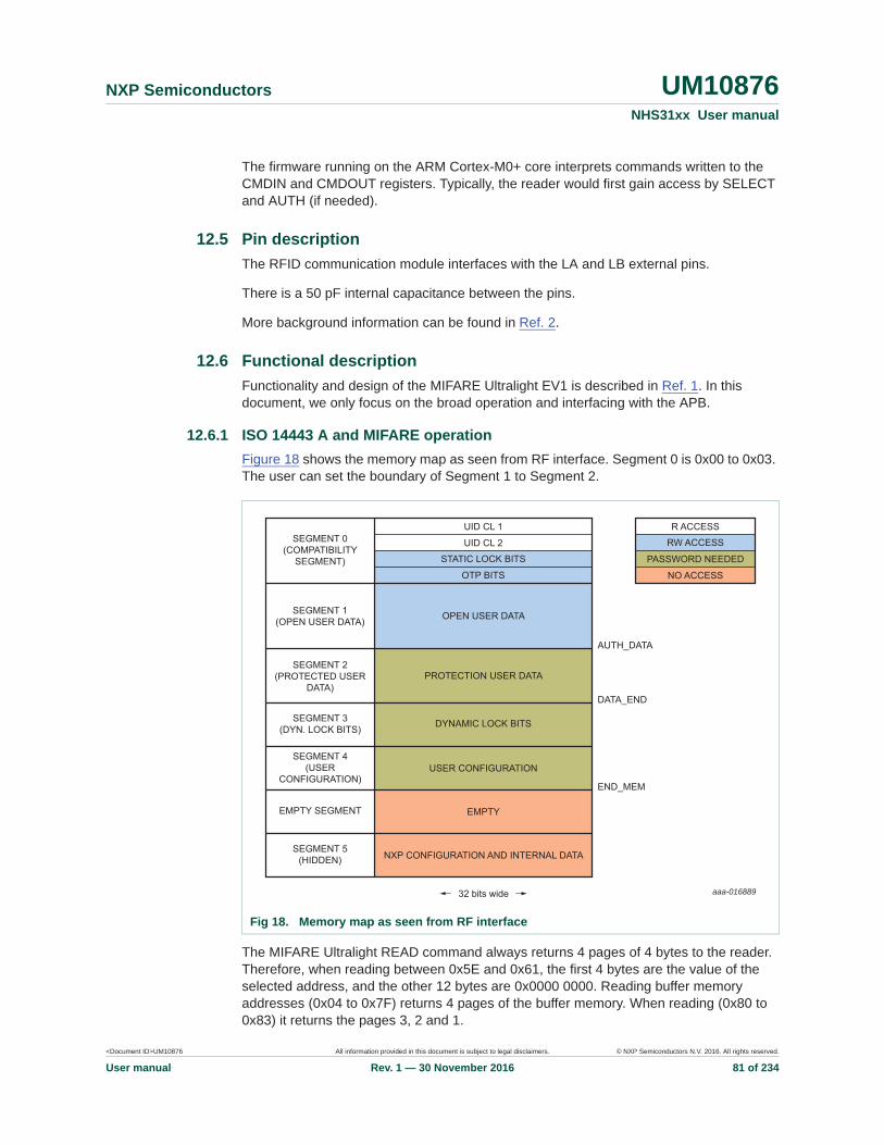
<Document ID>UM10876 All information provided in this document is subject to legal disclaimers. © NXP Semiconductors N.V. 2016. All rights reserved.
User manual Rev. 1 — 30 November 2016 81 of 234
NXP Semiconductors UM10876NHS31xx User manual
The firmware running on the ARM Cortex-M0+ core interprets commands written to the CMDIN and CMDOUT registers. Typically, the reader would first gain access by SELECT and AUTH (if needed).
12.5 Pin descriptionThe RFID communication module interfaces with the LA and LB external pins.
There is a 50 pF internal capacitance between the pins.
More background information can be found in Ref. 2.
12.6 Functional descriptionFunctionality and design of the MIFARE Ultralight EV1 is described in Ref. 1. In this document, we only focus on the broad operation and interfacing with the APB.
12.6.1 ISO 14443 A and MIFARE operationFigure 18 shows the memory map as seen from RF interface. Segment 0 is 0x00 to 0x03. The user can set the boundary of Segment 1 to Segment 2.
The MIFARE Ultralight READ command always returns 4 pages of 4 bytes to the reader. Therefore, when reading between 0x5E and 0x61, the first 4 bytes are the value of the selected address, and the other 12 bytes are 0x0000 0000. Reading buffer memory addresses (0x04 to 0x7F) returns 4 pages of the buffer memory. When reading (0x80 to 0x83) it returns the pages 3, 2 and 1.
Fig 18. Memory map as seen from RF interface
aaa-016889
SEGMENT 0(COMPATIBILITY
SEGMENT)
SEGMENT 1(OPEN USER DATA) OPEN USER DATA
AUTH_DATA
DATA_END
32 bits wide
END_MEM
UID CL 1 R ACCESS
RW ACCESS
PASSWORD NEEDED
NO ACCESS
UID CL 2
OTP BITS
STATIC LOCK BITS
PROTECTION USER DATA
DYNAMIC LOCK BITS
USER CONFIGURATION
EMPTY
NXP CONFIGURATION AND INTERNAL DATASEGMENT 5
(HIDDEN)
SEGMENT 4(USER
CONFIGURATION)
EMPTY SEGMENT
SEGMENT 2(PROTECTED USER
DATA)
SEGMENT 3(DYN. LOCK BITS)
<Document ID>UM10876 All information provided in this document is subject to legal disclaimers. © NXP Semiconductors N.V. 2016. All rights reserved.
User manual Rev. 1 — 30 November 2016 82 of 234
NXP Semiconductors UM10876NHS31xx User manual
The remaining pages of the buffer are padded by 0x0000 0000. This padding is to avoid accessing the memory space beyond END_MEM. It is possible to FAST_READ pages 0x04 to 0x83. The MIFARE Ultralight WRITE command writes to one page by default. The COMP_WRITE command sends 16 data bytes to the NHS31xx, but only the least significant 4 bytes are written to the addressed page.
12.6.2 NHS31xx family communication protocolCommunication between the RFID/NFC reader and the NHS31xx is initiated once the reader selects NHS31xx via ISO14443 commands. Access to the shared memory space is arbitrated between the RF side and the APB side by the arbitration unit. RFID-EEPROM access is only possible from RFID the side, and only for addresses not masked by the shared memory or the shared registers.
The reader can execute READ or WRITE commands on the shared memory or on the registers. Interpretation of the communication / messages written to the SRAM is done by firmware.
12.7 Register descriptions Data is stored in a communication buffer of 4 kbit (128 4 bytes), while commands are read or written from/to the CMDIN and CMDOUT registers.
The reset values reflect the data stored in used bits only, it does not include the content of reserved bits. The addresses of the SR, CMDIN, CMDOUT, and buffer memory are different when seen from APB (Table 117) or RFID side (Table 118).
Table 117. RFID/NFC communication block register and buffer memory space overview: APB sideName Access Address
offsetDescription Reset value
CFG R/W 0x000 RFID/NFC configuration register 0x0000 0000
SR R 0x004 RFID/NFC status register 0x0000 0000
CMDIN R 0x008 RFID/NFC incoming command 0x0000 0000
CMDOUT R/W 0x00C RFID/NFC outgoing command 0x0000 0000
TARGET R/W 0x010 RFID/NFC target page address register 0x0000 0004
LAST_ACCESS R 0x014 raw Interrupt status register 0x0000 0000
IMIS R/W 0x018 interrupt mask register 0x0000 0000
RIS R 0x01C raw Interrupt status register 0x0000 0000
MIS R 0x020 masked interrupt status register 0x0000 0000
IC W 0x024 interrupt clear register 0x0000 0000
SHARED_MEM R/W 0x100 -0x2FC
buffer memory space (128 words) undefined
Table 118. RFID/NFC communication block special registers and buffer memory space overview: RFID sideName Access Address
offsetDescription Reset value
SHARED_MEM R/W 0x04 -0x83
buffer memory space (128 words) 0
<Document ID>UM10876 All information provided in this document is subject to legal disclaimers. © NXP Semiconductors N.V. 2016. All rights reserved.
User manual Rev. 1 — 30 November 2016 83 of 234
NXP Semiconductors UM10876NHS31xx User manual
12.7.1 RFID/NFC configuration register (CFG)This register contains the configuration data for the RFID block
12.7.2 RFID/NFC status register (SR)This register contains the status of the RFID block.
SR R 0x84 RFID/NFC status register 0x0000 0000
CMDIN R/W 0x85 RFID/NFC incoming command 0x0000 0000
CMDOUT R 0x86 RFID/NFC outgoing data 0x0000 0000
Table 118. RFID/NFC communication block special registers and buffer memory space overview: RFID sideName Access Address
offsetDescription Reset value
Table 119. CFG register (address 0x4005 8000) bit descriptionBit Symbol Description Reset
valueAccess
0 BYPASS when set, the shared memory interface and registers are deactivated, and the external reader gets full access to the RFID/NFC EEPROM.
0 R/W
31:1 - (reserved) 0 -
Table 120. SR register (APB address 0x4005 8004, RF address 0x84) bit descriptionBit Symbol Description Reset
valueAccess
0 POR power-on detected in the RFID analog core 0 R
1 1V2 rectifier < 1.2 V output warning 0 R
2 1V5 rectifier < 1.5 V output warning 0 R
3 PLL RFID PLL locked 0 R
4 SEL RFID selected 0 R
5 AUTH RFID password for access authenticated 0 R
6 BYPASS RFID interface in Bypass mode 0 R
7 - (reserved) 0 R
<Document ID>UM10876 All information provided in this document is subject to legal disclaimers. © NXP Semiconductors N.V. 2016. All rights reserved.
User manual Rev. 1 — 30 November 2016 84 of 234
NXP Semiconductors UM10876NHS31xx User manual
[1] Read access from RFID side, Write access from APB side.
12.7.3 RFID/NFC incoming command register (CMDIN)This register contains an NHS3-specific incoming command. Reading this register by the ARM clears the corresponding interrupt. This register is writable through the RFID wireless interface.
12.7.4 RFID/NFC outgoing data register (CMDOUT)This register contains NHS3-specific outgoing data. This register can be read over the RFID wireless interface.
12.7.5 RFID/NFC target address register (TARGET)This register contains an NHS3-specific outgoing command. This register can be read over the RFID wireless interface.
15:8 RFID_CMD_ opcode of last RFID command received: 0 R
0000 0000: REQA
0000 0001: WUPA
0000 0010: ANTICOLLISION
0000 0011: SELECT
0000 0100: HLTA
0000 0101: READ
0000 0110: COMP_WRITE
0000 0111: WRITE
0000 1000: INCR_CNT
0000 1001: READ_CNT
0000 1010: PWD_AUTH
0000 1011: GET_VERSION
0000 1100: FAST_READ
0000 1101: READ_SIG
0000 1111: CHECK_TEARING_EVENT
31:12 - (reserved) - -
Table 120. SR register (APB address 0x4005 8004, RF address 0x84) bit description _continued
Bit Symbol Description Reset value
Access
Table 121. CMDIN register (APB address 0x4005 800C, RF address 0x85) bit descriptionBit Symbol Description Reset value Access31:0 CMDIN incoming command 0x0000 0000 R
Table 122. CMDOUT register (APB address 0x4005 8010, RF address 0x86) bit descriptionBit Symbol Description Reset value Access31:0 CMDOUT outgoing data 0x0000 0000 R/W

<Document ID>UM10876 All information provided in this document is subject to legal disclaimers. © NXP Semiconductors N.V. 2016. All rights reserved.
User manual Rev. 1 — 30 November 2016 85 of 234
NXP Semiconductors UM10876NHS31xx User manual
12.7.6 RFID/NFC last accessed address register (LAST_ACCESS)This register contains the address of the last accessed pages. This address is an address as seen from the RF side. Both start and end of read/write address range are shown.
12.7.7 RFID/NFC interrupt mask register (IMSC)This register controls whether RFID read/write access interrupt condition is enabled.
12.7.8 RFID/NFC Raw interrupt status register (RIS)This read-only register contains a 1 for each interrupt condition that is asserted, regardless of whether the interrupt is enabled in the IMSC register.
Table 123. TARGET register (address 0x4005 8010) bit descriptionBit Symbol Description Reset value Access7:0 PAGE target (RF) page address 0x04 R/W
31:8 - (reserved) 0 -
Table 124. LAST_ACCESS register (address 0x4005 8014) bit descriptionBit Symbol Description Reset value Access7:0 LAST_ACCESS_END last accessed (RF) page address (end of range) 0 R
15:8 LAST_ACCESS_START last accessed (RF) page address (start of range) 0 R
16 DIR direction of last accessed page (0) READ, (1) WRITE 0 R
31:17 - (reserved) 0 -
Table 125. IMSC register (address 0x4005 8014) bit descriptionBit Symbol Description Reset value Access0 RFPOWER set to enable interrupt when RFID power is detected 0 R/W
1 RFSELECT set to enable interrupt when reader selects tag 0 R/W
2 MEMREAD set to enable interrupt when reader reads from shared memory (SHARED_MEM)
0 R/W
3 MEMWRITE set to enable interrupt when reader writes to shared memory (SHARED_MEM)
0 R/W
4 CMDWRITE set to enable interrupt when reader writers to CMDIN register 0 R/W
5 CMDREAD set to enable interrupt when reader reads the CMDOUT register 0 R/W
6 TARGETWRITE set to enable interrupt when reader writes to address specified in the TARGET register
0 R/W
7 TARGETREAD set to enable interrupt when reader reads from address specified in the TARGET register
0 R/W
8 NFCOFF set to enable interrupt when external reader powers down RFID/NFC front-end
0 R/W
31:9 - (reserved) - -
Table 126. RIS register (address 0x4005 801C) bit descriptionBit Symbol Description Reset value Access0 RFPOWER RFID power is detected 0 R/W
1 RFSELECT reader selected tag 0 R/W
2 MEMREAD reader reads from shared memory (SHARED_MEM) 0 R/W
3 MEMWRITE reader writes to shared memory (SHARED_MEM) 0 R/W

<Document ID>UM10876 All information provided in this document is subject to legal disclaimers. © NXP Semiconductors N.V. 2016. All rights reserved.
User manual Rev. 1 — 30 November 2016 86 of 234
NXP Semiconductors UM10876NHS31xx User manual
12.7.9 RFID/NFC Raw interrupt status register (RIS)This read-only register contains a 1 for each interrupt condition that is asserted, regardless of whether the interrupt is enabled in the IMSC register.
12.7.10 RFID/NFC Interrupt clear register (ICR)Software can write one or more one(s) to this write-only register to clear the corresponding interrupt condition or conditions in the RFID/NFC controller. Note: the second interrupt conditions can be cleared by reading the CMDIN register.
4 CMDWRITE reader writers to CMDIN register 0 R/W
5 CMDREAD reader reads the CMDOUT register 0 R/W
6 TARGETWRITE reader writes to address specified in the TARGET register 0 R/W
7 TARGETREAD reader reads from address specified in the TARGET register 0 R/W
8 NFCOFF RFID/NFC front-end is not powered or clocked 0 R/W
31:9 - (reserved) 0 -
Table 126. RIS register (address 0x4005 801C) bit description _continued
Bit Symbol Description Reset value Access
Table 127. RIS register (address 0x4005 801C) bit descriptionBit Symbol Description Reset value Access0 RFPOWER RFID power is detected 0 R/W
1 RFSELECT reader selects tag 0 R/W
2 MEMREAD reader reads from shared memory (SHARED_MEM) 0 R/W
3 MEMWRITE reader writes to shared memory (SHARED_MEM) 0 R/W
4 CMDWRITE reader writers to CMDIN register 0 R/W
5 CMDREAD reader reads the CMDOUT register 0 R/W
6 TARGETWRITE reader writes to address specified in the TARGET register 0 R/W
7 TARGETREAD reader reads from address specified in the TARGET register 0 R/W
8 NFCOFF RFID/NFC front-end is not powered or clocked 0 R/W
31:9 - (reserved) 0 -
Table 128. ICR register (address 0x4005 8024) bit descriptionBit Symbol Description Reset value Access0 RFPOWER write logic 1 to clear RFPOWER interrupt 0 W
1 RFSELECT write logic 1 to clear RFSELECT interrupt 0 W
2 MEMREAD write logic 1 to clear MEMREAD interrupt 0 W
3 MEMWRITE write logic 1 to clear MEMWRITE interrupt 0 W
4 CMDWRITE write logic 1 to clear CMDWRITE interrupt 0 W
5 CMDREAD write logic 1 to clear CMDREAD interrupt 0 W
6 TARGETWRITE write logic 1 to clear TARGETWRITE interrupt 0 W
7 TARGETREAD write logic 1 to clear TARGETREAD interrupt 0 W
8 NFCOFF write logic 1 to clear NFCOFF interrupt 0 W
31:9 - (reserved) 0 -
<Document ID>UM10876 All information provided in this document is subject to legal disclaimers. © NXP Semiconductors N.V. 2016. All rights reserved.
User manual Rev. 1 — 30 November 2016 87 of 234
NXP Semiconductors UM10876NHS31xx User manual
12.7.11 Buffer memoryThe buffer memory ranges from APB address 0x4005 8100 to 0x4005 82FC or RF address 0x04 to 0x83. The buffer memory is a regular 4 kB 32-bit Ultra-high VT SRAM memory block configured as x=64, y=2, z=1, b=32. The purpose of the buffer memory is to serve as an interface for the exchange of PHDC and/or NDEF messages. The buffer memory contains random data after reset. This memory is word-addressable only.
<Document ID>UM10876 All information provided in this document is subject to legal disclaimers. © NXP Semiconductors N.V. 2016. All rights reserved.
User manual Rev. 1 — 30 November 2016 88 of 234
NXP Semiconductors UM10876NHS31xx User manual
13. Real-Time clock
13.1 About this chapterThis chapter describes the usage of the Real Time Clock (RTC) timer.
The RTC timer is identical on all members of the NHS31xx family.
13.2 FeaturesThe Real Time Clock (RTC) timer provides a countdown timer generating a wake-up signal when it expires. The timer runs on a low speed clock and and is always active unless the VDDBAT is switched off.
The RTC timer generates the RTC interrupt signal (wake-up interrupt 12), which can be enabled according to the settings in the RTCIMSC register. The timer counts in "ticks" which are derived from the TFRO clock pulses via the calibration value stored in the RTCCAL register.
13.3 General descriptionThe RTC module consists of 3 parts:
1. The RTC core module, implementing the RTC timer itself. This module runs in the 'always on' VDD domain and is implemented in 3.3 V logic
2. The AMBA APB slave interface. This module allows configuration of the RTC core via an APB bus. This module runs in the switched power domain
3. Level-shifters. This module interconnects the core and the APB interface. It contains all level-shifters and isolation gates necessary to interconnect both modules
13.4 Register descriptionsThe CR register controls the RTC timer.
The reset values reflect the data stored in used bits only, they do not include the content of reserved bits.
Table 129. Register overview: RTC timer (base address 0x4005 4000)Name Access Address
offsetDescription Reset value
CR R/W 0x000 RTC control register 0x0000 0000
SR R 0x004 RTC status register 0x0000 0002
CAL R/W 0x008 RTC calibration value 0x0000 8000
SLEEPT R/W 0x00C RTC Sleep time 0x0000 0000
VAL R 0x010 current RTC counter 0x0000 0000
IMIS R/W 0x014 interrupt mask register 0x0000 0000
RIS R 0x018 raw Interrupt status register 0x0000 0000
MIS R 0x01C masked interrupt status register. 0x0000 0000

<Document ID>UM10876 All information provided in this document is subject to legal disclaimers. © NXP Semiconductors N.V. 2016. All rights reserved.
User manual Rev. 1 — 30 November 2016 89 of 234
NXP Semiconductors UM10876NHS31xx User manual
13.4.1 RTC Control register (CR)The CR register controls the operation of the RTC Timer unit. If the unit is disabled, nothing happens.
13.4.2 RTC status register (SR)The SR register shows the status of the RTC Timer unit. SR[1] is identical to PMU.TMRCLKCTRL[0].
For the RTC to count down time (RUN=1) the following conditions must be fulfilled:
1. it must be powered.2. it must be receiving 32 kHz pulses.3. it must be started.
13.4.3 RTC calibration register (CAL)The CAL register contains the number of TFRO clock pulses in one tick. When the CALIB value is reached, one tick is issued. Setting 1 tick equal to 1 second is recommended. The default is 32,768 clock pulses in one tick.
ICR W 0x020 interrupt clear register. 0x0000 0000
STAT R 0x024 access status register. 0x0000 0000
TIME R/W 0x030 RTC Time register. 0x0000 0000
Table 129. Register overview: RTC timer (base address 0x4005 4000) _continued
Name Access Addressoffset
Description Reset value
Table 130. RTC Timer control register (address 0x4005 4000) bit descriptionBit Symbol Description Reset value0 EN logic 1: Enable the RTC Timer, logic 0: disable 0
1 AUTOSTART logic 1: Automatic timer start when value is written to SLEEPT register, logic 0: manual start
1
2 START writing a logic 1 starts the countdown from the value stored in SLEEPT until logic 0 is reached. Write logic 0 to clear. This bit is also cleared when the interrupt is asserted or a new value is written into the SLEEPT register
0
31:3 - (reserved) 0
Table 131. RTC Timer status register (address 0x4005 4004) bit descriptionBit Symbol Description Reset value0 EN logic 1: RTC timer enabled, logic 0: disabled 0
1 - (reserved) 0
2 FREEZE asserted near to the edges of the internal tick clock. Values written to the SLEEPT register during FREEZE=1 are delayed until after this condition clears
0
3 RUN logic 1: RTC timer is running 0
31:4 - (reserved) 0
<Document ID>UM10876 All information provided in this document is subject to legal disclaimers. © NXP Semiconductors N.V. 2016. All rights reserved.
User manual Rev. 1 — 30 November 2016 90 of 234
NXP Semiconductors UM10876NHS31xx User manual
13.4.4 RTC timer sleep time register (SLEEPT) The SLEEPT register is set to the time in ticks the timer has to sleep. The timer unit decrements this value each tick and the RTC interrupt is generated whenever the value reaches zero. Writing this register triggers a start unless the AUTOSTART bit is cleared. Manual start or restart is possible by writing logic 1 to CR[2].
13.4.5 RTC timer current value register (VAL)The RTCVAL register contains the current remaining value of the timer in ticks.
13.4.6 RTC timer interrupt mask set/clear register (IE)This register controls whether the interrupt condition is enabled.
Note: ARM uses the word ‘masked’ in the opposite sense from classic computer terminology, in which 'masked' meant ‘disabled’. ARM uses the word 'masked' to mean ‘enabled’. To avoid confusion, we do not use the word ‘masked’.
13.4.7 RTC timer raw interrupt status register (RIS)This read-only register contains a logic 1 for each interrupt condition that is asserted, regardless of whether the interrupt is enabled in the IMSC register.
Table 132. RTC timer calibration register (address 0x4005 4008) bit descriptionBit Symbol Description Reset value15:0 CALIB this value indicates the number of TFRO clock pulses in
one tick8000h
31:16 - (reserved) 0
Table 133. RTC timer sleep time register (address 0x4005 400C) bit descriptionBit Symbol Description Reset value23:0 SLEEPTIME this value indicates the time to sleep in ticks 0
31:24 - (reserved) 0
Table 134. RTC timer current value register (address 0x4005 4010) bit descriptionBit Symbol Description Reset value23:0 TIMEREMAIN current value (remaining time) of the countdown timer 0
31:24 - (reserved) 0
Table 135. IMSC register (address 0x4005 4014) bit descriptionBit Symbol Description Reset
valueAccess
0 IE software should set this bit to enable interrupt when the countdown is finished
0 R/W
31:1 - (reserved) 0 -
Table 136. RIS register (address 0x4005 4018) bit descriptionBit Symbol Description Reset
valueAccess
0 RIS this bit is logic 1 when the countdown has finished 0 R
31:1 - (reserved) 0 -

<Document ID>UM10876 All information provided in this document is subject to legal disclaimers. © NXP Semiconductors N.V. 2016. All rights reserved.
User manual Rev. 1 — 30 November 2016 91 of 234
NXP Semiconductors UM10876NHS31xx User manual
13.4.8 RTC timer masked interrupt status register (MIS)This read-only register contains a logic 1 for each interrupt condition that is asserted and enabled in the IMSC registers. When an RTC interrupt occurs, the interrupt service routine should read this register to determine the cause or causes of the interrupt.
13.4.9 RTC timer interrupt clear register (ICR)Software can write one or more logic ones to this write-only register, to clear the corresponding interrupt condition in the RTC timer. Note: the interrupt conditions can be disabled by clearing the corresponding bit in IMSC registers.
13.4.10 RTC timer access status register (ACCSTAT)The access status register indicates whether the RTC is able to accept data over the APB. The RTC runs at a different clock rate than the core system, and bus synchronization is necessary. This mechanism is described below:
Write access
The write procedure is as follows:
• When the ARM writes to an RTC register:– The address/value pair is stored in the command-buffer– The direction flag is set to write– ACCCSTAT goes to logic 0 indicating a command is pending. This transition
happens on an edge of the APB clock, which is faster than the TFRO clock• When the TFRO clock edge comes, the address/value in the command-buffer is
written to the RTC block• On a next TFRO edge, the ACCSTAT goes to logic 0 to indicate that no command is
pending and a new one can be given
Read access
The read procedure is as follows:
• When a value is stored in the PMU register for the ARM to read:– only the register address is stored in the command-buffer– the direction flag is set to read
Table 137. MIS register (address 0x4005 401C) bit descriptionBit Symbol Description Reset
valueAccess
0 MIS this bit is logic 1 when the RTC countdown has finished and this interrupt is enabled
0 R
31:1 - (reserved) 0 -
Table 138. ICR register (address 0x4005 4020) bit descriptionBit Symbol Description Reset
valueAccess
0 IC writing a logic 1 clears the countdown done interrupt 0 W
31:1 - (reserved) 0 -

<Document ID>UM10876 All information provided in this document is subject to legal disclaimers. © NXP Semiconductors N.V. 2016. All rights reserved.
User manual Rev. 1 — 30 November 2016 92 of 234
NXP Semiconductors UM10876NHS31xx User manual
– ACCSTAT goes to logic 0 indicating a command is pending• When the TFRO clock edge arrives, the address in the buffer is used to read the
actual RTC register. This register value is copied in the (data part of the) command-buffer
• On the next TFRO edge, the ACCSTAT goes to logic 1 to indicate that the command is completed
• The command-buffer sees that the address of the second read is the same as the address part in the command-buffer. In this case, the result is not treated as a new read command ACCSTAT stays logic 1)
• However, the address part of the command-buffer is now cleared, so that a third read (even when from the same PMU register) causes a new command
13.4.11 RTC timer time register (TIME)The RTC time register contains a counter which is incremented at each timer tick (RTC must be clocked and enabled). A value can be written to this register by the user.
Table 139. ACCSTAT register (address 0x4005 4024) bit descriptionBit Symbol Description Reset
valueAccess
0 READY logic 0: RTC access not possible, logic 1: RTC access possible
0 R
31:1 - (reserved) 0 -
Table 140. TIME register (address 0x4005 4030) bit descriptionBit Symbol Description Reset
valueAccess
31:0 TIME current timer value 0 R/W
<Document ID>UM10876 All information provided in this document is subject to legal disclaimers. © NXP Semiconductors N.V. 2016. All rights reserved.
User manual Rev. 1 — 30 November 2016 93 of 234
NXP Semiconductors UM10876NHS31xx User manual
14. Watchdog timer
14.1 About this chapterThis chapter describes the watchdog timer, which is identical on all members of the NHS31xx family.
14.2 PurposeIf the microcontroller enters an erroneous state, the purpose of the Watchdog-timer (WDT) is to reset the microcontroller within a predetermined amount of time.
14.2.1 ConfigurationThe WDT is configured using the following:
• Pins: The WDT uses no external pins• Power: In the SYSAHBCLKCTRL register, set bit 11• Peripheral clock: Select the watchdog clock source and enable the WDT peripheral
clock by writing to the WDTCLKDIV register
14.2.2 Features
• Debug mode• Enabled by software but requires a hardware reset or a Watchdog reset/interrupt to be
disabled• If enabled, incorrect/incomplete feed sequence causes reset/interrupt• Flag to indicate Watchdog reset• Programmable 24-bit timer with internal pre-scaler• Selectable time period from (TWDCLK 256 4) to (TWDCLK 224 4) in multiples
of TWDCLK 4• The Watchdog clock (WDCLK) source is the 8 MHz oscillator (SFRO)
14.2.3 General descriptionRegister base address 0x4000 4000.
The Watchdog consists of a divide by 4 fixed pre-scaler and a 24-bit counter. The clock is fed to the timer via a pre-scaler. The timer decrements when clocked. The minimum value from which the counter decrements is 0xFF. Setting a value lower than 0xFF causes 0xFF to be loaded in the counter. Hence the minimum Watchdog interval is (TWDCLK 256 4) and the maximum is (TWDCLK 224 4), in multiples of (TWDCLK 4).
The Watchdog should be used in the following manner:
1. Set the Watchdog timer constant reload value in WDTC register2. Setup the Watchdog timer Operating mode in WDMOD register3. Enable the Watchdog by writing 0xAA followed by 0x55 to the WDFEED register4. The Watchdog should be fed again before the Watchdog counter underflows to
prevent a reset-interrupt

<Document ID>UM10876 All information provided in this document is subject to legal disclaimers. © NXP Semiconductors N.V. 2016. All rights reserved.
User manual Rev. 1 — 30 November 2016 94 of 234
NXP Semiconductors UM10876NHS31xx User manual
When the WDT is in Reset mode and the counter reaches zero, the CPU is reset and loads the stack pointer and program counter from the vector table. The same happens in the case of an external reset. The WDT timeout flag (WDTOF) can be examined to determine whether the WDT has caused the reset condition. Software must clear the WDTOF flag.
When the Watchdog is enabled (but not in Reset mode), the counter underflows, and the ARM M0+ core is in Sleep or Deep-sleep, the ARM wakes up.
The watchdog timer block uses two clocks: PCLK and WDCLK. PCLK is used for the APB accesses to the watchdog registers and is derived from the system clock (see Figure 3). The WDCLK is used for the watchdog timer counting and is derived from the wdt_clk. The SFRO is used as a clock source for wdt_clk clock. The WDCLK has its own clock divider which can also disable this clock.
There is some synchronization logic between these two clock domains. When APB operations update the WDMOD and WDTC registers, the new value takes effect in 3 WDCLK cycles on the logic in the WDCLK clock domain. When the watchdog timer is counting on WDCLK, the following procedure occurs: The synchronization logic locks the counter value on WDCLK and then synchronizes it with the PCLK for reading as the WDTV register by the CPU.
14.3 Register descriptionsThe Watchdog timer uses the registers shown in Table 141. More detailed descriptions follow.
14.3.1 Watchdog mode registerThe WDMOD register controls the operation of the Watchdog through the combination of WDEN and RESET bits. Note: a watchdog feed must be performed before any changes to the WDMOD register take effect.
Table 141. Register overview: Watchdog timer block (base address 0x4000 4000)Name Access Address
offsetDescription Reset value Reference
WDMOD R/W 0x000 Watchdog mode register. This register contains the Basic mode and status of the Watchdog Timer
0x0000 0000 -
WDTC R/W 0x004 watchdog timer constant register. This register determines the timeout value
0x0000 00FF -
WDFEED W 0x008 watchdog feed sequence register. Writing 0xAA followed by 0x55 to this register reloads the Watchdog timer with the value contained in WDTC
- -
WDTV R 0x00C watchdog timer value register. This register reads out the current value of the Watchdog timer
0x0000 00FF -

<Document ID>UM10876 All information provided in this document is subject to legal disclaimers. © NXP Semiconductors N.V. 2016. All rights reserved.
User manual Rev. 1 — 30 November 2016 95 of 234
NXP Semiconductors UM10876NHS31xx User manual
Once the WDEN and/or WDRESET bits are set, software cannot clear them. A reset or a Watchdog timer underflow clears both flags.
WDTOF — The Watchdog timeout flag is set when the Watchdog times out. Software or a POR reset clears this flag.WDINT — The Watchdog interrupt flag is set when the Watchdog times out. This flag is cleared when any reset occurs. Once the Watchdog interrupt is serviced, it should be disabled in the NVIC or the Watchdog interrupt request is generated indefinitely. The intent of the watchdog interrupt is to allow debugging Watchdog activity without resetting the device when the Watchdog overflows.
Watchdog reset or interrupt occurs any time the Watchdog is running and has an operating clock source. Any clock source works in Sleep mode, and if a Watchdog interrupt occurs in Sleep mode, it wakes the device.
14.3.2 Watchdog timer constant registerThe WDTC register determines the timeout value. Every time a feed sequence occurs the WDTC content is reloaded in to the Watchdog timer. It is a 32-bit register with 8 LSB set to logic 1 on reset. Writing values below 0xFF cause 0x0000 00FF to be loaded to the WDTC. Thus the minimum timeout interval is TWDCLK 256 4.
Table 142. WDMOD register (address 0x4000 4000) bit descriptionBit Symbol Description Reset value0 WDEN watchdog enable bit (Set Only). When logic 1, the watchdog
timer is running0
1 WDRESET watchdog reset enable bit (Set Only). When logic 1, a watchdog timeout causes a chip reset
0
2 WDTOF watchdog timeout flag. Set when the watchdog timer times out, cleared by software. (Read/write)
0
3 WDINT watchdog interrupt flag (Read Only, not clearable by software)
0
7:4 - (reserved) -
31:8 - (reserved) -
Table 143. Watchdog Operating mode selectionWDEN WDRESET Mode of operation0 debug/operate without the Watchdog running
1 0 Watchdog Interrupt mode: debug with the Watchdog interrupt but no WDRESET enabled. When this mode is selected, a Watchdog counter-underflow sets the WDINT flag and the Watchdog interrupt request is generated.Remark: In Interrupt mode, check the WDINT flag. If this flag is set, the interrupt is true and the interrupt routine can service it. If this flag is not set, the interrupt should be ignored
1 1 Watchdog Reset mode: operate with the Watchdog interrupt and WDRESET enabled. When this mode is selected, a Watchdog counter underflow resets the microcontroller. Although the Watchdog interrupt is also enabled in this case (WDEN = 1), it is not recognized because the Watchdog reset clears the WDINT flag

<Document ID>UM10876 All information provided in this document is subject to legal disclaimers. © NXP Semiconductors N.V. 2016. All rights reserved.
User manual Rev. 1 — 30 November 2016 96 of 234
NXP Semiconductors UM10876NHS31xx User manual
14.3.3 Watchdog feed registerWriting 0xAA followed by 0x55 to this register will reload the Watchdog timer with the WDTC value. This operation also starts the Watchdog if it is enabled via the WDMOD register. Setting the WDEN bit in the WDMOD register is not sufficient to enable the Watchdog. A valid feed sequence must be completed after setting WDEN before the Watchdog can generate a reset. Until then, the Watchdog ignores feed errors. After writing 0xAA to WDFEED, access to any Watchdog register other than writing 0x55 to WDFEED causes an immediate reset/interrupt when the Watchdog is enabled. The reset is generated during the second PCLK following incorrect access to a Watchdog register during a feed sequence.
Interrupts should be disabled during the feed sequence. If an interrupt happens during the feed sequence, then an abort condition occurs.
14.3.4 Watchdog timer value register
The WDTV register is used to read the current value of Watchdog timer. When reading the value of the 24-bit timer, the lock and synchronization procedure takes up to 6 WDCLK cycles plus 6 PCLK cycles. This procedure results in the value of WDTV being older than the actual value of the timer when the CPU is reading it.
Table 144. WDTC register (address 0x4000 4004) bit descriptionBit Symbol Description Reset value23:0 Count Watchdog timeout interval 0x0000 00FF
31:24 - (reserved) 0
Table 145. WDFEED register (address 0x4000 4008) bit descriptionBit Symbol Description Reset value0:7 Feed feed value should be 0xAA followed by 0x55 -
8:31 - (reserved) -
Table 146. WDTV register (address 0x4000 400C) bit descriptionBit Symbol Description Reset value23:0 Count counter-timer value 0x0000 00FF
31:24 - (reserved) -

<Document ID>UM10876 All information provided in this document is subject to legal disclaimers. © NXP Semiconductors N.V. 2016. All rights reserved.
User manual Rev. 1 — 30 November 2016 97 of 234
NXP Semiconductors UM10876NHS31xx User manual
15. SYSTICK timer
15.1 About this chapterThis chapter describes the SYSTICK timer, which is identical on all members of the NHS31xx family.
15.2 PurposeThe SYSTICK timer is a part of the ARM Cortex-M0+. The SYSTICK timer is intended to generate a fixed 10 millisecond interrupt for use by an operating system or other system management software.
The SYSTICK timer is configured using the following registers:
• Pins: The system tick timer uses no external pins• Power: The system tick timer is enabled through the SYSTICK control register. The
system tick timer clock is fixed to half the frequency of the system clock• Enable the clock source for the SYSTICK timer in the CSR register
15.3 Features
• Simple 24-bit timer• Uses dedicated exception vector• Clocked internally by the system clock or the system clock 2
15.4 General descriptionThe block diagram of the SYSTICK timer is shown Figure 19 below.
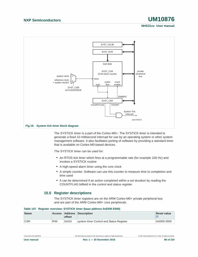
<Document ID>UM10876 All information provided in this document is subject to legal disclaimers. © NXP Semiconductors N.V. 2016. All rights reserved.
User manual Rev. 1 — 30 November 2016 98 of 234
NXP Semiconductors UM10876NHS31xx User manual
The SYSTICK timer is a part of the Cortex-M0+. The SYSTICK timer is intended to generate a fixed 10 millisecond interrupt for use by an operating system or other system management software. It also facilitates porting of software by providing a standard timer that is available on Cortex-M0-based devices.
The SYSTICK timer can be used for:
• An RTOS tick timer which fires at a programmable rate (for example 100 Hz) and invokes a SYSTICK routine
• A high-speed alarm timer using the core clock• A simple counter. Software can use this counter to measure time to completion and
time used• It can be determined if an action completed within a set duration by reading the
COUNTFLAG bitfield in the control and status register
15.5 Register descriptionsThe SYSTICK timer registers are on the ARM Cortex-M0+ private peripheral bus and are part of the ARM Cortex-M0+ core peripherals.
Fig 19. System tick timer block diagram
aaa-016413
SYST_CALIB
SYST_RVR
SYST_CSR
load data
clock
SYST_CSRbit CLKSOURCE
system clock
reference clock= system clock/2
1
0 under-flowload
ENABLE
System Tickinterrupt
TICKINTCOUNTFLAG
countenable
SYST_CVR24-bit down counter
privateperipheral
bus
Table 147. Register overview: SYSTICK timer (base address 0xE000 E000)Name Access Address
offsetDescription Reset value
[1]
CSR R/W 0x010 system timer Control and Status Register 0x0000 0000

<Document ID>UM10876 All information provided in this document is subject to legal disclaimers. © NXP Semiconductors N.V. 2016. All rights reserved.
User manual Rev. 1 — 30 November 2016 99 of 234
NXP Semiconductors UM10876NHS31xx User manual
[1] Reset Value reflects the data stored in used bits only. It does not include content of reserved bits.
15.5.1 System timer Control and Status Register (CSR)The CSR register contains control information for the SYSTICK timer and provides a status flag. This register is part of the ARM Cortex-M0+ core system timer register block.
This register determines the clock source for the system tick timer.
15.5.2 System Timer Reload value register (RVR)The RVR register is set to the value that is loaded into the SYSTICK timer whenever it counts down to zero. Timer initialization loads this register by software. If the CPU is running at the frequency intended for use with the CALIB value, the CALIB register may be read and used as the value for RVR register.
15.5.3 System Timer Current value register (CVR)The CVR register returns the current count from the System Tick counter.
RVR R/W 0x014 system timer Reload Value Register 0x0000 4E1F
CVR R/W 0x018 system timer Current Value Register 0x0000 0000
CALIB R/W 0x01C system timer Calibration value Register 0x0000 0004
Table 147. Register overview: SYSTICK timer (base address 0xE000 E000) _continued
Name Access Addressoffset
Description Reset value [1]
Table 148. CSR register (address 0xE000 E010) bit descriptionBit Symbol Description Reset value0 ENABLE enable System Tick counter. When logic1, the counter is enabled.
When logic 0, the counter is disabled0
1 TICKINT system Tick Interrupt enable. When logic 1, the System Tick interrupt is enabled. When logic 0, the System Tick interrupt is disabled. When enabled, the interrupt is generated when the System Tick counter counts down to 0
0
2 CLKSOURCE system tick Clock Source selection. When logic 1, the system clock (CPU) clock is selected. When logic 0, the system clock/2 is selected as the reference clock
0
15:3 - (reserved - do not write logic ones. The value read from a reserved bit is not defined)
-
16 COUNTFLAG returns 1 if the SYSTICK timer counted to logic 0 since the last read of this register
0
31:17 - (reserved - do not write logic ones. The value read from a reserved bit is not defined)
-
Table 149. RVR register (address 0xE000 E014) bit descriptionBit Symbol Description Reset value23:0 RELOAD this value that is loaded into the System Tick counter when it counts
down to 00xFFFFFF
31:24 - (reserved - do not write logic ones. The value read from a reserved bit is not defined)
-

<Document ID>UM10876 All information provided in this document is subject to legal disclaimers. © NXP Semiconductors N.V. 2016. All rights reserved.
User manual Rev. 1 — 30 November 2016 100 of 234
NXP Semiconductors UM10876NHS31xx User manual
15.5.4 System Timer Calibration value register (CALIB)The value of the SYSTCKCAL register in the system configuration block SYSCON (see Table 20) drives the value of the CALIB register.
15.6 Functional descriptionThe SYSTICK timer is a 24-bit timer that counts down to zero and generates an interrupt. The intent is to provide a fixed 10 millisecond time interval between interrupts. The SYSTICK timer is clocked from the CPU system clock (see Figure 19) or from the reference clock. The reference clock is fixed to half the frequency of the CPU clock. In order to generate recurring interrupts at a specific interval, the RVR register must be initialized with the correct value for the desired interval. A default value is provided in the CALIB register which is changeable by software.
If the CPU clock is set to 2 MHz, then this frequency gives a 10 millisecond interrupt rate.
15.6.1 Example timer calculationTo use the system tick timer, do the following:
1. Program the RVR register with the reload value RELOAD to obtain the desired time interval
2. Clear the CVR register by writing to it. This action ensures that the timer counts from the RVR value rather than an arbitrary value when the timer is enabled
3. Program the SCR register with the value 0x7 which enables the SYSTICK timer and the SYSTICK timer interrupt
The following example illustrates selecting the timer reload value to obtain a 10 ms time interval with the system clock set to 20 MHz.
Example (system clock = 50 MHz)The system tick clock = system clock = 8 MHz. Bit CLKSOURCE in the CSR register set to 1 (system clock).
Table 150. CVR register (address 0xE000 E018) bit descriptionBit Symbol Description Reset value23:0 CURRENT reading this register returns the current value of the
System Tick counter. Writing any value clears the System Tick counter and the COUNTFLAG bit in STCTRL
0xFFFFFF
31:24 - (reserved - do not write logic ones. The value read from a reserved bit is not defined)
-
Table 151. CALIB register (address 0xE000 E01C) bit descriptionBit Symbol Description Reset value23:0 TENMS 10 ms calibration value 0x4
29:24 - (reserved - do not write logic ones. The value read from a reserved bit is not defined)
-
30 SKEW if logical 1, the TENMS bit field is not accurate 0
31 NOREF if logical 1, it indicates that SYSTICK uses the core clock for counting as no external reference clock is available to be used
1’b0
<Document ID>UM10876 All information provided in this document is subject to legal disclaimers. © NXP Semiconductors N.V. 2016. All rights reserved.
User manual Rev. 1 — 30 November 2016 101 of 234
NXP Semiconductors UM10876NHS31xx User manual
RELOAD = (system tick clock frequency 10 ms) 1 = (8 MHz 10 ms) 1 = 80 000 1= 79 999 = 0x0001 387F.
<Document ID>UM10876 All information provided in this document is subject to legal disclaimers. © NXP Semiconductors N.V. 2016. All rights reserved.
User manual Rev. 1 — 30 November 2016 102 of 234
NXP Semiconductors UM10876NHS31xx User manual
16. 16-bit timer CT16B
16.1 About this chapterThis chapter describes the CT16B 16-bit timer, which is identical on all members of the NHS31xx family.
16.2 ConfigurationThe CT16B is configured as follows:
• Pins: The match outputs of the timer can be routed to I/O pins by setting the I/O pin function in the IOCON register. See Table 266.
• Clock: The PCLK clock clocks the CT16B block. This clock is derived from the system clock (see Figure 7). The clock can be enabled by setting bit 8 in the SYSAHBCLKCTRL register (see Table 14).
16.3 FeaturesOne 16-bit timer with a programmable 16-bit prescaler.
• Timer operation• Four 16-bit match registers that allow:
– Continuous operation with optional interrupt generation on match– Stop timer on match with optional interrupt generation– Reset timer on match with optional interrupt generation
• Up to two CT16B external outputs corresponding to the match registers with the following capabilities:– Set LOW on match– Set HIGH on match– Toggle on match– Do nothing on match
• Up to two match registers can be configured as PWM allowing the use of up to two match outputs as single edge controlled PWM outputs.
16.4 Applications
• Interval timer for generating internal events• Free-running timer• Pulse Width Modulator via match outputs
16.5 General descriptionThe timer is designed to count cycles of the peripheral clock (PCLK). It can optionally also generate interrupts or perform other actions at specified timer values based on four match registers. The peripheral clock is provided by the system clock (see Figure 7).

<Document ID>UM10876 All information provided in this document is subject to legal disclaimers. © NXP Semiconductors N.V. 2016. All rights reserved.
User manual Rev. 1 — 30 November 2016 103 of 234
NXP Semiconductors UM10876NHS31xx User manual
In PWM mode, four match registers can be used to provide a single-edge controlled PWM output on the match output pins. Use of the match registers that are not pinned out to control the PWM cycle length is recommended.
16.6 Pin descriptionTable 152 gives a brief summary of each of the timer-related pins.
16.7 Example timer operationFigure 20 shows a timer configured to reset the count and generate an interrupt on match. The prescaler is set to 2 and the match register set to 6. At the end of the timer cycle, where the match occurs, the timer count is reset giving a full length cycle to the match value. The match interrupt is generated in the next clock after the timer reached the match value.
Figure 21 shows a timer configured to stop and generate an interrupt on match. The prescaler is again set to 2 and the match register set to 6. The match interrupt is generated in the next clock after the timer reached the match value. The timer enable bit in TCR is cleared.
Table 152. Counter/timer pin descriptionPin Type DescriptionCT16B_M0 output 16-bit timer-match output 0
CT16B_M1 output 16-bit timer-match output 1
Fig 20. A timer cycle in which PR=2, MRx=6, and both interrupt and reset on match are enabled
aaa-017707
2 0 1 2 0 1 2 0 1 2 0 1
4
prescalecounter
timercounter 5 6 0 1
timer counterreset
interrupt
PCLK

<Document ID>UM10876 All information provided in this document is subject to legal disclaimers. © NXP Semiconductors N.V. 2016. All rights reserved.
User manual Rev. 1 — 30 November 2016 104 of 234
NXP Semiconductors UM10876NHS31xx User manual
Fig 21. A timer cycle in which PR=2, MRx=6, and both interrupt and stop on match are enabled
aaa-017709
2 0 1 2 0
1 0
4
prescalecounter
timercounter 5 6
TCR[0](counter enable)
interrupt
PCLK
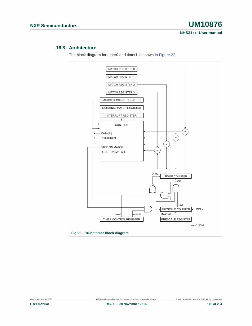
<Document ID>UM10876 All information provided in this document is subject to legal disclaimers. © NXP Semiconductors N.V. 2016. All rights reserved.
User manual Rev. 1 — 30 November 2016 105 of 234
NXP Semiconductors UM10876NHS31xx User manual
16.8 ArchitectureThe block diagram for timer0 and timer1 is shown in Figure 22.
Fig 22. 16-bit timer block diagram
aaa-016510
MATCH REGISTER 0
MATCH REGISTER 1
TIMER COUNTER
TCIPCLK
CE
CSN
PRESCALE COUNTER
PRESCALE REGISTER
enable MAXVALreset
TIMER CONTROL REGISTER
MATCH REGISTER 2
MATCH REGISTER 3
MATCH CONTROL REGISTER
EXTERNAL MATCH REGISTER
INTERRUPT REGISTER
CONTROL
MATn[2:]
STOP ON MATCH
RESET ON MATCH
INTERRUPT
=
=
=
=
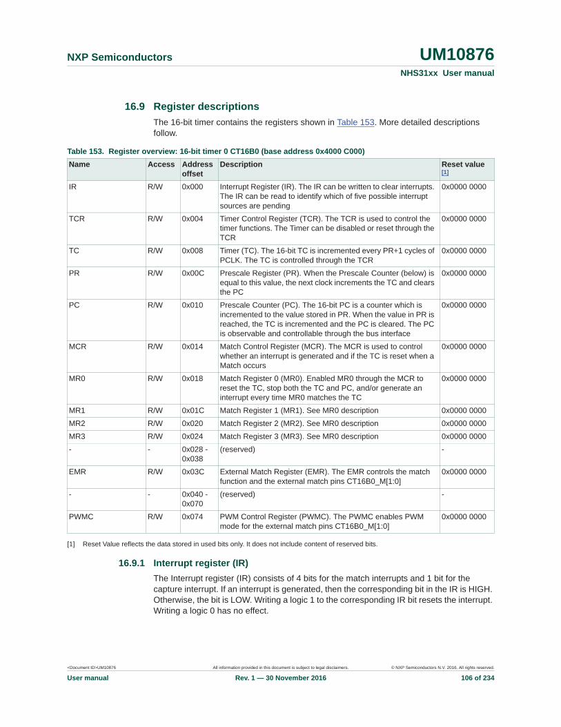
<Document ID>UM10876 All information provided in this document is subject to legal disclaimers. © NXP Semiconductors N.V. 2016. All rights reserved.
User manual Rev. 1 — 30 November 2016 106 of 234
NXP Semiconductors UM10876NHS31xx User manual
16.9 Register descriptionsThe 16-bit timer contains the registers shown in Table 153. More detailed descriptions follow.
[1] Reset Value reflects the data stored in used bits only. It does not include content of reserved bits.
16.9.1 Interrupt register (IR)The Interrupt register (IR) consists of 4 bits for the match interrupts and 1 bit for the capture interrupt. If an interrupt is generated, then the corresponding bit in the IR is HIGH. Otherwise, the bit is LOW. Writing a logic 1 to the corresponding IR bit resets the interrupt. Writing a logic 0 has no effect.
Table 153. Register overview: 16-bit timer 0 CT16B0 (base address 0x4000 C000)Name Access Address
offsetDescription Reset value
[1]
IR R/W 0x000 Interrupt Register (IR). The IR can be written to clear interrupts. The IR can be read to identify which of five possible interrupt sources are pending
0x0000 0000
TCR R/W 0x004 Timer Control Register (TCR). The TCR is used to control the timer functions. The Timer can be disabled or reset through the TCR
0x0000 0000
TC R/W 0x008 Timer (TC). The 16-bit TC is incremented every PR+1 cycles of PCLK. The TC is controlled through the TCR
0x0000 0000
PR R/W 0x00C Prescale Register (PR). When the Prescale Counter (below) is equal to this value, the next clock increments the TC and clears the PC
0x0000 0000
PC R/W 0x010 Prescale Counter (PC). The 16-bit PC is a counter which is incremented to the value stored in PR. When the value in PR is reached, the TC is incremented and the PC is cleared. The PC is observable and controllable through the bus interface
0x0000 0000
MCR R/W 0x014 Match Control Register (MCR). The MCR is used to control whether an interrupt is generated and if the TC is reset when a Match occurs
0x0000 0000
MR0 R/W 0x018 Match Register 0 (MR0). Enabled MR0 through the MCR to reset the TC, stop both the TC and PC, and/or generate an interrupt every time MR0 matches the TC
0x0000 0000
MR1 R/W 0x01C Match Register 1 (MR1). See MR0 description 0x0000 0000
MR2 R/W 0x020 Match Register 2 (MR2). See MR0 description 0x0000 0000
MR3 R/W 0x024 Match Register 3 (MR3). See MR0 description 0x0000 0000
- - 0x028 -0x038
(reserved) -
EMR R/W 0x03C External Match Register (EMR). The EMR controls the match function and the external match pins CT16B0_M[1:0]
0x0000 0000
- - 0x040 -0x070
(reserved) -
PWMC R/W 0x074 PWM Control Register (PWMC). The PWMC enables PWM mode for the external match pins CT16B0_M[1:0]
0x0000 0000
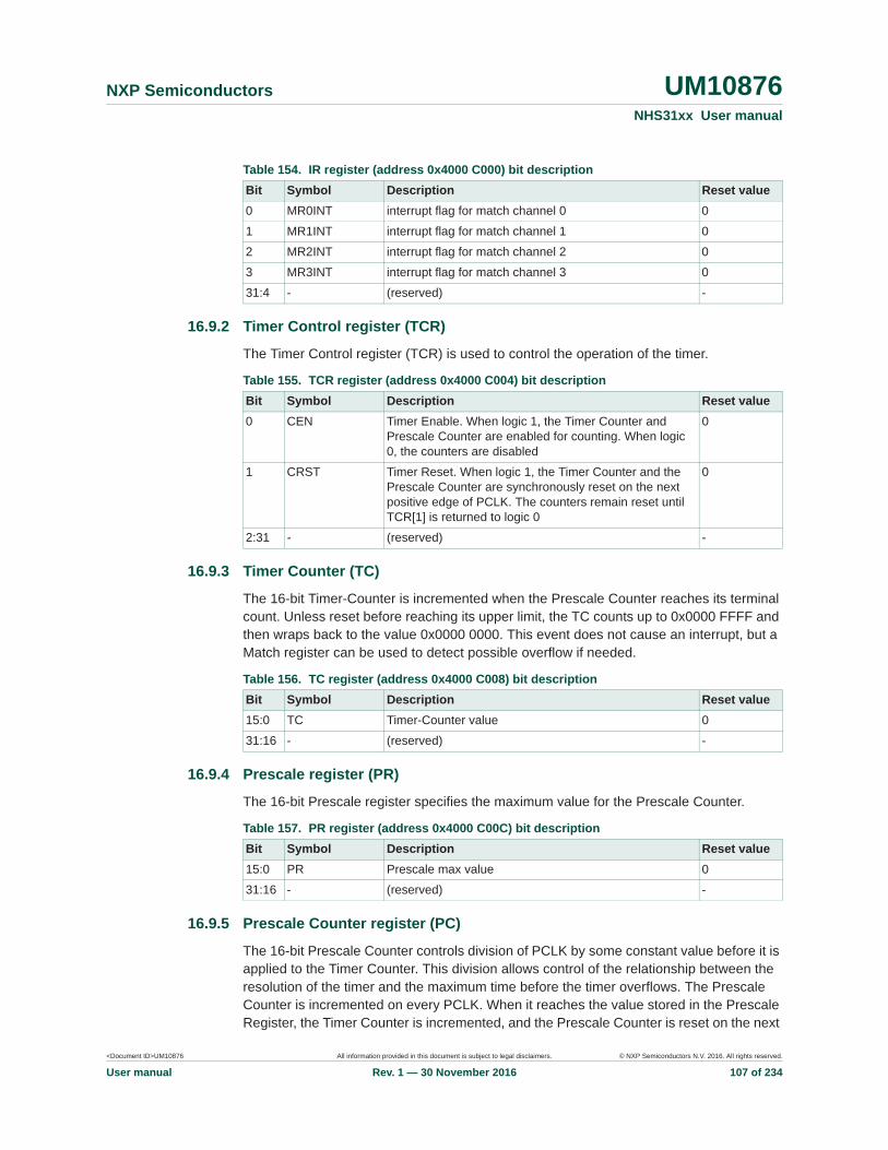
<Document ID>UM10876 All information provided in this document is subject to legal disclaimers. © NXP Semiconductors N.V. 2016. All rights reserved.
User manual Rev. 1 — 30 November 2016 107 of 234
NXP Semiconductors UM10876NHS31xx User manual
16.9.2 Timer Control register (TCR)
The Timer Control register (TCR) is used to control the operation of the timer.
16.9.3 Timer Counter (TC)
The 16-bit Timer-Counter is incremented when the Prescale Counter reaches its terminal count. Unless reset before reaching its upper limit, the TC counts up to 0x0000 FFFF and then wraps back to the value 0x0000 0000. This event does not cause an interrupt, but a Match register can be used to detect possible overflow if needed.
16.9.4 Prescale register (PR)
The 16-bit Prescale register specifies the maximum value for the Prescale Counter.
16.9.5 Prescale Counter register (PC)
The 16-bit Prescale Counter controls division of PCLK by some constant value before it is applied to the Timer Counter. This division allows control of the relationship between the resolution of the timer and the maximum time before the timer overflows. The Prescale Counter is incremented on every PCLK. When it reaches the value stored in the Prescale Register, the Timer Counter is incremented, and the Prescale Counter is reset on the next
Table 154. IR register (address 0x4000 C000) bit descriptionBit Symbol Description Reset value0 MR0INT interrupt flag for match channel 0 0
1 MR1INT interrupt flag for match channel 1 0
2 MR2INT interrupt flag for match channel 2 0
3 MR3INT interrupt flag for match channel 3 0
31:4 - (reserved) -
Table 155. TCR register (address 0x4000 C004) bit descriptionBit Symbol Description Reset value0 CEN Timer Enable. When logic 1, the Timer Counter and
Prescale Counter are enabled for counting. When logic 0, the counters are disabled
0
1 CRST Timer Reset. When logic 1, the Timer Counter and the Prescale Counter are synchronously reset on the next positive edge of PCLK. The counters remain reset until TCR[1] is returned to logic 0
0
2:31 - (reserved) -
Table 156. TC register (address 0x4000 C008) bit descriptionBit Symbol Description Reset value15:0 TC Timer-Counter value 0
31:16 - (reserved) -
Table 157. PR register (address 0x4000 C00C) bit descriptionBit Symbol Description Reset value15:0 PR Prescale max value 0
31:16 - (reserved) -
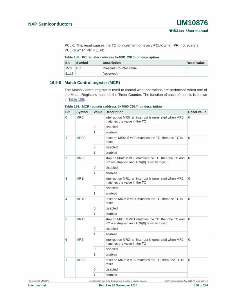
<Document ID>UM10876 All information provided in this document is subject to legal disclaimers. © NXP Semiconductors N.V. 2016. All rights reserved.
User manual Rev. 1 — 30 November 2016 108 of 234
NXP Semiconductors UM10876NHS31xx User manual
PCLK. This reset causes the TC to increment on every PCLK when PR = 0, every 2 PCLKs when PR = 1, etc.
16.9.6 Match Control register (MCR)
The Match Control register is used to control what operations are performed when one of the Match Registers matches the Timer Counter. The function of each of the bits is shown in Table 159.
Table 158. PC register (address 0x4001 C010) bit descriptionBit Symbol Description Reset value15:0 PC Prescale Counter value 0
31:16 - (reserved) -
Table 159. MCR register (address 0x4000 C014) bit descriptionBit Symbol Value Description Reset value0 MR0I interrupt on MR0: an interrupt is generated when MR0
matches the value in the TC0
0 disabled
1 enabled
1 MR0R reset on MR0: If MR0 matches the TC, then the TC is reset
0
0 disabled
1 enabled
2 MR0S stop on MR0: If MR0 matches the TC, then the TC and PC are stopped and TCR[0] is set to logic 0
0
0 disabled
1 enabled
3 MR1I interrupt on MR1: an interrupt is generated when MR1 matches the value in the TC
0
0 disabled
1 enabled
4 MR1R reset on MR1: If MR1 matches the TC, then the TC is reset
0
0 disabled
1 enabled
5 MR1S stop on MR1: If MR1 matches the TC, then the TC and PC are stopped and TCR[0] is set to logic 0
0
0 disabled
1 enabled
6 MR2I interrupt on MR2: an interrupt is generated when MR2 matches the value in the TC
0
0 disabled
1 enabled
7 MR2R reset on MR2: If MR2 matches the TC, then, the TC is reset
0
0 disabled
1 enabled
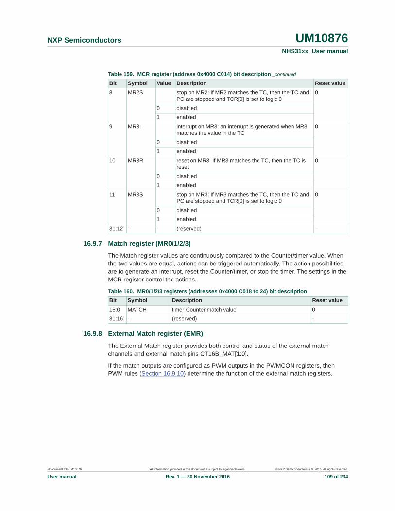
<Document ID>UM10876 All information provided in this document is subject to legal disclaimers. © NXP Semiconductors N.V. 2016. All rights reserved.
User manual Rev. 1 — 30 November 2016 109 of 234
NXP Semiconductors UM10876NHS31xx User manual
16.9.7 Match register (MR0/1/2/3)
The Match register values are continuously compared to the Counter/timer value. When the two values are equal, actions can be triggered automatically. The action possibilities are to generate an interrupt, reset the Counter/timer, or stop the timer. The settings in the MCR register control the actions.
16.9.8 External Match register (EMR)
The External Match register provides both control and status of the external match channels and external match pins CT16B_MAT[1:0].
If the match outputs are configured as PWM outputs in the PWMCON registers, then PWM rules (Section 16.9.10) determine the function of the external match registers.
8 MR2S stop on MR2: If MR2 matches the TC, then the TC and PC are stopped and TCR[0] is set to logic 0
0
0 disabled
1 enabled
9 MR3I interrupt on MR3: an interrupt is generated when MR3 matches the value in the TC
0
0 disabled
1 enabled
10 MR3R reset on MR3: If MR3 matches the TC, then the TC is reset
0
0 disabled
1 enabled
11 MR3S stop on MR3: If MR3 matches the TC, then the TC and PC are stopped and TCR[0] is set to logic 0
0
0 disabled
1 enabled
31:12 - - (reserved) -
Table 159. MCR register (address 0x4000 C014) bit description _continued
Bit Symbol Value Description Reset value
Table 160. MR0/1/2/3 registers (addresses 0x4000 C018 to 24) bit descriptionBit Symbol Description Reset value15:0 MATCH timer-Counter match value 0
31:16 - (reserved) -
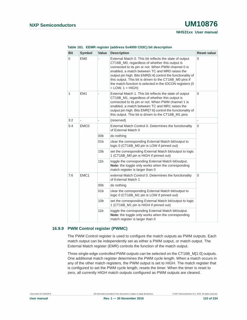
<Document ID>UM10876 All information provided in this document is subject to legal disclaimers. © NXP Semiconductors N.V. 2016. All rights reserved.
User manual Rev. 1 — 30 November 2016 110 of 234
NXP Semiconductors UM10876NHS31xx User manual
16.9.9 PWM Control register (PWMC)
The PWM Control register is used to configure the match outputs as PWM outputs. Each match output can be independently set as either a PWM output, or match output. The External Match register (EMR) controls the function of the match output.
Three single-edge controlled PWM outputs can be selected on the CT16B_M[1:0] outputs. One additional match register determines the PWM cycle length. When a match occurs in any of the other match registers, the PWM output is set to HIGH. The match register that is configured to set the PWM cycle length, resets the timer. When the timer is reset to zero, all currently HIGH match outputs configured as PWM outputs are cleared.
Table 161. EEMR register (address 0x4000 C03C) bit descriptionBit Symbol Value Description Reset value0 EM0 - External Match 0. This bit reflects the state of output
CT16B_M0, regardless of whether this output is connected to its pin or not. When PWM channel 0 is enabled, a match between TC and MR0 raises the output pin high. Bits EMR[5:4] control the functionality of this output. This bit is driven to the CT16B_M0 pins if the match function is selected in the IOCON registers (0 = LOW, 1 = HIGH)
0
1 EM1 - External Match 1. This bit reflects the state of output CT16B_M1, regardless of whether this output is connected to its pin or not. When PWM channel 1 is enabled, a match between TC and MR1 raises the output pin high. Bits EMR[7:6] control the functionality of this output. This bit is driven to the CT16B_M1 pins
0
3:2 - - (reserved) -
5:4 EMC0 External Match Control 0. Determines the functionality of External Match 0
0
00b do nothing
01b clear the corresponding External Match bit/output to logic 0 (CT16B_M0 pin is LOW if pinned out)
10b set the corresponding External Match bit/output to logic 1 (CT16B_M0 pin is HIGH if pinned out)
11b toggle the corresponding External Match bit/output. Note: the toggle only works when the corresponding match register is larger than 0
7:6 EMC1 external Match Control 0. Determines the functionality of External Match 1
0
00b do nothing
01b clear the corresponding External Match bit/output to logic 0 (CT16B_M1 pin is LOW if pinned out)
10b set the corresponding External Match bit/output to logic 1 (CT16B_M1 pin is HIGH if pinned out)
11b toggle the corresponding External Match bit/output. Note: the toggle only works when the corresponding match register is larger than 0

<Document ID>UM10876 All information provided in this document is subject to legal disclaimers. © NXP Semiconductors N.V. 2016. All rights reserved.
User manual Rev. 1 — 30 November 2016 111 of 234
NXP Semiconductors UM10876NHS31xx User manual
16.9.10 Rules for single edge controlled PWM outputs
1. All single edge controlled PWM outputs go LOW at the beginning of each PWM cycle unless their match value is equal to zero
2. Each PWM output goes HIGH when its match value is reached. If no match occurs (i.e. the match value is greater than the PWM cycle length), the PWM output remains continuously LOW
3. If a match value larger than the PWM cycle length is written to the match register, and the PWM signal is HIGH already, the PWM signal is cleared on the start of the next PWM cycle
4. If a match register value equals the timer reset value, then the PWM output will be reset to LOW on the next clock tick. Therefore, the PWM output always consists of a one clock tick wide positive pulse. The PWM cycle length is the same as the timer reset value
5. If a match register is set to zero, then the PWM output goes HIGH the first time the timer goes back to zero and remains HIGH
Note: When the match outputs are used as PWM outputs, the reset and stop bits in the Match Control Register (MCR) must be set to logic 0, except for the match register. The match register sets the PWM cycle length. For this register, set the MRR bit to logic 1 to enable the timer reset when the timer value matches the value of the corresponding match register.
Table 162. PWMC register (address 0x4000 C074) bit descriptionBit Symbol Value Description Reset value0 PWMEN0 PWM channel0 enable 0
0 EM0 controls the CT16B_M0
1 PWM mode is enabled for CT16B_M0
1 PWMEN1 PWM channel1 enable 0
0 EM1 controls the CT16B0_M1
1 PWM mode is enabled for CT16B_M1
31:2 - - (reserved) -
Fig 23. Sample PWM waveforms with a PWM cycle length of 100 (selected by MR2) and MAT2:0 enabled as PWM outputs by the PWCM register.
aaa-016509
PWM0/MAT0
PWM1/MAT1
PWM2/MAT2
MR0 = 65
(counter is reset)
0 41 65 100
MR1 = 41
MR2 = 100

<Document ID>UM10876 All information provided in this document is subject to legal disclaimers. © NXP Semiconductors N.V. 2016. All rights reserved.
User manual Rev. 1 — 30 November 2016 112 of 234
NXP Semiconductors UM10876NHS31xx User manual
17. 32-bit timer CT32B
17.1 About this chapterThis chapter describes the CT32B 32-bit timer, which is identical on all members of the NHS31xx family.
17.2 ConfigurationThe CT32B is configured as follows:
• Pins: The match outputs of the timer can be routed to I/O pins by setting the I/O pin function in the IOCON register. See Table 266.
• Clock: The PCLK clock clocks the CT32B block. This clock is derived from the system clock(see Figure 7). The clock can be enabled by setting bit 8 in the SYSAHBCLKCTRL register (see Table 14).
17.3 FeaturesOne 32-bit timer with a programmable 32-bit prescaler.
• Timer operation• Four 32-bit match registers that allow:
– Continuous operation with optional interrupt generation on match– Stop timer on match with optional interrupt generation– Reset timer on match with optional interrupt generation
• Up to two CT32B external outputs corresponding to the match registers with the following capabilities:– Set LOW on match– Set HIGH on match– Toggle on match– Do nothing on match
• Up to two match registers can be configured as PWM allowing the use of up to two match outputs as single edge controlled PWM outputs.
17.4 Applications
• Interval timer for generating internal events• Free-running timer• Pulse Width Modulator via match outputs
17.5 General descriptionThe timer is designed to count cycles of the peripheral clock (PCLK). It can optionally also generate interrupts or perform other actions at specified timer values based on four match registers. The peripheral clock is provided by the system clock (see Figure 7).
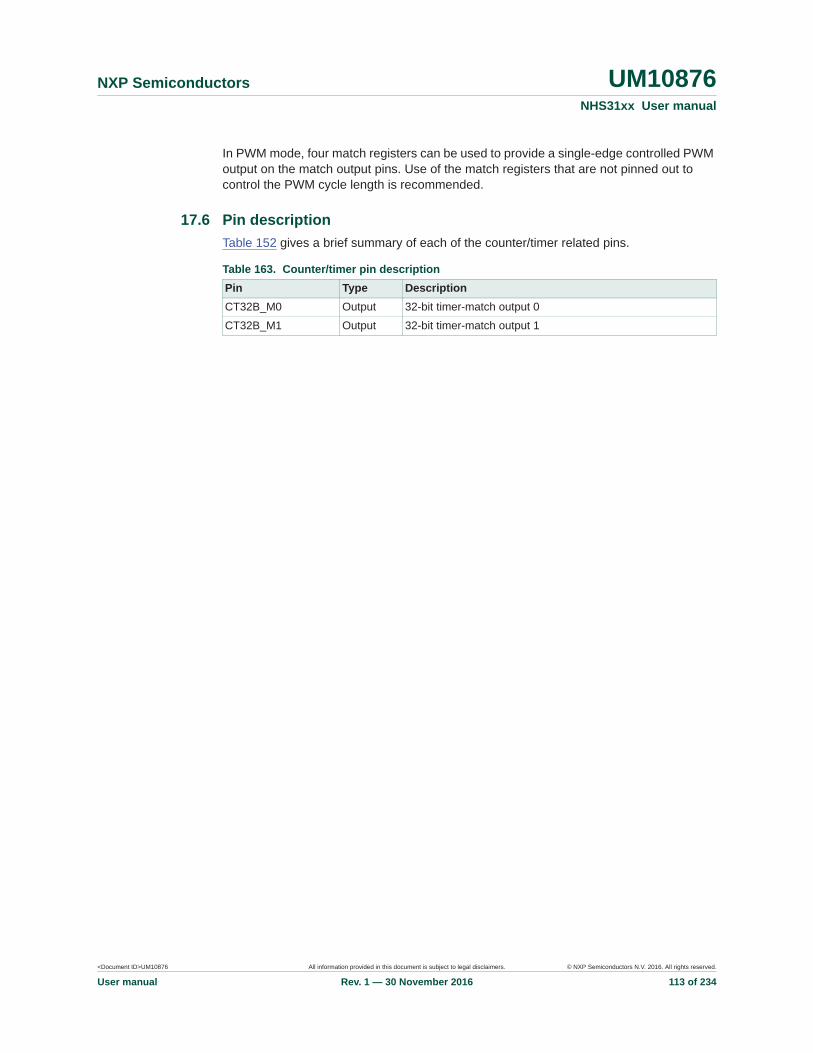
<Document ID>UM10876 All information provided in this document is subject to legal disclaimers. © NXP Semiconductors N.V. 2016. All rights reserved.
User manual Rev. 1 — 30 November 2016 113 of 234
NXP Semiconductors UM10876NHS31xx User manual
In PWM mode, four match registers can be used to provide a single-edge controlled PWM output on the match output pins. Use of the match registers that are not pinned out to control the PWM cycle length is recommended.
17.6 Pin descriptionTable 152 gives a brief summary of each of the counter/timer related pins.
Table 163. Counter/timer pin descriptionPin Type DescriptionCT32B_M0 Output 32-bit timer-match output 0
CT32B_M1 Output 32-bit timer-match output 1

<Document ID>UM10876 All information provided in this document is subject to legal disclaimers. © NXP Semiconductors N.V. 2016. All rights reserved.
User manual Rev. 1 — 30 November 2016 114 of 234
NXP Semiconductors UM10876NHS31xx User manual
17.7 Example timer operationFigure 20 shows a timer configured to reset the count and generate an interrupt on match. The prescaler is set to 2 and the match register set to 6. At the end of the timer cycle, where the match occurs, the timer count is reset giving a full length cycle to the match value. The match interrupt is generated in the next clock after the timer reached the match value.
Figure 21 shows a timer configured to stop and generate an interrupt on match. The prescaler is again set to 2 and the match register set to 6. The match interrupt is generated in the next clock after the timer reached the match value. The timer enable bit in TCR is cleared.
Fig 24. A timer cycle in which PR=2, MRx=6, and both interrupt and reset on match are enabled
aaa-017707
2 0 1 2 0 1 2 0 1 2 0 1
4
prescalecounter
timercounter 5 6 0 1
timer counterreset
interrupt
PCLK
Fig 25. A timer cycle in which PR=2, MRx=6, and both interrupt and stop on match are enabled
aaa-017709
2 0 1 2 0
1 0
4
prescalecounter
timercounter 5 6
TCR[0](counter enable)
interrupt
PCLK

<Document ID>UM10876 All information provided in this document is subject to legal disclaimers. © NXP Semiconductors N.V. 2016. All rights reserved.
User manual Rev. 1 — 30 November 2016 115 of 234
NXP Semiconductors UM10876NHS31xx User manual
17.8 ArchitectureThe block diagram for counter/timer0 and counter/timer1 is shown in Figure 22.
Fig 26. 32-bit counter/timer block diagram
aaa-016510
MATCH REGISTER 0
MATCH REGISTER 1
TIMER COUNTER
TCIPCLK
CE
CSN
PRESCALE COUNTER
PRESCALE REGISTER
enable MAXVALreset
TIMER CONTROL REGISTER
MATCH REGISTER 2
MATCH REGISTER 3
MATCH CONTROL REGISTER
EXTERNAL MATCH REGISTER
INTERRUPT REGISTER
CONTROL
MATn[2:]
STOP ON MATCH
RESET ON MATCH
INTERRUPT
=
=
=
=

<Document ID>UM10876 All information provided in this document is subject to legal disclaimers. © NXP Semiconductors N.V. 2016. All rights reserved.
User manual Rev. 1 — 30 November 2016 116 of 234
NXP Semiconductors UM10876NHS31xx User manual
17.9 Register descriptionsThe 32-bit counter/timer contains the registers shown in Table 164. More detailed descriptions follow.
[1] Reset Value reflects the data stored in used bits only. It does not include content of reserved bits.
17.9.1 Interrupt register (IR)The Interrupt register (IR) consists of 4 bits for the match interrupts and 1 bit for the capture interrupt. If an interrupt is generated, then the corresponding bit in the IR is HIGH. Otherwise, the bit is LOW. Writing a logic 1 to the corresponding IR bit resets the interrupt. Writing a logic 0 has no effect.
Table 164. Register overview: 32-bit counter/timer 0 CT32B (base address 0x4000 4000)Name Access Address
offsetDescription Reset value
[1]
IR R/W 0x000 Interrupt Register (IR). The IR can be written to clear interrupts. The IR can be read to identify which of five possible interrupt sources are pending
0x0000 0000
TCR R/W 0x004 Timer Control Register (TCR). The TCR is used to control the Timer Counter functions. The Timer Counter can be disabled or reset through the TCR
0x0000 0000
TC R/W 0x008 Timer Counter (TC). The 32-bit TC is incremented every PR+1 cycles of PCLK. The TC is controlled through the TCR
0x0000 0000
PR R/W 0x00C Prescale Register (PR). When the Prescale Counter (below) is equal to this value, the next clock increments the TC and clears the PC
0x0000 0000
PC R/W 0x010 Prescale Counter (PC). The 32-bit PC is a counter which is incremented to the value stored in PR. When the value in PR is reached, the TC is incriminated and the PC is cleared. The PC is observable and controllable through the bus interface
0x0000 0000
MCR R/W 0x014 Match Control Register (MCR). The MCR is used to control whether an interrupt is generated and if the TC is reset when a Match occurs
0x0000 0000
MR0 R/W 0x018 Match Register 0 (MR0). Enabled MR0 through the MCR to reset the TC, stop both the TC and PC, and/or generate an interrupt every time MR0 matches the TC
0x0000 0000
MR1 R/W 0x01C Match Register 1 (MR1). See MR0 description 0x0000 0000
MR2 R/W 0x020 Match Register 2 (MR2). See MR0 description 0x0000 0000
MR3 R/W 0x024 Match Register 3 (MR3). See MR0 description 0x0000 0000
- R/W 0x028 -0x038
(reserved) -
EMR R/W 0x03C External Match Register (EMR). The EMR controls the match function and the external match pins CT326B_M[1:0]
0x0000 0000
- - 0x040 -0x070
(reserved) -
PWMC R/W 0x074 PWM Control Register (PWMC). The PWMC enables PWM mode for the external match pins CT32B_M[1:0]
0x0000 0000

<Document ID>UM10876 All information provided in this document is subject to legal disclaimers. © NXP Semiconductors N.V. 2016. All rights reserved.
User manual Rev. 1 — 30 November 2016 117 of 234
NXP Semiconductors UM10876NHS31xx User manual
17.9.2 Timer Control register (TCR)
The Timer Control register (TCR) is used to control the operation of the counter/timer.
17.9.3 Timer Counter register (TC)
The 32-bit Timer-Counter is incremented when the Prescale Counter reaches its terminal count. Unless reset before reaching its upper limit, the TC counts up to 0xFFFF FFFF and then wraps back to the value 0x0000 0000. This event does not cause an interrupt, but a Match register can be used to detect possible overflow if needed.
17.9.4 Prescale register (PR)
The 32-bit Prescale register specifies the maximum value for the Prescale Counter.
17.9.5 Prescale Counter register (PC)
The 32-bit Prescale Counter controls division of PCLK by some constant value before it is applied to the Timer Counter. This division allows control of the relationship between the resolution of the timer and the maximum time before the timer overflows. The Prescale Counter is incremented on every PCLK. When it reaches the value stored in the Prescale Register, the Timer Counter is incremented, and the Prescale Counter is reset on the next PCLK. This reset causes the TC to increment on every PCLK when PR = 0, every
Table 165. IR register (address 0x4000 4000) bit descriptionBit Symbol Description Reset value0 MR0INT interrupt flag for match channel 0 0x0000 0000
1 MR1INT interrupt flag for match channel 1 0x0000 0000
2 MR2INT interrupt flag for match channel 2 0x0000 0000
3 MR3INT interrupt flag for match channel 3 0x0000 0000
31:4 - (reserved) -
Table 166. TCR register (address 0x4000 4004) bit descriptionBit Symbol Description Reset value0 CEN Counter Enable. When one, the Timer Counter and
Prescale Counter are enabled for counting. When zero, the counters are disabled
0
1 CRST Counter Reset. When one, the Timer Counter and the Prescale Counter are synchronously reset on the next positive edge of PCLK. The counters remain reset until TCR[1] is returned to zero
0
31:2 - (reserved) -
Table 167. TC register (address 0x4000 4008) bit descriptionBit Symbol Description Reset value15:0 TC Timer Counter value 0
31:16 - (reserved) -
Table 168. PR register (address 0x4000 400C) bit descriptionBit Symbol Description Reset value31:0 PR Prescale max value 0

<Document ID>UM10876 All information provided in this document is subject to legal disclaimers. © NXP Semiconductors N.V. 2016. All rights reserved.
User manual Rev. 1 — 30 November 2016 118 of 234
NXP Semiconductors UM10876NHS31xx User manual
2 PCLKs when PR = 1, etc.
17.9.6 Match Control register (MCR)
The Match Control register is used to control what operations are performed when one of the Match Registers matches the Timer Counter. The function of each of the bits is shown in Table 170.
Table 169. PC register (address 0x4001 4010) bit descriptionBit Symbol Description Reset value31:0 PC Prescale counter value 0
Table 170. MCR register (address 0x4000 4014) bit descriptionBit Symbol Value Description Reset value0 MR0I interrupt on MR0: an interrupt is generated when MR0
matches the value in the TC0
0 disabled
1 enabled
1 MR0R reset on MR0: If MR0 matches the TC, then the TC is reset
0
0 disabled
1 enabled
2 MR0S if MR0 matches the TC, then the TC and PC are stopped and TCR[0] is set to logic 0
0
0 disabled
1 enabled
3 MR1I interrupt on MR1: an interrupt is generated when MR1 matches the value in the TC
0
0 disabled
1 enabled
4 MR1R reset on MR1: If MR1 matches the TC, then the TC is reset
0
0 disabled
1 enabled
5 MR1S stop on MR1: If MR1 matches the TC, then the TC and PC are stopped and TCR[0] is set to logic 0
0
0 disabled
1 enabled
6 MR2I interrupt on MR2: an interrupt is generated when MR2 matches the value in the TC
0
0 disabled
1 enabled
7 MR2R reset on MR2: If MR2 matches the TC, then, the TC is reset
0
0 disabled
1 enabled
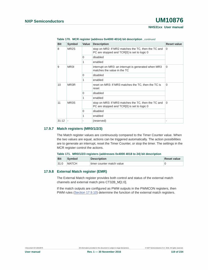
<Document ID>UM10876 All information provided in this document is subject to legal disclaimers. © NXP Semiconductors N.V. 2016. All rights reserved.
User manual Rev. 1 — 30 November 2016 119 of 234
NXP Semiconductors UM10876NHS31xx User manual
17.9.7 Match registers (MR0/1/2/3)
The Match register values are continuously compared to the Timer Counter value. When the two values are equal, actions can be triggered automatically. The action possibilities are to generate an interrupt, reset the Timer Counter, or stop the timer. The settings in the MCR register control the actions.
17.9.8 External Match register (EMR)
The External Match register provides both control and status of the external match channels and external match pins CT32B_M[1:0].
If the match outputs are configured as PWM outputs in the PWMCON registers, then PWM rules (Section 17.9.10) determine the function of the external match registers.
8 MR2S stop on MR2: If MR2 matches the TC, then the TC and PC are stopped and TCR[0] is set to logic 0
0
0 disabled
1 enabled
9 MR3I interrupt on MR3: an interrupt is generated when MR3 matches the value in the TC
0
0 disabled
1 enabled
10 MR3R reset on MR3: If MR3 matches the TC, then the TC is reset
0
0 disabled
1 enabled
11 MR3S stop on MR3: If MR3 matches the TC, then the TC and PC are stopped and TCR[0] is set to logic 0
0
0 disabled
1 enabled
31:12 - - (reserved) -
Table 170. MCR register (address 0x4000 4014) bit description _continued
Bit Symbol Value Description Reset value
Table 171. MR0/1/2/3 registers (addresses 0x4000 4018 to 24) bit descriptionBit Symbol Description Reset value31:0 MATCH timer counter match value 0

<Document ID>UM10876 All information provided in this document is subject to legal disclaimers. © NXP Semiconductors N.V. 2016. All rights reserved.
User manual Rev. 1 — 30 November 2016 120 of 234
NXP Semiconductors UM10876NHS31xx User manual
17.9.9 PWM Control register (PWMC)
The PWM Control register is used to configure the match outputs as PWM outputs. Each match output can be independently set as either a PWM output, or match output. The External Match register (EMR) controls the function of the match output.
Three single-edge controlled PWM outputs can be selected on the CT32B_M[1:0] outputs. One additional match register determines the PWM cycle length. When a match occurs in any of the other match registers, the PWM output is set to HIGH. The match register that is configured to set the PWM cycle length, resets the timer. When the timer is reset to zero, all currently HIGH match outputs configured as PWM outputs are cleared.
Table 172. EMR register (address 0x4000 403C) bit descriptionBit Symbol Value Description Reset value0 EM0 - External Match 0. This bit reflects the state of output
CT32B_M0, regardless of whether this output is connected to its pin. When a match occurs between the TC and MR0, this bit can either toggle, go LOW, go HIGH, or do nothing. Bits EMR[5:4] control the functionality of this output. This bit is driven to the CT32B_M0 pins if the match function is selected in the IOCON registers (0 = LOW, 1 = HIGH)
0
1 EM1 - External Match 1. This bit reflects the state of output CT32B_M1, regardless of whether this output is connected to its pin. When a match occurs between the TC and MR1, this bit can either toggle, go LOW, go HIGH, or do nothing. Bits EMR[7:6] control the functionality of this output. This bit is driven to the CT32B_M1 pins
0
3:2 - - (reserved) -
5:4 EMC0 External Match Control 0. determines the functionality of External Match 0
0
00b do nothing
01b clear the corresponding External Match bit/output to logic 0 (CT32B_M0 pin is LOW if pinned out)
10b set the corresponding External Match bit/output to logic 1 (CT326B_M0 pin is HIGH if pinned out)
11b toggle the corresponding External Match bit/output. Note: the toggle only works when the corresponding match register is larger than 0
7:6 EMC1 External Match Control 1. Determines the functionality of External Match 1
0
00b do nothing
01b clear the corresponding External Match bit/output to logic 0 (CT32B_M1 pin is LOW if pinned out)
10b set the corresponding External Match bit/output to logic 1 (CT326B_M1 pin is HIGH if pinned out)
11b toggle the corresponding External Match bit/output. Note: the toggle only works when the corresponding match register is larger than 0

<Document ID>UM10876 All information provided in this document is subject to legal disclaimers. © NXP Semiconductors N.V. 2016. All rights reserved.
User manual Rev. 1 — 30 November 2016 121 of 234
NXP Semiconductors UM10876NHS31xx User manual
17.9.10 Rules for single edge controlled PWM outputs
1. All single edge controlled PWM outputs go LOW at the beginning of each PWM cycle unless their match value is equal to zero
2. Each PWM output goes HIGH when its match value is reached. If no match occurs (i.e. the match value is greater than the PWM cycle length), the PWM output remains continuously LOW
3. If a match value larger than the PWM cycle length is written to the match register, and the PWM signal is HIGH already, the PWM signal is cleared on the start of the next PWM cycle
4. If a match register value equals the timer reset value, then the PWM output will be reset to LOW on the next clock tick. Therefore, the PWM output always consists of a one clock tick wide positive pulse. The PWM cycle length is the same as the timer reset value
5. If a match register is set to zero, then the PWM output goes HIGH the first time the timer goes back to zero and remains HIGH
Note: When the match outputs are used as PWM outputs, the reset and stop bits in the Match Control Register (MCR) must be set to logic 0, except for the match register. The match register sets the PWM cycle length. For this register, set the MRR bit to logic 1 to enable the timer reset when the timer value matches the value of the corresponding match register.
Table 173. PWMC register (address 0x4000 4074) bit descriptionBit Symbol Value Description Reset value0 PWMEN0 PWM channel0 enable 0
0 EM0 controls the CT32B_M0
1 PWM mode is enabled for CT32B_M0
1 PWMEN1 PWM channel1 enable 0
0 EM1 controls the CT32B0_M1
1 PWM mode is enabled for CT32B_M1
31:2 - - (reserved) -
Fig 27. Sample PWM waveforms with a PWM cycle length of 100 (selected by MR2) and MAT2:0 enabled as PWM outputs by the PWCM register.
aaa-016509
PWM0/MAT0
PWM1/MAT1
PWM2/MAT2
MR0 = 65
(counter is reset)
0 41 65 100
MR1 = 41
MR2 = 100
<Document ID>UM10876 All information provided in this document is subject to legal disclaimers. © NXP Semiconductors N.V. 2016. All rights reserved.
User manual Rev. 1 — 30 November 2016 122 of 234
NXP Semiconductors UM10876NHS31xx User manual
18. EEPROM controller
18.1 About this chapterThis chapter provides an overview of the EEPROM control and interface.
18.2 On-chip EEPROMThe NHS31xx contains a 4 kB EEPROM. This EEPROM is organized in 64 rows of32 16-bit words. Of these rows, the last four contain calibration and test data and are locked. This data is either used by the boot loader after reset, or made accessible to the application via firmware Application Programming Interface (API).
18.3 Functional description
18.3.1 Reading from EEPROMReading is done via the AHB interface. The memory is mapped on the bus address space as a contiguous address space. Memory data words are seen on the bus using a little endian arrangement: Bits in the memory word are split in bytes so that byte 0 is made of bits 7:0, byte 1 by bits 15:8, and so on. Word 0, byte 0 is at byte address 0 in the bus, followed by word 0, byte 1, and so on, until word 0 is completed. The next address refers to word 1, byte 0, and so on.
The bus data width may have the same size as the memory data word, or be wider, or smaller. Additionally, on an AHB, it is possible to perform reads of a size which is smaller than the bus size.
If a read transfer request is detected, one or more memory read operations are performed sequentially until the required data is made available.
In the case of multiple memory read operations to satisfy a single bus read request, the order in which operations are performed is unspecified. Therefore, all status bits which refer to the ’latest memory read’ are related to just one of the many read operations performed. To identify precisely which status applies to which word, use a read size which matches the memory data size. Conversely, flags refer to the full word even if only part of a memory word is read.
If the memory is busy with writes or other reads when a read request is placed on the bus, additional wait states are inserted until the requested read can be started. This action may be because, for instance, the memory is busy due to initialization or signature calculation.
If the memory is busy doing a program/erase when a read request is placed on the bus, an error response is given on the bus.
18.3.2 Writing to EEPROMErasing and programming is performed, as a single operation, on one or more words inside a single page.
Previous write operations have transferred the data to be programmed into the memory page buffer. The page buffer tracks which words were written to (offset within the page only). Words not written to, retain their previous content.
<Document ID>UM10876 All information provided in this document is subject to legal disclaimers. © NXP Semiconductors N.V. 2016. All rights reserved.
User manual Rev. 1 — 30 November 2016 123 of 234
NXP Semiconductors UM10876NHS31xx User manual
Note: Do not write more than once on a position within a page register with different data, otherwise data loss may occur.
When writing the binary value 110b inside the CMD register field, programming starts: the page specified in the last write operation is updated with the content of the page buffer, and the page buffer is cleared.
Note: It is the act of writing 110b in CMD that starts programming, it is irrelevant whether CMD already contained 110b from a previous programming operation.
If another program/erase is in progress while the CMD register is written, the control interface returns an error. If any other memory operation is in progress, wait states are added until the memory is available.
The EEPAUTOPROG register allows an additional way of starting EEPROM programming:
• If EEPAUTOPROG contains the value 01b, then EEPROM programming is also started after each successful write interface transaction.
• If EEPAUTOPROG contains the value 10b, then EEPROM programming is started after each successful write interface transaction to the last memory word within a row. Writes to other memory words do not cause automatic programming.
• The EEPAUTOPROG value of 11b is reserved and should not be used.
18.4 Register descriptions
Table 174. Register overview: EEPROM memory controller (base address 0x4003 4000)Name Access Address
offsetDescription Reset value
CMD R/W 0x000 EEPROM command register 0x00
RWSTATE R/W 0x008 EEPROM read wait state register -
PAUTOPROG R/W 0x00C EEPROM auto programming register 0x00
WSTATE R/WL 0x010 EEPROM wait state register -
CLKDIV R/WL 0x014 EEPROM clock divider register -
PWRDWN R/W 0x018 EEPROM power-down register 0x00
MSSTART R/W 0x020 EEPROM checksum start address register -
MSSTOP R/W 0x024 EEPROM checksum stop address register -
MSDATASIG R 0x028 EEPROM data signature register -
MSPARSIG R 0x02C EEPROM parity signature register -
STATUS R 0x034 EEPROM device status register -
MODULE_CONFIG R 0xFD0 controller configuration options -
INT_CLR_ENABLE C 0xFD8 clear interrupt enable bits 0x00
INT_SET_ENABLE S 0xFDC set interrupt enable bits 0x00
INT_STATUS R 0xFE0 interrupt status bits 0x00
INT_ENABLE R 0xFE4 interrupt enable bits 0x00
INT_CLR_STATUS C 0xFE8 clear interrupt status bits -
INT_SET_STATUS S 0xFEC set interrupt status bits -
MODULE_ID R 0xFFC controller memory module identification 0xEFCC 1101

<Document ID>UM10876 All information provided in this document is subject to legal disclaimers. © NXP Semiconductors N.V. 2016. All rights reserved.
User manual Rev. 1 — 30 November 2016 124 of 234
NXP Semiconductors UM10876NHS31xx User manual
18.4.1 Wait state registers (WSTATE, WSTATE)The EEPROM controller has no awareness of absolute time, while for EEPROM operations several minimum absolute timing constraints have to be met. Therefore it can only derive time from its clock by frequency division. The RWSTATE and WSTATE registers contain bit fields that specify the duration, in clock cycles, of diverse EEPROM operations. These fields are 1 encoded, so programming zero results in a duration of one clock cycle. For the values of the various phase durations, refer to the memory documentation.
18.4.2 EEPROM auto programming register (PAUTOPROG)The auto programming register allows the user to let the controller start an erase/program cycle automatically after a write interface access. It is not necessary to program the CMD register after data has been written.
18.4.3 EEPROM program clock management registers (CLKDIV, CLKDIV1, CLKDIV2)The EEPROM requires a specific clock to manage program/erase cycles. The requirements for the frequency of this clock are given in the EEPROM specifications. The EEPROM controller generates this clock by dividing a timing reference clock by a programmable division factor. If configuration option ’reference_clock’ is selected, the timing reference clock is the dedicated input refclk; otherwise, it is the system clock clk.
Table 175. RWSTATE register (address 0x4003 4008) bit descriptionBit Symbol Description Reset value Access7:0 RPHASE2 duration of the EEPROM evaluation (read) phase - R/W
15:8 RPHASE1 duration of the EEPROM precharge phase - R/W
31:16 - (reserved) - -
Table 176. WSTATE register (address 0x4003 4010) bit descriptionBit Symbol Description Reset value Access7:0 PHASE3 max. hold of all signals regarding write or program command - R/W
15:8 PHASE2 duration of the write or program command -
23:16 PHASE1 max. setup of any input regarding write or program command - R/W
30:24 - (reserved) - -
31 LOCK_PARWEP When set, all registers used for write/program timing configuration become read only. Therefore, logic 0 cannot be written to this bit after it has been set to logic 1
0
Table 177. PAUTOPROG register (address 0x4003 400C) bit descriptionBit Symbol Value Description Reset value Access1:0 AUTOPROG set Auto programming mode 0 R/W
00b auto programming switched off
01b erase/program cycle is triggered after 1 word is written
10b erase/program cycle is triggered after a write to the last word of a page
11b (reserved)
31:2 (reserved) - R
<Document ID>UM10876 All information provided in this document is subject to legal disclaimers. © NXP Semiconductors N.V. 2016. All rights reserved.
User manual Rev. 1 — 30 November 2016 125 of 234
NXP Semiconductors UM10876NHS31xx User manual
If the ’reference_clock’ option is selected, it is not possible to write to the clock management registers while program/erase is in progress.
18.4.4 EEPROM power down register (PWRDWN)This register enables the EEPROM to enter Power-down mode.
After exiting power-down, it is necessary to wait for a specific power-up time (100 s),before operation is resumed. The controller does not check for these conditions, nor does it block illegal operations.
The controller does not track if Power-down mode is in effect, and does not prevent its activation when the memory is busy. It is therefore forbidden to activate power-down while any memory operation is in progress. It is also forbidden to initiate any operation when the memory is in power-down or recovering from power-down. In relation to the above statements, initialization (which follows exit from reset) is considered a memory operation.
After exiting power-down, it is necessary to wait for a specific power-up time (100 s), before operation is resumed. The controller does not check for these conditions, nor does it block illegal operations. The VMPOK bit in the EEPROM status register indicates that the EEPROM is ready.
18.4.5 Signature generation registers The controller is able to compute a memory content signature across a user-specified address range. A data signature and a parity signature are computed; the data signature is based on ECC-corrected data, while the parity signature is based on uncorrected data.
Table 178. CLKDIV register (address 0x4003 4014) bit descriptionBit Symbol Description Reset value Access15:0 CLKDIV 0: program clock switched off; >0: clock division factor ( 1 encoded) 0x0000 R
29:16 - (reserved) - R
31:30 CLKMOD amount of clock modulation (number of bits of random value added to CLKDIV at each clock cycle)
00b -
Table 179. CLKDIV1 register (address 0x4003 4054) bit descriptionBit Symbol Description Reset value Access15:0 CLKDIV1 initial clock division factor, 1 encoded. Must always be CLKDIV 0x0000 R
31:16 CLKMOD (reserved) - -
Table 180. CLKDIV2 register (address 0x4003 4058) bit descriptionBit Symbol Description Reset value Access15:0 CLKDIV2 number of program clock cycles after which the clock division factor is
decremented, 1 encoded0x0000 R
31:16 - (reserved) - -
Table 181. PWRDWN register (address 0x4003 4020) bit descriptionBit Symbol Description Reset value Access0 PWRDWN when bit is set, Power-down mode is in effect 0 R
31:1 - (reserved) - -

<Document ID>UM10876 All information provided in this document is subject to legal disclaimers. © NXP Semiconductors N.V. 2016. All rights reserved.
User manual Rev. 1 — 30 November 2016 126 of 234
NXP Semiconductors UM10876NHS31xx User manual
18.4.6 Registers with status information
Table 182. MSSTART register (address 0x4003 4020) bit descriptionBit Symbol Description Reset value Access15:0 STARTA when bit is set, Power-down mode is in effect 0x0000 R
31:16 - (reserved) - -
Table 183. MSSTOP register (address 0x4003 4024) bit descriptionBit Symbol Description Reset value Access15:0 STOPA stop address for signature generation (the word specified by STOPA is
included in the address range). The address is in units of memory words, not bytes. Bits 2:0 cannot be written and are forced to 111
0x0000 R/W
30:16 - (reserved) - R
31 STRTBIST when this bit is written to 1, signature generation starts. At the end of signature generation, this bit is automatically cleared
0 R/W
Table 184. MSDATASIG register (address 0x4003 4028) bit descriptionBit Symbol Description Reset value Access31:0 DATA_SIG after signature generation has run, this field contains the data signature
for the specified address range0x0000 0000 W
Table 185. MSPARSIG register (address 0x4003 402C) bit descriptionBit Symbol Description Reset value Access0 PARITY_SIG after signature generation has run, this field contains the parity signature
for the specified address range0 W
31:1 - (reserved) - -
Table 186. STATUS register (address 0x4003 4034) bit descriptionBit Symbol Description Reset value Access3:0 HVTRIM_E when bit is set, Power-down mode is in effect 0 R
7:4 HVTRIM_P trim value for the programming voltage - R
8 CORRECTED ECC detected a correctable error - R
9 INVALID ECC detected an uncorrectable error - R
10 ALL1 all bits in the last memory word read are high - R
11 ALL0 all bits in the last memory word read are Low - R
12 HVERR high-voltage error - R
13 TMANALOG Analog test mode is in effect - R
14 VMPOK margin pump level OK - R
31:15 - (reserved) - R

<Document ID>UM10876 All information provided in this document is subject to legal disclaimers. © NXP Semiconductors N.V. 2016. All rights reserved.
User manual Rev. 1 — 30 November 2016 127 of 234
NXP Semiconductors UM10876NHS31xx User manual
18.4.7 Interrupt registersThese registers determine when the EEPROM controller gives an interrupt request. The int_req output is asserted when the bit-wise AND of INT_STATUS and INT_ENABLE is non-zero.
If the corresponding INT_ENABLE bit is logic 0, an INT_STATUS register bit can be polled to test for the occurrence of an event.
The INT_STATUS register can be set for software testing purpose, by writing into the INT_SET_STATUS register.
Table 187. ECCERRCNT register (address 0x4003 403C) bit descriptionBit Symbol Description Reset value Access0 INVALID_FLAG set when an uncorrectable ECC error occurs. Cleared by writing logic
1 into ECCRSTERRCNT0 R
4:1 ERRCOUNTER incremented when an ECC correction occurs (saturates at 1111). Cleared by writing logic 1 into ECCRSTERRCNT
0x0 R
17:5 ERR_PAGE page address of the last Location containing an ECC (correctable or uncorrectable) error. Only significant if ERRCOUNTER or INVALID_FLAG are non-zero
0x000 R
31:18 - (reserved) - -
Table 188. INT_CLR_ENABLE register (address 0x4003 4FD8) bit descriptionBit Symbol Description Reset value Access31:0 CLR_ENABLE the INT_ENABLE bit is cleared when the corresponding CLR_ENABLE
bit set to logic 10x0000 0000 -
Table 189. INT_SET_ENABLE register (address 0x4003 4FDC) bit descriptionBit Symbol Description Reset value Access31:0 SET_ENABLE when a SET_ENABLE bit is set to logic 1, the corresponding
INT_ENABLE bit is set, unless it is a reserved bit0x0000 0000 -
Table 190. INT_CLR_STATUS register (address 0x4003 4FE8) bit descriptionBit Symbol Description Reset value Access31:0 CLR_STATUS when a CLR_STATUS bit is set to logic 1, the corresponding
INT_STATUS bit is cleared0x0000 0000 -
Table 191. INT_ENABLE register (address 0x4003 4FE0) bit descriptionBit Symbol Description Reset value Access31:0 INT_ENABLE if an INT_ENABLE bit is set to logic 1, an interrupt request is generated
of the corresponding INT_STATUS bit is asserted0x0000 0000 -
Table 192. INT_STATUS register (address 0x4003 4FE4) bit descriptionBit Symbol Description Reset value Access0 - (reserved) 0 -
1 SIG_DONE this status bit is set at the end of signature computation 0
<Document ID>UM10876 All information provided in this document is subject to legal disclaimers. © NXP Semiconductors N.V. 2016. All rights reserved.
User manual Rev. 1 — 30 November 2016 128 of 234
NXP Semiconductors UM10876NHS31xx User manual
18.4.8 Module ID register (MODULE_ID)
2 PROG_DONE this status bit is set at the end of a high-voltage operation (burn, erase, combined erase+program)
0
3 ECC_ERR this status bit is set if, during a memory read operation, the ECC decoding Logic detects a correctable or uncorrectable error. Either a user-requested read, a speculative read, or reads performed during initialization or during signature generation could set this bit
0
31:4 - (reserved) -
Table 192. INT_STATUS register (address 0x4003 4FE4) bit description _continued
Bit Symbol Description Reset value Access
Table 193. MODULE_ID register (address 0x4003 4FFC) bit descriptionBit Symbol Description Reset value Access7:0 APERTURE the size of the memory encoded as (size/4kB) 1 0x01 R
11:8 MINOR_REV minor revision of module implementation 0x01 R
15:12 MAJOR_REV major revision of module implementation 0x01 R
31:16 - identification number; unique module identifier indicating the module ID of the controller
0xEFCC R

<Document ID>UM10876 All information provided in this document is subject to legal disclaimers. © NXP Semiconductors N.V. 2016. All rights reserved.
User manual Rev. 1 — 30 November 2016 129 of 234
NXP Semiconductors UM10876NHS31xx User manual
19. Flash controller
19.1 About this chapterThis chapter describes how to read and write to flash by accessing the flash controller registers directly. To support flash erasing and writing, functions are included in the IC. These In-Application-Programming (IAP) functions are described in Section 6.
19.2 On-chip flashThe NHS31xx family contain a 32 kB Flash memory organized in 32 sectors of 1 kB each. Each sector consists of 16 rows of 16 32-bit words. The two topmost sectors contain the initialization code and IAP firmware.
Remark: .During an erase or program operation, the flash is not accessible.
19.3 FeaturesThe Flash controller provides control mechanisms for the Flash memory. A detailed description can be found in the NVMC IP data sheet.
19.4 Functional description
19.4.1 Reading from FlashReading is done via the AHB interface. The memory is mapped on the bus address space as a contiguous address space. Memory data words are seen on the bus using a little endian arrangement: Bits in the memory word are grouped in bytes so that byte 0 is made of bits 7:0, byte 1 by bits 15:8, and so on. word 0, byte 0 is at byte address 0 in the bus, followed by word 0, byte 1, and so on, until word 0 is completed. The next address refers to word 1, byte 0, and so on.
The bus data width may have the same size as the memory data word, be wider, or smaller.
If a read transfer request is detected, one or more memory read operations are performed sequentially until the required data is made available.
In the case of multiple memory read operations to satisfy a single bus read request, the order in which operations are performed is unspecified. Therefore, all status bits which refer to the ’latest memory read’ are related to just one of the many read operations performed. To identify precisely which status applies to which word, use a read size which matches the memory data size. Conversely, flags refer to the full word even if only part of a memory word is read.
If, when a read request is placed on the bus the memory is busy, additional wait states are inserted until the requested read can be started. This action may be because, for instance, the memory is busy due to writes, other reads, initialization or signature calculation.
If, when a read request is placed on the bus, the memory is busy doing program/erase, an error response is given on the bus. It is important to note that this request affects instruction fetch operations from the ARM core. Therefore, program code must be moved to SRAM before starting an erase/program cycle.

<Document ID>UM10876 All information provided in this document is subject to legal disclaimers. © NXP Semiconductors N.V. 2016. All rights reserved.
User manual Rev. 1 — 30 November 2016 130 of 234
NXP Semiconductors UM10876NHS31xx User manual
19.4.2 Writing to FlashWriting to Flash means copying a word of data over the AHB to the Page Buffer of the Flash. It does not actually program the data in the memory array. This programming is done by subsequent erase and program cycles.
On Flash, there are two operations (sector selection and protection/unprotection) which require a variant of the ’standard’ write cycle described below. In order to distinguish between these three functions, it is required to set FCTR register bits as follows before a write cycle:
• For page-register write; WPB=0, WEB=1, WRE=1, CS=1 • For sector selection; WPB=1, WEB=1, WRE=0, CS=1• For sector protection/unprotection; WPB=1, WEB=1, WRE=1, CS=1
Note: Reading is not possible in all of the above cases.
In general, the row/sector address is not significant during writing itself, since writing only accesses the Page Buffer, which is one row wide. Nonetheless, during writing the full address is used in the following ways:
• Address range checks• The address of the last written Location can be used to identify the row to be
programmed. This usage can be done in case of automatic programming after a write, and in the case of a subsequent programming triggered through the control interface
Posted writes are performed if the memory is idle: the bus transaction completes immediately, and then the controller moves data to the memory while the bus is free for other non-memory-related transactions. However, if the memory is busy doing reads or previous writes, then additional wait states are inserted until the memory is free. The bus write is then completed and the controller-to-memory data transfer is started.
If, when a write request is placed on the bus, the memory is busy doing program/erase, an error response is given on the bus.
After a write, the controller will retain the last data written and the last address (possibly incremented, in the case of the ’register’ write interface). It is possible that write address and data were provided previously, but the actual write cycle was not performed because the memory was not configured.
It is possible to start a memory write cycle using the previously provided information. This cycle can be done by setting the LOADREQ bit in the FCTR register. Other FCTR bits are configured to enable writing, sector selection or protection/unprotection. Bit LOADREQ always reads as logic 0.
19.4.3 Erasing/programming FlashErasing and programming are separate operations. Both are possible only on memory sectors that are unprotected and unlocked. Protect/Lock information is stored inside the memory itself, so the controller is not aware of protection status. Therefore, if a program/erase operation is performed on a protected or locked sector, it does not flag an error.

<Document ID>UM10876 All information provided in this document is subject to legal disclaimers. © NXP Semiconductors N.V. 2016. All rights reserved.
User manual Rev. 1 — 30 November 2016 131 of 234
NXP Semiconductors UM10876NHS31xx User manual
Locking - Each flash sector has a lock bit which is stored in the memory itself and Loaded on exit from reset from the index sector. The user cannot modify this lock bit; only its reset value in the index sector can be modified. Sectors containing firmware are, by default locked.
Protection - At exit from reset, all sectors are protected against accidental modification. To allow modification, a sector must be unprotected. It can then be protected again after that the modification is performed.
To protect/unprotect a sector, the following operations must be performed:
1. The FCTR register must be configured with bits WPB=1, WEB=1, WRE=1, CS=1 (note that reading is not possible in this case)
2. A memory write must be performed inside the address range of the sector to be protected/unprotected. Bit 0 of the memory word written updates the protection status (logic 0=unprotected, logic 1=protected)
Erasing can be performed on one or more sectors. If more than one sector must be erased, additional sectors must be selected first.
Erasing sets the content of all bits in the selected memory zone to logic 1.
To select a sector for erasing, the following operations must be performed:
1. The FCTR register must be configured with bits WPB=1, WEB=1, WRE=0, CS=1. Note: reading is not possible in this case
2. A memory write must be performed inside the address range of the sector to be selected
Once a sector is selected, there is no means to deselect it before erase (it is deselected automatically at the end of erase). If a sector is mistakenly selected, it can be protected and an erase cycle started, which clears the selection latches. In this case, no sectors are erased.
Erase is also performed on the sector containing the address to which the latest write command was given prior to the erase command. In the case of page erase, only the page containing that address is erased.
To start erase, the following operations must be performed:
1. The TR field in the FPTR register must be initialized with the required erase pulse duration and the EN_T bit must be set;
2. The bit combination WPB=1, WEB=0, WRE=0, CS=1 must be written in the FCTR register. In the case of page erase, ERSP must be set to logic 1, otherwise ERSP must be logic 0
During erase, the RY bit in the FSTAT register is logic 0. It reverts to logic 1 at erase end.
At the end of erase, the PROG_DONE bit in the INT_STATUS register is set, and an interrupt is requested if enabled. FCTR bit WEB is set, and ERSP is cleared.
Programming can be performed on a Flash page. During programming, bits which are logic 0 in the page register are set to logic 0 also in the selected memory page. Bits which are logic 1 in the page register remain unchanged in the memory page.

<Document ID>UM10876 All information provided in this document is subject to legal disclaimers. © NXP Semiconductors N.V. 2016. All rights reserved.
User manual Rev. 1 — 30 November 2016 132 of 234
NXP Semiconductors UM10876NHS31xx User manual
Due to the presence of ECC, it is not allowed to modify additional bits inside a memory word where some bits have already been programmed. If allowed, the resulting ECC code in memory would then be the AND of the codes for the previous and new values written. This value could be inconsistent with the resulting data, potentially resulting in unwanted or missing bit corrections, or spurious error conditions.
If bit PDL in the FCTR register is set, the page register is set to all logic 1.
PDL must be manually cleared before writing the page register. Then the page register must be written with the data to be programmed, before starting the programming operation.
The page addressed in the latest write operation is programmed. To start programming, the following operations must be performed:
1. The TR field in the FPTR register must be initialized with the required program pulseduration (number of timing reference clock cycles: either clk or refclk clock is used,depending on the ’reference_clock’ configuration option), and the EN_T bit must beset
2. The bit combination WPB=1, WEB=0, WRE=1, CS=1 must be written in the FCTRregister. ERSP must be 0
During programming, the RY bit in the FSTAT register is logic 0. It reverts to logic 1 at end of program.
At the end of program, the PROG_DONE bit in the INT_STATUS register is set, and an interrupt is requested if enabled. FCTR bit WEB is set.
Remark: During an erase or program operation, the flash is not accessible. Hence, if the Interrupt Vector Table is placed in Flash (default setup) the application should make sure that no interrupts are triggered. Accessing the table, if in flash, results in a hard fault.
19.4.4 Signature computationThis function reads all memory words within a specified address range, computing signatures for the read data and associated parity bits. Software can then compare the two signatures with the corresponding expected values: if both data and parity signatures match, then the memory content is as expected. If only the data signature matches, some memory bits were wrong, but ECC managed to correct these errors, so user data is still correct. If the data signature is wrong, the memory content does not match the expected data.
The address range is specified by writing the start address in register field STARTA, and the end address in register field STOPA. Both of these addresses are included in the range. These addresses are memory word addresses, not bus addresses, i.e. they represent the byte address divided by the size in bytes of a memory word. It is not possible to specify an address in the index sector address space (i.e. with the MSB set). However, it is possible to set the ISS bit in the FCTR register and thus perform a check on the index sector content.
Setting register bit STRTBIST starts signature computation. Since STOPA and STRTBIST are fields of the same register, they can be set with a single control write operation. At the end of the signature computation, computed data and parity signatures are available in the DATA_SIG and PARITY_SIG register fields.
<Document ID>UM10876 All information provided in this document is subject to legal disclaimers. © NXP Semiconductors N.V. 2016. All rights reserved.
User manual Rev. 1 — 30 November 2016 133 of 234
NXP Semiconductors UM10876NHS31xx User manual
The SIGNATURE_DONE interrupt status bit is set at the end of signature computation.
While the controller is busy doing signature computation, all reads and writes, both on the memory interfaces and on the control interface, are stalled.
Both data and parity signatures are computed through MISR registers, which are zeroed at the start of signature computation. They are updated in the following way every time a new data word is made available:
• XOR is applied to some selected bits (shown in Table 194) of the previous signature value and the result is placed in bit 0
• The resulting value is rotated right 1 bit (i.e. bit 1 goes into bit 0, bit 0 goes into the MSB, and so on,…)
• XOR is applied to the input data, bit by bit, with the result of the above mentioned rotation
• The result of this last operation is the new signature value
For the data signature, read data (after a possible ECC correction) is the input data of the data signature. Thus, the DATA_SIG register has the same size as the memory word. An exception is when the memory data word is 256 bits wide, the signature is still 128 bits wide: in this case, data is sent to the MISR twice, first bits 127-0 and then bits 255-128, applying each time the algorithm described above.
To reduce the possibility that invalid content has the same signature as correct content, the parity signature is always 16 bits wide, even though parity bits are less. Input data for the signature algorithm is obtained as follows: uncorrected parity bits occupy the least significant bits, followed by the ECC ’CORRECTED’ flag and then the ECC ’INVALID’ error flag. Finally, zeros are used to extend the value to 16. In analogy with the data signature, for 256-bit memories, the parity signature is also updated twice for each word. It is updated using the 8 parity bits and the two ECC flags pertaining to each half of the 256-bit word, in the same order.
Table 194. Feedback bits for MISR computationsignature size 1st tap position 2nd tap position 3rd tap position16 4 13 15
32 10 30 31
128 2 27 29

<Document ID>UM10876 All information provided in this document is subject to legal disclaimers. © NXP Semiconductors N.V. 2016. All rights reserved.
User manual Rev. 1 — 30 November 2016 134 of 234
NXP Semiconductors UM10876NHS31xx User manual
19.5 Register descriptions
19.5.1 Flash Control register (FCTR)The Flash control register is used to select Read modes, and to control the programming of the flash memory.
Table 195. Register overview: Flash memory controller (base address 0x4004 C000)Name Access Address
offsetDescription Reset
valueFCTR R/W 0x000 flash control register 0x5
FSTAT R 0x004 flash status register -
FPTR R/W 0x008 flash program-time register 0x0
FBWST R/W 0x010 flash wait state register
FCRA R/W 0x01C flash program clock divider 0x0
FMSSTART R/W 0x020 flash checksum start address register 0x0
FMSSTOP R/W 0x024 flash checksum stop address register 0x0
FMS16 R 0x028 flash parity signature register -
FMSW0 R 0x02C flash data signature register -
ECCRSTERRCNT R 0x050 ECC status information 0x0
ECCERRCNT R/W 0x054 invalid flag and error corrected counter reset 0x0
MODULE_CONFIG R 0xFD0 controller configuration options
INT_CLR_ENABLE C 0xFD8 clear interrupt enable bits 0x0
INT_SET_ENABLE S 0xFDC set interrupt enable bits 0x0
INT_STATUS R 0xFE0 interrupt status bits 0x0
INT_ENABLE R 0xFE4 interrupt enable bits 0x0
INT_CLR_STATUS C 0xFE8 clear interrupt status bits
INT_SET_STATUS S 0xFEC set interrupt status bits
MODULE_ID R 0xFFC controller memory module identification 0xEFCC 110F
Table 196. FCTR register (address 0x4003 C000) bit descriptionBit Symbol Description Reset value Access0 CS when logic 0, the device is in Standby mode. CS must be logic 1 for
proper operation0x1 R/W
1 WRE when bit WPB=1, this bit selects between erase (WRE=0) and program (WRE=1). When WPB=0, it selects between read (WRE=0) and write (WRE=1)
0x0 R/W
2 WEB when this bit is cleared, program/erase starts. It is automatically set to logic 1 at the end of the operation
0x1 R/W
3 - (reserved) - -
4 DCR when logic 1, DC Read mode is selected 0x0 R/W
5 RLD when logic 1, the page register data-latches are read instead of the matrix. Row & sector address bits are not significant
0x0 R/W
6 ISS when logic 1, the index sector is accessed instead of the main array. When logic 0, the MSB of the address bus determines index sector access
0x0 R/W

<Document ID>UM10876 All information provided in this document is subject to legal disclaimers. © NXP Semiconductors N.V. 2016. All rights reserved.
User manual Rev. 1 — 30 November 2016 135 of 234
NXP Semiconductors UM10876NHS31xx User manual
The Flash initialization has two stages: the Read mode initialization is started after reset. The Write mode initialization is triggered (once) by writing logic 1 to the INIT_WR bit. Subsequent writes are ignored. Flash access during an initialization cycle results in a bus stall.
19.5.2 Flash status register (FSTAT)
19.5.3 Flash wait state register (FBWST)To manage memory operation, it is often necessary to wait for some amount of time. The only time reference that the controller has is its clock, so all time delays have to be expressed in terms of number of clock cycles.
The reference value for all delays is in the data sheet of the corresponding memory. To specify a value to the controller, the delay value quoted in the data sheet must be divided by the period of the clk clock. A non-integer result must be rounded up, since delays are normally minimum delays.
7 WPB when logic 1, program/erase is enabled. When 0, read or write is selected, depending on bit WEB
0 R/W
8 ERSP if set to logic 1, single page Erase mode is enabled. The bit is automatically reset at the end of the erase cycle
0 R/W
9 PD when high, the memory is forced into Power-down mode 0 R/W
10 PDL when high, the page register is preset to all logic 1 0 R/W
11 RLS when logic 1, sector latches are read instead of the memory array. 0 R/W
12 PROGREQ logic 1 whenever the memory is busy doing program/erase 0 R
13 - (reserved) - -
14 - (reserved) - -
15 LOADREQ When it is written with logic 1, a memory write operation is triggered. Always reads as logic 0
0 R/W
16 REMAP when logic 1, address remapping is enabled 0 R/W
17 INIT_WR writing a logic 1 to this field together with reset values for all other fields of the FCTR register starts write initialization. Once set, only a controller reset clears this bit
0 R/W
18 LPM when set, the memory goes into Low-power mode 1 R/W
19 PDBG when set, band gap goes into Power-down mode 1 R/W
31:20 - (reserved) - -
Table 196. FCTR register (address 0x4003 C000) bit descriptionBit Symbol Description Reset value Access
Table 197. FSTAT register (address 0x4003 C010) bit descriptionBit Symbol Description Reset value Access1:0 - (reserved) 0 R
2 RY RY=logic 1 whenever the flash is not busy reading, programming or erasing
0 R
4:3 (reserved) - -
7:5 SL sector latches: bit 2=selected, 1=locked, 0=protected 0 R
8 CORRECTED ECC detected a correctable error 0 R
31:9 - (reserved) - -
<Document ID>UM10876 All information provided in this document is subject to legal disclaimers. © NXP Semiconductors N.V. 2016. All rights reserved.
User manual Rev. 1 — 30 November 2016 136 of 234
NXP Semiconductors UM10876NHS31xx User manual
The controller uses ’ 1 based encoding’ inside register bit fields to specify delay values. The number of clock cycles minus 1 is written to these fields. So each delay has a minimum value of 1 clk cycle, corresponding to the code logic 0.
19.5.4 Registers for program/erase managementThe following registers provide timing references needed during program and erase operations: FPTR selects the duration of the program/erase operation, and FCRA selects the frequency of the program/erase clock.
If the reference_clock option is selected, once the program/erase clock is started, register FCRA can only be written with logic 0 to stop the program/erase clock. Writing any other value reports an error. It is also not possible to stop the clock during program or erase. furthermore, after writing FCRA, it is necessary to wait 2 clk clock cycles and 2 refclk clock cycles before the register is writable again.
19.5.5 Signature generation registersThe controller is able to compute a memory content signature across a user-specified address range. A data signature and a parity signature are computed; the data signature is based on ECC-corrected data, while the parity signature is based on uncorrected data.
Table 198. FBWST register (address 0x4003 C010) bit descriptionBit Symbol Description Reset value Access7:0 WST number of wait states 0x00 R/W
13:8 - (reserved) 0x0 R
14 SPECALWAYS speculative reading: logic 0 - single speculative reading; logic 1 - always speculative reading
1 R/W
15 CACHE2EN when caching is enabled: if this bit is logic 1, more than a word can be cached; otherwise only the last word read is kept in the cache. When caching is disabled or unavailable, this bit has no effect
1 R/W
31:8 - (reserved) - R
Table 199. WST values for different Flash operating modes (FCTR settings) and system clock speedSystem clock Read/write mode Low-power Read mode8 MHz 0x0000 0000 0x0000 0001
4 MHz - 62.5 kHz 0x0000 0000 0x0000 0000
Table 200. FPTR register (address 0x4003 C008) bit descriptionBit Symbol Description Reset value Access11:0 EN_T when set, timer starts. It is automatically cleared when TR reaches
logic 00x000 R
28:11 TR duration of the program/erase pulse, in timing reference clock cycles 0x0 R
31:29 - (reserved) - -
Table 201. FCRA register (address 0x4003 C01C) bit descriptionBit Symbol Description Reset value Access11:0 FCRA when logic 0, FCRA clock is stopped. Otherwise, its frequency is the
timing reference clock frequency divided by (FCRA+1)0x000 R/W
31:12 - (reserved) - -
<Document ID>UM10876 All information provided in this document is subject to legal disclaimers. © NXP Semiconductors N.V. 2016. All rights reserved.
User manual Rev. 1 — 30 November 2016 137 of 234
NXP Semiconductors UM10876NHS31xx User manual
[1] Index sector addresses cannot be specified in FMSSTART and FMSSTOP.
19.5.6 Registers with ECC status information
Table 202. FMSSTART register (address 0x4003 C020) bit descriptionBit Symbol Description Reset value Access16:0 STARTA start address for signature generation. The address is in units of
memory words, not bytes. Bits 2:0 cannot be written and are forced to 000b
0 R/W
31:17 - (reserved) - -
Table 203. FMSSTOP register (address 0x4003 C024) bit descriptionBit Symbol Description Reset value Access16:0 STOPA stop address for signature generation (the word specified by STOPA is
included in the address range). The address is in units of memory words, not bytes. Bits 2:0 cannot be written and are forced to 111b
0 R/W
30:17 - (reserved) - -
31 STRTBIST when this bit is written as logic 1, signature generation starts. At the end of signature generation, this bit is automatically cleared
0 -
Table 204. FMS16 register (address 0x4003 C028) bit descriptionBit Symbol Description Reset value Access15:0 - after signature generation has run, this field contains the parity signature
for the specified address range0x0000 R/W
31:16 - (reserved) - -
Table 205. FMSW0 register (address 0x4003 C02C) bit descriptionBit Symbol Description Reset value Access31:0 - after signature generation has run, this field contains the data signature
for the specified address range0x0000 0000 R/W
31:16 - (reserved) - -
Table 206. ECCRSTERRCNT register (address 0x4003 C050) bit descriptionBit Symbol Description Reset value Access0 ECCRSTERRCNT when set to logic 1, it clears the ECCERRCNT register. Always reads
as logic 00 R
31:1 - (reserved) - -
Table 207. ECCERRCNT register (address 0x4003 C054) bit descriptionBit Symbol Description Reset value Access0 INVALID_FLAG set when an uncorrectable ECC error occurs. Cleared by writing logic 1
into ECCRSTERRCNT0 R
4:1 ERRCOUNTER incremented when an ECC correction occurs (saturates at 1111b). Cleared by writing logic 1 into ECCRSTERRCNT
17:5 ERR_PAGE page address of the last Location containing an ECC (correctable or uncorrectable) error. Only significant if ERRCOUNTER or INVALID_FLAG are non-zero
31:18 - (reserved) - -

<Document ID>UM10876 All information provided in this document is subject to legal disclaimers. © NXP Semiconductors N.V. 2016. All rights reserved.
User manual Rev. 1 — 30 November 2016 138 of 234
NXP Semiconductors UM10876NHS31xx User manual
19.5.7 Interrupt registers These registers determine when the NVMC gives an interrupt request. The int_req output is asserted when the bit-wise AND of INT_STATUS and INT_ENABLE is non-zero.
If the corresponding INT_ENABLE bit is logic 0, an INT_STATUS register bit can be polled to test for the occurrence of an event.
The INT_STATUS register can be set for software testing purpose, by writing into the INT_SET_STATUS register.
19.5.8 Module ID register (MODULE_ID)
Table 208. INT_CLR_ENABLE register (address 0x4003 CFD8) bit descriptionBit Symbol Description Reset value Access31:0 CLR_ENABLE when a CLR_ENABLE bit is set to logic 1, the corresponding
INT_ENABLE bit is cleared0x0000 0000 -
Table 209. INT_SET_ENABLE register (address 0x4003 CFDC) bit descriptionBit Symbol Description Reset value Access31:0 SET_ENABLE when a SET_ENABLE bit is set to logic 1, the corresponding
INT_ENABLE bit is set, unless it is a reserved bit0x0000 0000 -
Table 210. INT_CLR_STATUS register (address 0x4003 CFE8) bit descriptionBit Symbol Description Reset value Access31:0 CLR_STATUS when a CLR_STATUS bit is set to logic 1, the corresponding
INT_STATUS bit is cleared0x0000 0000 -
Table 211. INT_SET_STATUS register (address 0x4003 CFEC) bit descriptionBit Symbol Description Reset value Access31:0 SET_STATUS when a SET_STATUS bit is set to logic 1, the corresponding
INT_STATUS bit is set, unless it is a reserved bit0x0000 0000 -
Table 212. INT_ENABLE register (address 0x4003 CFE0) bit descriptionBit Symbol Description Reset value Access31:0 INT_ENABLE if an INT_ENABLE bit is set to logic 1, an interrupt request is generated
of the corresponding INT_STATUS bit is asserted0x0000 0000 -
Table 213. INT_STATUS register (address 0x4003 CFE4) bit descriptionBit Symbol Description Reset value Access0 - (reserved) - -
1 SIG_DONE this status bit is set to logic 1 at the end of signature computation 0 -
2 PROG_DONE this status bit is set to logic 1 at the end of a high-voltage operation (burn, erase, combined erase+program)
0 -
3 ECC_ERR this status bit is set to logic 1 if, during a memory read operation, ECC decoding logic detects a correctable or uncorrectable error. This read may be either a user-requested read, a speculative read or reads performed during initialization or during signature generation
0 -
31:4 - (reserved) - -

<Document ID>UM10876 All information provided in this document is subject to legal disclaimers. © NXP Semiconductors N.V. 2016. All rights reserved.
User manual Rev. 1 — 30 November 2016 139 of 234
NXP Semiconductors UM10876NHS31xx User manual
Table 214. MODULE_ID register (address 0x4003 CFFC) bit descriptionBit Symbol Description Reset value Access7:0 APERTURE the size of the memory encoded as (size/4kB) 1 0x0F R
11:8 MINOR_REV minor revision of module implementation 0x1 R
15:12 CORRECTED major revision of module implementation 0x1 R
31:16 - identification number; unique module identifier indicating the module ID of the controller
0xEFCC R

<Document ID>UM10876 All information provided in this document is subject to legal disclaimers. © NXP Semiconductors N.V. 2016. All rights reserved.
User manual Rev. 1 — 30 November 2016 140 of 234
NXP Semiconductors UM10876NHS31xx User manual
20. I2C-bus interface
20.1 About this chapterThis chapter describes the I2C-bus operation and the software interface. It also explains how to use the I2C-bus for wake-up from reduced power modes.
The I2C-bus interface is available on all NHS31xx family members.
20.2 General descriptionA typical I2C-bus configuration is shown in Figure 28. Depending on the state of the direction bit (R/W), two types of data transfers are possible on the I2C-bus:
1. Data transfer from a master transmitter to a slave receiver. The first byte transmitted by the master is the slave address. Next follows a number of data bytes. The slave returns an acknowledge (ACK) bit after each received byte.
2. Data transfer from a slave transmitter to a master receiver. The master transmits the first byte (the slave address). The slave responds by returning an ACK bit. The slave then transmits the data bytes to the master. The master returns an ACK bit after all received bytes other than the last byte. At the end of the last received byte, a ’not-acknowledge’ (NACK) is returned. The master device generates all of the serial clock pulses and the START and STOP conditions. A transfer is ended with a STOP condition or with a Repeated-START condition. As a Repeated-START condition is also the beginning of the next serial transfer, the I2C bus is not released.
The I2C-bus interface is byte oriented and has four operating modes: Master transmitter mode, Master receiver mode, Slave transmitter mode and Slave receiver mode.
The I2C interface is completely I2C-bus compliant, supporting the ability to power off the NHS31xx independent of other devices on the same I2C-bus.
The I2C-bus interface receives an 8 MHz clock signal from the system oscillator.
20.3 FeaturesStandard I2C-bus compliant bus interfaces may be configured as master, slave, or master/slave.
Fig 28. Typical I2C-bus configuration
aaa-017868
pull-upresistor
pull-upresistor
SDA
SCLI2C bus
SDA SCLOTHER DEVICE WITH
I2C INTERFACEOTHER DEVICE WITH
I2C INTERFACENHS3xxx
<Document ID>UM10876 All information provided in this document is subject to legal disclaimers. © NXP Semiconductors N.V. 2016. All rights reserved.
User manual Rev. 1 — 30 November 2016 141 of 234
NXP Semiconductors UM10876NHS31xx User manual
• Arbitration is handled between simultaneously transmitting masters without corruption of serial data on the bus
• Programmable clock allows adjustment of I2C-bus transfer rates• Data transfer is bidirectional between masters and slaves• Serial clock synchronization allows devices with different bit rates to communicate via
one serial bus• Serial clock synchronization is used as a handshake mechanism to suspend and
resume serial transfer• Supports Standard (100 kbit/s) and Fast-mode (400 kbit/s)• Optional recognition of up to four slave addresses• Monitor mode allows observing all I2C-bus traffic, regardless of slave address• The I2C-bus can be used for test and diagnostic purposes• The I2C-bus contains a standard I2C-bus-compliant bus interface with two pins• Possible to wake up NHS31xx on matching I2C-bus slave address
20.4 ConfigurationThe I2C-bus interface is configured using the registers in the APB block at address 0x4000 0000, plus the following:
• The I2C-bus pin functions and the I2C-bus mode are configured in the IOCON register block.
• Power and peripheral clock: In the SYSAHBCLKCTRL register, set bit 5.• Reset: Before accessing the I2C-bus block, ensure that the I2C_RST_N bit (bit 1) in
the PRESETCTRL register is set to logic 1. Setting this bit de-asserts the reset signal to the I2C-bus block.
20.5 ApplicationsInterfaces to external I2C-bus standard parts, such as serial RAMs, LCDs, tone generators and other microcontrollers.
20.6 Pin descriptionThe I2C-bus pins must be configured through the PIO0_4 (Table 271) and PIO0_5 (Table 272) registers for Standard or Fast-mode. The I2C-bus pins are open-drain outputs and fully compatible with the I2C-bus specification.
20.7 Register descriptionsThe register addresses of the I2C-bus controller are shown in Table 216
The reset values reflect the data stored in used bits only, it does not include the content of reserved bits.
Table 215. I2C-bus pin descriptionPin Type DescriptionSDA I/O I2C-bus serial data
SCL I/O I2C-bus serial Clock

<Document ID>UM10876 All information provided in this document is subject to legal disclaimers. © NXP Semiconductors N.V. 2016. All rights reserved.
User manual Rev. 1 — 30 November 2016 142 of 234
NXP Semiconductors UM10876NHS31xx User manual
Table 216. Register overview of the I2C-bus controller (base 0x4000 000)Name Access Address
offsetDescription Reset
valueCONSET R/W 0x000 I2C-bus Control Set Register. When a logic 1 is written to a bit of this
register, the corresponding bit in the I2C-bus control register is set. Writing a logic 0 has no effect on the corresponding bit in the I2C-bus control register
0
STAT R 0x004 I2C-bus Status Register. During I2C-bus operation, this register provides detailed status codes that allow software to determine the next action needed
0xF8
DAT R/W 0x008 I2C-bus Data Register. During master or Slave transmit mode, data to be transmitted is written to this register. During Master receive mode or Slave receive mode, data that has been received may be read from this register
0
ADR0 R/W 0x00C I2C-bus slave Address Register 0. Contains the 7-bit slave address for operation of the I2C-bus interface in Slave mode, and is not used in Master mode. The least significant bit determines whether a slave responds to the General Call address. This address is also used for device wake-up
0
SCLH R/W 0x010 SCH duty Cycle Register High halfword. Determines the high time of the I2C-bus clock
0
SCLL R/W 0x014 SCL duty Cycle Register Low halfword. Determines the low time of the I2C-bus clock. I2nSCLL and I2nSCLH together determine the clock frequency generated by an I2C-bus master and certain times used in Slave mode
0
CONCLR R/W 0x018 I2C-bus Control Clear Register. When a logic 1 is written to a bit of this register, the corresponding bit in the I2C-bus control register is cleared. Writing a logic 0 has no effect on the corresponding bit in the I2C-bus control register
0
MMCTRL R/W 0x01C Monitor Mode control register 0
ADR1 R/W 0x020 I2C-bus slave Address Register 1. Contains the 7-bit slave address for operation of the I2C-bus interface in Slave mode, and is not used in Master mode. The least significant bit determines whether a slave responds to the General Call address
0
ADR2 R/W 0x024 I2C-bus slave Address Register 2. Contains the 7-bit slave address for operation of the I2C-bus interface in Slave mode, and is not used in Master mode. The least significant bit determines whether a slave responds to the General Call address
0
ADR3 R/W 0x028 I2C-bus slave Address Register 3. Contains the 7-bit slave address for operation of the I2C-bus interface in Slave mode, and is not used in Master mode. The least significant bit determines whether a slave responds to the General Call address
0
DATA_BUFFER R 0x02C Data buffer register. The 8 MSBs of the I2DAT shift register will be transferred to the DATA_BUFFER automatically after every 9 bits have been received on the bus. These 9 bits consist of 8 data bits plus ACK or NACK
0
MASK0 R/W 0x030 I2C-bus slave address mask register 0. This mask register is associated with I2ADR0 to determine an address match. The mask register has no effect when comparing to the General Call address (‘000 0000’)
0

<Document ID>UM10876 All information provided in this document is subject to legal disclaimers. © NXP Semiconductors N.V. 2016. All rights reserved.
User manual Rev. 1 — 30 November 2016 143 of 234
NXP Semiconductors UM10876NHS31xx User manual
20.7.1 I2C Control Set register (CONSET)The CONSET register manages bits in the CON register that control the operation of the I2C-bus interface. Writing a logic 1 to a bit of this register causes the corresponding bit in the I2C-bus control register to be set. Writing a logic 0 has no effect.
AA — Assert Acknowledge Flag. When set to logic 1, an acknowledge (LOW level to SDA) is returned during the acknowledge clock pulse on the SCL line on the following situations:
• The address in the slave Address Register has been received• The General Call address has been received while the General Call bit (GC) in the
ADR register is set• A data byte has been received while the I2C-bus is in the Master receiver mode• A data byte has been received while the I2C-bus is in the addressed Slave receiver
mode
Writing logic 1 to the AAC bit in the CONCLR register clears the AA bit. When AA is logic 0, a NACK (HIGH level to SDA) is returned during the acknowledge clock pulse on the SCL line for the following situations:
• A data byte has been received while the I2C-bus is in the Master receiver mode• A data byte has been received while the I2C-bus is in the addressed Slave receiver
mode.
MASK1 R/W 0x034 I2C-bus slave address Mask register 0. This mask register is associated with I2ADR0 to determine an address match. The mask register has no effect when comparing to the General Call address (‘000 0000’)
0
MASK2 R/W 0x038 I2C-bus slave address Mask register 0. This mask register is associated with I2ADR0 to determine an address match. The mask register has no effect when comparing to the General Call address (‘000 0000’)
0
MASK3 R/W 0x03C I2C-bus slave address Mask register 0. This mask register is associated with I2ADR0 to determine an address match. The mask register has no effect when comparing to the General Call address (‘000 0000’)
0
Table 216. Register overview of the I2C-bus controller (base 0x4000 000) _continued
Name Access Addressoffset
Description Reset value
Table 217. CONSET register (address 0x4000 0000) bit descriptionBit Symbol Description Reset
value1:0 - (reserved) 0
2 AA Assert ACK flag 0
3 SI I2C-bus interrupt flag 0
4 STO STOP flag 0
5 STA START flag 0
6 I2EN I2C-bus interface enable 0
31:7 - (reserved) 0
<Document ID>UM10876 All information provided in this document is subject to legal disclaimers. © NXP Semiconductors N.V. 2016. All rights reserved.
User manual Rev. 1 — 30 November 2016 144 of 234
NXP Semiconductors UM10876NHS31xx User manual
SI — I2C-bus Interrupt Flag. This bit is set when the I2C-bus state changes. However, entering state F8 does not set SI since there is nothing for an interrupt service routine to do in that case.
While SI is set, the low period of the serial clock on the SCL line is stretched, and the serial transfer is suspended. When SCL is HIGH, it is unaffected by the state of the SI lag. Writing a logic 1 to the SIC bit in the CONCLR register resets SI.STA — START flag. When in Master mode, setting this bit causes the I2C-bus interface to enter Master mode and transmit a START, or Repeated-START, condition.
If the bus is free and STA is logic 1, and the I2C-bus interface is not already in Master mode, it enters Master mode. It checks the bus and generates a START condition. If the bus is not free, it waits for a STOP condition, which frees the bus. Then, after a delay of a half clock period of the internal clock generator, it generates a START condition. If the I2C-bus interface is already in Master mode, and data has been transmitted or received, it transmits a Repeated-START condition. STA may be set at any time, including when the I2C-bus interface is in an addressed Slave mode.
Writing logic 1 to the STAC bit in the CONCLR register clears STA. When STA is logic 0, no START condition or Repeated-START condition is generated.
If STA and STO are both logic 1, then a STOP condition is transmitted on the I2C-bus if the interface is in Master mode. It transmits a START condition thereafter. If the I2C-businterface is in Slave mode, an internal STOP condition is generated but is not transmitted on the bus.STO — STOP flag. Setting this bit causes the I2C-bus interface to transmit a STOP condition in Master mode, or recover from an error condition in Slave mode. When STO is logic 1 in Master mode, a STOP condition is transmitted on the I2C-bus. When the bus detects the STOP condition, STO is cleared automatically.
In Slave mode, setting this bit can recover from an error condition. In this case, no STOP condition is transmitted to the bus. The hardware behaves as if a STOP condition has been received and it switches to ’not addressed’ Slave receiver mode. Hardware automatically clears the STO flag.I2EN — I2C-bus Interface Enable. When I2EN is logic 1, the I2C-bus interface is enabled. Writing logic 1 to the I2ENC bit in the CONCLR register clears I2EN. When I2EN is logic 0, the I2C-bus interface is disabled.
When I2EN is logic 0, the SDA and SCL input signals are ignored, the I2C-bus block is in the not-addressed slave state. The STO bit is forced to logic 0.
Do not use I2EN to release the I2C-bus temporarily since, when I2EN is reset, the I2C-bus status is lost. The AA flag should be used instead.
20.7.2 I2C Status register (STAT)The I2C-bus Status register reflects the condition of the corresponding I2C-bus interface. The I2C-bus Status register is read-only.

<Document ID>UM10876 All information provided in this document is subject to legal disclaimers. © NXP Semiconductors N.V. 2016. All rights reserved.
User manual Rev. 1 — 30 November 2016 145 of 234
NXP Semiconductors UM10876NHS31xx User manual
The three least significant bits are always logic 0. Taken as a byte, the status register contents represent a status code. There are 26 possible status codes. When the status code is 0xF8, there is no relevant information available and the SI bit is not set. All other 25 status codes correspond to pre-defined I2C-bus states. When any of these states entered, the SI bit is set. For a complete list of status codes, refer to Table 233 to Table 238.
20.7.3 I2C-bus Data register (DAT)This register contains the data to be transmitted or the data most recently received. The CPU can read and write to this register only while not in the process of shifting a byte, when the SI bit is set. Data in DAT register remains stable as long as the SI bit is set. Data in DAT register is always shifted from right to left; the first bit to be transmitted is the MSB, bit 7. After a byte has been received, the first bit of received data is in the MSB of the DAT register.
20.7.4 I2C-bus Slave Address register 0 (ADR0)This register is readable and writable and is only used when an I2C-bus interface is set to Slave mode. In Master mode, this register has no effect. The LSB of the ADR register is the General Call bit. When this bit is set, the General Call address (0x00) is recognized. If this register contains 0x00, the I2C-bus does not acknowledge any address on the bus. All four registers (ADR0 to ADR3) are cleared to this disabled state on reset. See also Table 226.
20.7.5 I2C-bus SCL High and Low duty cycle registers (SCLH / SCLL)The I2C_PCLK runs at a constant 8 MHz clock rate.
Table 218. STAT register (address 0x4000 0004) bit descriptionBit Symbol Description Reset value2:0 - (reserved) 0
7:3 Status actual status information of the I2C-bus interface 11111b
31:8 - (reserved) 0
Table 219. DAT register (address 0x4000 0008) bit descriptionBit Symbol Description Reset value7:0 Data data values that have been received or waiting for
transmission.0
31:8 - (reserved) 0
Table 220. ADR0 register (address 0x4000 000C) bit descriptionBit Symbol Description Reset value0 GC general call enable bit 0
7:1 Address I2C-bus device address in Slave mode 0
31:8 - (reserved) 0
Table 221. SCLH register (address 0x4000 0010) bit descriptionBit Symbol Description Reset value15:0 SCLH count for SCL high time period selection 0
31:16 - (reserved) 0

<Document ID>UM10876 All information provided in this document is subject to legal disclaimers. © NXP Semiconductors N.V. 2016. All rights reserved.
User manual Rev. 1 — 30 November 2016 146 of 234
NXP Semiconductors UM10876NHS31xx User manual
Software must set values for the registers SCLH and SCLL to select the appropriate data rate and duty cycle. SCLH defines the number of I2C_PCLK cycles for the SCL HIGH time, SCLL defines the number of I2C_PCLK cycles for the SCL low time. The following formula determines the frequency (I2CPCLK is the frequency of the peripheral I2C-bus clock):
(4)
The values for SCLL and SCLH must ensure that the data rate is in the appropriate I2C-bus data rate range. Table 223 gives some examples of I2C-bus rates based on PCLK frequency and SCLL and SCLH values.
[1] Restrictions apply based on the ARM clock
SCLL and SCLH values should not necessarily be the same. Software can set different duty cycles on SCL by setting these two registers. For example, the I2C-bus specification defines the SCL low time and high time at different values for a Fast-mode I2C-bus.
20.7.6 I2C-bus Control Clear register (CONCLR)The CONCLR register control clearing of bits in the I2C-bus control register (CON) that controls operation of the I2C-bus interface. Writing a logic 1 to a bit of this register causes the corresponding bit in the ICON register to be cleared. Writing a logic 0 has no effect.
AAC — Assert Acknowledge Clear bit. Writing a logic 1 to this bit clears the AA bit in the CONSET register.SIC — I2C-bus Interrupt Clear bit. Writing a logic 1 to this bit clears the SIC bit in the CONSET register.STAC — START flag Clear bit. Writing a logic 1 to this bit clears the STAC bit in the CONSET register.
Table 222. SCLL register (address 0x4000 0014) bit descriptionBit Symbol Description Reset value15:0 SCLH count for SCL low time period selection 0
31:16 - (reserved) 0
Table 223. SCLL + SCLH values for selected I2C-bus clock ratesI2C-bus mode I2C-bus bit frequency I2C_PCLK = 8 MHz[1]
Standard mode 100 kHz 80
Fast-mode 400 kHz 20
I2Cfreq I2CPCLKSCLH SCLL+------------------------------------=
Table 224. CONCLR register (address 0x4000 0018) bit descriptionBit Symbol Description Reset value1:0 - (reserved) 0
2 AAC assert acknowledge flag 0
3 SIC I2C-bus interrupt clear bit 0
4 - (reserved) 0
5 STAC START flag clear bit 0
6 I2ENC I2C-bus interface disable bit 0
31:7 - (reserved) -
<Document ID>UM10876 All information provided in this document is subject to legal disclaimers. © NXP Semiconductors N.V. 2016. All rights reserved.
User manual Rev. 1 — 30 November 2016 147 of 234
NXP Semiconductors UM10876NHS31xx User manual
I2ENC — I2C-bus Interface Disable bit. Writing a logic 1 to this bit clears the I2EN bit in the CONSET register.
20.7.7 I2C-bus Monitor mode control register (MMCTRL)This monitor mode cannot detect the ACK bit.
Remark: If the MM_ENA is logic 0 (i.e. if the module is NOT in Monitor mode), the ENA_SCL and MATCH_ALL bits have no effect.
Interrupt in Monitor mode
All interrupts occur as normal when the module is in Monitor mode. The first interrupt occurs when an address-match is detected. An address-match is address received if the MATCH_ALL bit is set, or an address matching one of the four address registers.
Table 225. MMCTRL register (address 0x4000 001C) bit descriptionBit Symbol Value Description Reset
value0 MM_ENA Monitor mode enable 0
0 Monitor mode disabled
1 the I2C-bus module enters Monitor mode. In this mode, the SDA output is forced HIGH. The I2C-bus module is prevented from outputting data of any kind (including ACK) onto the I2C-bus data bus.Depending on the state of the ENA_SCL bit, the output may be also forced high. This action prevents the module from having control over the I2C-bus clock line
1 ENA_SCL SCL output enable 0
0 when this bit is cleared to logic 0, the SCL output is forced high when the module is in Monitor mode. As described above, this action prevents the module from having any control over the I2C-bus clock line
1 when this bit is set, the I2C-bus module may exercise the same control over the clock line that it would in normal operation. Therefore, by acting as a slave peripheral, the I2C module stretches the clock line (holds it low) until it has had time to respond to an I2C-businterrupt
2 MATCH_ALL select interrupt register match 0
0 when this bit is cleared, an interrupt is only generated when a match occurs to one of the (up-to) 4 address registers described above. That is, the module responds as a normal slave as far as address-recognition is concerned
1 when this bit is set to logic 1 and the I2C-bus is in Monitor mode, an interrupt is generated on ANY address received. This interrupt generation enables the part to monitor all traffic on the bus
31:3 - - (reserved) 0
<Document ID>UM10876 All information provided in this document is subject to legal disclaimers. © NXP Semiconductors N.V. 2016. All rights reserved.
User manual Rev. 1 — 30 November 2016 148 of 234
NXP Semiconductors UM10876NHS31xx User manual
Subsequent to an address-match detection, interrupts are generated in the following cases: After each data byte is received for a slave-write transfer, or after each byte that the module ’thinks’ it has transmitted for a slave-read transfer. In this second case, the data register actually contains data transmitted by another slave on the bus addressed by the master.
Following all of these interrupts, the processor may read the data register to see what was transmitted on the bus.
Loss of arbitration in Monitor mode
In Monitor mode, the I2C-bus module is unable to respond to a request for information by the bus master or issue an ACK. Some other slave on the bus responds instead. This probably results in a lost-arbitration state as far as our module is concerned.
Software should be aware of the fact that the module is in Monitor mode and should not respond to any loss of arbitration state detected. In addition, hardware may be designed into the module to block some/all loss of arbitration states from occurring. This design would be necessary if those states would either prevent a desired interrupt from occurring or cause an unwanted interrupt to occur.
20.7.8 I2C-bus slave address registers 1:3 (ADR1/2/3)This register is readable and writable and is only used when an I2C-bus interface is set to Slave mode. In Master mode, this register has no effect. The LSB of the ADR register is the General Call bit. When this bit is set, the General Call address (0x00) is recognized. If this register contains 0x00, the I2C-bus does not acknowledge any address on the bus. All four registers (ADR0 to ADR3) are cleared to this disabled state on reset. See also Table 220.
20.7.9 I2C-bus Data Buffer register (DATA_BUFFER)In Monitor mode, the I2C-bus module may lose the ability to stretch the clock (stall the bus) if the ENA_SCL bit is not set. In this case, the processor has a limited amount of time to read the contents of the data received on the bus. If the processor reads the DAT shift register as normal, it may have only one bit-time to respond to the interrupt before the received data is overwritten by new data.
To give the processor more time to respond, a new 8-bit, read-only DATA_BUFFER register is added. The contents of the 8 MSBs of the DAT shift register will be transferred to the DATA_BUFFER automatically after every 9 bits have been received. The 9 bits being 8 bits of data plus ACK or NACK. This action means that the processor has 9-bit transmission times to respond to the interrupt and read the data before it is overwritten.
The processor is still able to read the DAT register directly, as usual, and the behavior of DAT is not altered in any way.
Table 226. ADR1/2/3 registers (addresses 0x4000 0020,0024,0028) bit descriptionBit Symbol Description Reset value0 GC General Call enable bit 0
7:1 address I2C-bus device address in Slave mode 0
31:8 - (reserved) 0

<Document ID>UM10876 All information provided in this document is subject to legal disclaimers. © NXP Semiconductors N.V. 2016. All rights reserved.
User manual Rev. 1 — 30 November 2016 149 of 234
NXP Semiconductors UM10876NHS31xx User manual
Although the DATA_BUFFER register is primarily intended for use in Monitor mode with the ENA_SCL bit = logic 0, it is available for reading at any time under any mode of operation.
20.7.10 I2C-bus Mask registers 0:3 (MASK0/1/2/3)The 4 mask registers each contain seven active bits (7:1). Active bits set to logic 1, cause an automatic compare. It compares the corresponding bit of the received address with the ADDRn register associated with that mask register. In other words, bits in an ADDRn register which are masked are disregarded when determining an address match.
On reset, all mask register bits are cleared to logic 0.
The mask register has no effect on comparison to the General Call address (‘000 0000’).
Bits(31:8) and bit(0) of the mask registers are unused and should not be written to. These bits are always read back as logic 0s.
20.8 I2C-bus operating modesIn a given application, the I2C-bus block may operate as a master, a slave, or both. In the Slave mode, the I2C-bus hardware looks for any one of its four slave addresses and the General Call address. If one of these addresses is detected, an interrupt is requested. If the processor wishes to become the bus master, the hardware waits until the bus is free before the Master mode is entered. This wait state is to ensure that a possible slave operation is not interrupted. If bus arbitration is lost in Master mode, the I2C-bus block immediately switches to Slave mode. It can then detect its own slave address in the same serial transfer.
20.8.1 Master transmitter modeIn this mode, data is transmitted from master to slave. Before the Master transmitter mode can be entered, the CONSET register must be initialized as shown in Table 229. I2EN must be set to logic 1 to enable the I2C-bus function. If the AA bit is logic 0, the I2C-businterface does not acknowledge any address when another device is master of the bus. Therefore it cannot enter Slave mode. The STA, STO and SI bits must be logic 0. Writing logic 1 to the SIC bit in the CONCLR register clears the SI Bit. The STA bit should be cleared after writing the slave address.
Table 227. DATA_BUFFER register (address 0x4000 002C) bit descriptionBit Symbol Description Reset value7:0 data contents of the 8 MSBs of the DAT shift register 0
31:8 - (reserved) 0
Table 228. MASK0/1/2/3 register (addresses 0x4000 0030,0034,0038,003C) bit descriptionBit Symbol Description Reset value0 - (reserved) 0
7:1 data I2C-bus device address in Slave mode 0
31:8 - (reserved) -
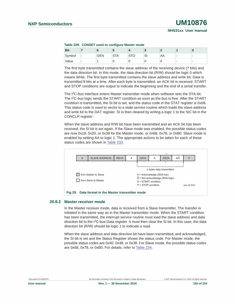
<Document ID>UM10876 All information provided in this document is subject to legal disclaimers. © NXP Semiconductors N.V. 2016. All rights reserved.
User manual Rev. 1 — 30 November 2016 150 of 234
NXP Semiconductors UM10876NHS31xx User manual
The first byte transmitted contains the slave address of the receiving device (7 bits) and the data direction bit. In this mode, the data direction bit (R/W) should be logic 0 which means Write. The first byte transmitted contains the slave address and write bit. Data is transmitted 8 bits at a time. After each byte is transmitted, an ACK bit is received. START and STOP conditions are output to indicate the beginning and the end of a serial transfer.
The I2C-bus interface enters Master transmitter mode when software sets the STA bit. The I2C-bus logic sends the START condition as soon as the bus is free. After the START condition is transmitted, the SI bit is set, and the status code in the STAT register is 0x08. This status code is used to vector to a state service routine which loads the slave address and write bit to the DAT register. SI is then cleared by writing a logic 1 to the SIC bit in the CONCLR register.
When the slave address and R/W bit have been transmitted and an ACK bit has been received, the SI bit is set again. If the Slave mode was enabled, the possible status codes are now 0x18, 0x20, or 0x38 for the Master mode, or 0x68, 0x78, or 0xB0. Slave mode is enabled by setting AA to logic 1. The appropriate actions to be taken for each of these status codes are shown in Table 233.
20.8.2 Master receiver modeIn the Master receiver mode, data is received from a Slave transmitter. The transfer is initiated in the same way as in the Master transmitter mode. When the START condition has been transmitted, the interrupt service routine must load the slave address and data direction bit to the I2C-bus Data register. It must then clear the SI bit. In this case, the data direction bit (R/W) should be logic 1 to indicate a read.
When the slave address and data direction bit have been transmitted, and acknowledged, the SI bit is set and the Status Register shows the status code. For Master mode, the possible status codes are 0x40, 0x48, or 0x38. For Slave mode, the possible status codes are 0x68, 0x78, or 0xB0. For details, refer to Table 234.
Table 229. CONSET used to configure Master modeBit 7 6 5 4 3 2 1 0Symbol - I2EN STA STO SI AA - -
Value - 1 0 0 0 0 - -
Fig 29. Data format in the Master transmitter mode
aaa-017870
SLAVE ADDRESS RW=0 A A
n bytes data transmitted
A = Acknowledge (SDA low)A = Not acknowledge (SDA high)
from Master to Slave
from Slave to Master S = START conditionP = STOP condition
A/A PS DATA DATA

<Document ID>UM10876 All information provided in this document is subject to legal disclaimers. © NXP Semiconductors N.V. 2016. All rights reserved.
User manual Rev. 1 — 30 November 2016 151 of 234
NXP Semiconductors UM10876NHS31xx User manual
After a Repeated-START condition, I2C-bus may switch to the Master transmitter mode:
20.8.3 Slave receiver modeIn the Slave receiver mode, data bytes are received from a master transmitter. To initialize the Slave receiver mode, write any of the Slave Address Registers (ADR0-3) and write the I2C-bus Control Set register (CONSET) as shown in Table 230.
I2EN must be set to logic 1 to enable the I2C-bus function. AA bit must be set to logic 1 to acknowledge its own slave address or the General Call address. The STA, STO and SI bits are set to logic 1.
After ADR and CONSET are initialized, the I2C-bus interface waits until addressed by its own address or general address followed by the data direction bit. If the direction bit is logic 0 (Write), it enters Slave receiver mode. If the direction bit is logic 1 (Read), it enters Slave transmitter mode. After the address and direction bit have been received, the SI bit is set. A valid status code can now be read from the Status register (STAT). Refer to Table 237 for the status codes and actions.
Fig 30. Data format of Master receiver mode
Fig 31. Master receiver switches to master transmitter after sending Repeated-START
aaa-017878
SLAVE ADDRESS RW=1 A A
n bytes data received
A = Acknowledge (SDA low)A = Not acknowledge (SDA high)
from Master to Slave
from Slave to Master S = START conditionP = STOP condition
A PS DATA DATA
aaa-017871
n bytes data transmitted
A = Acknowledge (SDA low)A = Not acknowledge (SDA high)
from Master to Slave
from Slave to Master S = START conditionP = STOP conditionSLA = Slave AddressSr = Repeated START condition
S R A SrA W A AA PSLA SLADATA DATA DATA
Table 230. CONSET used to configure Slave modeBit 7 6 5 4 3 2 1 0Symbol - I2EN STA STO SI AA - -
Value - 1 0 0 0 1 - -

<Document ID>UM10876 All information provided in this document is subject to legal disclaimers. © NXP Semiconductors N.V. 2016. All rights reserved.
User manual Rev. 1 — 30 November 2016 152 of 234
NXP Semiconductors UM10876NHS31xx User manual
20.8.4 Slave transmitter modeThe first byte is received and handled as in the Slave receiver mode. However, in this mode, the direction bit is logic 1, indicating a read operation. Serial data is transmitted via SDA while the serial clock is input through SCL. START and STOP conditions are recognized as the beginning and end of a serial transfer. In a given application, I2C-busmay operate as a master and as a slave.
In the Slave mode, the I2C-bus hardware looks for its own slave address and the General Call address. If one of these addresses is detected, an interrupt is requested. When the microcontroller wishes to become the bus master, the hardware waits until the bus is free before the Master mode is entered. This wait state is to ensure that a possible slave action is not interrupted. If bus arbitration is lost in Master mode, the I2C-bus block immediately switches to Slave mode. It can then detect its own slave address in the same serial transfer.
Fig 32. Data format of Slave receiver mode
SLAVE ADDRESS RW=0 A A
n bytes data received
A = Acknowledge (SDA low)A = Not acknowledge (SDA high)
from Master to Slave
from Slave to Master S = START conditionP = STOP condition
aaa-017876Sr = Repeated START condition
A/A P/SrS DATA DATA
Fig 33. Data format of Slave mode
aaa-017880
SLAVE ADDRESS RW=1 A A
n bytes data transmitted
A = Acknowledge (SDA low)A = Not acknowledge (SDA high)
from Master to Slave
from Slave to Master S = START conditionP = STOP condition
A PS DATA DATA
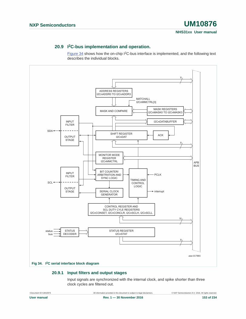
<Document ID>UM10876 All information provided in this document is subject to legal disclaimers. © NXP Semiconductors N.V. 2016. All rights reserved.
User manual Rev. 1 — 30 November 2016 153 of 234
NXP Semiconductors UM10876NHS31xx User manual
20.9 I2C-bus implementation and operation.Figure 34 shows how the on-chip I2C-bus interface is implemented, and the following text describes the individual blocks.
20.9.1 Input filters and output stagesInput signals are synchronized with the internal clock, and spike shorter than three clock cycles are filtered out.
Fig 34. I2C serial interface block diagram
aaa-017881
INPUTFILTER
OUTPUTSTAGE
MONITOR MODEREGISTER
I2CnMMCTRL
INPUTFILTER
OUTPUTSTAGE
STATUSDECODER
statusbus
SCL
SDA
BIT COUNTER/ARBITRATION AND
SYNC LOGICTIMING ANDCONTROL
LOGIC
PCLK
ACK
interruptSERIAL CLOCKGENERATOR
SHIFT REGISTERI2CnDAT
CONTROL REGISTER ANDSCL DUTY CYLE REGISTERS
I2CnCONSET, I2CnCONCLR, I2CnSCLH, I2CnSCLL
STATUS REGISTERI2CnSTAT
MASK AND COMPARE
ADDRESS REGISTERSI2CnADDR0 TO I2CnADDR3
MASK REGISTERSI2CnMASK0 TO I2CnMASK3
APBBUS
MATCHALLI2CnMMCTRL[3]
I2CnDATABUFFER
8
16
8
8

<Document ID>UM10876 All information provided in this document is subject to legal disclaimers. © NXP Semiconductors N.V. 2016. All rights reserved.
User manual Rev. 1 — 30 November 2016 154 of 234
NXP Semiconductors UM10876NHS31xx User manual
The output for I2C-bus is a special pad designed to conform to the I2C-bus specification.
20.9.2 Address Registers, ADDR0 to ADDR3These registers may be loaded with the 7-bit slave address (7 MSBs) to which the I2C-busblock responds when programmed as a slave transmitter or receiver. The LSB (GC) is used to enable General Call address (0x00) recognition. When multiple slave addresses are enabled, the actual address received may be read from the DAT register at the state where the own slave address has been received.
20.9.3 Address mask registers, MASK0 to MASK3The four mask registers each contain seven active bits (7:1). Any bit in these registers which is set to logic 1, causes an automatic compare. It compares the corresponding bit of the received address with the ADDRn register associated with that mask register. In other words, bits in an ADDRn register which are masked are not considered when determining an address match.
When an address-match interrupt occurs, the processor has to read the data register (DAT) to determine what the received address was that caused the match.
20.9.4 ComparatorThe comparator compares the received 7-bit slave address with its own slave address (7 most significant bits in ADR). It also compares the first received 8-bit byte with the General Call address (0x00). If an equality is found, the appropriate status bits are set and an interrupt is requested.
20.9.5 Shift register, DATThis 8-bit register contains a byte of serial data to be transmitted or a byte which has been received. Data in DAT is always shifted from right to left. The first bit transmitted is the MSB (bit 7). After a byte has been received, the first bit of received data is at the MSB of DAT. While data is being shifted out, data on the bus is simultaneously being shifted in; DAT always contains the last byte present on the bus. Thus, in the event of lost arbitration, the transition from master transmitter to slave receiver is made with the correct data in DAT.
20.9.6 Arbitration and synchronization logicIn the Master transmitter mode, the arbitration logic checks that every transmitted logic 1 actually appears as a logic 1 on the I2C-bus. If another device on the bus overrules a logic 1 and pulls the SDA line low, arbitration is lost. The I2C-bus block immediately changes from master transmitter to slave receiver. The I2C-bus block continues to output clock pulses (on SCL) until transmission of the current serial byte is complete.
Arbitration may also be lost in the Master receiver mode. Loss of arbitration in this mode can only occur while the I2C-bus block is returning a ’not acknowledge’ (logic 1) to the bus. Arbitration is lost when another device on the bus pulls this signal low. Since this case can occur only at the end of a serial byte, the I2C-bus block generates no further clock pulses. Figure 35 shows the arbitration procedure.
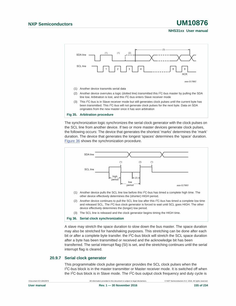
<Document ID>UM10876 All information provided in this document is subject to legal disclaimers. © NXP Semiconductors N.V. 2016. All rights reserved.
User manual Rev. 1 — 30 November 2016 155 of 234
NXP Semiconductors UM10876NHS31xx User manual
The synchronization logic synchronizes the serial clock generator with the clock pulses on the SCL line from another device. If two or more master devices generate clock pulses, the following occurs: The device that generates the shortest ’marks’ determines the ’mark’ duration. The device that generates the longest ’spaces’ determines the ’space’ duration. Figure 36 shows the synchronization procedure.
A slave may stretch the space duration to slow down the bus master. The space duration may also be stretched for handshaking purposes. This stretching can be done after each bit or after a complete byte transfer. the I2C-bus block will stretch the SCL space duration after a byte has been transmitted or received and the acknowledge bit has been transferred. The serial interrupt flag (SI) is set, and the stretching continues until the serial interrupt flag is cleared.
20.9.7 Serial clock generatorThis programmable clock pulse generator provides the SCL clock pulses when the I2C-bus block is in the master transmitter or Master receiver mode. It is switched off when the I2C-bus block is in Slave mode. The I2C-bus output clock frequency and duty cycle is
(1) Another device transmits serial data(2) Another device overrules a logic (dotted line) transmitted this I2C-bus master by pulling the SDA
line low. Arbitration is lost, and this I2C-bus enters Slave receiver mode(3) This I2C-bus is in Slave receiver mode but still generates clock pulses until the current byte has
been transmitted. This I2C-bus will not generate clock pulses for the next byte. Data on SDA originates from the new master once it has won arbitration
Fig 35. Arbitration procedure
(1) Another device pulls the SCL line low before this I2C-bus has timed a complete high time. The other device effectively determines the (shorter) HIGH period.
(2) Another device continues to pull the SCL line low after this I2C-bus has timed a complete low time and released SCL. The I2C-bus clock generator is forced to wait until SCL goes HIGH. The other device effectively determines the (longer) low period.
(3) The SCL line is released and the clock generator begins timing the HIGH time.
Fig 36. Serial clock synchronization
aaa-017882
84321 9
ACK
SCL line
SDA line(1) (1) (2)
(3)
aaa-017883
SDA line
SCL line
(1)
highperiod
lowperiod
(3)
(2)
(1)

<Document ID>UM10876 All information provided in this document is subject to legal disclaimers. © NXP Semiconductors N.V. 2016. All rights reserved.
User manual Rev. 1 — 30 November 2016 156 of 234
NXP Semiconductors UM10876NHS31xx User manual
programmable via the I2C-bus Clock Control Registers. See the description of the I2CSCLL and I2CSCLH registers for details. The output clock pulses have a duty cycle as programmed unless the bus is synchronizing with other SCL clock sources as described above.
20.9.8 Timing and controlThe timing and control logic generates the timing and control signals for serial byte handling. This logic block performs the following tasks:
• Provides the shift pulses for DAT• Enables the comparator• Generates and detects START and STOP conditions• Receives and transmits acknowledge bits• Controls the Master and Slave modes• Contains interrupt request logic• Monitors the I2C-bus status
20.9.9 Control register, CONSET and CONCLR
The I2C-bus control register contains bits used to control the following I2C block functions: start and restart of a serial transfer, termination of a serial transfer, bit rate, address recognition, and acknowledgment.
The contents of the I2C-bus control register may be read as CONSET. Writing to CONSET sets bits in the I2C-bus control register that correspond to ones in the value written. Conversely, writing to CONCLR clears bits in the I2C-bus control register that correspond to ones in the value written.
20.9.10 Status decoder and status registerThe status decoder takes all of the internal status bits and compresses them into a 5-bit code. This code is unique for each I2C-bus status. The 5-bit code may be used to generate vector addresses for fast processing of the various service routines. Each service routine processes a particular bus status. There are 26 possible bus states if all four modes of the I2C-bus block are used. The 5-bit status code is latched into the five most significant bits of the status register when the serial interrupt flag is set (by hardware). It remains stable until software clears the interrupt flag. The three least significant bits of the status register are always logic 0. If the status code is used as a vector to service routines, then eight address locations displace the routines. 8 bytes of code is sufficient for most of the service routines.
20.10 Details of I2C-bus operating modesAs mentioned above, there are four operating modes. These modes are:
• Master transmitter• Master receiver• Slave receiver• Slave transmitter

<Document ID>UM10876 All information provided in this document is subject to legal disclaimers. © NXP Semiconductors N.V. 2016. All rights reserved.
User manual Rev. 1 — 30 November 2016 157 of 234
NXP Semiconductors UM10876NHS31xx User manual
Data transfers in each mode of operation are shown in Figure 37, Figure 38, Figure 39,Figure 40 and Figure 41.
Table 231 lists abbreviations used in these figures when describing the I2C-bus operating modes.
In Figure 37 to Figure 41, circles are used to indicate when the serial interrupt flag is set. The numbers in the circles show the status code held in the STAT register. At these points, a service routine must be executed to continue or complete the serial transfer. These service routines are not critical since the serial transfer is suspended until software clears the serial interrupt flag.
When a serial interrupt routine is entered, the status code in STAT is used to branch to the appropriate service routine. For each status code, the required software action and details of the following serial transfer are given in tables from Table 233 to Table 239.
20.10.1 Master transmitter modeIn the Master transmitter mode, a number of data bytes are transmitted to a slave receiver (see Figure 37). Before the Master transmitter mode can be entered, The CONSET register must be initialized as follows:
Also, the I2C-bus rate must be configured in the SCLL and SCLH registers. I2EN must be set to logic 1 to enable the I2C-bus block. If the AA bit is reset, the I2C-bus block does not acknowledge its own slave address. In the event of another device becoming master of the bus, it does not acknowledge the General Call address. In other words, if AA is reset, the I2C-bus interface cannot enter Slave mode. STA, STO, and SI must be reset.
The Master transmitter mode may now be entered by setting the STA bit. The I2C logic now tests the I2C-bus and generate a START condition as soon as the bus becomes free. When a START condition is transmitted, the serial interrupt flag (SI) is set, and the status code in the status register (STAT) is 0x08. This status code is used by the interrupt service routine to enter the appropriate state service routine. This routine loads DAT with the slave address and the data direction bit (SLA+W). The SI bit in CON must then be reset before the serial transfer can continue.
Table 231. Abbreviations used to describe an I2C-bus operationAbbreviation ExplanationS START Condition
SLA 7-bit slave address
R read bit (HIGH level at SDA)
W write bit (low level at SDA)
A acknowledge bit (Low level at SDA)
A not acknowledge bit (HIGH level at SDA)
Data 8-bit data byte
P STOP condition
Table 232. CONSET used to initialize Master transmitter modeBIT 7 6 5 4 3 2 1 0Symbol - I2EN STA STO SI AA - -
Value - 1 0 0 0 X - -
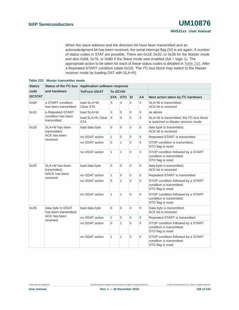
<Document ID>UM10876 All information provided in this document is subject to legal disclaimers. © NXP Semiconductors N.V. 2016. All rights reserved.
User manual Rev. 1 — 30 November 2016 158 of 234
NXP Semiconductors UM10876NHS31xx User manual
When the slave address and the direction bit have been transmitted and an acknowledgment bit has been received, the serial interrupt flag (SI) is set again. A number of status codes in STAT are possible. There are 0x18, 0x20, or 0x38 for the Master mode and also 0x68, 0x78, or 0xB0 if the Slave mode was enabled (AA = logic 1). The appropriate action to be taken for each of these status codes is detailed in Table 233. After a Repeated-START condition (state 0x10). The I2C-bus block may switch to the Master receiver mode by loading DAT with SLA+R).
Table 233. Master transmitter modeStatuscodeI2CSTAT
Status of the I2C-busand hardware
Application software responseTo/From I2DAT To I2CON
STA STO SI AA Next action taken by I2C hardware0x08 a START condition
has been transmittedload SLA+W;Clear STA
X 0 0 X SLA+W is transmitted; ACK bit is received
0x10 a Repeated-START condition has been transmitted
load SLA+W X 0 0 X as above
load SLA+R; Clear STA
X 0 0 X SLA+W is transmitted; the I2C-bus block is switched to Master receiver mode
0x18 SLA+W has been transmitted; ACK has been received
load data byte 0 0 0 X data byte is transmitted;ACK bit is received
no I2DAT action 1 0 0 X Repeated-START is transmitted
no I2DAT action 0 1 0 X STOP condition is transmitted;STO flag is reset
no I2DAT action 1 1 0 X STOP condition followed by a START condition is transmitted; STO flag is reset
0x20 SLA+W has been transmitted; NACK has been received
load data byte 0 0 0 X data byte is transmitted; ACK bit is received
no I2DAT action 1 0 0 X Repeated-START is transmitted
no I2DAT action 0 1 0 X STOP condition followed by a START condition is transmitted; STO flag is reset
no I2DAT action 1 1 0 X STOP condition followed by a START condition is transmitted; STO flag is reset
0x28 data byte in I2DAT has been transmitted; ACK has been received.
load data byte 0 0 0 X Data byte is transmitted; ACK bit is received
no I2DAT action 1 0 0 X Repeated-START is transmitted
no I2DAT action 0 1 0 X STOP condition followed by a START condition is transmitted; STO flag is reset
no I2DAT action 1 1 0 X STOP condition followed by a START condition is transmitted; STO flag is reset

<Document ID>UM10876 All information provided in this document is subject to legal disclaimers. © NXP Semiconductors N.V. 2016. All rights reserved.
User manual Rev. 1 — 30 November 2016 159 of 234
NXP Semiconductors UM10876NHS31xx User manual
0x30 data byte in I2DAT has been transmitted; NOT ACK has been received.
load data byte 0 0 0 X data byte is transmitted; ACK bit is received
no I2DAT action 1 0 0 X repeated START is transmitted
no I2DAT action 0 1 0 X STOP condition followed by a START condition is transmitted; STO flag is reset
no I2DAT action 1 1 0 X STOP condition followed by a START condition is transmitted; STO flag is reset
0x38 arbitration lost in SLA+R/W or Data bytes
no I2DAT action 0 0 0 X I2C-bus is released; not addressed Slave mode is entered
no I2DAT action 1 0 0 X a START condition is transmitted when the bus becomes free
Table 233. Master transmitter mode _continued
StatuscodeI2CSTAT
Status of the I2C-busand hardware
Application software responseTo/From I2DAT To I2CON
STA STO SI AA Next action taken by I2C hardware

<Document ID>UM10876 All information provided in this document is subject to legal disclaimers. © NXP Semiconductors N.V. 2016. All rights reserved.
User manual Rev. 1 — 30 November 2016 160 of 234
NXP Semiconductors UM10876NHS31xx User manual
20.10.2 Master receiver modeIn the Master receiver mode, a number of data bytes are received from a slave transmitter (see Figure 38). The transfer is initialized as in the Master transmitter mode. When the START condition has been transmitted, the interrupt service routine must load DAT with the 7-bit slave address and the data direction bit (SLA+R). The SI bit in CON must then be cleared before the serial transfer can continue.
Fig 37. Format and states in the Master transmitter mode
aaa-017897
DATASLAS
successfultransmission
to a SlaveReceiver
next transferstarted with a
Repeated Startcondition
NotAcknowledgereceived after
the Slave address
NotAcknowledgereceived after
a Data byte
arbitration lostin Slave address or
Data byte
arbitration lostand addressed
as Slave
08H 18H
W
MT
A A P
28H
SLAS W
R
A P
30H
10H
A P
20H
A
68H 78H 80H
A OR A
from Master to Slave
from Slave to Master
any number of data bytes and their associated Acknowledge bits
this number (contained in l2STA) corresponds to a defined state of the I2C bus
38H
A OR Aother Mastercontinues
other Mastercontinues
other Mastercontinues
to correspondingstates in Slave mode
to Masterreceive mode,
entry = MR
38H
DATA
n

<Document ID>UM10876 All information provided in this document is subject to legal disclaimers. © NXP Semiconductors N.V. 2016. All rights reserved.
User manual Rev. 1 — 30 November 2016 161 of 234
NXP Semiconductors UM10876NHS31xx User manual
When the slave address and data direction bit have been transmitted, and an acknowledgment bit has been received, the serial interrupt flag (SI) is set again. A number of status codes in STAT are then possible. If the Slave mode was enabled (AA = 1), then these codes are 0x40, 0x48, or 0x38 for the Master mode and also 0x68, 0x78, or 0xB0. The appropriate action to be taken for each of these status codes is detailed in Table 234.After a Repeated-START condition (state 0x10), the I2C-bus block may switch to the Master transmitter mode by loading DAT with SLA+W.
Table 234. Master receive modeStatuscodeI2CSTAT
Status of the I2C-busand hardware
Application software responseTo/From I2DAT To I2CON
STA STO SI AA Next action taken by I2C hardware0x08 A START condition
has been transmittedload SLA+W X 0 0 X SLA+R is transmitted;
ACK bit is received
0x10 A Repeated-START condition has been transmitted
load SLA+R X 0 0 X as above
load SLA+W X 0 0 X SLA+W is transmitted; the I2C block is switched to Master receiver mode
0x38 Arbitration lost in NACK bit
no I2DAT action 0 0 0 X I2C-bus is released; not addressed Slave mode is entered
no I2DAT action 1 0 0 X a START condition is transmitted when the bus becomes free
0x40 SLA+R has been transmitted;ACK has been received
load data byte 0 0 0 0 data byte is received;NACK bit is returned
no I2DAT action 0 0 0 1 data byte is received;ACK bit is returned
0x48 SLA+R has been transmitted;NACK has been received
no I2DAT action 1 0 0 X repeated START is transmitted
no I2DAT action 0 1 0 X STOP condition is transmitted;STO flag is reset
no I2DAT action 1 1 0 X STOP condition followed by a START condition is transmitted;STO flag is reset
0x50 Data byte has been received; ACK has been returned.
read data byte 0 0 0 0 data byte is received;NACK bit is returned
read data byte 0 0 0 1 data byte is received;ACK bit is returned
0x58 Data byte has been received;NACK has been returned.
read data byte 1 0 0 X repeated START condition is transmitted
read data byte 0 1 0 X a STOP condition is transmitted;STO flag is reset
read data byte 1 1 0 X STOP condition followed by a START condition is transmitted;STO flag is reset

<Document ID>UM10876 All information provided in this document is subject to legal disclaimers. © NXP Semiconductors N.V. 2016. All rights reserved.
User manual Rev. 1 — 30 November 2016 162 of 234
NXP Semiconductors UM10876NHS31xx User manual
20.10.3 Slave receiver modeIn the Slave receiver mode, a number of data bytes are received from a master transmitter (see Figure 39). To initiate the Slave receiver mode, ADR and CON must be loaded as follows:
Fig 38. Format and states in Master receiver mode
aaa-017898
DATASLAS
successfultransmission
to a Slavetransmitter
next transferstarted with a
Repeated Startcondition
NotAcknowledgereceived after
the Slave address
arbitration lostin Slave address or
Acknowledge bit
arbitration lostand addressed
as Slave
08H 40H
R
MR
A AA P
58H
SLAS R
W
50H
A
38H
10H
A P
48H
A
68H 78H 80H
A OR A
from Master to Slave
from Slave to Master
any number of data bytes and their associated Acknowledge bits
this number (contained in l2STA) corresponds to a defined state of the I2C bus
38H
other Mastercontinues
other Mastercontinues
to correspondingstates in Slave mode
to Mastertransmit mode,
entry = MT
DATA
DATA A
n
other Mastercontinues
Table 235. ADR usage in Slave receiver modeBIT 7 6 5 4 3 2 1 0Symbol own slave 7-bit address GC
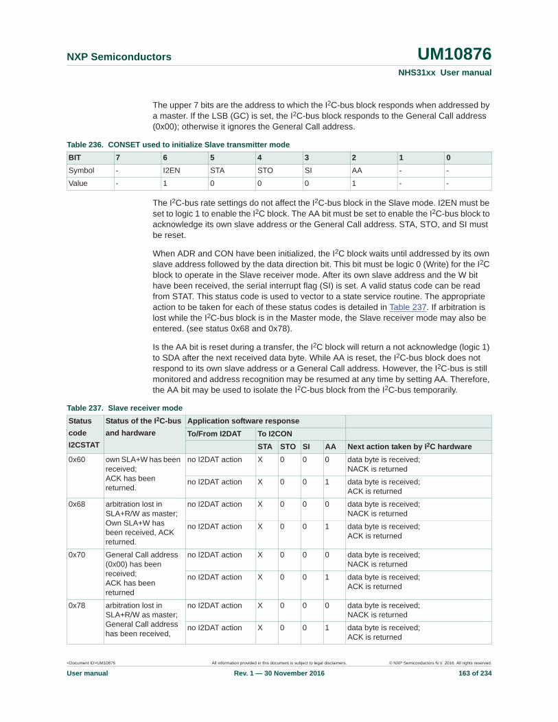
<Document ID>UM10876 All information provided in this document is subject to legal disclaimers. © NXP Semiconductors N.V. 2016. All rights reserved.
User manual Rev. 1 — 30 November 2016 163 of 234
NXP Semiconductors UM10876NHS31xx User manual
The upper 7 bits are the address to which the I2C-bus block responds when addressed by a master. If the LSB (GC) is set, the I2C-bus block responds to the General Call address (0x00); otherwise it ignores the General Call address.
The I2C-bus rate settings do not affect the I2C-bus block in the Slave mode. I2EN must be set to logic 1 to enable the I2C block. The AA bit must be set to enable the I2C-bus block to acknowledge its own slave address or the General Call address. STA, STO, and SI must be reset.
When ADR and CON have been initialized, the I2C block waits until addressed by its own slave address followed by the data direction bit. This bit must be logic 0 (Write) for the I2Cblock to operate in the Slave receiver mode. After its own slave address and the W bit have been received, the serial interrupt flag (SI) is set. A valid status code can be read from STAT. This status code is used to vector to a state service routine. The appropriate action to be taken for each of these status codes is detailed in Table 237. If arbitration is lost while the I2C-bus block is in the Master mode, the Slave receiver mode may also be entered. (see status 0x68 and 0x78).
Is the AA bit is reset during a transfer, the I2C block will return a not acknowledge (logic 1) to SDA after the next received data byte. While AA is reset, the I2C-bus block does not respond to its own slave address or a General Call address. However, the I2C-bus is still monitored and address recognition may be resumed at any time by setting AA. Therefore, the AA bit may be used to isolate the I2C-bus block from the I2C-bus temporarily.
Table 236. CONSET used to initialize Slave transmitter modeBIT 7 6 5 4 3 2 1 0Symbol - I2EN STA STO SI AA - -
Value - 1 0 0 0 1 - -
Table 237. Slave receiver modeStatuscodeI2CSTAT
Status of the I2C-busand hardware
Application software responseTo/From I2DAT To I2CON
STA STO SI AA Next action taken by I2C hardware0x60 own SLA+W has been
received;ACK has been returned.
no I2DAT action X 0 0 0 data byte is received;NACK is returned
no I2DAT action X 0 0 1 data byte is received;ACK is returned
0x68 arbitration lost in SLA+R/W as master; Own SLA+W has been received, ACK returned.
no I2DAT action X 0 0 0 data byte is received;NACK is returned
no I2DAT action X 0 0 1 data byte is received;ACK is returned
0x70 General Call address (0x00) has been received;ACK has been returned
no I2DAT action X 0 0 0 data byte is received;NACK is returned
no I2DAT action X 0 0 1 data byte is received;ACK is returned
0x78 arbitration lost in SLA+R/W as master; General Call address has been received,
no I2DAT action X 0 0 0 data byte is received;NACK is returned
no I2DAT action X 0 0 1 data byte is received;ACK is returned

<Document ID>UM10876 All information provided in this document is subject to legal disclaimers. © NXP Semiconductors N.V. 2016. All rights reserved.
User manual Rev. 1 — 30 November 2016 164 of 234
NXP Semiconductors UM10876NHS31xx User manual
0x80 previously addressed with own Slave address; DATA has been received; ACK has been returned.
read data byte X 0 0 0 data byte is received;NACK is returned
read data byte X 0 0 1 data byte is received;ACK is returned
0x88 previously addressed with own SLA; DATA byte has been received; NACK has been returned.
read data byte 0 0 0 0 switched to not addressed Slave mode; no recognition of own SLA or General Call address
read data byte 0 0 0 1 switched to not addressed Slave mode; Own SLA is recognized; If I2ADR[0] = logic 1, General Call address is recognized
read data byte 1 0 0 0 switched to not addressed Slave mode;No recognition of own SLA or General Call address. A START condition is transmitted when the bus becomes free
read data byte 1 0 0 1 switched to not addressed Slave mode; Own SLA is recognized; If I2ADR[0] = logic 1, general call address is recognized
0x90 previously addressed with General Call; DATA byte has been received;ACK has been returned.
read data byte X 0 0 0 data byte is received;NACK is returned
read data byte X 0 0 1 data byte is received;ACK is returned
0x98 previously addressed with General Call; DATA byte has been received;NACK has been returned.
read data byte 0 0 0 0 switched to not addressed Slave mode; no recognition of own SLA or General Call address
read data byte 0 0 0 1 switched to not addressed Slave mode; Own SLA is recognized; If I2ADR[0] = logic 1, General Call address is recognized
read data byte 1 0 0 0 switched to not addressed Slave mode; no recognition of own SLA or General Call address. A START condition is transmitted when the bus becomes free
read data byte 1 0 0 1 switched to not addressed Slave mode; Own SLA is recognized; If I2ADR[0] = logic 1, General Call address is recognized. A START condition is transmitted when the bus becomes free
Table 237. Slave receiver mode _continued
StatuscodeI2CSTAT
Status of the I2C-busand hardware
Application software responseTo/From I2DAT To I2CON
STA STO SI AA Next action taken by I2C hardware

<Document ID>UM10876 All information provided in this document is subject to legal disclaimers. © NXP Semiconductors N.V. 2016. All rights reserved.
User manual Rev. 1 — 30 November 2016 165 of 234
NXP Semiconductors UM10876NHS31xx User manual
0xA0 a STOP condition or Repeated-START condition has been received while still addressed as slave receiver or slave transmitter.
no STDAT action 0 0 0 0 switched to not addressed Slave mode; no recognition of own SLA or General Call address
no STDAT action 0 0 0 1 switched to not addressed Slave mode; Own SLA is recognized; If I2ADR[0] = logic 1, General Call address is recognized
no STDAT action 1 0 0 0 switched to not addressed Slave mode; no recognition of own SLA or General Call address. A START condition is transmitted when the bus becomes free
no STDAT action 1 0 0 1 switched to not addressed Slave mode;Own SLA is recognized; If I2ADR[0] = logic 1, General Call address is recognized. A START condition is transmitted when the bus becomes free
Table 237. Slave receiver mode _continued
StatuscodeI2CSTAT
Status of the I2C-busand hardware
Application software responseTo/From I2DAT To I2CON
STA STO SI AA Next action taken by I2C hardware

<Document ID>UM10876 All information provided in this document is subject to legal disclaimers. © NXP Semiconductors N.V. 2016. All rights reserved.
User manual Rev. 1 — 30 November 2016 166 of 234
NXP Semiconductors UM10876NHS31xx User manual
20.10.4 Slave transmitter modeIn the Slave transmitter mode, a number of data bytes are transmitted to a master receiver (see Figure 40). Data transfer is initialized as in the Slave receiver mode. When ADR and CON have been initialized, the I2C-bus block waits until it is addressed by its own slave address followed by the data direction bit. The data direction bit must be logic 1 (Read) for the I2C-bus block to operate in the Slave transmitter mode. After its own slave address and the R bit have been received, the serial interrupt flag (SI) is set and a valid status code can be read from STAT. This status code is used to vector to a state service routine,
Fig 39. Format and states in Slave receiver mode
aaa-017900
DATASLAS
reception of the ownSlave address and oneor more Data bytes all
are acknowledged
last data bytereceived is Notacknowledged
arbitration lost asMaster and addressed
as Slave
last data byte is Notacknowledged
arbitration lostas Master and addressedas Slave by General Call
60H
W A AA P OR S
80H
P OR S
80H A0H
88H
A
68H
from Master to Slave
from Slave to Master
any number of data bytes and their associated Acknowledge bits
this number (contained in l2STA) corresponds to a defined state of the I2C bus
reception of theGeneral Call address
and one or moreData bytes
DATA
DATA A
n
A
DATAGENERAL CALL
70H
A AA P OR S
90H90H A0H
98H
A
78H
DATA
A P OR S

<Document ID>UM10876 All information provided in this document is subject to legal disclaimers. © NXP Semiconductors N.V. 2016. All rights reserved.
User manual Rev. 1 — 30 November 2016 167 of 234
NXP Semiconductors UM10876NHS31xx User manual
and the appropriate action to be taken for each of these status codes is detailed in Table 238. If arbitration is lost while the I2C-bus block is in the Master mode (see state 0xB0), the Slave transmitter mode may also be entered.
If the AA bit is reset during a transfer, the I2C-bus block transmits the last byte of the transfer and enters state 0xC0 or 0xC8. If the master receiver continues the transfer, the I2C block is switched to the not-addressed Slave mode and ignores the master receiver.
Thus the master receiver receives all logic 1s as serial data. While AA is reset, the I2C-bus block does not respond to its own slave address or a General Call address. However, the I2C-bus is still monitored, and address recognition may be resumed at any time by setting AA. This action means that the AA bit may be used to isolate the I2C-bus block from the I2C-bus temporarily.
Table 238. Slave transmitter modeStatus code I2CSTAT
Status of the I2C-busand hardware
Application software responseTo/From I2DAT To I2CON
STA STO SI AA Next action taken by I2C-bus hardware0xA8 own SLA+R has been
received;ACK has been returned.
load data byte X 0 0 0 data byte is transmitted;NACK is received
load data byte X 0 0 1 data byte is transmitted;ACK is received
0xB0 arbitration lost in SLA+R/W as master; Own SLA+W has been received, ACK returned.
load data byte X 0 0 0 data byte is transmitted;NACK is received
load data byte X 0 0 1 data byte is transmitted;ACK is received
0xB8 data byte in I2DAT has been transmitted; ACK has been received.
load data byte X 0 0 0 data byte is transmitted;NACK is received
load data byte X 0 0 1 data byte is transmitted;ACK is received
0xC0 data byte in I2DAT has been transmitted; NACK has been received.
no I2DAT action 0 0 0 0 switched to not addressed Slave mode; no recognition of own SLA or General Call address
no I2DAT action 0 0 0 1 switched to not addressed Slave mode; Own SLA is recognized; If I2ADR[0] = logic 1, General Call address is recognized
no I2DAT action 1 0 0 0 switched to not addressed Slave mode; no recognition of own SLA or General Call address. A START condition is transmitted when the bus becomes free
no I2DAT action 1 0 0 1 switched to not addressed Slave mode; Own SLA is recognized; If I2ADR[0] = logic 1, General Call address is recognized. A START condition is transmitted when the bus becomes free

<Document ID>UM10876 All information provided in this document is subject to legal disclaimers. © NXP Semiconductors N.V. 2016. All rights reserved.
User manual Rev. 1 — 30 November 2016 168 of 234
NXP Semiconductors UM10876NHS31xx User manual
0xC8 last data byte in I2DAT has been transmitted (AA = 0); ACK has been received.
no I2DAT action 0 0 0 0 switched to not addressed Slave mode; no recognition of own SLA or General Call address
no I2DAT action 0 0 0 1 switched to not addressed Slave mode; Own SLA is recognized; If I2ADR[0] = logic 1, General Call address is recognized
no I2DAT action 1 0 0 0 switched to not addressed Slave mode; no recognition of own SLA or General Call address. A START condition is transmitted when the bus becomes free
no I2DAT action 1 0 0 1 switched to not addressed Slave mode; Own SLA is recognized; If I2ADR[0] = logic 1, General Call address is recognized. A START condition is transmitted when the bus becomes free
Table 238. Slave transmitter mode _continued
Status code I2CSTAT
Status of the I2C-busand hardware
Application software responseTo/From I2DAT To I2CON
STA STO SI AA Next action taken by I2C-bus hardware
Fig 40. Format and states in Slave transmitter mode
aaa-017907
arbitration lost asMaster and
addressed as Slave
last data bytetransmitted. Switched
to Not AddressedSlave (AA bit in
l2CON = “0”)
from Master to Slave
from Slave to Master
any number of data bytes and their associated Acknowledge bits
this number (contained in l2STA) corresponds to a defined state of the I2C bus
reception of the ownSlave address andone or more Data
bytes all areacknowledged
DATA A
n
DATASLA
A8H
AS R A P OR S
C0HB8H
C8H
80H
DATA
A P OR SALL ONES
A
A
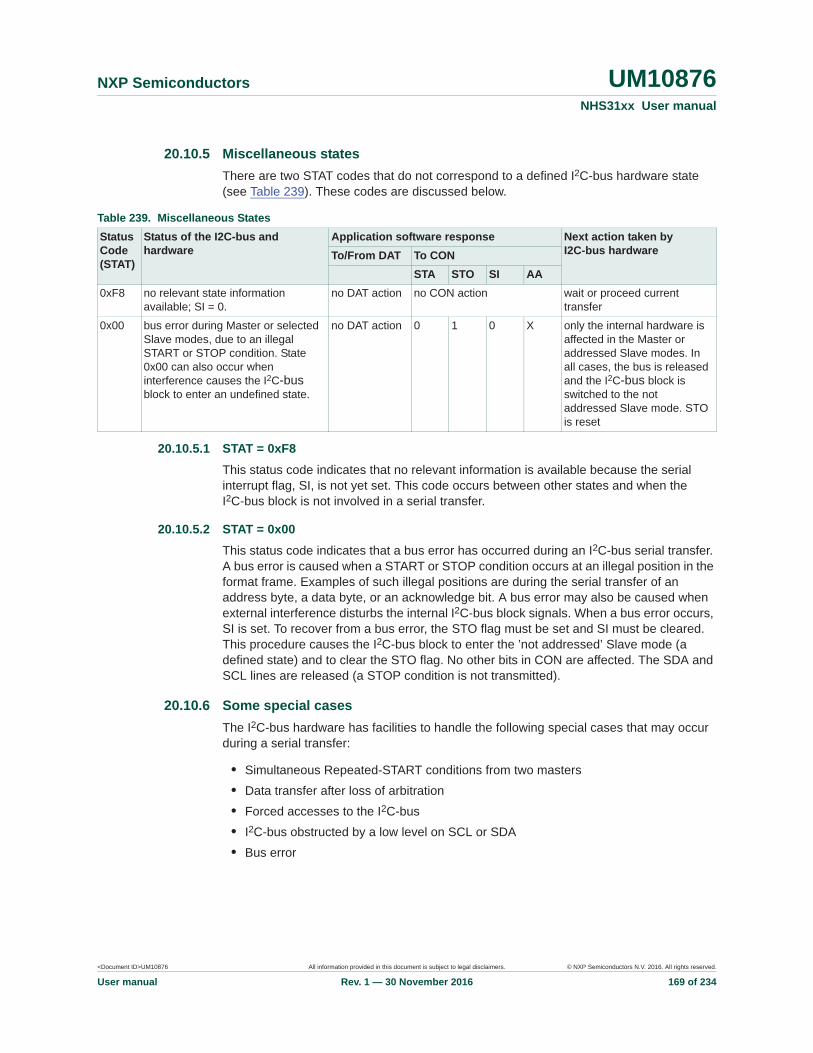
<Document ID>UM10876 All information provided in this document is subject to legal disclaimers. © NXP Semiconductors N.V. 2016. All rights reserved.
User manual Rev. 1 — 30 November 2016 169 of 234
NXP Semiconductors UM10876NHS31xx User manual
20.10.5 Miscellaneous statesThere are two STAT codes that do not correspond to a defined I2C-bus hardware state (see Table 239). These codes are discussed below.
20.10.5.1 STAT = 0xF8This status code indicates that no relevant information is available because the serial interrupt flag, SI, is not yet set. This code occurs between other states and when the I2C-bus block is not involved in a serial transfer.
20.10.5.2 STAT = 0x00This status code indicates that a bus error has occurred during an I2C-bus serial transfer. A bus error is caused when a START or STOP condition occurs at an illegal position in the format frame. Examples of such illegal positions are during the serial transfer of an address byte, a data byte, or an acknowledge bit. A bus error may also be caused when external interference disturbs the internal I2C-bus block signals. When a bus error occurs, SI is set. To recover from a bus error, the STO flag must be set and SI must be cleared. This procedure causes the I2C-bus block to enter the ’not addressed’ Slave mode (a defined state) and to clear the STO flag. No other bits in CON are affected. The SDA and SCL lines are released (a STOP condition is not transmitted).
20.10.6 Some special casesThe I2C-bus hardware has facilities to handle the following special cases that may occur during a serial transfer:
• Simultaneous Repeated-START conditions from two masters• Data transfer after loss of arbitration• Forced accesses to the I2C-bus• I2C-bus obstructed by a low level on SCL or SDA• Bus error
Table 239. Miscellaneous StatesStatus Code (STAT)
Status of the I2C-bus and hardware
Application software response Next action taken by I2C-bus hardwareTo/From DAT To CON
STA STO SI AA0xF8 no relevant state information
available; SI = 0.no DAT action no CON action wait or proceed current
transfer
0x00 bus error during Master or selected Slave modes, due to an illegal START or STOP condition. State 0x00 can also occur when interference causes the I2C-busblock to enter an undefined state.
no DAT action 0 1 0 X only the internal hardware is affected in the Master or addressed Slave modes. In all cases, the bus is released and the I2C-bus block is switched to the not addressed Slave mode. STO is reset
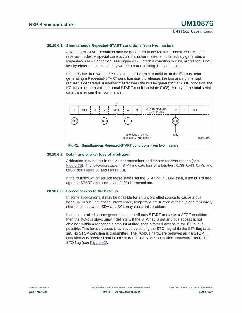
<Document ID>UM10876 All information provided in this document is subject to legal disclaimers. © NXP Semiconductors N.V. 2016. All rights reserved.
User manual Rev. 1 — 30 November 2016 170 of 234
NXP Semiconductors UM10876NHS31xx User manual
20.10.6.1 Simultaneous Repeated-START conditions from two mastersA Repeated-START condition may be generated in the Master transmitter or Master receiver modes. A special case occurs if another master simultaneously generates a Repeated-START condition (see Figure 41). Until this condition occurs, arbitration is not lost by either master since they were both transmitting the same data.
If the I2C-bus hardware detects a Repeated-START condition on the I2C-bus before generating a Repeated-START condition itself, it releases the bus and no interrupt request is generated. If another master frees the bus by generating a STOP condition, the I2C-bus block transmits a normal START condition (state 0x08). A retry of the total serial data transfer can then commence.
20.10.6.2 Data transfer after loss of arbitrationArbitration may be lost in the Master transmitter and Master receiver modes (see Figure 35). The following states in STAT indicate loss of arbitration: 0x38, 0x68, 0x78, and 0xB0 (see Figure 37 and Figure 38).
If the routines which service these states set the STA flag in CON, then, if the bus is free again, a START condition (state 0x08) is transmitted.
20.10.6.3 Forced access to the I2C-busIn some applications, it may be possible for an uncontrolled source to cause a bus hang-up. In such situations, interference, temporary interruption of the bus or a temporary short-circuit between SDA and SCL may cause this problem.
If an uncontrolled source generates a superfluous START or masks a STOP condition, then the I2C-bus stays busy indefinitely. If the STA flag is set and bus access is not obtained within a reasonable amount of time, then a forced access to the I2C-bus is possible. This forced access is achieved by setting the STO flag while the STA flag is still set. No STOP condition is transmitted. The I2C-bus hardware behaves as if a STOP condition was received and is able to transmit a START condition. Hardware clears the STO flag (see Figure 42).
Fig 41. Simultaneous Repeated-START conditions from two masters
aaa-017909
SLA S OTHER MASTERCONTINUES P S SLA
other Master sendsrepeated START earlier
retry
S W A ADATA
08H 18H 28H 08H
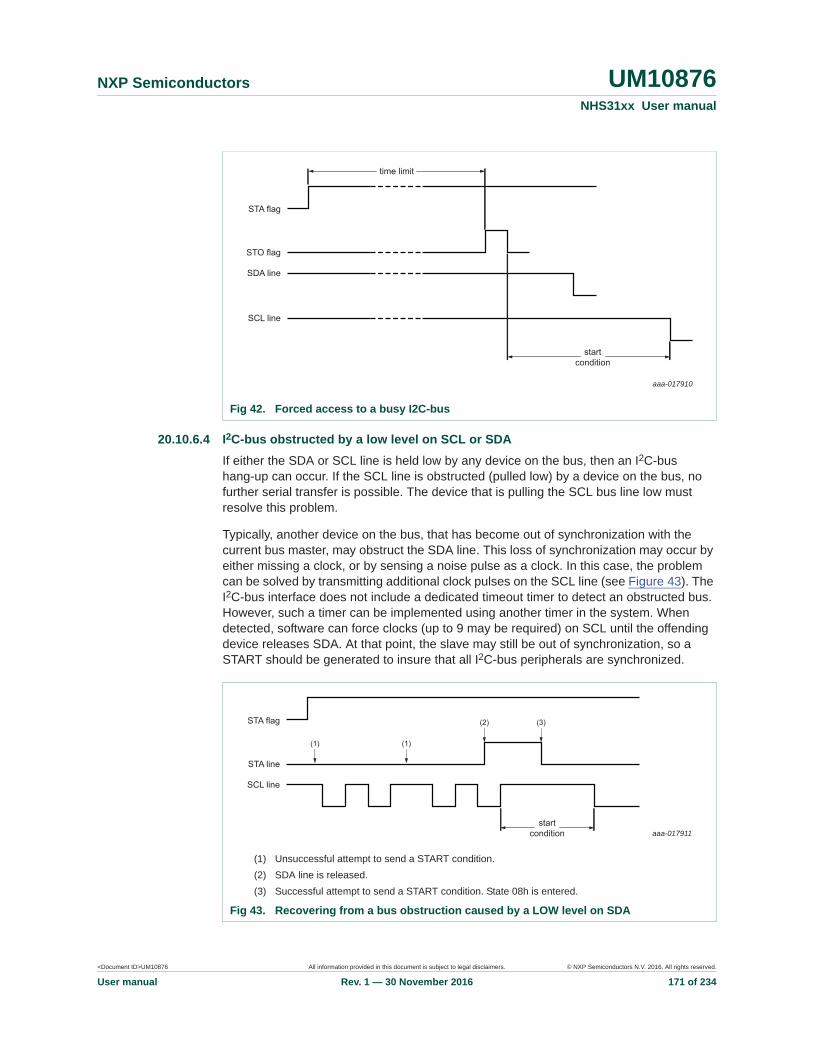
<Document ID>UM10876 All information provided in this document is subject to legal disclaimers. © NXP Semiconductors N.V. 2016. All rights reserved.
User manual Rev. 1 — 30 November 2016 171 of 234
NXP Semiconductors UM10876NHS31xx User manual
20.10.6.4 I2C-bus obstructed by a low level on SCL or SDAIf either the SDA or SCL line is held low by any device on the bus, then an I2C-bus hang-up can occur. If the SCL line is obstructed (pulled low) by a device on the bus, no further serial transfer is possible. The device that is pulling the SCL bus line low must resolve this problem.
Typically, another device on the bus, that has become out of synchronization with the current bus master, may obstruct the SDA line. This loss of synchronization may occur by either missing a clock, or by sensing a noise pulse as a clock. In this case, the problem can be solved by transmitting additional clock pulses on the SCL line (see Figure 43). The I2C-bus interface does not include a dedicated timeout timer to detect an obstructed bus. However, such a timer can be implemented using another timer in the system. When detected, software can force clocks (up to 9 may be required) on SCL until the offending device releases SDA. At that point, the slave may still be out of synchronization, so a START should be generated to insure that all I2C-bus peripherals are synchronized.
Fig 42. Forced access to a busy I2C-bus
aaa-017910
STA flag
STO flag
SDA line
SCL line
time limit
startcondition
(1) Unsuccessful attempt to send a START condition.(2) SDA line is released.(3) Successful attempt to send a START condition. State 08h is entered.
Fig 43. Recovering from a bus obstruction caused by a LOW level on SDA
aaa-017911
STA flag
STA line
SCL line
startcondition
(1) (1)
(2) (3)

<Document ID>UM10876 All information provided in this document is subject to legal disclaimers. © NXP Semiconductors N.V. 2016. All rights reserved.
User manual Rev. 1 — 30 November 2016 172 of 234
NXP Semiconductors UM10876NHS31xx User manual
20.10.6.5 Bus error
A bus error occurs when a START or STOP condition is detected at an illegal position in the format frame. Examples of illegal positions are during the serial transfer of an address byte, a data bit, or an acknowledge bit.
The I2C-bus hardware only reacts to a bus error when it is involved in a serial transfer either as a master or an addressed slave. When a bus error is detected, the I2C-bus block immediately switches to the not addressed Slave mode. It then releases the SDA and SCL lines, sets the interrupt flag, and loads the status register with 0x00. This status code may be used to vector to a state service routine which either attempts the aborted serial transfer again or simply recovers from the error condition as shown in Table 239.
20.10.7 I2C-bus state service routinesThis section provides examples of operations that the various I2C-bus state service routines must. These operations include:
• Initialization of the I2C-bus block after a reset• I2C-bus Interrupt Service• The 26 state service routines support all four I2C-bus operating modes
20.10.8 InitializationIn the initialization example, the I2C-bus block is enabled for both Master and Slave modes. For each mode, a buffer is used for transmission and reception. The initialization routine performs the following functions:
• The slave address of the part, and the General Call bit (GC), are loaded into ADR• The I2C-bus interrupt enable and interrupt priority bits are set• Simultaneously setting the I2EN and AA bits in CON enables the Slave mode. • Loading the SCLH and SCLL registers defines the serial clock frequency (for Master
modes). The master routines must be started in the main program
The I2C-bus hardware now begins checking the I2C-bus for its own slave address and General Call. If the General Call or the own slave address is detected, an interrupt is requested and STAT is loaded with the appropriate state information.
20.10.9 I2C-bus interrupt serviceWhen the I2C-bus interrupt is entered, STAT contains a status code which identifies one of the 26 state services to be executed.
20.10.10 The state service routinesEach state routine is part of the I2C-bus interrupt routine and handles one of the 26 states.
20.10.11 Adapting state services to an applicationThe state service examples show the typical actions that must be performed in response to the 26 I2C-bus state codes. If one or more of the four I2C-bus operating modes are not used, the associated state services can be omitted, as long as care is taken that those states can never occur.

<Document ID>UM10876 All information provided in this document is subject to legal disclaimers. © NXP Semiconductors N.V. 2016. All rights reserved.
User manual Rev. 1 — 30 November 2016 173 of 234
NXP Semiconductors UM10876NHS31xx User manual
In an application, it may be desirable to implement a timeout during I2C-bus operations to trap an inoperative bus or a lost service routine.

<Document ID>UM10876 All information provided in this document is subject to legal disclaimers. © NXP Semiconductors N.V. 2016. All rights reserved.
User manual Rev. 1 — 30 November 2016 174 of 234
NXP Semiconductors UM10876NHS31xx User manual
21. Serial Wire Debug
21.1 About this chapterThis chapter describes the features of the implemented Serial Wire Debug (SWD).
21.2 IntroductionSWD provides a clock (SWCLK) plus single bidirectional data (SWDIO) connection. This data connection provides all the normal JTAG debug and test functionality. It also provides real-time access to system memory, without halting the processor or requiring any target resident code. SWD uses an ARM standard bidirectional wire protocol to pass data between the debugger and the target system in a highly efficient and standard way. This protocol is defined in ARM Debug Interface v5.
21.3 FeaturesThe ARM Cortex-M0+ is configured to support up to four breakpoints and two watchpoints.
• Supports ARM SWD mode• Direct debug access to all memories, registers, and peripherals• No target resources are required for the debugging session• Four breakpoints. Four instruction breakpoints that can also be used to remap
instruction addresses for code patches. Two data comparators that can be used to remap addresses for patches to literal values
• Two data watchpoints that can also be used as triggers
Resetting the chip does not reset the Debug Access Point.
Remark: If a debug session is in progress, do not reset the chip.

<Document ID>UM10876 All information provided in this document is subject to legal disclaimers. © NXP Semiconductors N.V. 2016. All rights reserved.
User manual Rev. 1 — 30 November 2016 175 of 234
NXP Semiconductors UM10876NHS31xx User manual
22. Serial Peripheral Interface
22.1 About this chapterThis chapter describes the Serial Peripheral Interface (SPI). (APB 0x4004 0000).
22.2 Features
• compatible with Motorola SPI, 4-wire TI SSI, and National Semiconductor Microwire buses
• Synchronous Serial Communication• Supports master or slave operation• Eight-frame FIFOs for both transmit and receive• 4-bit to 16-bit frame
22.3 General descriptionThe SPI/SSP is a Synchronous Serial Port (SSP) controller capable of operation on an SPI, 4-wire SSI, or Microwire bus. It can interact with multiple masters and slaves on the bus. Only a single master and a single slave can communicate on the bus during a given data transfer. Data transfers are in principle full duplex, with frames of 4 bits to 16 bits of bidirectional data flowing between master and slave. In practice, often only one of these two data flows carries meaningful data.
22.4 ConfigurationThe Serial Peripheral Interface is configured using the following registers:
• Pins: The SPI pins must be configured in the IOCON register bock. In addition, use the IOCON_LOC register to select a Location for the SCLK function
• Power: In the SYSAHBCLKCTRL register, set bit 7 and bit 18• Peripheral clock: Enable the SPI peripheral clock by writing to the SSPCLKDIV
registers• Reset: Before accessing the SPI blocks, ensure that the SSP_RST_N bits (bit 0 and
bit 2) in the PRESETCTRL register (Table 8) is set to 1. This procedure de-asserts the reset signal to the SPI blocks
22.5 Pin description
Table 240. SPI pin descriptionPinname Type
Interfacepin SPI SSI Microwire Description
SCLK I/O SCLK CLK SK serial clock
SSEL I/O SSEL FS CS frame sync/slave select
MISO I/O MISO DR (M)DX (S)
SI (M)SO (S)
Master In Slave Out
MOSI I/O MOSI DX (M)DR (S)
SO (M)SI (S)
Master Out Slave In
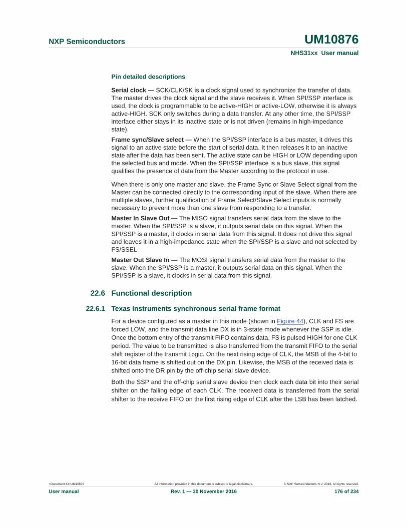
<Document ID>UM10876 All information provided in this document is subject to legal disclaimers. © NXP Semiconductors N.V. 2016. All rights reserved.
User manual Rev. 1 — 30 November 2016 176 of 234
NXP Semiconductors UM10876NHS31xx User manual
Pin detailed descriptions
Serial clock — SCK/CLK/SK is a clock signal used to synchronize the transfer of data. The master drives the clock signal and the slave receives it. When SPI/SSP interface is used, the clock is programmable to be active-HIGH or active-LOW, otherwise it is always active-HIGH. SCK only switches during a data transfer. At any other time, the SPI/SSP interface either stays in its inactive state or is not driven (remains in high-impedance state).Frame sync/Slave select — When the SPI/SSP interface is a bus master, it drives this signal to an active state before the start of serial data. It then releases it to an inactive state after the data has been sent. The active state can be HIGH or LOW depending upon the selected bus and mode. When the SPI/SSP interface is a bus slave, this signal qualifies the presence of data from the Master according to the protocol in use.
When there is only one master and slave, the Frame Sync or Slave Select signal from the Master can be connected directly to the corresponding input of the slave. When there are multiple slaves, further qualification of Frame Select/Slave Select inputs is normally necessary to prevent more than one slave from responding to a transfer.Master In Slave Out — The MISO signal transfers serial data from the slave to the master. When the SPI/SSP is a slave, it outputs serial data on this signal. When the SPI/SSP is a master, it clocks in serial data from this signal. It does not drive this signal and leaves it in a high-impedance state when the SPI/SSP is a slave and not selected by FS/SSELMaster Out Slave In — The MOSI signal transfers serial data from the master to the slave. When the SPI/SSP is a master, it outputs serial data on this signal. When the SPI/SSP is a slave, it clocks in serial data from this signal.
22.6 Functional description
22.6.1 Texas Instruments synchronous serial frame format
For a device configured as a master in this mode (shown in Figure 44), CLK and FS are forced LOW, and the transmit data line DX is in 3-state mode whenever the SSP is idle. Once the bottom entry of the transmit FIFO contains data, FS is pulsed HIGH for one CLK period. The value to be transmitted is also transferred from the transmit FIFO to the serial shift register of the transmit Logic. On the next rising edge of CLK, the MSB of the 4-bit to 16-bit data frame is shifted out on the DX pin. Likewise, the MSB of the received data is shifted onto the DR pin by the off-chip serial slave device.
Both the SSP and the off-chip serial slave device then clock each data bit into their serialshifter on the falling edge of each CLK. The received data is transferred from the serialshifter to the receive FIFO on the first rising edge of CLK after the LSB has been latched.
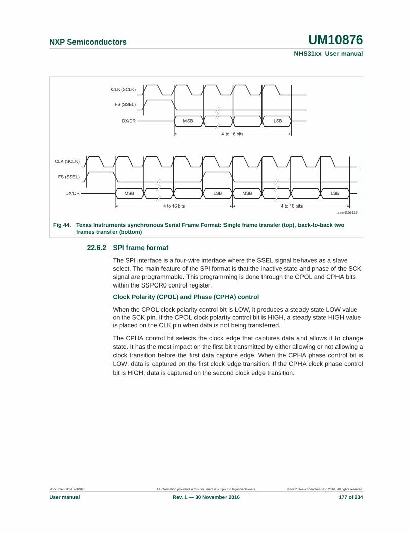
<Document ID>UM10876 All information provided in this document is subject to legal disclaimers. © NXP Semiconductors N.V. 2016. All rights reserved.
User manual Rev. 1 — 30 November 2016 177 of 234
NXP Semiconductors UM10876NHS31xx User manual
22.6.2 SPI frame format
The SPI interface is a four-wire interface where the SSEL signal behaves as a slave select. The main feature of the SPI format is that the inactive state and phase of the SCK signal are programmable. This programming is done through the CPOL and CPHA bits within the SSPCR0 control register.
Clock Polarity (CPOL) and Phase (CPHA) control
When the CPOL clock polarity control bit is LOW, it produces a steady state LOW value on the SCK pin. If the CPOL clock polarity control bit is HIGH, a steady state HIGH value is placed on the CLK pin when data is not being transferred.
The CPHA control bit selects the clock edge that captures data and allows it to changestate. It has the most impact on the first bit transmitted by either allowing or not allowing aclock transition before the first data capture edge. When the CPHA phase control bit isLOW, data is captured on the first clock edge transition. If the CPHA clock phase controlbit is HIGH, data is captured on the second clock edge transition.
Fig 44. Texas Instruments synchronous Serial Frame Format: Single frame transfer (top), back-to-back two frames transfer (bottom)
aaa-016499
MSB
MSB
CLK (SCLK)
FS (SSEL)
DX/DR
CLK (SCLK)
FS (SSEL)
DX/DR
LSB LSBMSB
4 to 16 bits
LSB
4 to 16 bits 4 to 16 bits

<Document ID>UM10876 All information provided in this document is subject to legal disclaimers. © NXP Semiconductors N.V. 2016. All rights reserved.
User manual Rev. 1 — 30 November 2016 178 of 234
NXP Semiconductors UM10876NHS31xx User manual
SPI format with CPOL = logic 0, CPHA = logic 0
Single and continuous transmission signal sequences for SPI format with CPOL = logic 0, CPHA = logic 0 are shown in Figure 46.
In this configuration, during idle periods:
• The CLK signal is forced LOW
Fig 45. SPI bus timing
D6 D5 D4 D3D7 D2 D1 D0
aaa-016972
SCK (CPOL = 0, CPHA = 0)
SCK (CPOL = 1, CPHA = 0)
SCK (CPOL = 1, CPHA = 1)
SCK (CPOL = 0, CPHA = 1)
IO
Fig 46. SPI frame format with CPOL = logic 0 and CPHA = logic 0. (a) Single and b) Continuous Transfer
SCKSSEL
MISO
a. Single transfer with CPOL = 0 and CPHA = 0
b. Continuous transfer with CPOL = 0 and CPHA = 0 aaa-022476
MOSIMSB LSB
LSB
4 to 16 bits
QMSB
SCKSSEL
MISO
MOSI MSB LSB
LSB
4 to 16 bits
QMSB
MSB LSB
LSB
4 to 16 bits
QMSB
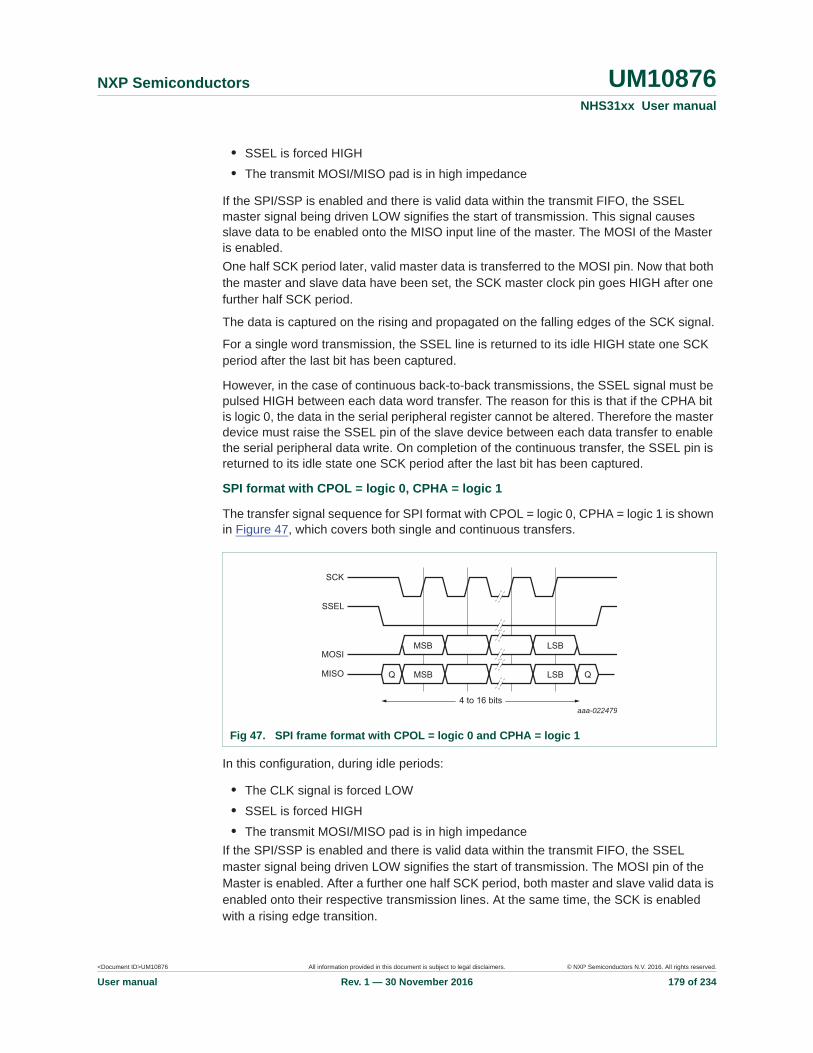
<Document ID>UM10876 All information provided in this document is subject to legal disclaimers. © NXP Semiconductors N.V. 2016. All rights reserved.
User manual Rev. 1 — 30 November 2016 179 of 234
NXP Semiconductors UM10876NHS31xx User manual
• SSEL is forced HIGH• The transmit MOSI/MISO pad is in high impedance
If the SPI/SSP is enabled and there is valid data within the transmit FIFO, the SSEL master signal being driven LOW signifies the start of transmission. This signal causes slave data to be enabled onto the MISO input line of the master. The MOSI of the Master is enabled.One half SCK period later, valid master data is transferred to the MOSI pin. Now that both the master and slave data have been set, the SCK master clock pin goes HIGH after one further half SCK period.
The data is captured on the rising and propagated on the falling edges of the SCK signal.
For a single word transmission, the SSEL line is returned to its idle HIGH state one SCK period after the last bit has been captured.
However, in the case of continuous back-to-back transmissions, the SSEL signal must be pulsed HIGH between each data word transfer. The reason for this is that if the CPHA bit is logic 0, the data in the serial peripheral register cannot be altered. Therefore the master device must raise the SSEL pin of the slave device between each data transfer to enable the serial peripheral data write. On completion of the continuous transfer, the SSEL pin is returned to its idle state one SCK period after the last bit has been captured.
SPI format with CPOL = logic 0, CPHA = logic 1
The transfer signal sequence for SPI format with CPOL = logic 0, CPHA = logic 1 is shown in Figure 47, which covers both single and continuous transfers.
In this configuration, during idle periods:
• The CLK signal is forced LOW• SSEL is forced HIGH• The transmit MOSI/MISO pad is in high impedance
If the SPI/SSP is enabled and there is valid data within the transmit FIFO, the SSEL master signal being driven LOW signifies the start of transmission. The MOSI pin of the Master is enabled. After a further one half SCK period, both master and slave valid data is enabled onto their respective transmission lines. At the same time, the SCK is enabled with a rising edge transition.
Fig 47. SPI frame format with CPOL = logic 0 and CPHA = logic 1
SCK
SSEL
MISO
aaa-022479
MOSIMSB LSB
LSB
4 to 16 bits
QMSBQ
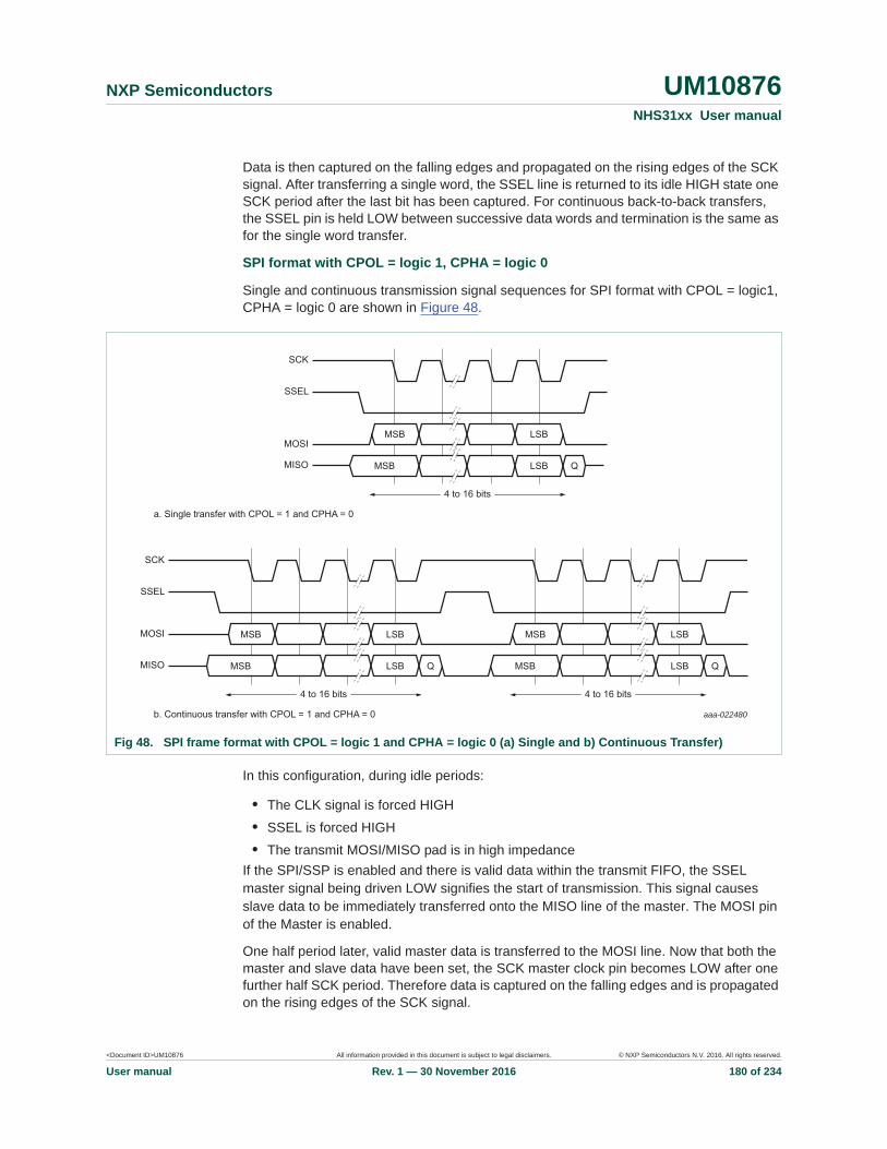
<Document ID>UM10876 All information provided in this document is subject to legal disclaimers. © NXP Semiconductors N.V. 2016. All rights reserved.
User manual Rev. 1 — 30 November 2016 180 of 234
NXP Semiconductors UM10876NHS31xx User manual
Data is then captured on the falling edges and propagated on the rising edges of the SCK signal. After transferring a single word, the SSEL line is returned to its idle HIGH state one SCK period after the last bit has been captured. For continuous back-to-back transfers, the SSEL pin is held LOW between successive data words and termination is the same as for the single word transfer.
SPI format with CPOL = logic 1, CPHA = logic 0
Single and continuous transmission signal sequences for SPI format with CPOL = logic1, CPHA = logic 0 are shown in Figure 48.
In this configuration, during idle periods:
• The CLK signal is forced HIGH• SSEL is forced HIGH• The transmit MOSI/MISO pad is in high impedance
If the SPI/SSP is enabled and there is valid data within the transmit FIFO, the SSEL master signal being driven LOW signifies the start of transmission. This signal causes slave data to be immediately transferred onto the MISO line of the master. The MOSI pin of the Master is enabled.
One half period later, valid master data is transferred to the MOSI line. Now that both the master and slave data have been set, the SCK master clock pin becomes LOW after one further half SCK period. Therefore data is captured on the falling edges and is propagated on the rising edges of the SCK signal.
Fig 48. SPI frame format with CPOL = logic 1 and CPHA = logic 0 (a) Single and b) Continuous Transfer)
SSEL
MISO
a. Single transfer with CPOL = 1 and CPHA = 0
b. Continuous transfer with CPOL = 1 and CPHA = 0 aaa-022480
MOSIMSB LSB
LSB
4 to 16 bits
QMSB
SCK
SSEL
MISO
MOSI MSB LSB
LSB
4 to 16 bits
QMSB
MSB LSB
LSB
4 to 16 bits
QMSB
SCK

<Document ID>UM10876 All information provided in this document is subject to legal disclaimers. © NXP Semiconductors N.V. 2016. All rights reserved.
User manual Rev. 1 — 30 November 2016 181 of 234
NXP Semiconductors UM10876NHS31xx User manual
For a single word transmission: After all bits have been transferred, the SSEL line is returned to its idle HIGH state one SCK period after the last bit has been captured.
However, in the case of continuous back-to-back transmissions, the SSEL signal must be pulsed HIGH between each data word transfer. The reason for this is that if the CPHA bit is logic 0, the data in the serial peripheral register cannot be altered. Therefore the master device must raise the SSEL pin of the slave device between each data transfer to enable the serial peripheral data write. On completion of the continuous transfer, the SSEL pin is returned to its idle state one SCK period after the last bit has been captured.
SPI format with CPOL = logic 1, CPHA = logic 1
The transfer signal sequence for SPI format with CPOL = logic 1, CPHA = logic1 is shown in Figure 49, which covers both single and continuous transfers.
In this configuration, during idle periods:
• The CLK signal is forced HIGH• SSEL is forced HIGH• The transmit MOSI/MISO pad is in high impedance
If the SPI/SSP is enabled and there is valid data within the transmit FIFO, the SSEL master signal being driven LOW signifies the start of transmission. The MOSI pin of the Master is enabled. After a further one half SCK period, both master and slave data are enabled into their respective transmission lines. At the same time, the SCK is enabled with a falling edge transition. Data is then captured on the rising edges and propagated on the falling edges of the SCK signal.
In the case of a single word transmission: After all bits have been transferred, the SSEL line is returned to its idle HIGH state one SCK period after the last bit has been captured.
For continuous back-to-back transmissions: The SSEL pins remain in their active LOW state until the final bit of the last word has been captured. They then return to their idle state as described above.
Generally, for continuous back-to-back transfers, the SSEL pin is held LOW between successive data words and termination is the same as for a single word transfer.
Fig 49. SPI frame format with CPOL = logic 1 and CPHA = logic 1
SSEL
MISO
aaa-022481
MOSIMSB LSB
LSB
4 to 16 bits
QMSBQ
SCK
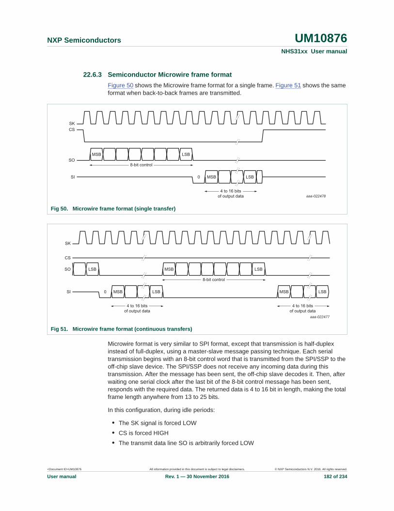
<Document ID>UM10876 All information provided in this document is subject to legal disclaimers. © NXP Semiconductors N.V. 2016. All rights reserved.
User manual Rev. 1 — 30 November 2016 182 of 234
NXP Semiconductors UM10876NHS31xx User manual
22.6.3 Semiconductor Microwire frame formatFigure 50 shows the Microwire frame format for a single frame. Figure 51 shows the same format when back-to-back frames are transmitted.
Microwire format is very similar to SPI format, except that transmission is half-duplex instead of full-duplex, using a master-slave message passing technique. Each serial transmission begins with an 8-bit control word that is transmitted from the SPI/SSP to the off-chip slave device. The SPI/SSP does not receive any incoming data during this transmission. After the message has been sent, the off-chip slave decodes it. Then, after waiting one serial clock after the last bit of the 8-bit control message has been sent, responds with the required data. The returned data is 4 to 16 bit in length, making the total frame length anywhere from 13 to 25 bits.
In this configuration, during idle periods:
• The SK signal is forced LOW• CS is forced HIGH• The transmit data line SO is arbitrarily forced LOW
Fig 50. Microwire frame format (single transfer)
aaa-022478
SK
MSB
SI MSB
LSB
4 to 16 bitsof output data
CS
SO8-bit control
LSB0
Fig 51. Microwire frame format (continuous transfers)
aaa-022477
SK
CS
SO LSB MSB
SI MSB
LSB
4 to 16 bitsof output data
4 to 16 bitsof output data
8-bit control
LSB MSB LSB0
<Document ID>UM10876 All information provided in this document is subject to legal disclaimers. © NXP Semiconductors N.V. 2016. All rights reserved.
User manual Rev. 1 — 30 November 2016 183 of 234
NXP Semiconductors UM10876NHS31xx User manual
A transmission is triggered by writing a control byte to the transmit FIFO. The falling edge of CS causes the bottom entry value of the transmit FIFO to be transferred to the serial shift register of the transmit logic. It also causes the MSB of the 8-bit control frame to be shifted out onto the SO pin. CS remains LOW during the frame transmission. The SI pin remains in 3-state during this transmission. The off-chip serial slave device latches each control bit into its serial shifter on the rising edge of each SK. After the slave device latches the last bit, the control byte is decoded during a one clock wait state. The slave responds by transmitting data back to the SPI/SSP. Each bit is driven onto SI line on the falling edge of SK. The SPI/SSP in turn latches each bit on the rising edge of SK. At the end of the frame, for single transfers, the CS signal is pulled HIGH one clock period after the last bit has been latched in the receive serial shifter. This signal causes the data to be transferred to the receive FIFO.
Note: The off-chip slave device can 3-state the receive line either on the falling edge of SK after the receive shifter latches the LSB, or when the CS pin goes HIGH.
For continuous transfers, data transmission begins and ends in the same manner as a single transfer. However, the CS line is continuously asserted (held LOW) and transmission of data occurs back to back. The control byte of the next frame follows directly after the LSB of the received data from the current frame. Each received value is transferred from the receive shifter on the falling edge SK, after the LSB of the frame has been latched into the SPI/SSP.
22.7 Register descriptions The register addresses of the SPI controllers are shown in Table 241.
The reset values reflect the data stored in used bits only, it does not include the content of reserved bits.
22.7.1 SPI/SSP Control register 0 (CR0)This register controls the basic operation of the SPI/SSP controller.
Always write settings to this register, even if the desired settings match the reset default.
Table 241. Register overview: Serial Peripheral Interface (base address 0x4004 0000)Name Access Address
offsetDescription Reset value
CR0 RW 0x000 Control Register logic 0. Selects the serial clock rate, bus type, and data size
0x0000 000F
CR1 RW 0x004 Control Register logic 1. Selects master/slave and other modes 0x0000 0000
DR RW 0x008 data Register. Writes fill the transmit FIFO, and reads empty the receive FIFO
0x0000 0000
SR R 0x00C Status Register 0x0000 0003
CPSR RW 0x010 Clock Prescale Register 0x0000 0000
IMSC RW 0x014 Interrupt Mask Set and Clear register 0x0000 0000
RIS R 0x018 Raw Interrupt Status register 0x0000 0008
MIS R 0x01C Masked Interrupt Status register 0x0000 0000
ICR W 0x020 Interrupt Clear Register n/a
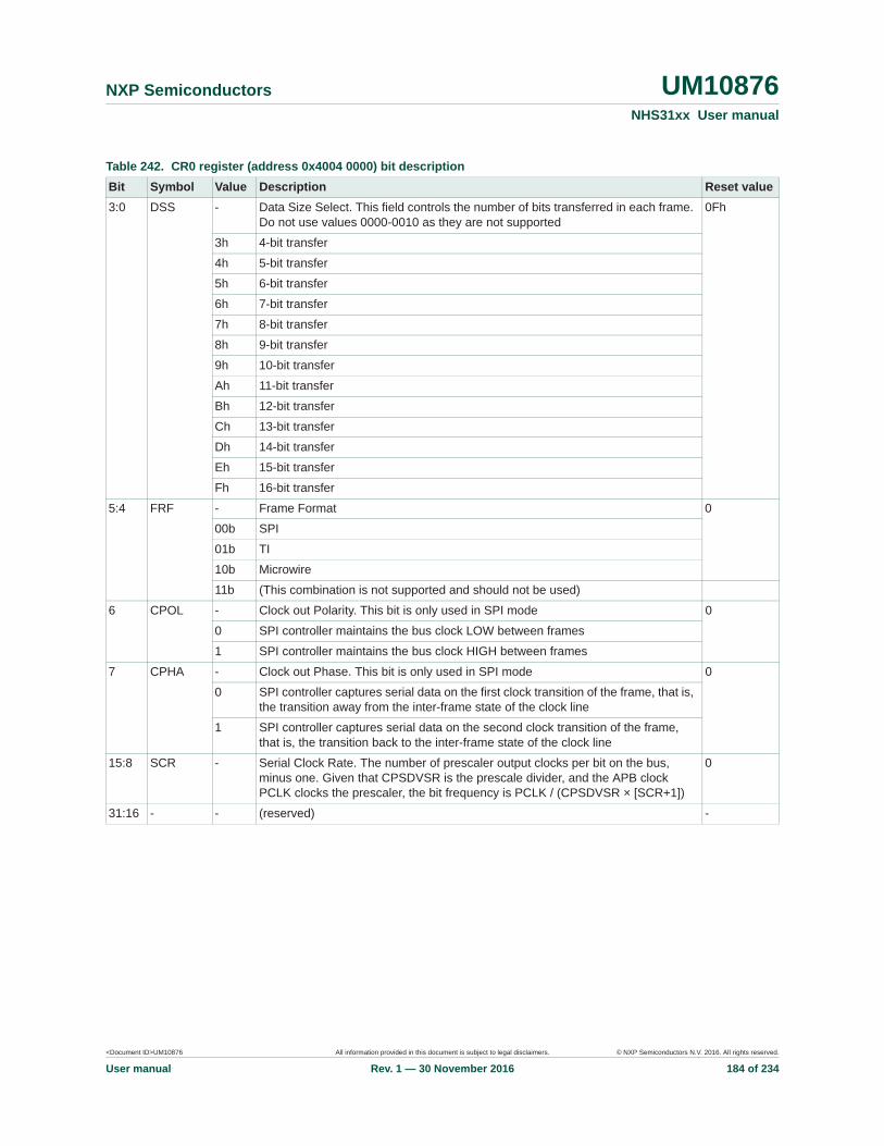
<Document ID>UM10876 All information provided in this document is subject to legal disclaimers. © NXP Semiconductors N.V. 2016. All rights reserved.
User manual Rev. 1 — 30 November 2016 184 of 234
NXP Semiconductors UM10876NHS31xx User manual
Table 242. CR0 register (address 0x4004 0000) bit descriptionBit Symbol Value Description Reset value3:0 DSS - Data Size Select. This field controls the number of bits transferred in each frame.
Do not use values 0000-0010 as they are not supported0Fh
3h 4-bit transfer
4h 5-bit transfer
5h 6-bit transfer
6h 7-bit transfer
7h 8-bit transfer
8h 9-bit transfer
9h 10-bit transfer
Ah 11-bit transfer
Bh 12-bit transfer
Ch 13-bit transfer
Dh 14-bit transfer
Eh 15-bit transfer
Fh 16-bit transfer
5:4 FRF - Frame Format 0
00b SPI
01b TI
10b Microwire
11b (This combination is not supported and should not be used)
6 CPOL - Clock out Polarity. This bit is only used in SPI mode 0
0 SPI controller maintains the bus clock LOW between frames
1 SPI controller maintains the bus clock HIGH between frames
7 CPHA - Clock out Phase. This bit is only used in SPI mode 0
0 SPI controller captures serial data on the first clock transition of the frame, that is, the transition away from the inter-frame state of the clock line
1 SPI controller captures serial data on the second clock transition of the frame, that is, the transition back to the inter-frame state of the clock line
15:8 SCR - Serial Clock Rate. The number of prescaler output clocks per bit on the bus, minus one. Given that CPSDVSR is the prescale divider, and the APB clock PCLK clocks the prescaler, the bit frequency is PCLK / (CPSDVSR × [SCR+1])
0
31:16 - - (reserved) -
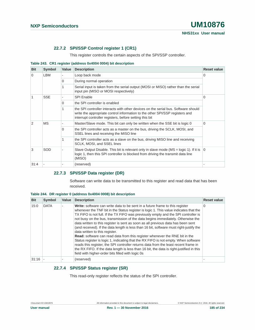
<Document ID>UM10876 All information provided in this document is subject to legal disclaimers. © NXP Semiconductors N.V. 2016. All rights reserved.
User manual Rev. 1 — 30 November 2016 185 of 234
NXP Semiconductors UM10876NHS31xx User manual
22.7.2 SPI/SSP Control register 1 (CR1)This register controls the certain aspects of the SPI/SSP controller.
22.7.3 SPI/SSP Data register (DR)
Software can write data to be transmitted to this register and read data that has been received.
22.7.4 SPI/SSP Status register (SR)
This read-only register reflects the status of the SPI controller.
Table 243. CR1 register (address 0x4004 0004) bit descriptionBit Symbol Value Description Reset value0 LBM - Loop back mode 0
0 During normal operation
1 Serial input is taken from the serial output (MOSI or MISO) rather than the serial input pin (MISO or MOSI respectively)
1 SSE - SPI Enable 0
0 the SPI controller is enabled
1 the SPI controller interacts with other devices on the serial bus. Software should write the appropriate control information to the other SPI/SSP registers and interrupt controller registers, before setting this bit
2 MS - Master/Slave mode. This bit can only be written when the SSE bit is logic 0 0
0 the SPI controller acts as a master on the bus, driving the SCLK, MOSI, and SSEL lines and receiving the MISO line
1 the SPI controller acts as a slave on the bus, driving MISO line and receiving SCLK, MOSI, and SSEL lines
3 SOD - Slave Output Disable. This bit is relevant only in slave mode (MS = logic 1). If it is logic 1, then this SPI controller is blocked from driving the transmit data line (MISO)
0
31:4 - - (reserved) -
Table 244. DR register 0 (address 0x4004 0008) bit descriptionBit Symbol Value Description Reset value15:0 DATA - Write: software can write data to be sent in a future frame to this register
whenever the TNF bit in the Status register is logic 1. This value indicates that the TX FIFO is not full. If the TX FIFO was previously empty and the SPI controller is not busy on the bus, transmission of the data begins immediately. Otherwise the data written to this register is sent as soon as all previous data has been sent (and received). If the data length is less than 16 bit, software must right-justify the data written to this register.Read: software can read data from this register whenever the RNE bit in the Status register is logic 1, indicating that the RX FIFO is not empty. When software reads this register, the SPI controller returns data from the least recent frame in the RX FIFO. If the data length is less than 16 bit, the data is right-justified in this field with higher-order bits filled with logic 0s
0
31:16 - - (reserved) -

<Document ID>UM10876 All information provided in this document is subject to legal disclaimers. © NXP Semiconductors N.V. 2016. All rights reserved.
User manual Rev. 1 — 30 November 2016 186 of 234
NXP Semiconductors UM10876NHS31xx User manual
22.7.5 SPI/SSP clock Prescale register (CPSR)
This register controls the factor by which the prescaler divides the SPI peripheral clock SPI_PCLK to yield the prescaler clock. The prescaler clock is, in turn, divided by the SCR factor in the SSPCR0 registers to determine the bit clock.
22.7.6 SPI/SSP Interrupt Mask Set/Clear Register (IMSC)This register controls whether each of the four possible interrupt conditions in the SPI controller are enabled. Note: ARM uses the word ’masked’ in the opposite sense from classic computer terminology, in which ’masked’ meant ’disabled’. ARM uses the word ’masked’ to mean ’enabled’. To avoid confusion, we avoid using the word ’masked’.
22.7.7 SPI/SSP Raw interrupt status register (RIS)
This read-only register contains a logic 1 for each interrupt condition that is asserted, regardless of whether the interrupt is enabled in the SSPIMSC registers.
Table 245. SR register (address 0x4004 000C) bit description Bit Symbol Value Description Reset value0 TFE - Transmit FIFO Empty. This bit is logic 1 if the Transmit FIFO is empty, logic 0 if
not1
1 TNF - Transmit FIFO Not Full. This bit is logic 0 if the TX FIFO is full, logic 1 if not 1
2 RNE - Receive FIFO Not Empty. This bit is logic 0 if the Receive FIFO is empty, logic 1 if not
0
3 RFF - Receive FIFO Full. This bit is logic 1 if the Receive FIFO is full, logic 0 if not 0
4 BSY - Busy. This bit is logic 0 if the SPI controller is idle, logic 1 if it is sending/receiving a frame and/or the TX FIFO is not empty
0
31:5 - - (reserved) -
Table 246. CPSR register (address 0x4004 0010) bit descriptionBit Symbol Value Description Reset value7:0 CPSDVSR - this even value between 2 and 254, by which SPI_PCLK is divided to yield the
prescaler output clock. Bit 0 always reads as logic 00
31:8 - - (reserved) -
Table 247. IMSC register (address 0x4004 0014) bit descriptionBit Symbol Value Description Reset value0 RORIM - software should set this bit to enable interrupt when a Receive Overrun occurs.
That is, when the RX FIFO is full and another frame is received. The ARM spec implies that the preceding frame data is overwritten by the new frame data in this instance
0
1 RTIM - software should set this bit to enable interrupt when a Receive Time-out condition occurs. A Receive Time-out occurs when the RX FIFO is not empty, and no has not been read for a timeout period. The SSP bit rate determines the timeout period, which is the same for master and slave modes: 32 bits at PCLK / (CPSDVSR [SCR+1])
0
2 RXIM - software should set this bit to enable interrupt when the RX FIFO is at least half full
0
3 TXIM - software should set this bit to enable interrupt when the TX FIFO is at least half empty
0
31:54 - - (reserved) -
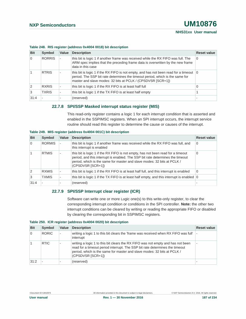
<Document ID>UM10876 All information provided in this document is subject to legal disclaimers. © NXP Semiconductors N.V. 2016. All rights reserved.
User manual Rev. 1 — 30 November 2016 187 of 234
NXP Semiconductors UM10876NHS31xx User manual
22.7.8 SPI/SSP Masked interrupt status register (MIS)
This read-only register contains a logic 1 for each interrupt condition that is asserted and enabled in the SSPIMSC registers. When an SPI interrupt occurs, the interrupt service routine should read this register to determine the cause or causes of the interrupt.
22.7.9 SPI/SSP Interrupt clear register (ICR)
Software can write one or more Logic one(s) to this write-only register, to clear the corresponding interrupt condition or conditions in the SPI controller. Note: the other two interrupt conditions can be cleared by writing or reading the appropriate FIFO or disabled by clearing the corresponding bit in SSPIMSC registers.
Table 248. RIS register (address 0x4004 0018) bit descriptionBit Symbol Value Description Reset value0 RORRIS - this bit is logic 1 if another frame was received while the RX FIFO was full. The
ARM spec implies that the preceding frame data is overwritten by the new frame data in this case
0
1 RTRIS - this bit is logic 1 if the RX FIFO is not empty, and has not been read for a timeout period. The SSP bit rate determines the timeout period, which is the same for master and slave modes: 32 bits at PCLK / (CPSDVSR [SCR+1])
0
2 RXRIS - this bit is logic 1 if the RX FIFO is at least half full 0
3 TXRIS - this bit is logic 1 if the TX FIFO is at least half empty 1
31:4 - - (reserved) -
Table 249. MIS register (address 0x4004 001C) bit descriptionBit Symbol Value Description Reset value0 RORMIS - this bit is logic 1 if another frame was received while the RX FIFO was full, and
this interrupt is enabled0
1 RTMIS - this bit is logic 1 if the RX FIFO is not empty, has not been read for a timeout period, and this interrupt is enabled. The SSP bit rate determines the timeout period, which is the same for master and slave modes: 32 bits at PCLK / (CPSDVSR [SCR+1])
0
2 RXMIS - this bit is logic 1 if the RX FIFO is at least half full, and this interrupt is enabled 0
3 TXMIS - this bit is logic 1 if the TX FIFO is at least half empty, and this interrupt is enabled 0
31:4 - - (reserved) -
Table 250. ICR register (address 0x4004 0020) bit descriptionBit Symbol Value Description Reset value0 RORIC - writing a logic 1 to this bit clears the ’frame was received when RX FIFO was full’
interrupt-
1 RTIC - writing a logic 1 to this bit clears the RX FIFO was not empty and has not been read for a timeout period interrupt. The SSP bit rate determines the timeout period, which is the same for master and slave modes: 32 bits at PCLK / (CPSDVSR [SCR+1])
-
31:2 - - (reserved) -

<Document ID>UM10876 All information provided in this document is subject to legal disclaimers. © NXP Semiconductors N.V. 2016. All rights reserved.
User manual Rev. 1 — 30 November 2016 188 of 234
NXP Semiconductors UM10876NHS31xx User manual
23. General-Purpose Input Output (GPIO)
23.1 About this chapterThis chapter describes the GPIO (AHB 0x5000 0000).
23.2 Features
• GPIO pins can be configured as input or output by software• Each individual port pin can serve as an edge or level-sensitive interrupt request• Interrupts can be configured on single falling or rising edges and on both edges• Level-sensitive interrupt pins can be HIGH or LOW-active• All GPIO pins are inputs by default• Address bits 13:2 mask the Reading and writing of GPIODATA registers
23.3 General descriptionEach GPIO register can be up to 12 bits wide and can be read or written using word or halfword operations at word addresses.
The reset values reflect the data stored in used bits only, it does not include the content of reserved bits.
23.4 Register description
Table 251. Register overview: General Purpose I/O (base address 0x5000 0000)Name Access Address
offsetDescription Reset value
GPIODATA RW 0x0000 -0x3FF8
data address masking register locations for pins PIO0_0 to PIO0_11 n/a
GPIODATA RW 0x3FFC data register for pins PIO_0 to PIO0_11 n/a
- - 0x4000 -0x7FFC
(reserved) -
DIR RW 0x8000 data direction register 0x0000 0000
IS RW 0x8004 interrupt sense register 0x0000 0000
IBE RW 0x8008 interrupt both edges register 0x0000 0000
IEV RW 0x800C interrupt event register 0x0000 0000
IMSC RW 0x8010 interrupt mask register 0x0000 0000
RIS R 0x8014 raw interrupt status register 0x0000 0000
MIS R 0x8018 masked interrupt status register 0x0000 0000
IC W 0x801C interrupt clear register 0x0000 0000
- - 0x8020 -0xFFFF
(reserved) -
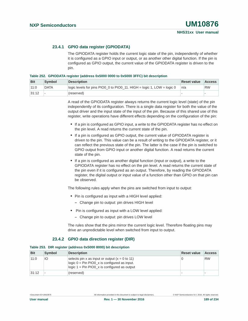
<Document ID>UM10876 All information provided in this document is subject to legal disclaimers. © NXP Semiconductors N.V. 2016. All rights reserved.
User manual Rev. 1 — 30 November 2016 189 of 234
NXP Semiconductors UM10876NHS31xx User manual
23.4.1 GPIO data register (GPIODATA)The GPIODATA register holds the current logic state of the pin, independently of whether it is configured as a GPIO input or output, or as another other digital function. If the pin is configured as GPIO output, the current value of the GPIODATA register is driven to the pin.
A read of the GPIODATA register always returns the current logic level (state) of the pin independently of its configuration. There is a single data register for both the value of the output driver and the input state of the input of the pin. Because of this shared use of this register, write operations have different effects depending on the configuration of the pin:
• If a pin is configured as GPIO input, a write to the GPIODATA register has no effect on the pin level. A read returns the current state of the pin.
• If a pin is configured as GPIO output, the current value of GPIODATA register is driven to the pin. This value can be a result of writing to the GPIODATA register, or it can reflect the previous state of the pin. The latter is the case if the pin is switched to GPIO output from GPIO input or another digital function. A read returns the current state of the pin.
• If a pin is configured as another digital function (input or output), a write to the GPIODATA register has no effect on the pin level. A read returns the current state of the pin even if it is configured as an output. Therefore, by reading the GPIODATA register, the digital output or input value of a function other than GPIO on that pin can be observed.
The following rules apply when the pins are switched from input to output:
• Pin is configured as input with a HIGH level applied:– Change pin to output: pin drives HIGH level
• Pin is configured as input with a LOW level applied:– Change pin to output: pin drives LOW level
The rules show that the pins mirror the current logic level. Therefore floating pins may drive an unpredictable level when switched from input to output.
23.4.2 GPIO data direction register (DIR)
Table 252. GPIODATA register (address 0x5000 0000 to 0x5000 3FFC) bit descriptionBit Symbol Description Reset value Access11:0 DATA logic levels for pins PIO0_0 to PIO0_11. HIGH = logic 1, LOW = logic 0 n/a RW
31:12 - (reserved) - -
Table 253. DIR register (address 0x5000 8000) bit descriptionBit Symbol Description Reset value Access11:0 IO selects pin x as input or output (x = 0 to 11)
logic 0 = Pin PIO0_x is configured as input.logic 1 = Pin PIO0_x is configured as output
0 RW
31:12 - (reserved) - -
<Document ID>UM10876 All information provided in this document is subject to legal disclaimers. © NXP Semiconductors N.V. 2016. All rights reserved.
User manual Rev. 1 — 30 November 2016 190 of 234
NXP Semiconductors UM10876NHS31xx User manual
23.4.3 GPIO interrupt sense register (IS)
23.4.4 GPIO interrupt both edges sense register (IBE)
23.4.5 GPIO interrupt event register (IEV)
23.4.6 GPIO interrupt mask register (IMSC)Bits set to HIGH in the IMSC register allow the corresponding pins to trigger their individual interrupts and the combined GPIO interrupt line. Clearing a bit disables interrupt triggering on that pin.
23.4.7 GPIO raw interrupt status register (RIS)Bits read HIGH in the RIS register reflect the raw (prior to masking) interrupt status of the corresponding pins. This status indicates that all the requirements have been met before they are allowed to trigger the IMSC. Bits read as zero indicate that the corresponding input pins have not initiated an interrupt. The register is read-only.
Table 254. IS register (address 0x5000 8004) bit descriptionBit Symbol Description Reset value Access11:0 ISENSE selects interrupt on pin x as level or edge sensitive (x = 0 to 11)
logic 0 = Interrupt on pin PIO0_x is configured as edge sensitivelogic 1 = Interrupt on pin PIO0_x is configured as level sensitive
0 RW
31:12 - (reserved) 0 -
Table 255. IBE register (address 0x5000 8008) bit descriptionBit Symbol Description Reset value Access11:0 IBE selects interrupt on pin x as level or edge sensitive (x = 0 to 11).
logic 0 = Interrupt on pin PIO0_x is controlled through register GPIOIEVlogic 1 = Both edges on pin PIO0_x trigger an interrupt
0 RW
31:12 - (reserved) 0 -
Table 256. IEV register (address 0x5000 800C) bit descriptionBit Symbol Description Reset value Access11:0 IEV selects interrupt on pin x to be triggered rising or falling edges (x = 0 to
11).logic 0 = Depending on setting in register IS, falling edges or LOW level on pin PIO0_x trigger an interruptlogic 1 = Depending on setting in register IS, rising edges or HIGH level on pin PIO0_x trigger an interrupt
0 RW
31:12 - (reserved) 0 -
Table 257. IMSC register (address 0x5000 8010) bit descriptionBit Symbol Description Reset value Access11:0 MASK selects interrupt on pin x to be masked (x = 0 to 11).
logic 0 = Interrupt on pin PIO0_x is masked.logic 1 = Interrupt on pin PIO0_x is not masked
0 RW
31:12 - (reserved) 0 -
<Document ID>UM10876 All information provided in this document is subject to legal disclaimers. © NXP Semiconductors N.V. 2016. All rights reserved.
User manual Rev. 1 — 30 November 2016 191 of 234
NXP Semiconductors UM10876NHS31xx User manual
23.4.8 GPIO masked interrupt status register (MIS)Bits read HIGH in the MIS register reflect the status of the input lines triggering an interrupt. Bits read as LOW indicate that either no interrupt on the corresponding input pins has been generated or that the interrupt is masked. MIS is the state of the interrupt after masking. The register is read-only.
23.4.9 GPIO interrupt clear register (IC)This register allows software to clear edge detection for port bits that are identified as edge-sensitive in the interrupt Sense register. This register has no effect on port bits identified as level sensitive.
23.5 Functional description
23.5.1 Write/read data operationBits [13:2] of a 14-bit wide address bus are used to create a 12-bit wide mask for write and read operations on the 12 GPIO pins for each port. This mask enables software to set GPIO bits without affecting any other pins in a single write operation: Read and write operations only affect GPIODATA bits masked by logic 1.
The masked GPIODATA register can be located anywhere between address offsets 0x0000 to 0x3FFC in the GPIO address space. Reading and writing to the GPIODATA register at address 0x3FFC sets all masking bits to logic 1.
Write operation
Table 258. RIS register (address 0x5000 8014) bit descriptionBit Symbol Description Reset value Access11:0 RAWST raw interrupt status (x = 0 to 11).
logic 0 = No interrupt on pin PIO0_x.logic 1 = Interrupt requirements met on PIO0_x
0 RW
31:12 - (reserved) 0 -
Table 259. MIS register (address 0x5000 8018) bit descriptionBit Symbol Description Reset value Access11:0 MASK selects interrupt on pin x to be masked (x = 0 to 11).
logic 0 = No interrupt or interrupt masked on pin PIO0_x.logic 1 = Interrupt on PIO0_x
0 R
31:12 - (reserved) 0 -
Table 260. IC register (address 0x5000 801C) bit descriptionBit Symbol Description Reset value Access11:0 CLR selects interrupt on pin x to be cleared (x = 0 to 11). Clears the interrupt
edge detection logic. This register is write-only.Remark: The synchronizer between the GPIO and the NVIC blocks causes a delay of 2 clocks. Two NOPs should be added after the clear of the interrupt edge detection logic before the exit of the interrupt service routine.logic 0 = No effect.logic 1 = Clears edge detection logic for pin PIO0_x
0 W
31:12 - (reserved) 0 -
<Document ID>UM10876 All information provided in this document is subject to legal disclaimers. © NXP Semiconductors N.V. 2016. All rights reserved.
User manual Rev. 1 — 30 November 2016 192 of 234
NXP Semiconductors UM10876NHS31xx User manual
If address bit (i+2) associated with the GPIO port bit i (i = 0 to 11) to be written is HIGH, the GPIODATA register bit i is updated. If the address bit (i+2) is LOW, the corresponding GPIODATA register bit i is left unchanged.
Read operation
If the address bit associated with the GPIO data bit is HIGH, the value is read. If the address bit is LOW, the GPIO data bit is read as logic 0. Reading a port DATA register yields the state of port pins 11:0 ANDed with address bits 13:2.
Fig 52. Masked write operation to the GPIODATA register
Fig 53. Masked GPIO read operation
aaa-017855
0 0 0 0 0 0 1 0 0 1 1 0
1 1 1 1 1 1 1 0 0 1 0 0
u u u u u u 1 u u 1 0 u
0 0
13
address 0x098
data 0xFE4
GPIODATA registerat address + 0x098
ADDRESS[13:2] 12 11 10 9 8 7 6 5 4 3 2
u = unchanged
aaa-017856
0 0 0 0 0 0 1 1 0 0 0 1
1 1 1 1 1 1 1 0 0 1 0 0
0 0 0 0 0 0 1 0 0 0 0 0
0 0
13
address 0x0C4
port pin settings
data read
ADDRESS[13:2] 12 11 10 9 8 7 6 5 4 3 2

<Document ID>UM10876 All information provided in this document is subject to legal disclaimers. © NXP Semiconductors N.V. 2016. All rights reserved.
User manual Rev. 1 — 30 November 2016 193 of 234
NXP Semiconductors UM10876NHS31xx User manual
24. Input/Output configuration
24.1 About this chapterThis chapter describes the registers forming the Input/Output (IO) configuration block.
24.2 General descriptionThe I/O configuration registers control the electrical characteristics of the pads. The following features are programmable:
• pin function• internal pull-up/pull-down resistor or bus keeper function• low-pass filter• I2C-bus mode for pads hosting the I2C-bus function.
The IOCON registers control the function (GPIO or peripheral function), the input mode, and the hysteresis of all PIO_m pins. In addition, the I2C-bus pins can be configured for different I2C-bus modes.
24.2.1 PIO0 pin functionsThe FUNC bits in the IOCON registers can be set to GPIO (FUNC = 000) or to a peripheral function. If the pins are GPIO pins, the GPIO0DIR registers determine whether the pin is configured as an input or output. For any peripheral function, the pin direction is controlled automatically depending on the functionality of the pins. The GPIO0DIR registers have no effect on peripheral functions.
24.2.2 PIO0 pin modeThe MODE bits in the IOCON register allow the selection of on-chip pull-up or pull-down resistors for each pin, or to select the repeater mode. The possible on-chip resistor configurations are pull-up enabled, pull-down enabled, or no pull-up/pull-down. The default value is all disabled. The repeater mode enables the pull-up resistor when the pin is at logic 1, and enables the pull-down resistor when the pin is at logic 0. This mode causes the pin to retain its last known state, if it is configured as an input and is not driven externally. The state retention is not applicable to the Deep power-down mode. Repeater mode may typically be used to prevent a pin from floating when it is temporarily not driven. Allowing it to float could potentially use significant power.
The LPF bit indicates whether the low pass / glitch filtered input is selected or not.
Table 261. Pad direction and MFIO settingsDirection A (pad) NoteInput . Z input mode, externally driven
Output 0 0 output mode logic 0Output 1 1 output mode logic 1

<Document ID>UM10876 All information provided in this document is subject to legal disclaimers. © NXP Semiconductors N.V. 2016. All rights reserved.
User manual Rev. 1 — 30 November 2016 194 of 234
NXP Semiconductors UM10876NHS31xx User manual
24.2.3 PIO0 I2C modePads PIO0_4 and PIO0_5 can be used in I2C-bus and GPIO mode. The pads are open-drain (in both modes). The FUNC bits of registers IOCON_PIO0_4 and IOCON_PIO0_5 select the I2C-bus or GPIO mode. Depending on the selection, an input glitch filter is active or not:
• In I2C-bus mode (FUNC=001b), no glitch filter is present on the input but there is glitch filtering in the I2C-bus block
• In GPIO mode (FUNC=000b), a 50 ns glitch filter is active on the input
The I2CMODE bits of the registers IOCON_PIO0_4 and IOCON_PIO0_5 determine the output behavior, independent of the FUNC selection:
• With I2CMODE=00b (default), the selected mode is I2C-bus standard/fast mode transmit, with turn-on slew-rate control
• With I2CMODE=01b, the selected mode is open-drain GPIO (4 mA) without slew-rate control
The I2C-bus pads have no pull-up/pull down functionality.
24.2.4 PIO0 Current Drive modePIO0_3, PIO0_7, PIO0_10, and PIO0_11 are high-drive pads that can deliver up to 20 mA to the load. These PIO pins can be set to either digital mode or current sink mode. In digital mode, the output voltage of the pad switches between VSS and VDD. In current sink mode, the output current sink switches between Idrive(low) and Idrive(high) as set by the ILOW and IHI bits. The maximum pad voltage is limited to 5 V.
Table 262. LPF bit and MFIO pad output selectionLPF pad output selected0 ZI
1 ZIF
Table 263. Pad output behaviorRequested output from IC core
I2CMODE (pad) Mode
0 00 0 I2C-bus standard/fast mode transmit
1 00 Z I2C-bus standard/fast mode transmit
0 01 0 open-drain GPIO (4 mA)
1 01 Z open-drain GPIO (4 mA)
0 10 0 (reserved)
1 10 Z (reserved)
0 11 0 (reserved)
1 11 Z (reserved)
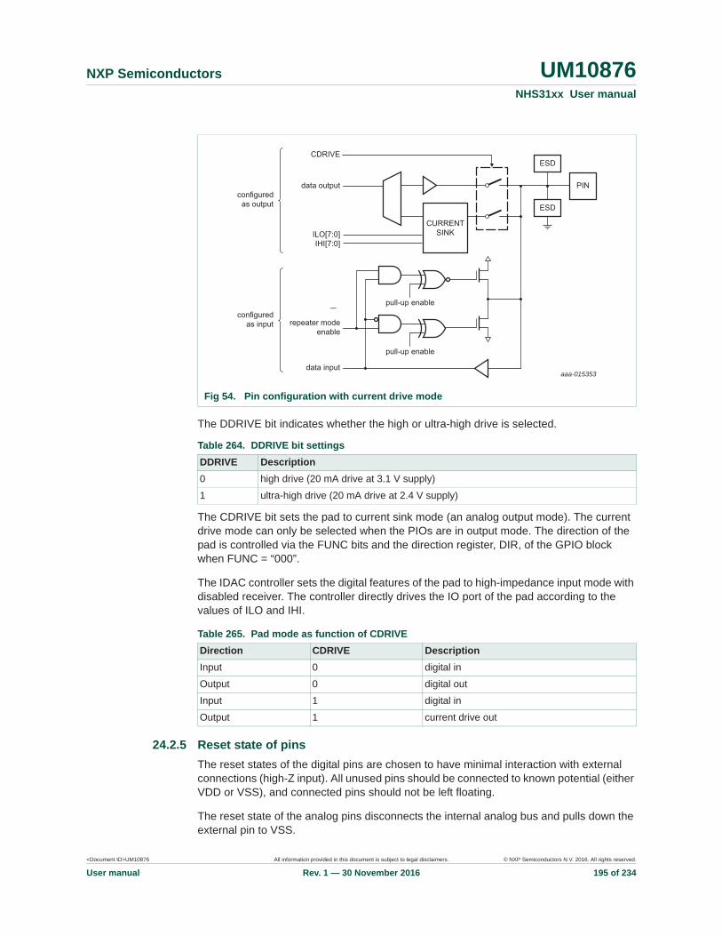
<Document ID>UM10876 All information provided in this document is subject to legal disclaimers. © NXP Semiconductors N.V. 2016. All rights reserved.
User manual Rev. 1 — 30 November 2016 195 of 234
NXP Semiconductors UM10876NHS31xx User manual
The DDRIVE bit indicates whether the high or ultra-high drive is selected.
The CDRIVE bit sets the pad to current sink mode (an analog output mode). The current drive mode can only be selected when the PIOs are in output mode. The direction of the pad is controlled via the FUNC bits and the direction register, DIR, of the GPIO block when FUNC = “000”.
The IDAC controller sets the digital features of the pad to high-impedance input mode with disabled receiver. The controller directly drives the IO port of the pad according to the values of ILO and IHI.
24.2.5 Reset state of pinsThe reset states of the digital pins are chosen to have minimal interaction with external connections (high-Z input). All unused pins should be connected to known potential (either VDD or VSS), and connected pins should not be left floating.
The reset state of the analog pins disconnects the internal analog bus and pulls down the external pin to VSS.
Fig 54. Pin configuration with current drive mode
Table 264. DDRIVE bit settingsDDRIVE Description0 high drive (20 mA drive at 3.1 V supply)
1 ultra-high drive (20 mA drive at 2.4 V supply)
Table 265. Pad mode as function of CDRIVEDirection CDRIVE DescriptionInput 0 digital in
Output 0 digital out
Input 1 digital in
Output 1 current drive out
aaa-015353
repeater modeenable
configuredas output
configuredas input
data input
data output
CDRIVE
IHI[7:0]ILO[7:0]
CURRENTSINK
pull-up enable
pull-up enable
ESD
ESD
PIN
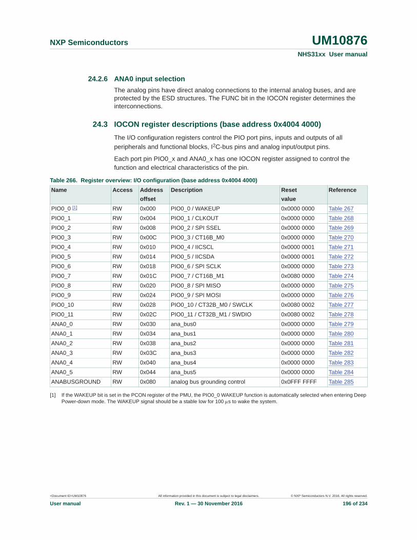
<Document ID>UM10876 All information provided in this document is subject to legal disclaimers. © NXP Semiconductors N.V. 2016. All rights reserved.
User manual Rev. 1 — 30 November 2016 196 of 234
NXP Semiconductors UM10876NHS31xx User manual
24.2.6 ANA0 input selectionThe analog pins have direct analog connections to the internal analog buses, and are protected by the ESD structures. The FUNC bit in the IOCON register determines the interconnections.
24.3 IOCON register descriptions (base address 0x4004 4000)The I/O configuration registers control the PIO port pins, inputs and outputs of all peripherals and functional blocks, I2C-bus pins and analog input/output pins.
Each port pin PIO0_x and ANA0_x has one IOCON register assigned to control the function and electrical characteristics of the pin.
[1] If the WAKEUP bit is set in the PCON register of the PMU, the PIO0_0 WAKEUP function is automatically selected when entering Deep Power-down mode. The WAKEUP signal should be a stable low for 100 s to wake the system.
Table 266. Register overview: I/O configuration (base address 0x4004 4000)Name Access Address
offsetDescription Reset
valueReference
PIO0_0 [1] RW 0x000 PIO0_0 / WAKEUP 0x0000 0000 Table 267
PIO0_1 RW 0x004 PIO0_1 / CLKOUT 0x0000 0000 Table 268
PIO0_2 RW 0x008 PIO0_2 / SPI SSEL 0x0000 0000 Table 269
PIO0_3 RW 0x00C PIO0_3 / CT16B_M0 0x0000 0000 Table 270
PIO0_4 RW 0x010 PIO0_4 / IICSCL 0x0000 0001 Table 271
PIO0_5 RW 0x014 PIO0_5 / IICSDA 0x0000 0001 Table 272
PIO0_6 RW 0x018 PIO0_6 / SPI SCLK 0x0000 0000 Table 273
PIO0_7 RW 0x01C PIO0_7 / CT16B_M1 0x0080 0000 Table 274
PIO0_8 RW 0x020 PIO0_8 / SPI MISO 0x0000 0000 Table 275
PIO0_9 RW 0x024 PIO0_9 / SPI MOSI 0x0000 0000 Table 276
PIO0_10 RW 0x028 PIO0_10 / CT32B_M0 / SWCLK 0x0080 0002 Table 277
PIO0_11 RW 0x02C PIO0_11 / CT32B_M1 / SWDIO 0x0080 0002 Table 278
ANA0_0 RW 0x030 ana_bus0 0x0000 0000 Table 279
ANA0_1 RW 0x034 ana_bus1 0x0000 0000 Table 280
ANA0_2 RW 0x038 ana_bus2 0x0000 0000 Table 281
ANA0_3 RW 0x03C ana_bus3 0x0000 0000 Table 282
ANA0_4 RW 0x040 ana_bus4 0x0000 0000 Table 283
ANA0_5 RW 0x044 ana_bus5 0x0000 0000 Table 284
ANABUSGROUND RW 0x080 analog bus grounding control 0x0FFF FFFF Table 285
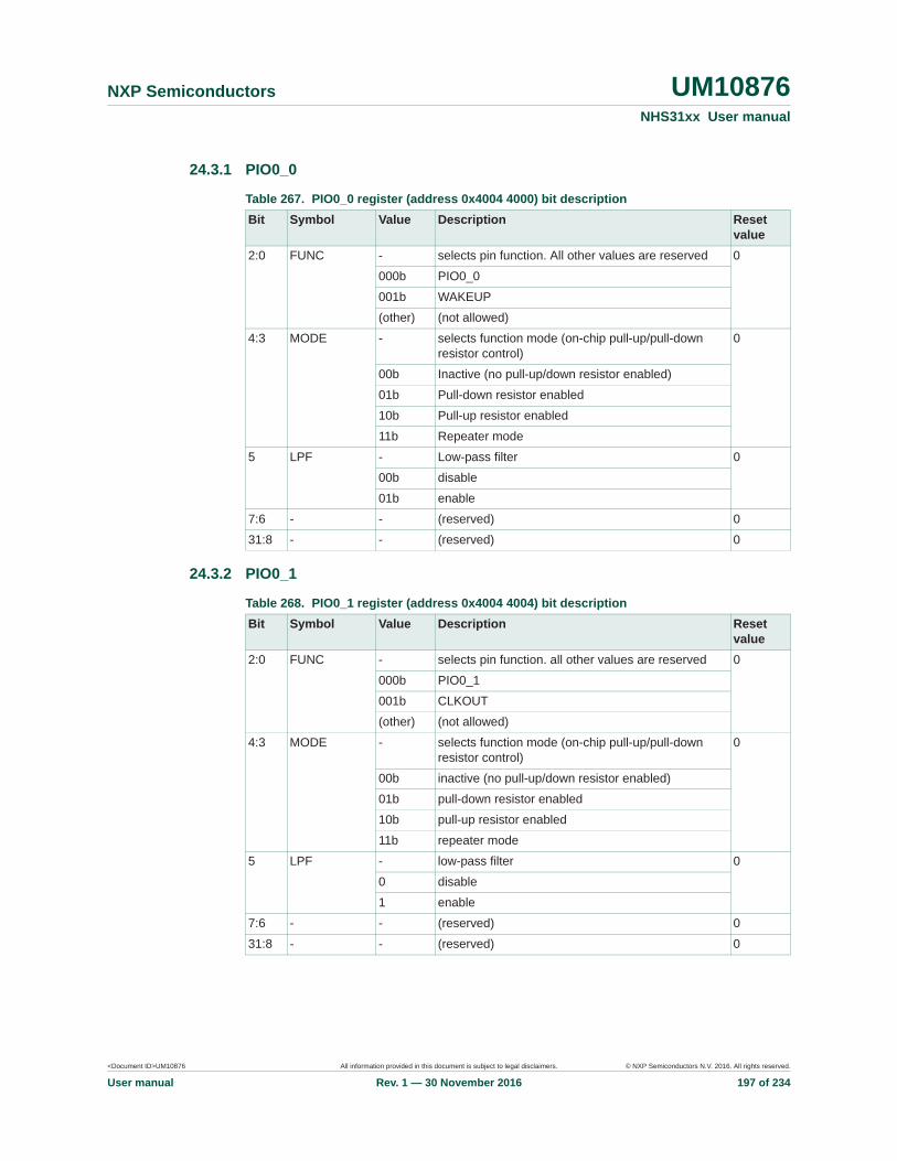
<Document ID>UM10876 All information provided in this document is subject to legal disclaimers. © NXP Semiconductors N.V. 2016. All rights reserved.
User manual Rev. 1 — 30 November 2016 197 of 234
NXP Semiconductors UM10876NHS31xx User manual
24.3.1 PIO0_0
24.3.2 PIO0_1
Table 267. PIO0_0 register (address 0x4004 4000) bit descriptionBit Symbol Value Description Reset
value2:0 FUNC - selects pin function. All other values are reserved 0
000b PIO0_0
001b WAKEUP
(other) (not allowed)
4:3 MODE - selects function mode (on-chip pull-up/pull-down resistor control)
0
00b Inactive (no pull-up/down resistor enabled)
01b Pull-down resistor enabled
10b Pull-up resistor enabled
11b Repeater mode
5 LPF - Low-pass filter 0
00b disable
01b enable
7:6 - - (reserved) 0
31:8 - - (reserved) 0
Table 268. PIO0_1 register (address 0x4004 4004) bit descriptionBit Symbol Value Description Reset
value2:0 FUNC - selects pin function. all other values are reserved 0
000b PIO0_1
001b CLKOUT
(other) (not allowed)
4:3 MODE - selects function mode (on-chip pull-up/pull-down resistor control)
0
00b inactive (no pull-up/down resistor enabled)
01b pull-down resistor enabled
10b pull-up resistor enabled
11b repeater mode
5 LPF - low-pass filter 0
0 disable
1 enable
7:6 - - (reserved) 0
31:8 - - (reserved) 0

<Document ID>UM10876 All information provided in this document is subject to legal disclaimers. © NXP Semiconductors N.V. 2016. All rights reserved.
User manual Rev. 1 — 30 November 2016 198 of 234
NXP Semiconductors UM10876NHS31xx User manual
24.3.3 PIO0_2
24.3.4 PIO0_3PIO0_3 is a high-drive, dual-mode (voltage and current sink) source/sink pad.
Table 269. PIO0_2 register (address 0x4004 4008) bit descriptionBit Symbol Value Description Reset
value2:0 FUNC - selects pin function. all other values are reserved 0
000b PIO0_2
001b SPI/SSP SSEL
(other) (not allowed)
4:3 MODE - selects function mode (on-chip pull-up/pull-down resistor control)
0
00b inactive (no pull-up/down resistor enabled)
01b pull-down resistor enabled
10b pull-up resistor enabled
11b repeater mode
5 LPF - low-pass filter 0
0 disable
1 enable
7:6 - - (reserved) 0
31:8 - - (reserved) 0
Table 270. PIO0_3 register (address 0x4004 400C) bit descriptionBit Symbol Value Description Reset
value2:0 FUNC - selects pin function. all other values are reserved 0
000b PIO0_3
001b CT16B_M0
(other) (not allowed)
4:3 MODE - selects function mode (on-chip pull-up/pull-down resistor control)
0
00b inactive (no pull-up/down resistor enabled)
01b pull-down resistor enabled
10b pull-up resistor enabled
11b repeater mode
5 LPF - low-pass filter 0
0 disable
1 enable
6 CDRIVE-
- select pin output driver 0
0 fixed voltage driver
1 programmable current driver
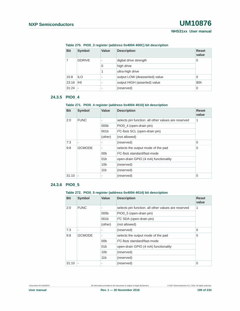
<Document ID>UM10876 All information provided in this document is subject to legal disclaimers. © NXP Semiconductors N.V. 2016. All rights reserved.
User manual Rev. 1 — 30 November 2016 199 of 234
NXP Semiconductors UM10876NHS31xx User manual
24.3.5 PIO0_4
24.3.6 PIO0_5
7 DDRIVE - digital drive strength 0
0 high drive
1 ultra-high drive
15:8 ILO - output LOW (deasserted) value 0
23:16 IHI - output HIGH (asserted) value 80h
31:24 - - (reserved) 0
Table 270. PIO0_3 register (address 0x4004 400C) bit descriptionBit Symbol Value Description Reset
value
Table 271. PIO0_4 register (address 0x4004 4010) bit descriptionBit Symbol Value Description Reset
value2:0 FUNC - selects pin function. all other values are reserved 1
000b PIO0_4 (open-drain pin)
001b I2C-bus SCL (open-drain pin)
(other) (not allowed)
7:3 - - (reserved) 0
9:8 I2CMODE - selects the output mode of the pad 0
00b I2C-bus standard/fast-mode
01b open-drain GPIO (4 mA) functionality
10b (reserved)
11b (reserved)
31:10 - - (reserved) 0
Table 272. PIO0_5 register (address 0x4004 4014) bit descriptionBit Symbol Value Description Reset
value2:0 FUNC - selects pin function. all other values are reserved 1
000b PIO0_5 (open-drain pin)
001b I2C SDA (open-drain pin)
(other) (not allowed)
7:3 - - (reserved) 0
9:8 I2CMODE - selects the output mode of the pad 0
00b I2C-bus standard/fast-mode
01b open-drain GPIO (4 mA) functionality
10b (reserved)
11b (reserved)
31:10 - - (reserved) 0
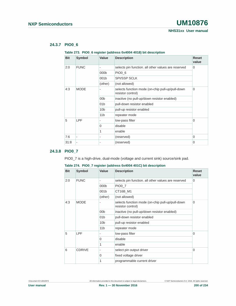
<Document ID>UM10876 All information provided in this document is subject to legal disclaimers. © NXP Semiconductors N.V. 2016. All rights reserved.
User manual Rev. 1 — 30 November 2016 200 of 234
NXP Semiconductors UM10876NHS31xx User manual
24.3.7 PIO0_6
24.3.8 PIO0_7
PIO0_7 is a high-drive, dual-mode (voltage and current sink) source/sink pad.
Table 273. PIO0_6 register (address 0x4004 4018) bit descriptionBit Symbol Value Description Reset
value2:0 FUNC - selects pin function. all other values are reserved 0
000b PIO0_6
001b SPI/SSP SCLK
(other) (not allowed)
4:3 MODE - selects function mode (on-chip pull-up/pull-down resistor control)
0
00b inactive (no pull-up/down resistor enabled)
01b pull-down resistor enabled
10b pull-up resistor enabled
11b repeater mode
5 LPF - low-pass filter 0
0 disable
1 enable
7:6 - - (reserved) 0
31:8 - - (reserved) 0
Table 274. PIO0_7 register (address 0x4004 401C) bit descriptionBit Symbol Value Description Reset
value2:0 FUNC - selects pin function. all other values are reserved 0
000b PIO0_7
001b CT16B_M1
(other) (not allowed)
4:3 MODE - selects function mode (on-chip pull-up/pull-down resistor control)
0
00b inactive (no pull-up/down resistor enabled)
01b pull-down resistor enabled
10b pull-up resistor enabled
11b repeater mode
5 LPF - low-pass filter 0
0 disable
1 enable
6 CDRIVE - select pin output driver 0
0 fixed voltage driver
1 programmable current driver

<Document ID>UM10876 All information provided in this document is subject to legal disclaimers. © NXP Semiconductors N.V. 2016. All rights reserved.
User manual Rev. 1 — 30 November 2016 201 of 234
NXP Semiconductors UM10876NHS31xx User manual
24.3.9 PIO0_8
24.3.10 PIO0_9
7 DDRIVE - digital drive strength -
0 high drive
1 ultra-high drive
15:8 ILO - output LOW (deasserted) value 0
23:16 IHI - output HIGH (asserted) value 80h
31:24 - - (reserved) 0
Table 274. PIO0_7 register (address 0x4004 401C) bit description _continued
Bit Symbol Value Description Reset value
Table 275. PIO0_8 register (address 0x4004 4020) bit descriptionBit Symbol Value Description Reset
value2:0 FUNC - selects pin function. all other values are reserved 0
000b PIO0_8
001b SPI/SSP MISO
(other) (not allowed)
4:3 MODE - selects function mode (on-chip pull-up/pull-down resistor control)
0
00b inactive (no pull-up/down resistor enabled)
01b pull-down resistor enabled
10b pull-up resistor enabled
11b repeater mode
5 LPF - low-pass filter 0
0 disable
1 enable
7:6 - - (reserved) 0
31:8 - - (reserved) 0
Table 276. PIO0_9 register (address 0x4004 4024) bit descriptionBit Symbol Value Description Reset
value2:0 FUNC - selects pin function. all other values are reserved 0
000b PIO0_9
001b SPI/SSP MOSI
(other) (not allowed)
4:3 MODE - selects function mode (on-chip pull-up/pull-down resistor control)
0
00b inactive (no pull-up/down resistor enabled)
01b pull-down resistor enabled
10b pull-up resistor enabled
11b repeater mode
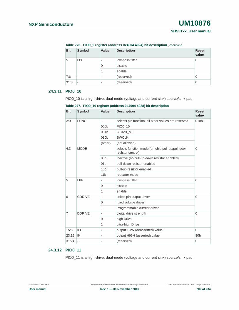
<Document ID>UM10876 All information provided in this document is subject to legal disclaimers. © NXP Semiconductors N.V. 2016. All rights reserved.
User manual Rev. 1 — 30 November 2016 202 of 234
NXP Semiconductors UM10876NHS31xx User manual
24.3.11 PIO0_10
PIO0_10 is a high-drive, dual-mode (voltage and current sink) source/sink pad.
24.3.12 PIO0_11
PIO0_11 is a high-drive, dual-mode (voltage and current sink) source/sink pad.
5 LPF - low-pass filter 0
0 disable
1 enable
7:6 - - (reserved) 0
31:8 - - (reserved) 0
Table 276. PIO0_9 register (address 0x4004 4024) bit description _continued
Bit Symbol Value Description Reset value
Table 277. PIO0_10 register (address 0x4004 4028) bit descriptionBit Symbol Value Description Reset
value2:0 FUNC - selects pin function. all other values are reserved 010b
000b PIO0_10
001b CT32B_M0
010b SWCLK
(other) (not allowed)
4:3 MODE - selects function mode (on-chip pull-up/pull-down resistor control)
0
00b inactive (no pull-up/down resistor enabled)
01b pull-down resistor enabled
10b pull-up resistor enabled
11b repeater mode
5 LPF - low-pass filter 0
0 disable
1 enable
6 CDRIVE - select pin output driver 0
0 fixed voltage driver
1 Programmable current driver
7 DDRIVE - digital drive strength 0
0 high Drive
1 ultra-high Drive
15:8 ILO - output LOW (deasserted) value 0
23:16 IHI - output HIGH (asserted) value 80h
31:24 - - (reserved) 0

<Document ID>UM10876 All information provided in this document is subject to legal disclaimers. © NXP Semiconductors N.V. 2016. All rights reserved.
User manual Rev. 1 — 30 November 2016 203 of 234
NXP Semiconductors UM10876NHS31xx User manual
24.3.13 ANA0_0
Table 278. PIO0_11 register (address 0x4004 402C) bit descriptionBit Symbol Value Description Reset
value2:0 FUNC - selects pin function. All other values are reserved 010b
000b PIO0_11
001b CT32B_M1
010b SWDIO
(other) (not allowed)
4:3 MODE - selects function mode (on-chip pull-up/pull-down resistor control)
0
00b inactive (no pull-up/down resistor enabled)
01b pull-down resistor enabled
10b pull-up resistor enabled
11b repeater mode
5 LPF - low-Pass Filter 0
0 disable
1 enable
6 CDRIVE - select pin output driver 0
0 fixed voltage driver
1 programmable current driver
7 DDRIVE - digital drive strength 0
0 high drive pad
1 ultra-high drive pad
15:8 ILO - output LOW (deasserted) value 0
23:16 IHI - output HIGH (asserted) value 80h
31:24 - - (reserved) 0
Table 279. ANA0_0 register (address 0x4004 4030) bit descriptionBit Symbol Value Description Reset
value2:0 FUNC - selects pin function. All other values are reserved 0
000b connect to VSS
001b connect to ana_extbus0
(other) (not allowed)
7:3 - - (reserved) 0
31:8 - - (reserved) 0
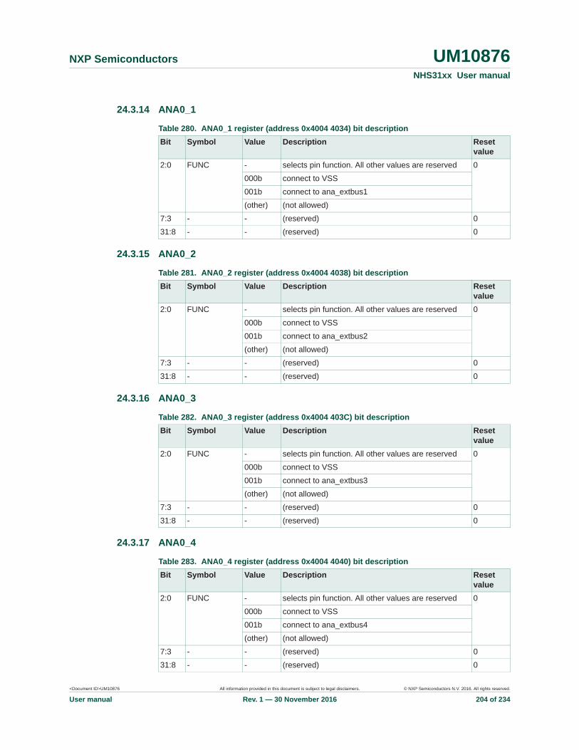
<Document ID>UM10876 All information provided in this document is subject to legal disclaimers. © NXP Semiconductors N.V. 2016. All rights reserved.
User manual Rev. 1 — 30 November 2016 204 of 234
NXP Semiconductors UM10876NHS31xx User manual
24.3.14 ANA0_1
24.3.15 ANA0_2
24.3.16 ANA0_3
24.3.17 ANA0_4
Table 280. ANA0_1 register (address 0x4004 4034) bit descriptionBit Symbol Value Description Reset
value2:0 FUNC - selects pin function. All other values are reserved 0
000b connect to VSS
001b connect to ana_extbus1
(other) (not allowed)
7:3 - - (reserved) 0
31:8 - - (reserved) 0
Table 281. ANA0_2 register (address 0x4004 4038) bit descriptionBit Symbol Value Description Reset
value2:0 FUNC - selects pin function. All other values are reserved 0
000b connect to VSS
001b connect to ana_extbus2
(other) (not allowed)
7:3 - - (reserved) 0
31:8 - - (reserved) 0
Table 282. ANA0_3 register (address 0x4004 403C) bit descriptionBit Symbol Value Description Reset
value2:0 FUNC - selects pin function. All other values are reserved 0
000b connect to VSS
001b connect to ana_extbus3
(other) (not allowed)
7:3 - - (reserved) 0
31:8 - - (reserved) 0
Table 283. ANA0_4 register (address 0x4004 4040) bit descriptionBit Symbol Value Description Reset
value2:0 FUNC - selects pin function. All other values are reserved 0
000b connect to VSS
001b connect to ana_extbus4
(other) (not allowed)
7:3 - - (reserved) 0
31:8 - - (reserved) 0
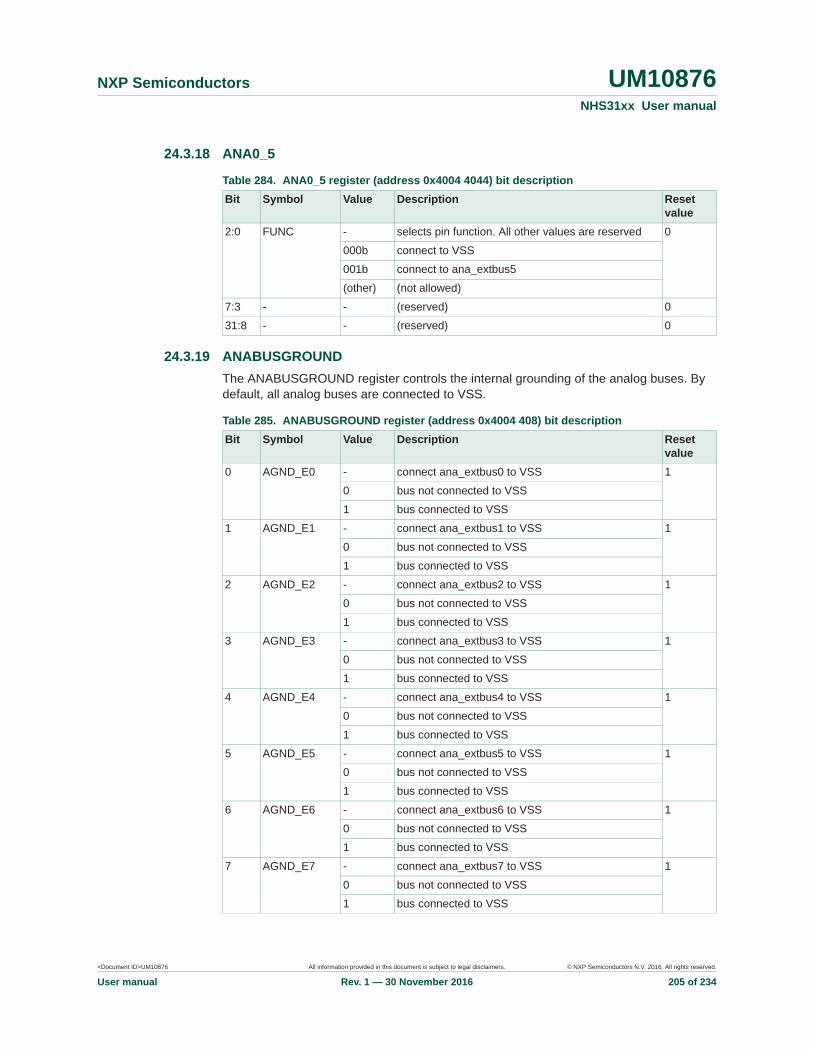
<Document ID>UM10876 All information provided in this document is subject to legal disclaimers. © NXP Semiconductors N.V. 2016. All rights reserved.
User manual Rev. 1 — 30 November 2016 205 of 234
NXP Semiconductors UM10876NHS31xx User manual
24.3.18 ANA0_5
24.3.19 ANABUSGROUNDThe ANABUSGROUND register controls the internal grounding of the analog buses. By default, all analog buses are connected to VSS.
Table 284. ANA0_5 register (address 0x4004 4044) bit descriptionBit Symbol Value Description Reset
value2:0 FUNC - selects pin function. All other values are reserved 0
000b connect to VSS
001b connect to ana_extbus5
(other) (not allowed)
7:3 - - (reserved) 0
31:8 - - (reserved) 0
Table 285. ANABUSGROUND register (address 0x4004 408) bit descriptionBit Symbol Value Description Reset
value0 AGND_E0 - connect ana_extbus0 to VSS 1
0 bus not connected to VSS
1 bus connected to VSS
1 AGND_E1 - connect ana_extbus1 to VSS 1
0 bus not connected to VSS
1 bus connected to VSS
2 AGND_E2 - connect ana_extbus2 to VSS 1
0 bus not connected to VSS
1 bus connected to VSS
3 AGND_E3 - connect ana_extbus3 to VSS 1
0 bus not connected to VSS
1 bus connected to VSS
4 AGND_E4 - connect ana_extbus4 to VSS 1
0 bus not connected to VSS
1 bus connected to VSS
5 AGND_E5 - connect ana_extbus5 to VSS 1
0 bus not connected to VSS
1 bus connected to VSS
6 AGND_E6 - connect ana_extbus6 to VSS 1
0 bus not connected to VSS
1 bus connected to VSS
7 AGND_E7 - connect ana_extbus7 to VSS 1
0 bus not connected to VSS
1 bus connected to VSS
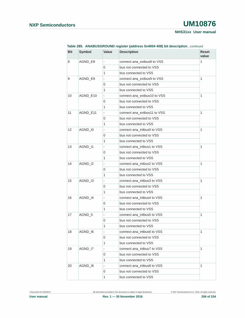
<Document ID>UM10876 All information provided in this document is subject to legal disclaimers. © NXP Semiconductors N.V. 2016. All rights reserved.
User manual Rev. 1 — 30 November 2016 206 of 234
NXP Semiconductors UM10876NHS31xx User manual
8 AGND_E8 - connect ana_extbus8 to VSS 1
0 bus not connected to VSS
1 bus connected to VSS
9 AGND_E9 - connect ana_extbus9 to VSS 1
0 bus not connected to VSS
1 bus connected to VSS
10 AGND_E10 - connect ana_extbus10 to VSS 1
0 bus not connected to VSS
1 bus connected to VSS
11 AGND_E11 - connect ana_extbus11 to VSS 1
0 bus not connected to VSS
1 bus connected to VSS
12 AGND_I0 - connect ana_intbus0 to VSS 1
0 bus not connected to VSS
1 bus connected to VSS
13 AGND_I1 - connect ana_intbus1 to VSS 1
0 bus not connected to VSS
1 bus connected to VSS
14 AGND_I2 - connect ana_intbus2 to VSS 1
0 bus not connected to VSS
1 bus connected to VSS
15 AGND_I3 - connect ana_intbus3 to VSS 1
0 bus not connected to VSS
1 bus connected to VSS
16 AGND_I4 - connect ana_intbus4 to VSS 1
0 bus not connected to VSS
1 bus connected to VSS
17 AGND_5 - connect ana_intbus5 to VSS 1
0 bus not connected to VSS
1 bus connected to VSS
18 AGND_I6 - connect ana_intbus6 to VSS 1
0 bus not connected to VSS
1 bus connected to VSS
19 AGND_I7 - connect ana_intbus7 to VSS 1
0 bus not connected to VSS
1 bus connected to VSS
20 AGND_I8 - connect ana_intbus8 to VSS 1
0 bus not connected to VSS
1 bus connected to VSS
Table 285. ANABUSGROUND register (address 0x4004 408) bit description _continued
Bit Symbol Value Description Reset value

<Document ID>UM10876 All information provided in this document is subject to legal disclaimers. © NXP Semiconductors N.V. 2016. All rights reserved.
User manual Rev. 1 — 30 November 2016 207 of 234
NXP Semiconductors UM10876NHS31xx User manual
21 AGND_I9 - connect ana_intbus9 to VSS 1
0 bus not connected to VSS
1 bus connected to VSS
22 AGND_I10 - connect ana_intbus10 to VSS 1
0 bus not connected to VSS
1 bus connected to VSS
23 AGND_I11 - connect ana_intbus11 to VSS 1
0 bus not connected to VSS
1 bus connected to VSS
24 AGND_I12 - connect ana_intbus12 to VSS 1
0 bus not connected to VSS
1 bus connected to VSS
25 AGND_I13 - connect ana_intbus13 to VSS 1
0 bus not connected to VSS
1 bus connected to VSS
26 AGND_I14 - connect ana_intbus14 to VSS 1
0 bus not connected to VSS
1 bus connected to VSS
27 AGND_I15 - connect ana_intbus15 to VSS 1
0 bus not connected to VSS
1 bus connected to VSS
Table 285. ANABUSGROUND register (address 0x4004 408) bit description _continued
Bit Symbol Value Description Reset value

<Document ID>UM10876 All information provided in this document is subject to legal disclaimers. © NXP Semiconductors N.V. 2016. All rights reserved.
User manual Rev. 1 — 30 November 2016 208 of 234
NXP Semiconductors UM10876NHS31xx User manual
25. Nested Vectored Interrupt Controller
25.1 About this chapterThis chapter describes the Nested Vectored Interrupt Controller (NVIC).
The NVIC is identical on members of the NHS31xx family.
25.2 Features
• Nested Vectored Interrupt Controller that is a part of the ARM Cortex-M0+• Tightly coupled interrupt controller provides low interrupt latency• Controls system exceptions and peripheral interrupts• The NVIC supports 32 vectored interrupts• Four programmable interrupt priority levels with hardware priority level masking• Software interrupt generation
25.3 General descriptionThe NVIC is a part of the ARM Cortex-M0+. The processor automatically stacks its state on exception entry and unstacks this state on exception exit, with no instruction overhead. This action provides low latency exception handling.
25.3.1 Interrupt sourcesTable 286 lists the interrupt sources for each peripheral function. Each peripheral device may have one or more interrupt lines to the NVIC. Each line may represent more than one interrupt source. Interrupts with the same priority level are serviced in the order of their interrupt number.
See Section 25.4 for a detailed NVIC register description.
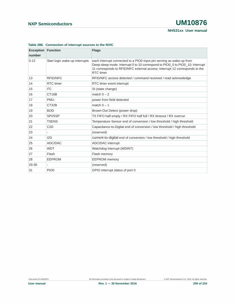
<Document ID>UM10876 All information provided in this document is subject to legal disclaimers. © NXP Semiconductors N.V. 2016. All rights reserved.
User manual Rev. 1 — 30 November 2016 209 of 234
NXP Semiconductors UM10876NHS31xx User manual
Table 286. Connection of interrupt sources to the NVICExceptionnumber
Function Flags
0-12 Start logic wake-up interrupts each interrupt connected to a PIO0 input pin serving as wake-up from Deep-sleep mode. Interrupt 0 to 10 correspond to PIO0_0 to PIO0_10; Interrupt 11 corresponds to RFID/NFC external access; Interrupt 12 corresponds to the RTC timer
13 RFID/NFC RFID/NFC access detected / command received / read acknowledge
14 RTC timer RTC timer event interrupt
15 I2C SI (state change)
16 CT16B match 0 – 2
17 PMU power from field detected
18 CT32B match 0 – 1
19 BOD Brown-Out Detect (power drop)
20 SPI/SSP TX FIFO half empty / RX FIFO half full / RX timeout / RX overrun
21 TSENS Temperature Sensor end of conversion / low threshold / high threshold
22 C2D Capacitance-to-Digital end of conversion / low threshold / high threshold
23 - (reserved)
24 I2D current-to-digital end of conversion / low threshold / high threshold
25 ADC/DAC ADC/DAC interrupt
26 WDT Watchdog interrupt (WDINT)
27 Flash Flash memory
28 EEPROM EEPROM memory
29-30 - (reserved)
31 PIO0 GPIO interrupt status of port 0

<Document ID>UM10876 All information provided in this document is subject to legal disclaimers. © NXP Semiconductors N.V. 2016. All rights reserved.
User manual Rev. 1 — 30 November 2016 210 of 234
NXP Semiconductors UM10876NHS31xx User manual
25.4 Register descriptionsThe NVIC registers are on the ARM private Peripheral Bus (APB).
Table 287. Register overview: NVIC (base address 0xE000 E000)Name Access Address
offsetDescription Reset
valueReference
ISER0 RW 0x100 Interrupt Set Enable Register 0. This register allows enabling interrupts and reading back the interrupt enables for specific peripheral functions
0 Table 288
- - 0x104 (reserved) - -
ICER0 RW 0x180 Interrupt Clear Enable Register 0. This register allows disabling interrupts and reading back the interrupt enables for specific peripheral functions
0 Table 289
- - 0x184 (reserved) - -
ISPR0 RW 0x200 Interrupt Set Pending Register 0. This register allows changing the interrupt state to pending and reading back the interrupt pending state for specific peripheral functions
0 Table 290
- - 0x204 (reserved) - -
ICPR0 RW 0x280 Interrupt Clear Pending Register 0. This register allows changing the interrupt state to not pending and reading back the interrupt pending state for specific peripheral functions
0 Table 291
- - 0x284 (reserved) - -
IABR0 RO 0x300 Interrupt Active Bit Register 0. This register allows reading the current interrupt active state for specific peripheral functions
0 Table 292
- - 0x304 (reserved) - -
IPR0 RW 0x400 Interrupt Priority Registers 0. This register allows assigning a priority to each interrupt. This register contains the 2-bit priority fields for interrupts 0 to 3
0 Table 293
IPR1 RW 0x404 Interrupt Priority Registers 1 This register allows assigning a priority to each interrupt. This register contains the 2-bit priority fields for interrupts 4 to 7
0 Table 294
IPR2 RW 0x408 Interrupt Priority Registers 2. This register allows assigning a priority to each interrupt. This register contains the 2-bit priority fields for interrupts 8 to 11
0 Table 295
IPR3 RW 0x40C Interrupt Priority Registers 3. This register allows assigning a priority to each interrupt. This register contains the 2-bit priority fields for interrupts 12 to 15
0 Table 296
- - 0x410 (reserved) - -
- - 0x414 (reserved) - -
IPR6 RW 0x418 Interrupt Priority Registers 6. This register allows assigning a priority to each interrupt. This register contains the 2-bit priority fields for interrupts 24 to 27
0 Table 297
IPR7 RW 0x41C Interrupt Priority Registers 7. This register allows assigning a priority to each interrupt. This register contains the 2-bit priority fields for interrupts 28 to 31
0 Table 298

<Document ID>UM10876 All information provided in this document is subject to legal disclaimers. © NXP Semiconductors N.V. 2016. All rights reserved.
User manual Rev. 1 — 30 November 2016 211 of 234
NXP Semiconductors UM10876NHS31xx User manual
25.4.1 Interrupt Set Enable Register 0 register (ISER0)The ISER0 register enables peripheral interrupts or contains the enabled state of those interrupts. Interrupts are disabled through the ICER0 register (See Section 25.4.2).
The bit description is as follows for all bits in this register:
Write — Writing logic 0 has no effect, writing logic 1 disables the interrupt.Read — Logic 0 indicates that the interrupt is disabled, logic 1 indicates that the interrupt is enabled.
Table 288. ISER0 register (address 0xE000 E100) bit descriptionBit Symbol Description Reset value0 ICE_SPI0 interrupt disable 0
1 ICE_SPI1 interrupt disable 0
2 - (reserved) -
3 ICE_UART0 interrupt disable 0
4 ICE_UART1 interrupt disable 0
5 ICE_UART2 interrupt disable 0
6 - (reserved) -
7 - (reserved) -
8 ICE_I2C interrupt disable 0
9 ICE_SCT interrupt disable 0
10 ICE_MRT interrupt disable 0
11 ICE_CMP interrupt disable 0
12 ICE_WDT interrupt disable 0
13 ICE_BOD interrupt disable 0
14 ICE_FLASH interrupt disable 0
15 ICE_WKT interrupt disable 0
16-23 - (reserved) -
24 ICE_PININT0 interrupt disable 0
25 ICE_PININT1 interrupt disable 0
26 ICE_PININT2 interrupt disable 0
27 ICE_PININT3 interrupt disable 0
28 ICE_PININT4 interrupt disable 0
29 ICE_PININT5 interrupt disable 0
30 ICE_PININT6 interrupt disable 0
31 ICE_PININT7 interrupt disable 0

<Document ID>UM10876 All information provided in this document is subject to legal disclaimers. © NXP Semiconductors N.V. 2016. All rights reserved.
User manual Rev. 1 — 30 November 2016 212 of 234
NXP Semiconductors UM10876NHS31xx User manual
25.4.2 Interrupt clear enable register 0 (ICER0)The ICER0 register allows disabling the peripheral interrupts, or for reading the enabled state of those interrupts. Enable interrupts through the ISER0 registers (See Section 25.4.1).
The bit description is as follows for all bits in this register:
Write — Writing logic 0 has no effect, writing logic 1 disables the interrupt.Read — Logic 0 indicates that the interrupt is disabled, logic 1 indicates that the interrupt is enabled.
Table 289. ICER0 register (address 0xE000 E180) bit descriptionBit Symbol Description Reset value0 ICE_SPI0 interrupt disable 0
1 ICE_SPI1 interrupt disable 0
2 - (reserved) -
3 ICE_UART0 interrupt disable 0
4 ICE_UART1 interrupt disable 0
5 ICE_UART2 interrupt disable 0
6 - (reserved) -
7 - (reserved) -
8 ICE_I2C interrupt disable 0
9 ICE_SCT interrupt disable 0
10 ICE_MRT interrupt disable 0
11 ICE_CMP interrupt disable 0
12 ICE_WDT interrupt disable 0
13 ICE_BOD interrupt disable 0
14 ICE_FLASH interrupt disable 0
15 ICE_WKT interrupt disable 0
16-23 - (reserved) -
24 ICE_PININT0 interrupt disable 0
25 ICE_PININT1 interrupt disable 0
26 ICE_PININT2 interrupt disable 0
27 ICE_PININT3 interrupt disable 0
28 ICE_PININT4 interrupt disable 0
29 ICE_PININT5 interrupt disable 0
30 ICE_PININT6 interrupt disable 0
31 ICE_PININT7 interrupt disable 0
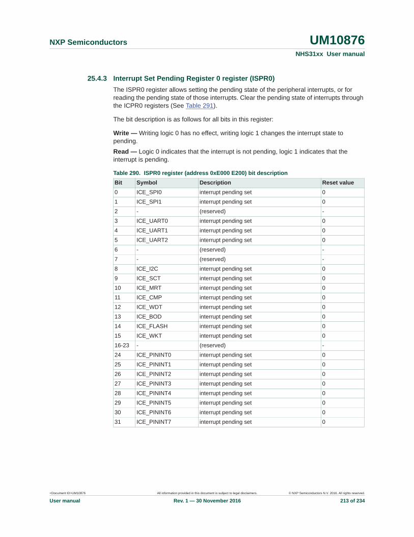
<Document ID>UM10876 All information provided in this document is subject to legal disclaimers. © NXP Semiconductors N.V. 2016. All rights reserved.
User manual Rev. 1 — 30 November 2016 213 of 234
NXP Semiconductors UM10876NHS31xx User manual
25.4.3 Interrupt Set Pending Register 0 register (ISPR0)The ISPR0 register allows setting the pending state of the peripheral interrupts, or for reading the pending state of those interrupts. Clear the pending state of interrupts through the ICPR0 registers (See Table 291).
The bit description is as follows for all bits in this register:
Write — Writing logic 0 has no effect, writing logic 1 changes the interrupt state to pending.Read — Logic 0 indicates that the interrupt is not pending, logic 1 indicates that the interrupt is pending.
Table 290. ISPR0 register (address 0xE000 E200) bit descriptionBit Symbol Description Reset value0 ICE_SPI0 interrupt pending set 0
1 ICE_SPI1 interrupt pending set 0
2 - (reserved) -
3 ICE_UART0 interrupt pending set 0
4 ICE_UART1 interrupt pending set 0
5 ICE_UART2 interrupt pending set 0
6 - (reserved) -
7 - (reserved) -
8 ICE_I2C interrupt pending set 0
9 ICE_SCT interrupt pending set 0
10 ICE_MRT interrupt pending set 0
11 ICE_CMP interrupt pending set 0
12 ICE_WDT interrupt pending set 0
13 ICE_BOD interrupt pending set 0
14 ICE_FLASH interrupt pending set 0
15 ICE_WKT interrupt pending set 0
16-23 - (reserved) -
24 ICE_PININT0 interrupt pending set 0
25 ICE_PININT1 interrupt pending set 0
26 ICE_PININT2 interrupt pending set 0
27 ICE_PININT3 interrupt pending set 0
28 ICE_PININT4 interrupt pending set 0
29 ICE_PININT5 interrupt pending set 0
30 ICE_PININT6 interrupt pending set 0
31 ICE_PININT7 interrupt pending set 0

<Document ID>UM10876 All information provided in this document is subject to legal disclaimers. © NXP Semiconductors N.V. 2016. All rights reserved.
User manual Rev. 1 — 30 November 2016 214 of 234
NXP Semiconductors UM10876NHS31xx User manual
25.4.4 Interrupt Clear Pending Register 0 register (ICPR0)The ICPR0 register allows clearing the pending state of the peripheral interrupts, or for reading the pending state of those interrupts. Set the pending state of interrupts through the ISPR0 register (See Table 290).
The bit description is as follows for all bits in this register:
Write — Writing logic 0 has no effect, writing logic 1 changes the interrupt state to not pending.Read — Logic 0 indicates that the interrupt is not pending, logic 1 indicates that the interrupt is pending.
Table 291. ICPR0 register (address 0xE000 E280) bit descriptionBit Symbol Description Reset value0 ICE_SPI0 interrupt pending clear 0
1 ICE_SPI1 interrupt pending clear 0
2 - (reserved) -
3 ICE_UART0 interrupt pending clear 0
4 ICE_UART1 interrupt pending clear 0
5 ICE_UART2 interrupt pending clear 0
6 - (reserved) -
7 - (reserved) -
8 ICE_I2C interrupt pending clear 0
9 ICE_SCT interrupt pending clear 0
10 ICE_MRT interrupt pending clear 0
11 ICE_CMP interrupt pending clear 0
12 ICE_WDT interrupt pending clear 0
13 ICE_BOD interrupt pending clear 0
14 ICE_FLASH interrupt pending clear 0
15 ICE_WKT interrupt pending clear 0
16-23 - (reserved) -
24 ICE_PININT0 interrupt pending clear 0
25 ICE_PININT1 interrupt pending clear 0
26 ICE_PININT2 interrupt pending clear 0
27 ICE_PININT3 interrupt pending clear 0
28 ICE_PININT4 interrupt pending clear 0
29 ICE_PININT5 interrupt pending clear 0
30 ICE_PININT6 interrupt pending clear 0
31 ICE_PININT7 interrupt pending clear 0
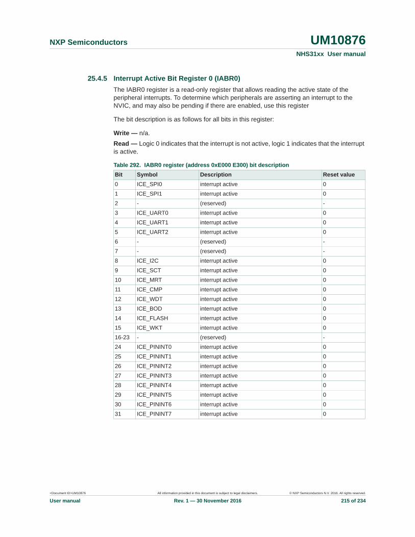
<Document ID>UM10876 All information provided in this document is subject to legal disclaimers. © NXP Semiconductors N.V. 2016. All rights reserved.
User manual Rev. 1 — 30 November 2016 215 of 234
NXP Semiconductors UM10876NHS31xx User manual
25.4.5 Interrupt Active Bit Register 0 (IABR0)The IABR0 register is a read-only register that allows reading the active state of the peripheral interrupts. To determine which peripherals are asserting an interrupt to the NVIC, and may also be pending if there are enabled, use this register
The bit description is as follows for all bits in this register:
Write — n/a.Read — Logic 0 indicates that the interrupt is not active, logic 1 indicates that the interrupt is active.
Table 292. IABR0 register (address 0xE000 E300) bit descriptionBit Symbol Description Reset value0 ICE_SPI0 interrupt active 0
1 ICE_SPI1 interrupt active 0
2 - (reserved) -
3 ICE_UART0 interrupt active 0
4 ICE_UART1 interrupt active 0
5 ICE_UART2 interrupt active 0
6 - (reserved) -
7 - (reserved) -
8 ICE_I2C interrupt active 0
9 ICE_SCT interrupt active 0
10 ICE_MRT interrupt active 0
11 ICE_CMP interrupt active 0
12 ICE_WDT interrupt active 0
13 ICE_BOD interrupt active 0
14 ICE_FLASH interrupt active 0
15 ICE_WKT interrupt active 0
16-23 - (reserved) -
24 ICE_PININT0 interrupt active 0
25 ICE_PININT1 interrupt active 0
26 ICE_PININT2 interrupt active 0
27 ICE_PININT3 interrupt active 0
28 ICE_PININT4 interrupt active 0
29 ICE_PININT5 interrupt active 0
30 ICE_PININT6 interrupt active 0
31 ICE_PININT7 interrupt active 0

<Document ID>UM10876 All information provided in this document is subject to legal disclaimers. © NXP Semiconductors N.V. 2016. All rights reserved.
User manual Rev. 1 — 30 November 2016 216 of 234
NXP Semiconductors UM10876NHS31xx User manual
25.4.6 Interrupt Priority Register 0 (IPR0)The IPR0 register controls the priority of four peripheral interrupts. Each interrupt can have one of 4 priorities, where 0 is the highest priority.
25.4.7 Interrupt Priority Register 1 (IPR1)The IPR1 register controls the priority of four peripheral interrupts. Each interrupt can have one of 4 priorities, where 0 is the highest priority.
25.4.8 Interrupt Priority Register 2 (IPR2)The IPR2 register controls the priority of four peripheral interrupts. Each interrupt can have one of 4 priorities, where 0 is the highest priority.
Table 293. IPR0 register (address 0xE000 E400) bit descriptionBit Symbol Description0:5 - these bits ignore writes, and read as logic 0
6:7 IP_SPI0 Interrupt Priority. 0 = highest priority. 3 = lowest priority
8:13 - these bits ignore writes, and read as logic 0
14:15 IP_SPI1 Interrupt Priority. 0 = highest priority. 3 = lowest priority
16:21 - these bits ignore writes, and read as logic 0
22:23 - (reserved)
24:29 - these bits ignore writes, and read as logic 0
30:31 IP_UART0 Interrupt Priority. 0 = highest priority. 3 = lowest priority
Table 294. IPR1 register (address 0xE000 E404) bit descriptionBit Symbol Description0:5 - these bits ignore writes, and read as logic 0
6:7 IP_UART1 Interrupt Priority. 0 = highest priority. 3 = lowest priority
8:13 - these bits ignore writes, and read as logic 0
14:15 IP_UART2 Interrupt Priority. 0 = highest priority. 3 = lowest priority
16:21 - these bits ignore writes, and read as logic 0
22:23 - (reserved)
24:29 - these bits ignore writes, and read as logic 0
30:31 - (reserved)
Table 295. IPR2 register (address 0xE000 E408) bit descriptionBit Symbol Description0:5 - these bits ignore writes, and read as logic 0
6:7 IP_I2C Interrupt Priority. 0 = highest priority. 3 = lowest priority
8:13 - these bits ignore writes, and read as logic 0
14:15 IP_SCT Interrupt Priority. 0 = highest priority. 3 = lowest priority
16:21 - these bits ignore writes, and read as logic 0
22:23 IP_MRT Interrupt Priority. 0 = highest priority. 3 = lowest priority
24:29 - these bits ignore writes, and read as logic 0
30:31 IP_CMP Interrupt Priority. 0 = highest priority. 3 = lowest priority
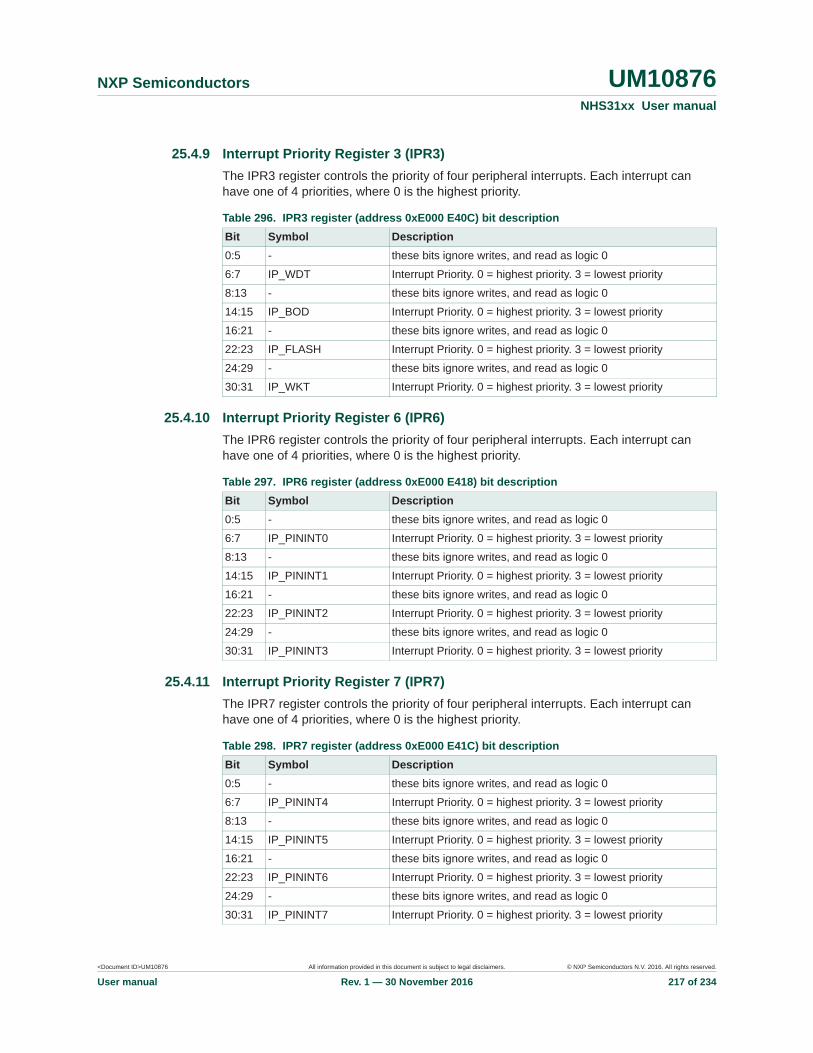
<Document ID>UM10876 All information provided in this document is subject to legal disclaimers. © NXP Semiconductors N.V. 2016. All rights reserved.
User manual Rev. 1 — 30 November 2016 217 of 234
NXP Semiconductors UM10876NHS31xx User manual
25.4.9 Interrupt Priority Register 3 (IPR3)The IPR3 register controls the priority of four peripheral interrupts. Each interrupt can have one of 4 priorities, where 0 is the highest priority.
25.4.10 Interrupt Priority Register 6 (IPR6)The IPR6 register controls the priority of four peripheral interrupts. Each interrupt can have one of 4 priorities, where 0 is the highest priority.
25.4.11 Interrupt Priority Register 7 (IPR7)The IPR7 register controls the priority of four peripheral interrupts. Each interrupt can have one of 4 priorities, where 0 is the highest priority.
Table 296. IPR3 register (address 0xE000 E40C) bit descriptionBit Symbol Description0:5 - these bits ignore writes, and read as logic 0
6:7 IP_WDT Interrupt Priority. 0 = highest priority. 3 = lowest priority
8:13 - these bits ignore writes, and read as logic 0
14:15 IP_BOD Interrupt Priority. 0 = highest priority. 3 = lowest priority
16:21 - these bits ignore writes, and read as logic 0
22:23 IP_FLASH Interrupt Priority. 0 = highest priority. 3 = lowest priority
24:29 - these bits ignore writes, and read as logic 0
30:31 IP_WKT Interrupt Priority. 0 = highest priority. 3 = lowest priority
Table 297. IPR6 register (address 0xE000 E418) bit descriptionBit Symbol Description0:5 - these bits ignore writes, and read as logic 0
6:7 IP_PININT0 Interrupt Priority. 0 = highest priority. 3 = lowest priority
8:13 - these bits ignore writes, and read as logic 0
14:15 IP_PININT1 Interrupt Priority. 0 = highest priority. 3 = lowest priority
16:21 - these bits ignore writes, and read as logic 0
22:23 IP_PININT2 Interrupt Priority. 0 = highest priority. 3 = lowest priority
24:29 - these bits ignore writes, and read as logic 0
30:31 IP_PININT3 Interrupt Priority. 0 = highest priority. 3 = lowest priority
Table 298. IPR7 register (address 0xE000 E41C) bit descriptionBit Symbol Description0:5 - these bits ignore writes, and read as logic 0
6:7 IP_PININT4 Interrupt Priority. 0 = highest priority. 3 = lowest priority
8:13 - these bits ignore writes, and read as logic 0
14:15 IP_PININT5 Interrupt Priority. 0 = highest priority. 3 = lowest priority
16:21 - these bits ignore writes, and read as logic 0
22:23 IP_PININT6 Interrupt Priority. 0 = highest priority. 3 = lowest priority
24:29 - these bits ignore writes, and read as logic 0
30:31 IP_PININT7 Interrupt Priority. 0 = highest priority. 3 = lowest priority
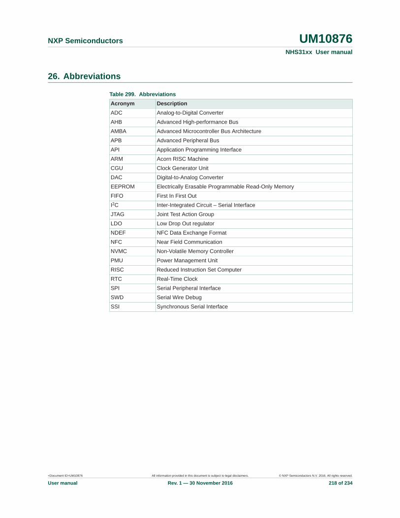
<Document ID>UM10876 All information provided in this document is subject to legal disclaimers. © NXP Semiconductors N.V. 2016. All rights reserved.
User manual Rev. 1 — 30 November 2016 218 of 234
NXP Semiconductors UM10876NHS31xx User manual
26. Abbreviations
Table 299. AbbreviationsAcronym DescriptionADC Analog-to-Digital Converter
AHB Advanced High-performance Bus
AMBA Advanced Microcontroller Bus Architecture
APB Advanced Peripheral Bus
API Application Programming Interface
ARM Acorn RISC Machine
CGU Clock Generator Unit
DAC Digital-to-Analog Converter
EEPROM Electrically Erasable Programmable Read-Only Memory
FIFO First In First Out
I2C Inter-Integrated Circuit – Serial Interface
JTAG Joint Test Action Group
LDO Low Drop Out regulator
NDEF NFC Data Exchange Format
NFC Near Field Communication
NVMC Non-Volatile Memory Controller
PMU Power Management Unit
RISC Reduced Instruction Set Computer
RTC Real-Time Clock
SPI Serial Peripheral Interface
SWD Serial Wire Debug
SSI Synchronous Serial Interface

<Document ID>UM10876 All information provided in this document is subject to legal disclaimers. © NXP Semiconductors N.V. 2016. All rights reserved.
User manual Rev. 1 — 30 November 2016 219 of 234
NXP Semiconductors UM10876NHS31xx User manual
27. References
[1] AN11340 — MIFARE Ultralight and MIFARE Ultralight EV1 features and hints[2] MF0ULx1 — MF0ULx1 MIFARE Ultralight EV1 - Contactless ticket IC[3] DUI0662B_cortex_m0p_r0p1_dgug — Cortex-M0+ Devices - Generic User Guide[4] DDI0484C_cortex_m0p_r0p1_trm — Cortex-M0+ Devices - Technical Reference
Manual[5] AN11657 — NHS3 Temperature sensor calibration
[6] ISO/IEEE 11073-10472 — Health informatics -- Point-of-care medical device communication -- Device specialization -- Medication monitor

<Document ID>UM10876 All information provided in this document is subject to legal disclaimers. © NXP Semiconductors N.V. 2016. All rights reserved.
User manual Rev. 1 — 30 November 2016 220 of 234
NXP Semiconductors UM10876NHS31xx User manual
28. Legal information
28.1 DefinitionsDraft — The document is a draft version only. The content is still under internal review and subject to formal approval, which may result in modifications or additions. NXP Semiconductors does not give any representations or warranties as to the accuracy or completeness of information included herein and shall have no liability for the consequences of use of such information.
28.2 DisclaimersLimited warranty and liability — Information in this document is believed to be accurate and reliable. However, NXP Semiconductors does not give any representations or warranties, expressed or implied, as to the accuracy or completeness of such information and shall have no liability for the consequences of use of such information. NXP Semiconductors takes no responsibility for the content in this document if provided by an information source outside of NXP Semiconductors.
In no event shall NXP Semiconductors be liable for any indirect, incidental, punitive, special or consequential damages (including - without limitation - lost profits, lost savings, business interruption, costs related to the removal or replacement of any products or rework charges) whether or not such damages are based on tort (including negligence), warranty, breach of contract or any other legal theory.
Notwithstanding any damages that customer might incur for any reason whatsoever, NXP Semiconductors’ aggregate and cumulative liability towards customer for the products described herein shall be limited in accordance with the Terms and conditions of commercial sale of NXP Semiconductors.
Right to make changes — NXP Semiconductors reserves the right to make changes to information published in this document, including without limitation specifications and product descriptions, at any time and without notice. This document supersedes and replaces all information supplied prior to the publication hereof.
Suitability for use — NXP Semiconductors products are not designed, authorized or warranted to be suitable for use in life support, life-critical or safety-critical systems or equipment, nor in applications where failure or malfunction of an NXP Semiconductors product can reasonably be expected to result in personal injury, death or severe property or environmental damage. NXP Semiconductors and its suppliers accept no liability for inclusion and/or use of NXP Semiconductors products in such equipment or applications and therefore such inclusion and/or use is at the customer’s own risk.
Applications — Applications that are described herein for any of these products are for illustrative purposes only. NXP Semiconductors makes no representation or warranty that such applications will be suitable for the specified use without further testing or modification.
Customers are responsible for the design and operation of their applications and products using NXP Semiconductors products, and NXP Semiconductors accepts no liability for any assistance with applications or customer product design. It is customer’s sole responsibility to determine whether the NXP Semiconductors product is suitable and fit for the customer’s applications and products planned, as well as for the planned application and use of customer’s third party customer(s). Customers should provide appropriate design and operating safeguards to minimize the risks associated with their applications and products.
NXP Semiconductors does not accept any liability related to any default, damage, costs or problem which is based on any weakness or default in the customer’s applications or products, or the application or use by customer’s third party customer(s). Customer is responsible for doing all necessary testing for the customer’s applications and products using NXP Semiconductors products in order to avoid a default of the applications and the products or of the application or use by customer’s third party customer(s). NXP does not accept any liability in this respect.
Limiting values — Stress above one or more limiting values (as defined in the Absolute Maximum Ratings System of IEC 60134) will cause permanent damage to the device. Limiting values are stress ratings only and (proper) operation of the device at these or any other conditions above those given in the Recommended operating conditions section (if present) or the Characteristics sections of this document is not warranted. Constant or repeated exposure to limiting values will permanently and irreversibly affect the quality and reliability of the device.
Terms and conditions of commercial sale — NXP Semiconductors products are sold subject to the general terms and conditions of commercial sale, as published at http://www.nxp.com/profile/terms, unless otherwise agreed in a valid written individual agreement. In case an individual agreement is concluded only the terms and conditions of the respective agreement shall apply. NXP Semiconductors hereby expressly objects to applying the customer’s general terms and conditions with regard to the purchase of NXP Semiconductors products by customer.
No offer to sell or license — Nothing in this document may be interpreted or construed as an offer to sell products that is open for acceptance or the grant, conveyance or implication of any license under any copyrights, patents or other industrial or intellectual property rights.
Export control — This document as well as the item(s) described herein may be subject to export control regulations. Export might require a prior authorization from competent authorities.
Evaluation products — This product is provided on an “as is” and “with all faults” basis for evaluation purposes only. NXP Semiconductors, its affiliates and their suppliers expressly disclaim all warranties, whether express, implied or statutory, including but not limited to the implied warranties of non-infringement, merchantability and fitness for a particular purpose. The entire risk as to the quality, or arising out of the use or performance, of this product remains with customer.
In no event shall NXP Semiconductors, its affiliates or their suppliers be liable to customer for any special, indirect, consequential, punitive or incidental damages (including without limitation damages for loss of business, business interruption, loss of use, loss of data or information, and the like) arising out the use of or inability to use the product, whether or not based on tort (including negligence), strict liability, breach of contract, breach of warranty or any other theory, even if advised of the possibility of such damages.
Notwithstanding any damages that customer might incur for any reason whatsoever (including without limitation, all damages referenced above and all direct or general damages), the entire liability of NXP Semiconductors, its affiliates and their suppliers and customer’s exclusive remedy for all of the foregoing shall be limited to actual damages incurred by customer based on reasonable reliance up to the greater of the amount actually paid by customer for the product or five dollars (US$5.00). The foregoing limitations, exclusions and disclaimers shall apply to the maximum extent permitted by applicable law, even if any remedy fails of its essential purpose.
Translations — A non-English (translated) version of a document is for reference only. The English version shall prevail in case of any discrepancy between the translated and English versions.
28.3 Licenses
Purchase of NXP ICs with NFC technology
Purchase of an NXP Semiconductors IC that complies with one of the Near Field Communication (NFC) standards ISO/IEC 18092 and ISO/IEC 21481 does not convey an implied license under any patent right infringed by implementation of any of those standards. Purchase of NXP Semiconductors IC does not include a license to any NXP patent (or other IP right) covering combinations of those products with other products, whether hardware or software.

<Document ID>UM10876 All information provided in this document is subject to legal disclaimers. © NXP Semiconductors N.V. 2016. All rights reserved.
User manual Rev. 1 — 30 November 2016 221 of 234
NXP Semiconductors UM10876NHS31xx User manual
28.4 TrademarksNotice: All referenced brands, product names, service names and trademarks are the property of their respective owners.
I2C-bus — logo is a trademark of NXP B.V.
MIFARE — is a trademark of NXP B.V.

<Document ID>UM10876 All information provided in this document is subject to legal disclaimers. © NXP Semiconductors N.V. 2016. All rights reserved.
User manual Rev. 1 — 30 November 2016 222 of 234
continued >>
NXP Semiconductors UM10876NHS31xx User manual
29. Tables
Table 1. Feature overview . . . . . . . . . . . . . . . . . . . . . . . .5Table 2. Ordering Information. . . . . . . . . . . . . . . . . . . . . .5Table 3. Pad allocation table of the HVQFN24 package 12Table 4. Pad description of the HVQFN24 package . . .13Table 5. Ball allocation table of the WLCSP25 package
15Table 6. Ball description of WLCSP25 package . . . . . .16Table 7. Register overview system configuration control
block - SYSCON (base address 0x4004 8000) 20Table 8. SYSMEMREMAP register (address 0x4004 8000)
bit description . . . . . . . . . . . . . . . . . . . . . . . . . .21Table 9. PRESETCTRL register (address 0x4004 8004)
bit description . . . . . . . . . . . . . . . . . . . . . . . . . .21Table 10. SYSCLKCTRL register (address 0x4004 8020)
bit description . . . . . . . . . . . . . . . . . . . . . . . . .22Table 11. Impact of different clock frequency settings . . .22Table 12. SYSCLKUEN register (address 0x4004 8024)
bit description . . . . . . . . . . . . . . . . . . . . . . . . . .23Table 13. SYSRSTSTAT register (address 0x4004 8030)
bit description . . . . . . . . . . . . . . . . . . . . . . . . . .23Table 14. SYSAHBCLKCTRL register (address 0x4004
8080) bit description . . . . . . . . . . . . . . . . . . . .24Table 15. SSPCLKDIV register (address 0x4004 8094)
bit description . . . . . . . . . . . . . . . . . . . . . . . . . .25Table 16. WDTCLKSEL register (address 0x4004 80D0)
bit description . . . . . . . . . . . . . . . . . . . . . . . . . .26Table 17. WDTCLKUEN register (address 0x4004 80D4)
bit description . . . . . . . . . . . . . . . . . . . . . . . . . .26Table 18. WDTCLKDIV register (address 0x4004 80D8)
bit description . . . . . . . . . . . . . . . . . . . . . . . . . .26Table 19. CLKOUTEN register (address 0x4004 80E8)
bit description . . . . . . . . . . . . . . . . . . . . . . . . . .27Table 20. SYSTCKCAL register (address 0x4004 8154)
bit description . . . . . . . . . . . . . . . . . . . . . . . . . .27Table 21. STARTAPRP0 register (address 0x4004 8200)
bit description . . . . . . . . . . . . . . . . . . . . . . . . . .27Table 22. STARTERP0 register (address 0x4004 8204)
bit description . . . . . . . . . . . . . . . . . . . . . . . . . .28Table 23. STARTRSRP0CLR register (address 0x4004
8208) bit description . . . . . . . . . . . . . . . . . . . .28Table 24. STARTSRP0 register (address 0x4004 820C)
bit description . . . . . . . . . . . . . . . . . . . . . . . . .29Table 25. PDAWAKECFG register (address 0x4004 8234)
bit description . . . . . . . . . . . . . . . . . . . . . . . . . .29Table 26. PDRUNCFG register (address 0x4004 8238)
bit description . . . . . . . . . . . . . . . . . . . . . . . . .30Table 27. DEVICE_ID register (address 0x4004 83F4)
bit description . . . . . . . . . . . . . . . . . . . . . . . . . .30
Table 28. Device IDs . . . . . . . . . . . . . . . . . . . . . . . . . . . . 30Table 29. IC power states . . . . . . . . . . . . . . . . . . . . . . . . 37Table 30. State transition events for DEEPSLEEP to
ACTIVE . . . . . . . . . . . . . . . . . . . . . . . . . . . . . . 38Table 31. State transition events for DEEP POWER-DOWN
to ACTIVE . . . . . . . . . . . . . . . . . . . . . . . . . . . . 38Table 32. Register overview: PMU (base address 0x4003
8000) . . . . . . . . . . . . . . . . . . . . . . . . . . . . . . . . 39Table 33. PCON register (address 0x4003 8000) bit
description . . . . . . . . . . . . . . . . . . . . . . . . . . . . 39Table 34. GPREG0 - GPREG3 registers (address 0x4003
8004 to 0x4003 8014) bit description. . . . . . . . 41Table 35. PSTAT register (address 0x4003 8018) bit
description . . . . . . . . . . . . . . . . . . . . . . . . . . . . 41Table 36. ACCSTAT register (address 0x4003 8020) bit
description . . . . . . . . . . . . . . . . . . . . . . . . . . . . 42Table 37. TMRCLKCTRL register (address 0x4003 802C)
bit description. . . . . . . . . . . . . . . . . . . . . . . . . . 42Table 38. IMSC register (address 0x4003 8030) bit
description . . . . . . . . . . . . . . . . . . . . . . . . . . . . 43Table 39. RIS register (address 0x4003 8034) bit
description . . . . . . . . . . . . . . . . . . . . . . . . . . . . 43Table 40. MIS register (address 0x4003 8038) bit
description . . . . . . . . . . . . . . . . . . . . . . . . . . . . 43Table 41. ICR register (address 0x4003 803C) bit
description . . . . . . . . . . . . . . . . . . . . . . . . . . . . 44Table 42. IAP command list . . . . . . . . . . . . . . . . . . . . . . . 46Table 43. IAP Read factory settings command . . . . . . . . 47Table 44. Supported registers for factory setting read. . . 47Table 45. IAP Prepare sectors for write operation
command . . . . . . . . . . . . . . . . . . . . . . . . . . . 48Table 46. IAP Copy data to flash command . . . . . . . . . . 48Table 47. IAP Erase sector command . . . . . . . . . . . . . . . 49Table 48. IAP Blank check sector command . . . . . . . . . . 49Table 49. IAP Read part identification command. . . . . . . 49Table 50. IAP Read boot code version number
command . . . . . . . . . . . . . . . . . . . . . . . . . . 50Table 51. IAP Compare command. . . . . . . . . . . . . . . . . . 50Table 52. IAP Read Unique Identification number
command . . . . . . . . . . . . . . . . . . . . . . . . . . 50Table 53. IAP Erase page command . . . . . . . . . . . . . . . . 51Table 54. IAP Status Codes. . . . . . . . . . . . . . . . . . . . . . . 51Table 55. Conversion time for different resolution of
TSENS . . . . . . . . . . . . . . . . . . . . . . . . . . . . 52Table 56. Register overview for temperature sensor (base
address 0x4006 0000) . . . . . . . . . . . . . . . . 53Table 57. CR register (address 0x4006 0000) bit
description . . . . . . . . . . . . . . . . . . . . . . . . . 53
<Document ID>UM10876 All information provided in this document is subject to legal disclaimers. © NXP Semiconductors N.V. 2016. All rights reserved.
User manual Rev. 1 — 30 November 2016 223 of 234
continued >>
NXP Semiconductors UM10876NHS31xx User manual
Table 58. DR register (address 0x4006 0004) bit description . . . . . . . . . . . . . . . . . . . . . . . . .53
Table 59. SR register (address 0x4006 0008) bit description . . . . . . . . . . . . . . . . . . . . . . . .53
Table 60. SP0 register (address 0x4006 000C) bit description. . . . . . . . . . . . . . . . . . . . . . . . . . . . .54
Table 61. SP1 register (address 0x4006 0010) bit description . . . . . . . . . . . . . . . . . . . . . . . . . . . .54
Table 62. SP2 register (address 0x4006 0014) bit description . . . . . . . . . . . . . . . . . . . . . . . . . . . .54
Table 63. SP3 register (address 0x4006 0018) bit description . . . . . . . . . . . . . . . . . . . . . . . . . . . .55
Table 64. TLO register (address 0x4006 001C) bit description . . . . . . . . . . . . . . . . . . . . . . . . . . . .55
Table 65. THI register (address 0x4006 0020) bit description . . . . . . . . . . . . . . . . . . . . . . . . .55
Table 66. IMSC register (address 0x4006 0024) bit description . . . . . . . . . . . . . . . . . . . . . . . . . . . .55
Table 67. RIS register (address 0x4006 0028) bit description . . . . . . . . . . . . . . . . . . . . . . . . . . . .56
Table 68. MIS register (address 0x4006 002C) bit description . . . . . . . . . . . . . . . . . . . . . . . . . . . .56
Table 69. ICR register (address 0x4006 0030) bit description . . . . . . . . . . . . . . . . . . . . . . . . . . . .56
Table 70. Connections to the Current-to-Digital analog input multiplexer . . . . . . . . . . . . . . . . . . . . . . .58
Table 71. Register overview: Current-to-Digital converter (base address 0x4006 8000) . . . . . . . . . . . . . .59
Table 72. CR register (address 0x4006 8000) bit description . . . . . . . . . . . . . . . . . . . . . . . . .59
Table 73. DR register (address 0x4006 8004) bit description . . . . . . . . . . . . . . . . . . . . . . . . .60
Table 74. SR register (address 0x4006 8008) bit description . . . . . . . . . . . . . . . . . . . . . . . . .60
Table 75. SP0 register (address 0x4006 800C) bit description . . . . . . . . . . . . . . . . . . . . . . . . . . . .60
Table 76. SP1 register (address 0x4006 8010) bit description . . . . . . . . . . . . . . . . . . . . . . . . . . . .61
Table 77. SP2 register (address 0x4006 8014) bit description . . . . . . . . . . . . . . . . . . . . . . . . . . . .61
Table 78. SP3 register (address 0x4006 8018) bit description . . . . . . . . . . . . . . . . . . . . . . . . . . . .61
Table 79. MUX register (address 0x4006 801C) bit description . . . . . . . . . . . . . . . . . . . . . . . . . . . .62
Table 80. TLO register (address 0x4006 4020) bit description . . . . . . . . . . . . . . . . . . . . . . . . . . . .62
Table 81. THI register (address 0x4006 4024) bit description . . . . . . . . . . . . . . . . . . . . . . . . .62
Table 82. IMSC register (address 0x4006 8028) bit description . . . . . . . . . . . . . . . . . . . . . . . . . . . .62
Table 83. RIS register (address 0x4006 802C) bit
description . . . . . . . . . . . . . . . . . . . . . . . . . . . . 63Table 84. MIS register (address 0x4006 8030) bit
description . . . . . . . . . . . . . . . . . . . . . . . . . . . . 63Table 85. ICR register (address 0x4006 4034) bit
description . . . . . . . . . . . . . . . . . . . . . . . . . . . . 63Table 86. Connections to the analog input multiplexers. . 66Table 87. Register overview: Capacitance-to-Digital
converter (base address 0x4006 4000) . . . . . . 67Table 88. CR register (address 0x4006 4000) bit
description . . . . . . . . . . . . . . . . . . . . . . . . . 67Table 89. DR register (address 0x4006 4004) bit
description . . . . . . . . . . . . . . . . . . . . . . . . . 68Table 90. SR register (address 0x4006 4008) bit
description . . . . . . . . . . . . . . . . . . . . . . . . . 68Table 91. SP0 register (address 0x4006 400C) bit
description . . . . . . . . . . . . . . . . . . . . . . . . . . . . 68Table 92. SP1 register (address 0x4006 4010) bit
description . . . . . . . . . . . . . . . . . . . . . . . . . . . . 68Table 93. SP2 register (address 0x4006 4014) bit
description . . . . . . . . . . . . . . . . . . . . . . . . . . . . 69Table 94. MUXA register (address 0x4006 4018) bit
description . . . . . . . . . . . . . . . . . . . . . . . . . . . . 69Table 95. MUXB register (address 0x4006 401C) bit
description . . . . . . . . . . . . . . . . . . . . . . . . . . . . 69Table 96. C2DTLO register (address 0x4006 4020) bit
description . . . . . . . . . . . . . . . . . . . . . . . . . . . . 69Table 97. THI register (address 0x4006 4024) bit
description . . . . . . . . . . . . . . . . . . . . . . . . . 70Table 98. IMSC register (address 0x4006 4028) bit
description . . . . . . . . . . . . . . . . . . . . . . . . . . . . 70Table 99. RIS register (address 0x4006 402C) bit
description . . . . . . . . . . . . . . . . . . . . . . . . . . . . 70Table 100. MIS register (address 0x4006 4030) bit
description . . . . . . . . . . . . . . . . . . . . . . . . . . . . 71Table 101. ICR register (address 0x4006 4034) bit
description . . . . . . . . . . . . . . . . . . . . . . . . . . . . 71Table 102. Connections to ADC input and output
multiplexers . . . . . . . . . . . . . . . . . . . . . . . . . . . 73Table 103. Register overview: Analog-to-Digital /
Digital-to-Analog converter (base address 0x4001 C000) . . . . . . . . . . . . . . . . . . . . . . . . . 74
Table 104. CR register (address 0x4001 C000) bit description . . . . . . . . . . . . . . . . . . . . . . . . . 74
Table 105. ADCDR register (address 0x4001 C004) bit description . . . . . . . . . . . . . . . . . . . . . . . . . . . . 74
Table 106. DACDR register (address 0x4001 C008) bit description . . . . . . . . . . . . . . . . . . . . . . . . . . . . 75
Table 107. SR register (address 0x4001 C00C) bit description . . . . . . . . . . . . . . . . . . . . . . . . . . . . 75
Table 108. ADCSP register (address 0x4001 C010) bit description . . . . . . . . . . . . . . . . . . . . . . . . . . . . 75
<Document ID>UM10876 All information provided in this document is subject to legal disclaimers. © NXP Semiconductors N.V. 2016. All rights reserved.
User manual Rev. 1 — 30 November 2016 224 of 234
continued >>
NXP Semiconductors UM10876NHS31xx User manual
Table 109. ADCMUX register (address 0x4001 C018) bit description . . . . . . . . . . . . . . . . . . . . . . . . . . . .76
Table 110. DACMUX register (address 0x4001 C01C) bit description . . . . . . . . . . . . . . . . . . . . . . . . . . . .76
Table 111. ADCTLO register (address 0x4001 C020) bit description . . . . . . . . . . . . . . . . . . . . . . . . . . . .76
Table 112. ADC0THI register (address 0x4001 C024) bit description . . . . . . . . . . . . . . . . . . . . . . . . . . . .76
Table 113. IMSC register (address 0x4001 C028) bit description . . . . . . . . . . . . . . . . . . . . . . . . . . . .77
Table 114. RIS register (address 0x4001 C02C) bit description . . . . . . . . . . . . . . . . . . . . . . . . . . . .77
Table 115. MIS register (address 0x4001 C030) bit description . . . . . . . . . . . . . . . . . . . . . . . . . . . .77
Table 116. ADC0ICR register (address 0x4001 C034) bit description . . . . . . . . . . . . . . . . . . . . . . . . . . . .78
Table 117. RFID/NFC communication block register and buffer memory space overview: APB side . . . .82
Table 118. RFID/NFC communication block special registers and buffer memory space overview: RFID side 82
Table 119. CFG register (address 0x4005 8000) bit description . . . . . . . . . . . . . . . . . . . . . . . . . . . .83
Table 120. SR register (APB address 0x4005 8004, RF address 0x84) bit description . . . . . . . . . . . . . .83
Table 121. CMDIN register (APB address 0x4005 800C, RF address 0x85) bit description . . . . . . . . . . . . . .84
Table 122. CMDOUT register (APB address 0x4005 8010, RF address 0x86) bit description . . . . . . . . . . .84
Table 123. TARGET register (address 0x4005 8010) bit description . . . . . . . . . . . . . . . . . . . . . . . . . . . .85
Table 124. LAST_ACCESS register (address 0x4005 8014) bit description . . . . . . . . . . . . . . . . . . . . . . . . . .85
Table 125. IMSC register (address 0x4005 8014) bit description . . . . . . . . . . . . . . . . . . . . . . . . . . . .85
Table 126. RIS register (address 0x4005 801C) bit description . . . . . . . . . . . . . . . . . . . . . . . . . . . .85
Table 127. RIS register (address 0x4005 801C) bit description . . . . . . . . . . . . . . . . . . . . . . . . . . . .86
Table 128. ICR register (address 0x4005 8024) bit description . . . . . . . . . . . . . . . . . . . . . . . . . . . .86
Table 129. Register overview: RTC timer (base address 0x4005 4000) . . . . . . . . . . . . . . . . . . . . . . . . . .88
Table 130. RTC Timer control register (address 0x4005 4000) bit description . . . . . . . . . . . . . . . . . . . . .89
Table 131. RTC Timer status register (address 0x4005 4004) bit description . . . . . . . . . . . . . . . . . . . . . . . . . .89
Table 132. RTC timer calibration register (address 0x4005 4008) bit description . . . . . . . . . . . . . . . . . . . . .90
Table 133. RTC timer sleep time register (address 0x4005 400C) bit description. . . . . . . . . . . . . . . . . . . . .90
Table 134. RTC timer current value register (address 0x4005
4010) bit description. . . . . . . . . . . . . . . . . . . . . 90Table 135. IMSC register (address 0x4005 4014) bit
description . . . . . . . . . . . . . . . . . . . . . . . . . . . . 90Table 136. RIS register (address 0x4005 4018) bit
description . . . . . . . . . . . . . . . . . . . . . . . . . . . . 90Table 137. MIS register (address 0x4005 401C) bit
description . . . . . . . . . . . . . . . . . . . . . . . . . . . . 91Table 138. ICR register (address 0x4005 4020) bit
description . . . . . . . . . . . . . . . . . . . . . . . . . . . . 91Table 139. ACCSTAT register (address 0x4005 4024) bit
description . . . . . . . . . . . . . . . . . . . . . . . . . . . . 92Table 140. TIME register (address 0x4005 4030) bit
description . . . . . . . . . . . . . . . . . . . . . . . . . . . . 92Table 141. Register overview: Watchdog timer block (base
address 0x4000 4000) . . . . . . . . . . . . . . . . . . . 94Table 142. WDMOD register (address 0x4000 4000) bit
description . . . . . . . . . . . . . . . . . . . . . . . . . . . . 95Table 143. Watchdog Operating mode selection . . . . . . . 95Table 144. WDTC register (address 0x4000 4004) bit
description . . . . . . . . . . . . . . . . . . . . . . . . . . . . 96Table 145. WDFEED register (address 0x4000 4008) bit
description . . . . . . . . . . . . . . . . . . . . . . . . . . . . 96Table 146. WDTV register (address 0x4000 400C) bit
description . . . . . . . . . . . . . . . . . . . . . . . . . . . . 96Table 147. Register overview: SYSTICK timer (base address
0xE000 E000) . . . . . . . . . . . . . . . . . . . . . . . . . 98Table 148. CSR register (address 0xE000 E010) bit
description . . . . . . . . . . . . . . . . . . . . . . . . . . . . 99Table 149. RVR register (address 0xE000 E014) bit
description . . . . . . . . . . . . . . . . . . . . . . . . . . . . 99Table 150. CVR register (address 0xE000 E018) bit
description . . . . . . . . . . . . . . . . . . . . . . . . . . . 100Table 151. CALIB register (address 0xE000 E01C) bit
description . . . . . . . . . . . . . . . . . . . . . . . . . . . 100Table 152. Counter/timer pin description . . . . . . . . . . . . 103Table 153. Register overview: 16-bit timer 0 CT16B0 (base
address 0x4000 C000). . . . . . . . . . . . . . . . . . 106Table 154. IR register (address 0x4000 C000) bit
description . . . . . . . . . . . . . . . . . . . . . . . . 107Table 155. TCR register (address 0x4000 C004) bit
description . . . . . . . . . . . . . . . . . . . . . . . . . . . 107Table 156. TC register (address 0x4000 C008) bit
description . . . . . . . . . . . . . . . . . . . . . . . . . . . 107Table 157. PR register (address 0x4000 C00C) bit
description . . . . . . . . . . . . . . . . . . . . . . . . . . . 107Table 158. PC register (address 0x4001 C010) bit
description . . . . . . . . . . . . . . . . . . . . . . . . . . . 108Table 159. MCR register (address 0x4000 C014) bit
description . . . . . . . . . . . . . . . . . . . . . . . . . . . 108Table 160. MR0/1/2/3 registers (addresses 0x4000 C018 to
24) bit description. . . . . . . . . . . . . . . . . . . . . . 109
<Document ID>UM10876 All information provided in this document is subject to legal disclaimers. © NXP Semiconductors N.V. 2016. All rights reserved.
User manual Rev. 1 — 30 November 2016 225 of 234
continued >>
NXP Semiconductors UM10876NHS31xx User manual
Table 161. EEMR register (address 0x4000 C03C) bit description . . . . . . . . . . . . . . . . . . . . . . . . . . . 110
Table 162. PWMC register (address 0x4000 C074) bit description . . . . . . . . . . . . . . . . . . . . . . . . . . . 111
Table 163. Counter/timer pin description . . . . . . . . . . . . . 113Table 164. Register overview: 32-bit counter/timer 0 CT32B
(base address 0x4000 4000) . . . . . . . . . . . . . 116Table 165. IR register (address 0x4000 4000) bit
description . . . . . . . . . . . . . . . . . . . . . . . . 117Table 166. TCR register (address 0x4000 4004) bit
description . . . . . . . . . . . . . . . . . . . . . . . . . . . 117Table 167. TC register (address 0x4000 4008) bit
description . . . . . . . . . . . . . . . . . . . . . . . . 117Table 168. PR register (address 0x4000 400C) bit
description . . . . . . . . . . . . . . . . . . . . . . . . . . . 117Table 169. PC register (address 0x4001 4010) bit
description . . . . . . . . . . . . . . . . . . . . . . . . 118Table 170. MCR register (address 0x4000 4014) bit
description . . . . . . . . . . . . . . . . . . . . . . . . . . . 118Table 171. MR0/1/2/3 registers (addresses 0x4000 4018 to
24) bit description . . . . . . . . . . . . . . . . . . . . . . 119Table 172. EMR register (address 0x4000 403C) bit
description . . . . . . . . . . . . . . . . . . . . . . . . . . .120Table 173. PWMC register (address 0x4000 4074) bit
description . . . . . . . . . . . . . . . . . . . . . . . . . . .121Table 174. Register overview: EEPROM memory controller
(base address 0x4003 4000) . . . . . . . . . . . . .123Table 175. RWSTATE register (address 0x4003 4008)
bit description . . . . . . . . . . . . . . . . . . . . . . . . .124Table 176. WSTATE register (address 0x4003 4010) bit
description . . . . . . . . . . . . . . . . . . . . . . . . . . .124Table 177. PAUTOPROG register (address 0x4003 400C)
bit description . . . . . . . . . . . . . . . . . . . . . . . . .124Table 178. CLKDIV register (address 0x4003 4014)
bit description . . . . . . . . . . . . . . . . . . . . . . . . .125Table 179. CLKDIV1 register (address 0x4003 4054)
bit description . . . . . . . . . . . . . . . . . . . . . . . . .125Table 180. CLKDIV2 register (address 0x4003 4058)
bit description . . . . . . . . . . . . . . . . . . . . . . . . .125Table 181. PWRDWN register (address 0x4003 4020)
bit description . . . . . . . . . . . . . . . . . . . . . . . . .125Table 182. MSSTART register (address 0x4003 4020)
bit description . . . . . . . . . . . . . . . . . . . . . . . . .126Table 183. MSSTOP register (address 0x4003 4024)
bit description . . . . . . . . . . . . . . . . . . . . . . . . .126Table 184. MSDATASIG register (address 0x4003 4028)
bit description . . . . . . . . . . . . . . . . . . . . . . . . .126Table 185. . . . MSPARSIG register (address 0x4003 402C)
bit description . . . . . . . . . . . . . . . . . . . . . . . . .126Table 186. STATUS register (address 0x4003 4034)
bit description . . . . . . . . . . . . . . . . . . . . . . . . .126
Table 187. ECCERRCNT register (address 0x4003 403C) bit description. . . . . . . . . . . . . . . . . . . . . . . . . 127
Table 188. INT_CLR_ENABLE register (address 0x4003 4FD8) bit description . . . . . . . . . . . . . . . . . . . 127
Table 189. INT_SET_ENABLE register (address 0x4003 4FDC) bit description . . . . . . . . . . . . . . . . . . . 127
Table 190. INT_CLR_STATUS register (address 0x4003 4FE8) bit description . . . . . . . . . . . . . . . . . . . 127
Table 191. INT_ENABLE register (address 0x4003 4FE0) bit description. . . . . . . . . . . . . . . . . . . . . . . . . 127
Table 192. INT_STATUS register (address 0x4003 4FE4) bit description . . . . . . . . . . . . . . . . . . . . . . . . 127
Table 193. MODULE_ID register (address 0x4003 4FFC) bit description. . . . . . . . . . . . . . . . . . . . . . . . . 128
Table 194. Feedback bits for MISR computation . . . . . . 133Table 195. Register overview: Flash memory controller
(base address 0x4004 C000). . . . . . . . . . . . . 134Table 196. FCTR register (address 0x4003 C000) bit
description . . . . . . . . . . . . . . . . . . . . . . . . . . . 134Table 197. FSTAT register (address 0x4003 C010) bit
description . . . . . . . . . . . . . . . . . . . . . . . . . . . 135Table 198. FBWST register (address 0x4003 C010) bit
description . . . . . . . . . . . . . . . . . . . . . . . . . . . 136Table 199. WST values for different Flash operating modes
(FCTR settings) and system clock speed . . . 136Table 200. FPTR register (address 0x4003 C008) bit
description . . . . . . . . . . . . . . . . . . . . . . . . . . . 136Table 201. FCRA register (address 0x4003 C01C) bit
description . . . . . . . . . . . . . . . . . . . . . . . . . . . 136Table 202. FMSSTART register (address 0x4003 C020)
bit description. . . . . . . . . . . . . . . . . . . . . . . . . 137Table 203. FMSSTOP register (address 0x4003 C024)
bit description. . . . . . . . . . . . . . . . . . . . . . . . . 137Table 204. FMS16 register (address 0x4003 C028) bit
description . . . . . . . . . . . . . . . . . . . . . . . . . . . 137Table 205. FMSW0 register (address 0x4003 C02C) bit
description . . . . . . . . . . . . . . . . . . . . . . . . . . . 137Table 206. ECCRSTERRCNT register (address 0x4003
C050) bit description . . . . . . . . . . . . . . . . . . . 137Table 207. ECCERRCNT register (address 0x4003 C054)
bit description. . . . . . . . . . . . . . . . . . . . . . . . . 137Table 208. INT_CLR_ENABLE register (address 0x4003
CFD8) bit description . . . . . . . . . . . . . . . . . . . 138Table 209. INT_SET_ENABLE register (address 0x4003
CFDC) bit description. . . . . . . . . . . . . . . . . . . 138Table 210. INT_CLR_STATUS register (address 0x4003
CFE8) bit description . . . . . . . . . . . . . . . . . . . 138Table 211. INT_SET_STATUS register (address 0x4003
CFEC) bit description. . . . . . . . . . . . . . . . . . . 138Table 212. . INT_ENABLE register (address 0x4003 CFE0)
bit description. . . . . . . . . . . . . . . . . . . . . . . . . 138
<Document ID>UM10876 All information provided in this document is subject to legal disclaimers. © NXP Semiconductors N.V. 2016. All rights reserved.
User manual Rev. 1 — 30 November 2016 226 of 234
continued >>
NXP Semiconductors UM10876NHS31xx User manual
Table 213. . . INT_STATUS register (address 0x4003 CFE4) bit description . . . . . . . . . . . . . . . . . . . . . . . . .138
Table 214. MODULE_ID register (address 0x4003 CFFC) bit description . . . . . . . . . . . . . . . . . . . . . . . . .139
Table 215. I2C-bus pin description. . . . . . . . . . . . . . . . . .141Table 216. Register overview of the I2C-bus controller (base
0x4000 000) . . . . . . . . . . . . . . . . . . . . . . . . . .142Table 217. CONSET register (address 0x4000 0000) bit
description . . . . . . . . . . . . . . . . . . . . . . . . . . .143Table 218. STAT register (address 0x4000 0004) bit
description . . . . . . . . . . . . . . . . . . . . . . . . . . .145Table 219. DAT register (address 0x4000 0008) bit
description . . . . . . . . . . . . . . . . . . . . . . . . . . .145Table 220. ADR0 register (address 0x4000 000C) bit
description . . . . . . . . . . . . . . . . . . . . . . . . . . .145Table 221. SCLH register (address 0x4000 0010) bit
description . . . . . . . . . . . . . . . . . . . . . . . . . . .145Table 222. SCLL register (address 0x4000 0014) bit
description . . . . . . . . . . . . . . . . . . . . . . . . . . .146Table 223. SCLL + SCLH values for selected I2C-bus clock
rates . . . . . . . . . . . . . . . . . . . . . . . . . . . . .146Table 224. CONCLR register (address 0x4000 0018) bit
description . . . . . . . . . . . . . . . . . . . . . . . . . . .146Table 225. MMCTRL register (address 0x4000 001C) bit
description . . . . . . . . . . . . . . . . . . . . . . . . . . .147Table 226. ADR1/2/3 registers (addresses 0x4000
0020,0024,0028) bit description . . . . . . . . . . .148Table 227. DATA_BUFFER register (address 0x4000 002C)
bit description . . . . . . . . . . . . . . . . . . . . . . . . .149Table 228. MASK0/1/2/3 register (addresses 0x4000
0030,0034,0038,003C) bit description . . . . . .149Table 229. CONSET used to configure Master mode . . .150Table 230. CONSET used to configure Slave mode . . . .151Table 231. Abbreviations used to describe an I2C-bus
operation . . . . . . . . . . . . . . . . . . . . . . . . . .157Table 232. CONSET used to initialize Master transmitter
mode. . . . . . . . . . . . . . . . . . . . . . . . . . . . . . . .157Table 233. Master transmitter mode . . . . . . . . . . . . . . . .158Table 234. Master receive mode . . . . . . . . . . . . . . . . . . .161Table 235. ADR usage in Slave receiver mode. . . . . . . .162Table 236. CONSET used to initialize Slave transmitter
mode. . . . . . . . . . . . . . . . . . . . . . . . . . . . . . . .163Table 237. Slave receiver mode . . . . . . . . . . . . . . . . . . .163Table 238. Slave transmitter mode . . . . . . . . . . . . . . . . .167Table 239. Miscellaneous States . . . . . . . . . . . . . . . . . . .169Table 240. SPI pin description. . . . . . . . . . . . . . . . . . . . .175Table 241. Register overview: Serial Peripheral Interface
(base address 0x4004 0000) . . . . . . . . . . . . .183Table 242. CR0 register (address 0x4004 0000) bit
description . . . . . . . . . . . . . . . . . . . . . . . . . . .184Table 243. CR1 register (address 0x4004 0004) bit
description . . . . . . . . . . . . . . . . . . . . . . . . . . . 185Table 244. DR register 0 (address 0x4004 0008) bit
description . . . . . . . . . . . . . . . . . . . . . . . . . . . 185Table 245. SR register (address 0x4004 000C) bit
description . . . . . . . . . . . . . . . . . . . . . . . . 186Table 246. CPSR register (address 0x4004 0010) bit
description . . . . . . . . . . . . . . . . . . . . . . . . . . . 186Table 247. IMSC register (address 0x4004 0014) bit
description . . . . . . . . . . . . . . . . . . . . . . . . . . . 186Table 248. RIS register (address 0x4004 0018) bit
description . . . . . . . . . . . . . . . . . . . . . . . . . . . 187Table 249. MIS register (address 0x4004 001C) bit
description . . . . . . . . . . . . . . . . . . . . . . . . . . . 187Table 250. ICR register (address 0x4004 0020) bit
description . . . . . . . . . . . . . . . . . . . . . . . . . . . 187Table 251. Register overview: General Purpose I/O (base
address 0x5000 0000) . . . . . . . . . . . . . . . . . . 188Table 252. GPIODATA register (address 0x5000 0000 to
0x5000 3FFC) bit description. . . . . . . . . . . . . 189Table 253. DIR register (address 0x5000 8000) bit
description . . . . . . . . . . . . . . . . . . . . . . . . . . . 189Table 254. IS register (address 0x5000 8004) bit
description . . . . . . . . . . . . . . . . . . . . . . . . 190Table 255. IBE register (address 0x5000 8008) bit
description . . . . . . . . . . . . . . . . . . . . . . . . . . . 190Table 256. IEV register (address 0x5000 800C) bit
description . . . . . . . . . . . . . . . . . . . . . . . . . . . 190Table 257. IMSC register (address 0x5000 8010) bit
description . . . . . . . . . . . . . . . . . . . . . . . . 190Table 258. RIS register (address 0x5000 8014) bit
description . . . . . . . . . . . . . . . . . . . . . . . . . . . 191Table 259. MIS register (address 0x5000 8018) bit
description . . . . . . . . . . . . . . . . . . . . . . . . . . . 191Table 260. IC register (address 0x5000 801C) bit
description . . . . . . . . . . . . . . . . . . . . . . . 191Table 261. Pad direction and MFIO settings. . . . . . . . . . 193Table 262. LPF bit and MFIO pad output selection. . . . . 194Table 263. Pad output behavior . . . . . . . . . . . . . . . . . . . 194Table 264. DDRIVE bit settings . . . . . . . . . . . . . . . . 195Table 265. Pad mode as function of CDRIVE. . . . . . . . . 195Table 266. Register overview: I/O configuration (base
address 0x4004 4000) . . . . . . . . . . . . . . . . . 196Table 267. PIO0_0 register (address 0x4004 4000) bit
description . . . . . . . . . . . . . . . . . . . . . . . . . . . 197Table 268. PIO0_1 register (address 0x4004 4004) bit
description . . . . . . . . . . . . . . . . . . . . . . . . . . . 197Table 269. PIO0_2 register (address 0x4004 4008) bit
description . . . . . . . . . . . . . . . . . . . . . . . . . . . 198Table 270. PIO0_3 register (address 0x4004 400C) bit
description . . . . . . . . . . . . . . . . . . . . . . . . . . . 198Table 271. PIO0_4 register (address 0x4004 4010) bit
<Document ID>UM10876 All information provided in this document is subject to legal disclaimers. © NXP Semiconductors N.V. 2016. All rights reserved.
User manual Rev. 1 — 30 November 2016 227 of 234
NXP Semiconductors UM10876NHS31xx User manual
description . . . . . . . . . . . . . . . . . . . . . . . . . . .199Table 272. PIO0_5 register (address 0x4004 4014) bit
description . . . . . . . . . . . . . . . . . . . . . . . . . . .199Table 273. PIO0_6 register (address 0x4004 4018) bit
description . . . . . . . . . . . . . . . . . . . . . . . . . . .200Table 274. PIO0_7 register (address 0x4004 401C) bit
description . . . . . . . . . . . . . . . . . . . . . . . . . . .200Table 275. PIO0_8 register (address 0x4004 4020) bit
description . . . . . . . . . . . . . . . . . . . . . . . . . . .201Table 276. PIO0_9 register (address 0x4004 4024) bit
description . . . . . . . . . . . . . . . . . . . . . . . . . . .201Table 277. PIO0_10 register (address 0x4004 4028) bit
description . . . . . . . . . . . . . . . . . . . . . . . . . . .202Table 278. PIO0_11 register (address 0x4004 402C) bit
description . . . . . . . . . . . . . . . . . . . . . . . . . . .203Table 279. ANA0_0 register (address 0x4004 4030) bit
description . . . . . . . . . . . . . . . . . . . . . . . . . . .203Table 280. ANA0_1 register (address 0x4004 4034) bit
description . . . . . . . . . . . . . . . . . . . . . . . . . . .204Table 281. ANA0_2 register (address 0x4004 4038) bit
description . . . . . . . . . . . . . . . . . . . . . . . . . . .204Table 282. ANA0_3 register (address 0x4004 403C) bit
description . . . . . . . . . . . . . . . . . . . . . . . . . . .204Table 283. ANA0_4 register (address 0x4004 4040) bit
description . . . . . . . . . . . . . . . . . . . . . . . . . . .204Table 284. ANA0_5 register (address 0x4004 4044) bit
description . . . . . . . . . . . . . . . . . . . . . . . . . . .205Table 285. ANABUSGROUND register (address 0x4004
408) bit description . . . . . . . . . . . . . . . . . . . .205Table 286. Connection of interrupt sources to the NVIC .209Table 287. Register overview: NVIC (base address 0xE000
E000) . . . . . . . . . . . . . . . . . . . . . . . . . . . . . . .210Table 288. ISER0 register (address 0xE000 E100) bit
description . . . . . . . . . . . . . . . . . . . . . . . . . . . 211Table 289. ICER0 register (address 0xE000 E180) bit
description . . . . . . . . . . . . . . . . . . . . . . . . . . .212Table 290. ISPR0 register (address 0xE000 E200) bit
description . . . . . . . . . . . . . . . . . . . . . . . . . . .213Table 291. ICPR0 register (address 0xE000 E280) bit
description . . . . . . . . . . . . . . . . . . . . . . . . . . .214Table 292. IABR0 register (address 0xE000 E300) bit
description . . . . . . . . . . . . . . . . . . . . . . . . . . .215Table 293. IPR0 register (address 0xE000 E400) bit
description . . . . . . . . . . . . . . . . . . . . . . . . . . .216Table 294. IPR1 register (address 0xE000 E404) bit
description . . . . . . . . . . . . . . . . . . . . . . . . . . .216Table 295. IPR2 register (address 0xE000 E408) bit
description . . . . . . . . . . . . . . . . . . . . . . . . . . .216Table 296. IPR3 register (address 0xE000 E40C) bit
description . . . . . . . . . . . . . . . . . . . . . . . . . . .217Table 297. IPR6 register (address 0xE000 E418) bit
description . . . . . . . . . . . . . . . . . . . . . . . . . . .217Table 298. IPR7 register (address 0xE000 E41C) bit
description . . . . . . . . . . . . . . . . . . . . . . . . . . .217Table 299. Abbreviations . . . . . . . . . . . . . . . . . . . . . . . .218

<Document ID>UM10876 All information provided in this document is subject to legal disclaimers. © NXP Semiconductors N.V. 2016. All rights reserved.
User manual Rev. 1 — 30 November 2016 228 of 234
NXP Semiconductors UM10876NHS31xx User manual
30. Figures
Fig 1. NHS3100 block diagram . . . . . . . . . . . . . . . . . . . .6Fig 2. NHS3152 block diagram . . . . . . . . . . . . . . . . . . . .6Fig 3. NHS3153 block diagram . . . . . . . . . . . . . . . . . . . .7Fig 4. NHS31xx family memory map . . . . . . . . . . . . . . . .9Fig 5. Pad configuration of HVQFN24 package. . . . . . .12Fig 6. Ball configuration of WLCSP25 package. . . . . . .15Fig 7. NHS31xx clock generator block diagram. . . . . . .19Fig 8. NHS31xx power architecture . . . . . . . . . . . . . . . .36Fig 9. Power rails and power supply pad types. . . . . . .37Fig 10. PMU state transition diagram. . . . . . . . . . . . . . . .37Fig 11. NHS31xx power-up sequence . . . . . . . . . . . . . . .38Fig 12. IAP command passing . . . . . . . . . . . . . . . . . . . . .45Fig 13. Current-to-Digital block diagram . . . . . . . . . . . . .57Fig 14. Capacitance-to-Digital block diagram . . . . . . . . .65Fig 15. Analog-to-Digital / Digital-to-Analog block
diagram . . . . . . . . . . . . . . . . . . . . . . . . . . . . .72Fig 16. NHS31xx analog bus structure . . . . . . . . . . . . . .79Fig 17. Block diagram of the RFID/NFC interface . . . . . .80Fig 18. Memory map as seen from RF interface . . . . . . .81Fig 19. System tick timer block diagram . . . . . . . . . . . . .98Fig 20. A timer cycle in which PR=2, MRx=6, and both
interrupt and reset on match are enabled . . . . .103Fig 21. A timer cycle in which PR=2, MRx=6, and both
interrupt and stop on match are enabled . . . . . .104Fig 22. 16-bit timer block diagram . . . . . . . . . . . . . . . . .105Fig 23. Sample PWM waveforms with a PWM cycle length
of 100 (selected by MR2) and MAT2:0 enabled as PWM outputs by the PWCM register. . . . . . . . . 111
Fig 24. A timer cycle in which PR=2, MRx=6, and both interrupt and reset on match are enabled . . . . . 114
Fig 25. A timer cycle in which PR=2, MRx=6, and both interrupt and stop on match are enabled . . . . . . 114
Fig 26. 32-bit counter/timer block diagram. . . . . . . . . . . 115Fig 27. Sample PWM waveforms with a PWM cycle length
of 100 (selected by MR2) and MAT2:0 enabled as PWM outputs by the PWCM register. . . . . . . . .121
Fig 28. Typical I2C-bus configuration . . . . . . . . . . . . . . .140Fig 29. Data format in the Master transmitter mode . . .150Fig 30. Data format of Master receiver mode . . . . . . . .151Fig 31. Master receiver switches to master transmitter after
sending Repeated-START . . . . . . . . . . . . . . . . .151Fig 32. Data format of Slave receiver mode . . . . . . . . .152Fig 33. Data format of Slave mode . . . . . . . . . . . . . . . .152Fig 34. I2C serial interface block diagram . . . . . . . . . . .153Fig 35. Arbitration procedure . . . . . . . . . . . . . . . . . . . . .155Fig 36. Serial clock synchronization. . . . . . . . . . . . . . . .155Fig 37. Format and states in the Master transmitter
mode . . . . . . . . . . . . . . . . . . . . . . . . . . . . . .160Fig 38. Format and states in Master receiver mode . . .162Fig 39. Format and states in Slave receiver mode . . . .166Fig 40. Format and states in Slave transmitter mode . .168Fig 41. Simultaneous Repeated-START conditions from
two masters . . . . . . . . . . . . . . . . . . . . . . . . . . . .170Fig 42. Forced access to a busy I2C-bus . . . . . . . . . . .171Fig 43. Recovering from a bus obstruction caused by a
LOW level on SDA. . . . . . . . . . . . . . . . . . . . . . .171
Fig 44. Texas Instruments synchronous Serial Frame Format: Single frame transfer (top), back-to-back two frames transfer (bottom) . . . . . . . . . . . . . . . 177
Fig 45. SPI bus timing . . . . . . . . . . . . . . . . . . . . . . . . . . 178Fig 46. SPI frame format with CPOL = logic 0 and CPHA =
logic 0. (a) Single and b) Continuous Transfer . 178Fig 47. SPI frame format with CPOL = logic 0 and CPHA =
logic 1 . . . . . . . . . . . . . . . . . . . . . . . . . . . . . . . . 179Fig 48. SPI frame format with CPOL = logic 1 and CPHA =
logic 0 (a) Single and b) Continuous Transfer) . 180Fig 49. SPI frame format with CPOL = logic 1 and CPHA =
logic 1 . . . . . . . . . . . . . . . . . . . . . . . . . . . . . . . . 181Fig 50. Microwire frame format (single transfer) . . . . . . 182Fig 51. Microwire frame format (continuous transfers) . 182Fig 52. Masked write operation to the GPIODATA
register . . . . . . . . . . . . . . . . . . . . . . . . . . . . 192Fig 53. Masked GPIO read operation . . . . . . . . . . . . . . 192Fig 54. Pin configuration with current drive mode . . . . . 195

<Document ID>UM10876 All information provided in this document is subject to legal disclaimers. © NXP Semiconductors N.V. 2016. All rights reserved.
User manual Rev. 1 — 30 November 2016 229 of 234
continued >>
NXP Semiconductors UM10876NHS31xx User manual
31. Contents
1 Introductory information. . . . . . . . . . . . . . . . . . 31.1 Introduction. . . . . . . . . . . . . . . . . . . . . . . . . . . . 31.2 Attributes . . . . . . . . . . . . . . . . . . . . . . . . . . . . . 31.3 Device-dependent features . . . . . . . . . . . . . . . 51.4 Ordering information. . . . . . . . . . . . . . . . . . . . . 51.5 Block diagrams . . . . . . . . . . . . . . . . . . . . . . . . . 6
NHS3100 Temperature logger . . . . . . . . . . . . . .6NHS3152 for therapy adherence using resistive sensing . . . . . . . . . . . . . . . . . . . . . . . . . . . . . . . .6NHS3153 for therapy adherence using capacitive sensing . . . . . . . . . . . . . . . . . . . . . . . . . . . . . . . .7
1.6 ARM Cortex-M0+ core configuration . . . . . . . . 81.7 Memory map. . . . . . . . . . . . . . . . . . . . . . . . . . . 81.7.1 Memories . . . . . . . . . . . . . . . . . . . . . . . . . . . . . 91.7.1.1 SRAM (0x1000 0000 to 0x1000 1FFF). . . . . . . 91.7.1.2 Flash (0x0000 0000 to 0x0000 7FFF) . . . . . . . 91.7.1.3 EEPROM (0x3000 0000 to 0x3000 0FFF) . . . 102 Product feature overview . . . . . . . . . . . . . . . . 112.1 About this chapter. . . . . . . . . . . . . . . . . . . . . . 112.2 General description . . . . . . . . . . . . . . . . . . . . 112.2.1 NHS3100 for cold chain monitoring and therapy
adherence. . . . . . . . . . . . . . . . . . . . . . . . . . . . 112.2.2 NHS3152 for therapy adherence using resistive
sensing . . . . . . . . . . . . . . . . . . . . . . . . . . . . . . 112.2.3 NHS3153 for therapy adherence using capacitive
sensing . . . . . . . . . . . . . . . . . . . . . . . . . . . . . . 113 Pinning . . . . . . . . . . . . . . . . . . . . . . . . . . . . . . . 123.1 About this chapter. . . . . . . . . . . . . . . . . . . . . . 123.2 Pinning . . . . . . . . . . . . . . . . . . . . . . . . . . . . . . 124 System configuration (SYSCON) . . . . . . . . . . 184.1 General description . . . . . . . . . . . . . . . . . . . . 184.2 Clock generation. . . . . . . . . . . . . . . . . . . . . . . 184.3 System FRO clock specifications . . . . . . . . . . 194.3.1 SFRO trimming. . . . . . . . . . . . . . . . . . . . . . . . 194.4 Timer FRO clock specifications . . . . . . . . . . . 194.5 Register description overview. . . . . . . . . . . . . 194.5.1 System memory remap register
(SYSMEMREMAP). . . . . . . . . . . . . . . . . . . . . 214.5.2 Peripheral reset control register
(PRESETCTRL) . . . . . . . . . . . . . . . . . . . . 214.5.3 System clock control register (SYSCLKCTRL) 214.5.4 System clock update enable register
(SYSCLKUEN) . . . . . . . . . . . . . . . . . . . . . . . . 234.5.5 System reset status register (SYSRSTSTAT). 234.5.6 AHB clock control register . . . . . . . . . . . . . . . 244.5.7 SPI/SSP clock divider control register
(SSPCLKDIV) . . . . . . . . . . . . . . . . . . . . . . . . . 25
4.5.8 Watchdog timer clock source selection register (WDTCLKSEL). . . . . . . . . . . . . . . . . . . . . . . . 25
4.5.9 Watchdog timer clock update enable register (WDTCLKUEN) . . . . . . . . . . . . . . . . . . . . . . . 26
4.5.10 Watchdog timer clock divider register (WDTCLKDIV) . . . . . . . . . . . . . . . . . . . . . . . . 26
4.5.11 clock output enable register (CLKOUTEN) . . 264.5.12 System tick counter calibration register
(SYSTCKCAL) . . . . . . . . . . . . . . . . . . . . . . . . 274.5.13 Start logic edge control register 0
(STARTAPRP0) . . . . . . . . . . . . . . . . . . . 274.5.14 Start logic signal enable register 0
(STARTERP0) . . . . . . . . . . . . . . . . . . . . 274.5.15 Start logic reset register 0
(STARTRSRP0CLR) . . . . . . . . . . . . . . . 284.5.16 Start logic status register 0 (STARTSRP0) . . 284.5.17 Wake-up configuration register
(PDAWAKECFG) . . . . . . . . . . . . . . . . . . . . 294.5.18 Power-down configuration register
(PDRUNCFG) . . . . . . . . . . . . . . . . . . . . . . . 294.5.19 Device ID register (DEVICE_ID) . . . . . . . . . . 305 Power management unit (PMU) . . . . . . . . . . . 315.1 About this chapter . . . . . . . . . . . . . . . . . . . . . 315.2 General description . . . . . . . . . . . . . . . . . . . . 315.3 Functional description . . . . . . . . . . . . . . . . . . 315.3.1 Active mode . . . . . . . . . . . . . . . . . . . . . . . . . . 315.3.1.1 Power configuration in Active mode. . . . . . . . 315.3.2 Sleep mode . . . . . . . . . . . . . . . . . . . . . . . . . . 325.3.3 Deep-sleep mode. . . . . . . . . . . . . . . . . . . . . . 325.3.4 Deep power-down mode . . . . . . . . . . . . . . . . 335.4 System power architecture . . . . . . . . . . . . . . 345.5 Brown-out detection . . . . . . . . . . . . . . . . . . . . 395.6 Register Descriptions. . . . . . . . . . . . . . . . . . . 395.6.1 Power control register (PCON) . . . . . . . . . . . 395.6.2 General-purpose registers 0 to 4 (GPREG0-4) 405.6.3 Power status register (PSTAT). . . . . . . . . . . . 415.6.4 Access status register (ACCSTAT) . . . . . . . . 415.6.5 Timer clock control register (TMRCLKCTRL) 425.6.6 PMU Interrupt mask set and clear register
(IMSC) . . . . . . . . . . . . . . . . . . . . . . . . . . . . 435.6.7 PMU Raw interrupt status register (RIS) . . . . 435.6.8 PMU Masked interrupt status register (MIS) . 435.6.9 PMU Interrupt clear register (ICR) . . . . . . . . . 436 In Application Programming (IAP) firmware. 456.1 IAP command list . . . . . . . . . . . . . . . . . . . . . . 466.1.1 Read factory settings . . . . . . . . . . . . . . . . . . . 476.1.2 Prepare sectors for write operation . . . . . . . . 48
<Document ID>UM10876 All information provided in this document is subject to legal disclaimers. © NXP Semiconductors N.V. 2016. All rights reserved.
User manual Rev. 1 — 30 November 2016 230 of 234
continued >>
NXP Semiconductors UM10876NHS31xx User manual
6.1.3 Copy data to flash. . . . . . . . . . . . . . . . . . . . . . 486.1.4 Erase sectors . . . . . . . . . . . . . . . . . . . . . . . . . 496.1.5 Blank check sectors . . . . . . . . . . . . . . . . . . . . 496.1.6 Read part identification number . . . . . . . . . . . 496.1.7 Read boot code version number . . . . . . . . . . 506.1.8 Compare. . . . . . . . . . . . . . . . . . . . . . . . . . . . . 506.1.9 Read UID . . . . . . . . . . . . . . . . . . . . . . . . . . . . 506.1.10 Erase page . . . . . . . . . . . . . . . . . . . . . . . . . . . 516.2 IAP Status Codes . . . . . . . . . . . . . . . . . . . . . . 517 Temperature sensor. . . . . . . . . . . . . . . . . . . . . 527.1 About this chapter. . . . . . . . . . . . . . . . . . . . . . 527.2 Introduction. . . . . . . . . . . . . . . . . . . . . . . . . . . 527.3 Features . . . . . . . . . . . . . . . . . . . . . . . . . . . . . 527.4 General description . . . . . . . . . . . . . . . . . . . . 527.5 Calibration . . . . . . . . . . . . . . . . . . . . . . . . . . . 527.6 Register descriptions . . . . . . . . . . . . . . . . . . . 527.6.1 Temperature sensor Control register (CR) . . . 537.6.2 Temperature sensor Data register (DR) . . . . . 537.6.3 Temperature sensor Status register (SR) . . . . 537.6.4 Temperature sensor Setup register 0 (SP0) . . 547.6.5 Temperature sensor Setup register 1 (SP1) . . 547.6.6 Temperature sensor Setup register 2 (SP2) . . 547.6.7 Temperature sensor Setup register 3 (SP2) . . 547.6.8 Temperature sensor low-temperature threshold
register (TLO) . . . . . . . . . . . . . . . . . . . . . . . . . 557.6.9 Temperature sensor high-temperature threshold
register (THI) . . . . . . . . . . . . . . . . . . . . . . . . . 557.6.10 Temperature sensor Interrupt Mask Set/Clear
Register (IMSC) . . . . . . . . . . . . . . . . . . . . . . . 557.6.11 Temperature sensor Raw Interrupt Status
Register (RIS) . . . . . . . . . . . . . . . . . . . . . . . . . 557.6.12 Temperature sensor Register Masked Interrupt
Status Register (MIS) . . . . . . . . . . . . . . . . . . . 567.6.13 Temperature sensor Register Interrupt Clear
Register (ICR). . . . . . . . . . . . . . . . . . . . . . . . . 568 Current-to-Digital converter (I2D). . . . . . . . . . 578.1 About this chapter. . . . . . . . . . . . . . . . . . . . . . 578.2 Introduction. . . . . . . . . . . . . . . . . . . . . . . . . . . 578.3 Input multiplexer . . . . . . . . . . . . . . . . . . . . . . . 588.4 Register descriptions . . . . . . . . . . . . . . . . . . . 598.4.1 Current-to-Digital control register (CR) . . . . . . 598.4.2 Current-to-Digital data register (DR). . . . . . . . 598.4.3 Current-to-Digital status register (SR) . . . . . . 608.4.4 Current-to-Digital setup register 0 (SP0) . . . . 608.4.5 Current-to-Digital setup register 1 (SP1) . . . . 618.4.6 Current-to-Digital setup register 2 (SP2) . . . . 618.4.7 Current-to-Digital Setup Register 3 (SP3) . . . 618.4.8 Current-to-Digital input multiplexer (MUX) . . . 618.4.9 Current-to-Digital low-value threshold register
(TLO) . . . . . . . . . . . . . . . . . . . . . . . . . . . . . . . 62
8.4.10 Current-to-Digital high-value threshold register (THI). . . . . . . . . . . . . . . . . . . . . . . . . . . . . . . . 62
8.4.11 Current-to-Digital interrupt mask Set/Clear register (IMSC). . . . . . . . . . . . . . . . . . . . . . . . 62
8.4.12 Current-to-Digital raw interrupt status register (RIS). . . . . . . . . . . . . . . . . . . . . . . . . . . . . . . . 63
8.4.13 Current-to-Digital masked interrupt status register (MIS) . . . . . . . . . . . . . . . . . . . . . . . . . 63
8.4.14 Current-to-Digital interrupt clear register (ICR) 639 Capacitance-to-Digital converter (C2D). . . . . 649.1 About this chapter . . . . . . . . . . . . . . . . . . . . . 649.2 Introduction . . . . . . . . . . . . . . . . . . . . . . . . . . 649.3 Features. . . . . . . . . . . . . . . . . . . . . . . . . . . . . 649.4 General description . . . . . . . . . . . . . . . . . . . . 659.5 Usage. . . . . . . . . . . . . . . . . . . . . . . . . . . . . . . 669.5.1 Example 1 . . . . . . . . . . . . . . . . . . . . . . . . . . . 669.5.2 Example 2 . . . . . . . . . . . . . . . . . . . . . . . . . . . 679.6 Register descriptions . . . . . . . . . . . . . . . . . . . 679.6.1 Capacitance-to-Digital control register (CR) . 679.6.2 Capacitance-to-Digital data register (DR) . . . 679.6.3 Capacitance-to-Digital status register (SR) . . 689.6.4 Capacitance-to-Digital setup register 0 (SP0) 689.6.5 Capacitance-to-Digital setup register 1 (SP1) 689.6.6 Capacitance-to-Digital setup register 2 (SP2) 699.6.7 Capacitance-to-Digital A-input switch matrix
(MUXA) . . . . . . . . . . . . . . . . . . . . . . . . . . . . . 699.6.8 Capacitance-to-Digital B-input switch matrix
(MUXB) . . . . . . . . . . . . . . . . . . . . . . . . . . . . . 699.6.9 Capacitance-to-Digital low-value threshold
register (TLO). . . . . . . . . . . . . . . . . . . . . . . . . 699.6.10 Capacitance-to-Digital high-value threshold
register (THI) . . . . . . . . . . . . . . . . . . . . . . . . . 709.6.11 Capacitance-to-Digital interrupt mask set/clear
register (IMSC). . . . . . . . . . . . . . . . . . . . . . . . 709.6.12 Capacitance-to-Digital raw interrupt status
register (RIS) . . . . . . . . . . . . . . . . . . . . . . . . . 709.6.13 Capacitance-to-Digital masked interrupt status
register (MIS) . . . . . . . . . . . . . . . . . . . . . . . . . 709.6.14 Capacitance-to-Digital interrupt clear register
(ICR) . . . . . . . . . . . . . . . . . . . . . . . . . . . . . . . 7110 Analog-to-Digital / Digital-to-Analog converter
(ADCDAC0) . . . . . . . . . . . . . . . . . . . . . . 7210.1 About this chapter . . . . . . . . . . . . . . . . . . . . . 7210.2 Features. . . . . . . . . . . . . . . . . . . . . . . . . . . . . 7210.3 General description . . . . . . . . . . . . . . . . . . . . 7210.4 Input multiplexer and output switch matrix. . . 7310.5 Register descriptions . . . . . . . . . . . . . . . . . . . 7410.5.1 ADC Control register (CR) . . . . . . . . . . . . . . . 7410.5.2 ADC Data register (ADCDR) . . . . . . . . . . . . . 7410.5.3 DAC Data register (DACDR) . . . . . . . . . . . . . 75

<Document ID>UM10876 All information provided in this document is subject to legal disclaimers. © NXP Semiconductors N.V. 2016. All rights reserved.
User manual Rev. 1 — 30 November 2016 231 of 234
continued >>
NXP Semiconductors UM10876NHS31xx User manual
10.5.4 ADC Status register (SR) . . . . . . . . . . . . . . . . 7510.5.5 ADCDAC Setup register (ADCSP) . . . . . . . . . 7510.5.6 ADC Input Multiplexer register (ADCMUX). . . 7610.5.7 DAC Output switch register (DACMUX) . . . . . 7610.5.8 ADCDAC low-value threshold
register (ADCTLO) . . . . . . . . . . . . . . . . . . 7610.5.9 ADCDAC high-value threshold
register (ADCTHI) . . . . . . . . . . . . . . . . . . . 7610.5.10 ADCDAC Interrupt Mask Set/Clear
register (IMSC) . . . . . . . . . . . . . . . . . . . . . . . . 7610.5.11 ADCDAC Raw Interrupt Status register (RIS) 7710.5.12 ADCDAC Masked Interrupt Status
register (MIS) . . . . . . . . . . . . . . . . . . . . . . 7710.5.13 ADCDAC Interrupt Clear register (ICR) . . . . . 7811 Analog signal buses . . . . . . . . . . . . . . . . . . . . 7911.1 About this chapter. . . . . . . . . . . . . . . . . . . . . . 7911.2 General description . . . . . . . . . . . . . . . . . . . . 7912 RFID/NFC communication unit . . . . . . . . . . . . 8012.1 About this chapter. . . . . . . . . . . . . . . . . . . . . . 8012.2 Introduction. . . . . . . . . . . . . . . . . . . . . . . . . . . 8012.3 Features . . . . . . . . . . . . . . . . . . . . . . . . . . . . . 8012.4 General description . . . . . . . . . . . . . . . . . . . . 8012.5 Pin description . . . . . . . . . . . . . . . . . . . . . . . . 8112.6 Functional description. . . . . . . . . . . . . . . . . . . 8112.6.1 ISO 14443 A and MIFARE operation . . . . . . . 8112.6.2 NHS31xx family communication protocol . . . . 8212.7 Register descriptions . . . . . . . . . . . . . . . . . . . 8212.7.1 RFID/NFC configuration register (CFG) . . . . . 8312.7.2 RFID/NFC status register (SR) . . . . . . . . . . . . 8312.7.3 RFID/NFC incoming command register
(CMDIN) . . . . . . . . . . . . . . . . . . . . . . . . . . 8412.7.4 RFID/NFC outgoing data register (CMDOUT) 8412.7.5 RFID/NFC target address register (TARGET) 8412.7.6 RFID/NFC last accessed address register
(LAST_ACCESS) . . . . . . . . . . . . . . . . . . . . . . 8512.7.7 RFID/NFC interrupt mask register (IMSC) . . . 8512.7.8 RFID/NFC Raw interrupt status register (RIS) 8512.7.9 RFID/NFC Raw interrupt status register (RIS) 8612.7.10 RFID/NFC Interrupt clear register (ICR) . . . . . 8612.7.11 Buffer memory . . . . . . . . . . . . . . . . . . . . . . . . 8713 Real-Time clock . . . . . . . . . . . . . . . . . . . . . . . . 8813.1 About this chapter. . . . . . . . . . . . . . . . . . . . . . 8813.2 Features . . . . . . . . . . . . . . . . . . . . . . . . . . . . . 8813.3 General description . . . . . . . . . . . . . . . . . . . . 8813.4 Register descriptions . . . . . . . . . . . . . . . . . . . 8813.4.1 RTC Control register (CR) . . . . . . . . . . . . . . . 8913.4.2 RTC status register (SR) . . . . . . . . . . . . . . . . 8913.4.3 RTC calibration register (CAL) . . . . . . . . . . . . 8913.4.4 RTC timer sleep time register (SLEEPT) 9013.4.5 RTC timer current value register (VAL). . . . . . 90
13.4.6 RTC timer interrupt mask set/clear register (IE). . 90
13.4.7 RTC timer raw interrupt status register (RIS) . 90
13.4.8 RTC timer masked interrupt status register (MIS) 91
13.4.9 RTC timer interrupt clear register (ICR) . . . . . 9113.4.10 RTC timer access status register (ACCSTAT) 9113.4.11 RTC timer time register (TIME) . . . . . . . . . . . 9214 Watchdog timer . . . . . . . . . . . . . . . . . . . . . . . . 9314.1 About this chapter . . . . . . . . . . . . . . . . . . . . . 9314.2 Purpose . . . . . . . . . . . . . . . . . . . . . . . . . . . . . 9314.2.1 Configuration . . . . . . . . . . . . . . . . . . . . . . . . . 9314.2.2 Features. . . . . . . . . . . . . . . . . . . . . . . . . . . . . 9314.2.3 General description . . . . . . . . . . . . . . . . . . . . 9314.3 Register descriptions . . . . . . . . . . . . . . . . . . . 9414.3.1 Watchdog mode register . . . . . . . . . . . . . . . . 9414.3.2 Watchdog timer constant register . . . . . . . . . 9514.3.3 Watchdog feed register . . . . . . . . . . . . . . . . . 9614.3.4 Watchdog timer value register . . . . . . . . . . . . 9615 SYSTICK timer. . . . . . . . . . . . . . . . . . . . . . . . . 9715.1 About this chapter . . . . . . . . . . . . . . . . . . . . . 9715.2 Purpose . . . . . . . . . . . . . . . . . . . . . . . . . . . . . 9715.3 Features. . . . . . . . . . . . . . . . . . . . . . . . . . . . . 9715.4 General description . . . . . . . . . . . . . . . . . . . . 9715.5 Register descriptions . . . . . . . . . . . . . . . . . . . 9815.5.1 System timer Control and Status Register
(CSR) . . . . . . . . . . . . . . . . . . . . . . . . . . . . 9915.5.2 System Timer Reload value register (RVR) . . 9915.5.3 System Timer Current value register (CVR) . 9915.5.4 System Timer Calibration value register
(CALIB) . . . . . . . . . . . . . . . . . . . . . . . . . . 10015.6 Functional description . . . . . . . . . . . . . . . . . 10015.6.1 Example timer calculation . . . . . . . . . . . . . . 10016 16-bit timer CT16B . . . . . . . . . . . . . . . . . . . . 10216.1 About this chapter . . . . . . . . . . . . . . . . . . . . 10216.2 Configuration . . . . . . . . . . . . . . . . . . . . . . . . 10216.3 Features. . . . . . . . . . . . . . . . . . . . . . . . . . . . 10216.4 Applications . . . . . . . . . . . . . . . . . . . . . . . . . 10216.5 General description . . . . . . . . . . . . . . . . . . . 10216.6 Pin description . . . . . . . . . . . . . . . . . . . . . . . 10316.7 Example timer operation . . . . . . . . . . . . . . . 10316.8 Architecture . . . . . . . . . . . . . . . . . . . . . . . . . 10516.9 Register descriptions . . . . . . . . . . . . . . . . . . 10616.9.1 Interrupt register (IR) . . . . . . . . . . . . . . . . . . 10616.9.2 Timer Control register (TCR) . . . . . . . . . . . . 10716.9.3 Timer Counter (TC) . . . . . . . . . . . . . . . . . . . 10716.9.4 Prescale register (PR) . . . . . . . . . . . . . . . . . 10716.9.5 Prescale Counter register (PC) . . . . . . . . . . 10716.9.6 Match Control register (MCR) . . . . . . . . . . . 108
<Document ID>UM10876 All information provided in this document is subject to legal disclaimers. © NXP Semiconductors N.V. 2016. All rights reserved.
User manual Rev. 1 — 30 November 2016 232 of 234
continued >>
NXP Semiconductors UM10876NHS31xx User manual
16.9.7 Match register (MR0/1/2/3) . . . . . . . . . . . . . . 10916.9.8 External Match register (EMR) . . . . . . . . . . . 10916.9.9 PWM Control register (PWMC). . . . . . . . . . . 11016.9.10 Rules for single edge controlled PWM
outputs . . . . . . . . . . . . . . . . . . . . . . . . 11117 32-bit timer CT32B . . . . . . . . . . . . . . . . . . . . . 11217.1 About this chapter. . . . . . . . . . . . . . . . . . . . . 11217.2 Configuration . . . . . . . . . . . . . . . . . . . . . . . . 11217.3 Features . . . . . . . . . . . . . . . . . . . . . . . . . . . . 11217.4 Applications . . . . . . . . . . . . . . . . . . . . . . . . . 11217.5 General description . . . . . . . . . . . . . . . . . . . 11217.6 Pin description . . . . . . . . . . . . . . . . . . . . . . . 11317.7 Example timer operation. . . . . . . . . . . . . . . . 11417.8 Architecture . . . . . . . . . . . . . . . . . . . . . . . . . 11517.9 Register descriptions . . . . . . . . . . . . . . . . . . 11617.9.1 Interrupt register (IR) . . . . . . . . . . . . . . . . . . 11617.9.2 Timer Control register (TCR) . . . . . . . . . . . . 11717.9.3 Timer Counter register (TC) . . . . . . . . . . . . . 11717.9.4 Prescale register (PR) . . . . . . . . . . . . . . . . . 11717.9.5 Prescale Counter register (PC). . . . . . . . . . . 11717.9.6 Match Control register (MCR). . . . . . . . . . . . 11817.9.7 Match registers (MR0/1/2/3) . . . . . . . . . . . . . 11917.9.8 External Match register (EMR) . . . . . . . . . . . 11917.9.9 PWM Control register (PWMC). . . . . . . . . . . 12017.9.10 Rules for single edge controlled PWM
outputs . . . . . . . . . . . . . . . . . . . . . . . . 12118 EEPROM controller . . . . . . . . . . . . . . . . . . . . 12218.1 About this chapter. . . . . . . . . . . . . . . . . . . . . 12218.2 On-chip EEPROM . . . . . . . . . . . . . . . . . . . . 12218.3 Functional description. . . . . . . . . . . . . . . . . . 12218.3.1 Reading from EEPROM . . . . . . . . . . . . . . . . 12218.3.2 Writing to EEPROM . . . . . . . . . . . . . . . . . . . 12218.4 Register descriptions . . . . . . . . . . . . . . . . . . 12318.4.1 Wait state registers (WSTATE, WSTATE) 12418.4.2 EEPROM auto programming register
(PAUTOPROG). . . . . . . . . . . . . . . . . . . . . . . 12418.4.3 EEPROM program clock management registers
(CLKDIV, CLKDIV1, CLKDIV2). . . . . . . . . . . 12418.4.4 EEPROM power down register (PWRDWN) .
12518.4.5 Signature generation registers . . . . . . . . . . 12518.4.6 Registers with status information . . . . . . . . . 12618.4.7 Interrupt registers . . . . . . . . . . . . . . . . . . . . . 12718.4.8 Module ID register (MODULE_ID) . . . . . . . . 12819 Flash controller . . . . . . . . . . . . . . . . . . . . . . . 12919.1 About this chapter. . . . . . . . . . . . . . . . . . . . . 12919.2 On-chip flash . . . . . . . . . . . . . . . . . . . . . . . . 12919.3 Features . . . . . . . . . . . . . . . . . . . . . . . . . . . . 12919.4 Functional description. . . . . . . . . . . . . . . . . . 12919.4.1 Reading from Flash . . . . . . . . . . . . . . . . . . . 129
19.4.2 Writing to Flash . . . . . . . . . . . . . . . . . . . . . . 13019.4.3 Erasing/programming Flash. . . . . . . . . . . . . 13019.4.4 Signature computation . . . . . . . . . . . . . . . . . 13219.5 Register descriptions . . . . . . . . . . . . . . . . . . 13419.5.1 Flash Control register (FCTR) . . . . . . . . . . . 13419.5.2 Flash status register (FSTAT) . . . . . . . . . . . 13519.5.3 Flash wait state register (FBWST) . . . . . . . . 13519.5.4 Registers for program/erase management . 13619.5.5 Signature generation registers. . . . . . . . . . . 13619.5.6 Registers with ECC status information . . . . 13719.5.7 Interrupt registers . . . . . . . . . . . . . . . . . . . . 13819.5.8 Module ID register (MODULE_ID) . . . . . . . . 13820 I2C-bus interface . . . . . . . . . . . . . . . . . . . . . . 14020.1 About this chapter . . . . . . . . . . . . . . . . . . . . 14020.2 General description . . . . . . . . . . . . . . . . . . . 14020.3 Features. . . . . . . . . . . . . . . . . . . . . . . . . . . . 14020.4 Configuration . . . . . . . . . . . . . . . . . . . . . . . . 14120.5 Applications . . . . . . . . . . . . . . . . . . . . . . . . . 14120.6 Pin description . . . . . . . . . . . . . . . . . . . . . . . 14120.7 Register descriptions . . . . . . . . . . . . . . . . . . 14120.7.1 I2C Control Set register (CONSET) . . . . . . . 14320.7.2 I2C Status register (STAT) . . . . . . . . . . . . . . 14420.7.3 I2C-bus Data register (DAT) . . . . . . . . . . . . . 14520.7.4 I2C-bus Slave Address register 0 (ADR0) . . 14520.7.5 I2C-bus SCL High and Low duty cycle registers
(SCLH / SCLL) . . . . . . . . . . . . . . . . . . . . . . . 14520.7.6 I2C-bus Control Clear register (CONCLR) . . 14620.7.7 I2C-bus Monitor mode control register (MMCTRL)
14720.7.8 I2C-bus slave address registers 1:3 (ADR1/2/3) .
14820.7.9 I2C-bus Data Buffer register (DATA_BUFFER) . .
14820.7.10 I2C-bus Mask registers 0:3 (MASK0/1/2/3) . 14920.8 I2C-bus operating modes . . . . . . . . . . . . . . . 14920.8.1 Master transmitter mode . . . . . . . . . . . . . . . 14920.8.2 Master receiver mode . . . . . . . . . . . . . . . . . 15020.8.3 Slave receiver mode . . . . . . . . . . . . . . . . . . 15120.8.4 Slave transmitter mode . . . . . . . . . . . . . . . . 15220.9 I2C-bus implementation and operation. . . . . 15320.9.1 Input filters and output stages . . . . . . . . . . . 15320.9.2 Address Registers, ADDR0 to ADDR3 . . . . 15420.9.3 Address mask registers, MASK0 to MASK3 15420.9.4 Comparator . . . . . . . . . . . . . . . . . . . . . . . . . 15420.9.5 Shift register, DAT . . . . . . . . . . . . . . . . . . . . 15420.9.6 Arbitration and synchronization logic . . . . . . 15420.9.7 Serial clock generator . . . . . . . . . . . . . . . . . 15520.9.8 Timing and control . . . . . . . . . . . . . . . . . . . . 15620.9.9 Control register, CONSET and CONCLR . . 15620.9.10 Status decoder and status register. . . . . . . . 156
<Document ID>UM10876 All information provided in this document is subject to legal disclaimers. © NXP Semiconductors N.V. 2016. All rights reserved.
User manual Rev. 1 — 30 November 2016 233 of 234
continued >>
NXP Semiconductors UM10876NHS31xx User manual
20.10 Details of I2C-bus operating modes . . . . . . . 15620.10.1 Master transmitter mode. . . . . . . . . . . . . . . . 15720.10.2 Master receiver mode. . . . . . . . . . . . . . . . . . 16020.10.3 Slave receiver mode. . . . . . . . . . . . . . . . . . . 16220.10.4 Slave transmitter mode. . . . . . . . . . . . . . . . . 16620.10.5 Miscellaneous states . . . . . . . . . . . . . . . . . . 16920.10.5.1 STAT = 0xF8. . . . . . . . . . . . . . . . . . . . . . . . . 16920.10.5.2 STAT = 0x00 . . . . . . . . . . . . . . . . . . . . . . . . . 16920.10.6 Some special cases . . . . . . . . . . . . . . . . . . . 16920.10.6.1 Simultaneous Repeated-START conditions from
two masters . . . . . . . . . . . . . . . . . . . . . . . . . 17020.10.6.2 Data transfer after loss of arbitration . . . . . . 17020.10.6.3 Forced access to the I2C-bus. . . . . . . . . . . . 17020.10.6.4 I2C-bus obstructed by a low level on SCL
or SDA . . . . . . . . . . . . . . . . . . . . . . . . . . 17120.10.6.5 Bus error . . . . . . . . . . . . . . . . . . . . . . . . . . . . 17220.10.7 I2C-bus state service routines. . . . . . . . . . . . 17220.10.8 Initialization. . . . . . . . . . . . . . . . . . . . . . . . . . 17220.10.9 I2C-bus interrupt service . . . . . . . . . . . . . . . . 17220.10.10 The state service routines. . . . . . . . . . . . . . . 17220.10.11 Adapting state services to an application . . . 17221 Serial Wire Debug . . . . . . . . . . . . . . . . . . . . . 17421.1 About this chapter. . . . . . . . . . . . . . . . . . . . . 17421.2 Introduction. . . . . . . . . . . . . . . . . . . . . . . . . . 17421.3 Features . . . . . . . . . . . . . . . . . . . . . . . . . . . . 17422 Serial Peripheral Interface . . . . . . . . . . . . . . 17522.1 About this chapter. . . . . . . . . . . . . . . . . . . . . 17522.2 Features . . . . . . . . . . . . . . . . . . . . . . . . . . . . 17522.3 General description . . . . . . . . . . . . . . . . . . . 17522.4 Configuration . . . . . . . . . . . . . . . . . . . . . . . . 17522.5 Pin description . . . . . . . . . . . . . . . . . . . . . . . 175
Pin detailed descriptions. . . . . . . . . . . . . . . . .17622.6 Functional description. . . . . . . . . . . . . . . . . . 17622.6.1 Texas Instruments synchronous serial frame
format . . . . . . . . . . . . . . . . . . . . . . . . . . . . . . 17622.6.2 SPI frame format . . . . . . . . . . . . . . . . . . . . . 17722.6.3 Semiconductor Microwire frame format . . . . 18222.7 Register descriptions . . . . . . . . . . . . . . . . . . 18322.7.1 SPI/SSP Control register 0 (CR0). . . . . . . . . 18322.7.2 SPI/SSP Control register 1 (CR1). . . . . . . . . 18522.7.3 SPI/SSP Data register (DR) . . . . . . . . . . . . . 18522.7.4 SPI/SSP Status register (SR) . . . . . . . . . . . . 18522.7.5 SPI/SSP clock Prescale register (CPSR) . . . 18622.7.6 SPI/SSP Interrupt Mask Set/Clear Register
(IMSC) . . . . . . . . . . . . . . . . . . . . . . . . . . . . . 18622.7.7 SPI/SSP Raw interrupt status register (RIS) 18622.7.8 SPI/SSP Masked interrupt status
register (MIS) . . . . . . . . . . . . . . . . . . . . . 18722.7.9 SPI/SSP Interrupt clear register (ICR) . . . . . 18723 General-Purpose Input Output (GPIO) . . . . . 188
23.1 About this chapter . . . . . . . . . . . . . . . . . . . . 18823.2 Features. . . . . . . . . . . . . . . . . . . . . . . . . . . . 18823.3 General description . . . . . . . . . . . . . . . . . . . 18823.4 Register description . . . . . . . . . . . . . . . . . . . 18823.4.1 GPIO data register (GPIODATA) . . . . . . . . . 18923.4.2 GPIO data direction register (DIR). . . . . . . . 18923.4.3 GPIO interrupt sense register (IS) . . . . . . . . 19023.4.4 GPIO interrupt both edges sense register
(IBE) . . . . . . . . . . . . . . . . . . . . . . . . . . . 19023.4.5 GPIO interrupt event register (IEV) . . . . . . . 19023.4.6 GPIO interrupt mask register (IMSC). . . . . . 19023.4.7 GPIO raw interrupt status register (RIS) . . . 19023.4.8 GPIO masked interrupt status register (MIS) 19123.4.9 GPIO interrupt clear register (IC) . . . . . . . . . 19123.5 Functional description . . . . . . . . . . . . . . . . . 19123.5.1 Write/read data operation. . . . . . . . . . . . . . . 191
Write operation. . . . . . . . . . . . . . . . . . . . . . . . 191Read operation . . . . . . . . . . . . . . . . . . . . . . . 192
24 Input/Output configuration. . . . . . . . . . . . . . 19324.1 About this chapter . . . . . . . . . . . . . . . . . . . . 19324.2 General description . . . . . . . . . . . . . . . . . . . 19324.2.1 PIO0 pin functions . . . . . . . . . . . . . . . . . . . . 19324.2.2 PIO0 pin mode . . . . . . . . . . . . . . . . . . . . . . . 19324.2.3 PIO0 I2C mode. . . . . . . . . . . . . . . . . . . . . . . 19424.2.4 PIO0 Current Drive mode . . . . . . . . . . . . . . 19424.2.5 Reset state of pins . . . . . . . . . . . . . . . . . . . . 19524.2.6 ANA0 input selection . . . . . . . . . . . . . . . . . . 19624.3 IOCON register descriptions (base address
0x4004 4000) . . . . . . . . . . . . . . . . . . . . . . . . 19624.3.1 PIO0_0. . . . . . . . . . . . . . . . . . . . . . . . . . . . . 19724.3.2 PIO0_1. . . . . . . . . . . . . . . . . . . . . . . . . . . . . 19724.3.3 PIO0_2. . . . . . . . . . . . . . . . . . . . . . . . . . . . . 19824.3.4 PIO0_3. . . . . . . . . . . . . . . . . . . . . . . . . . . . . 19824.3.5 PIO0_4. . . . . . . . . . . . . . . . . . . . . . . . . . . . . 19924.3.6 PIO0_5. . . . . . . . . . . . . . . . . . . . . . . . . . . . . 19924.3.7 PIO0_6. . . . . . . . . . . . . . . . . . . . . . . . . . . . . 20024.3.8 PIO0_7. . . . . . . . . . . . . . . . . . . . . . . . . . . . . 20024.3.9 PIO0_8. . . . . . . . . . . . . . . . . . . . . . . . . . . . . 20124.3.10 PIO0_9. . . . . . . . . . . . . . . . . . . . . . . . . . . . . 20124.3.11 PIO0_10. . . . . . . . . . . . . . . . . . . . . . . . . . . . 20224.3.12 PIO0_11 . . . . . . . . . . . . . . . . . . . . . . . . . . . . 20224.3.13 ANA0_0 . . . . . . . . . . . . . . . . . . . . . . . . . . . . 20324.3.14 ANA0_1 . . . . . . . . . . . . . . . . . . . . . . . . . . . . 20424.3.15 ANA0_2 . . . . . . . . . . . . . . . . . . . . . . . . . . . . 20424.3.16 ANA0_3 . . . . . . . . . . . . . . . . . . . . . . . . . . . . 20424.3.17 ANA0_4 . . . . . . . . . . . . . . . . . . . . . . . . . . . . 20424.3.18 ANA0_5 . . . . . . . . . . . . . . . . . . . . . . . . . . . . 20524.3.19 ANABUSGROUND . . . . . . . . . . . . . . . . . . . 20525 Nested Vectored Interrupt Controller . . . . . 20825.1 About this chapter . . . . . . . . . . . . . . . . . . . . 208
NXP Semiconductors UM10876NHS31xx User manual
© NXP Semiconductors N.V. 2016. All rights reserved.For more information, please visit: http://www.nxp.comFor sales office addresses, please send an email to: [email protected]
Date of release: 30 November 2016Document identifier: <Document ID>UM10876
Please be aware that important notices concerning this document and the product(s)described herein, have been included in section ‘Legal information’.
25.2 Features . . . . . . . . . . . . . . . . . . . . . . . . . . . . 20825.3 General description . . . . . . . . . . . . . . . . . . . 20825.3.1 Interrupt sources. . . . . . . . . . . . . . . . . . . . . . 20825.4 Register descriptions . . . . . . . . . . . . . . . . . . 21025.4.1 Interrupt Set Enable Register 0
register (ISER0) . . . . . . . . . . . . . . . . . . 21125.4.2 Interrupt clear enable register 0 (ICER0) . . . 21225.4.3 Interrupt Set Pending Register 0
register (ISPR0) . . . . . . . . . . . . . . . . . . 21325.4.4 Interrupt Clear Pending Register 0 register
(ICPR0). . . . . . . . . . . . . . . . . . . . . . . . . . . . . 21425.4.5 Interrupt Active Bit Register 0 (IABR0) . . . . . 21525.4.6 Interrupt Priority Register 0 (IPR0) . . . . . . . . 21625.4.7 Interrupt Priority Register 1 (IPR1) . . . . . . . . 21625.4.8 Interrupt Priority Register 2 (IPR2) . . . . . . . . 21625.4.9 Interrupt Priority Register 3 (IPR3) . . . . . . . . 21725.4.10 Interrupt Priority Register 6 (IPR6) . . . . . . . . 21725.4.11 Interrupt Priority Register 7 (IPR7) . . . . . . . . 21726 Abbreviations. . . . . . . . . . . . . . . . . . . . . . . . . 21827 References . . . . . . . . . . . . . . . . . . . . . . . . . . . 21928 Legal information. . . . . . . . . . . . . . . . . . . . . . 22028.1 Definitions. . . . . . . . . . . . . . . . . . . . . . . . . . . 22028.2 Disclaimers . . . . . . . . . . . . . . . . . . . . . . . . . . 22028.3 Licenses . . . . . . . . . . . . . . . . . . . . . . . . . . . . 22028.4 Trademarks. . . . . . . . . . . . . . . . . . . . . . . . . . 22129 Tables . . . . . . . . . . . . . . . . . . . . . . . . . . . . . . . 22230 Figures . . . . . . . . . . . . . . . . . . . . . . . . . . . . . . 22831 Contents . . . . . . . . . . . . . . . . . . . . . . . . . . . . . 229