um10522 tea1721 non-isolated universal mains buck and buck… · document information um10522...
TRANSCRIPT

UM10522TEA1721 non-isolated universal mains buck and buck/boost converter demo board Rev. 1.1 — 19 December 2012 User manual
Document information
Info Content
Keywords TEA1721XT, non-isolated, universal mains, buck, buck/boost, AC/DC conversion, Switched Mode Power Supply (SMPS)
Abstract This user manual describes a +12 V AC/DC buck and 12 V AC/DC non-isolated buck/boost-mode SMPS that can be used to supply up to 2.5 W into a load.

NXP Semiconductors UM10522Non-isolated buck and buck/boost converter demo board
Revision history
Rev Date Description
v.1.1 20121219 second issue
v.1 20120308 first issue
UM10522 All information provided in this document is subject to legal disclaimers. © NXP B.V. 2012. All rights reserved.
User manual Rev. 1.1 — 19 December 2012 2 of 17
Contact informationFor more information, please visit: http://www.nxp.com
For sales office addresses, please send an email to: [email protected]

NXP Semiconductors UM10522Non-isolated buck and buck/boost converter demo board
1. Introduction
This user manual describes a +12 V AC/DC buck and 12 V AC/DC non-isolated buck/boost-mode SMPS that can be used to supply up to 2.5 W into a load.
The switch mode converter operates at a maximum frequency of around 50 kHz.
Overcurrent and short-circuit protection are built in. Under no-load conditions, the power consumption of this converter is in the range of 10 mW. EMI filtering and (optional) surge voltage protection using TVS diodes is implemented in this circuit.
This application is a general purpose non-isolated SMPS.
In applications where triacs are driven in the third quadrant (such as white goods applications), the negative output voltage with respect to Neutral or Phase makes buck/boost converters particularly interesting.
The optional surge protection makes it suitable for use in environments where serious voltage transients can occur. The absolute maximum RMS mains input voltage is 280 V (AC).
1.1 Features and benefits
• Compatible with Universal Mains
• Inrush current limitation
• EMI filtering to meet EMC requirements of EN55022
• Surge input voltage protection
2. Safety Warning
The demo board is powered by AC mains voltage. Avoid touching the board when power is applied. An isolated housing is obligatory when used in uncontrolled, non-laboratory environments.
WARNING
Lethal voltage and fire ignition hazard
The non-insulated high voltages that are present when operating this product, constitute a risk of electric shock, personal injury, death and/or ignition of fire.
This product is intended for evaluation purposes only. It shall be operated in a designated test area by personnel qualified according to local requirements and labor laws to work with non-insulated mains voltages and high-voltage circuits. This product shall never be operated unattended.
UM10522 All information provided in this document is subject to legal disclaimers. © NXP B.V. 2012. All rights reserved.
User manual Rev. 1.1 — 19 December 2012 3 of 17

NXP Semiconductors UM10522Non-isolated buck and buck/boost converter demo board
3. Specification
[1] J2.2 is at the same potential as J1.2.
[2] J2.1 is at the same potential as J1.2.
Table 1. Demo board specification
Parameter Value Comment
AC line input voltage 85 V (AC) to 265 V (AC) supplied to J1.1 (phase) and J1.2 (neutral) terminals
Output voltages buck converter mode: 12 V (DC) supplied from connectors:
J2.1 = 12 V
J2.2 = 0 V[1]
buck/boost converter mode: 12 V (DC)
supplied from connectors:
J2.1 = 0 V
J2.2 = 12 V[2]
Maximum output current buck converter mode: 200 mA -
buck/boost converter mode: 200 mA
-
Maximum output power 2.5 W -
Output voltage accuracy +2 % to 5 % -
Output voltage stability 1 % in load range 10 % to 100 %
Efficiency 77 % at 100 % load -
Operating temperature 40 C to 85 C -
EMC Compliance EN 55022 -
Board dimensions 34.3 mm 34.3 mm 25 mm L B H
UM10522 All information provided in this document is subject to legal disclaimers. © NXP B.V. 2012. All rights reserved.
User manual Rev. 1.1 — 19 December 2012 4 of 17

NXP Semiconductors UM10522Non-isolated buck and buck/boost converter demo board
a. Front view.
b. Back view
Fig 1. Photographs of the board
UM10522 All information provided in this document is subject to legal disclaimers. © NXP B.V. 2012. All rights reserved.
User manual Rev. 1.1 — 19 December 2012 5 of 17

NXP Semiconductors UM10522Non-isolated buck and buck/boost converter demo board
4. Demo board connections
Remark: Mount the board in a shielded or isolated box for demonstration purposes.
Fig 2. TEA1721XT Demo board connections
UM10522 All information provided in this document is subject to legal disclaimers. © NXP B.V. 2012. All rights reserved.
User manual Rev. 1.1 — 19 December 2012 6 of 17
NXP Semiconductors UM10522Non-isolated buck and buck/boost converter demo board
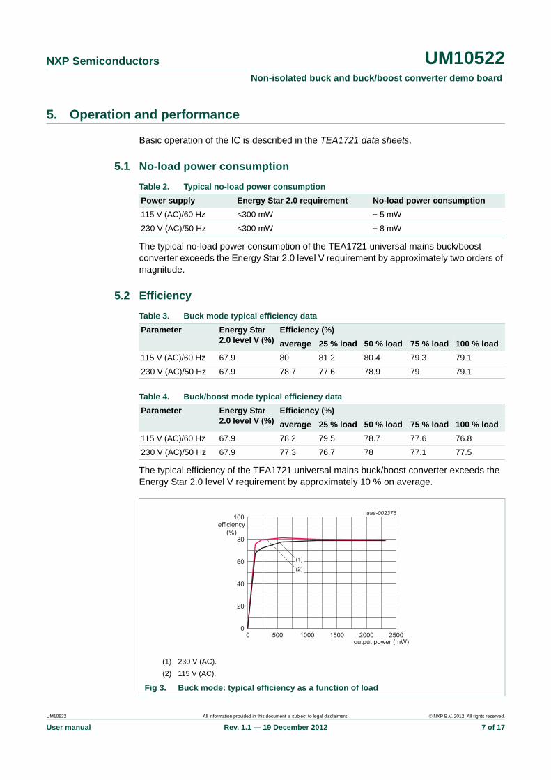
5. Operation and performance
Basic operation of the IC is described in the TEA1721 data sheets.
5.1 No-load power consumption
The typical no-load power consumption of the TEA1721 universal mains buck/boost converter exceeds the Energy Star 2.0 level V requirement by approximately two orders of magnitude.
5.2 Efficiency
The typical efficiency of the TEA1721 universal mains buck/boost converter exceeds the Energy Star 2.0 level V requirement by approximately 10 % on average.
Table 2. Typical no-load power consumption
Power supply Energy Star 2.0 requirement No-load power consumption
115 V (AC)/60 Hz <300 mW 5 mW
230 V (AC)/50 Hz <300 mW 8 mW
Table 3. Buck mode typical efficiency data
Parameter Energy Star 2.0 level V (%)
Efficiency (%)
average 25 % load 50 % load 75 % load 100 % load
115 V (AC)/60 Hz 67.9 80 81.2 80.4 79.3 79.1
230 V (AC)/50 Hz 67.9 78.7 77.6 78.9 79 79.1
Table 4. Buck/boost mode typical efficiency data
Parameter Energy Star 2.0 level V (%)
Efficiency (%)
average 25 % load 50 % load 75 % load 100 % load
115 V (AC)/60 Hz 67.9 78.2 79.5 78.7 77.6 76.8
230 V (AC)/50 Hz 67.9 77.3 76.7 78 77.1 77.5
(1) 230 V (AC).
(2) 115 V (AC).
Fig 3. Buck mode: typical efficiency as a function of load
40
60
20
80
100efficiency
(%)
0
output power (mW)0 250020001000 1500500
aaa-002376
(2)
(1)
UM10522 All information provided in this document is subject to legal disclaimers. © NXP B.V. 2012. All rights reserved.
User manual Rev. 1.1 — 19 December 2012 7 of 17

NXP Semiconductors UM10522Non-isolated buck and buck/boost converter demo board
5.3 Output voltage stability
(1) 115 V (AC).
(2) 230 V (AC).
Fig 4. Buck/boost mode: Typical efficiency as a function of load
Pout (mW)0 250020001000 1500500
aaa-002225
40
60
20
80
100
η(%)
0
(1) (2)
Fig 5. Buck mode: typical output voltage stability as a function of load
10
13
12
11
14outputvoltage
(V)
output power (mW)0 250020001000 1500500
aaa-002377
UM10522 All information provided in this document is subject to legal disclaimers. © NXP B.V. 2012. All rights reserved.
User manual Rev. 1.1 — 19 December 2012 8 of 17

NXP Semiconductors UM10522Non-isolated buck and buck/boost converter demo board
(1) 115 V (AC).
(2) 230 V (AC).
Fig 6. Buck/boost mode: Typical output voltage stability as a function of load
-14
Pout (mW)
aaa-002226
-12
-11
-13
-10
Vout(V)
0 250020001000 1500500
(1) (2)
UM10522 All information provided in this document is subject to legal disclaimers. © NXP B.V. 2012. All rights reserved.
User manual Rev. 1.1 — 19 December 2012 9 of 17

NXP Semiconductors UM10522Non-isolated buck and buck/boost converter demo board
6. Test results
6.1 ElectroMagnetic Interference
The TEA1721 buck and buck/boost mode converter application meets the requirements of EN55022. There is a margin of at least 10 dB with respect to the formal limits.
a. EMI at 115 V (AC) input voltage and 2 W output at 80 % load.
b. 230 V (AC) input voltage and 2 W output at 80 % load.
Fig 7. Typical EMI patterns measured at 2 W load
UM10522 All information provided in this document is subject to legal disclaimers. © NXP B.V. 2012. All rights reserved.
User manual Rev. 1.1 — 19 December 2012 10 of 17

NXP Semiconductors UM10522Non-isolated buck and buck/boost converter demo board
7. Demo board schematic
Fig 8. TEA1721 buck converter SMPS circuit diagram
����������
���
�����
�
�
�
��
������
�
��
� �� �� � ��
�
�
��
�
����
���
���
��
������
���
�������
�� �
��
����
��� ��
���
Fig 9. TEA1721 buck/boost converter SMPS circuit diagram
����������
���
�����
�
�
�
��
������
�
��
� �� �� � ��
�
�
��
�
����
���
���
��
������
���
�������
�� �
��
����
��� ��
���
UM10522 All information provided in this document is subject to legal disclaimers. © NXP B.V. 2012. All rights reserved.
User manual Rev. 1.1 — 19 December 2012 11 of 17
NXP Semiconductors UM10522Non-isolated buck and buck/boost converter demo board
8. PCB components
[1] To set the output voltage with greater accuracy, fine-tuning is required.
Table 5. Demo board components
Reference Description and value Part number Manufacturer
C1 electrolytic capacitor; 4.7 F; 400 V - -
C2 electrolytic capacitor; 4.7 F; 400 V - -
C3 capacitor; 10 pF; 25 V - -
C4 capacitor; 100 nF; 50 V - -
C5 electrolytic capacitor; 10 F; 35 V - -
C6 electrolytic capacitor; 470 F; 16 V - -
C7 capacitor; 100 nF; 50 V - -
D1 diode; S1M; SMA - -
D2 diode; BZG03-C200; optional see text; SMA BZG03-C200 -
D3 diode; BZG03-C200; optional see text; SMA BZG03-C200 -
D4 diode; ES1JL; SMF - -
D5 diode; BYG20J; SMA BYG20J -
D6 diode; ES1JL; SMF - -
D7 diode; BZX384-B12; SOD323 BZX384-B12 NXP Semiconductors
IC1 TEA1721; SO7 - NXP Semiconductors
JP1 jumper; 0 ; must be installed for buck/boost mode operation
- -
JP2 jumper; 0 installed; must be installed for buck mode only operation
- -
L1 1 mH; 80 mA - -
L2 1 mH; 250 mA (RMS); Isat = 500 mA - -
R1 carbon resistor; 47 - -
R2 resistor; 4.7 k; 1 % - -
R3 resistor; 18 k; 1 %[1] - -
R4 resistor; 1 ; 0.25 W - -
R5 resistor; 68 k - -
UM10522 All information provided in this document is subject to legal disclaimers. © NXP B.V. 2012. All rights reserved.
User manual Rev. 1.1 — 19 December 2012 12 of 17

NXP Semiconductors UM10522Non-isolated buck and buck/boost converter demo board
9. Implementation guidelines
• The output voltage is adjusted using resistors R2 and R3. In Buck mode, the converter can be used to generate an output voltage between +12 V (DC) and +32 V (DC). In buck/boost mode, the output voltage is between 12 V (DC) and 32 V (DC).
• The maximum output power and output current levels are adjusted using resistor R4. The maximum current allowed in the TEA1721 IC switching MOSFET is 700 mA. Take care that under no circumstance, the peak current in inductor L2 exceeds 700 mA.
• Resistor R1 limits the inrush current. The resistor must be a carbon resistor because metal film resistors can act as a fuse in this position. If no inrush current limiting is required, the resistor can be replaced with a short-circuit.
• EMI filtering is implemented using a single differential stage (C1-L1-C2). Mount additional film capacitors in parallel with C1 and C2 for improved HF noise suppression.
• Surge voltage protection is implemented using TVS diodes D2 and D3. The surge protection limits the DC bus voltage to 400 V maximum. The TVS diodes choice determines the maximum allowable surge pulse energy. The surge protection feature is optional. When not needed diodes D2 and D3 can be eliminated
• To cope with negative voltage surge pulses, diode D1 must be capable of handling a certain amount of avalanche surge energy. The presence of resistor R1 helps to limit any avalanche surge current in diode D1.
• Capacitors C4 and C5 can be replaced with a single (SMD) 2.2 F ceramic capacitor with the appropriate voltage rating. Though more expensive, it needs less board space.
• Resistor R5 forms a small pre-load for the converter. When the output voltages are adjusted, also adjust the pre-load resistors to ensure that they consume roughly the same amount of power. Depending on the connected load, the pre-load resistor can be eliminated.
• Zener diode D7 is an elementary output OverVoltage Protection (OVP). When OVP is not needed, eliminate the diode.
• Capacitor C7 is used to obtain additional (HF) voltage stability and noise suppression. Eliminate the capacitor when the feature is not needed.
UM10522 All information provided in this document is subject to legal disclaimers. © NXP B.V. 2012. All rights reserved.
User manual Rev. 1.1 — 19 December 2012 13 of 17

NXP Semiconductors UM10522Non-isolated buck and buck/boost converter demo board
10. Board layout
The 34.3 mm 34.3 mm evaluation PCB accommodates either a TEA1721 buck or buck/boost mode application implementation. This board can be used for the particular application shown in the circuit diagram and the associated component list.
The bottom silk screen is normally not used in PCB production. Merged with the bottom copper, it is shown here as a component placement reference only. Populate all component positions in this application. See Table 5 for a list of components.
a. Top silk screen plus top component placement and drill pattern
b. Bottom copper and bottom silk screen plus component placement
Fig 10. PCB layout
Table 6. Drill tool table
Drill tool code Drill diameter
C 1 mm
D 0.9 mm
E 1.3 mm
UM10522 All information provided in this document is subject to legal disclaimers. © NXP B.V. 2012. All rights reserved.
User manual Rev. 1.1 — 19 December 2012 14 of 17

NXP Semiconductors UM10522Non-isolated buck and buck/boost converter demo board
11. References
[1] TEA1721XT - Ultra-low standby SMPS controller with integrated power switch
[2] AN11060 - TEA172X 5 W to 11 W power supply/USB charger
UM10522 All information provided in this document is subject to legal disclaimers. © NXP B.V. 2012. All rights reserved.
User manual Rev. 1.1 — 19 December 2012 15 of 17

NXP Semiconductors UM10522Non-isolated buck and buck/boost converter demo board
12. Legal information
12.1 Definitions
Draft — The document is a draft version only. The content is still under internal review and subject to formal approval, which may result in modifications or additions. NXP Semiconductors does not give any representations or warranties as to the accuracy or completeness of information included herein and shall have no liability for the consequences of use of such information.
12.2 Disclaimers
Limited warranty and liability — Information in this document is believed to be accurate and reliable. However, NXP Semiconductors does not give any representations or warranties, expressed or implied, as to the accuracy or completeness of such information and shall have no liability for the consequences of use of such information. NXP Semiconductors takes no responsibility for the content in this document if provided by an information source outside of NXP Semiconductors.
In no event shall NXP Semiconductors be liable for any indirect, incidental, punitive, special or consequential damages (including - without limitation - lost profits, lost savings, business interruption, costs related to the removal or replacement of any products or rework charges) whether or not such damages are based on tort (including negligence), warranty, breach of contract or any other legal theory.
Notwithstanding any damages that customer might incur for any reason whatsoever, NXP Semiconductors’ aggregate and cumulative liability towards customer for the products described herein shall be limited in accordance with the Terms and conditions of commercial sale of NXP Semiconductors.
Right to make changes — NXP Semiconductors reserves the right to make changes to information published in this document, including without limitation specifications and product descriptions, at any time and without notice. This document supersedes and replaces all information supplied prior to the publication hereof.
Suitability for use — NXP Semiconductors products are not designed, authorized or warranted to be suitable for use in life support, life-critical or safety-critical systems or equipment, nor in applications where failure or malfunction of an NXP Semiconductors product can reasonably be expected to result in personal injury, death or severe property or environmental damage. NXP Semiconductors and its suppliers accept no liability for inclusion and/or use of NXP Semiconductors products in such equipment or applications and therefore such inclusion and/or use is at the customer’s own risk.
Applications — Applications that are described herein for any of these products are for illustrative purposes only. NXP Semiconductors makes no representation or warranty that such applications will be suitable for the specified use without further testing or modification.
Customers are responsible for the design and operation of their applications and products using NXP Semiconductors products, and NXP Semiconductors accepts no liability for any assistance with applications or customer product design. It is customer’s sole responsibility to determine whether the NXP Semiconductors product is suitable and fit for the customer’s applications and products planned, as well as for the planned application and use of customer’s third party customer(s). Customers should provide appropriate design and operating safeguards to minimize the risks associated with their applications and products.
NXP Semiconductors does not accept any liability related to any default, damage, costs or problem which is based on any weakness or default in the customer’s applications or products, or the application or use by customer’s third party customer(s). Customer is responsible for doing all necessary testing for the customer’s applications and products using NXP Semiconductors products in order to avoid a default of the applications and the products or of the application or use by customer’s third party customer(s). NXP does not accept any liability in this respect.
Export control — This document as well as the item(s) described herein may be subject to export control regulations. Export might require a prior authorization from competent authorities.
Evaluation products — This product is provided on an “as is” and “with all faults” basis for evaluation purposes only. NXP Semiconductors, its affiliates and their suppliers expressly disclaim all warranties, whether express, implied or statutory, including but not limited to the implied warranties of non-infringement, merchantability and fitness for a particular purpose. The entire risk as to the quality, or arising out of the use or performance, of this product remains with customer.
In no event shall NXP Semiconductors, its affiliates or their suppliers be liable to customer for any special, indirect, consequential, punitive or incidental damages (including without limitation damages for loss of business, business interruption, loss of use, loss of data or information, and the like) arising out the use of or inability to use the product, whether or not based on tort (including negligence), strict liability, breach of contract, breach of warranty or any other theory, even if advised of the possibility of such damages.
Notwithstanding any damages that customer might incur for any reason whatsoever (including without limitation, all damages referenced above and all direct or general damages), the entire liability of NXP Semiconductors, its affiliates and their suppliers and customer’s exclusive remedy for all of the foregoing shall be limited to actual damages incurred by customer based on reasonable reliance up to the greater of the amount actually paid by customer for the product or five dollars (US$5.00). The foregoing limitations, exclusions and disclaimers shall apply to the maximum extent permitted by applicable law, even if any remedy fails of its essential purpose.
12.3 TrademarksNotice: All referenced brands, product names, service names and trademarks are the property of their respective owners.
UM10522 All information provided in this document is subject to legal disclaimers. © NXP B.V. 2012. All rights reserved.
User manual Rev. 1.1 — 19 December 2012 16 of 17
NXP Semiconductors UM10522Non-isolated buck and buck/boost converter demo board
13. Contents
1 Introduction . . . . . . . . . . . . . . . . . . . . . . . . . . . . 31.1 Features and benefits . . . . . . . . . . . . . . . . . . . . 3
2 Safety Warning. . . . . . . . . . . . . . . . . . . . . . . . . . 3
3 Specification. . . . . . . . . . . . . . . . . . . . . . . . . . . . 4
4 Demo board connections . . . . . . . . . . . . . . . . . 6
5 Operation and performance . . . . . . . . . . . . . . . 75.1 No-load power consumption. . . . . . . . . . . . . . . 75.2 Efficiency . . . . . . . . . . . . . . . . . . . . . . . . . . . . . 75.3 Output voltage stability . . . . . . . . . . . . . . . . . . . 8
6 Test results . . . . . . . . . . . . . . . . . . . . . . . . . . . . 106.1 ElectroMagnetic Interference . . . . . . . . . . . . . 10
7 Demo board schematic . . . . . . . . . . . . . . . . . . 11
8 PCB components . . . . . . . . . . . . . . . . . . . . . . . 12
9 Implementation guidelines . . . . . . . . . . . . . . . 13
10 Board layout. . . . . . . . . . . . . . . . . . . . . . . . . . . 14
11 References . . . . . . . . . . . . . . . . . . . . . . . . . . . . 15
12 Legal information. . . . . . . . . . . . . . . . . . . . . . . 1612.1 Definitions. . . . . . . . . . . . . . . . . . . . . . . . . . . . 1612.2 Disclaimers . . . . . . . . . . . . . . . . . . . . . . . . . . . 1612.3 Trademarks. . . . . . . . . . . . . . . . . . . . . . . . . . . 16
13 Contents . . . . . . . . . . . . . . . . . . . . . . . . . . . . . . 17
© NXP B.V. 2012. All rights reserved.
For more information, please visit: http://www.nxp.comFor sales office addresses, please send an email to: [email protected]
Date of release: 19 December 2012
Document identifier: UM10522
Please be aware that important notices concerning this document and the product(s)described herein, have been included in section ‘Legal information’.