ultra low power boost converter charger energy … · user's guide sluu654a–october...
TRANSCRIPT

User's GuideSLUU654A–October 2011–Revised October 2011
bq25504 EVM – Ultra Low Power Boost Converter withBattery Management for Energy Harvester Applications
This user’s guide describes the bq25504 evaluation module (EVM), how to perform a stand-aloneevaluation and allows the EVM to interface with the system and host. This EVM is programmed from thefactory for settings compatible with most MCU’s and 3V coin cell batteries. The EVM is programmed todeliver a 3.1VDC maximum voltage (OV) for charging the storage element and the under voltage isprogrammed to 2.2VDC. The VBAT_OK indicator toggles high when VSTOR ramps up to 2.8VDC andtoggles low when VSTOR ramps down to 2.4VDC.
Contents1 Introduction .................................................................................................................. 2
1.1 EVM Features ...................................................................................................... 21.2 General Description ................................................................................................ 21.3 Design and Evaluation Considerations .......................................................................... 3
2 Performance Specification Summary ..................................................................................... 43 Test Summary ............................................................................................................... 4
3.1 Equipment ........................................................................................................... 43.2 Equipment and EVM Setup ....................................................................................... 43.3 Test procedures .................................................................................................... 5
4 PCB Layout Guideline .................................................................................................... 115 Bill of Materials, Board Layout and Schematics ....................................................................... 12
5.1 Bill of Materials .................................................................................................... 125.2 EVM Board Layout ............................................................................................... 135.3 EVM Schematic ................................................................................................... 15
List of Figures
1 Test Setup for HPA674A (bq25504 EVM) ............................................................................... 5
2 Startup with no Battery and 10k Load.................................................................................... 6
3 Startup with Battery Less Than UV....................................................................................... 7
4 Powering up with a Battery above UV ................................................................................... 7
5 BAT_OK High/Low 2.8V/2.34V – Ramping Battery from 0V to 3.1V (OV) and Down to 1.8V. ................... 8
6 Basic Switching Converter, Vin = 1V, Vbat = 2.5V ..................................................................... 9
7 EVM Operation Near OV With 100-Ω Battery Impedance ........................................................... 10
8 EVM PCB Top Assembly................................................................................................. 13
9 EVM PCB Top Layer ..................................................................................................... 13
10 EVM PCB Bottom Layer .................................................................................................. 14
11 EVM Schematic............................................................................................................ 15
List of Tables
1 I/O Connections and Configuration for Evaluation of bq25504 EVM................................................. 4
2 Bill of Materials............................................................................................................. 12
1SLUU654A–October 2011–Revised October 2011 bq25504 EVM – Ultra Low Power Boost Converter with Battery Management forEnergy Harvester ApplicationsSubmit Documentation Feedback
Copyright © 2011, Texas Instruments Incorporated

Introduction www.ti.com
1 Introduction
1.1 EVM Features• Evaluation module for bq25504
• Ultra low power boost converter/charger with battery management for energy harvester applications
• Resistor-programmable settings for under voltage, over voltage providing flexible battery management;POTs Included for fine tuning the settings (not populated)
• Programmable push-pull output Indicator for battery status (VBAT_OK)
• Test points for key signals available for testing purpose – easy probe hook-up.
• Jumpers available – easy to change settings
1.2 General Description
The bq25504 is the first of a new family of intelligent integrated energy harvesting Nano-Powermanagement solutions that are well suited for meeting the special needs of ultra low power applications.The product is specifically designed to efficiently acquire and manage the microwatts (µW) to miliwatts(mW) of power generated from a variety of DC sources like photovoltaic (solar) or thermal electricgenerators. The bq25504 is the first device of its kind to implement a highly efficient boostconverter/charger targeted toward products and systems, such as wireless sensor networks (WSN) whichhave stringent power and operational demands. The design of the bq25504 starts with a DC-DC boostconverter/charger that requires only microwatts of power to begin operating. Once started, the boostconverter/charger can effectively extract power from low voltage output harvesters such as thermoelectricgenerators (TEGs) or single / dual cell solar panels. The boost converter can be started with VIN as lowas 330 mV typ., and once started, can continue to harvest energy down to VIN ≃ 100 mV.
The bq25504 also implements a programmable maximum power point tracking (MPPT) sampling networkto optimize the transfer of power into the device. The MPP is listed by the harvesting manufacturer as apercentage of its open circuit (OC) voltage. Typically solar cells are at their MPP when loaded to ~80% oftheir OC voltage. The bq25504 periodically samples the open circuit input voltage by disabling the boostconverter (approximately every 16 seconds) and stores the programmed MPP ratio of the OC voltage onthe external reference capacitor, C5. If the storage element is less than the maximum voltage (OV) thenthe boost converter will load the harvesting source until it reaches the MPP (C5 voltage reference) andthen regulate the input voltage of the converter, thus transferring the maximum amount of power to theoutput. Alternatively, an external reference voltage can be provided, by a MCU to the REFS pin, to adjustC5 independently. The shunt on JP1 has to be moved from the Divider setting to STOR when providingthis external reference (JP1-2 tied to JP1-1 – OSC/STOR).
The bq25504 was designed with the flexibility to support a variety of energy storage elements. Theavailability of the sources from which harvesters extract their energy can often be sporadic ortime-varying. Systems will typically need some type of energy storage element, such as a re-chargeablebattery, super capacitor, or conventional capacitor. The storage element will make certain constant poweris available when needed for the systems. The storage element also allows the system to handle any peakcurrents that can not directly come from the input source.
To prevent damage to a customer’s storage element, both maximum and minimum voltages are monitoredagainst the user programmed under-voltage (UV) and over-voltage (OV) levels.
To further assist users in the strict management of their energy budgets, the bq25504 toggles the batterygood flag to signal the microprocessor when the voltage on an energy storage element or capacitor hasdropped below a pre-set critical level. This should trigger the shedding of load currents to prevent thesystem from entering an under voltage condition.
The OV, UV and battery good thresholds are programmed independently. The EVM has three 500KΩpotentiometers (not installed at factory) to allow fine tuning of the three programmable thresholds. Thisonly need be done if the user needs precision, the POTs provide about ±50mV shift.
For details, see bq25504 data sheet (SLUSAH0).
2 bq25504 EVM – Ultra Low Power Boost Converter with Battery Management for SLUU654A–October 2011–Revised October 2011Energy Harvester Applications Submit Documentation Feedback
Copyright © 2011, Texas Instruments Incorporated

R1
D1C A
BAT+
GND
www.ti.com Introduction
1.3 Design and Evaluation Considerations
This user's guide is not a replacement for the data sheet. Reading the data sheet first will help inunderstanding the operations and features of this IC. Be sure to make note of the capacitor selectionsection when designing the EVM. Many of the IC's pin names start with a "V" and this "V" is removed onthe EVM connector's label. The names are interchangeable.
This IC is a highly efficient charger for a storage element such as a battery or super capacitor. In thisdocument, “battery” will be used but one could substitute any appropriate storage element. The maindifference between a battery and a super capacitor is the capacity curve. The battery typically has little orno capacity below a certain voltage, where as the capacitor does have capacity at lower voltages.
In the lab when using a lab power supply rather than an energy harvester, one will have the output of thelab supply, Vsource, followed by the harvester's impedance (about 20Ω) and connected to VIN of the EVM.These two signals are separated by the 20Ω source impedance which represents the internal impedanceof the source. VIN is equal to VSource when there is no load (open circuit) and is pulled down to the MPPTharvester threshold when the charger is able to deliver the maximum power before reaching OV.
The over voltage (OV) setting initially is lower than the programmed value at startup (varies on conditions)and is updated after the first ~32ms. Subsequent updates are every ~64ms. The OV threshold is thereference for maximum voltage on VSTOR and the boost converter will stop switching if the voltage onVSTOR reaches the OV reference. The UV is checked every ~64ms to determine if the BAT FET shouldbe on or off. The open circuit (OC) input voltage is measured every ~16 seconds which is used tocalculate the Maximum Power Point Tracking (MPPT) threshold (programmed with resistors to 78% at thefactory). This periodic update continually optimizes maximum power delivery based on the harvestingconditions.
Harvesting ultra low power energy requires a different mind set when designing a system. Often there isnot enough real time input harvested power to run the system in full operation so energy is collected overa period of time, stored in a battery and then used periodically to power the system.
The designer needs to define a “Battery OK” threshold and battery discharged threshold (Not OK) to allowsuccessful system operation. The BAT_OK high/low threshold are programmed at the factory to 2.8V and2.4V using resistors R7, R8, and R9. A BAT_OK high signal would typically indicate to the host that thebattery is above 2.8V and ready to use and if low would indicate that the cell is discharged such that thesystem load should be reduced or disabled. The BAT_OK signal is checked every 64ms.
The quiescent current, which is basically the current from the battery to the IC, can be measured at theSTOR pin. To measure the current the user should connect a 100kΩ resistor to J5-2 (STOR) and connecta 3V supply from the other end of this resistor to the ground of the EVM. A 10MΩ meter can be used tomeasure the voltage drop across the resistor and calculate the current. No other connections should bemade to the EVM and the measurement should be taken after steady state conditions are reached (maytake a few minutes). The reading should be in the range of 375nA.
The battery (storage element) can be replaced with a simulated battery. Often electronic 4 quadrant loadsgive erratic results with a “battery charger” due to the charger changing states (fast-charge to terminationand refresh) while the electronic load is changing loads to maintain the “battery” voltage. The charging andloading get out of phase and creates a large signal oscillation which is due to the 4 quadrant meter. Asimple circuit can be used to simulate a battery and works well and can quickly be adjusted for voltage. Itconsists of load resistor (~10Ω, 2W) to pull the output down to some minimum storage voltage (sinkingcurrent part of battery) and a lab supply connected to the BAT pin via a diode. The lab supply biases upthe battery voltage to the desired level. It may be necessary to add more capacitance across R1.
3SLUU654A–October 2011–Revised October 2011 bq25504 EVM – Ultra Low Power Boost Converter with Battery Management forEnergy Harvester ApplicationsSubmit Documentation Feedback
Copyright © 2011, Texas Instruments Incorporated

Performance Specification Summary www.ti.com
2 Performance Specification Summary
See Data Sheet “Recommended Operating Conditions” for component adjustments. For details about theresistor programmable settings, see bq25504 data sheet (SLUSAH0).
MIN NOM MAX UNIT
VIN(DC) DC input voltage into VIN_DC 0.13 3.0 V
VIN_Start-up(DC) DC minimum Start-up Voltage 330 mV
VOV Over Voltage – Sets maximum output voltage 2.9 3.1 3.3 V
VUV Under voltage setting for shorting VSTOR to VBAT 2.1 2.2 2.3 V
VBAT_OK indication toggles high when VSTOR ramps up 2.65 2.8 2.95 VVBAT_OK
VBAT_OK indication toggles low when VSTOR ramps down 2.25 2.4 2.55 V
MPPT Maximum Power Point Tracking, Programmed % of Open Circuit Voltage 78%
CBAT Battery Pin Capacitance or equivalent battery capacity 100 µF
3 Test Summary
3.1 Equipment
Power SuppliesPower Supply #1 (PS#1): Adjustable 5V Power supply with Current Limit of 100mA.Power Supply #2 (PS#2): Adjustable 5V Power supply with 20Ω series impedance (can just be a discreteresistor) with Current Limit of 100mA.
LoadsLoad #1: 10kΩ, 5%, 0.25W resistor and 1kΩ, 5%, 0.25W resistor as per procedure P/S#2 seriesresistance: 20Ω, 5%, 0.25W
MetersMeter#1,2,3: Fluke 75 multi-meter, (equivalent or better) for voltage measurements
ScopeStandard scope with at least two channels
3.2 Equipment and EVM Setup
Table 1. I/O Connections and Configuration for Evaluation of bq25504 EVM
Jack Description Factory Setting
J1–VIN Input Source (+)
J1–GND Input Source Return (–)
J2–BAT Battery connection (+)
J2–GND Battery Connection Return (–)
J3 – VIN Input Source Sense (+) [for J1]
J3 -GND Input Source Return Sense (–) [for J1]
J4 – BAT_OK Battery Status Indicator (+)
J4 - GND Battery Status Indicator Return (–)
J5 – STOR Charger Output (+)
J5 – GND Charger Output Return (–)
J6 – STOR Charger Output Sense (+)
J6 – BAT Battery Connection Sense (+) [for J2]
J6 - GND Battery Connection Sense (–) [for J2]
JP1 MPPT setting: Enabled-Divider; Disabled-STOR Place Shunt on JP1-2/3 (Divider)
JP2 OCS Setting: C5 Capacitor-No Shunt; Disabled-Shunt on REF-GND No Shunt(JP1 should be Disabled)
4 bq25504 EVM – Ultra Low Power Boost Converter with Battery Management for SLUU654A–October 2011–Revised October 2011Energy Harvester Applications Submit Documentation Feedback
Copyright © 2011, Texas Instruments Incorporated
Meter # 2
- +
Meter # 1
+ -
Meter # 3
+
- +
P/S # 1
Load # 1
_
Meter # 4
+
Jumper
Meter # 2
- +
Meter # 1
Meter # 3
-
- +
P/S # 1
Load # 1
_
Meter # 4
+
Jumper
www.ti.com Test Summary
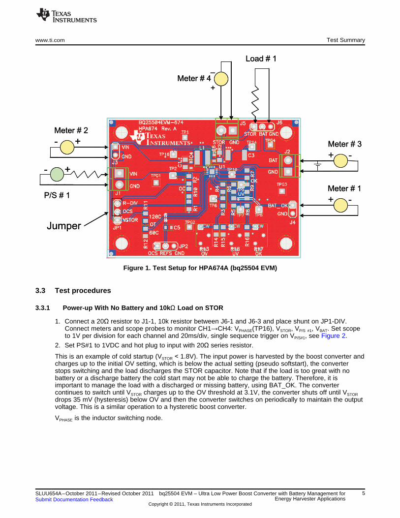
Figure 1. Test Setup for HPA674A (bq25504 EVM)
3.3 Test procedures
3.3.1 Power-up With No Battery and 10kΩ Load on STOR
1. Connect a 20Ω resistor to J1-1, 10k resistor between J6-1 and J6-3 and place shunt on JP1-DIV.Connect meters and scope probes to monitor CH1→CH4: VPHASE(TP16), VSTOR, VP/S #1, VBAT. Set scopeto 1V per division for each channel and 20ms/div, single sequence trigger on VP/S#1, see Figure 2.
2. Set PS#1 to 1VDC and hot plug to input with 20Ω series resistor.
This is an example of cold startup (VSTOR < 1.8V). The input power is harvested by the boost converter andcharges up to the initial OV setting, which is below the actual setting (pseudo softstart), the converterstops switching and the load discharges the STOR capacitor. Note that if the load is too great with nobattery or a discharge battery the cold start may not be able to charge the battery. Therefore, it isimportant to manage the load with a discharged or missing battery, using BAT_OK. The convertercontinues to switch until VSTOR charges up to the OV threshold at 3.1V, the converter shuts off until VSTOR
drops 35 mV (hysteresis) below OV and then the converter switches on periodically to maintain the outputvoltage. This is a similar operation to a hysteretic boost converter.
VPHASE is the inductor switching node.
5SLUU654A–October 2011–Revised October 2011 bq25504 EVM – Ultra Low Power Boost Converter with Battery Management forEnergy Harvester ApplicationsSubmit Documentation Feedback
Copyright © 2011, Texas Instruments Incorporated

Vphase
Vstor
Vbat
Vp/s#1
Test Summary www.ti.com
Figure 2. Startup with no Battery and 10k Load
3.3.2 Power-up with Battery less than UV (less than a diode drop below UV)
1. Same setup, as 3.3.1, except move the probe on VBAT to VIN and apply a charge element set to 1.9VDCbetween BAT and GND. Arm scope to trigger on VP/S #1.
2. Set PS#1 to 1VDC and hot plug to input with 20Ω series resistor, see Figure 3.
The start up is similar to the case without the battery but after the initial ~40ms period the STOR chargesto 2.8V or ~0.9V above the battery and is charging the element via the BAT FET body diode. The nextsampling cycle for UV detects that the VSTOR is greater than UV (2.2V) and then turns on the BAT FET.Since the battery is at 1.9V, VSTOR is pulled down to ~1.9V and the next UV sampling turns off the BATFET. The cycling continues until the battery gets charged to the UV threshold and then finally the BATFET stays on. A less complicated design would turn off the system load once the battery drops near theUV threshold to avoid this cycling.
If the storage element is lower than the maximum voltage (OV) then the element can theoretically take allof the available input power. As the harvesting source is loaded, its output voltage drops until reaching theMPPT threshold, which is currently programmed to 78% of the OC voltage and then the boost converterregulates the input voltage at this level by controlling the power transferred to the load. Note how Vinregulates to 78% of P/S#1 when the battery is lower than the OV voltage. Vary the input voltage slightlyand wait for the 16 second update cycle to see how the MPPT is updated.
For a battery that is more than a diode drop below 1.8V, the charger may get stuck in cold startup which isless efficient and would take longer to recover. Once the STOR voltage gets above 1.8V and more than32ms after power is applied, the low power cold start circuit is disabled and the main boost convertertakes over.
6 bq25504 EVM – Ultra Low Power Boost Converter with Battery Management for SLUU654A–October 2011–Revised October 2011Energy Harvester Applications Submit Documentation Feedback
Copyright © 2011, Texas Instruments Incorporated

Vphase
Vstor
Vp/s#1Vin
Vphase
Vp/s#1Vin
Vstor
www.ti.com Test Summary
Figure 3. Startup with Battery Less Than UV
3.3.3 Power-up with Battery more than UV (2.3V to 3V), BAT FET ON
1. Same setup as 3.3.1, except change the charge element set to 2.4VDC between BAT and GND. Setscope to 2sec/div and to roll.
2. Set PS#1 to 1VDC and hot plug to input with 10Ω series resistor, see Figure 4.
Note in Figure 4 that the BAT FET is on and the STOR output is powered prior to the input being applied.This means the converter will start up in normal boost mode and after doing its initial sampling willregulate VIN to the MPPT threshold.
Figure 4. Powering up with a Battery above UV
7SLUU654A–October 2011–Revised October 2011 bq25504 EVM – Ultra Low Power Boost Converter with Battery Management forEnergy Harvester ApplicationsSubmit Documentation Feedback
Copyright © 2011, Texas Instruments Incorporated

VbatVstorV_BAT-OK
Vphase
Test Summary www.ti.com
3.3.4 BAT_OK Indication as Battery Charges/Discharges
1. Connect scope probes CHI→CH4: VPHASE(TP16), VSTOR, VBAT_OK, VBAT and vary charge element fromzero voltage to 3.15V and back down to 1.8V and observe the BAT_OK signal.
Initially P/S#1 is set to 1V and the battery is adjusted to OV (simulated battery), which clamps VSTOR to~0.5V (lower body diode drop due to lower current). As the battery voltage is swept higher one can seethe different phases discussed earlier. Once the output gets to ~2.8V the BAT_OK signal goes high. Notethat the BAT_OK signal goes low once the battery is discharged to ~2.34V.
This signal’s high and low threshold can be programmed by R7, R8 and R9 to give an indication to thehost when the battery is good (Signal high – has enough energy to complete the designed task) and whenthe battery is discharged (Signal low – system needs to be disabled or low power mode so the battery canrecharge).
Figure 5. BAT_OK High/Low 2.8V/2.34V – Ramping Battery from 0V to 3.1V (OV) and Down to 1.8V.
3.3.5 Basic PFM Switching Waveform, Vin = 1V, Vbat = 2.5V
1. Set up scope as follows: CHI→CH4: VPHASE(TP16), VSTOR, VP/S #1, VIN, 10µs/DIV.
8 bq25504 EVM – Ultra Low Power Boost Converter with Battery Management for SLUU654A–October 2011–Revised October 2011Energy Harvester Applications Submit Documentation Feedback
Copyright © 2011, Texas Instruments Incorporated

Vin
Vstor
Vsource
Vphase
www.ti.com Test Summary
Figure 6. Basic Switching Converter, Vin = 1V, Vbat = 2.5V
Note here that VIN is regulating at the MPPT threshold so the boost circuit is delivering the maximumpower that the source can deliver. The user can see after about 4 pulses that the switching waveformsstops which cause the inductor to go discontinuous and ring.
9SLUU654A–October 2011–Revised October 2011 bq25504 EVM – Ultra Low Power Boost Converter with Battery Management forEnergy Harvester ApplicationsSubmit Documentation Feedback
Copyright © 2011, Texas Instruments Incorporated

Vphase
Vin
Vstor
Vbat
Test Summary www.ti.com
3.3.6 Operation Near OV With 100-Ω Battery Impedance1. Connect scope probes CHI→CH4: VPH(TP16), VSTOR, VIN, VBAT; set VP/S#1 to 1.3 VDC and VBAT to 3.00
VDC. Connect the power sources with their respective source impedance to the EVM. VIN sourceimpedance should be 20Ω and the battery impedance should be 100Ω. Set VSTOR and VBAT to20mVDC/div and 3.135VDC offset (3.135VDC was the average VBAT [OV] measurement), 1 ms/div.Turn on sources.
2. The input source has enough energy to charge the VSTOR up to the OV setting; and. when the boostconverter stops switching VSTOR will discharge down to the battery’s cell voltage which is ~3V which isbelow the OV reset hysteresis. See Figure 7 for operation near OV. Note the hysteresis of VSTOR isaround 35mV here, but this can vary depending on the input, output voltage, the source and batteryimpedance, and the number of pulses for each operation period of the boost converter.
Figure 7. EVM Operation Near OV With 100-Ω Battery Impedance
10 bq25504 EVM – Ultra Low Power Boost Converter with Battery Management for SLUU654A–October 2011–Revised October 2011Energy Harvester Applications Submit Documentation Feedback
Copyright © 2011, Texas Instruments Incorporated

www.ti.com PCB Layout Guideline
4 PCB Layout Guideline1. As with all switching power supplies, the layout is an important step in the design, especially at high
peak currents and high switching frequencies. If the layout is not carefully done, the boostconverter/charger could show stability problems as well as EMI problems. Therefore, use wide andshort traces for the main current path and for the power ground paths. The input and output capacitor,as well as the inductor should be placed as close as possible to the IC.
2. The resistors that program the thresholds should be placed as close as possible to the input pins of theIC to minimize parasitic capacitance to less than 2pF.
3. To lay out the ground, it is recommended to use short traces as well, separated from the power groundtraces. This avoids ground shift problems, which can occur due to superimposition of power groundcurrent and control ground current. Assure that the ground traces are connected close to the deviceGND pins.
4. It is critical that the exposed thermal pad on the backside of the bq25504 package be soldered to thePCB ground. Make sure there are sufficient thermal vias right underneath the IC, connecting to theground plane on the other layers.
5. Decoupling capacitors for VSTOR, VBAT should make the interconnections to the any Load as shortas possible.
6. EVM layout can be used as guidance though a smaller layout is achievable.
11SLUU654A–October 2011–Revised October 2011 bq25504 EVM – Ultra Low Power Boost Converter with Battery Management forEnergy Harvester ApplicationsSubmit Documentation Feedback
Copyright © 2011, Texas Instruments Incorporated

Bill of Materials, Board Layout and Schematics www.ti.com
5 Bill of Materials, Board Layout and Schematics
5.1 Bill of Materials
Table 2. Bill of Materials
Count RefDes Value Description Size Part Number MFR
2 C1, C2** 4.7uF Capacitor, Ceramic, 10V, X5R, 10% 0805 GRM219R61A475KE19D Murata
1 C3** 100uF Capacitor, Ceramic, 6.3V, X5R, 20% 1812 GRM43SR60J107ME20L Murata
2 C4, C6 0.1uF Capacitor, Ceramic, 50V, X7R, 10% 0603 Std Std
1 C5** 0.01uF Capacitor, Ceramic, 50V, X7R, 10% 0603 GRM188R71H103KA01D Murata
3 J1, J2, J5 ED555/2DS Terminal Block, 2-pin, 6-A, 3.5mm 0.27 x 0.25 ED555/2DS OSTinch
2 J3, J4 PEC02SAAN Header, Male 2-pin, 100mil spacing, 0.100 inch x 2 PEC02SAAN Sullins
1 J6 PEC03SAAN Header, Male 3-pin, 100mil spacing, 0.100 inch x 3 PEC03SAAN Sullins
2 JP1, JP2 PEC03SAAN Header, Male 3-pin, 100mil spacing, 0.100 inch x 3 PEC03SAAN Sullins
1 L1 22uH Inductor, SMT, 0.8A, 360milliohm 0.153 x 0.153 LPS4018-223MLB Coilcraftinch
1 R1 10.0M Resistor, Chip, 1/10W, 1% 0805 CRCW080510M0FKEA Vishay
0 R11 Open Resistor, Chip, 1/10W, 1% 0805 Std Std
4 R12, R14, R15, 0 Resistor, Chip, 1/10W, 1% 0805 Std STDR16
0 R13, R17, R18 Open Potentiometer, 1/4 in. Cermet, 12-Turn, 0.25x0.17 3266W-504LF BournsTop-Adjust
3 R2, R6, R8 4.42M Resistor, Chip, 1/10W, 1% 0805 CRCW08054M42FKEA Vishay
1 R3 5.90M Resistor, Chip, 1/10W, 1% 0805 CRCW08055M90FKEA Vishay
1 R4 4.02M Resistor, Chip, 1/10W, 1% 0805 CRCW08054M02FKEA Vishay
2 R5, R10 5.60M Resistor, Chip, 1/10W, 1% 0805 CRCW08055M60FKEA Vishay
1 R7 1.43M Resistor, Chip, 1/10W, 1% 0805 CRCW08051M43FKEA Vishay
1 R9 4.22M Resistor, Chip, 1/10W, 1% 0805 CRCW08054M22FKEA Vishay
0 TP1, TP2, TP6, Open Test Point, O.032 Hole STD STDTP7, TP8, TP9,TP10, TP14,TP16, TPG1,TPG2, TPG3,TPG4
1 U1 BQ25504RGT IC, NanoAmpere Integrated Boost QFN-16 BQ25504RGT TIConverter/Charger
1 -- PCB, 1.8 In x 1.8 In x 0.031 In HPA674 Any
2 See Note 5 Shunt, 100-mil, Black 0.1 929950-00 3M
Notes: 1. These assemblies are ESD sensitive, ESD precautions shall be observed.
2. These assemblies must be clean and free from flux and all contaminants. Use of no clean flux is not acceptable.
3. These assemblies must comply with workmanship standards IPC-A-610 Class 2.
4. Ref designators marked with an asterisk ('**') cannot be substituted. All other components can be substituted with equivalent MFG's components.
5. Place shunt on JP1-2/3 (Divider) and JP2 (place on just one pin – ckt should be floating).
12 bq25504 EVM – Ultra Low Power Boost Converter with Battery Management for SLUU654A–October 2011–Revised October 2011Energy Harvester Applications Submit Documentation Feedback
Copyright © 2011, Texas Instruments Incorporated

TI
EXAS
NSTRUMENTS
www.ti.com Bill of Materials, Board Layout and Schematics
5.2 EVM Board Layout
Figure 8. EVM PCB Top Assembly
Figure 9. EVM PCB Top Layer
13SLUU654A–October 2011–Revised October 2011 bq25504 EVM – Ultra Low Power Boost Converter with Battery Management forEnergy Harvester ApplicationsSubmit Documentation Feedback
Copyright © 2011, Texas Instruments Incorporated

Bill of Materials, Board Layout and Schematics www.ti.com
Figure 10. EVM PCB Bottom Layer
14 bq25504 EVM – Ultra Low Power Boost Converter with Battery Management for SLUU654A–October 2011–Revised October 2011Energy Harvester Applications Submit Documentation Feedback
Copyright © 2011, Texas Instruments Incorporated
www.ti.com Bill of Materials, Board Layout and Schematics
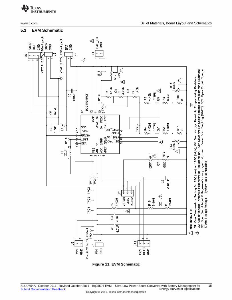
5.3 EVM Schematic
Figure 11. EVM Schematic
15SLUU654A–October 2011–Revised October 2011 bq25504 EVM – Ultra Low Power Boost Converter with Battery Management forEnergy Harvester ApplicationsSubmit Documentation Feedback
Copyright © 2011, Texas Instruments Incorporated

Evaluation Board/Kit Important Notice
Texas Instruments (TI) provides the enclosed product(s) under the following conditions:
This evaluation board/kit is intended for use for ENGINEERING DEVELOPMENT, DEMONSTRATION, OR EVALUATIONPURPOSES ONLY and is not considered by TI to be a finished end-product fit for general consumer use. Persons handling theproduct(s) must have electronics training and observe good engineering practice standards. As such, the goods being provided arenot intended to be complete in terms of required design-, marketing-, and/or manufacturing-related protective considerations,including product safety and environmental measures typically found in end products that incorporate such semiconductorcomponents or circuit boards. This evaluation board/kit does not fall within the scope of the European Union directives regardingelectromagnetic compatibility, restricted substances (RoHS), recycling (WEEE), FCC, CE or UL, and therefore may not meet thetechnical requirements of these directives or other related directives.
Should this evaluation board/kit not meet the specifications indicated in the User’s Guide, the board/kit may be returned within 30days from the date of delivery for a full refund. THE FOREGOING WARRANTY IS THE EXCLUSIVE WARRANTY MADE BYSELLER TO BUYER AND IS IN LIEU OF ALL OTHER WARRANTIES, EXPRESSED, IMPLIED, OR STATUTORY, INCLUDINGANY WARRANTY OF MERCHANTABILITY OR FITNESS FOR ANY PARTICULAR PURPOSE.
The user assumes all responsibility and liability for proper and safe handling of the goods. Further, the user indemnifies TI from allclaims arising from the handling or use of the goods. Due to the open construction of the product, it is the user’s responsibility totake any and all appropriate precautions with regard to electrostatic discharge.
EXCEPT TO THE EXTENT OF THE INDEMNITY SET FORTH ABOVE, NEITHER PARTY SHALL BE LIABLE TO THE OTHERFOR ANY INDIRECT, SPECIAL, INCIDENTAL, OR CONSEQUENTIAL DAMAGES.
TI currently deals with a variety of customers for products, and therefore our arrangement with the user is not exclusive.
TI assumes no liability for applications assistance, customer product design, software performance, or infringement ofpatents or services described herein.
Please read the User’s Guide and, specifically, the Warnings and Restrictions notice in the User’s Guide prior to handling theproduct. This notice contains important safety information about temperatures and voltages. For additional information on TI’senvironmental and/or safety programs, please contact the TI application engineer or visit www.ti.com/esh.
No license is granted under any patent right or other intellectual property right of TI covering or relating to any machine, process, orcombination in which such TI products or services might be or are used.
FCC Warning
This evaluation board/kit is intended for use for ENGINEERING DEVELOPMENT, DEMONSTRATION, OR EVALUATIONPURPOSES ONLY and is not considered by TI to be a finished end-product fit for general consumer use. It generates, uses, andcan radiate radio frequency energy and has not been tested for compliance with the limits of computing devices pursuant to part 15of FCC rules, which are designed to provide reasonable protection against radio frequency interference. Operation of thisequipment in other environments may cause interference with radio communications, in which case the user at his own expensewill be required to take whatever measures may be required to correct this interference.
EVM Warnings and Restrictions
It is important to operate this EVM within the input voltage range of 0 V to 5.5 V and the output voltage range of 0 V to 5.5 V .
Exceeding the specified input range may cause unexpected operation and/or irreversible damage to the EVM. If there arequestions concerning the input range, please contact a TI field representative prior to connecting the input power.
Applying loads outside of the specified output range may result in unintended operation and/or possible permanent damage to theEVM. Please consult the EVM User's Guide prior to connecting any load to the EVM output. If there is uncertainty as to the loadspecification, please contact a TI field representative.
During normal operation, some circuit components may have case temperatures greater than 60°C. The EVM is designed tooperate properly with certain components above 105°C as long as the input and output ranges are maintained. These componentsinclude but are not limited to linear regulators, switching transistors, pass transistors, and current sense resistors. These types ofdevices can be identified using the EVM schematic located in the EVM User's Guide. When placing measurement probes nearthese devices during operation, please be aware that these devices may be very warm to the touch.
Mailing Address: Texas Instruments, Post Office Box 655303, Dallas, Texas 75265Copyright © 2011, Texas Instruments Incorporated

IMPORTANT NOTICE
Texas Instruments Incorporated and its subsidiaries (TI) reserve the right to make corrections, modifications, enhancements, improvements,and other changes to its products and services at any time and to discontinue any product or service without notice. Customers shouldobtain the latest relevant information before placing orders and should verify that such information is current and complete. All products aresold subject to TI’s terms and conditions of sale supplied at the time of order acknowledgment.
TI warrants performance of its hardware products to the specifications applicable at the time of sale in accordance with TI’s standardwarranty. Testing and other quality control techniques are used to the extent TI deems necessary to support this warranty. Except wheremandated by government requirements, testing of all parameters of each product is not necessarily performed.
TI assumes no liability for applications assistance or customer product design. Customers are responsible for their products andapplications using TI components. To minimize the risks associated with customer products and applications, customers should provideadequate design and operating safeguards.
TI does not warrant or represent that any license, either express or implied, is granted under any TI patent right, copyright, mask work right,or other TI intellectual property right relating to any combination, machine, or process in which TI products or services are used. Informationpublished by TI regarding third-party products or services does not constitute a license from TI to use such products or services or awarranty or endorsement thereof. Use of such information may require a license from a third party under the patents or other intellectualproperty of the third party, or a license from TI under the patents or other intellectual property of TI.
Reproduction of TI information in TI data books or data sheets is permissible only if reproduction is without alteration and is accompaniedby all associated warranties, conditions, limitations, and notices. Reproduction of this information with alteration is an unfair and deceptivebusiness practice. TI is not responsible or liable for such altered documentation. Information of third parties may be subject to additionalrestrictions.
Resale of TI products or services with statements different from or beyond the parameters stated by TI for that product or service voids allexpress and any implied warranties for the associated TI product or service and is an unfair and deceptive business practice. TI is notresponsible or liable for any such statements.
TI products are not authorized for use in safety-critical applications (such as life support) where a failure of the TI product would reasonablybe expected to cause severe personal injury or death, unless officers of the parties have executed an agreement specifically governingsuch use. Buyers represent that they have all necessary expertise in the safety and regulatory ramifications of their applications, andacknowledge and agree that they are solely responsible for all legal, regulatory and safety-related requirements concerning their productsand any use of TI products in such safety-critical applications, notwithstanding any applications-related information or support that may beprovided by TI. Further, Buyers must fully indemnify TI and its representatives against any damages arising out of the use of TI products insuch safety-critical applications.
TI products are neither designed nor intended for use in military/aerospace applications or environments unless the TI products arespecifically designated by TI as military-grade or "enhanced plastic." Only products designated by TI as military-grade meet militaryspecifications. Buyers acknowledge and agree that any such use of TI products which TI has not designated as military-grade is solely atthe Buyer's risk, and that they are solely responsible for compliance with all legal and regulatory requirements in connection with such use.
TI products are neither designed nor intended for use in automotive applications or environments unless the specific TI products aredesignated by TI as compliant with ISO/TS 16949 requirements. Buyers acknowledge and agree that, if they use any non-designatedproducts in automotive applications, TI will not be responsible for any failure to meet such requirements.
Following are URLs where you can obtain information on other Texas Instruments products and application solutions:
Products Applications
Audio www.ti.com/audio Communications and Telecom www.ti.com/communications
Amplifiers amplifier.ti.com Computers and Peripherals www.ti.com/computers
Data Converters dataconverter.ti.com Consumer Electronics www.ti.com/consumer-apps
DLP® Products www.dlp.com Energy and Lighting www.ti.com/energy
DSP dsp.ti.com Industrial www.ti.com/industrial
Clocks and Timers www.ti.com/clocks Medical www.ti.com/medical
Interface interface.ti.com Security www.ti.com/security
Logic logic.ti.com Space, Avionics and Defense www.ti.com/space-avionics-defense
Power Mgmt power.ti.com Transportation and Automotive www.ti.com/automotive
Microcontrollers microcontroller.ti.com Video and Imaging www.ti.com/video
RFID www.ti-rfid.com
OMAP Mobile Processors www.ti.com/omap
Wireless Connectivity www.ti.com/wirelessconnectivity
TI E2E Community Home Page e2e.ti.com
Mailing Address: Texas Instruments, Post Office Box 655303, Dallas, Texas 75265Copyright © 2011, Texas Instruments Incorporated