ultra fine-grained run-time power gating of on-chip routers for cmps hiroki matsutani michihiro...
TRANSCRIPT
Ultra Fine-Grained Run-Time Power Gating of
On-Chip Routers for CMPs
Hiroki MatsutaniMichihiro KoibuchiDaisuke IkebuchiKimiyoshi UsamiHiroshi Nakamura Hideharu Amano
(Univ Tokyo, Japan)(NII, Japan)
(Keio Univ, Japan)(Shibaura IT, Japan)(Univ Tokyo, Japan)
(Keio Univ, Japan)

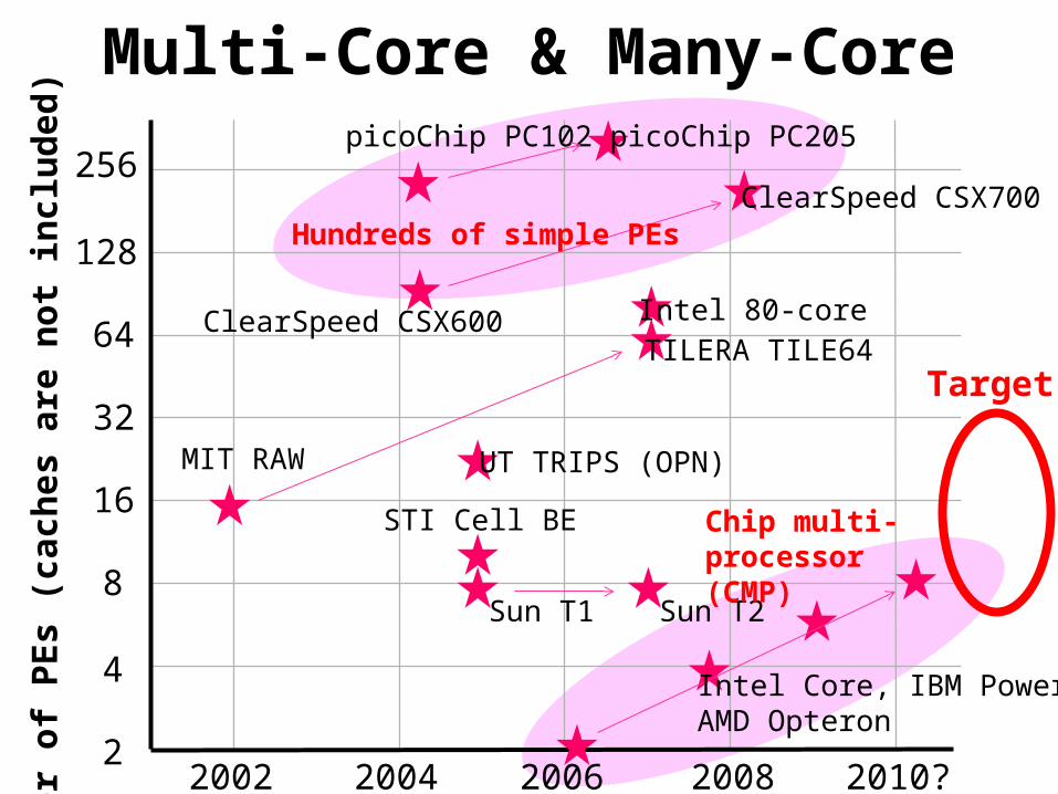
Multi-Core & Many-Core
4
8
16
32
64
128
256
2002 2004 2006 2008 2010?
MIT RAW
STI Cell BE
Sun T1 Sun T2
TILERA TILE64
Intel Core, IBM Power7AMD Opteron
Intel 80-coreClearSpeed CSX600
ClearSpeed CSX700
picoChip PC102 picoChip PC205
UT TRIPS (OPN)
Nu
mb
er
of
PEs (
cach
es a
re n
ot
inclu
ded
)
2
Multi-Core & Many-Core
4
8
16
32
64
128
256
2002 2004 2006 2008 2010?
MIT RAW
STI Cell BE
Sun T1 Sun T2
TILERA TILE64
Intel Core, IBM Power7AMD Opteron
Intel 80-coreClearSpeed CSX600
ClearSpeed CSX700
picoChip PC102 picoChip PC205
UT TRIPS (OPN)
Nu
mb
er
of
PEs (
cach
es a
re n
ot
inclu
ded
)
2
Hundreds of simple PEs
Chip multi-processor (CMP)
Target
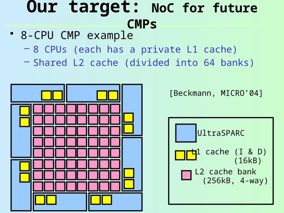
• 8-CPU CMP example– 8 CPUs (each has a private L1 cache)– Shared L2 cache (divided into 64 banks)
UltraSPARC
L1 cache (I & D)
L2 cache bank (16kB)
(256kB, 4-way)
[Beckmann, MICRO’04]
Our target: NoC for future CMPs

• 8-CPU CMP example– 8 CPUs (each has a private L1 cache)– Shared L2 cache (divided into 64 banks)– CPUs and cache banks are interconnected via NoC
On-chip router
UltraSPARC
L1 cache (I & D)
L2 cache bank (16kB)
(256kB, 4-way)
[Beckmann, MICRO’04]
On-chip network is an infrastructure of CMPs.
It must be always ready for the packet transfers.
It consumes leakage power at any time!
Run-time power gating that stops the power supply to the routers whenever possible is
required.
Our target: NoC for future CMPs
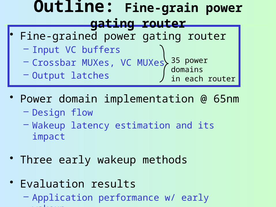
• Fine-grained power gating router– Input VC buffers– Crossbar MUXes, VC MUXes– Output latches
• Power domain implementation @ 65nm– Design flow– Wakeup latency estimation and its impact
• Three early wakeup methods
• Evaluation results– Application performance w/ early wakeup– Leakage power reduction
35 power domainsin each router
Outline: Fine-grain power gating router

• Coarse-grain approach– IP core (module) level– Surrounded by VGND– Power switch
between VGND and GND
• Fine-grain approach– Standard cell level– Each cell has VGND
port– All cells in a domain
share the same VGND line
Power gating: Coarse- vs. fine-grain
IP Core
GND ring
Virtual GND (VGND)
PowerSwitch
On/Off
IP Core IP CoreIP CoreIP CoreIP CoreIP CoreIP Core
[Usami, ICCD’06]

• Coarse-grain approach– IP core (module) level– Surrounded by VGND– Power switch
between VGND and GND
• Fine-grain approach– Standard cell level– Each cell has VGND
port– All cells in a domain
share the same VGND line
Power gating: Coarse- vs. fine-grain
IP Core
GND ring
Virtual GND (VGND)
PowerSwitch
On/Off
IP Core
OR AND
VDD
GND
INV DFF
GND
VDD
VGND
PowerSwitch
On/Off
[Usami, ICCD’06]
OR AND
VDD
GND
INV DFF
GND
VDD
OR AND
VDD
GND
INV DFF
GND
VDD
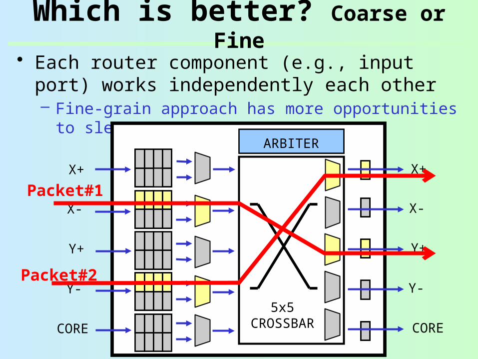
• Each router component (e.g., input port) works independently each other– Fine-grain approach has more opportunities to
sleepARBITER
X+
X-
Y+
Y-
CORE
X+
X-
Y+
Y-
CORE
5x5 CROSSBAR
Which is better? Coarse or Fine
Packet#2
Packet#1
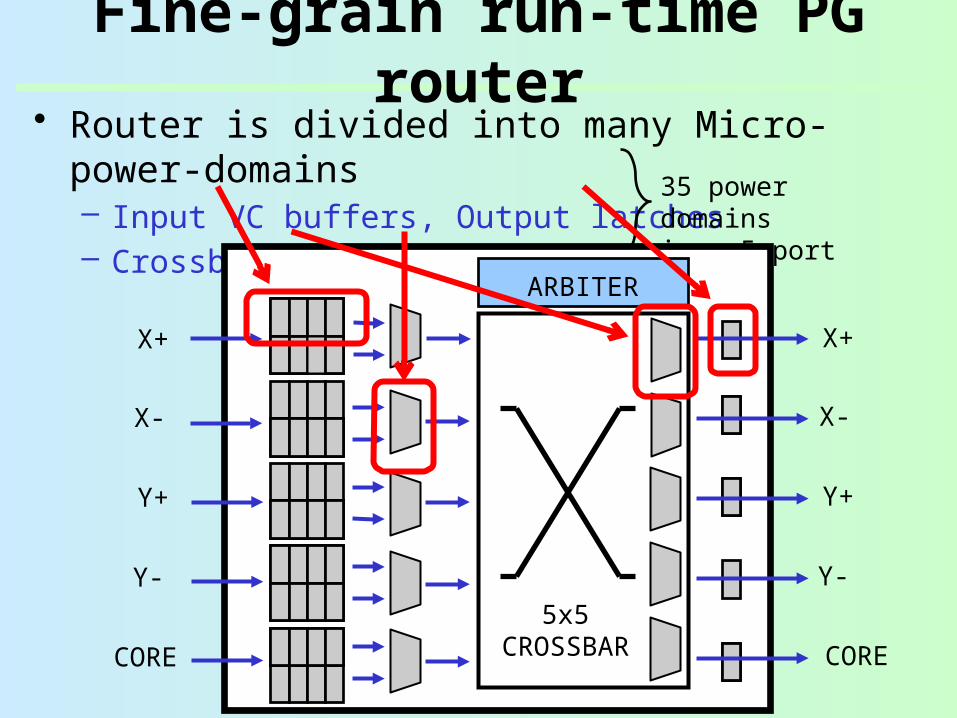
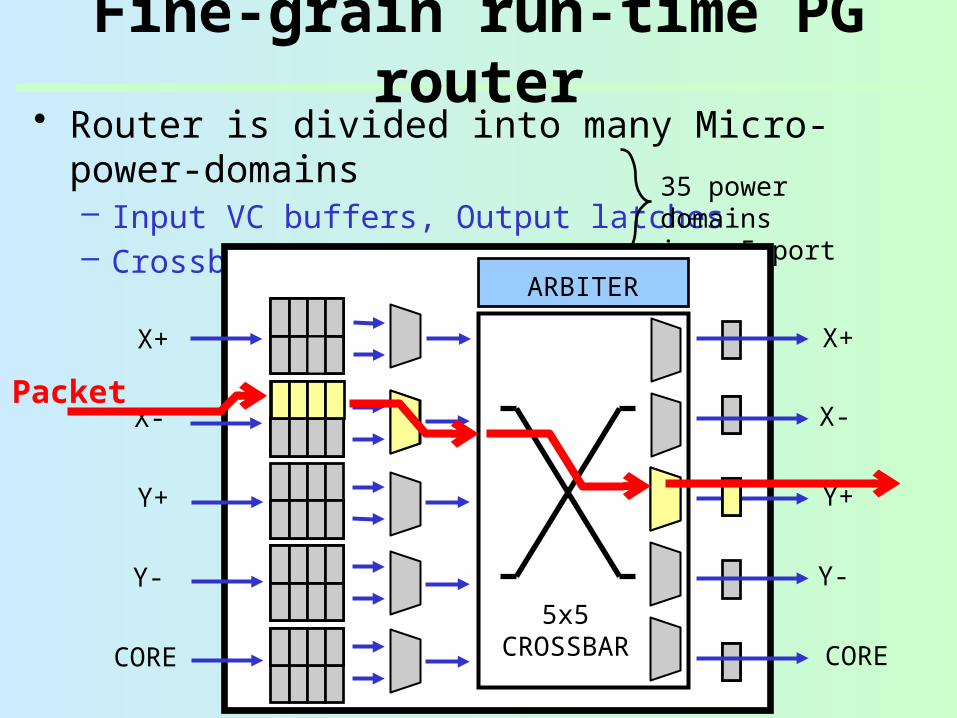
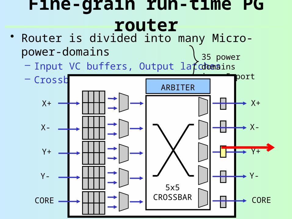
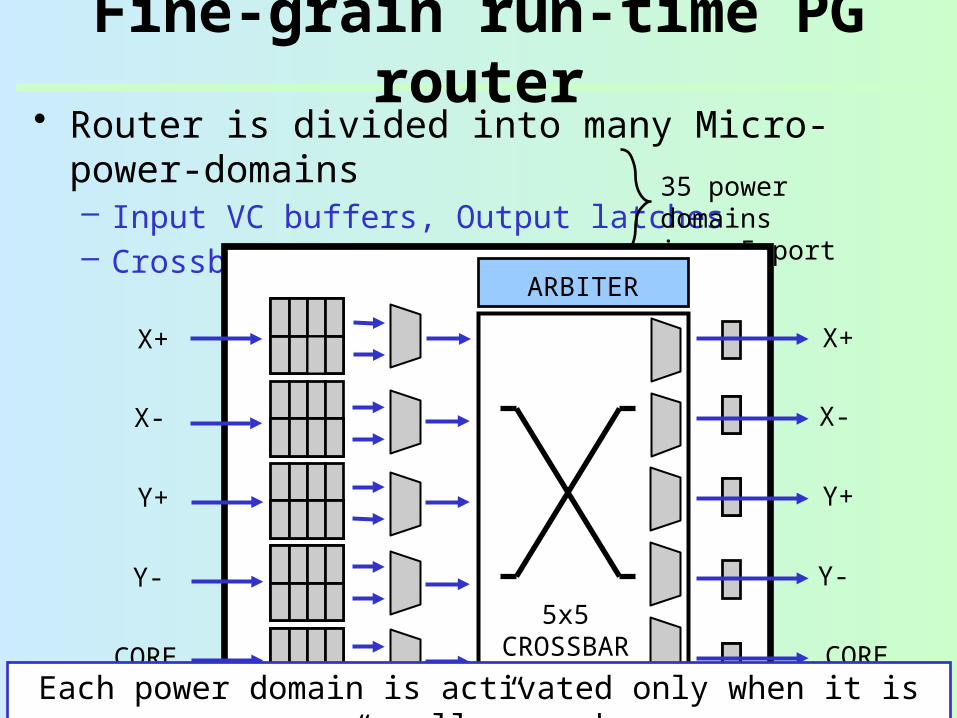
• Router is divided into many Micro-power-domains– Input VC buffers, Output latches– Crossbar MUXes, VC MUXes
Fine-grain run-time PG router
35 power domainsin a 5-port routerARBITER
X+
X-
Y+
Y-
CORE
X+
X-
Y+
Y-
CORE
5x5 CROSSBAR
• Router is divided into many Micro-power-domains– Input VC buffers, Output latches– Crossbar MUXes, VC MUXes
Fine-grain run-time PG router
35 power domainsin a 5-port routerARBITER
X+
X-
Y+
Y-
CORE
X+
X-
Y+
Y-
CORE
5x5 CROSSBAR
Packet

• Router is divided into many Micro-power-domains– Input VC buffers, Output latches– Crossbar MUXes, VC MUXes
Fine-grain run-time PG router
35 power domainsin a 5-port routerARBITER
X+
X-
Y+
Y-
CORE
X+
X-
Y+
Y-
CORE
5x5 CROSSBAR

• Router is divided into many Micro-power-domains– Input VC buffers, Output latches– Crossbar MUXes, VC MUXes
Fine-grain run-time PG router
35 power domainsin a 5-port routerARBITER
X+
X-
Y+
Y-
CORE
X+
X-
Y+
Y-
CORE
5x5 CROSSBAR
• Router is divided into many Micro-power-domains– Input VC buffers, Output latches– Crossbar MUXes, VC MUXes
Fine-grain run-time PG router
35 power domainsin a 5-port routerARBITER
X+
X-
Y+
Y-
CORE
X+
X-
Y+
Y-
CORE
5x5 CROSSBAR
• Router is divided into many Micro-power-domains– Input VC buffers, Output latches– Crossbar MUXes, VC MUXes
Fine-grain run-time PG router
35 power domainsin a 5-port routerARBITER
X+
X-
Y+
Y-
CORE
X+
X-
Y+
Y-
CORE
5x5 CROSSBAR
Each power domain is activated only when it is “really” used
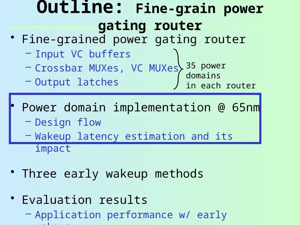
• Fine-grained power gating router– Input VC buffers– Crossbar MUXes, VC MUXes– Output latches
• Power domain implementation @ 65nm– Design flow– Wakeup latency estimation and its impact
• Three early wakeup methods
• Evaluation results– Application performance w/ early wakeup– Leakage power reduction
Outline: Fine-grain power gating router
35 power domainsin each router
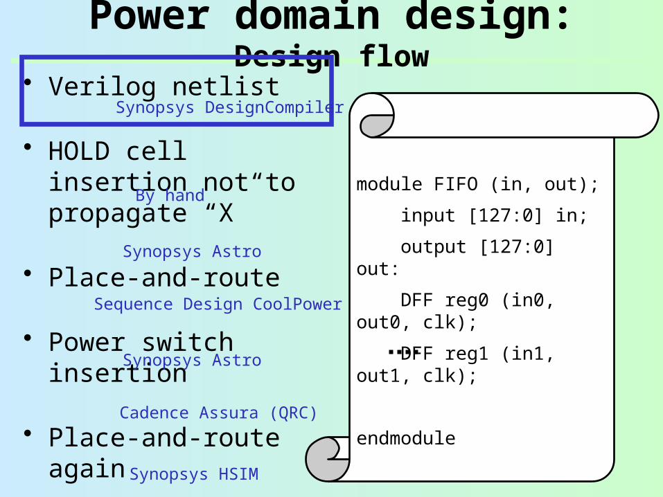
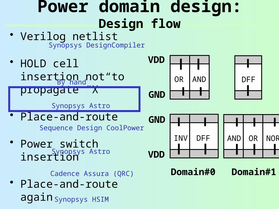
Power domain design: Design flow
• Verilog netlist
• HOLD cell insertion not to propagate “X”
• Place-and-route
• Power switch insertion
• Place-and-route again
• RC extraction
• SPICE simulation
module FIFO (in, out);
input [127:0] in;
output [127:0] out:
DFF reg0 (in0, out0, clk);
DFF reg1 (in1, out1, clk);
endmodule
Synopsys DesignCompiler
Synopsys Astro
Sequence Design CoolPower
Synopsys Astro
Cadence Assura (QRC)
Synopsys HSIM
By hand
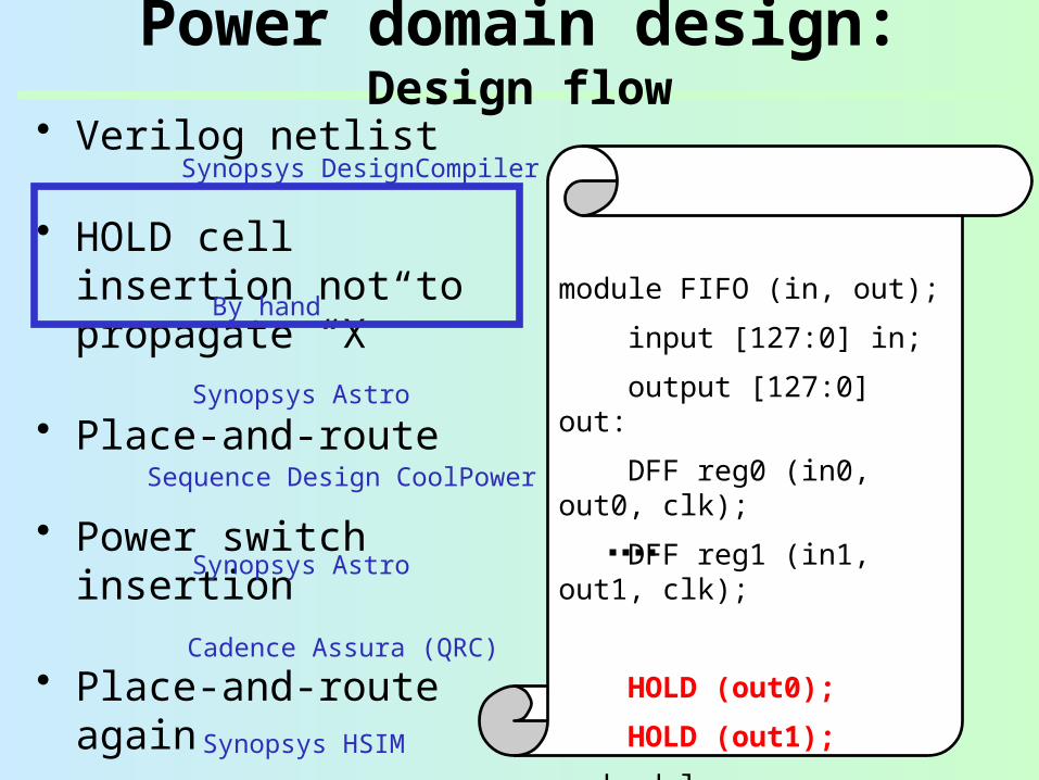
Power domain design: Design flow
• Verilog netlist
• HOLD cell insertion not to propagate “X”
• Place-and-route
• Power switch insertion
• Place-and-route again
• RC extraction
• SPICE simulation
module FIFO (in, out);
input [127:0] in;
output [127:0] out:
DFF reg0 (in0, out0, clk);
DFF reg1 (in1, out1, clk);
HOLD (out0);
HOLD (out1);
endmodule
Synopsys DesignCompiler
Synopsys Astro
Sequence Design CoolPower
Synopsys Astro
Cadence Assura (QRC)
Synopsys HSIM
By hand
Power domain design: Design flow
• Verilog netlist
• HOLD cell insertion not to propagate “X”
• Place-and-route
• Power switch insertion
• Place-and-route again
• RC extraction
• SPICE simulation
OR AND
VDD
GND
INV DFF
GND
VDD
AND OR NOR
DFF
Domain#0 Domain#1
Synopsys DesignCompiler
Synopsys Astro
Sequence Design CoolPower
Synopsys Astro
Cadence Assura (QRC)
Synopsys HSIM
By hand

Power domain design: Design flow
• Verilog netlist
• HOLD cell insertion not to propagate “X”
• Place-and-route
• Power switch insertion
• Place-and-route again
• RC extraction
• SPICE simulation
OR AND
VDD
GND
INV DFF
GND
VDD
VGND
AND OR NOR
DFF
PowerSwitch
Domain#0 Domain#1
Area overhead: Power switch and hold cells: 4.3% But, we need larger cells: 15.9% in total
Synopsys DesignCompiler
Synopsys Astro
Sequence Design CoolPower
Synopsys Astro
Cadence Assura (QRC)
Synopsys HSIM
By hand
Power domain design: Design flow
• Verilog netlist
• HOLD cell insertion not to propagate “X”
• Place-and-route
• Power switch insertion
• Place-and-route again
• RC extraction
• SPICE simulation
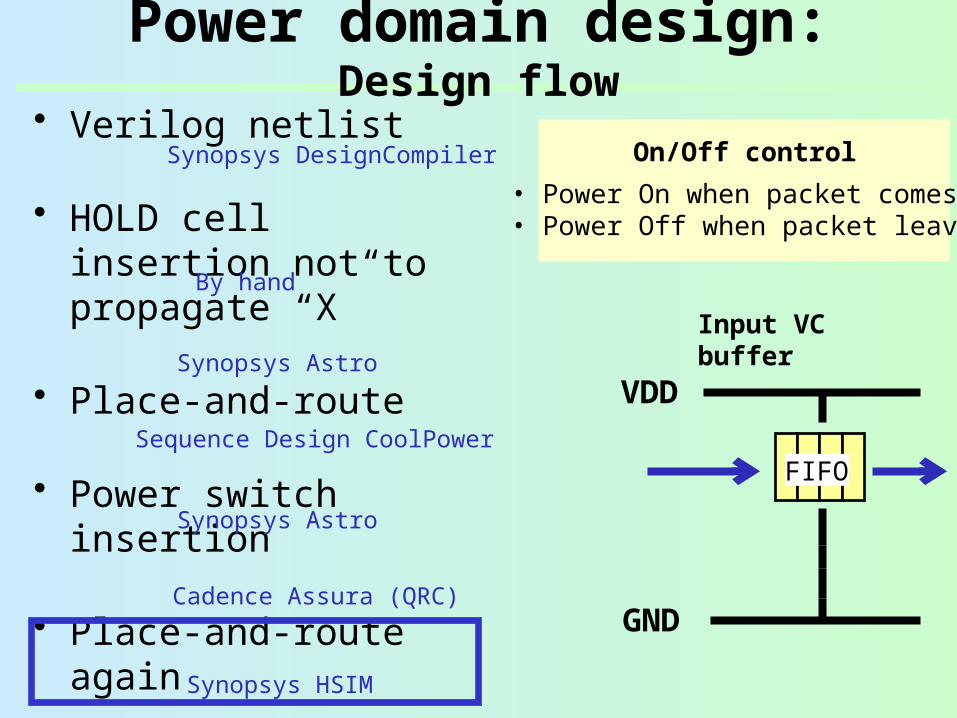
On/Off control
• Power On when packet comes• Power Off when packet leaves
VDD
GND
FIFO
Input VC buffer
Synopsys DesignCompiler
Synopsys Astro
Sequence Design CoolPower
Synopsys Astro
Cadence Assura (QRC)
Synopsys HSIM
By hand

Power domain design: Design flow
• Verilog netlist
• HOLD cell insertion not to propagate “X”
• Place-and-route
• Power switch insertion
• Place-and-route again
• RC extraction
• SPICE simulation
VDD
GND
FIFO
SwitchWakeup
VGND
FIFO
Input VC buffer
On/Off control
• Power On when packet comes• Power Off when packet leaves
Synopsys DesignCompiler
Synopsys Astro
Sequence Design CoolPower
Synopsys Astro
Cadence Assura (QRC)
Synopsys HSIM
By hand
Power domain design: Design flow
• Verilog netlist
• HOLD cell insertion not to propagate “X”
• Place-and-route
• Power switch insertion
• Place-and-route again
• RC extraction
• SPICE simulation
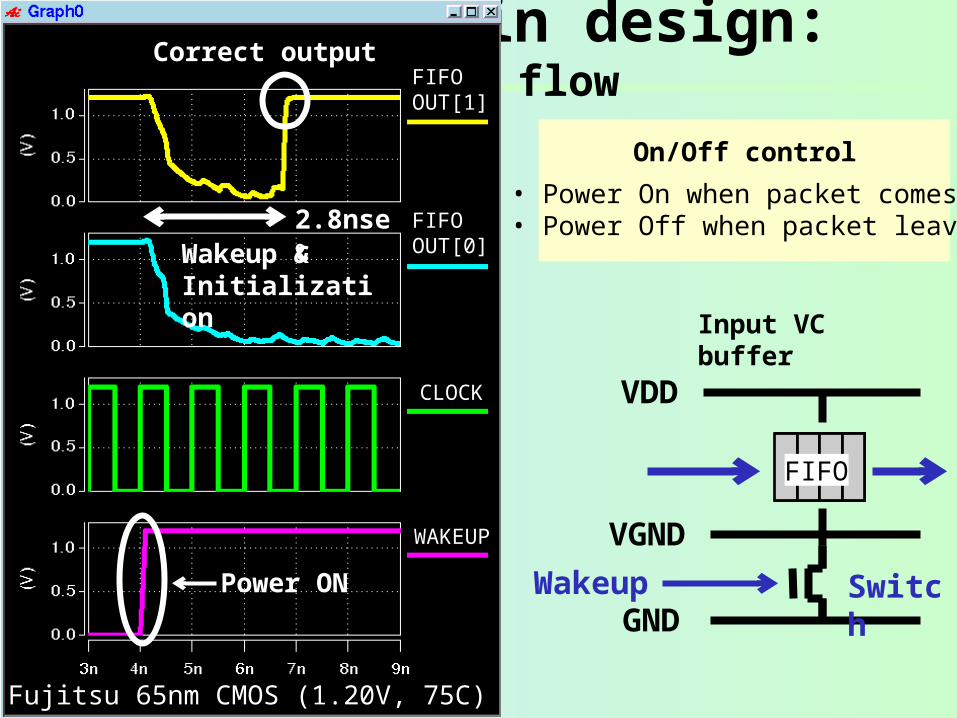
VDD
GND
FIFO
SwitchWakeup
VGND
FIFO
Power ON
WAKEUP
CLOCK
Correct output
Wakeup &Initialization
2.8nsec
FIFOOUT[0]
FIFOOUT[1]
Fujitsu 65nm CMOS (1.20V, 75C)
Input VC buffer
On/Off control
• Power On when packet comes• Power Off when packet leaves
Power domain design: Design flow
• Verilog netlist
• HOLD cell insertion not to propagate “X”
• Place-and-route
• Power switch insertion
• Place-and-route again
• RC extraction
• SPICE simulation
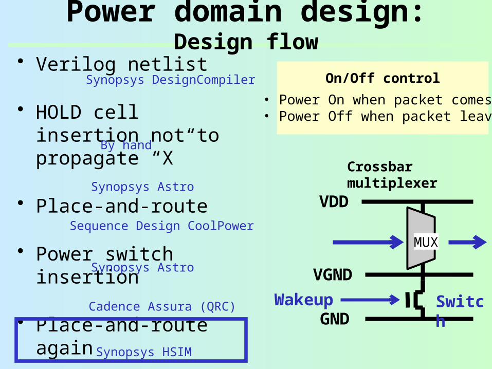
VDD
GNDSwitchWakeup
VGND
MUX
Crossbar multiplexer
MUX
On/Off control
• Power On when packet comes• Power Off when packet leaves
Synopsys DesignCompiler
Synopsys Astro
Sequence Design CoolPower
Synopsys Astro
Cadence Assura (QRC)
Synopsys HSIM
By hand
Power domain design: Design flow
• Verilog netlist
• HOLD cell insertion not to propagate “X”
• Place-and-route
• Power switch insertion
• Place-and-route again
• RC extraction
• SPICE simulation
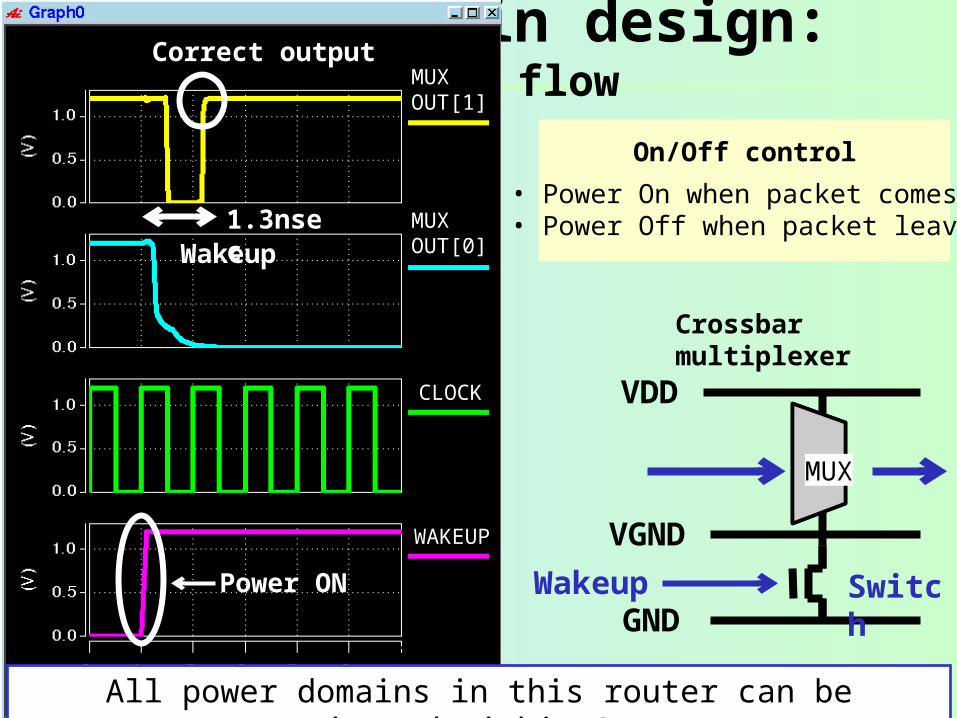
VDD
GNDSwitchWakeup
VGND
MUX
Crossbar multiplexer
MUX
Power ON
Wakeup
Correct output
CORE
Fujitsu 65nm CMOS (1.20V, 75C)
WAKEUP
MUXOUT[0]
MUXOUT[1]
CLOCK
1.3nsec
All power domains in this router can be activated within 3nsec
On/Off control
• Power On when packet comes• Power Off when packet leaves
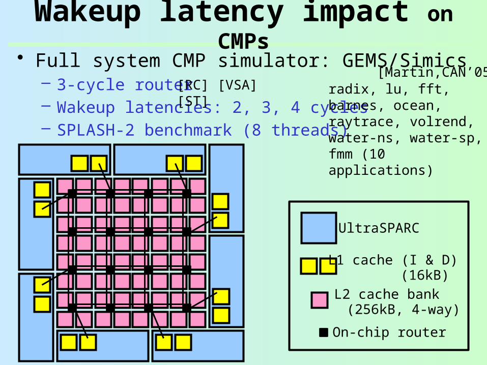
• Full system CMP simulator: GEMS/Simics– 3-cycle router– Wakeup latencies: 2, 3, 4 cycles– SPLASH-2 benchmark (8 threads)
Wakeup latency impact on CMPs
On-chip router
UltraSPARC
L1 cache (I & D)
L2 cache bank (16kB)
(256kB, 4-way)
[RC] [VSA] [ST] radix, lu, fft, barnes, ocean, raytrace, volrend, water-ns, water-sp, fmm (10 applications)
[Martin,CAN’05]
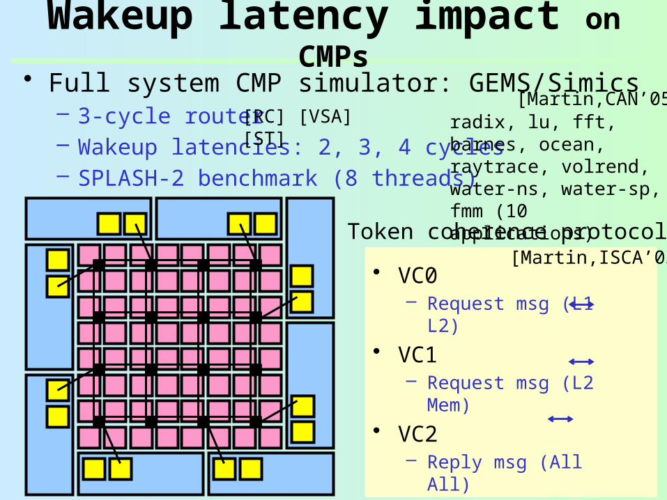
• Full system CMP simulator: GEMS/Simics– 3-cycle router– Wakeup latencies: 2, 3, 4 cycles– SPLASH-2 benchmark (8 threads)
Wakeup latency impact on CMPs
[RC] [VSA] [ST]
• VC0– Request msg (L1 L2)
• VC1– Request msg (L2
Mem)• VC2
– Reply msg (All All)• VC3
– Persistent request msg
radix, lu, fft, barnes, ocean, raytrace, volrend, water-ns, water-sp, fmm (10 applications)
Token coherence protocol[Martin,ISCA’03]
[Martin,CAN’05]

• Execution times of SPLASH-2 (10 applications) 3-cycle wait2-cycle wait 4-cycle wait
(@1000MHz)(@667MHz) (@1333MHz)
Execution time w/o power gating = 1.00
Wakeup latency impact: Results
Radix Lu Fft Barnes Ocean Ray-trace
Vol-rend
WaterNS
WaterSP
Fmm Ave
Execution time increases 23.2-46.3% (unacceptable!)
Longer execution consumes more power; Early wakeup required
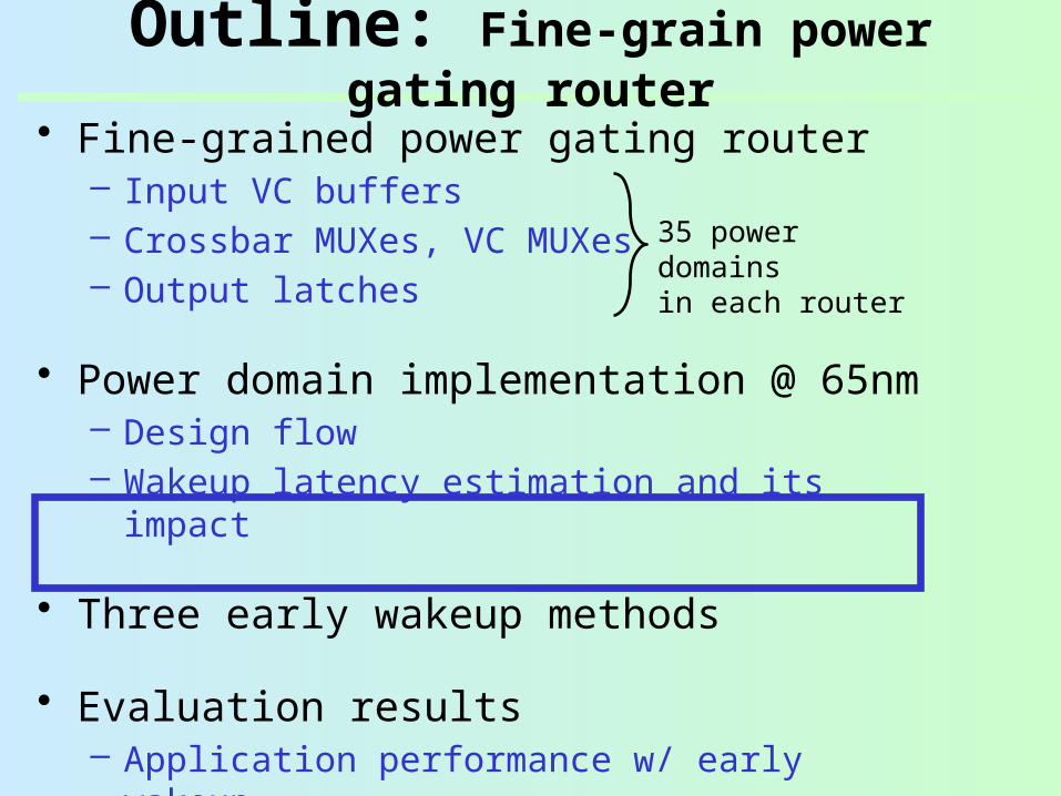
• Fine-grained power gating router– Input VC buffers– Crossbar MUXes, VC MUXes– Output latches
• Power domain implementation @ 65nm– Design flow– Wakeup latency estimation and its impact
• Three early wakeup methods
• Evaluation results– Application performance w/ early wakeup– Leakage power reduction
Outline: Fine-grain power gating router
35 power domainsin each router

• Router modules in 2-hop away activated in advance– Look-ahead routing is used– Wakeup procedure starts 4-cycle in advance
• Problems– Wakeup signals span 2-hop– Cannot wakeup the 1-hop router in advance
SRC DST
1-hop 2-hop 3-hop 4-hop
Wakeup Wakeup
[Matsutani, ASPDAC’08]
Suffers first-hop wakeup latency; Small benefit of look-ahead
(*) Average hop is 2.67 @ 4x4 mesh
Early wakeup: Look-ahead method

• Router modules in 2-hop away activated in advance– Look-ahead routing is used– Wakeup procedure starts 4-cycle in advance
• Ever-on domain– VC buffers connected from CPU are always active– No wait for the first-hop– But, they consume leakage
SRC DST
1-hop 2-hop 3-hop 4-hop
Wakeup Wakeup
+ CPU ever-on
Ever-on
Early wakeup: Look-ahead method
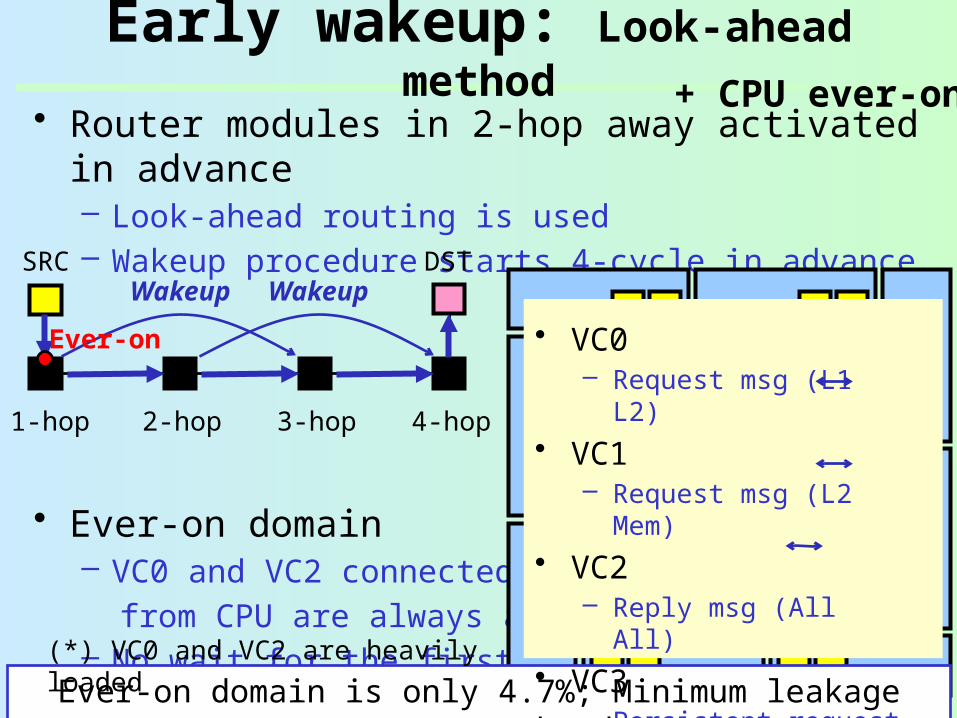
• Router modules in 2-hop away activated in advance– Look-ahead routing is used– Wakeup procedure starts 4-cycle in advance
• Ever-on domain– VC0 and VC2 connected from CPU are always active– No wait for the first-hop
SRC DST
1-hop 2-hop 3-hop 4-hop
Wakeup Wakeup
+ CPU ever-on
Ever-on
Ever-on domain is only 4.7%; Minimum leakage power overhead
Early wakeup: Look-ahead method
(*) VC0 and VC2 are heavily loaded
• VC0– Request msg (L1 L2)
• VC1– Request msg (L2
Mem)• VC2
– Reply msg (All All)• VC3
– Persistent request msg
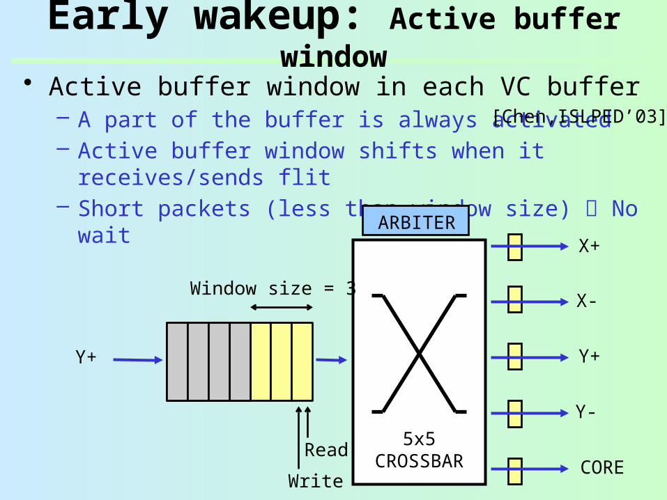
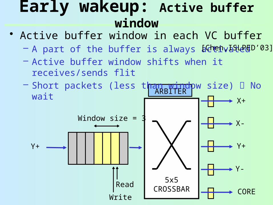
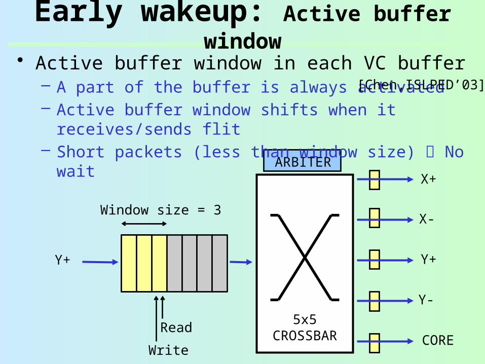
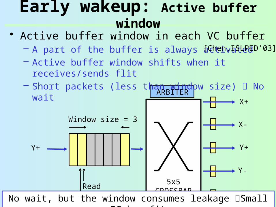
Early wakeup: Active buffer window
• Active buffer window in each VC buffer– A part of the buffer is always activated– Active buffer window shifts when it receives/sends
flit– Short packets (less than window size) No wait
5x5 CROSSBAR
ARBITER
Y+
X+
X-
Y+
Y-
CORERead
Write
Window size = 3
[Chen,ISLPED’03]
Early wakeup: Active buffer window
5x5 CROSSBAR
ARBITER
Y+
X+
X-
Y+
Y-
CORERead
Write
Window size = 3
• Active buffer window in each VC buffer– A part of the buffer is always activated– Active buffer window shifts when it receives/sends
flit– Short packets (less than window size) No wait
[Chen,ISLPED’03]
Early wakeup: Active buffer window
5x5 CROSSBAR
ARBITER
Y+
X+
X-
Y+
Y-
CORERead
Write
Window size = 3
No wait, but the window consumes leakage Small PG benefit
• Active buffer window in each VC buffer– A part of the buffer is always activated– Active buffer window shifts when it receives/sends
flit– Short packets (less than window size) No wait
[Chen,ISLPED’03]

• Fine-grained power gating router– Input VC buffers– Crossbar MUXes, VC MUXes– Output latches
• Power domain implementation @ 65nm– Design flow– Wakeup latency estimation and its impact
• Three early wakeup methods
• Evaluation results– Application performance w/ early wakeup– Leakage power reduction
Outline: Fine-grain power gating router
35 power domainsin each router
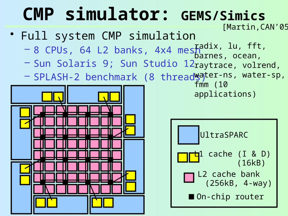
• Full system CMP simulation– 8 CPUs, 64 L2 banks, 4x4 mesh– Sun Solaris 9; Sun Studio 12– SPLASH-2 benchmark (8 threads)
On-chip router
UltraSPARC
L1 cache (I & D)
L2 cache bank (16kB)
(256kB, 4-way)
CMP simulator: GEMS/Simics
radix, lu, fft, barnes, ocean, raytrace, volrend, water-ns, water-sp, fmm (10 applications)
[Martin,CAN’05]

• Full system CMP simulation– 8 CPUs, 64 L2 banks, 4x4 mesh– Sun Solaris 9; Sun Studio 12– SPLASH-2 benchmark (8 threads)
CMP simulator: GEMS/Simics
radix, lu, fft, barnes, ocean, raytrace, volrend, water-ns, water-sp, fmm (10 applications)
Token coherence protocol
• VC0– Request msg (L1 L2)
• VC1– Request msg (L2
Mem)• VC2
– Reply msg (All All)• VC3
– Persistent request msg
[Martin,ISCA’03]
[Martin,CAN’05]
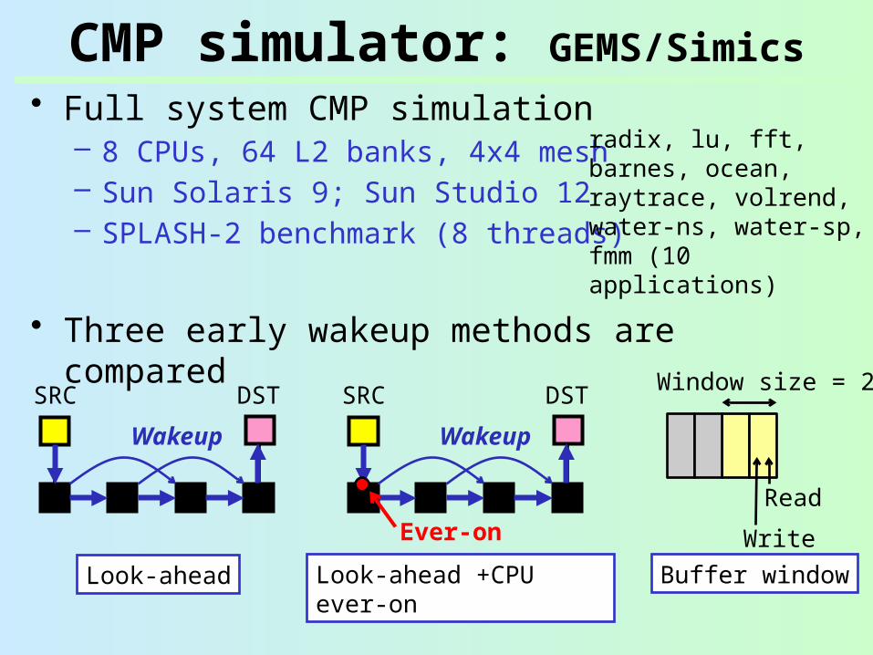
• Full system CMP simulation– 8 CPUs, 64 L2 banks, 4x4 mesh– Sun Solaris 9; Sun Studio 12– SPLASH-2 benchmark (8 threads)
• Three early wakeup methods are compared
• Wakeup latency: 3nsec (3-cycle wakeup @ 1GHz)
CMP simulator: GEMS/Simics
radix, lu, fft, barnes, ocean, raytrace, volrend, water-ns, water-sp, fmm (10 applications)
SRC DST
Wakeup
SRC DST
Wakeup
Read
Write
Window size = 2
Ever-on
Look-ahead Look-ahead +CPU ever-on
Buffer window

Execution time without early wakeup (+35.3%)
Performance overhead is only 4.0% (CPU-ever on)
Look-ahead withLook-ahead Buffer windowCPU ever-on
Execution times of SPLASH-2 (3-cycle wakeup @ 1GHz)
Evaluations: Application performance
Radix Lu Fft Barnes Ocean Ray-trace
Vol-rend
WaterNS
WaterSP
Fmm Ave
(1.00 = Execution time with no wakeup latency)
Early wakeup significantly mitigates the performance overhead

• Power gating is applied to the router with 3 steps
SRC DST
Wakeup
SRC DST
Wakeup
Read
Write
Window size = 2
Ever-on
Evaluations: Leakage power reduction
Look-ahead Look-ahead +CPU ever-on
Buffer window
Level-1 power gating Level-2 power gating Level-3 power gating
ARB ARB ARB
Input buffer + Xbar In/output buffer + XbarInput buffer only
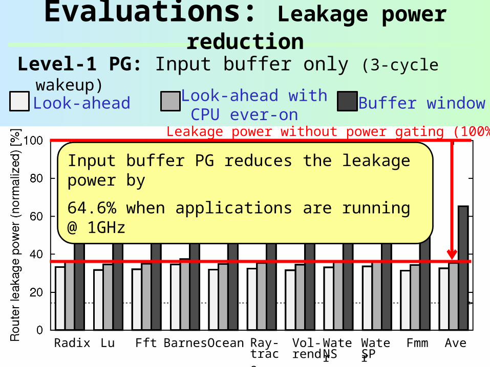
Level-1 PG: Input buffer only (3-cycle wakeup)
Leakage power without power gating (100%)
Input buffer PG reduces the leakage power by
64.6% when applications are running @ 1GHz
Look-ahead withLook-ahead Buffer windowCPU ever-on
Evaluations: Leakage power reduction
Radix Lu Fft Barnes Ocean Ray-trace
Vol-rend
WaterNS
WaterSP
Fmm Ave

Input buffer PG + Crossbar PG reduce the leakage power by 72.7% @ 1GHz
Leakage power without power gating (100%)
Look-ahead withLook-ahead Buffer windowCPU ever-on
Level-2 PG: Input buffer + Crossbar (3-cycle wakeup)
Evaluations: Leakage power reduction
Radix Lu Fft Barnes Ocean Ray-trace
Vol-rend
WaterNS
WaterSP
Fmm Ave

Input buffer PG + Crossbar PG + Output latch PG reduce the leakage power by 77.7% @ 1GHz
Leakage power without power gating (100%)
Look-ahead withLook-ahead Buffer windowCPU ever-on
Level-3 PG: Input buffer + Crossbar + Output latch
Evaluations: Leakage power reduction
Radix Lu Fft Barnes Ocean Ray-trace
Vol-rend
WaterNS
WaterSP
Fmm AveFine-grain PG with early wakeup reduces the leakage by
77.7%

• Power gating for router components– Input VC buffers– Crossbar MUXes, VC MUXes– Output latches– Wakeup latency is at most 3nsec
• Three early wakeup methods– Look-ahead– Look-ahead with CPU ever-on– Look-ahead with active buffer window
• Evaluation results– Performance overhead is less than 4.0% @
1GHz– Leakage power is reduced by 77.7%
Summary: Run-time PG router for CMPs
35 power domainsin each router

Thank you for your attention