ultra-compact photonic crystal waveguide spatial mode
TRANSCRIPT

Ultra-compact photonic crystalwaveguide spatial mode converter andits connection to the optical diode effect
Victor Liu,∗ David A. B. Miller, and Shanhui FanDepartment of Electrical Engineering, Stanford University, Stanford, California 94305 USA
Abstract: We design an extremely compact photonic crystal waveguidespatial mode converter which converts the fundamental even mode to thehigher order odd mode with nearly 100% efficiency. We adapt a previouslydeveloped design and optimization process that allows these types ofdevices to be designed in a matter of minutes. We also present an extremelycompact optical diode device and clarify its general properties and itsrelation to spatial mode converters. Finally, we connect the results here to ageneral theory on the complexity of optical designs.
© 2012 Optical Society of America
OCIS codes: (130.3120) Integrated optics devices; (130.2790) Guided waves; (230.3120) In-tegrated optics devices.
References and links1. J. Wang, J.-Y. Yang, I. M. Fazal, N. Ahmed, Y. Yan, H. Huang, Y. Ren, Y. Yue, S. Dolinar, M. Tur, and A. E.
Willner, “Terabit free-space data transmission employing orbital angular momentum multiplexing,” Nat. Photon.6, 488–496 (2012).
2. L. H. Gabrielli, D. Liu, S. G. Johnson, and M. Lipson, “On-chip transformation optics for multimode waveguidebends,” Nat. Commun. 3, 1217 (2012).
3. D. A. B. Miller, “All linear optical devices are mode converters,” Opt. Express 20, 23985–23993 (2012).4. D. A. B. Miller, “How complicated must an optical component be?,” Submitted to J. Opt. Soc. Am. A.
http://arxiv.org/abs/1209.5499.5. V. P. Tzolov and M. Fontaine, “A passive polarization converter free of longitudinally-periodic structure,” Opt.
Commun. 127, 7–13 (1996).6. T. D. Happ, M. Kamp, and A. Forchel, “Photonic crystal tapers for ultracompact mode conversion,” Opt. Lett.
26, 1102–1104 (2001).7. A. Talneau, P. Lalanne, M. Agio, and C. M. Soukoulis, “Low-reflection photonic-crystal taper for efficient cou-
pling between guide sections of arbitrary widths,” Opt. Lett. 27, 1522–1524 (2002).8. P. Sanchis, J. Marti, A. Garcia, A. Martinez, and J. Blasco, “High efficiency coupling technique for planar pho-
tonic crystal waveguides,” Electron. Lett. 38, 961–962 (2002).9. P. Lalanne and A. Talneau, “Modal conversion with artificial materials for photonic-crystal waveguides,” Opt.
Express 10, 354–359 (2002).10. P. Bienstman, S. Assefa, S. G. Johnson, J. D. Joannopoulos, G. S. Petrich, and L. A. Kolodziejski, “Taper struc-
tures for coupling into photonic crystal slab waveguides,” J. Opt. Soc. Am. B 20, 1817–1821 (2003).11. E. Khoo, A. Liu, and J. Wu, “Nonuniform photonic crystal taper for high-efficiency mode coupling,” Opt. Express
13, 7748–7759 (2005).12. J. Castro, D. F. Geraghty, S. Honkanen, C. M. Greiner, D. Iazikov, and T. W. Mossberg, “Demonstration of mode
conversion using anti-symmetric waveguide bragg gratings,” Opt. Express 13, 4180–4184 (2005).13. S. Y. Tseng and M. C. Wu, “Adiabatic mode conversion in multimode waveguides using computer-generated
planar holograms,” IEEE Photon. Technol. Lett. 22, 1211–1213 (2010).14. P. Sanchis, J. Marti, J. Blasco, A. Martinez, and A. Garcia, “Mode matching technique for highly efficient cou-
pling between dielectric waveguides and planar photonic crystal circuits,” Opt. Express 10, 1391–1397 (2002).15. I. L. Gheorma, S. Haas, and A. F. J. Levi, “Aperiodic nanophotonic design,” J. Appl. Phys. 95, 1420–1426 (2004).
#178467 - $15.00 USD Received 22 Oct 2012; revised 19 Nov 2012; accepted 23 Nov 2012; published 6 Dec 2012(C) 2012 OSA 17 December 2012 / Vol. 20, No. 27 / OPTICS EXPRESS 28388

16. Y. Jiao, S. Fan, and D. A. B. Miller, “Demonstration of systematic photonic crystal device design and optimizationby low-rank adjustments: an extremely compact mode separator,” Opt. Lett. 30, 141–143 (2005).
17. V. Liu, Y. Jiao, D. A. B. Miller, and S. Fan, “Design methodology for compact photonic-crystal-based wavelengthdivision multiplexers,” Opt. Lett. 36, 591–593 (2011).
18. G. G. Denisov, G. I. Kalynova, and D. I. Sobolev, “Method for synthesis of waveguide mode converters,” Radio-phys. Quantum El. 47, 615–620 (2004).
19. M. Qiu, “Effective index method for heterostructure-slab-waveguide-based two-dimensional photonic crystals,”Appl. Phys. Lett. 81, 1163–1165 (2002).
20. Y. Li and J.-M. Jin, “A vector dual-primal finite element tearing and interconnecting method for solving 3-Dlarge-scale electromagnetic problems,” IEEE Trans. Antennas Propag. 54, 3000–3009 (2006).
21. G. Veronis, R. W. Dutton, and S. Fan, “Method for sensitivity analysis of photonic crystal devices,” Opt. Lett.29, 2288–2290 (2004).
22. Y. Jiao, S. Fan, and D. A. B. Miller, “Systematic photonic crystal device design: global and local optimizationand sensitivity analysis,” IEEE J. Quantum Elect. 42, 266–279 (2006).
23. V. Liu, D. A. B. Miller, and S. Fan, “Highly tailored computational electromagnetics methods for nanophotonicdesign and discovery,” Proc. IEEE (Accepted).
24. Y. Huang and Y. Y. Lu, “Scattering from periodic arrays of cylinders by dirichlet-to-neumann maps,” J. LightwaveTechnol. 24, 3448–3453 (2006).
25. Z. Hu and Y. Y. Lu, “Efficient analysis of photonic crystal devices by dirichlet-to-neumann maps,” Opt. Express16, 17383–17399 (2008).
26. M. Greenberg and M. Orenstein, “Irreversible coupling by use of dissipative optics,” Opt. Lett. 29, 451–453(2004).
27. L. Feng, M. Ayache, J. Huang, Y.-L. Xu, M.-H. Lu, Y.-F. Chen, Y. Fainman, and A. Scherer, “Nonreciprocal lightpropagation in a silicon photonic circuit,” Science 333, 729–733 (2011).
28. A. E. Serebryannikov, “One-way diffraction effects in photonic crystal gratings made of isotropic materials,”Phys. Rev. B 80, 155117 (2009).
29. C. Wang, C.-Z. Zhou, and Z.-Y. Li, “On-chip optical diode based on silicon photonic crystal heterojunctions,”Opt. Express 19, 26948–26955 (2011).
30. C. Lu, X. Hu, H. Yang, and Q. Gong, “Ultrahigh-contrast and wideband nanoscale photonic crystal all-opticaldiode,” Opt. Lett. 36, 4668–4670 (2011).
31. S. Fan, R. Baets, A. Petrov, Z. Yu, J. D. Joannopoulos, W. Freude, A. Melloni, M. Popovic, M. Vanwolleghem,D. Jalas, M. Eich, M. Krause, H. Renner, E. Brinkmeyer, and C. R. Doerr, Comment on “nonreciprocal lightpropagation in a silicon photonic circuit,” Science 335, 38 (2012).
1. Introduction
There is growing interest using multiple spatial modes in optical systems to increase infor-mation processing capacity [1]. Much of the existing work has been focused on fiber opticcommunications, but there is also interest in developing integrated on-chip applications [2].The basic building blocks of these systems are components that can perform spatial mode ma-nipulation with minimal crosstalk over a wide bandwidth. Also, from a more fundamental pointof view, spatial mode manipulation has provided a model to understand complexities in opticaldevices in general [3, 4].
One important class of devices is those that convert one waveguide mode into another. Asidefrom applications which require their explicit functionality, mode converters are necessary toexcite higher order waveguide modes due to the difficulty in coupling modes other than thefundamental into a waveguide from free space. This conversion is conventionally performedadiabatically using tapered waveguide designs that are tens or hundreds of wavelengths long [5–13]. More compact designs have also been shown with good, though still limited, conversionefficiency [14].
We present here an extremely compact photonic crystal waveguide mode converter whichconverts the fundamental even-symmetric waveguide mode into the second order odd-symmetric mode, and vice versa, in a length of four wavelengths, with nearly 100% conversionefficiency. We also show a smaller structure which performs mode conversion of only one modeand we discuss its relationship to the optical diode effect.
We employ an aperiodic design methodology [15–17] that does not assume the adiabatic
#178467 - $15.00 USD Received 22 Oct 2012; revised 19 Nov 2012; accepted 23 Nov 2012; published 6 Dec 2012(C) 2012 OSA 17 December 2012 / Vol. 20, No. 27 / OPTICS EXPRESS 28389

coupling that is typical of existing design approaches [18]. The ability to efficiently designnon-trivial compact devices for mode manipulation enables the design of integrated photonicsystems which make use of higher order waveguide modes. Although the presented designsare idealized 2D structures, there have been recent efforts to implement such designs usingeffective index models in 3D for planar fabrication [19]. Full field numerical simulations alsoverify the functionality of 3D structures based on planar 2D designs [20].
Fig. 1. Schematic of template structure. Background dielectric rods are indicated with solidcircles. Black open circles are the 20 rods that can be added or removed, while the blackdashed circles are determined automatically by inversion symmetry. The blue highlightedregions show the waveguides, and the orange highlighted region shows the coupler regionwhere search and optimization are performed.
2. Mode converter
2.1. Design considerations based on general properties of the scattering matrix
The structures we consider are modifications of a background photonic crystal of silicon rods(ε = 12) of radius 0.2a in air (ε = 1) on a square lattice of lattice constant a (Fig. 1). Thefields are polarized with the electric field out-of-plane. The input and output waveguides (blueregions in Fig. 1) are formed by removing two lines of rods. These waveguides support twomodes: a fundamental even-symmetric mode and a higher order odd-symmetric mode. Our aimis to design the coupler region (orange region in Fig. 1) between the waveguides that enablesmodal conversion.
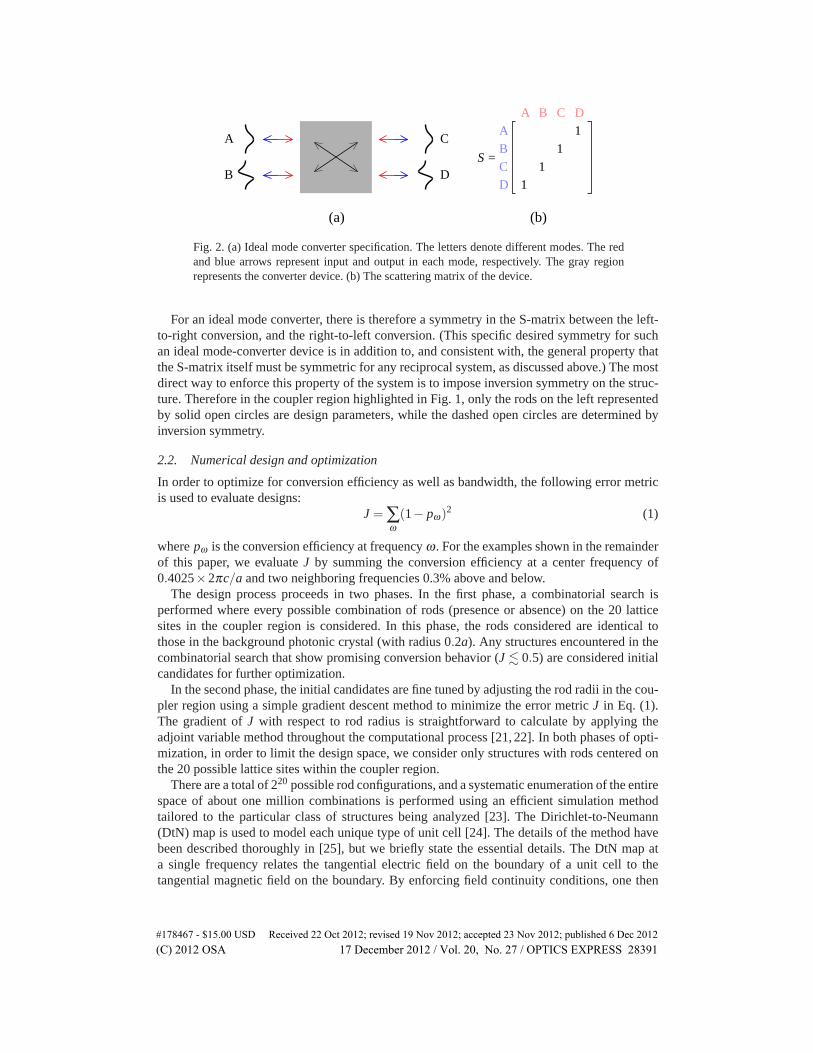
An ideal mode-converter device completely converts the fundamental even mode to thehigher order odd mode, and completely converts the odd mode to the even mode, as illus-trated symbolically with its corresponding scattering matrix in Fig. 2. We will denote by theletters A and B the even and odd modes, respectively, to the left of the coupler. Similarly, theletters C and D will denote the even and odd modes, respectively, to the right of the coupler.The scattering matrix relates the amplitudes of the out-going A, B, C, and D modes (indicatedin blue in Fig. 2) to the amplitudes of the in-going A, B, C, and D modes (indicated in red inFig. 2). Note that the phases of the modes can always be defined to make the scattering matrixhave the given form with purely real entries.
Any reciprocal structure that enables 100% transmission of an incident even mode on theleft to the odd mode on the right must necessarily provide complete transmission as well foran incident odd mode on the right to the even mode on the left. Such reciprocity holds for anypassive and linear structure consisting only of materials described by scalar permittivity andpermeability, as is the case here. Analogously, complete transmission of an incident odd modeon the left to the even mode on the right necessarily implies complete transmission of an evenmode from the right to the odd mode on the left. Since an ideal mode converter performs bothof these conversions, it must have identical behavior in both directions.
#178467 - $15.00 USD Received 22 Oct 2012; revised 19 Nov 2012; accepted 23 Nov 2012; published 6 Dec 2012(C) 2012 OSA 17 December 2012 / Vol. 20, No. 27 / OPTICS EXPRESS 28390
11
11
DCBA
A B C D
S =
A
B
C
D
(a) (b)
Fig. 2. (a) Ideal mode converter specification. The letters denote different modes. The redand blue arrows represent input and output in each mode, respectively. The gray regionrepresents the converter device. (b) The scattering matrix of the device.
For an ideal mode converter, there is therefore a symmetry in the S-matrix between the left-to-right conversion, and the right-to-left conversion. (This specific desired symmetry for suchan ideal mode-converter device is in addition to, and consistent with, the general property thatthe S-matrix itself must be symmetric for any reciprocal system, as discussed above.) The mostdirect way to enforce this property of the system is to impose inversion symmetry on the struc-ture. Therefore in the coupler region highlighted in Fig. 1, only the rods on the left representedby solid open circles are design parameters, while the dashed open circles are determined byinversion symmetry.
2.2. Numerical design and optimization
In order to optimize for conversion efficiency as well as bandwidth, the following error metricis used to evaluate designs:
J = ∑ω(1− pω)
2 (1)
where pω is the conversion efficiency at frequency ω . For the examples shown in the remainderof this paper, we evaluate J by summing the conversion efficiency at a center frequency of0.4025×2πc/a and two neighboring frequencies 0.3% above and below.
The design process proceeds in two phases. In the first phase, a combinatorial search isperformed where every possible combination of rods (presence or absence) on the 20 latticesites in the coupler region is considered. In this phase, the rods considered are identical tothose in the background photonic crystal (with radius 0.2a). Any structures encountered in thecombinatorial search that show promising conversion behavior (J � 0.5) are considered initialcandidates for further optimization.
In the second phase, the initial candidates are fine tuned by adjusting the rod radii in the cou-pler region using a simple gradient descent method to minimize the error metric J in Eq. (1).The gradient of J with respect to rod radius is straightforward to calculate by applying theadjoint variable method throughout the computational process [21, 22]. In both phases of opti-mization, in order to limit the design space, we consider only structures with rods centered onthe 20 possible lattice sites within the coupler region.
There are a total of 220 possible rod configurations, and a systematic enumeration of the entirespace of about one million combinations is performed using an efficient simulation methodtailored to the particular class of structures being analyzed [23]. The Dirichlet-to-Neumann(DtN) map is used to model each unique type of unit cell [24]. The details of the method havebeen described thoroughly in [25], but we briefly state the essential details. The DtN map ata single frequency relates the tangential electric field on the boundary of a unit cell to thetangential magnetic field on the boundary. By enforcing field continuity conditions, one then
#178467 - $15.00 USD Received 22 Oct 2012; revised 19 Nov 2012; accepted 23 Nov 2012; published 6 Dec 2012(C) 2012 OSA 17 December 2012 / Vol. 20, No. 27 / OPTICS EXPRESS 28391

obtains a linear system Ax = b where x represents the fields on the boundaries of the unit cells,b represents the incident wave source, and A is the system matrix formed from the DtN maps.
In the initial combinatorial search, only two unit cell types are present, so only two differ-ent DtN maps need to be computed. For the special case of rods in air, the DtN map can becomputed with cylindrical wave expansions, and this basis is sufficiently accurate that only 5unknowns per unit cell edge are required (verification with 7 unknowns per edge yields es-sentially identical results). Therefore, for the structures shown, the resulting linear system hasdimensions 8652. On a local cluster with 80 cores, the entire combinatorial search of 220 struc-tures at a single frequency can be completed in 10 minutes, while the subsequent gradientoptimization usually takes no longer than 5 minutes on a personal computer.
2.3. Results
One configuration which achieved very high conversion efficiency is shown in Fig. 3. All therods in this structure are identical (r = 0.2a), and further optimization of rod radius did not pro-duce substantial improvement in device performance. As shown in Fig. 3(a), the mode converterexhibits greater than 99% peak conversion efficiency from mode A to mode D with a relativefrequency width of 0.176% at the 90% threshold. For a center wavelength at 1.55 μm, thiscorresponds to a bandwidth of 2.73 nm. Note that the spectrum for the other three conversionprocesses (B to C, C to B, D to A) must all have the same spectrum, as required by inversionsymmetry and reciprocity. Therefore when considering the scattering matrix of this device, onecan immediately see that it performs as a nearly perfect mode converter. Quantitatively, thereflection (from a mode back into the same mode) and crosstalk (conversion efficiency to anunwanted mode) parameters at the operating frequency of ω = 0.4025× 2πc/a are all lowerthan −45 dB, demonstrating excellent suppression of undesired behavior. Representative fieldpatterns for the device for the A to D conversion and the B to C conversion are shown inFig. 3(b). The entire coupler region occupies an area of 4× 10 unit cells, which is about fourwavelengths long and two wavelengths wide. To the best of our knowledge, this is the mostcompact design of a dielectric mode converter at the present time.
(a) (b)
0
0.2
0.4
0.6
0.8
1
0.39 0.4 0.41
Con
vers
ion
effic
ienc
y
Normalized frequency (2πc/a)
A → D
Fig. 3. (a) Spectral conversion efficiency of the mode converter shown in the right side ofFig. 1. (b) Representative field patterns for both input modes from the left at normalizedfrequency 0.4025×2πc/a.
#178467 - $15.00 USD Received 22 Oct 2012; revised 19 Nov 2012; accepted 23 Nov 2012; published 6 Dec 2012(C) 2012 OSA 17 December 2012 / Vol. 20, No. 27 / OPTICS EXPRESS 28392
11
11
DCBA
A B C D
S =
A
B
C
D
(a) (b)
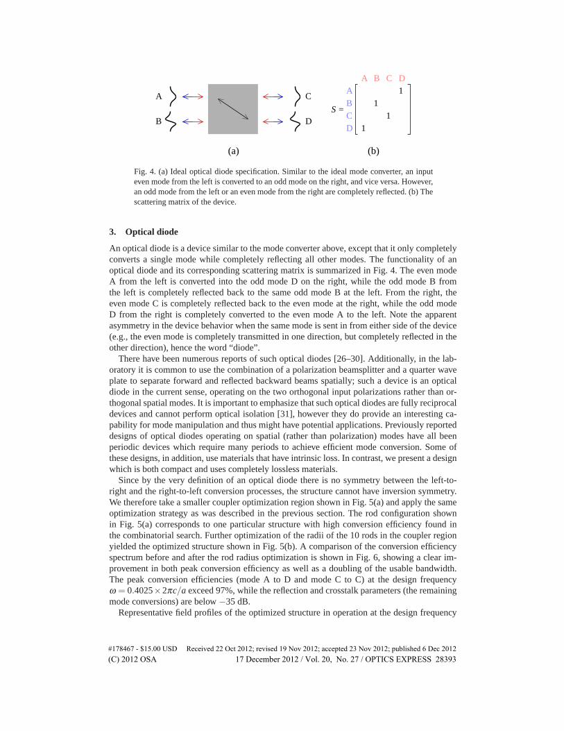
Fig. 4. (a) Ideal optical diode specification. Similar to the ideal mode converter, an inputeven mode from the left is converted to an odd mode on the right, and vice versa. However,an odd mode from the left or an even mode from the right are completely reflected. (b) Thescattering matrix of the device.
3. Optical diode
An optical diode is a device similar to the mode converter above, except that it only completelyconverts a single mode while completely reflecting all other modes. The functionality of anoptical diode and its corresponding scattering matrix is summarized in Fig. 4. The even modeA from the left is converted into the odd mode D on the right, while the odd mode B fromthe left is completely reflected back to the same odd mode B at the left. From the right, theeven mode C is completely reflected back to the even mode at the right, while the odd modeD from the right is completely converted to the even mode A to the left. Note the apparentasymmetry in the device behavior when the same mode is sent in from either side of the device(e.g., the even mode is completely transmitted in one direction, but completely reflected in theother direction), hence the word “diode”.
There have been numerous reports of such optical diodes [26–30]. Additionally, in the lab-oratory it is common to use the combination of a polarization beamsplitter and a quarter waveplate to separate forward and reflected backward beams spatially; such a device is an opticaldiode in the current sense, operating on the two orthogonal input polarizations rather than or-thogonal spatial modes. It is important to emphasize that such optical diodes are fully reciprocaldevices and cannot perform optical isolation [31], however they do provide an interesting ca-pability for mode manipulation and thus might have potential applications. Previously reporteddesigns of optical diodes operating on spatial (rather than polarization) modes have all beenperiodic devices which require many periods to achieve efficient mode conversion. Some ofthese designs, in addition, use materials that have intrinsic loss. In contrast, we present a designwhich is both compact and uses completely lossless materials.
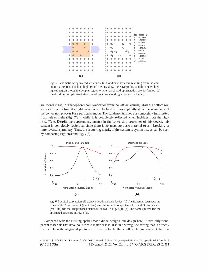
Since by the very definition of an optical diode there is no symmetry between the left-to-right and the right-to-left conversion processes, the structure cannot have inversion symmetry.We therefore take a smaller coupler optimization region shown in Fig. 5(a) and apply the sameoptimization strategy as was described in the previous section. The rod configuration shownin Fig. 5(a) corresponds to one particular structure with high conversion efficiency found inthe combinatorial search. Further optimization of the radii of the 10 rods in the coupler regionyielded the optimized structure shown in Fig. 5(b). A comparison of the conversion efficiencyspectrum before and after the rod radius optimization is shown in Fig. 6, showing a clear im-provement in both peak conversion efficiency as well as a doubling of the usable bandwidth.The peak conversion efficiencies (mode A to D and mode C to C) at the design frequencyω = 0.4025×2πc/a exceed 97%, while the reflection and crosstalk parameters (the remainingmode conversions) are below −35 dB.
Representative field profiles of the optimized structure in operation at the design frequency
#178467 - $15.00 USD Received 22 Oct 2012; revised 19 Nov 2012; accepted 23 Nov 2012; published 6 Dec 2012(C) 2012 OSA 17 December 2012 / Vol. 20, No. 27 / OPTICS EXPRESS 28393
1
2
3
4
5
6
7
8
9
10
Rod Radius (a)1 0.2038902 0.2182173 0.2348644 0.2280315 0.1514586 0.1094027 0.1151918 0.1013499 0.22417110 0.226149
(a) (b)
Fig. 5. Schematic of optimized structures. (a) Candidate structure resulting from the com-binatorial search. The blue highlighted regions show the waveguides, and the orange high-lighted region shows the coupler region where search and optimization are performed. (b)Final rod radius optimized structure of the corresponding structure on the left.
are shown in Fig. 7. The top row shows excitation from the left waveguide, while the bottom rowshows excitation from the right waveguide. The field profiles explicitly show the asymmetry ofthe conversion process for a particular mode. The fundamental mode is completely transmittedfrom left to right (Fig. 7(a)), while it is completely reflected when incident from the right(Fig. 7(c)). Despite the apparent asymmetry in the conversion properties of this device, thissystem is completely reciprocal since there is no magneto-optic material or any breaking oftime-reversal symmetry. Thus, the scattering matrix of the system is symmetric, as can be seenby comparing Fig. 7(a) and Fig. 7(d).
(a) (b)
0
0.2
0.4
0.6
0.8
1
0.39 0.4 0.41
Con
vers
ion
effic
ienc
y
Normalized frequency (2πc/a)
Initial search candidate
A → DC → C
0
0.2
0.4
0.6
0.8
1
0.39 0.4 0.41
Normalized frequency (2πc/a)
Optimized structure
A → DC → C
Fig. 6. Spectral conversion efficiency of optical diode device. (a) The transmission spectrumfrom mode A to mode D (black line) and the reflection spectrum for mode C to mode C(red line) for the unoptimized structure shown in Fig. 5(a). (b) The same spectra for theoptimized structure in Fig. 5(b).
Compared with the existing spatial mode diode designs, our design here utilizes only trans-parent materials that have no intrinsic material loss. It is in a waveguide setting that is directlycompatible with integrated photonics. It has probably the smallest design footprint that has
#178467 - $15.00 USD Received 22 Oct 2012; revised 19 Nov 2012; accepted 23 Nov 2012; published 6 Dec 2012(C) 2012 OSA 17 December 2012 / Vol. 20, No. 27 / OPTICS EXPRESS 28394

Fig. 7. Field patterns of the radius-optimized optical diode device shown in Fig. 5(b). Thetop row shows excitation from the left, while the bottom row shows excitation from theright.
ever been reported, and has near ideal performance as far as the apparent contrast in the twodirections is concerned.
It is important to emphasize that the structures presented above are not isolated instances ofstructures exhibiting high conversion efficiency. For example, in the combinatorial search forthe optical diode, more than 10 such structures were found, with spectra shown in Fig. 8. There-fore, our design method, when given a sufficiently large search space, is capable of producingmany possible designs which might be required if additional design constraints are imposed.
4. Design complexity
The numerical design here is directly connected to a general theory on the design complexity ofoptical devices. We can consider the complexity required in our designs by using the approachof Ref. [4]. In general, it is not possible to state the complexity required for any one devicedesign [4]; we can, however, state the complexity required to choose any one of a family ofdevices [4]. In the terminology of [4], at least at one specific frequency, the devices in Figs. 1,2, 4, and 5 have potentially 4 input modes (MI = 4) and 4 output modes (MO = 4). The mostgeneral linear device relating input to output modes could therefore be represented by a 4× 4device matrix, which in this case is the same matrix as the most general 4×4 scattering matrix.That most general device matrix would require therefore 16 complex numbers, correspondingto 32 real numbers (a “complexity number” ND = 32 [4]) that might have to be specified some-where in the device design. The devices we design here are presumed to be lossless (and hencerepresented by a unitary matrix) and reciprocal, and we likely do not care about the phase ofthe output beams relative to the input beams. We can follow the counting approaches in [4] toestablish the complexity number required for an arbitrary device that also satisfies these vari-ous constraints and flexibilities. If we wanted to have the freedom to design specific responsesfor more than one frequency, then in the worst case we would have to multiply the number of
#178467 - $15.00 USD Received 22 Oct 2012; revised 19 Nov 2012; accepted 23 Nov 2012; published 6 Dec 2012(C) 2012 OSA 17 December 2012 / Vol. 20, No. 27 / OPTICS EXPRESS 28395

0
0.2
0.4
0.6
0.8
1
0.39 0.4 0.41
Con
vers
ion
effic
ienc
y
Normalized frequency (2πc/a)
Fig. 8. Final candidate spectra obtained from the combinatorial search over 220 possibilitiesat frequencies near 0.4× 2πc/a. The vertical axis shows the conversion efficiency frommode A to mode D, and only spectra for structures with peak efficiency greater than 95%are shown.
spatial input and output modes by the number of frequencies, though we will not consider thisfurther here. See Ref. [4] for a discussion of design complexity with multiple frequencies.
First, since the device is to be unitary, the device matrix is necessarily square (unitary trans-formations retain orthogonality, which requires the corresponding matrices are square, for ex-ample). For an M×M unitary matrix, to specify the first column of the matrix requires 2M−1real numbers (the “−1” arises because the sum of the modulus squared elements must equal1, thus reducing the real degrees of freedom by 1 in the choice of these numbers). In general,for the second column of a unitary matrix, it must be orthogonal to the first column, whichmeans both the real and imaginary parts of the inner product of these two columns must bezero, thereby reducing the number of degrees of freedom by 2, so that second column can onlyhave 2M − 3 real degrees of freedom to specify it. Additionally, because the matrix here is tobe symmetric, the top element of this column must be the same as the second row elementof the first column, reducing the degrees of freedom by a further 2, leaving 2M − 5. For eachsuccessive column, if required, we reduce the degrees of freedom by a further 4. We only needto continue until we have specified half the columns (i.e., M/2); the other columns are thenall known as a result of the matrix symmetry and the orthogonality of the columns. The to-tal number of degrees of freedom (real numbers) to specify this unitary symmetric matrix istherefore
(2M−1)+(2M−5)+ · · ·+[2M−4
(M2−1
)−1
]=
M2(M+1) (2)
Since we do not care about the phase of the outputs relative to the inputs, we have one less realconstraint for each of the M/2 columns we can specify, so the final complexity number for anarbitrary unitary symmetric operator with floating output phases is
ND = M2/2 (3)
For our present devices, with M = 4, we therefore have ND = 8. That is, with 8 real degreesof freedom in our design, we would have enough variables in principle to design any suchdevice with 4 input and output modes, including, therefore, the specific ones we have chosen todesign. Note in our designs we have used 20 binary numbers in the simplest designs (namely,
#178467 - $15.00 USD Received 22 Oct 2012; revised 19 Nov 2012; accepted 23 Nov 2012; published 6 Dec 2012(C) 2012 OSA 17 December 2012 / Vol. 20, No. 27 / OPTICS EXPRESS 28396

the presence or absence of each of 20 rods). How we should relate the number of real numbers,ND, required to the number of binary numbers used is not quantitatively clear, but we note wehave used only a moderately larger number of binary variables here than ND. This observationis similar to the behavior of the 3-mode-to-3-mode converter of [16], as considered in [4]. In ourdesigns here, we have also adjusted the rod radius (a real number) in our final designs, thoughwe note that this adjustment, though useful in some designs, did not make a large qualitativedifference to the device performance.
5. Conclusion
We have demonstrated an extremely compact photonic crystal waveguide mode converter witha footprint of only 4 wavelengths in length. The device was designed by a process of globalcombinatorial search over the design space followed by a gradient-based optimization using ahighly efficient tailored numerical method.
Additionally, we have presented a compact optical diode design with a length of only 2wavelengths. It was discovered by a similar combinatorial search, and the subsequent gradientdescent optimization not only increased the peak efficiency of the device, but also doubled itsoperating bandwidth. The number of degrees of freedom used in our designs compares wellwith estimated numbers required for such designs based on a complexity analysis. Our workhighlights the substantial opportunities in the use of aperiodic structures for the control ofoptical modes.
Acknowledgments
This work is supported in part by the United States Air Force Office of Scientific Research (US-AFOSR) grant FA9550-09-1-0704, and the National Science Foundation (NSF) grant DMS-0968809.
#178467 - $15.00 USD Received 22 Oct 2012; revised 19 Nov 2012; accepted 23 Nov 2012; published 6 Dec 2012(C) 2012 OSA 17 December 2012 / Vol. 20, No. 27 / OPTICS EXPRESS 28397