ucc2889 technical documents | ti.com
TRANSCRIPT

Off-line Power Supply Controller
• Transformerless Off-lineApplications
• Ideal Primary-side Bias Supply
• Efficient BiCMOS Design
• Wide Input Range
• Fixed or AdjustableLow Voltage Output
• Uses Low Cost SMD Inductors
• Short Circuit Protected
• Optional Isolation Capability
The UCC1889 controller is optimized for use as an off-line, low power, low voltage,regulated bias supply. The unique circuit topology utilized in this device can bevisualized as two cascaded flyback converters, each operating in the discontinu-ous mode, and both driven from a single external power switch. The significantbenefit of this approach is the ability to achieve voltage conversion ratios of 400Vto 12V with no transformer and low internal losses.
The control algorithm utilized by the UCC1889 is to force the switch on time to beinversely proportional to the input line voltage while the switch off time is made in-versely proportional to the output voltage. This action is automatically controlled byan internal feedback loop and reference. The cascaded configuration allows a volt-age conversion from 400V to 12V to be achieved with a switch duty cycle greaterthan 10%. This topology also offers inherent short circuit protection since as theoutput voltage falls to zero, the switch off time approaches infinity.
The output voltage can be easily set to 12V or 18V. Moreover, it can be pro-grammed for other output voltages less than 18V with a few additional compo-nents. An isolated version can be achieved with this topology as described furtherin Unitrode Application Note U-149.
UCC1889UCC2889UCC3889
SLUS158A - FEBRUARY 1995 - REVISED FEBRUARY 2003
FEATURES DESCRIPTION
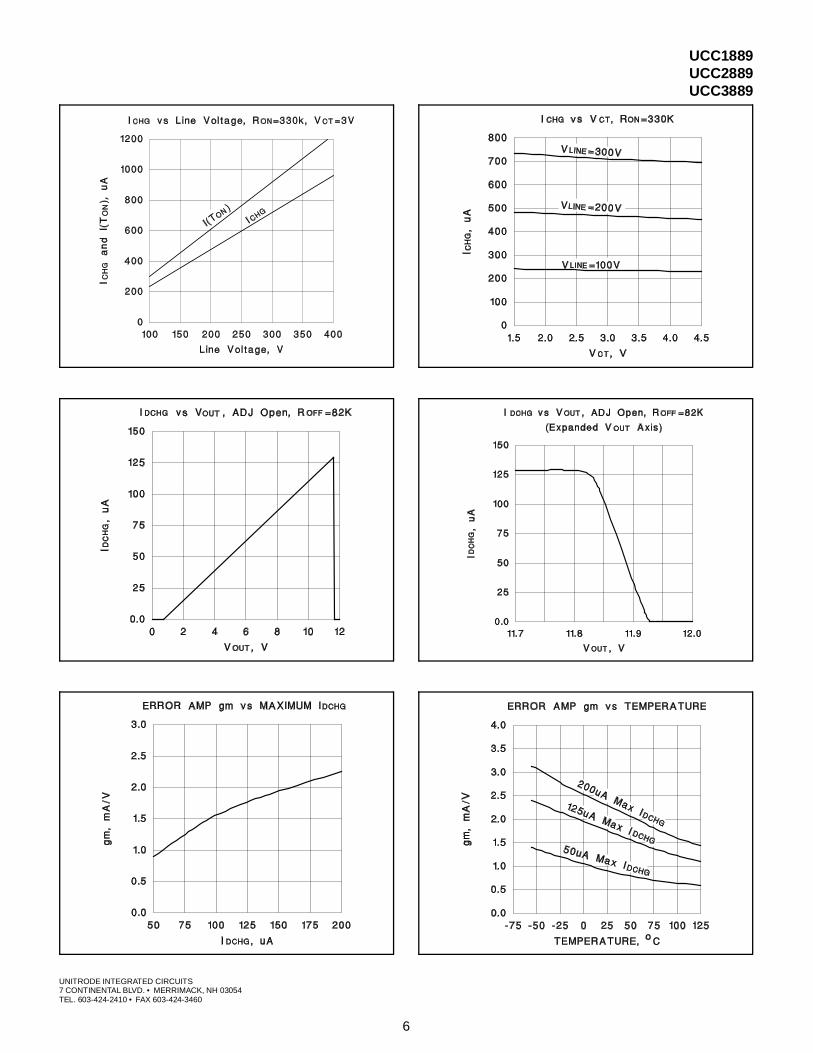
OPERATIONWith reference to the application diagram below, when input voltage is first applied,the RON current into TON is directed to VCC where it charges the external capacitor,C3, connected to VCC. As voltage builds on VCC, an internal undervoltage lockoutholds the circuit off and the output at DRIVE low until VCC reaches 8.4V. At thistime, DRIVE goes high turning on the power switch, Q1, and redirecting the currentinto TON to the timing capacitor, CT. CT charges to a fixed threshold with a currentICHG=0.8 • (VIN - 4.5V)/RON. Since DRIVE will only be high for as long as CT
charges, the power switch on time will be inversely proportional to line voltage.This provides a constant line voltage-switch on time product.
Note: This device incorporates patented technology used under license from Lambda Electronics, Inc.
TYPICAL APPLICATION
UDG-93060-1
UCC1889UCC2889UCC3889
OPERATION (cont.)At the end of the on time, Q1 is turned off and the RON
current into TON is again diverted to VCC. Thus the cur-rent through RON, which charges CT during the on time,contributes to supplying control power during the off time.
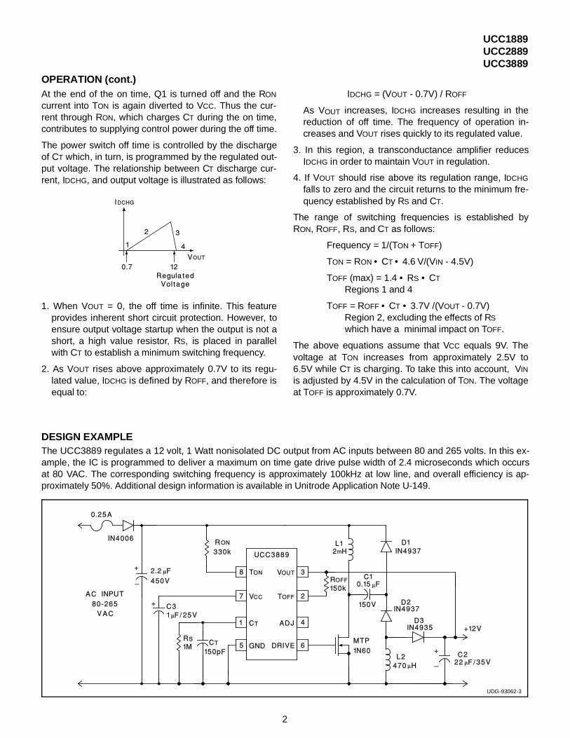
The power switch off time is controlled by the dischargeof CT which, in turn, is programmed by the regulated out-put voltage. The relationship between CT discharge cur-rent, IDCHG, and output voltage is illustrated as follows:
1. When VOUT = 0, the off time is infinite. This featureprovides inherent short circuit protection. However, toensure output voltage startup when the output is not ashort, a high value resistor, RS, is placed in parallelwith CT to establish a minimum switching frequency.
2. As VOUT rises above approximately 0.7V to its regu-lated value, IDCHG is defined by ROFF, and therefore isequal to:
IDCHG = (VOUT - 0.7V) / ROFF
As VOUT increases, IDCHG increases resulting in thereduction of off time. The frequency of operation in-creases and VOUT rises quickly to its regulated value.
3. In this region, a transconductance amplifier reducesIDCHG in order to maintain VOUT in regulation.
4. If VOUT should rise above its regulation range, IDCHG
falls to zero and the circuit returns to the minimum fre-quency established by RS and CT.
The range of switching frequencies is established byRON, ROFF, RS, and CT as follows:
Frequency = 1/(TON + TOFF)
TON = RON • CT • 4.6 V/(VIN - 4.5V)
TOFF (max) = 1.4 • RS • CT Regions 1 and 4
TOFF = ROFF • CT • 3.7V /(VOUT - 0.7V) Region 2, excluding the effects of RS
which have a minimal impact on TOFF.
The above equations assume that VCC equals 9V. Thevoltage at TON increases from approximately 2.5V to6.5V while CT is charging. To take this into account, VIN
is adjusted by 4.5V in the calculation of TON. The voltageat TOFF is approximately 0.7V.
DESIGN EXAMPLEThe UCC3889 regulates a 12 volt, 1 Watt nonisolated DC output from AC inputs between 80 and 265 volts. In this ex-ample, the IC is programmed to deliver a maximum on time gate drive pulse width of 2.4 microseconds which occursat 80 VAC. The corresponding switching frequency is approximately 100kHz at low line, and overall efficiency is ap-proximately 50%. Additional design information is available in Unitrode Application Note U-149.
UDG-93062-3
2

PARAMETER TEST CONDITIONS MIN TYP MAX UNITS
General VCC Zener Voltage ICC < 1.5mA 8.6 9.0 9.3 V
Startup Current VOUT = 0 150 250 µA
Operating Current I(VOUT) VOUT = 11V, F = 150kHz 1.2 2.5 mA
Under-Voltage-LockoutStart Threshold VOUT = 0 8.0 8.4 8.8 V
Minimum Operating Voltage after Start VOUT = 0 6.0 6.3 6.6 V
Hysteresis VOUT = 0 1.8 V
OscillatorAmplitude VCC = 9V 3.5 3.7 3.9 V
CT to DRIVE high Propagation Delay Overdrive = 0.2V 100 200 ns
CT to DRIVE low Propagation Delay Overdrive = 0.2V 50 100 ns
DriverVOL I = 20mA, VCC = 9V 0.15 0.4 V
I = 100mA, VCC = 9V 0.7 1.8 V
VOH I = −20mA, VCC = 9V 8.5 8.8 V
I = −100mA, VCC = 9V 6.1 7.8 V
Rise Time CLOAD = 1nF 35 70 ns
Fall Time CLOAD = 1nF 30 60 ns
Line Voltage Detection
Charge Coefficient: ICHG / I(TON) VCT = 3V, DRIVE = High, I(TON) = 1mA 0.73 0.79 0.85
Minimum Line Voltage for Fault RON = 330k 60 80 100 V
Minimum Current I(TON) for Fault RON = 330k 220 µA
On Time During Fault CT = 150pF, VLINE = Min − 1V 2 µs
Oscillator Restart Delay after Fault 0.5 ms
VOUT Error AmpVOUT Regulated 12V (ADJ Open) VCC = 9V, IDCHG = I(TOFF)/2 11.2 11.9 12.8 V
VOUT Regulated 18V (ADJ = 0V) VCC = 9V, IDCHG = I(TOFF)/2 16.5 17.5 19.5 V
Discharge Ratio: IDCHG / I(TOFF) I(TOFF) = 50µA 0.93 1.00 1.07
Voltage at TOFF I(TOFF) = 50µA 0.6 0.95 1.3 V
Regulation gm (Note 1) Max IDCHG = 50µA 1.0 mA/V
Max IDCHG = 125µA 0.8 1.7 2.9 mA/V
Unless otherwise stated, these specifications hold for TA = 0°C to 70°C for theUCC3889, -40°C to +85°C for the UCC2889, and -55°C to +125°C for the UCC1889.No load at DRIVE pin (CLOAD=0).
ELECTRICAL CHARACTERISTICS
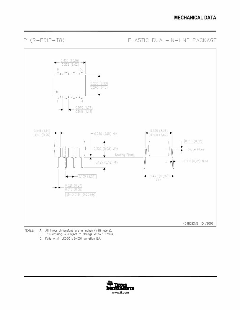
DIL-8, SOIC-8 (Top View)N or J, D Package
CONNECTION DIAGRAMICC. . . . . . . . . . . . . . . . . . . . . . . . . . . . . . . . . . . . . . . . . . . . 5mACurrent into TON Pin . . . . . . . . . . . . . . . . . . . . . . . . . . . . . 1.5mAVoltage on VOUT Pin. . . . . . . . . . . . . . . . . . . . . . . . . . . . . . . 20VCurrent into TOFF Pin . . . . . . . . . . . . . . . . . . . . . . . . . . . . 250µAStorage Temperature . . . . . . . . . . . . . . . . . . . . -65°C to +150°CNote: Unless otherwise indicated, voltages are referenced toground and currents are positive into, negative out of, the speci-fied terminals.
ABSOLUTE MAXIMUM RATINGS
UCC1889UCC2889UCC3889
Note 1: gm is defined as ∆IDCHG
∆VOUT for the values of VOUT when VOUT is in regulation. The two points used to calculate gm are for
IDCHG at 65% and 35% of its maximum value.
3
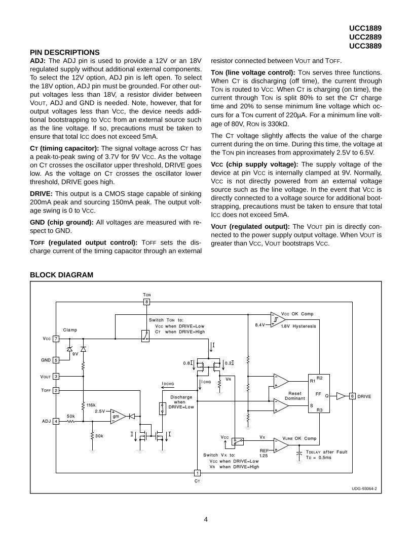
ADJ: The ADJ pin is used to provide a 12V or an 18Vregulated supply without additional external components.To select the 12V option, ADJ pin is left open. To selectthe 18V option, ADJ pin must be grounded. For other out-put voltages less than 18V, a resistor divider betweenVOUT, ADJ and GND is needed. Note, however, that foroutput voltages less than VCC, the device needs addi-tional bootstrapping to VCC from an external source suchas the line voltage. If so, precautions must be taken toensure that total ICC does not exceed 5mA.
CT (timing capacitor): The signal voltage across CT hasa peak-to-peak swing of 3.7V for 9V VCC. As the voltageon CT crosses the oscillator upper threshold, DRIVE goeslow. As the voltage on CT crosses the oscillator lowerthreshold, DRIVE goes high.
DRIVE: This output is a CMOS stage capable of sinking200mA peak and sourcing 150mA peak. The output volt-age swing is 0 to VCC.
GND (chip ground): All voltages are measured with re-spect to GND.
TOFF (regulated output control): TOFF sets the dis-charge current of the timing capacitor through an external
resistor connected between VOUT and TOFF.
TON (line voltage control): TON serves three functions.When CT is discharging (off time), the current throughTON is routed to VCC. When CT is charging (on time), thecurrent through TON is split 80% to set the CT chargetime and 20% to sense minimum line voltage which oc-curs for a TON current of 220µA. For a minimum line volt-age of 80V, RON is 330kΩ.
The CT voltage slightly affects the value of the chargecurrent during the on time. During this time, the voltage atthe TON pin increases from approximately 2.5V to 6.5V.
VCC (chip supply voltage): The supply voltage of thedevice at pin VCC is internally clamped at 9V. Normally,VCC is not directly powered from an external voltagesource such as the line voltage. In the event that VCC isdirectly connected to a voltage source for additional boot-strapping, precautions must be taken to ensure that totalICC does not exceed 5mA.
VOUT (regulated output): The VOUT pin is directly con-nected to the power supply output voltage. When VOUT isgreater than VCC, VOUT bootstraps VCC.
UCC1889UCC2889UCC3889
PIN DESCRIPTIONS
BLOCK DIAGRAM
UDG-93064-2
4
UCC1889UCC2889UCC3889
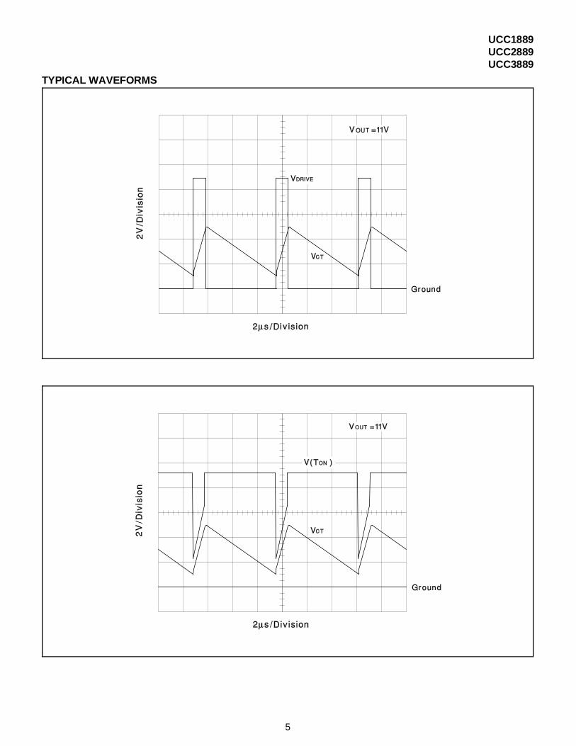
TYPICAL WAVEFORMS
5
UNITRODE INTEGRATED CIRCUITS7 CONTINENTAL BLVD. • MERRIMACK, NH 03054TEL. 603-424-2410 • FAX 603-424-3460
UCC1889UCC2889UCC3889
6
PACKAGE OPTION ADDENDUM
www.ti.com 13-Aug-2021
Addendum-Page 1
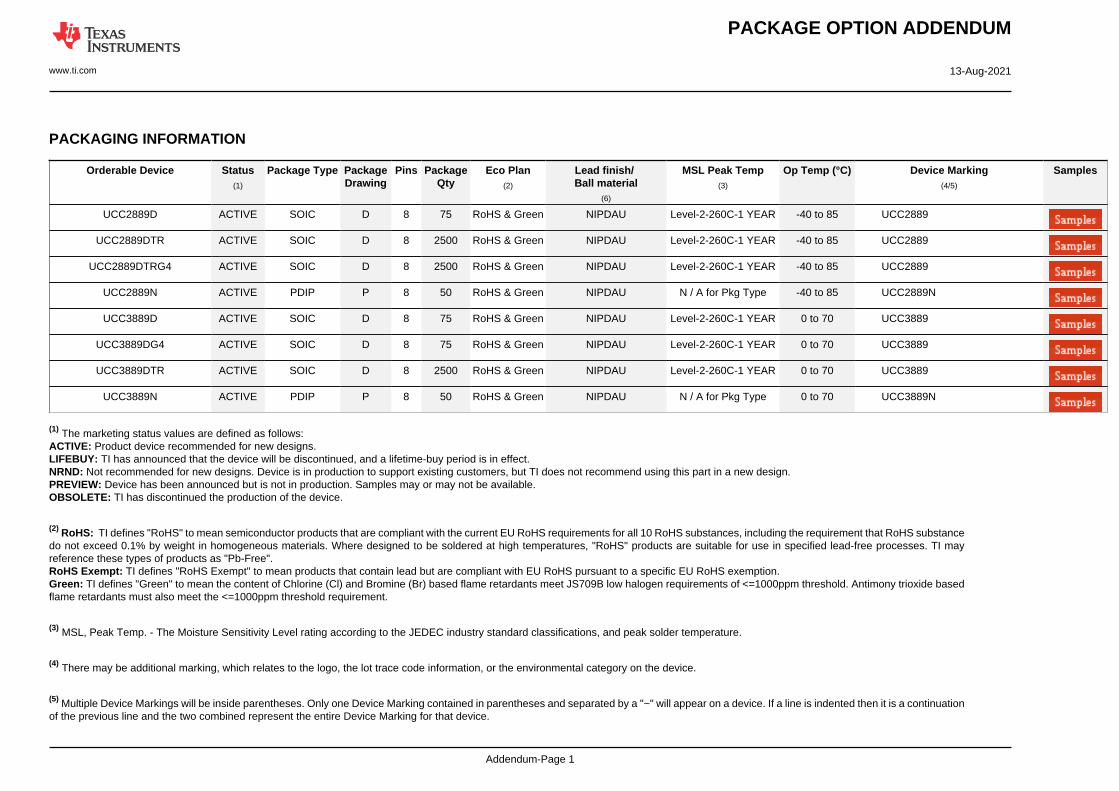
PACKAGING INFORMATION
Orderable Device Status(1)
Package Type PackageDrawing
Pins PackageQty
Eco Plan(2)
Lead finish/Ball material
(6)
MSL Peak Temp(3)
Op Temp (°C) Device Marking(4/5)
Samples
UCC2889D ACTIVE SOIC D 8 75 RoHS & Green NIPDAU Level-2-260C-1 YEAR -40 to 85 UCC2889
UCC2889DTR ACTIVE SOIC D 8 2500 RoHS & Green NIPDAU Level-2-260C-1 YEAR -40 to 85 UCC2889
UCC2889DTRG4 ACTIVE SOIC D 8 2500 RoHS & Green NIPDAU Level-2-260C-1 YEAR -40 to 85 UCC2889
UCC2889N ACTIVE PDIP P 8 50 RoHS & Green NIPDAU N / A for Pkg Type -40 to 85 UCC2889N
UCC3889D ACTIVE SOIC D 8 75 RoHS & Green NIPDAU Level-2-260C-1 YEAR 0 to 70 UCC3889
UCC3889DG4 ACTIVE SOIC D 8 75 RoHS & Green NIPDAU Level-2-260C-1 YEAR 0 to 70 UCC3889
UCC3889DTR ACTIVE SOIC D 8 2500 RoHS & Green NIPDAU Level-2-260C-1 YEAR 0 to 70 UCC3889
UCC3889N ACTIVE PDIP P 8 50 RoHS & Green NIPDAU N / A for Pkg Type 0 to 70 UCC3889N
(1) The marketing status values are defined as follows:ACTIVE: Product device recommended for new designs.LIFEBUY: TI has announced that the device will be discontinued, and a lifetime-buy period is in effect.NRND: Not recommended for new designs. Device is in production to support existing customers, but TI does not recommend using this part in a new design.PREVIEW: Device has been announced but is not in production. Samples may or may not be available.OBSOLETE: TI has discontinued the production of the device.
(2) RoHS: TI defines "RoHS" to mean semiconductor products that are compliant with the current EU RoHS requirements for all 10 RoHS substances, including the requirement that RoHS substancedo not exceed 0.1% by weight in homogeneous materials. Where designed to be soldered at high temperatures, "RoHS" products are suitable for use in specified lead-free processes. TI mayreference these types of products as "Pb-Free".RoHS Exempt: TI defines "RoHS Exempt" to mean products that contain lead but are compliant with EU RoHS pursuant to a specific EU RoHS exemption.Green: TI defines "Green" to mean the content of Chlorine (Cl) and Bromine (Br) based flame retardants meet JS709B low halogen requirements of <=1000ppm threshold. Antimony trioxide basedflame retardants must also meet the <=1000ppm threshold requirement.
(3) MSL, Peak Temp. - The Moisture Sensitivity Level rating according to the JEDEC industry standard classifications, and peak solder temperature.
(4) There may be additional marking, which relates to the logo, the lot trace code information, or the environmental category on the device.
(5) Multiple Device Markings will be inside parentheses. Only one Device Marking contained in parentheses and separated by a "~" will appear on a device. If a line is indented then it is a continuationof the previous line and the two combined represent the entire Device Marking for that device.
PACKAGE OPTION ADDENDUM
www.ti.com 13-Aug-2021
Addendum-Page 2
(6) Lead finish/Ball material - Orderable Devices may have multiple material finish options. Finish options are separated by a vertical ruled line. Lead finish/Ball material values may wrap to twolines if the finish value exceeds the maximum column width.
Important Information and Disclaimer:The information provided on this page represents TI's knowledge and belief as of the date that it is provided. TI bases its knowledge and belief on informationprovided by third parties, and makes no representation or warranty as to the accuracy of such information. Efforts are underway to better integrate information from third parties. TI has taken andcontinues to take reasonable steps to provide representative and accurate information but may not have conducted destructive testing or chemical analysis on incoming materials and chemicals.TI and TI suppliers consider certain information to be proprietary, and thus CAS numbers and other limited information may not be available for release.
In no event shall TI's liability arising out of such information exceed the total purchase price of the TI part(s) at issue in this document sold by TI to Customer on an annual basis.
TAPE AND REEL INFORMATION
*All dimensions are nominal
Device PackageType
PackageDrawing
Pins SPQ ReelDiameter
(mm)
ReelWidth
W1 (mm)
A0(mm)
B0(mm)
K0(mm)
P1(mm)
W(mm)
Pin1Quadrant
UCC2889DTR SOIC D 8 2500 330.0 12.4 6.4 5.2 2.1 8.0 12.0 Q1
UCC3889DTR SOIC D 8 2500 330.0 12.4 6.4 5.2 2.1 8.0 12.0 Q1
PACKAGE MATERIALS INFORMATION
www.ti.com 5-Jan-2022
Pack Materials-Page 1
*All dimensions are nominal
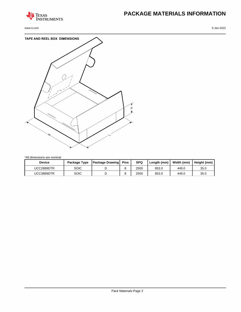
Device Package Type Package Drawing Pins SPQ Length (mm) Width (mm) Height (mm)
UCC2889DTR SOIC D 8 2500 853.0 449.0 35.0
UCC3889DTR SOIC D 8 2500 853.0 449.0 35.0
PACKAGE MATERIALS INFORMATION
www.ti.com 5-Jan-2022
Pack Materials-Page 2

TUBE
*All dimensions are nominal
Device Package Name Package Type Pins SPQ L (mm) W (mm) T (µm) B (mm)
UCC2889D D SOIC 8 75 506.6 8 3940 4.32
UCC2889N P PDIP 8 50 506 13.97 11230 4.32
UCC3889D D SOIC 8 75 506.6 8 3940 4.32
UCC3889DG4 D SOIC 8 75 506.6 8 3940 4.32
UCC3889N P PDIP 8 50 506 13.97 11230 4.32
PACKAGE MATERIALS INFORMATION
www.ti.com 5-Jan-2022
Pack Materials-Page 3
www.ti.com
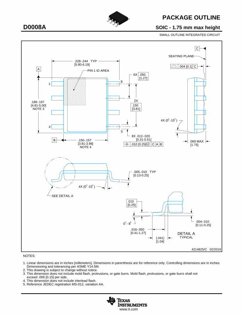
PACKAGE OUTLINE
C
.228-.244 TYP[5.80-6.19]
.069 MAX[1.75]
6X .050[1.27]
8X .012-.020 [0.31-0.51]
2X.150[3.81]
.005-.010 TYP[0.13-0.25]
0 - 8 .004-.010[0.11-0.25]
.010[0.25]
.016-.050[0.41-1.27]
4X (0 -15 )
A
.189-.197[4.81-5.00]
NOTE 3
B .150-.157[3.81-3.98]
NOTE 4
4X (0 -15 )
(.041)[1.04]
SOIC - 1.75 mm max heightD0008ASMALL OUTLINE INTEGRATED CIRCUIT
4214825/C 02/2019
NOTES: 1. Linear dimensions are in inches [millimeters]. Dimensions in parenthesis are for reference only. Controlling dimensions are in inches. Dimensioning and tolerancing per ASME Y14.5M. 2. This drawing is subject to change without notice. 3. This dimension does not include mold flash, protrusions, or gate burrs. Mold flash, protrusions, or gate burrs shall not exceed .006 [0.15] per side. 4. This dimension does not include interlead flash.5. Reference JEDEC registration MS-012, variation AA.
18
.010 [0.25] C A B
54
PIN 1 ID AREA
SEATING PLANE
.004 [0.1] C
SEE DETAIL A
DETAIL ATYPICAL
SCALE 2.800

www.ti.com
EXAMPLE BOARD LAYOUT
.0028 MAX[0.07]ALL AROUND
.0028 MIN[0.07]ALL AROUND
(.213)[5.4]
6X (.050 )[1.27]
8X (.061 )[1.55]
8X (.024)[0.6]
(R.002 ) TYP[0.05]
SOIC - 1.75 mm max heightD0008ASMALL OUTLINE INTEGRATED CIRCUIT
4214825/C 02/2019
NOTES: (continued) 6. Publication IPC-7351 may have alternate designs. 7. Solder mask tolerances between and around signal pads can vary based on board fabrication site.
METALSOLDER MASKOPENING
NON SOLDER MASKDEFINED
SOLDER MASK DETAILS
EXPOSEDMETAL
OPENINGSOLDER MASK METAL UNDER
SOLDER MASK
SOLDER MASKDEFINED
EXPOSEDMETAL
LAND PATTERN EXAMPLEEXPOSED METAL SHOWN
SCALE:8X
SYMM
1
45
8
SEEDETAILS
SYMM

www.ti.com
EXAMPLE STENCIL DESIGN
8X (.061 )[1.55]
8X (.024)[0.6]
6X (.050 )[1.27]
(.213)[5.4]
(R.002 ) TYP[0.05]
SOIC - 1.75 mm max heightD0008ASMALL OUTLINE INTEGRATED CIRCUIT
4214825/C 02/2019
NOTES: (continued) 8. Laser cutting apertures with trapezoidal walls and rounded corners may offer better paste release. IPC-7525 may have alternate design recommendations. 9. Board assembly site may have different recommendations for stencil design.
SOLDER PASTE EXAMPLEBASED ON .005 INCH [0.125 MM] THICK STENCIL
SCALE:8X
SYMM
SYMM
1
45
8
IMPORTANT NOTICE AND DISCLAIMERTI PROVIDES TECHNICAL AND RELIABILITY DATA (INCLUDING DATA SHEETS), DESIGN RESOURCES (INCLUDING REFERENCE DESIGNS), APPLICATION OR OTHER DESIGN ADVICE, WEB TOOLS, SAFETY INFORMATION, AND OTHER RESOURCES “AS IS” AND WITH ALL FAULTS, AND DISCLAIMS ALL WARRANTIES, EXPRESS AND IMPLIED, INCLUDING WITHOUT LIMITATION ANY IMPLIED WARRANTIES OF MERCHANTABILITY, FITNESS FOR A PARTICULAR PURPOSE OR NON-INFRINGEMENT OF THIRD PARTY INTELLECTUAL PROPERTY RIGHTS.These resources are intended for skilled developers designing with TI products. You are solely responsible for (1) selecting the appropriate TI products for your application, (2) designing, validating and testing your application, and (3) ensuring your application meets applicable standards, and any other safety, security, regulatory or other requirements.These resources are subject to change without notice. TI grants you permission to use these resources only for development of an application that uses the TI products described in the resource. Other reproduction and display of these resources is prohibited. No license is granted to any other TI intellectual property right or to any third party intellectual property right. TI disclaims responsibility for, and you will fully indemnify TI and its representatives against, any claims, damages, costs, losses, and liabilities arising out of your use of these resources.TI’s products are provided subject to TI’s Terms of Sale or other applicable terms available either on ti.com or provided in conjunction with such TI products. TI’s provision of these resources does not expand or otherwise alter TI’s applicable warranties or warranty disclaimers for TI products.TI objects to and rejects any additional or different terms you may have proposed. IMPORTANT NOTICE
Mailing Address: Texas Instruments, Post Office Box 655303, Dallas, Texas 75265Copyright © 2022, Texas Instruments Incorporated