ubsc/bbsc/ulsc 60 /40/20 ghz ultra broadband silicon ...€¦ · assembly by soldering the...
TRANSCRIPT
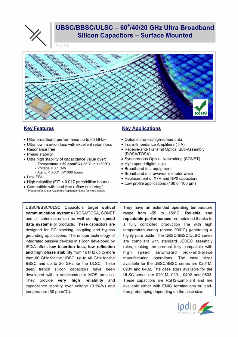
UBSC/BBSC/ULSC – 60+/40/20 GHz Ultra Broadband
Silicon Capacitors – Surface Mounted
Rev 3.0
Key Features Key Applications
UBSC/BBSC/ULSC Capacitors target optical
communication systems (ROSA/TOSA, SONET
and all optoelectronics) as well as high speed
data systems or products. These capacitors are
designed for DC blocking, coupling and bypass
grounding applications. The unique technology of
integrated passive devices in silicon developed by
IPDiA offers low insertion loss, low reflection
and high phase stability from 16 kHz up to more
than 60 GHz for the UBSC, up to 40 GHz for the
BBSC and up to 20 GHz for the ULSC. These
deep trench silicon capacitors have been
developed with a semiconductor MOS process.
They provide very high reliability and
capacitance stability over voltage (0.1%/V) and
temperature (50 ppm/°C).
They have an extended operating temperature
range from -55 to 150°C. Reliable and
repeatable performances are obtained thanks to
a fully controlled production line with high
temperature curing (above 900°C) generating a
highly pure oxide. The UBSC/BBSC/ULSC series
are compliant with standard JEDEC assembly
rules, making the product fully compatible with
high speed automated pick-and-place
manufacturing operations. The case sizes
available for the UBSC/BBSC series are 0201M,
0201 and 0402. The case sizes available for the
ULSC series are 0201M, 0201, 0402 and 0603.
These capacitors are RoHS-compliant and are
available either with ENIG terminations or lead-
free prebumping depending on the case size.
Ultra broadband performance up to 60 GHz+
Ultra low insertion loss with excellent return loss
Resonance free
Phase stability
Ultra high stability of capacitance value over: - Temperature < 50 ppm/°C (-55°C to +150°C)
- Voltage < 0.1 %/V - Aging < 0.001 %/1000 hours
Low ESL
High reliability (FIT < 0.017 parts/billion hours)
Compatible with lead free reflow-soldering* * Please refer to our Assembly Application Note for more details
Optoelectronics/high-speed data
Trans-Impedance Amplifiers (TIA)
Receive-and-Transmit Optical Sub-Assembly (ROSA/TOSA)
Synchronous Optical Networking (SONET)
High speed digital logic
Broadband test equipment
Broadband microwave/millimeter wave
Replacement of X7R and NP0 capacitors
Low profile applications (400 or 100 µm)
IPDiA Capacitors – UBSC Series
UBSC 60 GHz+ Electrical Specifications
UBSC 60 GHz+ Capacitance Range
UBSC 60 GHz+ Termination and Outline
L
T
W
b
a
c
Termination Lead-free nickel/solder coating compatible with automatic soldering technologies: reflow and manual.
Package Outline For landing pad dimensions on your PCB layout, please refer to IPDiA assembly application note.
UBSC 60 GHz+ Packaging
Tape and reel, waffle pack, film frame carrier or raw wafer delivery.
Available parts – see table above For other values, contact your IPDiA sales representative.
Part number Product description Case Size Thickness
UBSC.xxx Surface Mount Ultra Broad Band Silicon Capacitor from -55 to 150°C, 60 GHz with ENIG termination
935 152 492 510(*) Ultra Broadband Si Cap 10 nF 60 GHz+100 µm, BV>11 V 0201M 100 µm
935 151 723 510 Ultra Broadband Si Cap 10 nF 60 GHz+ 400 µm, BV>30 V 0201 400 µm
935 152 723 510 Ultra Broadband Si Cap 10 nF 60 GHz+ 100 µm, BV>30 V 0201 100 µm
935 151 424 610 Ultra Broadband Si Cap 100 nF 60 GHz+ 400 µm, BV>11 V 0402 400 µm
935 152 424 610 Ultra Broadband Si Cap 100 nF 60 GHz+ 100 µm, BV>11 V 0402 100 µm
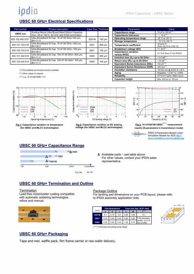
Fig.1: Capacitance variation vs temperature
(for UBSC and MLCC technologies)
Fig.2: Capacitance variation vs DC biasing voltage (for UBSC and MLCC technologies)
Fig.3: 10 nF/0201M UBSC(***)
measurement
results (S-parameters in transmission mode)
Parameters Value Capacitance range 10 nF to 100 nF(**) Capacitance tolerance ± 15 %(**) Operating temperature range -55 °C to 150 °C Storage temperature - 70 °C to 165 °C
Temperature coefficient 50 ppm/°C (from -55 °C to +150 °C)
Breakdown voltage (BV) 11, 30 V(**) Capacitance variation versus RVDC 0.1 %/V (from 0 V to RVDC)
Insertion loss (IL) up to 60 GHz+ < 0.4 dB(***) Return loss (RL) up to 60 GHz+ > 20 dB(***) Equivalent Series Inductance (ESL) 100 pH(***) Equivalent Series Resistance (ESR) 300 m
(***) Insulation resistance 100 G min @ RVDC & +25°C Aging Negligible, < 0.001 % / 1000h Reliability FIT<0.017 parts / billion hours Capacitor height Max 400 µm or 100 µm
(*) Only leadfree pre-bumped version available
(**) Other values on request
(***) e.g. 10 nF/0201M/BV 11V
FREE S-Parameters-Based Linear Simulation Models for ADS:http://www.modelithics.com/mvpIpdia.asp
(mm) Pad dimensions Case size (typ. ±0.01 mm) a b c L W T(****)
0201M 0.1 0.15 0.2 0.60 0.30 0.1
0201 0.15 0.40 0.30 0.80 0.60 0.40 (standard profile) or 0.10
(low profile) 0402 0.30 0.50 0.40 1.20 0.70
(****) Thickness excluding bump height
IPDiA Capacitors – BBSC Series
BBSC 40 GHz Electrical Specifications
BBSC 40 GHz Capacitance Range
BBSC 40 GHz Termination and Outline
L
T
W
b
a
c
Termination Lead-free nickel/solder coating compatible with automatic soldering technologies: reflow and manual.
Package Outline For landing pad dimensions on your PCB layout, please refer to IPDiA assembly application note.
BBSC 40 GHz Packaging
Tape and reel, waffle pack, film frame carrier or raw wafer delivery.
Available parts – see table above For other values, contact your IPDiA sales representative.
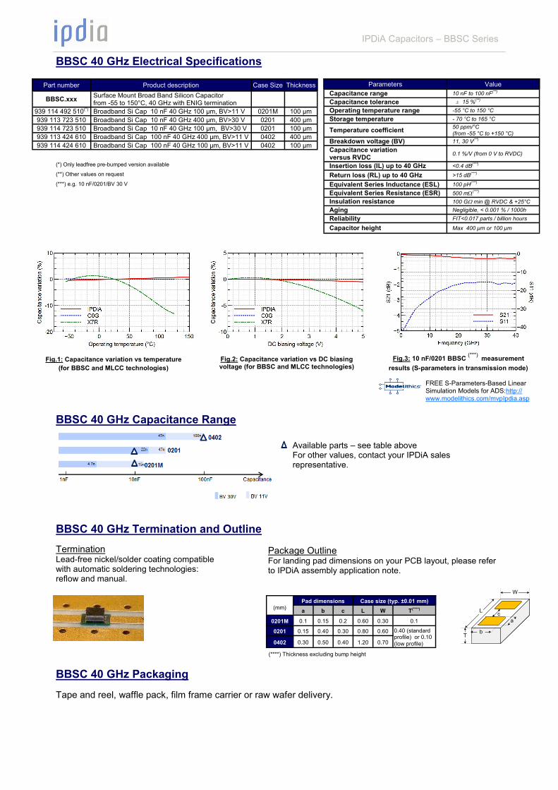
Fig.1: Capacitance variation vs temperature
(for BBSC and MLCC technologies)
Fig.2: Capacitance variation vs DC biasing voltage (for BBSC and MLCC technologies)
Fig.3: 10 nF/0201 BBSC (***)
measurement
results (S-parameters in transmission mode)
FREE S-Parameters-Based Linear Simulation Models for ADS:http://www.modelithics.com/mvpIpdia.asp
(mm) Pad dimensions Case size (typ. ±0.01 mm) a b c L W T(****)
0201M 0.1 0.15 0.2 0.60 0.30 0.1
0201 0.15 0.40 0.30 0.80 0.60 0.40 (standard profile) or 0.10
(low profile) 0402 0.30 0.50 0.40 1.20 0.70
Part number Product description Case Size Thickness
BBSC.xxx Surface Mount Broad Band Silicon Capacitor from -55 to 150°C, 40 GHz with ENIG termination
939 114 492 510(*) Broadband Si Cap 10 nF 40 GHz 100 µm, BV>11 V 0201M 100 µm 939 113 723 510 Broadband Si Cap 10 nF 40 GHz 400 µm, BV>30 V 0201 400 µm 939 114 723 510 Broadband Si Cap 10 nF 40 GHz 100 µm, BV>30 V 0201 100 µm 939 113 424 610 Broadband Si Cap 100 nF 40 GHz 400 µm, BV>11 V 0402 400 µm 939 114 424 610 Broadband Si Cap 100 nF 40 GHz 100 µm, BV>11 V 0402 100 µm
Parameters Value Capacitance range 10 nF to 100 nF(**) Capacitance tolerance ± 15 %(**) Operating temperature range -55 °C to 150 °C Storage temperature - 70 °C to 165 °C
Temperature coefficient 50 ppm/°C (from -55 °C to +150 °C)
Breakdown voltage (BV) 11, 30 V(**) Capacitance variation versus RVDC 0.1 %/V (from 0 V to RVDC)
Insertion loss (IL) up to 40 GHz <0.4 dB(***) Return loss (RL) up to 40 GHz >15 dB(***) Equivalent Series Inductance (ESL) 100 pH(***) Equivalent Series Resistance (ESR) 500 m
(***) Insulation resistance 100 G min @ RVDC & +25°C Aging Negligible, < 0.001 % / 1000h Reliability FIT<0.017 parts / billion hours Capacitor height Max 400 µm or 100 µm
(*) Only leadfree pre-bumped version available
(**) Other values on request
(***) e.g. 10 nF/0201/BV 30 V
(****) Thickness excluding bump height
IPDiA Capacitors – ULSC Series
ULSC 20 GHz Electrical Specifications
ULSC 20 GHz Capacitance Range
ULSC 20 GHz Termination and Outline
L
T
W
b
a
c
Termination Lead-free nickel/solder coating compatible with automatic soldering technologies: reflow and manual.
Package Outline For landing pad dimensions on your PCB layout, please refer to IPDiA assembly application note.
ULSC 20 GHz Packaging
Tape and reel, waffle pack, film frame carrier or raw wafer delivery.
Available parts – see table above For other values, contact your IPDiA sales representative.
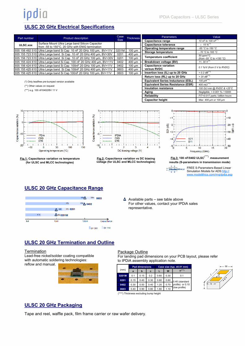
Fig.1: Capacitance variation vs temperature
(for ULSC and MLCC technologies)
Fig.2: Capacitance variation vs DC biasing voltage (for ULSC and MLCC technologies)
FREE S-Parameters-Based Linear Simulation Models for ADS:http://www.modelithics.com/mvpIpdia.asp
Part number Product description Case Size Thickness
ULSC.xxx Surface Mount Ultra Large band Silicon Capacitor from -55 to 150°C, 20 GHz with ENIG termination
935 156 492 510 Ultra Large band Si Cap 10 nF 20 GHz 100 µm, BV>11V 0201M 100 µm 935 155 723 510 Ultra Large band Si Cap 10 nF 20 GHz 400 µm, BV>30V 0201 400 µm 935 156 723 510 Ultra Large band Si Cap 10 nF 20 GHz 100 µm, BV>30V 0201 100 µm 935 155 424 610 Ultra Large band Si Cap 100 nF 20 GHz 400 µm, BV>11V 0402 400 µm 935 156 424 610 Ultra Large band Si Cap 100nF 20 GHz 100 µm, BV>11V 0402 100 µm 935 155 425 610 Ultra Large band Si Cap 100nF 20 GHz 400 µm, BV>11V 0603 400 µm 935 156 425 610 Ultra Large band Si Cap 100nF 20 GHz 100 µm, BV>11V 0603 100 µm
(*) Only leadfree pre-bumped version available
(**) Other values on request
(***) e.g. 100 nF/0402/BV 11 V
Parameters Value Capacitance range 10 nF to 100 nF(**) Capacitance tolerance ± 15 %(**) Operating temperature range -55 °C to 150 °C Storage temperature - 70 °C to 165 °C
Temperature coefficient 50 ppm/°C (from -55 °C to +150 °C)
Breakdown voltage (BV) 11, 30 V(**) Capacitance variation versus RVDC 0.1 %/V (from 0 V to RVDC)
Insertion loss (IL) up to 20 GHz < 0.2 dB(***) Return loss (RL) up to 20 GHz > 20 dB(***) Equivalent Series Inductance (ESL) 100 pH(***) Equivalent Series Resistance (ESR) 400 m
(***) Insulation resistance 100 G min @ RVDC & +25°C Aging Negligible, < 0.001 % / 1000h Reliability FIT<0.017 parts / billion hours Capacitor height Max 400 µm or 100 µm
Fig.3: 100 nF/0402 ULSC(***)
measurement
results (S-parameters in transmission mode)
(mm) Pad dimensions Case size (typ. ±0.01 mm) a b c L W T(****)
0201M 0.1 0.15 0.2 0.60 0.30 0.1
0201 0.15 0.40 0.30 0.80 0.60 0.40 (standard profile) or 0.10
(low profile) 0402 0.30 0.50 0.40 1.20 0.70 0603 0.40 0.90 0.80 1.80 1.10
(****) Thickness excluding bump height
Reproduction in whole or in part is prohibited without the prior written
consent of the copyright owner. The information presented in this
document does not form part of any quotation or contract, is believed to
be accurate and reliable and may be changed without notice. No
liability will be accepted by the publisher for any consequence of its
use. Publication thereof does not convey nor imply any license under
patent- or other industrial or intellectual property rights.
For more information, please visit: http://www.ipdia.com To contact us, email to: [email protected]
Date of release: 01/06/2016
Document identifier: CL
IPDiA Capacitors – Assembly by Soldering
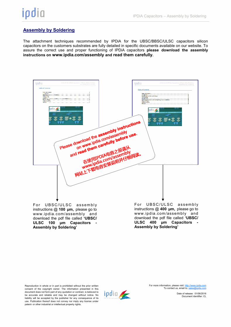
Assembly by Soldering
The attachment techniques recommended by IPDiA for the UBSC/BBSC/ULSC capacitors silicon capacitors on the customers substrates are fully detailed in specific documents available on our website. To assure the correct use and proper functioning of IPDiA capacitors please download the assembly
instructions on www.ipdia.com/assembly and read them carefully.
F o r U BSC / U L SC a s s em b l y instructions @ 100 µm, please go to www. ipdia.com/assembly and download the pdf file called ‘UBSC/ULSC 100 µm Capacitors - Assembly by Soldering’
F o r U BSC / U L SC a s s em b l y instructions @ 400 µm, please go to www. ipdia.com/assembly and download the pdf file called ‘UBSC/ULSC 400 µm Capacitors - Assembly by Soldering’