two print stencil systems - circuitinsight.com · (1), pin placed in the through-hole (2) and pin...
TRANSCRIPT

Two Print Stencils Systems
William E. Coleman
Photo Stencil
Colorado Springs, CO
Abstract
The Two print stencils process has been a very useful tool in SMT Assembly and Package Assembly. It is also useful in
Assemblies that require mixed technologies; including SMT / Through Hole, SMT / Glue attach components, Packages
requiring die attach / SMT assembly. The concept is to print with a first print stencil which is thinner than the second print
stencil. The second print stencil has relief pockets formed anywhere that the first stencil printed. It is useful for several
applications:
Printing Solder Paste for Through-Hole and SMT
Printing Glue and Solder Paste
Printing Flux and Solder Paste
Printing Solder Paste for SMT and RF Shields
Printing Reservoir Solder Paste for multi-level boards
Printing Solder Paste and Reservoir Flux
Each of these applications will be discussed in this presentation.
Introduction
One of the first requirements (mid 1990’s) for Two Print stencils was Intrusive Reflow of a fully populated Pin-Grid-Array.
The volume of solder paste required to form a sufficient fillet for the Through-Hole required a very thick stencil, so thick that
a normal step stencil was not a practical solution. The first print stencil was 6 mils thick and printed solder paste for the SMT
devices. The second print stencil was 16 mils thick and had a relief pocket 10 mils deep for the first print solder paste. Not
long after that, there was an application for printing solder paste first, then glue for large chip components that needed to be
glued during second pass reflow. In the late 1990’s a microprocessor package assembly required a thin layer of flux to be
printed for die attach, then solder paste for decoupling capacitors. A two print process having a 2 mil thick first print stencil
for the flux and a 6 mil thick stencil for the SMT chip components with relief pocket for the flux worked well for this
application. In 2007 an application appeared for printing into a two level board where the SMT component pads were
recessed 12 mils below the top surface of the PCB. The SMT pads were very close to the walls of the recessed area. A step
stencil was manufactured that fit into the board cavity with a reservoir for paste above the apertures. The paste was delivered
to the SMT pads by Reservoir printing. Very recently, an application for assembling die attach and 01005 on the same
substrate presented itself. The stencil design for this application required a two print process involving flux reservoir
printing. Stencils for these application opportunities will be described in this presentation.
Stencil Design for Intrusive Reflow of Through- Hole Components
Sometimes it is desirable to by-pass the wave solder operation and print solder paste for both SMT and Through-Hole
devices(1)
. After solder paste is printed both the SMT and Through-Hole devices are placed and both reflowed at the same
time. The first task in designing a stencil for this application is to determine the amount of solder paste required to fill solder
paste in and around the pins and form a proper solder fillet around the pins. The first option is to see if enlarging the stencil
aperture to overprint around the Through-Hole will provide sufficient solder; if not, then look at a step-up stencil with
overprint; if still insufficient look at a Two Print Stencil Process. Figure 1 shows solder paste bricks printed on the PCB for
an Axial Resistor Through-Hole for an overprinted aperture in a 6 mil thick stencil. The stencil provided sufficient solder
paste for good solder fill around the pin and good pin fillet as evidences in Figure 2 (an X-RAY cross section of the pin in the
PCB after reflow). In the case of a fully populated Through-Hole connector the amount of paste overprint is limited. This is
shown in Figure 3 where the overprint aperture is limited to 85 mils square on a 100 mil pitch. In this case a Two Print
Stencil system may be required which is shown in Figure 4. The paste delivered is made up of two parts; hole fill paste and
overprint paste. Both components are shown in the X-RAY picture shown in Figure 5. This sequence shows paste printed in
(1), pin placed in the Through-Hole (2) and Pin with solder after reflow. Pin to Hole ratio is also important as seen in Figure
6 Pin-to-Hole ratios of .56 and less were exhibiting voids.
Printing Glue and Solder Paste
There are some applications where heavy parts like large Chip components or SMT leaded components are placed on the
back side of the PCB in a single reflow operation. These large components may need to be glued. When stencil printing
glue, a Two Print Stencil Process must be used. An example of this type of stencil is shown in Figure 7. Printed glue and
solder paste for an 0805 is shown in Figure 8.There are also applications where radial through hole are protruding through the

PCB and it is desirable to print glue for the discrete devices before wave soldering. In this case very thick stencils with glue
reservoirs are convenient (2)
.
Printing Flux and Solder Paste
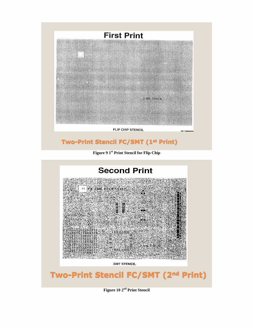
Assembly of flip Chip and Surface Mount Components on the same substrate may require a Two Print Stencil System. FC
attach may be achieved by placing the bumped die in a thin layer of flux, a thin layer of conductive polymer, or a thin layer of
solder paste. Normal thickness for these layers is 2 mils or less. The first print stencil prints this layer and the second print
stencil prints the SMD paste and has a relief pocket for the first print. This is illustrated in /figures 9 and 10. The second
print stencil normally has a relief pocket chemically etched into the stainless steel stencil foil and then has the apertures laser-
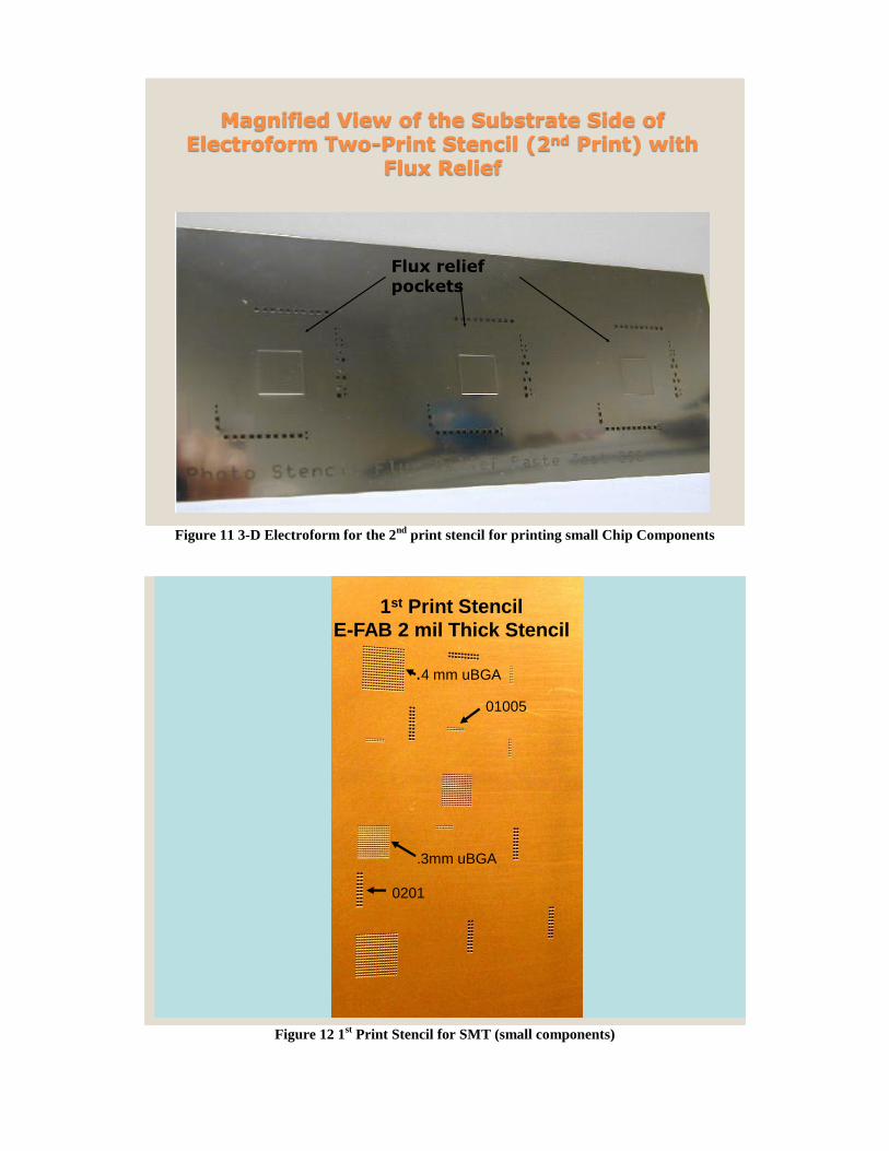
cut in the foil. It is also possible to construct a 3-D Electroform stencil for the second print stencil. In this case the relief
pocket is grown on a mandrel with the relief pocket machined into the surface of the mandrel. Such a stencil is shown in
Figure 11. There are a couple of requirements that drive the need to use this type of stencil. A relatively high relief pocket
can be formed in a thin stencil. A thin stencil ~ 2-3 mils thick may be required to print small chip components like 0201 and
01005 but the relief pocket may need to be 3-4 mils high for good clearance from the first print.
Printing Solder Paste for SMT and RF Shields
RF Shields may exhibit co-planarity problems. Normally additional solder paste height is required to compensate for this
problem. In small handheld devices other very small components are often positioned very close to the RF Shield. This
renders a normal step stencil impractical. The Two Print Stencil System is one possible solution for this application(3)
. The
1st print stencil is shown in Figure 12, a 2 mil thick Electroform stencil for the very small SMD’s. Figure 13 shows the 2
nd
print stencil for the RF Shield, a 7 mil thick stainless steel stencil with a 5 mil deep chem.-etched relief with laser-cut
apertures. Figure 15 shows solder paste deposits for the RF shield and the .3mm pitch uBGA.
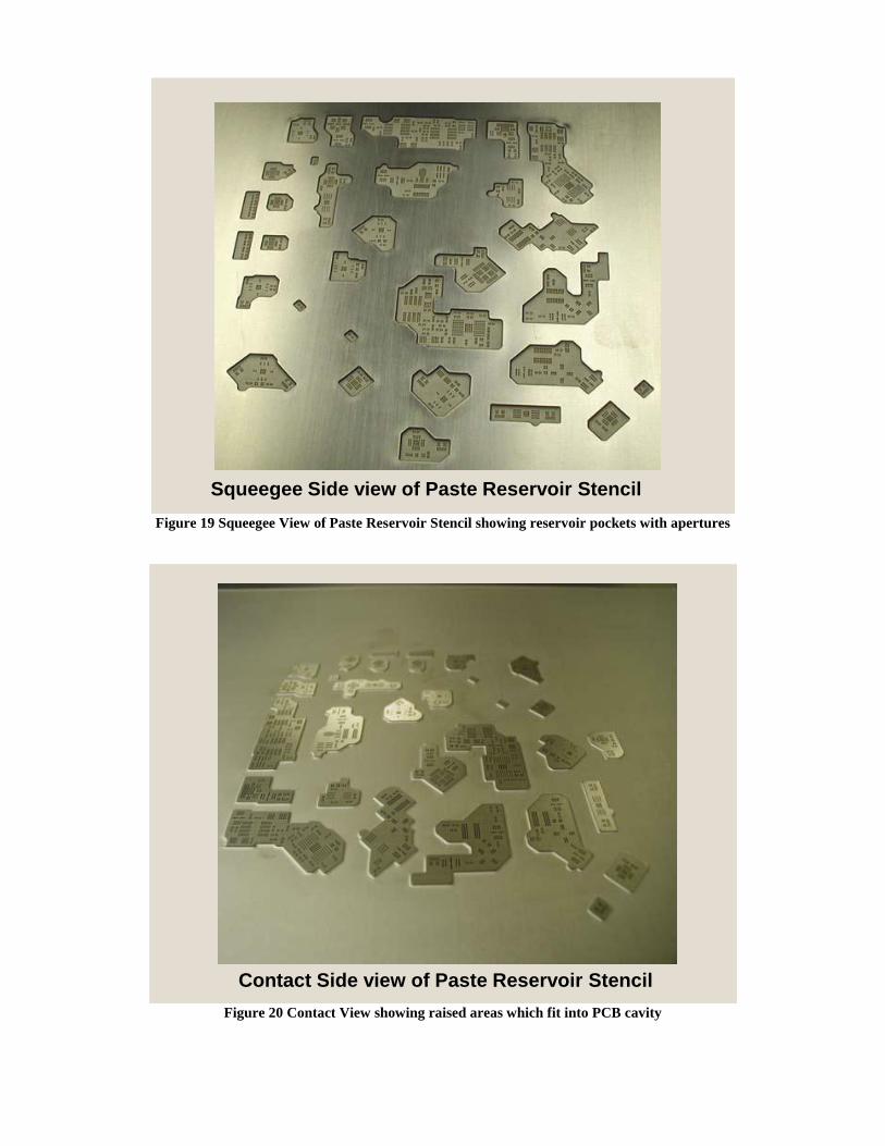
Printing Reservoir Solder Paste for multi-level boards
A recent design involved a circuit board with built in EMI shielding on one side and a laminated 20 mil thick ground plane
creating multiple recessed pockets of circuitry as shown in Figure 16. In the past, depositing solder paste on uneven surfaces
has been accomplished using dispensing methods. An alternative approach would be to use traditional printing methods as a
means for providing sufficient solder paste for reliable solder joints. In this case the surface mount pads are located in
multiple irregular shaped pockets 20 mils below the top surface. The stencil design(4)
is a 25 mil thick stencil with both
chem.-etch down and chem.-etch up pockets 20 mil thick leaving 5 mils of stencil over the recessed pads , which is shown in
Figure 17. Apertures the same size of the pads would lead to excessive solder deposits so circular apertures were staggered
over the pads, which are shown in Figure 18. The squeegee side view of the stencil is shown in figure 19 and the contact
(board side) view is shown in Figure 20. Reservoir Print results are seen in Figure 21.
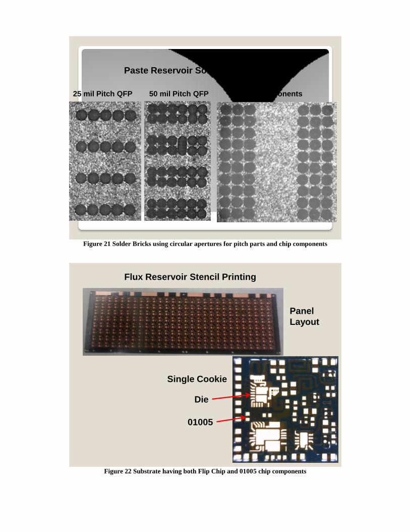
Printing Solder Paste and Reservoir Flux
The present application calls for assembly of FC as well as very small chip components, 0201 and 01005. Normally the
printing of flux for FC and paste for chip component and SMT devices could be accomplished by a normal two print stencil.
However in this case the paste stencil for 01005 requires a 2 mil thick stencil which leaves no room for a flux relief pocket on
the bottom side of the stencil. The Flux reservoir printing process is a two print stencil process but the printing sequences are
reversed(5)
. The “first stencil” is 2 mils thick and is used to print solder paste for the SMT and 01005 devices. The “second
stencil” is 8 mils thick with a 5 mil etch relief pocket on the contact side for clearance of the “first print” from the “first
stencil”. The reservoir pocket is etched down 6 mils leaving 2 mils thickness for the flux apertures. Figure 22 shows the
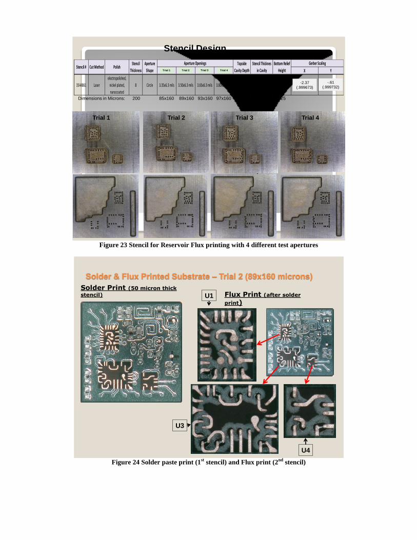
substrate with the FC pads and 0201 and 01005 chip capacitors. Figure 23 summarizes the stencil design showing both
squeegee and contact side views. Four different aperture designs (Trial 1 – Trial 4) were tested. Four different sets of
apertures were used: oblongs: 84 x 160 microns, 89 x 160 microns, 93 x 160 microns and 97 x 160 microns. Trial 2 gave
acceptable flux transfer as seen in Figure 23 which shows paste printed with the 1st print stencil and flux printed with the 2
nd
print stencil, note the paste bricks are unaffected by the 2nd
print.
Conclusions
The Two Print Stencil System has demonstrated an effective printing process for Surface Mount Assembly Including:
Through Hole / SMT Assembly
SMT / Flip Chip Assembly
FR Shield / SMT Assembly
SMT / Glue Chip Component Assembly
Multi-Level SMT Assembly
01005 / Die Attach Assembly
Other applications not mentioned in this paper including printing lead free and tin lead on the same PCB
1-“Lead Free Intrusive Reflow” W. Coleman and G. Oxx, APEX 2007

2- “Metal Stencils for Adhesive Printing”, W Coleman and A. Wadhwa, APEX 2002
3- “Stencil Options for Printing Solder Paste for .3mm pitch CSPs and 01005” Chip Components, W. Coleman and C.
Anglin, APEX 2010
4- “Reservoir Solder Paste Printing”. M. Burgess and J. Robbins, SMTAI 2007
5- Flux Reservoir stencil Printing”. W. Coleman and M. Read, SMTAI 2012
Alternative Header Layout and Paste Deposit
(Overprint) (60 mil annular ring)
Raw Card Wet Paste Deposit
36 mil ø40 mil ø44 mil ø48 mil ø 36 mil ø40 mil ø44 mil ø48 mil ø
Figure 1 Overprint for Through-Hole Device
X-Ray Picture of Axial Resistor Cross Sections after Reflow
.063” Board .093” Board
Overprint alone is sufficient to provide sufficient solder paste
Figure 2 X-Ray of Pin-In-Hole showing sufficient solder fill

Alternative Header Layout and Paste Deposit
(Overprint Constraints) (60 mil annular ring)
Raw Card Wet Paste Deposit
36 mil ø40 mil ø44 mil ø48 mil ø 36 mil ø40 mil ø44 mil ø48 mil ø
Figure 3 Print of 85 mil square paste bricks (100 mil pitch) for 2
nd Print Stencil
Two Print Stencil (typically 12-20 mils thick) for printing
solder paste for Intrusive Reflow of Through-Hole
components.
Relief pockets on bottom side for clearance of SMT solder
paste.
Figure 4 2
nd Print Stencil (Chem-Etch / Laser-Cut)

Lead Free Intrusive Reflow Test
Results for Alternating Header
View from non-squeegee side 63 mil thick PCB
Paste ON Header Pads and IN HeaderThrough Holes
Pins placed in theHeader ThroughHoles
Header Pins afterReflow
Paste Hole Fill is 100%
Figure 5 X –Ray view after print, after pin placement, after reflow
.063” Board/ .060” annular ring
(Header Cross Sections)
.036”
FHS
.040”
FHS
.044”
FHS
.048”
FHS
Header
Insufficient Solder Volume… Largest Hole Size (6mil stencil thickness)
Pin-Hole
Ratio .52 .56 .63 .69
Figure 6 Pin-In-Hole after reflow showing voiding for small Pin-Hole ratio’s

Two Print Stencil for printing Glue for Chip Components
after Solder paste. Stencil is 20 mils thick with a 15 mil
deep relief pocket
Figure 7 Printing Glue and Solder Paste for Chip Components
Picture showing Glue and Solder Paste for an 0805
Chip Component
Figure 8 Printed Paste (1
st stencil) and Glue (2
nd stencil)
Two-Print Stencil FC/SMT (1st Print)
Figure 9 1st Print Stencil for Flip Chip
Two-Print Stencil FC/SMT (2nd Print)
Figure 10 2
nd Print Stencil
Magnified View of the Substrate Side of Electroform Two-Print Stencil (2nd Print) with
Flux Relief
Flux relief pockets
Figure 11 3-D Electroform for the 2
nd print stencil for printing small Chip Components
1st Print Stencil
E-FAB 2 mil Thick Stencil
.4 mm uBGA
01005
.3mm uBGA
0201
Figure 12 1
st Print Stencil for SMT (small components)
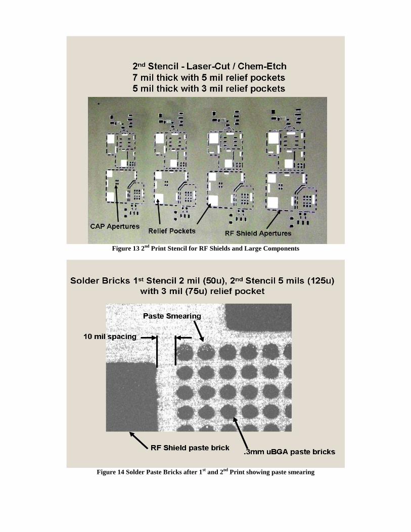
Figure 13 2
nd Print Stencil for RF Shields and Large Components
Figure 14 Solder Paste Bricks after 1
st and 2
nd Print showing paste smearing

Figure 15 Solder Paste Bricks after 1
st and 2
nd Print showing no paste smearing
Printing Reservoir Solder Paste
for multi-level boards
Component pads are recessed 12 mils below
top level of the board
Figure 16 Recessed Multi-Level Board

Figure 17 Stencil Design for Paste Reservoir Printing
Figure 18 Test Aperture Design to determine best paste coverage on the pads
Squeegee Side view of Paste Reservoir Stencil
Figure 19 Squeegee View of Paste Reservoir Stencil showing reservoir pockets with apertures
Contact Side view of Paste Reservoir Stencil
Figure 20 Contact View showing raised areas which fit into PCB cavity
Paste Reservoir Solder Bricks
25 mil Pitch QFP 50 mil Pitch QFP Chip Components
Figure 21 Solder Bricks using circular apertures for pitch parts and chip components
Flux Reservoir Stencil Printing
Panel
Layout
Single Cookie
Die
01005
Figure 22 Substrate having both Flip Chip and 01005 chip components
Stencil Design
Trial 1 Trial 2 Trial 3 Trial 4
Dimensions in Microns: 200 85x160 89x160 93x160 97x160 150 50 125
Cookie 1 Cookie 2 Cookie 3 Cookie 4 X Y
3544861 Laser
electropolished,
nickel plated,
nanocoated
8 Circle 3.35x6.3 mils 3.50x6.3 mils 3.65x6.3 mils 3.80x6.3 mils 6 mil 2 mil 5 mil ? ?
Aperture Openings Topside
Cavity Depth
Stencil Thicknes
in Cavity
Bottom Relief
Height
Gerber ScalingStencil # Cut Method Polish
Stencil
Thickness
Aperture
Shape Trial 1 Trial 2 Trial 3 Trial 4
-2.37
(.999673)
-.61
(.999732)
Figure 23 Stencil for Reservoir Flux printing with 4 different test apertures
Solder & Flux Printed Substrate – Trial 2 (89x160 microns)
Solder Print (50 micron thick
stencil) Flux Print (after solder
print)U1
U3
U4
Figure 24 Solder paste print (1st stencil) and Flux print (2
nd stencil)