two dimensional electron gas, quantum wells & semiconductor superlattices
TRANSCRIPT

Chapter 9
Two Dimensional Electron Gas,
Quantum Wells & Semiconductor
Superlattices
References:
• Ando, Fowler and Stern, Rev. Mod. Phys. 54 437 (1982).
• R.F. Pierret, Field Effect Devices, Vol. IV of Modular Series on Solid State Devices,Addison-Wesley (1983).
• B.G. Streetman, Solid State Electronic Devices, Series in Solid State Physical Elec-tronics, Prentice-Hall (1980).
9.1 Two-Dimensional Electronic Systems
One of the most important recent developments in semiconductors, both from the point ofview of physics and for the purpose of device developments, has been the achievement ofstructures in which the electronic behavior is essentially two-dimensional (2D). This meansthat, at least for some phases of operation of the device, the carriers are confined in apotential such that their motion in one direction is restricted and thus is quantized, leavingonly a two-dimensional momentum or k-vector which characterizes motion in a plane normalto the confining potential. The major systems where such 2D behavior has been studiedare MOS structures, quantum wells and superlattices. More recently, quantization has beenachieved in 1-dimension (the quantum wires) and “zero”–dimensions (the quantum dots).These topics are further discussed in Chapter 10 and in the course on semiconductor physics(6.735J).
9.2 MOSFETS
One of the most useful and versatile of these structures is the metal-insulator-semiconductor(MIS) layered structures, the most important of these being the metal-oxide-semiconductor
140
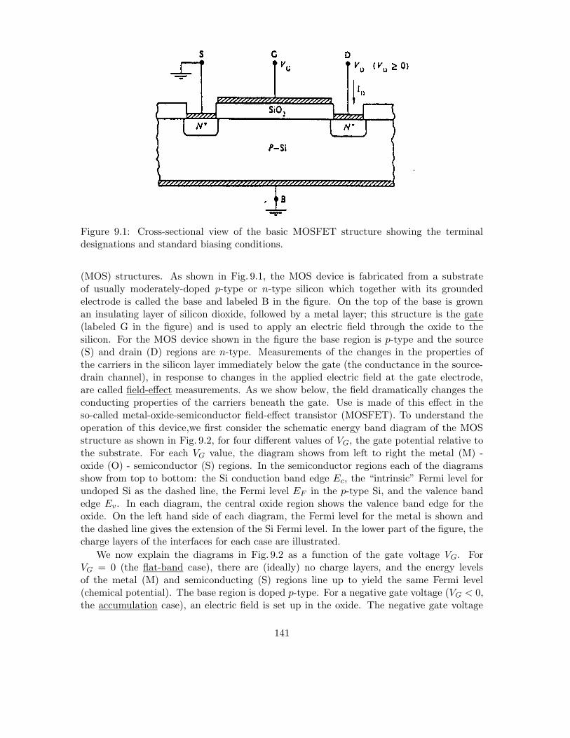
Figure 9.1: Cross-sectional view of the basic MOSFET structure showing the terminaldesignations and standard biasing conditions.
(MOS) structures. As shown in Fig. 9.1, the MOS device is fabricated from a substrateof usually moderately-doped p-type or n-type silicon which together with its groundedelectrode is called the base and labeled B in the figure. On the top of the base is grownan insulating layer of silicon dioxide, followed by a metal layer; this structure is the gate(labeled G in the figure) and is used to apply an electric field through the oxide to thesilicon. For the MOS device shown in the figure the base region is p-type and the source(S) and drain (D) regions are n-type. Measurements of the changes in the properties ofthe carriers in the silicon layer immediately below the gate (the conductance in the source-drain channel), in response to changes in the applied electric field at the gate electrode,are called field-effect measurements. As we show below, the field dramatically changes theconducting properties of the carriers beneath the gate. Use is made of this effect in theso-called metal-oxide-semiconductor field-effect transistor (MOSFET). To understand theoperation of this device,we first consider the schematic energy band diagram of the MOSstructure as shown in Fig. 9.2, for four different values of VG, the gate potential relative tothe substrate. For each VG value, the diagram shows from left to right the metal (M) -oxide (O) - semiconductor (S) regions. In the semiconductor regions each of the diagramsshow from top to bottom: the Si conduction band edge Ec, the “intrinsic” Fermi level forundoped Si as the dashed line, the Fermi level EF in the p-type Si, and the valence bandedge Ev. In each diagram, the central oxide region shows the valence band edge for theoxide. On the left hand side of each diagram, the Fermi level for the metal is shown andthe dashed line gives the extension of the Si Fermi level. In the lower part of the figure, thecharge layers of the interfaces for each case are illustrated.
We now explain the diagrams in Fig. 9.2 as a function of the gate voltage VG. ForVG = 0 (the flat-band case), there are (ideally) no charge layers, and the energy levelsof the metal (M) and semiconducting (S) regions line up to yield the same Fermi level(chemical potential). The base region is doped p-type. For a negative gate voltage (VG < 0,the accumulation case), an electric field is set up in the oxide. The negative gate voltage
141

Figure 9.2: Energy band and block charge diagrams for a p–type device under flat band,accumulation, depletion and inversion conditions.
causes the Si bands to bend up at the oxide interface (see Fig. 9.2) so that the Fermi levelis closer to the valence-band edge. Thus extra holes accumulate at the semiconductor-oxideinterface and electrons accumulate at the metal-oxide interface (see lower part of Fig. 9.2).In the third (depletion) case, the gate voltage is positive but less than some thresholdvalue VT . The voltage VT is defined as the gate voltage where the intrinsic Fermi leveland the actual Fermi level are coincident at the interface (see lower part of Fig. 9.2). Forthe “depletion” regime, the Si bands bend down at the interface resulting in a depletion ofholes, and a negatively charged layer of localized states is formed at the semiconductor-oxideinterface. The size of this “depletion region” increases as VG increases. The correspondingpositively charged region at the metal-oxide interface is also shown. Finally, for VG > VT ,the intrinsic Fermi level at the interface drops below the actual Fermi level, forming the“inversion layer”, where mobile electrons reside. It is the electrons in this inversion layerwhich are of interest, both because they can be confined so as to exhibit two-dimensionalbehavior, and because they can be controlled by the gate voltage in the MOSFET (seeFig. 9.3)
The operation of a metal-oxide semiconductor field-effect transistor (MOSFET) is illus-trated in Fig. 9.3, which shows the electron inversion layer under the gate for VG > VT (fora p-type substrate), with the source region grounded, for various values of the drain voltageVD. The inversion layer forms a conducting “channel” between the source and drain (aslong as VG > VT ). The dashed line in Fig. 9.3 shows the boundaries of the depletion regionwhich forms in the p-type substrate adjoining the n+ and p regions.
For VD = 0 there is obviously no current between the source and the drain since both areat the same potential. For VD > 0, the inversion layer or channel acts like a resistor, inducingthe flow of electric current ID. As shown in Fig. 9.3, increasing VD imposes a reverse biason the n+-p drain-substrate junction, thereby increasing the width of the depletion region
142

Figure 9.3: Visualization of various phases of VG > VT MOSFET operation. (a) VD = 0,(b) channel (inversion layer) narrowing under moderate VD biasing, (c) pinch–off, and (d)post-pinch-off (VD > VDsat) operation. (Note that the inversion layer widths, depletionwidths, etc. are not drawn to scale.)
143

Figure 9.4: General form of the ID − VD
characteristics expected from a long channel(∆L ¿ L) MOSFET.
and decreasing the number of carriers and narrowing the channel in the inversion layer asshown in Fig. 9.3. Finally as VD increases further, the channel reaches the “pinched-off”condition VDsat shown in Fig. 9.3c. Further increase in VD does not increase ID but rathercauses “saturation”. We note that at saturation, VDsat = VG − VT . Saturation is caused bya decrease in the carrier density in the channel due to the pinch-off phenomena.
In Fig. 9.4 ID vs. VD curves are plotted for fixed values of VG > VT . We note that VDsat
increases with increasing VG. These characteristic curves are qualitatively similar to thecurves for the bipolar junction transistor. The advantage of MOSFET devices lie in thespeed of their operation and in the ease with which they can be fabricated into ultra-smalldevices.
The MOSFET device, or an array of a large number of MOSFET devices, is fabricatedstarting with a large Si substrate or “wafer”. At each stage of fabrication, areas of thewafer which are to be protected are masked off using a light-sensitive substance calledphotoresist, which is applied as a thin film, exposed to light (or an electron or x-ray beam)through a mask of the desired pattern, then chemically developed to remove the photoresistfrom only the exposed (or, sometimes only the un–exposed) area. First the source anddrain regions are formed by either diffusing or implanting (bombarding) donor ions intothe p-type substrate. Then a layer of SiO2 (which is an excellent and stable insulator) isgrown by exposing the desired areas to an atmosphere containing oxygen; usually only athin layer is grown over the gate regions and, in a separate step, thicker oxide layers aregrown between neighboring devices to provide electrical isolation. Finally, the metal gateelectrode, the source and drain contacts are formed by sputtering or evaporating a metalsuch as aluminum onto the desired regions.
9.3 Two-Dimensional Behavior
Other systems where two-dimensional behavior has been observed include heterojunctionsof III-V compounds such as GaAs/Ga1−xAlxAs, layer compounds such as GaSe, GaSe2
and related III-VI compounds, graphite and intercalated graphite, and electrons on thesurface of liquid helium. The GaAs/Ga1−xAlxAs heterojunctions are important for device
144

applications because the lattice constants and the coefficient of expansion of GaAs andGa1−xAlxAs are very similar. This lattice matching permits the growth of high mobilitythin films of Ga1−xAlxAs on a GaAs substrate.
The interesting physical properties of the MOSFET lie in the two-dimensional behav-ior of the electrons in the channel inversion layer at low temperatures. Studies of theseelectrons have provided important tests of modern theories of localization, electron-electroninteractions and many-body effects. In addition, the MOSFETs have exhibited a highlyunexpected property that, in the presence of a magnetic field normal to the inversion layer,the transverse or Hall resistance ρxy is quantized in integer values of e2/h. This quantiza-tion is accurate to parts in 107 or 108 and provides the best measure to date of the finestructure constant α = e2/hc, when combined with the precisely-known velocity of light c.We will further discuss the quantized Hall effect later in the course (Part III).
We now discuss the two-dimensional behavior of the MOSFET devices in the absenceof a magnetic field. The two-dimensional behavior is associated with the nearly plane waveelectron states in the inversion layer. The potential V (z) is associated with the electric fieldV (z) = eEz and because of the negative charge on the electron, a potential well is formedcontaining bound states described by quantized levels. A similar situation occurs in thetwo–dimensional behavior for the case of electrons in quantum wells produced by molecularbeam epitaxy. Explicit solutions for the bound states in quantum wells are given in §9.4.We discuss in the present section the form of the differential equation and of the resultingeigenvalues and eigenfunctions.
A single electron in a one-dimensional potential well V (z) will, from elementary quantummechanics, have discrete allowed energy levels En corresponding to bound states and usuallya continuum of levels at higher energies corresponding to states which are not bound. Anelectron in a bulk semiconductor is in a three-dimensional periodic potential. In addition thepotential causing the inversion layer of a MOSFET or a quantum well in GaAs/Ga1−xAlxAscan be described by a one-dimensional confining potential V (z) and can be written usingthe effective-mass theorem
[E(−i~∇) + H′]Ψ = ih
(∂Ψ
∂t
)
(9.1)
where H′ = V (z). The energy eigenvalues near the band edge can be written as
E(~k) = E(~k0) +1
2
∑
i,j
(∂2E
∂ki∂kj
)
kikj (9.2)
so that the operator E(−i~∇) in Eq. 9.1 can be written as
E(−i~∇) =∑
i,j
pipj
2mi,j(9.3)
where the pi’s are the operators
pi =h
i
∂
∂xi(9.4)
which are substituted into Schrodinger’s equation. The effect of the periodic potential iscontained in the reciprocal of the effective mass tensor
1
mij=
1
h2
∂2E(~k)
∂ki∂kj
∣∣∣∣~k= ~k0
(9.5)
145

where the components of 1/mij are evaluated at the band edge at ~k0.If 1/mij is a diagonal matrix, the effective-mass equation HΨ = EΨ is solved by a
function of the formΨn,kx,ky = eikxxeikyyfn(z) (9.6)
where fn(z) is a solution of the equation
− h2
2mzz
d2fn
dz2+ V (z)fn = En,zfn (9.7)
and the total energy is
En(kx, ky) = En,z +h2
2mxxk2
x +h2
2myyk2
y. (9.8)
Since the En,z energies (n=0,1,2,...) are discrete, the energies states En(kx, ky) for each nvalue form a “sub-band”. We give below (in §9.3.1) a simple derivation for the discreteenergy levels by considering a particle in various potential wells (i.e., quantum wells). Theelectrons in these “sub–bands” form a 2D electron gas.
9.3.1 Quantum Wells and Superlattices
Many of the quantum wells and superlattices that are commonly studied today do notoccur in nature, but rather are deliberately structured materials (see Fig. 9.5). In the case ofsuperlattices formed by molecular beam epitaxy, the quantum wells result from the differentbandgaps of the two constituent materials. The additional periodicity is in one–dimension(1–D) which we take along the z–direction, and the electronic behavior is usually localizedon the basal planes (x–y planes) normal to the z–direction, giving rise to two–dimensionalbehavior.
A schematic representation of a semiconductor heterostructure superlattice is shown inFig. 9.5 where d is the superlattice periodicity composed of a distance d1, of semiconductorS1, and d2 of semiconductor S2. Because of the different band gaps in the two semiconduc-tors, potential wells and barriers are formed. For example in Fig. 9.5, the barrier heights inthe conduction and valence bands are ∆Ec and ∆Ev respectively. In Fig. 9.5 we see that thedifference in bandgaps between the two semiconductors gives rise to band offsets ∆Ec and∆Ev for the conduction and valence bands. In principle, these band offsets are determinedby matching the Fermi levels for the two semiconductors. In actual materials, the Fermilevels are highly sensitive to impurities, defects and charge transfer at the heterojunctioninterface.
The two semiconductors of a heterojunction superlattice could be different semiconduc-tors such as InAs with GaP (see Table 9.1 for parameters related to these compounds) or abinary semiconductor with a ternary alloy semiconductor, such as GaAs with AlxGa1−xAs(sometimes referred to by their slang names “Gaas” and “Algaas”). In the typical semicon-ductor superlattices the periodicity d = d1 + d2 is repeated many times (e.g., 100 times).The period thicknesses typically vary between a few layers and many layers (10A to 500A).Semiconductor superlattices are today an extremely active research field internationally.
The electronic states corresponding to the heterojunction superlattices are of two funda-mental types–bound states in quantum wells and nearly free electron states in zone–foldedenergy bands. In this course, we will limit our discussion to the bound states in a singleinfinite quantum well. Generalizations to multiple quantum wells will be made subsequently.
146

Figure 9.5: (a) A heterojunction superlattice of periodicity d. (b) Each superlattice unit cellconsists of a thickness d1 of material #1 and d2 of material #2. Because of the different bandgaps, a periodic array of potential wells and potential barriers is formed. When the bandoffsets are both positive as shown in this figure, the structure is called a type I superlattice.
Figure 9.6: The eigenfunctions and boundstate energies of an infinitely deep potentialwell used as an approximation to the statesin two finite wells. The upper well applies toelectrons and the lower one to holes. This dia-gram is a schematic representation of a quan-tum well in the GaAs region formed by the ad-jacent wider gap semiconductor AlxGa1−xAs.
147

Table 9.1: Material parameters of GaAs, GaP, InAs, and InP.1
Property Parameter (units) GaAs GaP InAs InP
Lattice constant a(A) 5.6533 5.4512 6.0584 5.8688Density g(g/cm3) 5.307 4.130 5.667 4.787Thermal expansion αth(×10−6/C) 6.63 5.91 5.16 4.56Γ point band gap E0(eV) 1.42 2.74 0.36 1.35
plus spin orbit E0 + ∆0(eV) 1.76 2.84 0.79 1.45L point band gap E1(eV) 2.925 3.75 2.50 3.155
plus spin orbit E1 + ∆1(eV) 3.155 . . . 2.78 3.305Γ point band gap E0
′(eV) 4.44 4.78 4.44 4.72∆ axis band gap E2(eV) 4.99 5.27 4.70 5.04
plus spin orbit E2 + δ(eV) 5.33 5.74 5.18 5.60Gap pressure coefficient ∂E0/∂P (×10−6eV/bar) 11.5 11.0 10.0 8.5Gap temperature coefficient ∂E0/∂T (×10−4eV/C) −3.95 −4.6 −3.5 −2.9Electron mass m∗/m0 0.067 0.17 0.023 0.08
light hole m`h∗/m0 0.074 0.14 0.027 0.089
heavy hole mhh∗/m0 0.62 0.79 0.60 0.85
spin orbit hole mso∗/m0 0.15 0.24 0.089 0.17
Dielectric constant: static εs 13.1 11.1 14.6 12.4Dielectric constant: optic ε∞ 11.1 8.46 12.25 9.55Ionicity f1 0.310 0.327 0.357 0.421Polaron coupling αF 0.07 0.20 0.05 0.08Elastic constants c11(×1011dyn/cm2) 11.88 14.120 8.329 10.22
c12(×1011dyn/cm2) 5.38 6.253 4.526 5.76c44(×1011dyn/cm2) 5.94 7.047 3.959 4.60
Young’s modulus Y (×1011dyn/cm2) 8.53 10.28 5.14 6.07P 0.312 0.307 0.352 0.360
Bulk modulus B(×1011 dyn/cm2) 7.55 8.88 5.79 7.25A 0.547 0.558 0.480 0.485
Piezo–electric coupling e14(C/m2) −0.16 −0.10 −0.045 −0.035K[110] 0.0617 0.0384 0.0201 0.0158
Deformation potential a(eV) 2.7 3.0 2.5 2.9b(eV) −1.7 −1.5 −1.8 −2.0d(eV) −4.55 −4.6 −3.6 −5.0
Deformation potential Ξeff (eV) 6.74 6.10 6.76 7.95Donor binding G(meV) 4.4 10.0 1.2 5.5Donor radius aB(A) 136 48 406 106Thermal conductivity κ(watt/deg − cm) 0.46 0.77 0.273 0.68Electron mobility µn(cm2/V − sec) 8000 120 30000 4500Hole mobility µp(cm
2/V − sec) 300 – 450 100
1Table from J. Appl. Physics 53, 8777 (1982).
148

9.4 Bound Electronic States
From the diagram in Fig. 9.5 we see that the heterojunction superlattice consists of anarray of potential wells. The interesting limit to consider is the case where the width of thepotential well contains only a small number of crystallographic unit cells (Lz < 100 A), inwhich case the number of bound states in the well is a small number.
From a mathematical standpoint, the simplest case to consider is an infinitely deeprectangular potential well. In this case, a particle of mass m∗ in a well of width Lz in thez direction satisfies the free particle Schrodinger equation
− h2
2m∗d2ψ
dz2= Eψ (9.9)
with eigenvalues
En =h2
2m∗
(nπ
Lz
)2
=
(h2π2
2m∗L2z
)
n2 (9.10)
and the eigenfunctions
ψn = A sin(nπz/Lz) (9.11)
where n = 1,2,3.... are the plane wave solutions that satisfy the boundary conditions thatthe wave functions in Eq. 9.11 must vanish at the walls of the quantum wells (z = 0 andz = Lz).
We note that the energy levels are not equally spaced, but have energies En ∼ n2, thoughthe spacings En+1 −En are proportional to n. We also note that En ∼ Lz
−2, so that as Lz
becomes large, the levels become very closely spaced as expected for a 3D semiconductor.However when Lz decreases, the number of states in the quantum well decreases, so thatfor a well depth Ed it would seem that there is a critical width Lz
c below which there wouldbe no bound states
Lzc =
hπ
(2m∗Ed)1
2
. (9.12)
An estimate for Lzc is obtained by taking m∗ = 0.1m0 and Ed = 0.1 eV to yield Lz
c = 61A.There is actually a theorem in quantum mechanics that says that there will be at leastone bound state for an arbitrarily small potential well. More exact calculations consideringquantum wells of finite thickness have been carried out, and show that the infinite wellapproximation gives qualitatively correct results.
The closer level spacing of the valence band bound states in Fig. 9.6 reflects the heav-ier masses in the valence band. Since the states in the potential well are quantized, thestructures in Figs. 9.5 and 9.6 are called quantum well structures.
If the potential energy of the well V0 is not infinite but finite, the wave functions aresimilar to those given in Eq. 9.11, but will have decaying exponentials on either side of thepotential well walls. The effect of the finite size of the well on the energy levels and wavefunctions is most pronounced near the top of the well. When the particle has an energygreater than V0, its eigenfunction corresponds to a continuum state exp(ikzz).
In the case of MOSFETs, the quantum well is not of rectangular shape as shown inFig. 9.7, but rather is approximated as a triangular well. The solution for the bound statesin a triangular well cannot be solved exactly, but can only be done approximately, as forexample using the WKB approximation described in §9.6.
149

Figure 9.7: Schematic of a potential barrier.
E
V0
#1 #2 #3
Lz
V = 00
9.5 Review of Tunneling Through a Potential Barrier
When the potential well is finite, the wave functions do not completely vanish at the wallsof the well, so that tunneling through the potential well becomes possible. We now brieflyreview the quantum mechanics of tunneling through a potential barrier. We will return totunneling in semiconductor heterostructures after some introductory material.
Suppose that the potential V shown in Fig. 9.7 is zero (V = 0) in regions #1 and #3,while V = V0 in region #2. Then in regions #1 and #3
E =h2k2
2m∗ (9.13)
ψ = eikz (9.14)
while in region #2 the wave function is exponentially decaying
ψ = ψ0e−βz (9.15)
so that substitution into Schrodinger’s equation gives
−h2
2m∗β2ψ + (V0 − E)ψ = 0 (9.16)
or
β2 =2m∗
h2 (V0 − E). (9.17)
The probability that the electron tunnels through the rectangular potential barrier is thengiven by
P = exp
− 2
∫ Lz
0β(z)dz
= exp
− 2
(2m∗
h2
) 1
2
(V0 − E)1
2 Lz
(9.18)
As Lz increases, the probability of tunneling decreases exponentially. Electron tunnelingphenomena frequently occur in solid state physics.
9.6 Quantum Wells of Different Shape and the WKB Ap-
proximation
With the sophisticated computer control available with state of the art molecular beam epi-taxy systems it is now possible to produce quantum wells with specified potential profilesV (z) for semiconductor heterojunction superlattices. Potential wells with non–rectangular
150

Figure 9.8: Schematic of a rectangular well.
−V0
E
#1 #2 #3
a−a
profiles also occur in the fabrication of other types of superlattices (e.g., by modulation dop-ing). We therefore briefly discuss (in the recitation class) bound states in general potentialwells.
In the general case where the potential well has an arbitrary shape, solution by the WKB(Wentzel–Kramers–Brillouin) approximation is very useful (see for example, Shanker, “Prin-ciples of Quantum Mechanics”, Plenum press, chapter 6). According to this approximation,the energy levels satisfy the Bohr–Sommerfeld quantization condition
∫ z2
z1
pzdz = hπ(r + c1 + c2) (9.19)
where pz = (2m∗[E − V ])1
2 and the quantum number r is an integer r = 0, 1, 2, . . . while c1
and c2 are the phases which depend on the form of V (z) at the turning points z1 and z2
where V (zi) = E. If the potential has a sharp discontinuity at a turning point, then c =1/2, but if V depends linearly on z at the turning point then c = 1/4.
For example for the infinite rectangular well (see Fig. 9.8)
V (z) = 0 for | z |< a (inside the well) (9.20)
V (z) = ∞ for | z |> a (outside the well) (9.21)
By the WKB rules, the turning points occur at the edges of the rectangular well and
therefore c1 = c2 = 1/2. In this case pz is a constant, independent of z so that pz = (2m∗E)1
2
and Eq. 9.19 yields
(2m∗E)1
2 Lz = hπ(r + 1) = hπn (9.22)
where n = r + 1 and
En =h2π2
2m∗Lz2 n2 (9.23)
in agreement with the exact solution given by Eq. 9.10. The finite rectangular well shownin Fig. 9.8 is thus approximated as an infinite well with solutions given by Eq. 9.10.
As a second example consider a harmonic oscillator potential well shown in Fig. 9.9,where V (z) = m∗ω2z2/2. The harmonic oscillator potential well is typical of quantumwells in periodically doped (nipi which is n-type; insulator; p-type; insulator) superlattices.In this case
pz = (2m∗)1/2(
E − m∗ω2
2z2
) 1
2
. (9.24)
The turning points occur when V (z) = E so that the turning points are given by z =
±(2E/m∗ω2)1
2 . Near the turning points V (z) is approximately linear in z, so the phase
151

Figure 9.9: Schematic of a harmonic oscillator well.
Figure 9.10: Schematic of a triangular well.
¡¡
¡¡
¡
E
−V0
#1 #2 #3
a−a
factors become c1 = c2 = 14 . The Bohr–Sommerfeld quantization thus yields
∫ z2
z1
pzdz =
∫ z2
z1
(2m∗)1
2
(
E − m∗ω2
2z2
) 1
2
dz = hπ(r +1
2). (9.25)
Making use of the integral relation
∫√
a2 − u2 du =u
2
√
a2 − u2 +a2
2sin−1 u
a(9.26)
we obtain upon substitution of Eq. 9.26 into 9.25:
(2m∗)1
2
(
m∗ω2
2
) 1
2(
Er
m∗ω2
)
π =Erπ
ω= hπ(r +
1
2) (9.27)
which simplifies to the familiar relation for the harmonic oscillator energy levels:
Er = hω(r +1
2) where r = 0, 1, 2... (9.28)
another example of an exact solution. For homework, you will use the WKB method to findthe energy levels for an asymmetric triangular well. Such quantum wells are typical of theinterface of metal–insulator–semiconductor (MOSFET) device structures (see Fig. 9.10).
9.7 The Kronig–Penney Model
We review here the Kronig–Penney model which gives an explicit solution for a one–dimensional array of finite potential wells shown in Fig. 9.11. Starting with the one di-mensional Hamiltonian with a periodic potential (see Eq. 9.7)
− h2
2m∗d2ψ
dz2+ V (z)ψ = Eψ (9.29)
152

Figure 9.11: Kronig–Penney square well periodic potential
we obtain solutions in the region 0 < z < a where V (z) = 0
ψ(z) = AeiKz + Be−iKz (9.30)
E =h2K2
2m∗ (9.31)
and in the region −b < z < 0 where V (z) = V0 (the barrier region)
ψ(z) = Ceβz + De−βz (9.32)
where
β2 =2m∗
h2 [V0 − E]. (9.33)
Continuity of ψ(z) and dψ(z)/dz at z = 0 and z = a determines the coefficients A, B, C, D.At z = 0 we have:
A + B=C + D
iK(A − B)=β(C − D)
(9.34)
At z = a, we apply Bloch’s theorem (see Fig. 9.11), introducing a factor exp[ik(a + b)] toobtain ψ(a) = ψ(−b) exp[ik(a + b)]
AeiKa + Be−iKa=(Ce−βb + Deβb)eik(a+b)
iK(AeiKa − Be−iKa)=β(Ce−βb − Deβb)eik(a+b).
(9.35)
These 4 equations (Eqs. 9.34 and 9.35) in 4 unknowns determine A, B, C, D. The vanishingof the coefficient determinant restricts the conditions under which solutions to the Kronig–Penney model are possible, leading to the algebraic equation
β2 − K2
2βKsinh βb sin Ka + cosh βb cos Ka = cos k(a + b) (9.36)
which has solutions for a limited range of β values.
153

Figure 9.12: Plot of energy vs. k for theKronig–Penney model with P = 3π/2. (Af-ter Sommerfeld and Bethe.)
Normally the Kronig–Penney model in the textbooks is solved in the limit b → 0 andV0 → ∞ in such a way that [β2ba/2] = P remains finite. The restricted solutions in thislimit lead to the energy bands shown in Fig. 9.12.
For the superlattice problem we are interested in solutions both within the quantum wellsand in the continuum. This is one reason for discussing the Kronig–Penny model. Anotherreason for discussing this model is because it provides a review of boundary conditions andthe application of Bloch’s theorem. In the quantum wells, the permitted solutions giverise to narrow bands with large band gaps while in the continuum regions the solutionscorrespond to wide bands and small band gaps.
9.8 3D Motion within a 1–D Rectangular Well
The thin films used for the fabrication of quantum well structures (see §9.4) are very thinin the z–direction but have macroscopic size in the perpendicular x–y plane. An exampleof a quantum well structure would be a thin layer of GaAs sandwiched between two thickerAlxGa1−xAs layers, as shown in the Fig. 9.5. For the thin film, the motion in the x andy directions is similar to that of the corresponding bulk solid which can be treated by theconventional 1–electron approximation and the Effective Mass Theorem. Thus the potentialcan be written as a sum of a periodic term V (x, y) and the quantum well term V (z). Theelectron energies thus are superimposed on the quantum well energies, the periodic solutionsobtained from solution of the 2–D periodic potential
En(kx, ky) = En,z +h2(k2
x + k2y)
2m∗ = En,z + E⊥ (9.37)
154
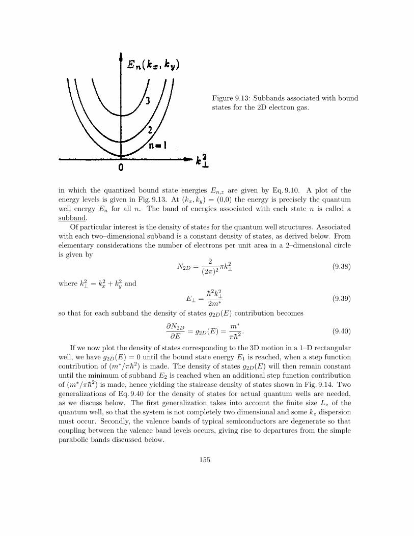
Figure 9.13: Subbands associated with boundstates for the 2D electron gas.
in which the quantized bound state energies En,z are given by Eq. 9.10. A plot of theenergy levels is given in Fig. 9.13. At (kx, ky) = (0,0) the energy is precisely the quantumwell energy En for all n. The band of energies associated with each state n is called asubband.
Of particular interest is the density of states for the quantum well structures. Associatedwith each two–dimensional subband is a constant density of states, as derived below. Fromelementary considerations the number of electrons per unit area in a 2–dimensional circleis given by
N2D =2
(2π)2πk2
⊥ (9.38)
where k2⊥ = k2
x + k2y and
E⊥ =h2k2
⊥2m∗ (9.39)
so that for each subband the density of states g2D(E) contribution becomes
∂N2D
∂E= g2D(E) =
m∗
πh2 . (9.40)
If we now plot the density of states corresponding to the 3D motion in a 1–D rectangularwell, we have g2D(E) = 0 until the bound state energy E1 is reached, when a step functioncontribution of (m∗/πh2) is made. The density of states g2D(E) will then remain constantuntil the minimum of subband E2 is reached when an additional step function contributionof (m∗/πh2) is made, hence yielding the staircase density of states shown in Fig. 9.14. Twogeneralizations of Eq. 9.40 for the density of states for actual quantum wells are needed,as we discuss below. The first generalization takes into account the finite size Lz of thequantum well, so that the system is not completely two dimensional and some kz dispersionmust occur. Secondly, the valence bands of typical semiconductors are degenerate so thatcoupling between the valence band levels occurs, giving rise to departures from the simpleparabolic bands discussed below.
155
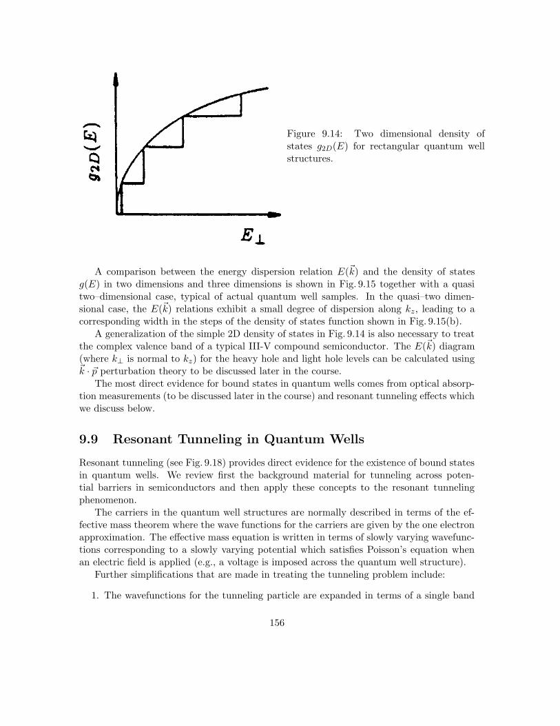
Figure 9.14: Two dimensional density ofstates g2D(E) for rectangular quantum wellstructures.
A comparison between the energy dispersion relation E(~k) and the density of statesg(E) in two dimensions and three dimensions is shown in Fig. 9.15 together with a quasitwo–dimensional case, typical of actual quantum well samples. In the quasi–two dimen-sional case, the E(~k) relations exhibit a small degree of dispersion along kz, leading to acorresponding width in the steps of the density of states function shown in Fig. 9.15(b).
A generalization of the simple 2D density of states in Fig. 9.14 is also necessary to treatthe complex valence band of a typical III-V compound semiconductor. The E(~k) diagram(where k⊥ is normal to kz) for the heavy hole and light hole levels can be calculated using~k · ~p perturbation theory to be discussed later in the course.
The most direct evidence for bound states in quantum wells comes from optical absorp-tion measurements (to be discussed later in the course) and resonant tunneling effects whichwe discuss below.
9.9 Resonant Tunneling in Quantum Wells
Resonant tunneling (see Fig. 9.18) provides direct evidence for the existence of bound statesin quantum wells. We review first the background material for tunneling across poten-tial barriers in semiconductors and then apply these concepts to the resonant tunnelingphenomenon.
The carriers in the quantum well structures are normally described in terms of the ef-fective mass theorem where the wave functions for the carriers are given by the one electronapproximation. The effective mass equation is written in terms of slowly varying wavefunc-tions corresponding to a slowly varying potential which satisfies Poisson’s equation whenan electric field is applied (e.g., a voltage is imposed across the quantum well structure).
Further simplifications that are made in treating the tunneling problem include:
1. The wavefunctions for the tunneling particle are expanded in terms of a single band
156
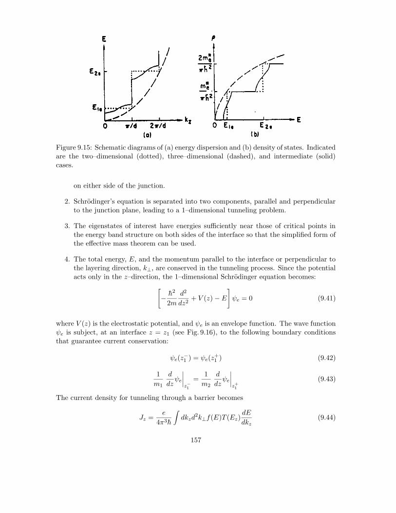
Figure 9.15: Schematic diagrams of (a) energy dispersion and (b) density of states. Indicatedare the two–dimensional (dotted), three–dimensional (dashed), and intermediate (solid)cases.
on either side of the junction.
2. Schrodinger’s equation is separated into two components, parallel and perpendicularto the junction plane, leading to a 1–dimensional tunneling problem.
3. The eigenstates of interest have energies sufficiently near those of critical points inthe energy band structure on both sides of the interface so that the simplified form ofthe effective mass theorem can be used.
4. The total energy, E, and the momentum parallel to the interface or perpendicular tothe layering direction, k⊥, are conserved in the tunneling process. Since the potentialacts only in the z–direction, the 1–dimensional Schrodinger equation becomes:
[
− h2
2m
d2
dz2+ V (z) − E
]
ψe = 0 (9.41)
where V (z) is the electrostatic potential, and ψe is an envelope function. The wave functionψe is subject, at an interface z = z1 (see Fig. 9.16), to the following boundary conditionsthat guarantee current conservation:
ψe(z−1 ) = ψe(z
+1 ) (9.42)
1
m1
d
dzψe
∣∣∣∣z−1
=1
m2
d
dzψe
∣∣∣∣z+1
(9.43)
The current density for tunneling through a barrier becomes
Jz =e
4π3h
∫
dkzd2k⊥f(E)T (Ez)
dE
dkz(9.44)
157

Figure 9.16: Rectangular–potential model (a) used to describe the effect of an insulator, 2,between two metals, 1 and 3. When a negative bias is applied to 1, electrons, with energiesup to the Fermi energy EF , can tunnel through the barrier. For small voltages, (b), thebarrier becomes trapezoidal, but at high bias (c), it becomes triangular.
where f(E) is the Fermi–Dirac distribution, and T (Ez) is the probability of tunnelingthrough the potential barrier. Here T (Ez) is expressed as the ratio between the transmittedand incident probability currents.
If an external bias V is applied to the barrier (see Fig. 9.16), the net current flowingthrough it is the difference between the current from left to right and that from right toleft. Thus, we obtain:
Jz =e
4π3h
∫
dEzd2k⊥[f(E) − f(E + eV )]T (Ez) (9.45)
where Ez represents the energy from the kz component of crystal momentum, i.e., Ez =h2k2
z/(2m). Since the integrand is not a function of k⊥ in a plane normal to kz, we canintegrate over d2k⊥ by writing
dkxdky = d2k⊥ =2m
h2 dE⊥ (9.46)
where E⊥ = h2k2⊥/(2m) and after some algebra, the tunneling current can be written as,
Jz=em
2π2h3
[
eV∫ EF−eV0 dEzT (Ez) +
∫ EFEF−eV dEz(EF − Ez)T (Ez)
]
if eV ≤ EF
Jz=em
2π2h3
∫ EF0 dEz(EF − Ez)T (Ez) if eV ≥ EF
(9.47)
(see Fig. 9.16 for the geometry of the model) which can be evaluated as long as the tun-neling probability through the barrier is known. We now discuss how to find the tunnelingprobability.
An enhanced tunneling probability occurs for certain voltages as a consequence of theconstructive interference between the incident and the reflected waves in the barrier regionbetween regions 1 and 3. To produce an interference effect the wavevector ~k in the plane
158

Figure 9.17: (a) Tunneling current through a rectangular barrier (like the one of Fig. 9.16a)calculated as a function of bias for different values of m1, in the quantum well. (b) Compar-ison of an exact calculation of the tunneling probability through a potential barrier underan external bias with an approximate result obtained using the WKB method. The barrierparameters are the same as in (a), and the energy of an incident electron, of mass 0.2m0,is 0.05eV. (From the book of E.E. Mendez and K. von Klitzing, “Physics and Applicationsof Quantum Wells and Superlattices”, NATO ASI Series, Vol. 170, p.159 (1987)).
wave solution eikz must have a real component so that an oscillating (rather than a decayingexponential) solution is possible. To accomplish this, it is necessary for a sufficiently highelectric field to be applied (as in Fig. 9.16(c)) so that a virtual bound state is formed. Ascan be seen in Fig. 9.17a, the oscillations are most pronounced when the difference betweenthe electronic mass at the barrier and at the electrodes is the largest. This interference phe-nomenon is frequently called resonant Fowler–Nordheim tunneling and has been observedin metal–oxide–semiconductor (MOS) heterostructures and in GaAs/Ga1−xAlxAs/GaAscapacitors. Since the WKB method is semiclassical, it does not give rise to the resonanttunneling phenomenon, which is a quantum interference effect.
For the calculation of the resonant tunneling phenomenon, we must therefore use thequantum mechanical solution. In this case, it is convenient to use the transfer–matrixmethod to find the tunneling probability. In region (#1) of Fig. 9.16, the potential V (z) isconstant and solutions to Eq. 9.41 have the form
ψe(z) = A exp(ikz) + B exp(−ikz) (9.48)
withh2k2
2m= E − V. (9.49)
159

When E −V > 0, then k is real and the wave functions are plane waves. When E −V < 0,then k is imaginary and the wave functions are growing or decaying waves. The boundaryconditions Eqs. 9.42 and 9.43 determine the coefficients A and B which can be described bya (2 × 2) matrix R such that
(
A1
B1
)
= R
(
A2
B2
)
(9.50)
where the subscripts on A and B refer to the region index and R can be written as
R =1
2k1m2
(k1m2 + k2m1) exp[i(k2 − k1)z1] (k1m2 − k2m1) exp[−i(k2 + k1)z1]
(k1m2 − k2m1) exp[i(k2 + k1)z1] (k1m2 + k2m1) exp[−i(k2 − k1)z1]
(9.51)and the terms in R of Eq. 9.51 are obtained by matching boundary conditions as given inEqs. 9.42 and 9.43.
In general, if the potential profile consists of n regions, characterized by the potentialvalues Vi and the masses mi (i = 1, 2, . . . n), separated by n − 1 interfaces at positions zi
(i = 1, 2, . . . (n − 1)), then
(
A1
B1
)
= (R1R2 . . . Rn−1)
(
An
Bn
)
. (9.52)
The matrix elements of Ri are
(Ri)1,1=(
12 + ki+1mi
2kimi+1
)
exp[i(ki+1 − ki)zi]
(Ri)1,2=(
12 − ki+1mi
2kimi+1
)
exp[−i(ki+1 + ki)zi]
(Ri)2,1=(
12 − ki+1mi
2kimi+1
)
exp[i(ki+1 + ki)zi]
(Ri)2,2=(
12 + ki+1mi
2kimi+1
)
exp[−i(ki+1 − ki)zi]
(9.53)
where the ki are defined by Eq. 9.49. If an electron is incident from the left (region #1)only a transmitted wave will appear in the last region #n, and therefore Bn = 0. Thetransmission probability is then given by
T =
(k1mn
knm1
) |An|2|A1|2
. (9.54)
This is a general solution to the problem of transmission through multiple barriers. Undercertain conditions, a particle incident on the left can appear on the right essentially withoutattenuation. This situation, called resonant tunneling, corresponds to a constructive inter-ference between the two plane waves coexisting in the region between the barriers (quantumwell).
The tunneling probability through a double rectangular barrier is illustrated in Fig. 9.18.In this figure, the mass of the particle is taken to be 0.067m0, the height of the barriers is0.3eV, their widths are 50A and their separations are 60A. As observed in the figures, forcertain energies below the barrier height, the particle can tunnel without attenuation. These
160

Figure 9.18: (a) Probability of tunneling through a double rectangular barrier as a functionof energy. The carrier mass is taken to be 0.1m0 in the barrier and 0.067m0 outside, andthe width of the quantum well is 60A. (b) Tunneling probability through a double–barrierstructure, subject to an electric field of 1 × 10⁵V/cm. The width of the left barrier is 50A,while that of the right barrier is varied between 50A and 100A. The peak at ∼ 0.16eVcorresponds to resonant tunneling through the first excited state (E1) of the quantum well.The optimum transmission is obtained when the width of the right barrier is ∼ 75A.
161

energies correspond precisely to the eigenvalues of the quantum well; this is understandable,since the solutions of Schrodinger’s equation for an isolated well are standing waves. Whenthe widths of the two barriers are different (see Fig. 9.18b), the tunneling probability doesnot reach unity, although the tunneling probability shows maxima for incident energiescorresponding to the bound and virtual states.
162

Chapter 10
Transport in Low Dimensional
Systems
References:
• Solid State Physics, Volume 44, Semiconductor Heterostructures and Nanostructures.Edited by H. Ehrenreich and D. Turnbull, Academic Press (1991).
• Electronic transport in mesoscopic systems, Supriyo Datta, Cambridge UniversityPress, 1995.
10.1 Introduction
Transport phenomena in low dimensional systems such as in quantum wells (2D), quantumwires (1D), and quantum dots (0D) are dominated by quantum effects not included inthe classical treatments based on the Boltzmann equation and discussed in Chapters 4-6.With the availability of experimental techniques to synthesize materials of high chemicalpurity and of nanometer dimensions, transport in low dimensional systems has become anactive current research area. In this chapter we consider some highlights on the subject oftransport in low dimensional systems.
10.2 Observation of Quantum Effects in Reduced Dimen-
sions
Quantum effects dominate the transport in quantum wells and other low dimensional sys-tems such as quantum wires and quantum dots when the de Broglie wavelength of theelectron
λdB =h
(2m∗E)1/2(10.1)
exceeds the dimensions of a quantum structure of characteristic length Lz (λdB > Lz)or likewise for tunneling through a potential barrier of length Lz. To get some order ofmagnitude estimates of the electron kinetic energies E below which quantum effects becomeimportant we look at Fig. 10.1 where a log-log plot of λdB vs E in Eq. 10.1 is shown for
163

Figure 10.1: Plot of the electron de Broglie wavelength λdB vs the electron kinetic energyE for GaAs (2) and InAs (¦).
164

GaAs and InAs. From the plot we see that an electron energy of E ∼ 0.1 eV for GaAscorresponds to a de Broglie wavelength of 200 A. Thus wave properties for electrons can beexpected for structures smaller than λdB.
To observe quantum effects, the thermal energy must also be less than the energy levelseparation, kBT < ∆E, where we note that room temperature corresponds to 25 meV. Sincequantum effects depend on the phase coherence of electrons, scattering can also destroyquantum effects. The observation of quantum effects thus requires that the carrier meanfree path be much larger than the dimensions of the quantum structures (wells, wires ordots).
The limit where quantum effects become important has been given the name of meso-
scopic physics. Carrier transport in this limit exhibits both particle and wave character-istics. In this ballistic transport limit, carriers can in some cases transmit charge or energywithout scattering.
The small dimensions required for the observation of quantum effects can be achievedby the direct fabrication of semiconductor elements of small dimensions (quantum wells,quantum wires and quantum dots). Another approach is the use of gates on a field effecttransistor to define an electron gas of reduced dimensionality. In this context, negativelycharged metal gates can be used to control the source to drain current of a 2D electrongas formed near the GaAs/AlGaAs interface as shown in Fig. 10.2. Between the dual gatesshown on this figure, a thin conducting wire is formed out of the 2D electron gas. Controllingthe gate voltage controls the amount of charge in the depletion region under the gates, aswell as the charge in the quantum wire. Thus lower dimensional channels can be made ina 2D electron gas by using metallic gates. In the following sections a number of importantapplications are made of this concept.
10.3 Density of States in Low Dimensional Systems
We showed in Eq. 8.40 that the density of states for a 2D electron gas is a constant for each2D subband
g2D =m∗
πh2 . (10.2)
This is shown in Fig. 10.3(a) where the inset is appropriate to the quantum well formednear a modulation doped GaAs-AlGaAs interface. In the diagram only the lowest boundstate is occupied.
Using the same argument, we now derive the density of states for a 1D electron gas
N1D =2
2π(k) =
1
π(k) (10.3)
which for a parabolic band E = En + h2k2/(2m∗) becomes
N1D =2
2π(k) =
1
π
(2m∗(E − En)
h2
)1/2
(10.4)
yielding an expression for the density of states g1D(E) = ∂N1D/∂E
g1D(E) =1
2π
(2m∗
h2
)1/2
(E − En)−1/2. (10.5)
165

Figure 10.2: (a) Schematic diagram of a lateral resonant tunneling field-effect transistorwhich has two closely spaced fine finger metal gates; (b) schematic of an energy banddiagram for the device. A 1D quantum wire is formed in the 2D electron gas between thegates.
166

Figure 10.3: Density of states g(E) as a function of energy. (a) Quasi-2D density of states,with only the lowest subband occupied (hatched). Inset: Confinement potential perpendic-ular to the plane of the 2DEG. The discrete energy levels correspond to the bottoms of thefirst and second 2D subbands. (b) Quasi-1D density of states, with four 1D subbands occu-pied. Inset: Square-well lateral confinement potential with discrete energy levels indicatingthe 1D subband extrema.
The interpretation of this expression is that at each doubly confined bound state level En
there is a singularity in the density of states, as shown in Fig. 10.3(b) where the first fourlevels are occupied.
10.3.1 Quantum Dots
This is an example of a zero dimensional system. Since the levels are all discrete anyaveraging would involve a sum over levels and not an integral over energy. If, however, onechooses to think in terms of a density of states, then the DOS would be a delta functionpositioned at the energy of the localized state. For more extensive treatment see the reviewby Marc Kastner (Appendix D).
10.4 The Einstein Relation and the Landauer Formula
In the classical transport theory (Chapter 4) we related the current density ~j to the electricfield ~E through the conductivity σ using the Drude formula
σ =ne2τ
m∗ . (10.6)
This equation is valid when many scattering events occur within the path of an electronthrough a solid, as shown in Fig. 10.4(a). As the dimensions of device structures becomesmaller and smaller, other regimes become important, as shown in Figs. 10.4(b) and 10.4(c).
To relate transport properties to device dimensions it is often convenient to rewrite theDrude formula by explicitly substituting for the carrier density n and for the relaxationtime τ in Eq. 10.6. Writing τ = `/vF where ` is the mean free path and vF is the Fermi
167

Figure 10.4: Electron trajectories characteristic of the diffusive (` < W, L), quasi-ballistic(W < ` < L), and ballistic (W, L < `) transport regimes, for the case of specular boundaryscattering. Boundary scattering and internal impurity scattering (asterisks) are of equalimportance in the quasi-ballistic regime. A nonzero resistance in the ballistic regime resultsfrom backscattering at the connection between the narrow channel and the wide 2DEGregions. Taken from H. Van Houten et al. in “Physics and Technology of SubmicronStructures” (H. Heinrich, G. Bauer and F. Kuchar, eds.) Springer, Berlin, 1988.
168

velocity, and writing n = k2F /(2π) for the carrier density for a 2D electron gas (2DEG) we
obtain
σ =k2
F
2πe2 `
m∗vF=
k2F e2`
2πhkF=
e2
hkF ` (10.7)
where e2/h is a universal constant and is equal to ∼ (26 kΩ)−1.Two general relations that are often used to describe transport in situations where
collisions are not important within device dimensions are the Einstein relation and theLandauer formula. We discuss these relations below. The Einstein relation follows from thecontinuity equation
~j = eD~∇n (10.8)
where D is the diffusion coefficient and ~∇n is the gradient of the carrier density involvedin the charge transport. In equilibrium the gradient in the electrochemical potential ~∇µ iszero and is balanced by the electrical force and the change in Fermi energy
~∇µ = 0 = −e ~E + ~∇ndEF
dn= −e ~E + ~∇n/g(EF ) (10.9)
where g(EF ) is the density of states at the Fermi energy. Substitution of Eq. 10.9 intoEq. 10.8 yields
~j = eDg(EF )e ~E = σ ~E (10.10)
yielding the Einstein relationσ = e2Dg(EF ) (10.11)
which is a general relation valid for 3D systems as well as systems of lower dimensions.The Landauer formula is an expression for the conductance G which is the proportion-
ality between the current I and the voltage V ,
I = GV. (10.12)
For 2D systems the conductance and the conductivity have the same dimensions, and for alarge 2D conductor we can write
G = (W/L)σ (10.13)
where W and L are the width and length of the conducting channel in the current direction,respectively. If W and L are both large compared to the mean free path `, then we are inthe diffusive regime (see Fig. 10.4(a)). However when we are in the opposite regime, theballistic regime, where ` > W, L, then the conductance is written in terms of the Landauerformula which is obtained from Eqs. 10.7 and 10.13. Writing the number of quantum modesN , then Nπ = kF W or
kF =Nπ
W(10.14)
and noting that the quantum mechanical transition probability coupling one channel toanother in the ballistic limit |tα,β |2 is π`/(2LN) per mode, we obtain the general Landauerformula
G =2e2
h
N∑
α,β
|tα,β |2. (10.15)
We will obtain the Landauer formula below for some explicit examples, which will makethe derivation of the normalization factor more convincing.
169

Figure 10.5: Point contact conductance as a function of gate voltage at 0.6 K, obtainedfrom the raw data after subtraction of the background resistance. The conductance showsplateaus at multiples of e2/πh. Inset: Point-contact layout [from B.J. van Wees, et al.,Phys. Rev. Lett. 60, 848 (1988)].
10.5 One Dimensional Transport and Quantization of the
Ballistic Conductance
In the last few years one dimensional ballistic transport has been demonstrated in a twodimensional electron gas (2DEG) of a GaAs-GaAlAs heterojunction by constricting theelectron gas to flow in a very narrow channel (see Fig. 10.5). Ballistic transport refers tocarrier transport without scattering. As we show below, in the ballistic regime, the conduc-tance of the 2DEG through the constriction shows quantized behavior with the conductancechanging in quantized steps of (e2/πh) when the effective width of the constricting channelis varied by controlling the voltages of the gate above the 2DEG. We first give a derivationof the quantization of the conductance.
The current Ix flowing between source and drain (see Fig. 10.2) due to the contributionof one particular 1D electron subband is given by
Ix = neδv (10.16)
where n is the carrier density (i.e., the number of carriers per unit length of the channel)and δv is the increase in electron velocity due to the application of a voltage V . The carrierdensity in 1D is
n =2
2πkF =
kF
π(10.17)
and the gain in velocity δv resulting from an applied voltage V is
eV =1
2m∗(vF + δv)2 − 1
2m∗v2
F = m∗vF δv +1
2m∗(δv)2. (10.18)
Retaining only the first order term in Eq. 10.18 yields
δv = eV/m∗vF (10.19)
170

so that from Eq. 10.16 we get for the source-drain current (see Fig. 10.5)
Ix =kF
πe
eV
m∗vF=
e2
πhV (10.20)
since hkF = m∗vF . This yields a conductance per 1D electron subband Gi of
Gi =e2
πh(10.21)
or summing over all occupied subbands i we obtain
G =∑
i
e2
πh=
ie2
πh. (10.22)
Two experimental observations of these phenomena were simultaneously published [D.A.Wharam, T.J. Thornton, R. Newbury, M. Pepper, H. Ahmed, J.E.F. Frost, D.G. Hasko,D.C. Peacock, D.A. Ritchie, and G.A.C. Jones, J. Phys. C: Solid State Phys. 21, L209 (1988);and B.J. van Wees, H. van Houten, C.W.J. Beenakker, J.G. Williamson, L.P. Kouvenhoven,D. van der Marel, and C.T. Foxon, Phys. Rev. Lett. 60, 848 (1988)]. The experiments byVan Wees et al. were done using ballistic point contacts on a gate structure placed over atwo-dimensional electron gas as shown schematically in the inset of Fig. 10.5. The width Wof the gate (in this case 2500 A) defines the effective width W ′ of the conducting electronchannel, and the applied gate voltage is varied in order to control the effective width W ′.Superimposed on the raw data for the resistance vs gate voltage is a collection of periodicsteps as shown in Fig. 10.5 after subtracting off the background resistance of 400 Ω.
There are several conditions necessary to observe perfect 2e2/h quantization of the 1Dconductance. One requirement is that the electron mean free path le be much greater thanthe length of the channel L. This limits the values of channel lengths to L <5,000 A eventhough mean free path values are much larger, le=8.5 µm. It is important to note, however,that le=8.5 µm is the mean free path for the 2D electron gas. When the channel is formed,the screening effect of the 2D electron gas is no longer present and the effective mean freepath becomes much shorter. A second condition is that there are adiabatic transitionsat the inputs and outputs of the channel. This minimizes reflections at these two points,an important condition for the validity of the Landauer formula to be discussed later inthis section. A third condition requires the Fermi wavelength λF = 2π/kF (or kF L > 2π)to satisfy the relation λF < L by introducing a sufficient carrier density (3.6×1011cm−2)into the channel. Finally, as discussed earlier, it is necessary that the thermal energykBT ¿ Ej −Ej−1 where Ej −Ej−1 is the subband separation between the j and j − 1 onedimensional energy levels. Therefore, the quantum conductance measurements are done atlow temperatures (T <1 K).
The point contacts in Fig. 10.5 were made on high-mobility molecular-beam-epitaxy-grown GaAs-AlGaAs heterostructures using electron beam lithography. The electron den-sity of the material is 3.6 × 10¹¹/cm2 and the mobility is 8.5 × 105cm2/V s (at 0.6 K).These values were obtained directly from measurements of the devices themselves. For thetransport measurements, a standard Hall bar geometry was defined by wet etching. Ata gate voltage of Vg = −0.6 V the electron gas underneath the gate is depleted, so thatconduction takes place through the point contact only. At this voltage, the point contacts
171

have their maximum effective width W ′max, which is about equal to the opening W between
the gates. By a further decrease (more negative) of the gate voltage, the width of the pointcontacts can be reduced, until they are fully pinched off at Vg = −2.2 V.
The results agree well with the appearance of conductance steps that are integral mul-tiples of e2/πh, indicating that the conductance depends directly on the number of 1Dsubbands that are occupied with electrons. To check the validity of the proposed explana-tion for these steps in the conductance (see Eq. 10.22), the effective width W ′ for the gatewas estimated from the voltage Vg = −0.6 V to be 3600 A, which is close to the geometricvalue for W . In Fig. 10.5 we see that the average conductance varies linearly with Vg whichin turn indicates a linear relation between the effective point contact width W ′ and Vg.From the 16 observed steps and a maximum effective point contact width W ′
max = 3600 A,an estimate of 220 A is obtained for the increase in width per step, corresponding to λF /2.Theoretical work done by Rolf Landauer nearly 20 years ago shows that transport throughthe channel can be described by summing up the conductances for all the possible trans-mission modes, each with a well defined transmission coefficient tnm. The conductance ofthe 1D channel can then be described by the Landauer formula
G =e2
πh
Nc∑
n,m=1
|tnm|2 (10.23)
where Nc is the number of occupied subbands. If the conditions for perfect quantizationdescribed earlier are satisfied, then the transmission coefficient reduces to |tnm|2 = δnm.This corresponds to purely ballistic transport with no scattering or mode mixing in thechannel (i.e., no back reflections).
A more explicit derivation of the Landauer formula for the special case of a 1D systemcan be done as follows. The current flowing in a 1D channel can be written as
Ij =
∫ Ef
Ei
egj(E)vz(E)Tj(E)dE (10.24)
where the electron velocity is given by
m∗vz = hkz (10.25)
and
E = Ej +h2k2
z
2m∗ (10.26)
while the 1D density of states is from Eq. 10.5 given by
gj(E) =(2m∗)1/2
h(E − Eg)1/2(10.27)
and Tj(E) is the probability that an electron injected into subband j with energy E will getacross the 1D wire ballistically. Substitution of Eqs. 10.25, 10.26 and 10.27 into Eq. 10.24then yields
Ij =2e
h
∫ Ej
Ei
Tj(E)dE =2e2
hTj∆V (10.28)
172

Figure 10.6: (a) Schematic illustration of the split-gate dual electron waveguide device.The top plane shows the patterned gates at the surface of the MODFET structure. Thebottom plane shows the implementation of two closely spaced electron waveguides whenthe gates (indicated by VGT , VGB and VGM ) are properly biased. Shading represents theelectron concentration. Also shown are the four ohmic contacts which allow access to theinputs and outputs of each waveguide. (b) Schematic of the “leaky” electron waveguideimplementation. The bottom gate is grounded (VGB=0) so that only one waveguide is inan “on” state. VGM is fixed such that only a small tunneling current crosses it. The currentflowing through the waveguide as well as the tunneling current (depicted by arrows) aremonitored simultaneously.
where we have noted that the potential energy difference is the difference between initialand final energies e∆V = Ef − Ei. Summing over all occupied states j we then obtain theLandauer formula
G =2e2
h
∑
j
Tj . (10.29)
10.6 Ballistic Transport in 1D Electron Waveguides
Another interesting quantum-effect structure proposed and implemented by C. Eugsterand J. del Alamo is a split-gate dual electron waveguide device shown in Fig. 10.6 [C.C.Eugster, J.A. del Alamo, M.J. Rooks and M.R. Melloch, Applied Physics Letters 60, 642(1992)]. By applying the appropriate negative biases on patterned gates at the surface,two electron waveguides can be formed at the heterointerface of a MODFET structure. Asshown in Fig. 10.6, the two electron waveguides are closely spaced over a certain lengthand their separation is controlled by the middle gate bias (VGM ). The conductance of eachwaveguide, shown in Fig. 10.7, is measured simultaneously and independently as a functionof the side gate biases (VGT and VGB) and each show the quantized 2e2/h conductancesteps. Such a device can be used to study 1D coupled electron waveguide interactions. Anelectron directional coupler based on such a structure has also been proposed [J. del Alamoand C. Eugster, Appl. Phys. Lett. 56, 78 (1990)]. Since each gate can be independentlyaccessed, various other regimes can be studied in addition to the coupled waveguide regime.
One interesting regime is that of a “leaky” electron waveguide [C.C. Eugster and J.A. del
173

Figure 10.7: Conductance ofeach waveguide in Fig. 10.6(a)as a function of side gate biasof an L = 0.5 µm, W = 0.3 µmsplit-gate dual electron waveg-uide device. The inset showsthe biasing conditions (i.e., inthe depletion regime) and thedirection of current flow forthe measurements.
Alamo, Physical Review Letters 67, 3586 (1991)]. For such a scheme, one of the side gates isgrounded so that the 2D electron gas underneath it is unaffected, as shown in Fig. 10.6(b).The middle gate is biased such that only a small tunneling current can flow from onewaveguide to the other in the 2D electron gas. The other outer gate bias VGT is used tosweep the subbands in the waveguide through the Fermi level. In such a scheme, there isonly one waveguide which has a thin side wall barrier established by the middle gate bias.The current flowing through the waveguide as well as the current leaking out of the thinmiddle barrier are independently monitored. Figure 10.8 shows the I − VGS characteristicsfor the leaky electron waveguide implementation. As discussed earlier, conductance stepsof order 2e2/h are observed for the current flowing through the waveguide. However whatis unique to the leaky electron experiment is that the tunneling current leaking from thethin side wall is monitored. As seen in Fig. 10.8, very strong oscillations in the tunnelingcurrent are observed as the Fermi level is modulated in the waveguide. We show below thatthe tunneling current is directly tracing out the 1D density of states of the waveguide.
An expression for the tunneling current IS2 flowing through the sidewall of the waveguidecan be obtained by the following integral,
IS2 = e∑
j
∫ ∞
−∞v⊥j(E−Ej)g1D,j(E−Ej)Tj(E−Eb)
[
f(E−EF −e∆V, T )−f(E−EF , T )
]
dE
(10.30)where we have accounted for the contribution to the current from each occupied subbandj. Here Ej is the energy at the bottom of the jth subband and Eb is the height of thetunneling energy barrier. The normal velocity against the tunneling barrier is v⊥j(E) =hk⊥j/m∗. The transmission coefficient, Tj(E − Eb), to first order, is the same for thedifferent 1D electron subbands since the barrier height relative to the Fermi level EF isfixed (see Fig. 10.9). The Fermi function, f , gives the distribution of electrons as a functionof temperature and applied bias ∆V between the input of the waveguide and the 2DEG on
174

Figure 10.8: The waveguide current vs gate-source voltage characteristics of a leaky electronwaveguide implemented with the proper biases for the device. For this case one of the side-gates in Fig. 10.6(b) is grounded so that only one leaky electron waveguide is on. IS1 is thecurrent flowing through the waveguide and IS2 is the current tunneling through the thinmiddle side barrier. The bias voltage VDS between the contacts is 100 µV.
175

Figure 10.9: Cross-section ofa leaky electron waveguide.Shaded regions represent elec-trons. The dashed line is theFermi level and the solid linesdepict the energy levels in thewaveguide. The three figuresare from top to bottom (a),(b), (c) at increasingly nega-tive gate-source voltage VGT .
.
176

the other side of the tunneling barrier (see Fig. 10.9).
For low enough temperatures and small ∆V , we can approximate Eq. 10.30 by
IS2∼= e2h
m∗∑
j
k⊥jTj(EF − Eb)g1D,j(EF − Ej)∆V (10.31)
where k⊥j is a constant for each subband and has a value determined by the confiningpotential. As seen by Eq. 10.31, the tunneling current IS2 is proportional to g1D,j(EF −Ej),the 1D density of states (see Fig. 10.10a). Increasing VGT to less negative values sweeps thesubbands through the Fermi level as shown in Fig. 10.9 and since k⊥j and Tj(EF −Eb) areconstant for a given subband (see Fig. 10.10d), the 1D density of states g1D,j summed overeach subband, can be extracted from measurement of IS2 (see Fig. 10.10e).
Figure 10.9 shows a schematic of the cross-section of the waveguide for three differentvalues of the gate source voltage VGT . The middle gate bias VGM is fixed and is the samefor all three cases. The parabolic potential in Fig. 10.9 is a result of the fringing fields andis characteristic of the quantum well for split-gate defined channels. By making VGT morenegative, the sidewall potential of the waveguide is raised with respect to the Fermi level.As seen in Fig. 10.9, this results in having fewer energy levels below the Fermi level (i.e.,fewer occupied subbands). In Fig. 10.9a, which corresponds to a very negative VGT , onlythe first subband is occupied. At less negative values of VGT , the second subband becomesoccupied (Fig. 10.9b) and then the third (Fig. 10.9c) and so on. There is no tunnelingcurrent until the first level has some carrier occupation. The tunneling current increases asa new subband crosses below the Fermi-level. The difference between EF in the quantumwell (on the left) and in the metallic contact (on the right) is controlled by the bias voltagebetween the input and output contacts of the waveguide VDS . In fact, a finite voltage VDS
and a finite temperature gives rise to lifetime effects and a broadening of the oscillations inIS2 (see Fig. 10.10e).
A summary of the behavior of a leaky electron waveguide is shown in Fig. 10.10. Includedin this figure are (a) the 1D density of states g1D. The measurement of IS1 as shown inFig. 10.8 is modeled in terms of
∑k‖g1D,j and the results for IS1(VGT ) which relate to the
steps in the conductance can be used to extract g1D as indicated in Figs. 10.10b and 10.10c.In contrast, Figs. 10.10d and 10.10e indicate the multiplication of k⊥,j and g1D,j to obtain∑
k⊥,jg1D,j summed over occupied levels which is measured by the tunneling current IS2
in Fig. 10.8. The 1D density of states g1D can then be extracted from either IS1 or IS2 asindicated in Fig. 10.10.
10.7 Single Electron Charging Devices
By making even narrower channels it has been possible to observe single electron chargingin a nanometer field-effect transistor, shown schematically in Fig. 10.11. In studies, a metalbarrier is placed in the middle of the channel and the width of the metal barrier and thegap between the two constricted gates are of very small dimensions.
The first experimental observation of single electron charging was by Meirav et al. [U.Meirav, M.A. Kastner and S.J. Wind, Phys. Rev. Lett. 65, 771 (1990); see also M.A.Kastner, Physics Today, page 24, January 1993], working with a double potential barrierGaAs device, as shown in Fig. 10.12. The two dimensional gas forms near the GaAs-GaAlAs
177

Figure 10.10: Summary of leaky electron waveguide phenomena. Top picture (a) representsthe 1D density of states for the waveguide. The two left pictures (b) and (c) are for thecurrent flowing through the waveguide (k‖ is the wavevector along waveguide). Quantizedconductance steps result from sweeping subbands through the Fermi level as IS1 in Fig. 10.8.The two right hand pictures (d) and (e) are for the tunneling current (k⊥ is transversewavevector). Oscillations in the tunneling current IS2 in Fig. 10.8 arise from sweeping eachsubband through the Fermi level.
178

Figure 10.11: A split gatenanometer field-effect transis-tor, shown schematically. Inthe narrow channel a 1D elec-tron gas forms when the gate isbiased negatively. The poten-tial of the 1D barrier is shown.
Figure 10.12: Schematic drawing of the device structure along with a scanning electronmicrograph of one of the double potential barrier samples. An electron gas forms at the topGaAs-AlGaAs interface, with an electron density controlled by the gate voltage Vg. Thepatterned metal electrodes on top define a narrow channel with two potential barriers.
179

Figure 10.13: Periodic os-cillations of the conductancevs gate voltage Vg, mea-sured at T ≈ 50mK ona sample-dependent thresholdVt. Traces (a) and (b) arefor two samples with the sameelectrode geometry and henceshow the same period. Traces(c) and (d) show data forprogressively shorter distancesbetween the two constrictions,with a corresponding increasein period. Each oscillationcorresponds to the addition ofa single electron between thebarriers.
interface. Each of the constrictions in Fig. 10.12 is 1000 A long and the length of the channelbetween constrictions is 1µm. When a negative bias voltage (Vb ∼ −0.5V) is applied to thegate, the electron motion through the gates is constrained. At a threshold gate voltage of Vt,the current in the channel goes to zero. This is referred to as Coulomb blockade. If the gatevoltage is now increased (positively) above Vt, a series of periodic oscillations are observed,as shown in Fig. 10.13. The correlation between the period of the conductance oscillationsand the electron density indicates that a single electron is flowing through the double gatedstructure per oscillation. The oscillations in Fig 10.13 show the same periodicity whenprepared under the same conditions [as in traces (a) and (b)]. As the length L0 between theconstrictions is reduced below 1µm, the oscillation period gets longer. To verify that theyhad seen single electron charging behavior, Meirav et al. fit the experimental lineshape fora single oscillation to the functional form for the conductance
G(µ) ∼ ∂F
∂E∼ cosh−2
[E − µ
2kBT
]
. (10.32)
where µ is the chemical potential, F (E − µ, T ) is the Fermi function and E is the singleelectron energy in the 2DEG.
180