twist controlled resonant tunnelling in graphene – boron
TRANSCRIPT

1
Twist-controlled resonant tunnelling in
graphene – boron nitride – graphene
heterostructures
A. Mishchenko1, J. S. Tu
2, Y. Cao
2, R. V. Gorbachev
2, J. R. Wallbank
3, M.T.
Greenaway4, V. E. Morozov
1, S. V. Morozov
5, M. J. Zhu
1, S. L. Wong
1, F. Withers
1,
C. R. Woods1, Y.-J. Kim
2,6, K. Watanabe
7, T. Taniguchi
7, E. E. Vdovin
4,5, O.
Makarovsky4, T. M. Fromhold
4, V. I. Fal’ko
3, A. K. Geim
1,2, L. Eaves
1,4 ,*, K. S.
Novoselov1,*
1School of Physics & Astronomy, University of Manchester, Oxford Road, Manchester, M13 9PL, UK
2Centre for Mesoscience & Nanotechnology, University of Manchester, Manchester, M13 9PL, UK
3Physics Department, Lancaster University, LA1 4YB, UK
4School of Physics and Astronomy, University of Nottingham, Nottingham NG7 2RD, UK
5Institute of Microelectronics Technology and High Purity Materials, Russian Academy of Sciences,
Chernogolovka, 142432, Russia
6Department of Chemistry, Seoul National University, Seoul 151-747, Korea
7National Institute for Materials Science, 1-1 Namiki, Tsukuba 305-0044, Japan

2
Recent developments in the technology of van der Waals heterostructures1,2
made from two-
dimensional atomic crystals3,4
have already led to the observation of new physical phenomena, such
as the metal-insulator transition5 and Coulomb drag
6, and to the realisation of functional devices,
such as tunnel diodes7,8
, tunnel transistors9,10
and photovoltaic sensors11
. An unprecedented degree
of control of the electronic properties is available not only by means of the selection of materials in
the stack12
but also through the additional fine-tuning achievable by adjusting the built-in strain
and relative orientation of the component layers13-17
. Here we demonstrate how careful alignment of
the crystallographic orientation of two graphene electrodes, separated by a layer of hexagonal
boron nitride (hBN) in a transistor device, can achieve resonant tunnelling with conservation of
electron energy, momentum and, potentially, chirality. We show how the resonance peak and
negative differential conductance in the device characteristics induces a tuneable radio-frequency
oscillatory current which has potential for future high frequency technology.
The growing catalogue of 2D crystals allows us to construct increasingly complex van der Waals
heterostructures7-11,18,19. The combination of a hexagonal boron nitride barrier layer sandwiched between
two graphene electrodes is particularly attractive7,8,20 due to the exceptional crystalline quality and the
small lattice mismatch of these two materials. For example, by utilising a third (gate) electrode, it has
recently proved possible to make a novel type of field-effect transistor in which tunnelling between the
two graphene electrodes is controlled by gate voltage9,21. In the prototype versions of these devices, the
crystalline lattices of the component layers were not intentionally aligned7,8,20, which meant that
tunnelling between the two graphene electrodes required a defect-assisted momentum transfer, so that the
tunnelling was not strictly resonant.
Here, we report on a new series of tunnel transistors in which the crystal lattices of the two graphene
layers are intentionally aligned to a high degree of precision (within 2o) during the fabrication procedure.
Our measurements and theoretical modelling of the device characteristics reveal that the current flow is
dominated by tunnel transitions in which both energy and in-plane momentum are conserved. The
resonant conditions exist in a narrow range of bias voltages, and result in a resonant peak in the current-
voltage characteristics, leading to strong negative differential conductance (NDC). In the NDC region,

3
our devices generate radio frequency oscillations when connected to a simple inductor-capacitor circuit.
This proof-of-principle experiment points the way towards new applications for graphene-based resonant
tunnelling devices in high-frequency electronics.
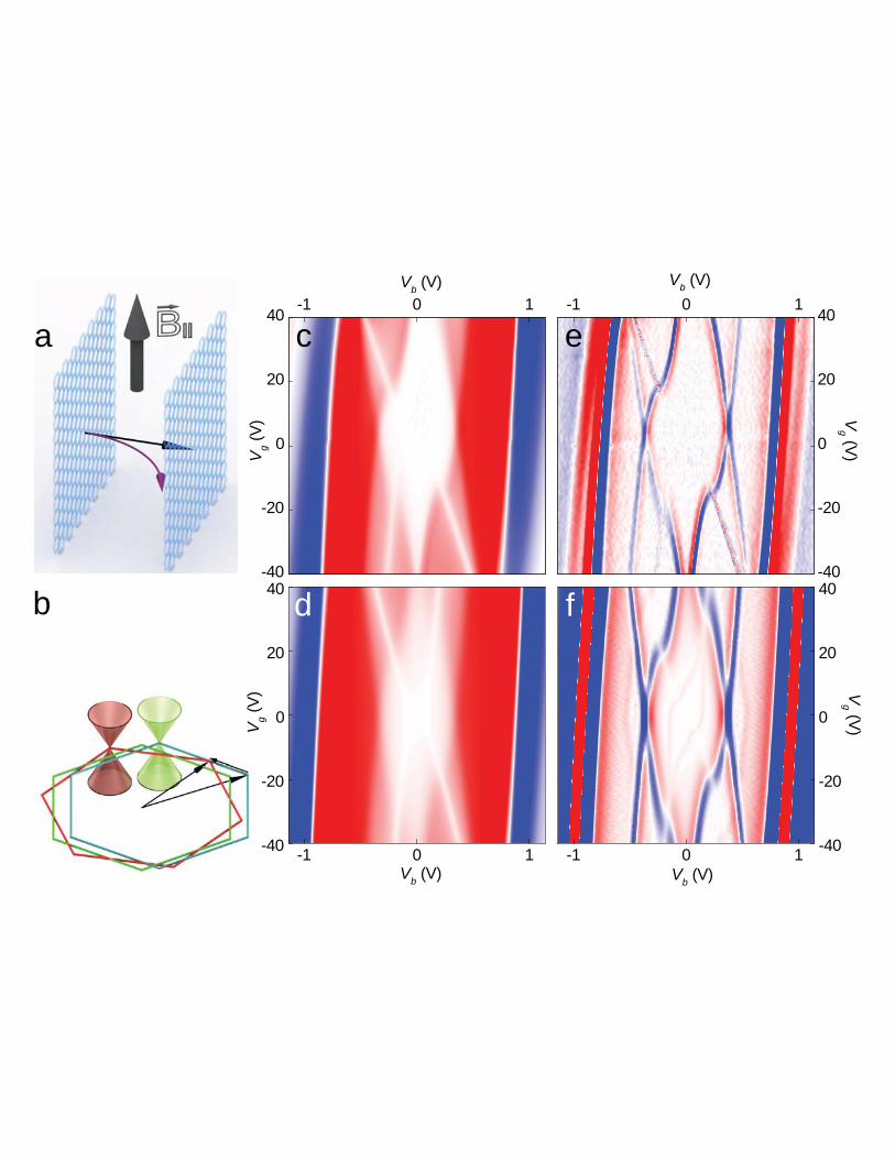
A schematic diagram of our transistor is drawn on Fig. 1a, while Fig. 2a shows the dependence of the
current density, J, measured at 2K as a function of the bias voltage, Vb, for three different values of the
gate voltage, Vg. We observe a strong peak in J(Vb), followed by a region of NDC, both of which persist
up to room temperature. We attribute this peak to resonant tunnelling of carriers between the two
graphene electrodes with momentum conservation. In order to display in more detail the key features of
the device characteristics, Fig. 2b and c present colour scale contour maps of the dependence of the
differential conductance (dI/dVb) and d2I/dVb2 on Vb and Vg; here I is current. In Fig. 2b the regions of the
NDC are shown as blue areas. Furthermore, weaker resonances can be seen as a transition from pink to
red colours.
In order to explain the physics of the electron tunnelling in these devices, we used a theoretical model22-25
which takes into account the unique band structure of graphene and the physics of the eigenstates of the
massless Dirac fermions in the graphene layers on the device characteristics. The results of this model,
shown in Fig. 2d-f, reproduce the measured device characteristics. Here, we focus on the case of a small
angular misalignment, , of the two graphene lattices, see Fig. 1a, which corresponds to a rotation of the
two graphene Brillouin zones in momentum space, see Fig. 1b. In particular, the neutrality points at the
six K-points of the Brillouin zone, (where i=1,2,3 identify equivalent corners, ± distinguishes
between the K and K′ valleys and is the reduced Plank constant) are displaced by the wavevectors
.
The resulting intersection of the Dirac cones which visualise the conditions for resonant tunnelling of
electrons between two layers are shown in Fig. 1c-e for characteristic regimes of bias voltage. They
display the energy shift of both Dirac cones and Fermi levels as the carrier concentrations in the two
graphene layers change due to changes in the bias and gate voltages. Fig. 1c and, especially, Fig. 1d
illustrate how the conditions for resonant tunnelling can be satisfied. The case shown in Fig. 1d is of
particular importance, since the tunnel current is maximized when the momentum difference, , is

4
compensated by changing electrostatically the energy of the two Dirac cones by an amount
(valid for small , here is the graphene Fermi velocity). In this case the conical dispersions
in the two layers intersect along a straight line and a large fraction of the states along that line are
occupied in one layer and empty in the other layer, thus facilitating a large resonant tunnel current. Fig. 1e
demonstrates the case at yet higher bias voltage between the top and bottom graphene layers, where the
in-plane momentum is conserved only for a small number of states (far away from the Fermi levels of the
two graphene electrodes), thus, leading to the reduction in the current. We now consider the detailed
features of the measured differential conductance map, Fig.2c. The red and blue dashed lines in Fig. 2c
are theoretical simulations and correspond to the situation when Fermi levels of the top and bottom
graphene layers pass through Dirac points. These lines are universal features for all graphene-to-graphene
tunnelling systems regardless of their relative alignment, and can be obtained using a simple electrostatic
model (see Supplementary Section 2). The density of states (DoS) of graphene close to the Dirac point
varies linearly with chemical potential, i.e., | |. Thus, the tunnel conductance decreases when the
graphene Fermi level crosses the Dirac point due to the DoS vanishing at this point. The small but finite
conductance at the Dirac point is due to charge inhomogeneity, which results in the DoS smearing at the
Dirac point and remaining non-zero26.
The set of green lines in Fig. 2b and c trace the low bias and relatively weak resonance in the device
characteristics when the chemical potential of one of the graphene layers reaches the point where the two
Dirac cones begin to overlap (Fig. 1c). These four lines satisfy the condition ( ) ⁄ .
The intersection of these lines at Vg = 0 provides a good measure of the momentum mismatch
⁄ , and therefore gives an accurate estimate of the misalignment angle, θ. For example, for the
device shown in Fig. 2, we estimate that θ = 1.8°. It is interesting to note the geometry of the intersection
of the two Dirac cones under the conditions shown in Fig. 1c and Fig. 2: they form hyperbolic solutions.
The wavevectors of the Dirac plane waves lie on three hyperbolae obtained by 120° rotations of these
hyperbolic solutions (see Supplementary Section 1). The solutions remain hyperbolic for | | .
This low bias resonance does not lead to NDC, but it does give rise to a significant increase in
conductance, as shown in Fig. 2b.

5
The voltage dependence of the main resonance peak is shown as yellow lines in Fig. 2b and c. In this
case, the Dirac cones are shifted by so that the intersection of the cones is a straight line
(i.e. the wavevectors of the Dirac plane waves lie on straight lines), see Fig. 1d. In this situation,
momentum is conserved for tunnelling electrons at all energies between and , thus giving rise to a
strong peak in the current density at resonance. When the Dirac cones are displaced further beyond this
resonant condition, that is for | | , the curve of intersection of the two Dirac cones becomes
an ellipse (Fig. 1e). As a result, the wavevectors lie on three ellipses. In contrast to the hyperbolic and
linear solutions, the elliptic solutions are bound – only wavevectors limited by these ellipses can
contribute to current density. The reduction of the current once the Dirac cones are shifted off-resonance
is the physical mechanism which gives rise to the negative differential conductance region beyond the
resonant peak.
The main resonant peak, which would be Dirac-delta like in the absence of broadening, has a finite width
due to the presence of short-range scatterers, charge inhomogeneity in the graphene layers or orientational
disorder between two graphene layers because of bubble formation1. Furthermore, since this mechanism
of resonant tunnelling relies on momentum conservation, the position of the resonant peak and the peak-
to-valley ratio are only weakly dependent on temperature. This mechanism for NDC is only possible in
the graphene-graphene tunnelling system; for example, if one or both electrodes are replaced with bilayer
graphene, then, due to the parabolic dispersion relation, the extended linear intersection is no longer
possible. Note that in the modelled J-Vb characteristics (Fig 2d-f) we take into account the chirality of
electrons (the momentum-dependent phase shift of the wavefunction on the two sublattices in graphene,
see Supplementary Sections 1 and 2). In the absence of strain, however, the results stay qualitatively the
same.
In order to confirm our proposed mechanism of resonant tunnelling we performed additional
measurements in which a magnetic field, , was applied parallel to the graphene layers, i.e.
perpendicular to the tunnel current. Classically, the electron tunnelling between two 2D electrodes
through a barrier of thickness d will acquire an additional in-plane momentum , due to the action

6
of the Lorentz force27,28. Depending on the orientation of the magnetic field with respect to
crystallographic directions of the two graphene layers, the magnitude of the wavevectors,
[
]
differs for each of the six Dirac cones at the corners of Brillouin zone.
Figure 3 presents the measured (c) and calculated (d) tunnel conductance maps in the presence of a strong
in-plane magnetic field, . In Fig. 3e, the measured contour maps at zero field (Fig. 2b) and with (Fig.
3c) magnetic field ( = 15 T) are subtracted from each other. This “difference map” reveals that the bias
positions of the resonances, which correspond to various momentum conservation conditions, are shifted
significantly by the in-plane field. At the same time, the position of the μT = 0 and μB = 0 resonances
(which are insensitive to momentum conservation) in the dI/dVb contour maps are almost unchanged. The
fact that the in-plane magnetic field affects only the resonances where momentum conservation processes
are involved, rules out the possible artefacts, such as a small perpendicular component of magnetic field.
One of the celebrated applications of devices with NDC is their use as high frequency oscillators, which
are typically constructed by connecting an external resonant circuit to the device. To this end, as a proof-
of-principle we have built such an oscillator by adding an inductance in series with our resonant
tunnelling device, while utilising the intrinsic and parasitic capacitance (Ctot) as a capacitance of LC
circuit, see Figure 4b. When the bias and gate voltages are tuned to the NDC region, the device undergoes
stable sine-wave oscillations, see Fig. 4a,c. The oscillation frequency can be tuned by varying the
parameters of the external circuit, see Fig. 4b.
The operation of an NDC-based LC resonator can be understood as follows. Once excited, the LC circuit
produces damped oscillations which rapidly decay to zero. This is mainly due to the internal dissipative
resistance, R, of the resonator and other losses. When the tunnel transistor operates in the NDC region, its
negative resistance cancels the internal lossy resistance, thus supporting continuous stable oscillations at
the resonant frequency of the LC circuit. Interestingly, the shape of the J-Vb curve changes in the region
of stable oscillations, as compared with the case without the LC circuit, see Figure 4a (likely, due to the

7
change in the asymmetric rectification of radio-frequency oscillations in the strongly nonlinear J-Vb
region).
To summarize, by aligning the crystallographic orientation of the two graphene layers in a graphene-
hBN-graphene heterostructure, we have demonstrated that resonant tunnelling with both energy and
momentum conservation can be achieved. This results in strong NDC which persists up to room
temperature. The bias position of the resonance can be controlled by the relative orientation between the
two graphene crystalline lattices and by external magnetic field. Our tunnel diodes produce stable
oscillations in the MHz frequency range, limited mainly by the parasitic capacitance between the contact
pads of our devices and the underlying Si gate. Much higher frequencies could be reached by reducing
this parasitic capacitance and that of the external circuit. Even higher frequencies could also be achieved
by fabricating a device in a slot antenna configuration, where the slot acts as a resonator with resonance
frequency determined by the geometry of the slot. Moreover, our tunnel devices are free of the
fundamental limitation intrinsic to conventional double barrier resonant tunnelling devices, namely the
relatively long carrier dwell time (~ps) in the quantum well as compared to the time to transit the barrier
(~fs). This suggests that such tunnel circuits can be potentially scaled to operate in the THz regime.
Methods
Device fabrication. The heterostructures are made by means of a standard dry-transfer procedure of mechanically-
exfoliated graphene and hBN layers5,29, with the important additional step that the lattices of the top and bottom
graphene flakes are aligned to within 2o of each other. We used mechanically torn graphene flakes30 with well-
defined facets and were able to distinguish between the armchair and zig-zag edges by comparing the intensity of
the Raman D peak from the edges31. This allowed us to know the crystallographic orientation of both top and bottom
graphene, thus achieving a high level of alignment (see Supplementary Section 3 for details). An independent proof
of the crystallographic alignment between the two graphene electrodes comes from the measurements of the
broadening of the Raman 2D peak for the two graphene flakes. Such broadening serves as a measure of the rotation
angle between graphene and underlying hBN12,32, and allows one to calculate the relative angle between the
crystallographic directions for the two graphene electrodes (see Supplementary Section 3 for details). In order to
improve its electronic quality, the bottom graphene electrode was placed on a thick layer of hBN overlaying the
SiO2/Si substrate, with the heavily doped Si wafer acting as a back gate33. The two graphene layers were

8
independently contacted with Cr/Au metallization. We chose the thickness of hBN tunnel barriers to be 4
monolayers, which allows us to work in a comfortable range of current densities and bias voltages. Note, that the
current density can be dramatically increased (4-5 orders of magnitude)7,8 if thinner (2-3 layers) hBN or a material
with lower tunnel barrier (like WS2) is utilised9,10,18.
References
1 Geim, A. K. & Grigorieva, I. V. Van der Waals heterostructures. Nature 499, 419-425
(2013).
2 Novoselov, K. S. Nobel Lecture: Graphene: Materials in the Flatland. Reviews of Modern
Physics 83, 837-849 (2011).
3 Novoselov, K. S. et al. Electric field effect in atomically thin carbon films. Science 306,
666-669 (2004).
4 Novoselov, K. S. et al. Two-dimensional atomic crystals. Proceedings of the National
Academy of Sciences of the United States of America 102, 10451-10453 (2005).
5 Ponomarenko, L. A. et al. Tunable metal–insulator transition in double-layer graphene
heterostructures. Nature Physics 7, 958–961 (2011).
6 Gorbachev, R. V. et al. Strong Coulomb drag and broken symmetry in double-layer
graphene. Nature Physics 8, 896-901 (2012).
7 Lee, G. H. et al. Electron tunneling through atomically flat and ultrathin hexagonal boron
nitride. Applied Physics Letters 99, 243114 (2011).
8 Britnell, L. et al. Electron tunneling through ultrathin boron nitride crystalline barriers.
Nano Letters 12, 1707-1710 (2012).
9 Britnell, L. et al. Field-effect tunneling transistor based on vertical graphene
heterostructures. Science 335, 947-950 (2012).
10 Georgiou, T. et al. Vertical field-effect transistor based on graphene-WS2 heterostructures
for flexible and transparent electronics. Nature Nanotechnology 8, 100-103 (2013).
11 Britnell, L. et al. Strong light-matter interactions in heterostructures of atomically thin
films. Science 340, 1311-1314 (2013).

9
12 Woods, C. R. et al. Commensurate-incommensurate transition in graphene on hexagonal
boron nitride. Nature Physics 10, 451-456 (2014).
13 Xue, J. M. et al. Scanning tunnelling microscopy and spectroscopy of ultra-flat graphene on
hexagonal boron nitride. Nature Materials 10, 282-285 (2011).
14 Yankowitz, M. et al. Emergence of superlattice Dirac points in graphene on hexagonal
boron nitride. Nature Physics 8, 382-386 (2012).
15 Ponomarenko, L. A. et al. Cloning of Dirac fermions in graphene superlattices. Nature 497,
594-597 (2013).
16 Dean, C. R. et al. Hofstadter's butterfly and the fractal quantum Hall effect in moire
superlattices. Nature 497, 598-602 (2013).
17 Hunt, B. et al. Massive Dirac fermions and Hofstadter butterfly in a van der Waals
heterostructure. Science 340, 1427-1430 (2013).
18 Yang, H. et al. Graphene barristor, a triode device with a gate-controlled Schottky barrier.
Science 336, 1140-1143 (2012).
19 Haigh, S. J. et al. Cross-sectional imaging of individual layers and buried interfaces of
graphene-based heterostructures and superlattices. Nature Materials 11, 764–767 (2012).
20 Britnell, L. et al. Resonant tunnelling and negative differential conductance in graphene
transistors. Nature Communications 4, 1794 (2013).
21 Ponomarenko, L. A. et al. Field-effect control of tunneling barrier height by exploiting
graphene's low density of states. Journal of Applied Physics 113, 136502 (2013).
22 Feenstra, R. M., Jena, D. & Gu, G. Single-particle tunneling in doped graphene-insulator-
graphene junctions. Journal of Applied Physics 111, 043711 (2012).
23 de la Barrera, S. C., Gao, Q. & Feenstra, R. M. Theory of graphene–insulator–graphene
tunnel junctions. Journal of Vacuum Science and Technology B 32, 04E101 (2014).
24 Wallbank, J. R. Electronic properties of graphene heterostructures with hexagonal crystals .
(Springer, 2014).
25 Brey, L. Coherent tunneling and negative differential conductivity in a graphene/h-
BN/graphene heterostructure. Physical Review Applied 2, 014003 (2014).

10
26 Martin, J. et al. Observation of electron-hole puddles in graphene using a scanning single-
electron transistor. Nature Physics 4, 144-148 (2008).
27 Hayden, R. K. et al. Probing the hole dispersion curves of a quantum well using resonant
magnetotunneling spectroscopy. Physical Review Letters 66, 1749-1752 (1991).
28 Falko, V. I. & Meshkov, S. V. On resonant oscillations in current-voltage characteristics of
double-barrier heterostructures. Semiconductor Science and Technology 6, 196-200 (1991).
29 Dean, C. R. et al. Boron nitride substrates for high-quality graphene electronics. Nature
Nanotechnology 5, 722-726 (2010).
30 Sen, D., Novoselov, K. S., Reis, P. M. & Buehler, M. J. Tearing graphene sheets from
adhesive substrates produces tapered nanoribbons. Small 6, 1108-1116 (2010).
31 Neubeck, S. et al. Direct determination of the crystallographic orientation of graphene edges
by atomic resolution imaging. Applied Physics Letters 97, 053110 (2010).
32 Eckmann, A. et al. Raman fingerprint of aligned graphene/h-BN superlattices. Nano Letters
13, 5242–5246 (2013).
33 Mayorov, A. S. et al. Micrometer-Scale Ballistic Transport in Encapsulated Graphene at
Room Temperature. Nano Letters 11, 2396-2399 (2011).
Acknowledgements
This work was supported by the European Research Council, EC-FET European Graphene Flagship,
Engineering and Physical Sciences Research Council (UK), the Leverhulme Trust (UK), the Royal
Society, U.S. Office of Naval Research, U.S. Air Force Office of Scientific Research, U.S. Army
Research Office and RS-RFBR, grants number 14-02-00792 and 13-02-92612 (Russian Federation). Y.-
J.K. was supported by the Global Research Lab Program (2011-0021972) through the National Research
Foundation of Korea funded by the Ministry of Science, ICT & Future, Korea.
Author contributions
J.S.T., Y.C., and Y.J.K. fabricated devices, A.M. carried out measurements and analysed the results,
J.R.W., M.T.G., T.M.F., V.I.F and L.E. provided theoretical support, K.W. and T.T. provided hBN
crystals, S.L.W., F.W., and C.R.W. performed AFM and Raman measurements, R.V.G., V.E.M., S.V.M.,

11
M.J.Z., E.E.V., and O.M. helped with experiments and/or writing the paper, A.M., K.S.N. and L.E. wrote
the manuscript. Sections 1 and 2 of Supplementary Information was written by J.R.W. and V.I.F. All
authors contributed to discussions.
Additional information
Supplementary information is available in the online version of the paper. Reprints and permissions
information is available online at ww.nature.com/reprints. Correspondence and requests for materials
should be addressed to K.S.N. and L.E.
Competing financial interests
The authors declare no competing financial interests.
Figure Legends
Figure 1: Schematic representation of our device and its band structure. a) Device schematics with the
angle θ between two graphene layers (separated by a BN tunnel barrier shown in light blue) exaggerated.
The heterostructure is placed on a SiOx/Si substrate (magenta/light grey colours) serving as an
electrostatic gate while both graphene layers are independently contacted by Cr/Au metallization (yellow
coloured on the figure) b) A rotation by θ of the two graphene layers in real space corresponds to the
momentum shift between two Dirac points. Diagrams c-e represent the relative alignment between
top (left cones) and bottom (right cones) graphene Dirac points; the boundary between magenta (empty
states) and blue (filled states) colours marks the Fermi level.
Figure 2. The device characteristics at 2K. Panels (a)-(c): experiment; (d)-(f): theoretical simulations.
a,d) Current density-voltage curves at different Vg (red, green and blue lines for +40, 0 and -40V,
respectively). b,e) Conductivity dI/dV plots as a function of Vb and Vg (colour scale is blue to white to red:
-5S to 0S to 5S). c,f) |d2I/dV2| plots as a function of Vb and Vg (colour scales are arbitrary and matched
for c and f). The dashed lines in b) and c) are theoretical simulations and correspond to different resonant
conditions. Red and blue lines correspond to events when the Fermi level in one of the graphene layers

12
passes through the Dirac point. The green lines correspond to the event depicted in Fig. 1c, and the
yellow line – to the event depicted in Fig. 1d. Device characteristics: active area of ≈8 μm2, hBN barrier
thickness is 1.4nm (4 layers), θ ≈ 1.8°.
Figure 3. Effect of in-plane magnetic field on resonant tunnelling, same device as in Figure 2. Panels c)
and e) are experimental data, panels d) and f) – theoretical modelling. a) Trajectories of the charged
quasiparticles tunnelling from top (left) to bottom (right) graphene layers in zero (black arrow) and finite
(purple arrow) magnetic field (depicted as thick black arrow) due to Lorentz force. b) The resulting shift
(cf. green and blue hexagons) of Fermi surface due to an in-plane magnetic field, exaggerated for clarity.
Here red and green/blue hexagons represent corners of the Brillouin zones for top and bottom graphene
layers, respectively. c,d) dI/dV maps measured with 15T in-plane magnetic field applied (colour scale is
blue to white to red: -4S to 0S to 4S), e,f) difference between dI/dV maps with and without in-plane B
field (colour scale is blue to white to red: -0.4S to 0S to 0.4S).
Figure 4. Radio-frequency oscillator based on resonant tunnelling transistor, T=300K. a) J(Vb)
characteristics with (blue, solid, L=1mH) and without (black, dashed, L=0H) external LC circuit. The red
curve shows the Vb-dependence of the peak-to-peak amplitude of the oscillations. b) Resonant frequency
of the oscillator (schematics shown on the top left inset) vs. inductance of the LC circuit. For this device
the total capacitance of the assembly was estimated from a simple circuit model (see top left inset) to be
65pF, red line – model fit to the data. Bottom right inset: Vout as a function of time for L=1mH. c) dI/dVb
map measured with a 330μH inductance (red to white to blue, -0.7μS to 0μS to 0.7μS) and d)
corresponding amplitude map (red to yellow to violet, 0.5V to 0.26V to 0.03V). Device structure: active
area of ≈120 μm2, hBN spacer =1.4nm (4 layers), θ ≈ 0.9°.

a b
c d e
�
��+1
��-
3
��+3
��-
2
��+2
��-
1

-0.4
-0.2
0.0
0.2
0.4
-1
0
1J
(µA/
µm2 )
a d
J(a
.u.)
-40
-20
0
20
40b
Vg
(V)
e
-1 0 1-40
-20
0
20
40c
Vb (V)
Vg
(V)
-1 0 1
f
Vb (V)
-40
-20
0
20
40-1 0 1
b
Vb (V)V
g(V
)
ca-1 0 1
-40
-20
0
20
40e
Vb (V)
Vg (V)
-1 0 1-40
-20
0
20
40 d
Vg
(V)
Vb (V)-1 0 1 -40
-20
0
20
40f
Vg (V)
Vb (V)

0.0
0.1
0.2
0.30.0 0.5 1.0
-0.2
0.0
0.2
-5 0 5
50 100
1
2
Vb (V)
J(µ
A/µm
2 )
a
0.0
0.2
0.4
0.6
Oscillation
amplitude
(V)
Time (µs)
Vou
t(V
)
b-R
Vout
CtotVb
f0 (MH
z)
L-1/2 (H-1/2)
L
-1.0 -0.5 0.0 0.5 1.0-40
-20
0
20
40 c
Vb (V)
Vg
(V)
-1.0 -0.5 0.0 0.5 1.0-40
-20
0
20
40d
Vg (V)
Vb (V)