tv123wam-nd0 pebble creek product spec boe … · 17.0 handling sop 33. a4(210 x 297) page ... lux...
TRANSCRIPT

A4(210 X 297)
SPEC. NUMBER PRODUCT GROUP
LCM
PAGE
TV123WAM-ND0
Product Specification
Rev. P0
A4(210 X 297)
OF 32
PROPRIETARY NOTETHIS SPECIFICATION IS THE PROPERTY OF BOE BJ AND SHALL NOT BEREPRODUCED OR COPIED WITHOUT THE WRITTEN PERMISSION OF BOE BJ AND MUST BE RETURNED TO BOE BJ UPON ITS REQUEST
HEFEI BOE OPTOELECTRONICS TECHNOLOGY CO.,LTD
R2013-9024-O(1/3)
Rev.
P0
ISSUE DATE
1

A4(210 X 297)
SPEC. NUMBER PRODUCT GROUP
LCM
PAGE
A4(210 X 297)
OF 32
PROPRIETARY NOTETHIS SPECIFICATION IS THE PROPERTY OF BOE BJ AND SHALL NOT BEREPRODUCED OR COPIED WITHOUT THE WRITTEN PERMISSION OF BOE BJ AND MUST BE RETURNED TO BOE BJ UPON ITS REQUEST
R2013-9024-O(2/3)
Rev.
P0
ISSUE DATE
REV.
ECN No. DESCRIPTION OF CHANGES DATE PREPARED
P0 - Initial version 2016/9/5 Tian Wei
2

A4(210 X 297)
PAGE
REV ISSUE DATEPRODUCT GROUP
LCM PRODUCT
OF 32SPEC. NUMBER SPEC. TITLE
TV123WAM-ND0 Product Specification 3
P0
R2013-9024-O(3/3) 3
Contents
No. Items Page
1.0 General Description 4
2.0 Absolute Maximum ratings 6
3.0 Electrical specifications. 7
4.0 Optical specifications. 9
5.0 Interface Connection 14
6.0 Signal Timing Specification 18
7.0 Input Signals, Display Colors & Gray Scale of Colors 20
8.0 Power Sequence 21
9.0 Connector description 22
10.0 Mechanical Characteristics 23
11.0 Reliability Test 24
12.0 Handling & Cautions. 24
13.0 Label 25
14.0 Packing information 27
15.0 Mechanical Outline Dimension 28
16.0 EDID Table 30
17.0 Handling SOP 33

A4(210 X 297)
PAGE
REV ISSUE DATEPRODUCT GROUP
LCM PRODUCT
OF 32SPEC. NUMBER SPEC. TITLE
TV123WAM-ND0 Product Specification 4
P0
R2013-9024-O(3/3) 4
1.0 GENERAL DESCRIPTION
1.1 Introduction
12.3 ‘s TFT LCD module uses amorphous silicon TFT‘s (Thin Film Transistors) as anactives witching devices. This module has a 12.3 inch diagonally measured active areawith WUXGA+ resolutions (1920 horizontal by 1280 vertical pixel array). Each pixel isdivided into RED, GREEN, BLUE dots which are arranged in vertical Stripe. The TFT‐LCDpanel used for this module is a low re‐flection and higher color type. Therefore, thismodule is suitable for TPC. The LED Driver for back‐light driving is not built in thismodel. All input signals are eDP1.4 interface compatible.
1.2 Features
2‐in‐1Business Tablet Thin and light weight——156g Max;1.96mm Max High color gamut——sRGB100% coverage Green Product (RoHS & Halogen free product) On board LED Driving circuit
BACK LIGHT (Fluorescent Lamp)
Gate D
river
Source Driver
TFT LCD Panel1920 ×1280
eDP Rx+
T/CON+
Mini‐LVDS Tx
DC/DCGammaVcom
Connecto
r
eDPInput Signal
VDD
LED Lighting Bar
1
LED Driver
A4(210 X 297)
PAGE
REV ISSUE DATEPRODUCT GROUP
LCM PRODUCT
OF 32SPEC. NUMBER SPEC. TITLE
TV123WAM-ND0 Product Specification 5
P0
R2013-9024-O(3/3) 5
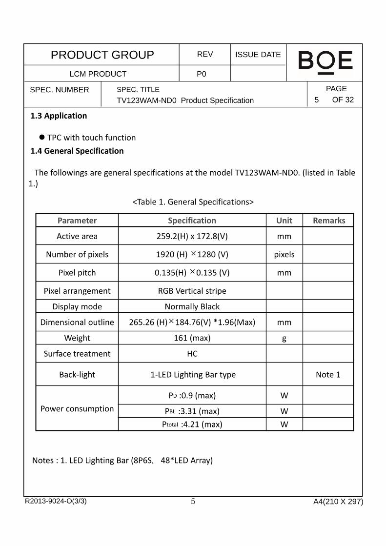
1.4 General Specification
The followings are general specifications at the model TV123WAM‐ND0. (listed in Table 1.)
Notes : 1. LED Lighting Bar (8P6S,48*LED Array)
<Table 1. General Specifications>
1.3 Application
TPC with touch function
Parameter Specification Unit Remarks
Active area 259.2(H) x 172.8(V) mm
Number of pixels 1920 (H) ×1280 (V) pixels
Pixel pitch 0.135(H) ×0.135 (V) mm
Pixel arrangement RGB Vertical stripe
Display mode Normally Black
Dimensional outline 265.26 (H)×184.76(V) *1.96(Max) mm
Weight 161 (max) g
Surface treatment HC
Back‐light 1‐LED Lighting Bar type Note 1
Power consumption
PD :0.9 (max) W
PBL :3.31 (max) W
Ptotal :4.21 (max) W

A4(210 X 297)
PAGE
REV ISSUE DATEPRODUCT GROUP
LCM PRODUCT
OF 32SPEC. NUMBER SPEC. TITLE
TV123WAM-ND0 Product Specification 6
P0
R2013-9024-O(3/3) 6
2.0 ABSOLUTE MAXIMUM RATINGSThe followings are maximum values which, if exceed, may cause faulty operation ordamage to the unit. The operational and non‐operational maximum voltage and cur
rent values are listed in Table 3.
Parameter Symbol Min. Max. Unit Remarks
LCM Power Supply Voltage VDD ‐0.3 4.0 VNote 1
LCM Logic Supply Voltage VIN Vss‐0.3 VDD+0.3 V
Operating Temperature TOP 0 +50 ℃Note 2
Storage Temperature TST ‐20 +60 ℃
Notes : 1. Permanent damage to the device may occur if maximum values are exceededfunctional operation should be restricted to the condition described under normaloperating conditions.
2. Temperature and relative humidity range are shown in the figure below.95 % RH Max. ( 40 OC ≥ Ta)Maximum wet ‐ bulb temperature at 39 OC or less. (Ta > 40 OC) No condensation.
Ta=25+/‐2°C< Table 3. Absolute Maximum Ratings>
Operating Range
Stor
age
Ran
ge
-40 -20 0 20 40 60 80
Temperature (℃)
(40, 95)
(50, 80)
(60, 27)
100
80
60
40
20
90
Relative Humudity
5
Stor
age
Ran
ge

A4(210 X 297)
PAGE
REV ISSUE DATEPRODUCT GROUP
LCM PRODUCT
OF 32SPEC. NUMBER SPEC. TITLE
TV123WAM-ND0 Product Specification 7
P0
R2013-9024-O(3/3) 7
3.0 ELECTRICAL SPECIFICATIONS
3.1 Electrical Specifications
< Table 4. Electrical specifications >
Notes : 1. The supply voltage is measured and specified at the interface connector of LCM. The current draw and power consumption specified is for 3.3V 60Hz at 25℃. (Max: 8*6 Mosaic pattern)
Ta=25+/‐2°C
Parameter Min. Typ. Max. Unit Remarks
Power Supply Voltage VDD 3.0 3.3 3.6 V Note 1
Permissible Input Ripple Voltage
VRF ‐ ‐ 300 mV At VDD = 3.3V
Power Supply Current IDD ‐ 191 242 mA Note 1
Positive‐going Input Threshold Voltage
VIT+ ‐ ‐ 100 mVVcm = 1.2V typ
.Negative‐going Input Threshold Voltage
VIT‐ ‐100 ‐ ‐ mV
Differential Input Voltage VID ‐ ‐ 600 mV
Power Consumption
PD ‐ 0.63 0.8 W Note 1
PBL ‐ 3.28 3.31 W
Ptotal ‐ 3.91 4.21 W

A4(210 X 297)
PAGE
REV ISSUE DATEPRODUCT GROUP
LCM PRODUCT
OF 32SPEC. NUMBER SPEC. TITLE
TV123WAM-ND0 Product Specification 8
P0
R2013-9024-O(3/3) 8
3.2 Backlight Unit
Parameter Min. Typ. Max. Unit Remarks
LED Forward Voltage VF ‐ ‐ 6.2 V IF = 11.1mA
LED Forward Current IF ‐ 11.1 mA ‐
LED Power Consumption PLED 3.31 W Note 1
LED Life‐Time N/A 15,000 ‐ ‐ Hour
< Table 5. LED Driving guideline specifications >
Notes : 1. The LED Life‐time define as the estimated time to 50% degradation of initial luminous.
Ta=25+/‐2°C

A4(210 X 297)
PAGE
REV ISSUE DATEPRODUCT GROUP
LCM PRODUCT
OF 32SPEC. NUMBER SPEC. TITLE
TV123WAM-ND0 Product Specification 9
P0
R2013-9024-O(3/3) 9
3.3 LED structure 8P*6S

A4(210 X 297)
PAGE
REV ISSUE DATEPRODUCT GROUP
LCM PRODUCT
OF 32SPEC. NUMBER SPEC. TITLE
TV123WAM-ND0 Product Specification 10
P0
R2013-9024-O(3/3) 10
4.0 OPTICAL SPECIFICATION
4.1 OverviewThe test of Optical specifications shall be measured in a dark room (ambient luminance 1lux and temperature = 252℃) with the equipment of Luminance meter system (Goniometersystem and TOPCON BM‐5) and test unit shall be located at an approximate distance50cm from the LCD surface at a viewing angle of θ and Φ equal to 0. We refer to θØ=0(=θ3 ) as the 3 o’clock direction (the “right”), θØ=90 (= θ12 ) as the 12 o’clock direction(“upward”), θØ=180 (= θ9 ) as the 9 o’clock direction (“left”) andθØ=270(= θ6 ) as the 6 o’clock direction (“bottom”). While scanning θand/or Ø, the centerof the measuring spot on the Display surface shall stay fixed. The backlight should beoperating for 30 minutes prior to measurement. VDD shall be 3.3+/‐ 0.3V at 25C.Optimum viewing angle direction is 6 ’clock.
<Table 6. Optical Specifications>4.2 Optical Specifications
Parameter Symbol Condition Min. Typ. Max. Unit Remark
Viewing Angle range
HorizontalΘ3
CR > 10
80 85 ‐ Deg.
Note 1Θ9 80 85 ‐ Deg.
VerticalΘ12 80 85 ‐ Deg.
Θ6 80 85 ‐ Deg.
Luminance Contrast ratio CR Θ = 0 ‐ 1200 ‐ Note 2Luminance of
White5 Points Yw
Θ = 0ILED = 11.1mA
360 400 ‐ cd/m2 Note 3
White Luminance uniformity
5 Points ΔY5 80% ‐ ‐Note 4
13 Points ΔY13 65% ‐ ‐
White Chromaticityxw Θ = 0
0.28 0.31 0.34 ‐
Note 5
yw 0.3 0.33 0.36 ‐
Reproductionof color
RedxR
Θ = 0 ‐0.03
0.646
+0.03
‐
yR 0.334 ‐
GreenxG 0.295 ‐
yG 0.612 ‐
BluexB 0.150 ‐
yB 0.064 ‐
Color Gamut ‐ 73.5 ‐ % NTSCResponse Time(Rising + Falling)
TRTTa= 25 CΘ = 0 ‐ 25 30 ms Note 6
Cross Talk CT Θ = 0 ‐ ‐ 2.0 % Note 7

A4(210 X 297)
PAGE
REV ISSUE DATEPRODUCT GROUP
LCM PRODUCT
OF 32SPEC. NUMBER SPEC. TITLE
TV123WAM-ND0 Product Specification 11
P0
R2013-9024-O(3/3) 11
CR =Luminance when displaying a white raster
Luminance when displaying a black raster
Notes :1. Viewing angle is the angle at which the contrast ratio is greater than 10. The viewing angles are determined for the horizontal or 3, 9 o’clock direction and the vertical or 6, 12 o’clock direction with respect to the optical axis which is normal to the LCD surface(see FIGURE 1).
2. Contrast measurements shall be made at viewing angle of Θ= 0 and at the center of the LCDsurface. Luminance shall be measured with all pixels in the view field set first to white, then tothe dark (black) state .(see FIGURE 1) Luminance Contrast Ratio (CR) is defined mathematically.
3. (with TP)Center Luminance of white is defined as luminance values of 5 point average acrossthe LCD surface. Luminance shall be measured with all pixels in the view field set firstto white. This measurement shall be taken at the locations shown in FIGURE 2 for atotal of the measurements per display.
4. The White luminance uniformity on LCD surface is then expressed as : ΔY =Minimum Luminance of 5(or 13) points / Maximum Luminance of 5(or 13) points.(see FIGURE 2 and FIGURE 3).
5. The color chromaticity coordinates specified in Table 5 shall be calculated from thespectral data measured with all pixels first in red, green, blue and white. Measurements shall bemade at the center of the panel.
6. The electro‐optical response time measurements shall be made as FIGURE 4 byswitching the “data” input signal ON and OFF. The times needed for the luminance tochange from 10% to 90% is Tr, and 90% to 10% is Td.
7. Cross‐Talk of one area of the LCD surface by another shall be measured bycomparing the luminance (YA) of a 25mm diameter area, with all display pixels set to agray level, to the luminance (YB) of that same area when any adjacent area is drivendark.(See FIGURE 5).

A4(210 X 297)
PAGE
REV ISSUE DATEPRODUCT GROUP
LCM PRODUCT
OF 32SPEC. NUMBER SPEC. TITLE
TV123WAM-ND0 Product Specification 12
P0
R2013-9024-O(3/3) 12
Figure 1. Measurement Set Up
Figure 2. White Luminance and Uniformity Measurement Locations (5 points)
Optical characteristics measurement setup
Center of the screen
TFT‐LCD module LCD panel
Photo detector(TOPCON BM‐5A)
50 cm Field = 2 o
4.3 Optical measurements
Center Luminance of white is defined as luminance values of center 5 points across the LCD surface. Luminance shall be measured with all pixels in the view field set first to white. This measurement shall be taken at the locations shown in FIGURE 2 for a total of the measurements per display.
A4(210 X 297)
PAGE
REV ISSUE DATEPRODUCT GROUP
LCM PRODUCT
OF 32SPEC. NUMBER SPEC. TITLE
TV123WAM-ND0 Product Specification 13
P0
R2013-9024-O(3/3) 13
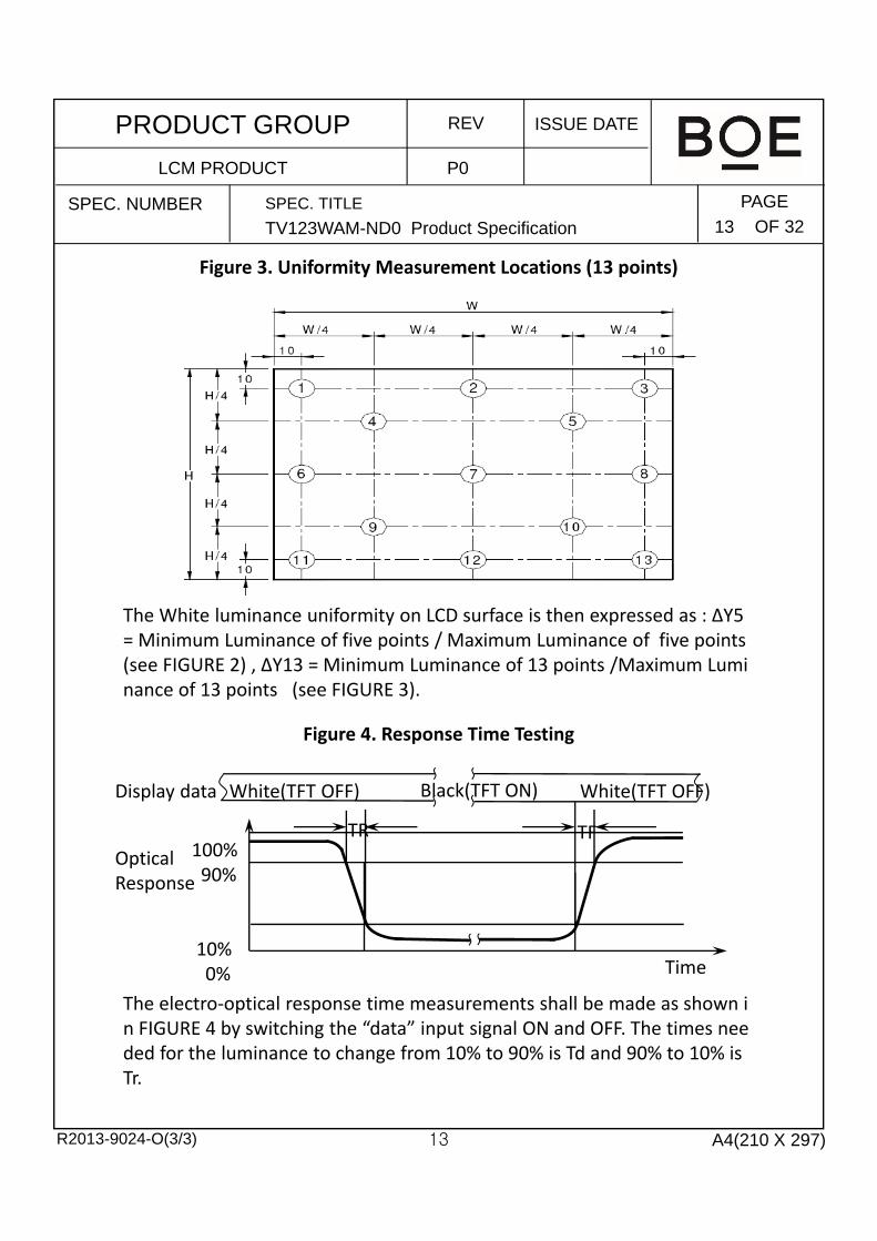
Figure 3. Uniformity Measurement Locations (13 points)
Figure 4. Response Time Testing
The White luminance uniformity on LCD surface is then expressed as : ΔY5 = Minimum Luminance of five points / Maximum Luminance of five points (see FIGURE 2) , ΔY13 = Minimum Luminance of 13 points /Maximum Luminance of 13 points (see FIGURE 3).
The electro‐optical response time measurements shall be made as shown in FIGURE 4 by switching the “data” input signal ON and OFF. The times needed for the luminance to change from 10% to 90% is Td and 90% to 10% is Tr.
Display data
OpticalResponse
Black(TFT ON)White(TFT OFF)
100%90%
10%0%
TR TF
Time
White(TFT OFF)

A4(210 X 297)
PAGE
REV ISSUE DATEPRODUCT GROUP
LCM PRODUCT
OF 32SPEC. NUMBER SPEC. TITLE
TV123WAM-ND0 Product Specification 14
P0
R2013-9024-O(3/3) 14
YB ‐ YAYA
Cross‐Talk (%) = × 100
Figure 5. Cross Modulation Test Description
Where: YA = Initial luminance of measured area (cd/m2)YB = Subsequent luminance of measured area (cd/m2)
The location measured will be exactly the same in both patterns
Cross‐Talk of one area of the LCD surface by another shall be measured by comparing the luminance (YA) of a 25mm diameter area, with all display pixels set to a gray level, to the luminance (YB) of that same area when any adjacent area is driven dark (Refer to FIGURE 5).
YA (1195, 384)L0
YB(1195, 384)
1025, 192
L31
342,192
VIEW AREA VIEW AREA
1025,576342,576

A4(210 X 297)
PAGE
REV ISSUE DATEPRODUCT GROUP
LCM PRODUCT
OF 32SPEC. NUMBER SPEC. TITLE
TV123WAM-ND0 Product Specification 15
P0
R2013-9024-O(3/3) 15
5.0 INTERFACE CONNECTION.5.1 Electrical Interface Connection
The electronics interface connector is STM or Compatible or equivalent. The mating connector part number is I‐PEX 20682‐040E‐02 or Compatible. The connector interface pin assignments are listed in Table 6.
<Table 7. Pin Assignments for the Interface Connector>
PIN Symbol Function PIN Symbol Function
1 Gnd Ground 21NC(SCL) (System side will NC)
For BOE internal use
2 eDP TX1_N eDP RX channel 1 negative 22 BKLT_FB8 Feed Back for LED Power
3 eDP TX1_P eDP RX channel 1 positive 23 BKLT_FB7 LED ‐
4 Gnd Ground 24 BKLT_FB6 LED ‐
5 eDP TX0_N eDP RX channel 0negative 25 BKLT_FB5 LED ‐
6 eDP TX0_P eDP RX channel 0 positive 26 BKLT_FB4 LED ‐
7 Gnd Ground 27 BKLT_FB3 LED ‐
8 eDP Aux_P eDP RX channel 0 negative 28 BKLT_FB2 LED ‐
9 eDP Aux_N eDP RX channel 0 positive 29 BKLT_FB1 LED ‐
10 Gnd Ground 30 NC NC
11 LCD_VCC Power Supply, 3.3V (typ.) 31BL_PWMO (system
Side will NC)TCON PWM Feedback
12 LCD_VCC Power Supply, 3.3V (typ.) 32BL_PWMI (system
Side will NC)TCON PWMI Feedback
13 Gnd Ground 33 NC NC
14 Bist Enable Panel self test enable 34 Hsync(NC) Hsync
15 Gnd Ground 35 Gnd Ground
16 HPD Hot plug detect output 36 Gnd Ground
17 Gnd Ground 37 NC NC
18ID0 (pull high 3.3V)
ID for System 38 BL_PWR LED +
19ID1 (pull low)
ID for System 39 BL_PWR LED +
20NC(SDA) (System
side will NC)For BOE internal use 40 BL_PWR LED +

A4(210 X 297)
PAGE
REV ISSUE DATEPRODUCT GROUP
LCM PRODUCT
OF 32SPEC. NUMBER SPEC. TITLE
TV123WAM-ND0 Product Specification 16
P0
R2013-9024-O(3/3) 16
5.2. eDP Interface
eDP interface
eDP So
urce Fu
nctio
n
6
6
6
eDP to
mLVDS P
arallel
G0~G5
B0~B5
Hsync
Vsync
DE
CLK
R0~R5
AUX chanel
HPD
Note. Transmitter : Parade DP693 Transmitter is not contained in Module.
PC Side TFT‐LCD Side
Video /Graphics Processing Circuits
Main link

A4(210 X 297)
PAGE
REV ISSUE DATEPRODUCT GROUP
LCM PRODUCT
OF 32SPEC. NUMBER SPEC. TITLE
TV123WAM-ND0 Product Specification 17
P0
R2013-9024-O(3/3) 17
5.4 Back‐light & LCM Interface Connection
Interface Connector: Aces 50521-01201-001 or Equivalent
<Table 7. Pin Assignments for the BLU & LCM Connector>
5.3.eDP Input signal
Pin No.
Symbol Description Pin No.
Symbol Description
1 Vout LED cathode connection 7 LED LED anode connection
2 Vout LED cathode connection 8 LED LED anode connection
3 Vout LED cathode connection 9 LED LED anode connection
4 NC No Connection 10 LED LED anode connection
5 LED LED anode connection 11 LED LED anode connection
6 LED LED anode connection 12 LED LED anode connection

A4(210 X 297)
PAGE
REV ISSUE DATEPRODUCT GROUP
LCM PRODUCT
OF 32SPEC. NUMBER SPEC. TITLE
TV123WAM-ND0 Product Specification 18
P0
R2013-9024-O(3/3) 18
6.0 SIGNAL TIMING SPECIFICATION
6.1 The TV123WAM‐ND0 is operated by the DE only.
ITEM Symbol Min Typ Max Unit Note
CLK
Period tCLK ‐ 6.16 ‐ ns
Frequency ‐ ‐162.24
‐ Mbps
HsyncPeriod tHP ‐ 2080 ‐ tCLK
Frequency fH ‐ 124.8 ‐ KHz
VsyncPeriod tVP ‐ 1300 ‐ tHP
Frequency fV ‐ 78 ‐ KHz
Horizontal Active
Display Term
Valid tHV ‐ 1920 ‐ tCLK
Total tHP ‐ 2080 ‐ tCLK
Vertical Active
Display Term
Valid tVV ‐ 1280 ‐ tHP
Total tVP ‐ 1300 ‐ tHP

A4(210 X 297)
PAGE
REV ISSUE DATEPRODUCT GROUP
LCM PRODUCT
OF 32SPEC. NUMBER SPEC. TITLE
TV123WAM-ND0 Product Specification 19
P0
R2013-9024-O(3/3) 19
6.2 eDP Rx Interface Timing ParameterThe specification of the eDP Rx interface timing parameter is shown in Table 9.
<Table 9. eDP Rx Interface Timing Specification>
Item Symbol Min Typ Max Unit Remark
Differential peak‐to‐peak input voltage at package pins
VRX‐DIFFp‐p 120 ‐ ‐ mV
Rx input DC common mode Voltage
VRX_DC_CM 0 ‐ 2.0 V
Differential termination resistance
RRX‐DIFF 100 Ω
Rx short circuit current limit IRX_SHORT 50 mA
Intra‐pair skew at Rx package pins (HBR)
RX intra‐pair skew tolerance at HBR
LRX_SKEW_INTRA_PAIR
‐ ‐ 60 ps

A4(210 X 297)
PAGE
REV ISSUE DATEPRODUCT GROUP
LCM PRODUCT
OF 32SPEC. NUMBER SPEC. TITLE
TV123WAM-ND0 Product Specification 20
P0
R2013-9024-O(3/3) 20
7.0 INPUT SIGNALS, BASIC DISPLAY COLORS & GRAY SCALE OF COLORS
Color & Gray ScaleRED DATA GREEN DATA BLUE DATA
R7 R6 R5 R4 R3 R2 R1 R0 G7 G6 G5 G4 G3 G2 G1 G0 B7 B6 B5 B4 B3 B2 B1 B0
Basic Colors
Black 0 0 0 0 0 0 0 0 0 0 0 0 0 0 0 0 0 0 0 0 0 0 0 0Blue 0 0 0 0 0 0 0 0 0 0 0 0 0 0 0 0 1 1 1 1 1 1 1 1Green 0 0 0 0 0 0 0 0 1 1 1 1 1 1 1 1 0 0 0 0 0 0 0 0Cyan 0 0 0 0 0 0 0 0 1 1 1 1 1 1 1 1 1 1 1 1 1 1 1 1Red 1 1 1 1 1 1 1 1 0 0 0 0 0 0 0 0 0 0 0 0 0 0 0 0
Magenta 1 1 1 1 1 1 1 1 0 0 0 0 0 0 0 0 1 1 1 1 1 1 1 1Yellow 1 1 1 1 1 1 1 1 1 1 1 1 1 1 1 1 0 0 0 0 0 0 0 0White 1 1 1 1 1 1 1 1 1 1 1 1 1 1 1 1 1 1 1 1 1 1 1 1
Gray Scale
of RED
Black 0 0 0 0 0 0 0 0 0 0 0 0 0 0 0 0 0 0 0 0 0 0 0 0△ 0 0 0 0 0 0 0 1 0 0 0 0 0 0 0 0 0 0 0 0 0 0 0 0
Darker 0 0 0 0 0 0 1 0 0 0 0 0 0 0 0 0 0 0 0 0 0 0 0 0△ ↑ ↑ ↑▽ ↓ ↓ ↓
Brighter 1 1 1 1 1 1 0 1 0 0 0 0 0 0 0 0 0 0 0 0 0 0 0 0▽ 1 1 1 1 1 1 1 0 0 0 0 0 0 0 0 0 0 0 0 0 0 0 0 0Red 1 1 1 1 1 1 1 1 0 0 0 0 0 0 0 0 0 0 0 0 0 0 0 0
Gray Scale
of GREEN
Black 0 0 0 0 0 0 0 0 0 0 0 0 0 0 0 0 0 0 0 0 0 0 0 0△ 0 0 0 0 0 0 0 0 0 0 0 0 0 0 0 1 0 0 0 0 0 0 0 0
Darker 0 0 0 0 0 0 0 0 0 0 0 0 0 0 1 0 0 0 0 0 0 0 0 0△ ↑ ↑ ↑▽ ↓ ↓ ↓
Brighter 0 0 0 0 0 0 0 0 1 1 1 1 1 1 0 1 0 0 0 0 0 0 0 0▽ 0 0 0 0 0 0 0 0 1 1 1 1 1 1 1 0 0 0 0 0 0 0 0 0
Green 0 0 0 0 0 0 0 0 1 1 1 1 1 1 1 1 0 0 0 0 0 0 0 0
Gray Scale
of BLUE
Black 0 0 0 0 0 0 0 0 0 0 0 0 0 0 0 0 0 0 0 0 0 0 0 0△ 0 0 0 0 0 0 0 0 0 0 0 0 0 0 0 0 0 0 0 0 0 0 0 1
Darker 0 0 0 0 0 0 0 0 0 0 0 0 0 0 0 0 0 0 0 0 0 0 1 0△ ↑ ↑ ↑▽ ↓ ↓ ↓
Brighter 0 0 0 0 0 0 0 0 0 0 0 0 0 0 0 0 1 1 1 1 1 1 0 1▽ 0 0 0 0 0 0 0 0 0 0 0 0 0 0 0 0 1 1 1 1 1 1 1 0Blue 0 0 0 0 0 0 0 0 0 0 0 0 0 0 0 0 1 1 1 1 1 1 1 1
Gray Scale
of WHITE
Black 0 0 0 0 0 0 0 0 0 0 0 0 0 0 0 0 0 0 0 0 0 0 0 0△ 0 0 0 0 0 0 0 1 0 0 0 0 0 0 0 1 0 0 0 0 0 0 0 1
Darker 0 0 0 0 0 0 1 0 0 0 0 0 0 0 1 0 0 0 0 0 0 0 1 0△ ↑ ↑ ↑▽ ↓ ↓ ↓
Brighter 1 1 1 1 1 1 0 1 1 1 1 1 1 1 0 1 1 1 1 1 1 1 0 1▽ 1 1 1 1 1 1 1 0 1 1 1 1 1 1 1 0 1 1 1 1 1 1 1 0
White 1 1 1 1 1 1 1 1 1 1 1 1 1 1 1 1 1 1 1 1 1 1 1 1

A4(210 X 297)
PAGE
REV ISSUE DATEPRODUCT GROUP
LCM PRODUCT
OF 32SPEC. NUMBER SPEC. TITLE
TV123WAM-ND0 Product Specification 21
P0
R2013-9024-O(3/3) 21
8.0 POWER SEQUENCE
To prevent a latch‐up or DC operation of the LCD module, the power on/off sequence shall be as shown in below
Notes:1. When the power supply VDD is 0V, keep the level of input signals on the low or keep high impedance.2. Do not keep the interface signal high impedance when power is on back Light must be turn on after
power for logic and interface signal are valid.
Power supply for logic Vdd
LED_EN
PWM
Power supply for BL (VBL )
T16
Idle or off
Link Training
Idle
AUX Channel Operational
T3
T4 T7
Video form SourceBlack Video Black Video
T2T1 T10 T11 T12
90% 90%
10% 10% 10%
T5 T6 T9T8
T15T14
T13
90%
10%
T17
90%
10%
T18
eDP Display
HPD from Sink
Sink Aux CH
Source Main‐Link data
● 0.5ms T1 10 ms● 0ms T2 200 ms● 0ms T3 200 ms● 50ms T7● 0ms T13● 0ms T14● 0ms T17
● 0ms T7 50ms● 0ms T10 500 ms● 0 ms T11 10 ms● 150ms T12 ● 0ms T15● 0ms T16● 0ms T18

A4(210 X 297)
PAGE
REV ISSUE DATEPRODUCT GROUP
LCM PRODUCT
OF 32SPEC. NUMBER SPEC. TITLE
TV123WAM-ND0 Product Specification 22
P0
R2013-9024-O(3/3) 22
9.0 Connector DescriptionPhysical interface is described as for the connector on LCM.These connectors are capable of accommodating the following signals and will be following components.
9.1 TFT LCD Module
Connector Name /Description For Signal Connector
Manufacturer IPEX
Type/ Part Number I‐PEX 20682‐040E‐02
Mating housing/ Part Number ‐

A4(210 X 297)
PAGE
REV ISSUE DATEPRODUCT GROUP
LCM PRODUCT
OF 32SPEC. NUMBER SPEC. TITLE
TV123WAM-ND0 Product Specification 23
P0
R2013-9024-O(3/3) 23
10.0 MECHANICAL CHARACTERISTICS
10.1 Dimensional Requirements
FIGURE 6 shows mechanical outlines for the model NV116WHM‐N41.Other parameters are shown in Table 10.
10.2 Mounting
See FIGURE 6.
10.3 Light Leakage
There shall not be visible light from the back‐lighting system around the edges of the screen as seen from a distance 50cm from the screen with an overhead light level of 350lux.
<Table 10. Dimensional Parameters>
Parameter Specification Unit
Active Area 259.2 (H) ×172.8 (V)
Number of pixels 1920 (H) X 1280 (V) (1 pixel = R + G + B dots)
Pixel pitch 0.135 (H) X 0.135 (V)
Pixel arrangement sRGB Vertical stripe
Display colors 262K Display mode Normally black
Dimensional outline 265.26 (H)×184.76 (V) mm
Weight 161 Max. g
Back Light Connector : 51614‐01201‐001
8p*6s

A4(210 X 297)
PAGE
REV ISSUE DATEPRODUCT GROUP
LCM PRODUCT
OF 32SPEC. NUMBER SPEC. TITLE
TV123WAM-ND0 Product Specification 24
P0
R2013-9024-O(3/3) 24
11.0 RELIABILITY TESTThe Reliability test items and its conditions are shown in below.
<Table 11. Reliability test>
No Test Items Conditions
1 Temperature Humidity Bias Ta = 50 ℃, 80%RH, 240 hrs
2 High Temperature Operation Ta = 60 ℃, 240 hrs
3 Low Temperature Operation Ta = 0 ℃, 240 hrs
4 High Temperature Storage Ta = 60 ℃, 240 hrs
5 Low Temperature Storage Ta = ‐20 ℃, 240 hrs
6 Thermal Shock Test Ta = ‐20 ℃↔ 60 ℃ (0.5 hr), 100 cycles
7 ESDContact : 150 pF, 330Ω, 4 KVAir : 150 pF, 330Ω, 8 KV
12.0 HANDLING & CAUTIONS
(1) Cautions when taking out the module Pick the pouch only, when taking out module from a shipping package.
(2) Cautions for handling the module As the electrostatic discharges may break the LCD module, handle the LCD module withcare. Peel a protection sheet off from the LCD panel surface as slowly as possible. As the LCD panel and back ‐ light element are made from fragile glass material, impulseand pressure to the LCD module should be avoided. As the surface of the polarizer is very soft and easily scratched, use a soft dry clothwithout chemicals for cleaning. Do not pull the interface connector in or out while the LCD module is operating. Put the module display side down on a flat horizontal plane. Handle connectors and cables with care.
(3) Cautions for the operationWhen the module is operating, do not lose CLK, ENAB signals. If any one of thesesignals is lost, the LCD panel would be damaged. Obey the supply voltage sequence. If wrong sequence is applied, the modulewould be damaged.

A4(210 X 297)
PAGE
REV ISSUE DATEPRODUCT GROUP
LCM PRODUCT
OF 32SPEC. NUMBER SPEC. TITLE
TV123WAM-ND0 Product Specification 25
P0
R2013-9024-O(3/3) 25
(4) Cautions for the atmosphere Dew drop atmosphere should be avoided. Do not store and/or operate the LCD module in a high temperature and/or humidityatmosphere. Storage in an electro‐conductive polymer packing pouch and under relativelylow temperature atmosphere is recommended.
(5) Cautions for the module characteristics Do not apply fixed pattern data signal to the LCD module at product aging. Applying fixed pattern for a long time may cause image sticking.
(6) Other cautions Do not disassemble and/or re‐assemble LCD module. Do not re‐adjust variable resistor or switch etc.When returning the module for repair or etc., Please pack the module not to be broken.We recommend to use the original shipping packages.
13.0 LABEL
(1) Product label
序列号
1 2 3 4 5 6 7 8 9 10 11 12 13 14 15 16 17
代码 X X P 3 1 2 7 3 R A 0 0 0 1 E E J
描述
GBN代码
等级
B3
年份 月 FG Code后四位 序列号
Label Size: 48mm × 12mm
1. FG‐CODE
2. MDL ID
3. PPID
4. MDL ID 条纹码5. PPID 二维码6. Made In CHINA (产地)
7. 物料号: 00KK8X

A4(210 X 297)
PAGE
REV ISSUE DATEPRODUCT GROUP
LCM PRODUCT
OF 32SPEC. NUMBER SPEC. TITLE
TV123WAM-ND0 Product Specification 26
P0
R2013-9024-O(3/3) 26
(2) Box label
Label Size: 110 mm (L) 56 mm (W) ContentsModel: TV123WAM‐ND0‐3RA0Q`ty: Module Q`ty in one boxSerial No.: Box Serial No. See next figure for detail description.Date: Packing DateInternal use of Product
1. FG‐CODE
2. Box 产品数量
3. Box ID
4. Box Packing 日期
5. FG‐CODE 后四位
6. 产品料号
序列号
1 2 3 4 5 6 7 8 9 10 11 12 13
代码 X X P 3 1 6 7 0 0 0 1 H D
描述
GBN代码 等级 B3 年份 月 Rev 序列号
TV123WAM‐ND0
XXXXXXXXXXXXX
XX
20XX / XX/ XX
3RA0
1 2
3 4
50KK8X 6

A4(210 X 297)
PAGE
REV ISSUE DATEPRODUCT GROUP
LCM PRODUCT
OF 32SPEC. NUMBER SPEC. TITLE
TV123WAM-ND0 Product Specification 27
P0
R2013-9024-O(3/3) 27
14.0 PACKING INFORMATION
14.1 Packing order
14.2 Notes
Box Dimension: 510mm(W) x 410mm(D) x 250mm(H) Package Quantity in one Box: 40pcs
27
‐.将 2pcs MDL 平放入Tray
‐. 上下放置1pcs EPE Spacer
‐.将21pcs PET Tray 平放入PE Bag
‐.顶部1pcs 空Tray
‐.将PET Tray堆码后平放入Inner Box上下放置EPE Cover‐. 容量:40pcs/Inner Box
‐. 每个Pallet上放4层Box, 1层4箱,共计12ea Box‐. Pallet 四边及打包带位置放置纸护角后,
以缠绕膜包裹‐. 容量: 640pcs/Pallet
MDL
EPE Cover
Inner BoxPallet
LCM Tray
21层
PE Bag
纸护角 打包带

A4(210 X 297)
PAGE
REV ISSUE DATEPRODUCT GROUP
LCM PRODUCT
OF 32SPEC. NUMBER SPEC. TITLE
TV123WAM-ND0 Product Specification 28
P0
R2013-9024-O(3/3) 28
Figure 6. TFT‐LCD Module Outline Dimension (Front View)
15.0 MECHANICAL OUTLINE DIMENSION

A4(210 X 297)
PAGE
REV ISSUE DATEPRODUCT GROUP
LCM PRODUCT
OF 32SPEC. NUMBER SPEC. TITLE
TV123WAM-ND0 Product Specification 29
P0
R2013-9024-O(3/3) 29
Figure 7. TFT-LCD Module Outline Dimensions (Rear view)

A4(210 X 297)
PAGE
REV ISSUE DATEPRODUCT GROUP
LCM PRODUCT
OF 32SPEC. NUMBER SPEC. TITLE
TV123WAM-ND0 Product Specification 30
P0
R2013-9024-O(3/3) 30
16.0 EDID TableAddress(HEX) Function Hex Dec crc Input values. Notes
00
Header
00 0 0
EDID Header
01 FF 255 255 02 FF 255 255 03 FF 255 255 04 FF 255 255 05 FF 255 255 06 FF 255 255 07 00 0 0 08 ID Manufacturer
Name09 9
BOE ID = BOE09 E5 229 0A
ID Product CodeDC 220 1756 ID = 17560B 06 6
0C
32-bit serial No.
00 0 0D 00 0 0E 00 0 0F 00 0 10 Week of manufacture 1 1 1 11 Year of Manufacture 1A 26 2016 Manufactured in 201612 EDID Structure Ver. 01 1 1 EDID Ver 1.013 EDID revision # 04 4 4 EDID Rev. 0.414 Video input definition A5 165 -15 Max H image size 1A 26 26 26 cm (Approx)16 Max V image size 11 17 17 17 cm (Approx)17 Display Gamma 78 120 2.2 Gamma curve = 2.218 Feature support 0A 10 RGB display, Preferred Timming mode19 Red/Green low bits DE 222 - Red / Green Low Bits1A Blue/White low bits 50 80 - Blue / White Low Bits1B Red x high bits A3 163 655 0.640 Red (x) = 10100011 (0.64)1C Red y high bits 54 84 337 0.330 Red (y) = 01010100 (0.33)1D Green x high bits 4C 76 307 0.300 Green (x) = 01001100 (0.3)1E Green y high bits 99 153 614 0.600 Green (y) = 10011001 (0.6)1F Blue x high bits 26 38 153 0.150 Blue (x) = 00100110 (0.15)20 BLue y high bits 0F 15 61 0.060 Blue (y) = 00001111 (0.06)21 White x high bits 50 80 320 0.313 White (x) = 01010000 (0.313)22 White y high bits 54 84 336 0.329 White (y) = 01010100 (0.329)23 Established timing 1 00 0 -24 Established timing 2 00 0 -25 Established timing 3 00 0 -26
Standard timing #101 1
Not Used27 01 1 28
Standard timing #201 1
Not Used29 01 1 2A
Standard timing #301 1
Not Used2B 01 1 2C
Standard timing #401 1
Not Used2D 01 1 2E
Standard timing #501 1
Not Used2F 01 1

A4(210 X 297)
PAGE
REV ISSUE DATEPRODUCT GROUP
LCM PRODUCT
OF 32SPEC. NUMBER SPEC. TITLE
TV123WAM-ND0 Product Specification 31
P0
R2013-9024-O(3/3) 31
30Standard timing #6
01 1 Not Used31 01 1
32Standard timing #7
01 1 Not Used33 01 1
34Standard timing #8
01 1 Not Used35 01 1
36
Detailed timing/monitordescriptor #1
60 96 162.24 162.24MHz Main clock37 3F 63 38 80 128 1920 Hor Active = 192039 A0 160 160 Hor Blanking = 1603A 70 112 - 4 bits of Hor. Active + 4 bits of Hor. Blanking3B 00 0 1280 Ver Active = 12803C 14 20 20 Ver Blanking = 203D 50 80 - 4 bits of Ver. Active + 4 bits of Ver. Blanking3E 30 48 48 Hor Sync Offset = 483F 20 32 32 H Sync Pulse Width = 3240 84 132 8 V sync Offset = 8 line41 00 0 4 V Sync Pulse width : 4 line42 03 3 259 Horizontal Image Size = 259 mm (Low 8 bits)43 AD 173 173 Vertical Image Size = 173 mm (Low 8 bits)
44 10 16 - 4 bits of Hor Image Size + 4 bits of Ver Image Size
45 00 0 0 Hor Border (pixels)46 00 0 0 Vertical Border (Lines)47 1A 26 Refer to right table48
Detailed timing/monitordescriptor #2
B3 179 129.79 129.792MHz Main clock49 32 50 4A 80 128 1920 Hor Active = 19204B A0 160 160 Hor Blanking = 1604C 70 112 - 4 bits of Hor. Active + 4 bits of Hor. Blanking4D 00 0 1280 Ver Active = 10804E 14 20 20 Ver Blanking = 204F 50 80 - 4 bits of Ver. Active + 4 bits of Ver. Blanking50 30 48 48 Hor Sync Offset = 4851 20 32 32 H Sync Pulse Width = 3252 84 132 8 V sync Offset = 8 line53 00 0 4 V Sync Pulse width : 4 line54 03 3 259 Horizontal Image Size = 259 mm (Low 8 bits)55 AD 173 173 Vertical Image Size = 173 mm (Low 8 bits)
56 10 16 - 4 bits of Hor Image Size + 4 bits of Ver Image Size
57 00 0 0 Hor Border (pixels)58 00 0 0 Vertical Border (Lines)59 1A 26

A4(210 X 297)
PAGE
REV ISSUE DATEPRODUCT GROUP
LCM PRODUCT
OF 32SPEC. NUMBER SPEC. TITLE
TV123WAM-ND0 Product Specification 32
P0
R2013-9024-O(3/3) 32
5A
Detailed timing/monitordescriptor #3
00 0
ASCII Data Sting Tag5B 00 0 5C 00 0 5D FE 254 5E 00 0 5F 30 48 0
D/PN:0KK8X60 4B 75 K61 4B 75 K62 38 56 863 58 88 X64 14 20 10000000 EDID:A0065 54 84 T
BOE PN
66 56 86 V67 31 49 168 32 50 2 69 4E 78 N6A 44 68 D6B 30 48 0 6C
Detailed timing/monitordescriptor #4
00 0
Product Name Tag (ASCII)6D 00 0 6E 00 0 6F 00 0 70 00 0 71 02 2 00000010 8-bit Color Depth & no FRC72 41 65 01000001 WLED & singal light bar & one light bar73 01 1 00000001 Frame rate 40Hz~65Hz,Support 74 28 40 00101000 Light Controller:PWM & Max. Luminance 40075 05 5 00000101 Front Surface:True Life& RGB v-stripe76 01 1 00000001 with DBC77 00 0 00000000 no Motion Blur & no Active Gamma
78 00 0 00000000 no Wireless Enhancement & no In-Cell Scanner
79 0A 10 00001010 2 Lane edp1.47A 01 1 00000001 Built-In Self Test7B 0A 10 7C 20 32 7D 20 32 7E Extension flag 00 0 7F Checksum 15 21 21 -

A4(210 X 297)
PAGE
REV ISSUE DATEPRODUCT GROUP
LCM PRODUCT
OF 32SPEC. NUMBER SPEC. TITLE
TV123WAM-ND0 Product Specification 33
P0
R2013-9024-O(3/3) 33
17.0 HANDLING SOP
33
a. Tray 盘拿取动作:使用双手拿住Tray盘短边的中心位置,不要使用一只手进行拿取
b. Tray 盘要一直放在平坦的支撑面且Tray盘摞在一起时,最多不允许超过21个Tray盘;
c. 模组在Tray中放置 必须确保 PCBA侧朝Tray内侧放置,且每个Tray中的模组要有上下两个红色垫片对模组进行保护;
Max:21 Tray
红色垫片
LCM
Tray
PCBA侧朝内放置
正确 错误
正确 错误

A4(210 X 297)
PAGE
REV ISSUE DATEPRODUCT GROUP
LCM PRODUCT
OF 32SPEC. NUMBER SPEC. TITLE
TV123WAM-ND0 Product Specification 34
P0
R2013-9024-O(3/3) 34
17.0 HANDLING SOP
34
d. 模组拿取动作:使用双手拿住模组短边的中心位置,不要使用一只手进行拿取;
模组最佳拿取方式为吸球拿取
正确 错误