tutorial: merging spintronics with photonics · fs spin currents confirmed 14 spin accumulation...
TRANSCRIPT
Tutorial:
Merging Spintronicswith PhotonicsLaser-induced spin currents & all-optical switching of spintronic devices
Bert KoopmansSPICE: Ultrafast Spintronics WorkshopSML, Mainz 2018
What happens after fs laser excitation?
Quenching magnetic moment Beaurepaire et al., PRL 1996
1
S N
S N Launching spin waves Van Kampen et al., PRL 2002
S N AF F phase transition Ju et al., PRL 2004;
Thiele et al. APL 2004
S N N S
S N
+
N Slinear
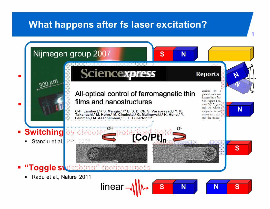
Switching by circularly polarized light Stanciu et al., PRL 2007
“Toggle switching” ferrimagnets Radu et al., Nature 2011
Nijmegen group 2007
[Co/Pt]n

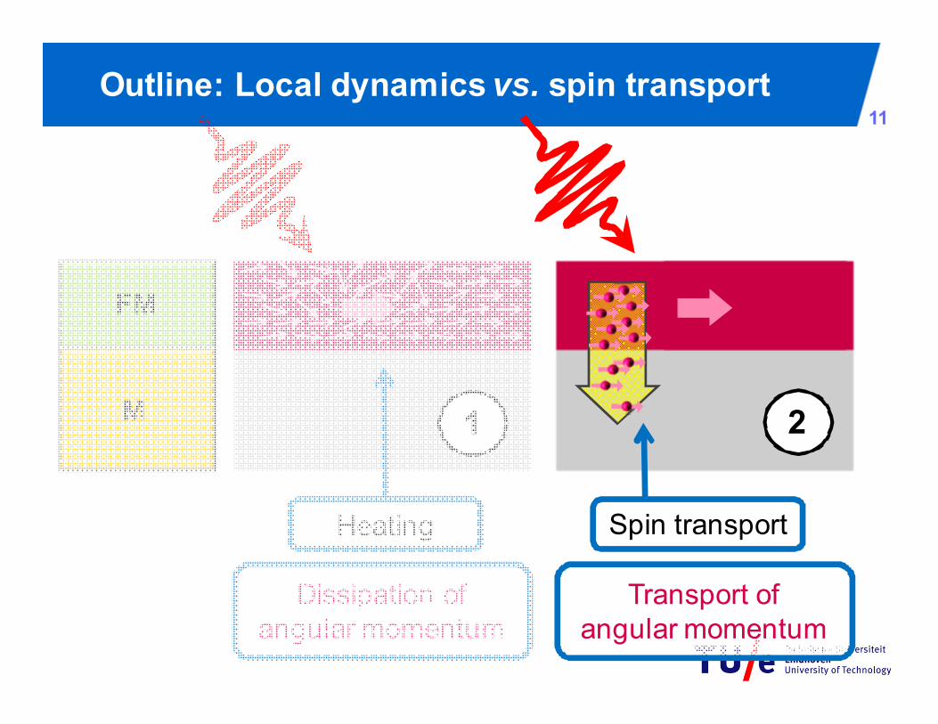
Outline: Local dynamics vs. spin transport2
FM
M
Heating Spin transport
1 2
Dissipation of angular momentum
Transport of angular momentum

Outline: Towards Integrated MagnetoPhotonics
Stanciu, Rasing et al., PRL 2007 Stanciu, Rasing et al., PRL 2007 Stanciu, Rasing et al., PRL 2007
Parkin et al.
3D ractetrack3

Essential ingredient: Fs loss of magnetization4
0.5
1.0
MO
con
trast
0 5 10 15
∆t (ps)
Ni thin film
50 fspump/probe
excited electronslaser pulse
electr. lattice
spins
Jean-Yves Bigot1956-2018
Eric Beaurepaire1959-2018
E. Beaurepaire, J.-C. Merle, A. Daunois, and J.-Y. Bigot., Phys. Rev. Lett. 76, 4250 (1996)
0 1 2300
400
500
0,8
0,9
1,0
Tem
pera
ture
(K)
Delay (ps)
E
M magnetization
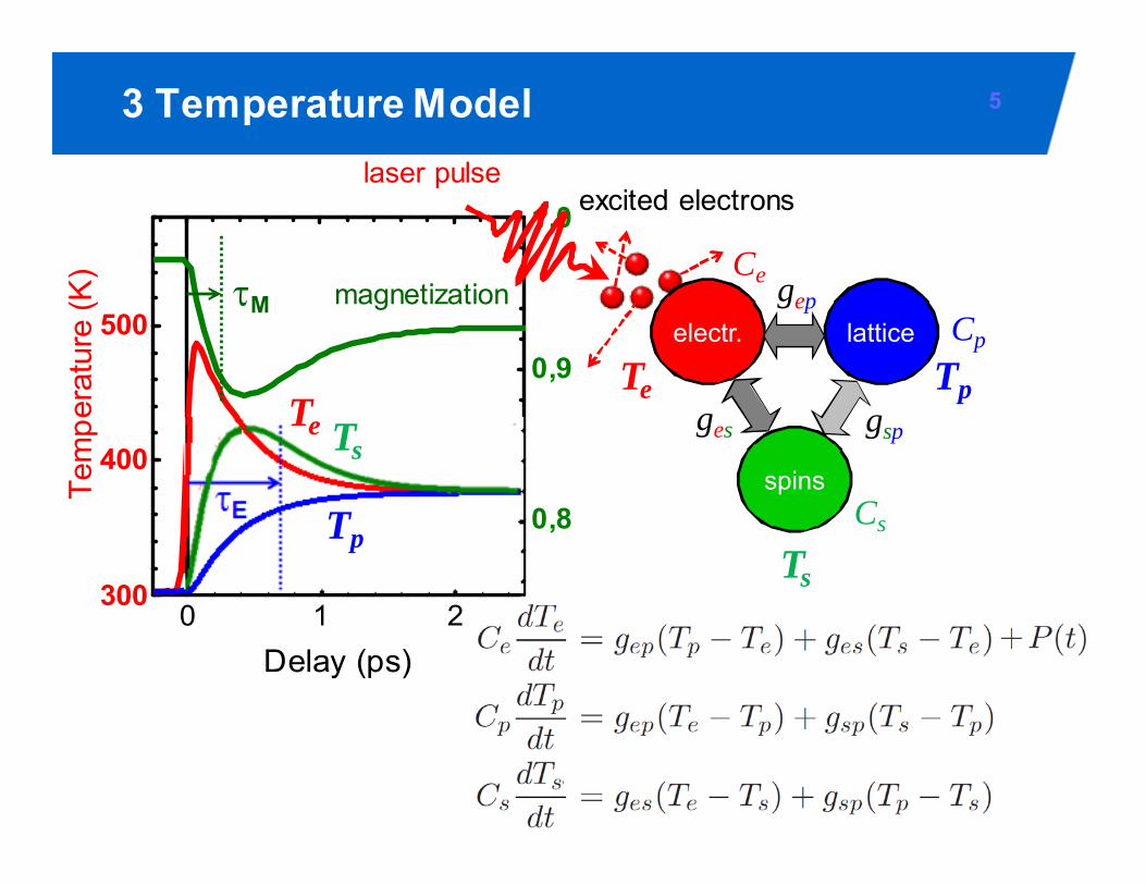
3 Temperature Model 5
excited electronslaser pulse
electr. lattice
spins
Te Tp
Ts
Cs
Ce
Cp
gep
gspgesTe
Tp
Ts

Different materials, different response6
0.5
1.0
MO
con
trast
0 5 10 15
∆t (ps)
Ni thin film
50 fspump/probe
E. Beaurepaire, J.-C. Merle, A. Daunois, and J.-Y. Bigot., Phys. Rev. Lett. 76, 4250 (1996)
-50 0 50 100 150
0,5
0,6
0,7
0,8
0,9
1,0
M /
M0
Delay (ps)
Nickel3d, Tc = 630 K, µat = 0.6 μB
50 ps0.2 ps
Wietstruk, Bovensiepen et al., Phys. Rev. Lett. (2011)
Weinelt(Tutorial)
Gadolinium4f, Tc = 295 K, µat = 7.5 μB

Claim: it’s just (non-equilibrium) thermodynamics
Photons and hot e- do not play a significant role…7
0 1 2 40,4
0,6
0,8
1,0
M /
M0
delay (ps)BK, Tobias Roth et al., Nature Mat. 2010
Cobalt 10 nm
Electron thermalization within 100 fs!
pump
MO probe
Direct heating
Indirect via hot electronsBergeard, Mangin, BK, Malinowski et al.,
Phys. Rev. Lett. 2016
Mangin(Tutorial),
Bokor
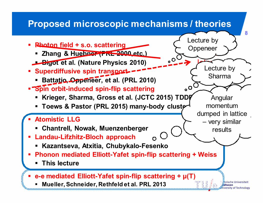
8Proposed microscopic mechanisms / theories
Photon field + s.o. scattering Zhang & Huebner (PRL 2000,etc.) Bigot et al. (Nature Physics 2010)
Superdiffusive spin transport Battatio, Oppeneer, et al. (PRL 2010)
Spin orbit-induced spin-flip scattering Krieger, Sharma, Gross et al. (JCTC 2015) TDDFT Toews & Pastor (PRL 2015) many-body cluster
Atomistic LLG Chantrell, Nowak, Muenzenberger
Landau-Lifzhitz-Bloch approach Kazantseva, Atxitia, Chubykalo-Fesenko
Phonon mediated Elliott-Yafet spin-flip scattering + Weiss This lecture
e-e mediated Elliott-Yafet spin-flip scattering + μ(T) Mueller, Schneider, Rethfeld et al. PRL 2013
discussedlater
Lecture byOppeneer
Lecture bySharma
Angularmomentum
dumped in lattice– very similar
results

9
e-e
Microscopic 3TM - Model Hamiltonian
e
eU
e
e e
e
peσ
e-σ
pasf
Assumption: τth ~ 0 Spin-flip upon momentum scattering (Elliott-Yafet)
Leading to: τE ~ 0.4 ps
Koopmans et al., PRL 2005, Nat. Mater. 2010
e-p e-p + spin flip
kTe
EEF
ex
+½
-½
(½ + n)hp
electrons spins phonons
Spin-less free electrons Debye or EinsteinMean field Weiss
Spintronics:2 2
0 026
Fsf
sf sf
val
10
12
2
ps 150 /
8 sfatatD
Cepsf a
VEkTg
aR
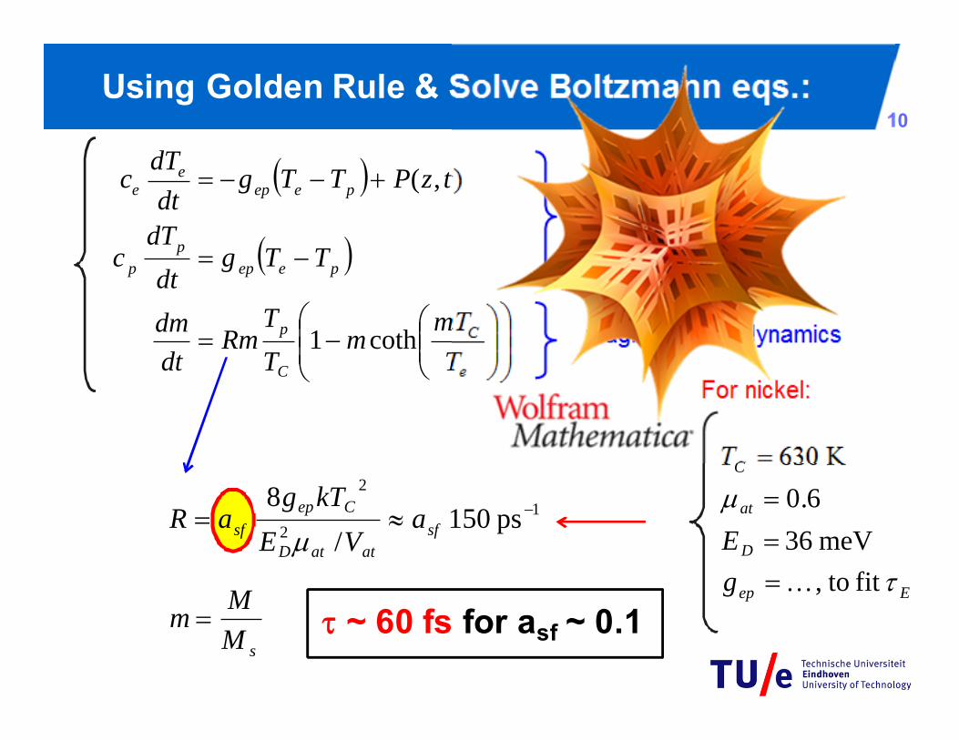
Using Golden Rule & Solve Boltzmann eqs.:
e
C
C
p
peepp
p
peepe
e
TmT
mTT
Rmdtdm
TTgdt
dTc
tzPTTgdtdT
c
coth1
),(
Eep
D
at
C
gE
T
fit to, meV 36
6.0K 630
For nickel:
sMMm
electron and lattice dynamics
magnetization dynamics
~ 60 fs for asf ~ 0.1
Outline: Local dynamics vs. spin transport11
FM
M
Heating Spin transport
1 2
Dissipation of angular momentum
Transport of angular momentum
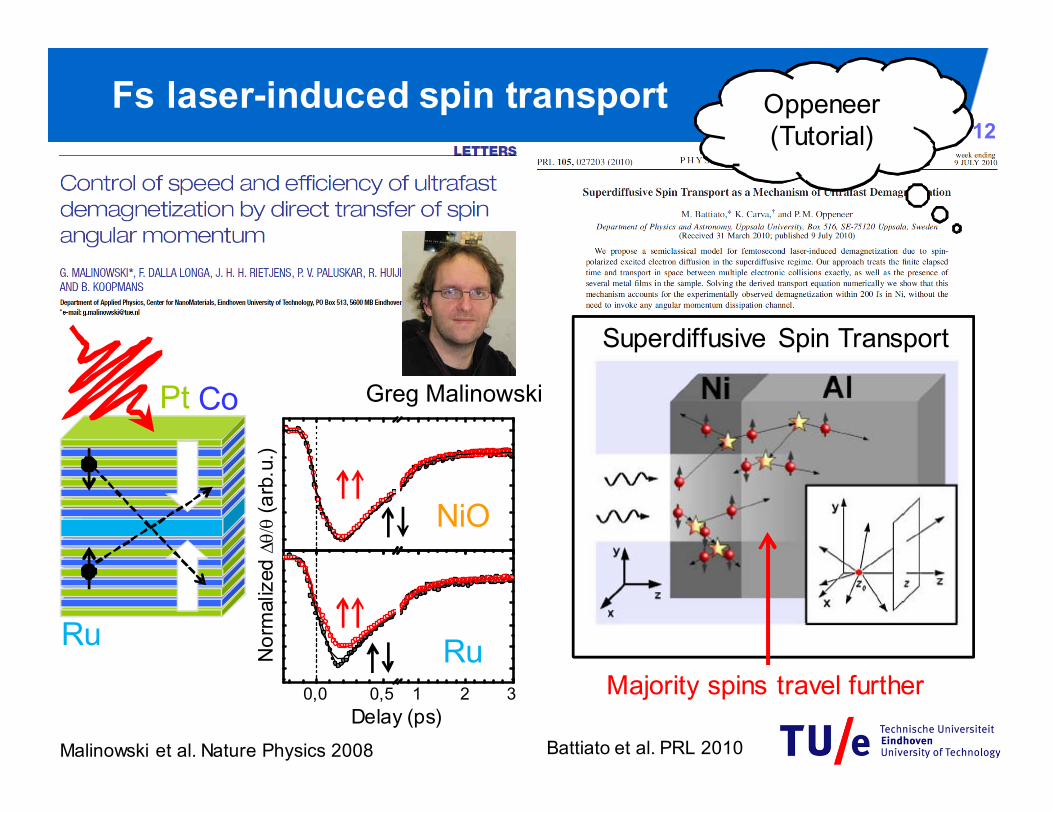
Fs laser-induced spin transport12
Malinowski et al. Nature Physics 2008
Ru
Pt Co
0,0 0,5 1 2 3
Nor
mal
ized
(arb
.u.)
Delay (ps)
Ru
NiO
Battiato et al. PRL 2010
Superdiffusive Spin Transport
Majority spins travel further
Greg Malinowski
Oppeneer(Tutorial)

Optical generation of fs spin currents13
EF
3d4sp
Ni Super-diffusiveMajority spin
maj. > min.
Spin-dependent Seebeck
T T
dT/dx
P Balistic
FM FM or NM
Due to:- Matrix elements- DOS- Transmission- Screening
P’
P’Spin dep. life time:
tup > tdown
So pure spin current!
Battiato, Oppeneer et al., PRL 2010
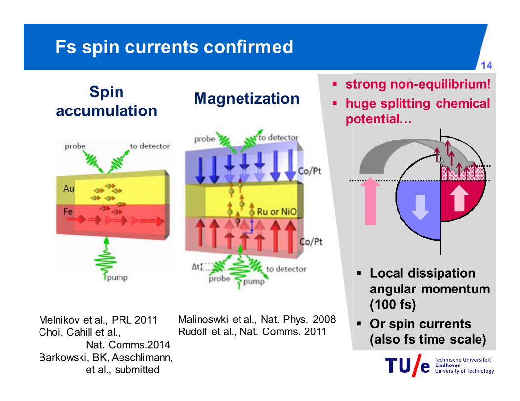
Fs spin currents confirmed14
Spinaccumulation
Magnetization
Malinoswki et al., Nat. Phys. 2008Rudolf et al., Nat. Comms. 2011
strong non-equilibrium! huge splitting chemical
potential…
Local dissipation angular momentum (100 fs)
Or spin currents (also fs time scale)
Melnikov et al., PRL 2011Choi, Cahill et al.,
Nat. Comms.2014Barkowski, BK, Aeschlimann,
et al., submitted
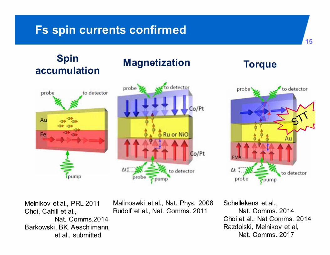
Fs spin currents confirmed15
Spinaccumulation Torque
Schellekens et al., Nat. Comms. 2014
Choi et al., Nat Comms. 2014Razdolski, Melnikov et al,
Nat. Comms. 2017
Magnetization
Malinoswki et al., Nat. Phys. 2008Rudolf et al., Nat. Comms. 2011
Melnikov et al., PRL 2011Choi, Cahill et al.,
Nat. Comms.2014Barkowski, BK, Aeschlimann,
et al., submitted

in-plane
PMA
Experimental demonstration Optical STT16
in-plane
PMA
Co
Cu
[Co/Ni]n
HK
HK
Schellekens, BK et al., Nature Comms. 2014See also: Choi, Lee et al., Nature Comms. 2014
Polar MOKEmeasuring Mz
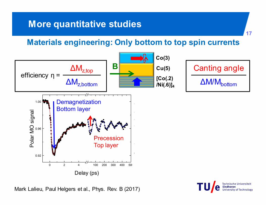
More quantitative studies
Materials engineering: Only bottom to top spin currents17
∆M / M of Bottom layer (%)Delay (ps)
Can
ting
angl
e(m
deg.
)
Pol
arM
O s
igna
l
Co(3)
Cu(5)
[Co(.2)/Ni(.6)]4
DemagnetizationBottom layer
PrecessionTop layer
Mark Lalieu, Paul Helgers et al., Phys. Rev. B (2017)
efficiency η = ∆Mz,top
∆Mz,bottom
B
z
y±0.08o
±0.4o
Canting angle
∆M/Mbottom
How is spin current generated?18
0 1 2 3 4 5 60
5
10
Effic
ienc
y,
(%)
Repeats0 1 2 3 4 5 6
0
5
10
15
20
25
30
Can
ting
angl
e (m
deg.
/ %
)
Ni equiv. thickness (nm)
Transfered spinproportional with thickness!
~ Thickness
Co(3)
Cu(5)
[Co(.2)/Ni(.6)]N/Co(.2)N = 1 N = 2
N = 3N = 4
?N = 2
N = 1
N = 3
N = 4?
N = 1 23 4
Helpful in idenmtifyingmechanism!
Mark Lalieu, Paul Helgers et al., Phys. Rev. B (2017)

How is transverse momentum absorbed?19
0 1 2 3 4 5 6 70
1
2
3
4
(%
)
Thickness (nm)0 2 4 6 8
0
10
20
30
Can
ting
angl
e (m
deg.
/ %
)
Thickness (nm)
Co Variable Thickness
Cu(5)[Co(.2)/Ni(.6)]4
Pt(2)
90% absorbed in 1.5 nm
~ 1 / Thickness
See also Razdolski, Melnikov et al., Nature Comms. 2017
Mark Lalieu, Paul Helgers et al., Phys. Rev. B (2017)
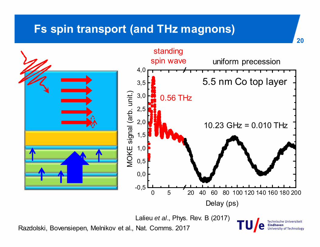
Fs spin transport (and THz magnons)20
Razdolski, Bovensiepen, Melnikov et al., Nat. Comms. 2017
10.23 GHz = 0.010 THz
0.56 THz
5.5 nm Co top layer
0 5 20 40 60 80 100 120 140 160 180 200-0,5
0,0
0,5
1,0
1,5
2,0
2,5
3,0
3,5
4,0
MO
KE
sig
nal (
arb.
uni
t.)
Delay (ps)
uniform precessionstanding
spin wave
Lalieu et al., Phys. Rev. B (2017)

Resolving dispersion & q-dependent damping
? ~ 1/t2 ~ q2
Mark Lalieu, preprint

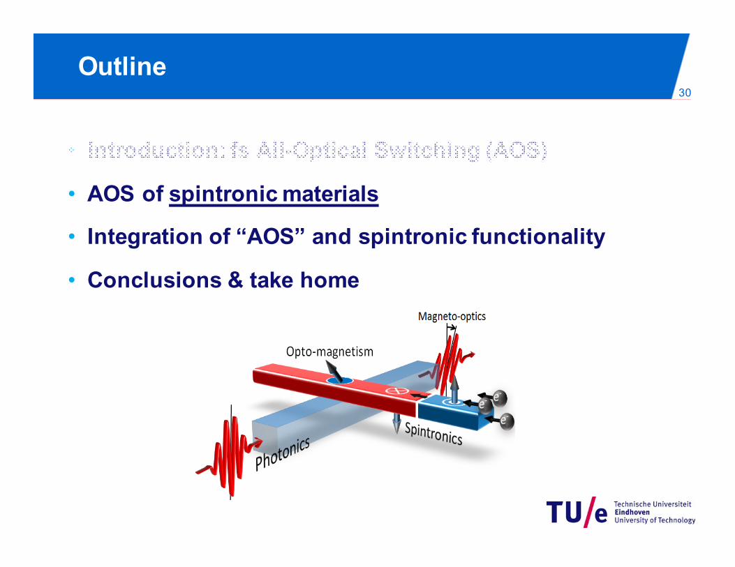
Outline
• Introduction: fs All-Optical Switching (AOS)
• AOS of spintronic materials
• Integration of “AOS” and spintronic functionality
• Conclusions & take home
22
3
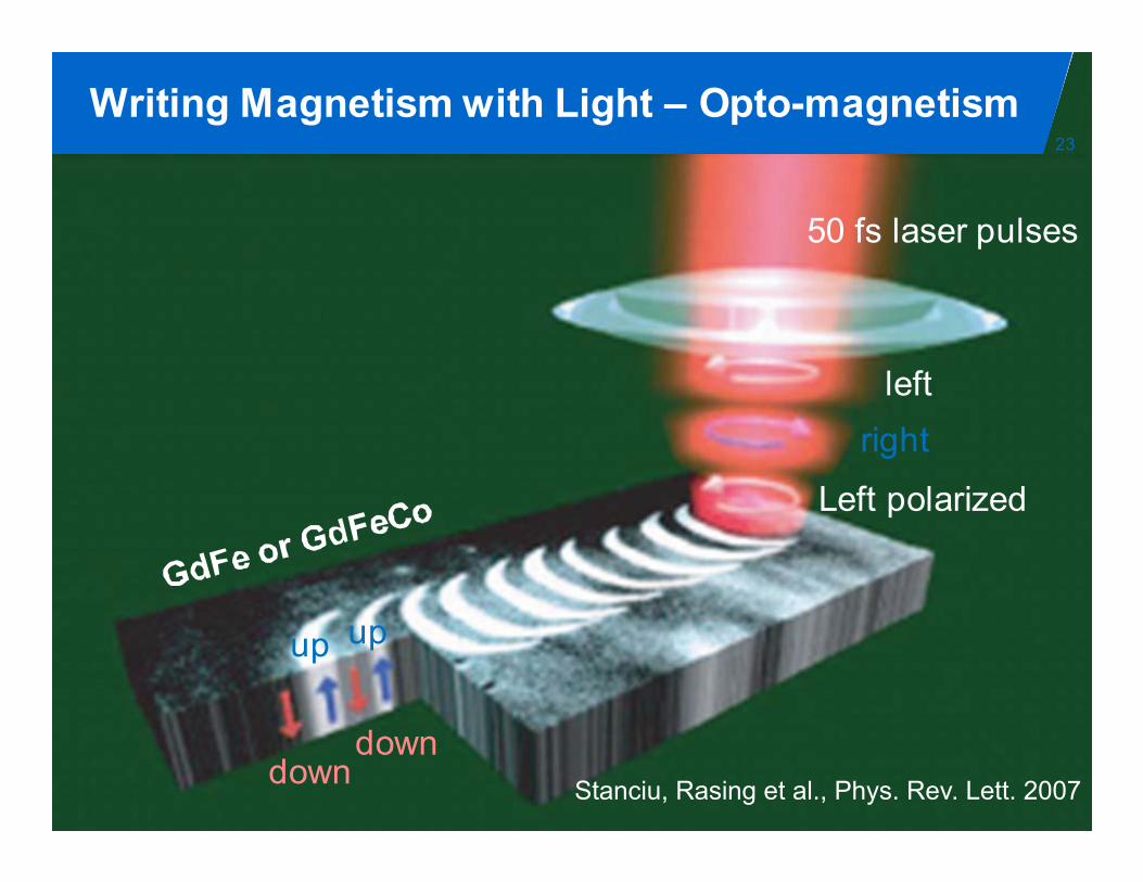
Writing Magnetism with Light – Opto-magnetism23
Stanciu, Rasing et al., Phys. Rev. Lett. 2007
50 fs laser pulses
leftright
Left polarized
up
down
up
down

Writing Magnetism with Light – Opto-magnetism24
Stanciu, Rasing et al., Phys. Rev. Lett. 2007
50 fs laser pulses
leftright
Left polarized
up
down
up
down
Ostler et al., Nature Comms. 2012
20 µm
Toggle mechanism (linearly polarized!)
Khorsand et al., Phys. Rev. Lett. 2012
Helicity dependence just due to circular dichroism
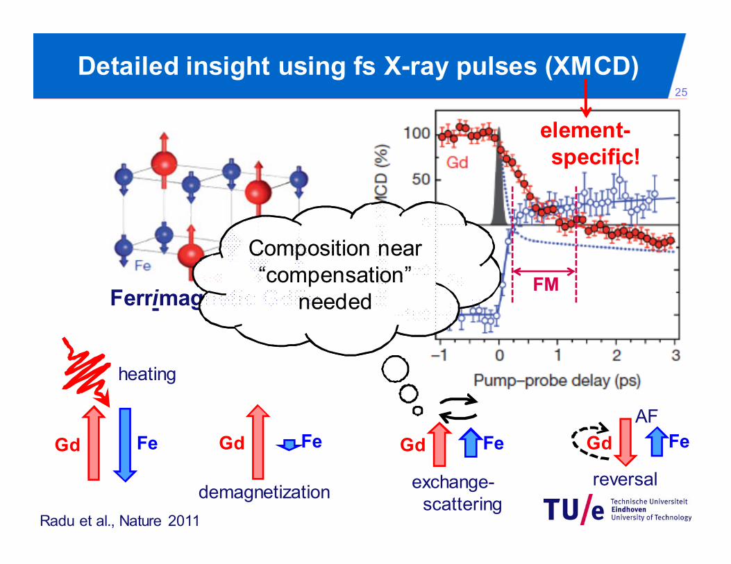
Detailed insight using fs X-ray pulses (XMCD)25
Radu et al., Nature 2011
Ferrimagnetic GdFe
element-specific!
FeGd
heating
FeGd
demagnetization
FeGd
exchange-scattering
FeGd
reversal
AF
FM
Composition near “compensation”
needed
Composition near “compensation”
needed
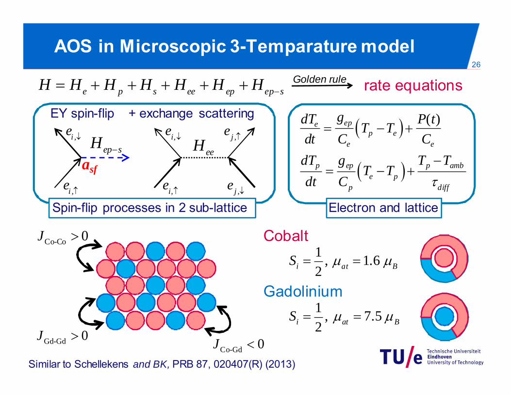
AOS in Microscopic 3-Temparature model26
,ie
asf
,ie
,ie
,ie ,je
,je
1 , 1.6 2i at BS
Co-Co 0J Cobalt
Gadolinium1 , 7.5 2i at BS
( )epep e
e e
p ep p ambe p
p diff
gdT P tT Tdt C CdT g T T
T Tdt C
Electron and lattice
EY spin-flip + exchange scattering
Spin-flip processes in 2 sub-lattice
Similar to Schellekens and BK, PRB 87, 020407(R) (2013)Co-Gd 0J Gd-Gd 0J
e p s ee ep ep sH H H H H H H rate equationsGolden rule
eeHep sH

AOS phase diagram for CoxGd1-x27
M =
0 @
RT
switch
no-switch
Maarten Beens et al., in preparation
+1
0
-1
Co
Gd
0 1 2∆t (ps)
Concentration Co
+1
0
-1
Co
Gd
0 1 2∆t (ps)
P0
(108
Jm-3
)
+1
0
-1
Co
Gd
0 1 2∆t (ps)
+1
0
-1
Co
Gd
0 1 2∆t (ps)
τdiff = 2 ps

Requirements AOS vs. Fast CI-DWM
1. Anti-parallel sub-lattices = reduced M
2. Different (EY) demagnetization times
3. Exchange scattering4. PMA (useful)
28
1. Anti-parallel sub-lattices = reduced Me in white ink
2. Strong SOC SHE3. Strong SOC DMI and
so forth4. PMA
Yang, Parkin et al., Nature Nanotechnol. (2015)
(M1 – M2) / MsVe
loci
ty(m
s-1
)M1
M2
DMIPtCo
SHE
700 m/s
PMA
()

Our dream: Spintronic Photonic Memory29
• If we can engineer the proper magnetic stack
291000 m/s50 nm bits= 20 GHz
1000 m/s50 nm bits= 20 GHz
Outline
• Introduction: fs All-Optical Switching (AOS)
• AOS of spintronic materials
• Integration of “AOS” and spintronic functionality
• Conclusions & take home
30
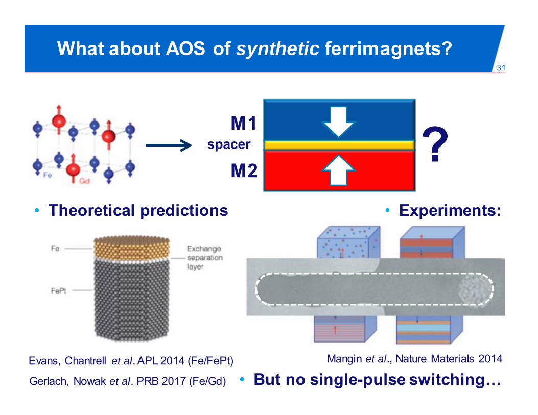
What about AOS of synthetic ferrimagnets?
• Theoretical predictions
31
M1
M2spacer ?
• Experiments:
Evans, Chantrell et al. APL 2014 (Fe/FePt)
• But no single-pulse switching…Mangin et al., Nature Materials 2014
Gerlach, Nowak et al. PRB 2017 (Fe/Gd)
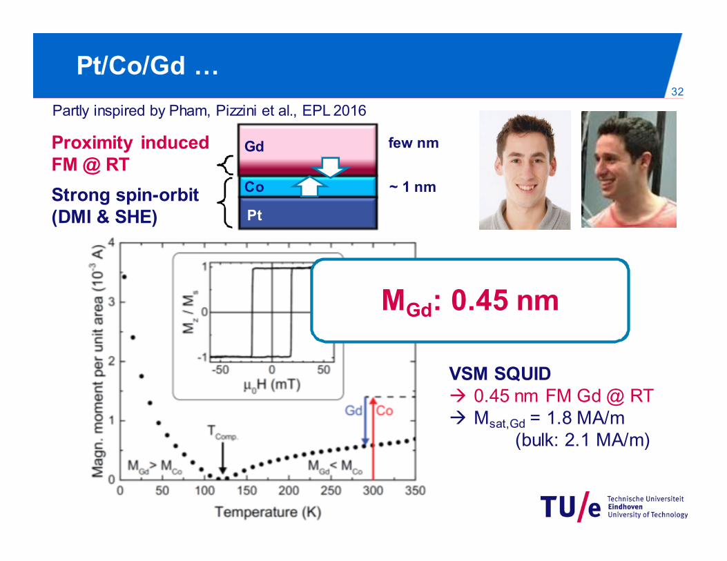
Pt/Co/Gd … 32
Proximity induced FM @ RT
Co
Gd
Pt
few nm
~ 1 nmStrong spin-orbit(DMI & SHE)
Partly inspired by Pham, Pizzini et al., EPL 2016
VSM SQUID 0.45 nm FM Gd @ RT Msat,Gd = 1.8 MA/m
(bulk: 2.1 MA/m)
MGd: 0.45 nm
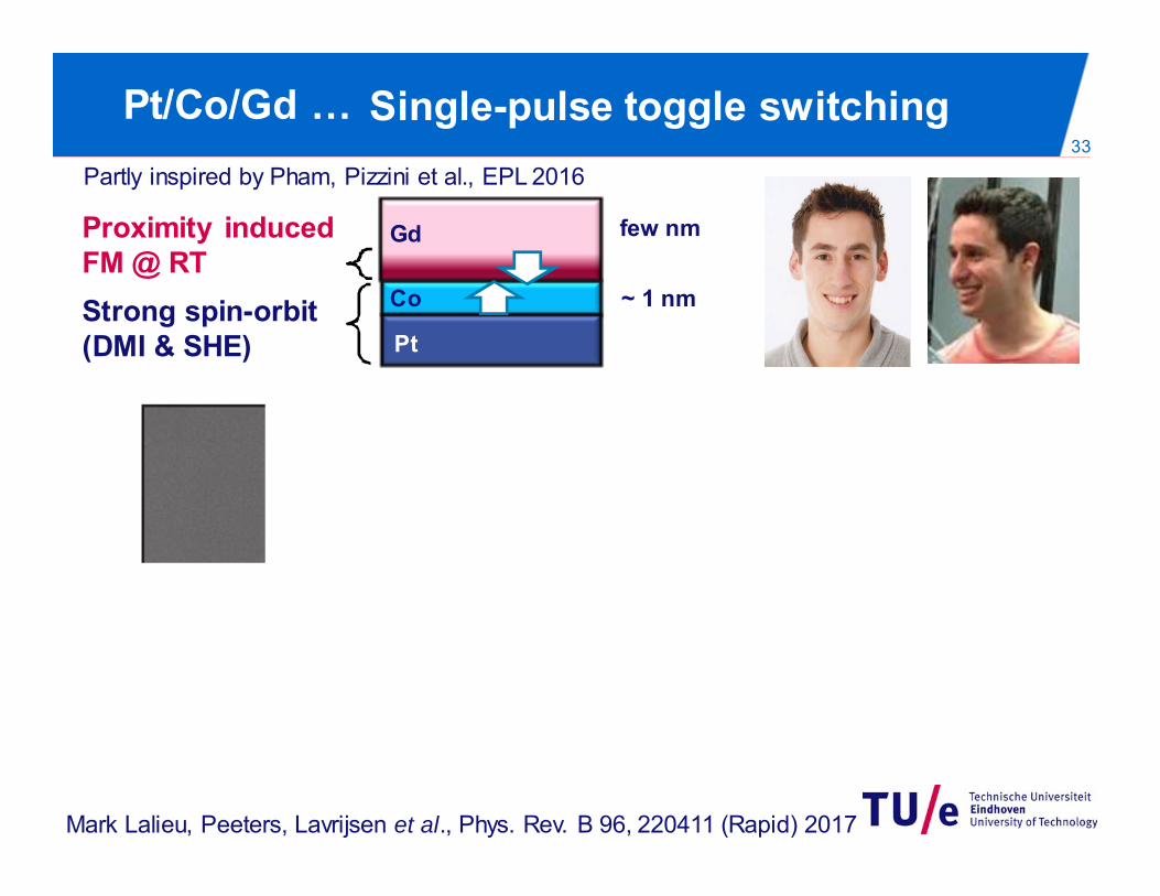
Pt/Co/Gd … 33
Mark Lalieu, Peeters, Lavrijsen et al., Phys. Rev. B 96, 220411 (Rapid) 2017
Single-pulse toggle switching
Proximity induced FM @ RT
Co
Gd
Pt
few nm
~ 1 nmStrong spin-orbit(DMI & SHE)
Partly inspired by Pham, Pizzini et al., EPL 2016
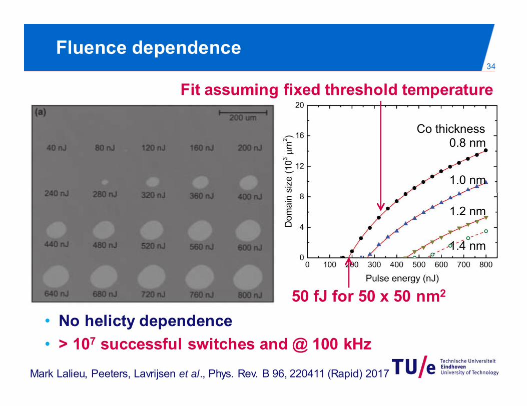
Fluence dependence
50 fJ for 50 x 50 nm2
34
Mark Lalieu, Peeters, Lavrijsen et al., Phys. Rev. B 96, 220411 (Rapid) 2017
• No helicty dependence• > 107 successful switches and @ 100 kHz
Fit assuming fixed threshold temperature
Co thickness0.8 nm
1.0 nm
1.2 nm
1.4 nm

Switching far from compensation point
• How come?
35Alloys:
Composition near “compensation”
needed
Alloys:Composition near “compensation”
needed
Co
Gd
Pt[Co/Ni]n
Gd
Pt
Co [Co/Ni]n
6
5
4
3
n = 2
Mark Lalieu, Maarten Beens et al., in preparation

Layered multi-sublattice M3TM36
( )epep e
e e
p ep p ambe p
p diff
gdT P tT T
dt C CdT g T T
T Tdt C
,ie
asf
,ie
,ie
,ie ,je
,je
1, 1.6
2i at BS , , 0i i i jJ J
, , 0i i i jJ J
Cobalt
Gadolinium
1 , 7.5 2i at BS
1234567
i
, , 0i i i jJ J
Electron and lattice
EY spin-flip + exchange scattering
slab-wise M3TM
Mark Lalieu, Maarten Beens et al., in preparation

AOS of alloy versus bi-layer37
• How come?
M =
0 @
RY
Alloy Bi-layer
switch
no-switch
switch
no-switch
Mark Lalieu, Maarten Beens et al., in preparationEffective medium
3 Gd layers
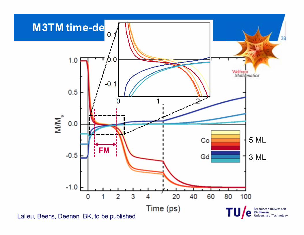
M3TM time-dependence38
Lalieu, Beens, Deenen, BK, to be published
5 ML
3 MLFM

Outline
• Introduction: fs All-Optical Switching (AOS)
• AOS of spintronic materials
• Integration of “AOS” and spintronic functionality
• Conclusions & take home
39

Current (SHE) induced motion in Pt/Co/Gd
500 ns pulses0.4 x 1012 A/m2
vDW = 8 m/s
1 μm wide Pt/Co/GdMagnetic racetrack
Lalieu, Lavrijsen and BK, arXiv 1809.02347
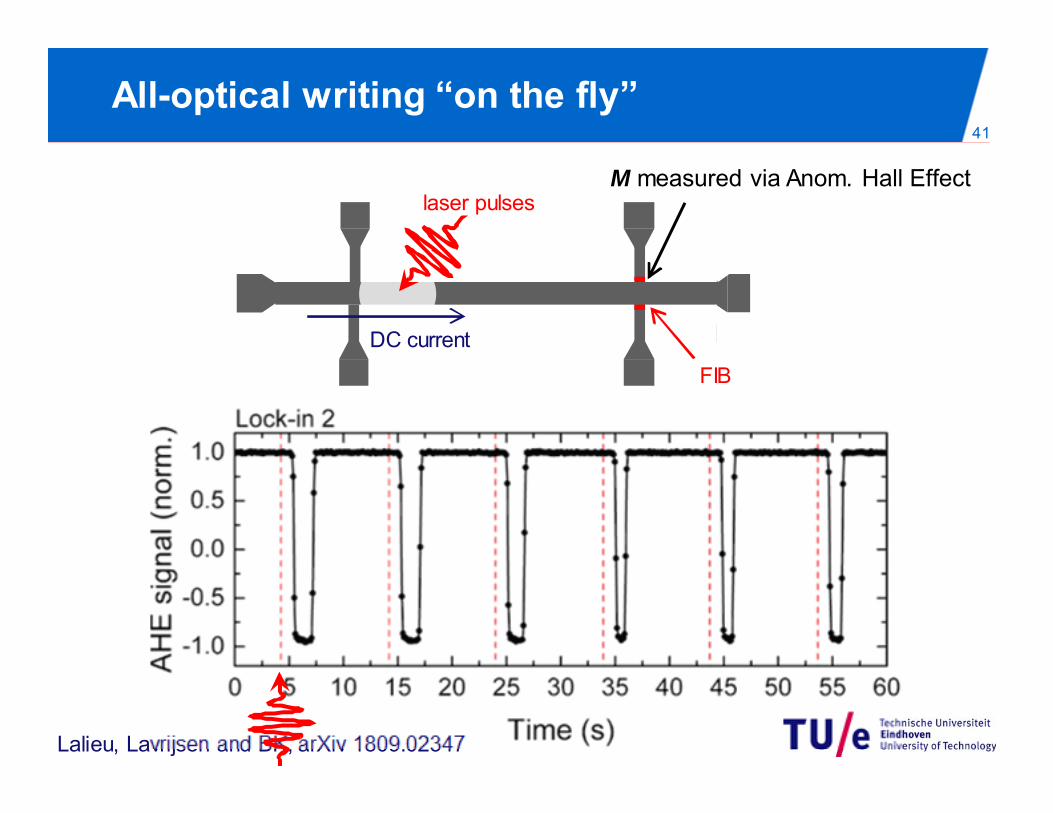
Lalieu, Lavrijsen and BK, arXiv 1809.02347
All-optical writing “on the fly”41
laser pulses
DC current
M measured via Anom. Hall Effect
FIB
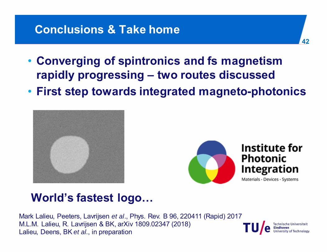
Conclusions & Take home
• Converging of spintronics and fs magnetism rapidly progressing – two routes discussed
• First step towards integrated magneto-photonics
42
World’s fastest logo…Mark Lalieu, Peeters, Lavrijsen et al., Phys. Rev. B 96, 220411 (Rapid) 2017M.L.M. Lalieu, R. Lavrijsen & BK, arXiv 1809.02347 (2018)Lalieu, Deens, BK et al., in preparation

Acknowledgements43