turn a highly-reflective metal into an omnidirectional
TRANSCRIPT

Progress In Electromagnetics Research, Vol. 134, 95–109, 2013
TURN A HIGHLY-REFLECTIVE METAL INTO ANOMNIDIRECTIONAL BROADBAND ABSORBER BYCOATING A PURELY-DIELECTRIC THIN LAYER OFGRATING
Feng Zhang1, †, Liu Yang1, 2, †, Yi Jin1, and Sailing He1, 2, *
1Centre for Optical and Electromagnetic Research, JORCEP, ZhejiangProvincial Key Laboratory for Sensing Technologies, ZhejiangUniversity, Hangzhou 310058, China2ZJU-SCNU Joint Research Center of Photonics, South China NormalUniversity, Guangzhou 510006, China
Abstract—We show that a metal can be turned into a broadbandand omnidirectional absorber by coating a purely-dielectric thin layerof grating. An optimal design for such an absorber is proposed byputting a dielectric slot waveguide grating (SWG) on the metallicsubstrate. The SWG consists of two germanium nanowires (Ge NWs)separated by a sub-100 nm slot in each period. Average absorptionreaches 90% when the incident angle varies between 0◦ and 80◦over a broad wavelength range from 300 nm to 1400 nm. Multipleoptical mechanisms/effects, namely, diffraction, waveguiding in thehigh-index Ge NWs and low-index air slot, Fabry-Perot resonancesas well as surface plasmon polaritons (SPPs), are identified to governthe absorption characteristics of the present absorber. The designedabsorber with such a dielectric grating is easier to fabricate ascompared with other absorbers with metallic nanostructures, and haspotential applications in, e.g., solar cells and photodetectors.
1. INTRODUCTION
Perfect absorption of light without any reflection or transmissionis of critical importance for optical energy conversion, especially invisible and near-infrared regime covering the main solar spectrum. Inorder to efficiently convert solar energy into electrical (or thermal)
Received 28 October 2012, Accepted 15 November 2012, Scheduled 21 November 2012* Corresponding author: Sailing He ([email protected]).† Feng Zhang and Liu Yang contributed equally to this work.

96 Zhang et al.
energy, which people can use directly, broadband perfect absorbersare required to harvest and absorb as many photons as possible [1–3]. Recent advances in micro-/nano-technology become helpful toachieve many flexible designs of broadband perfect absorbers basedon micro-/nano-structures [2, 4]. Metallic nanostructures supportingsurface plasmon polaritons (SPPs) are most widely employed due totheir strong ability to harvest and localize photons in a subwavelengthregion [2, 5, 6], where the resonant photons can be strongly absorbed bythe compositional metallic and/or lossy dielectric material. Recently,another interesting absorber, based on metallic metamaterials, hasbeen suggested [7]. Unlike plasmonic absorbers, both electric andmagnetic resonances can be excited simultaneously in the metamaterialabsorbers and complete absorption can be achieved [4, 8, 9]. However,the bandwidth is usually very narrow, due to the resonantcharacteristics [10–16]. By simply mixing together different resonatorswith different resonant frequencies, broad absorption spectrum canbe achieved [17–22]. Very recently, Søndergaard et al. proposed anon-resonant broadband absorber based on ultra-sharp convex groovesvia adiabatic nanofocusing of gap SPPs [23]. Another non-resonantabsorbers proposed by Cui et al. was made of a sawtoothed anisotropicmetamaterial via slowlight modes and a large bandwidth of about 86%of its central wavelength was achieved [24] (experimental verificationin the microwave regime can be found in Ref. [25]). Low-bandgapsemiconductors themselves are also good broadband absorbers, e.g.,Si, Ge, and will have much better antireflection and absorptionproperties if micro-/nano-structures are formed, e.g., microwires [26],nanowires/holes [27–29], nanotips [30], nanocones [31], etc. A hybriddielectric-metal core-shell grating structure over a metallic substratewas used in Ref. [32] to achieve broadband, omnidirectional, andpolarization-independent absorption by combining two kinds of opticalmodes, namely, Bloch and SPP modes.
In the present paper we report a novel absorption structure bysimply putting a purely-dielectric thin layer of grating on a metallicsubstrate. We will also show that by combining multiple physicaleffects together, an enhanced absorption and ultrabroad bandwidth canbe achieved. Our optimal structure consists of a gold (Au) substratecovered with a dielectric Slot Waveguide Grating (SWG, dielectricgrooves are much easier to fabricate than metallic grooves [23]), whichcontains two Ge nanowires (NWs) with a small separation betweenthem in each period. Compared with a grating structure with onlyone NW in each period, our SWG-based structure has a flatter totalabsorption spectrum over a broad wavelength range from 300 to1400 nm and is also angle-insensitive (from 0 to 80◦).

Progress In Electromagnetics Research, Vol. 134, 2013 97
2. STRUCTURE AND THEORETICAL MODEL
Our proposed SWG based absorber is shown schematically inFigure 1(a), where there are two Ge NWs separated by d in eachperiod on a gold (Au) substrate. Compared with silicon (Si) oftenused in the solar cell industry, Ge is more expensive. However, Ge hasa much higher absorption coefficient over a much broader wavelengthrange than Si. On the other hand, Ge is also a solar material oftenused in multi-junction thin-film solar cells to absorb photons in thenear-infrared wavelength range [33]. Thus we choose Ge instead ofSi as the main absorbing material. In the nanostructure shown inFigure 1(a), the Ge NW widths are set equal, i.e., w1 = w2, unlessotherwise specified. The grating height is set to h. As a reflector, theAu substrate is assumed to be thick enough to prevent any transmissionthrough it. Due to the rather small separation between the two NWsin each period, slot waveguide modes together with some interestingoptical responses can be generated in our structure. In order to focuson the analysis on these effects, we fix the grating period to 620 nm,i.e., P = 620 nm, throughout the paper. For comparison, a gratingwith only one NW of width, w, in each period is plotted in Figure 1(b)with the same period, P = 620 nm, and NW height, h.
We employed the finite element method (FEM) [34] to simulate theoptical responses when a plane wave is incident from the top with anincident angle, θ, and a wave vector, k0, as shown in Figure 1. The lightwavelength, λ, is chosen from 300 to 1500 nm, beyond which Ge haslittle absorption. Here, only transverse-magnetic (TM) polarizationis considered with magnetic field, H, perpendicular to the x-z plane
(a) (b)
Figure 1. Schematic diagram of (a) an SWG-based absorber withtwo NWs in each period; (b) an absorber with only one NW in eachperiod. A TM-polarized plane wave is incident from the top with anincident angle, θ, and a wave vector, k0. The inset of Figure 1(b) showsdielectric constant (n− i · k) of Ge [35].

98 Zhang et al.
in order to excite the polarization-sensitive slot waveguide and SPPmodes, and investigate their effects on the optical performances. In thesimulation, the dielectric constant of Ge and Au are both chosen frompreviously published experimental data [35]. The former is shown inthe inset of Figure 1(b). Through numerical simulation, we can easilyget the electric field distribution, E, as well as the partial absorptionsin each of the compositional material, AGe and AAu from the followingequation:
AGe orAu =
∫∫GeorAu
πcλ · Im (εGe or Au) |E|2 dxdz
Source power(1)
where Im(ε) is the imaginary part of the material’s dielectric constant.Since there is no other absorbing materials in our structure, the totalabsorption can be calculated by A = AGe + AAu. In comparison,A = 1 − R is not a good way to calculate the total absorption.Since there are many optical mechanisms/effects to be excited withinthis structure, including diffraction (Rayleigh anomalies), waveguidingin the high-index Ge NWs and low-index air slot, Fabry-Perot (FP)resonances and SPPs, if the reflection is monitored far from the topGe NWs, some near-field optical behaviors cannot be detected withA = 1 − R and the result may become quite different from thatcalculated by A = AGe + AAu, unless the reflection monitor is setvery close to the top Ge NWs. In order to eliminate the possiblecalculation errors, we calculate the absorption by using A = AGe+AAu
in this paper. This way the structural effects (including the NW width,height, filling ratio, etc.) on the partial absorptions, AGe and AAu, andconsequently the total absorption, A, can also be studied (see the nextsection).
3. SIMULATION RESULTS AND DISCUSSION
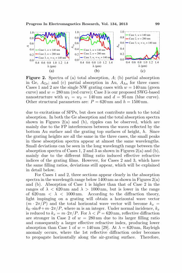
Figures 2(a), (b) and (c) show the spectra of total absorption, A, andthe partial absorption, AGe and AAu, respectively for the single NWgrating absorbers with NW widths of 140 nm (green curve) and 280 nm(red curve), and our SWG-based absorber with w1 = w2 = 140 nm andd = 95 nm (blue curve). We refer these three structures as Case 1,Case 2, and Case 3, respectively for easy description. From Figure 2,it is shown that for all the three cases the absorption in Ge dominatesthe total absorption in the wavelength range below 1400 nm and thereare sharp drops around 1400 nm, beyond which the absorption of Geindicated by the imaginary part of its refractive index is at least oneorder of magnitude smaller [35]. Here absorption in Au becomes larger
Progress In Electromagnetics Research, Vol. 134, 2013 99
Ge
Au
0.4 0.6 0.8 1.0 1.2 1.4
λ (µm)
1.0
0.4
0.6
0.8
0.2
0.0
A
Case 1, w = 140 nm
Case 2, w = 280 nm
Case 3, w = w = 140 nm1 2
Case 1, w = 140 nm
Case 2, w = 280 nm
Case 3, w = w = 140 nm1 2
Case 1, w = 140 nm
Case 2, w = 280 nm
Case 3, w = w = 140 nm1 2
0.4 0.6 0.8 1.0 1.2 1.4
λ (µm)
0.4 0.6 0.8 1.0 1.2 1.4
λ (µm)
1.0
0.4
0.6
0.8
0.2
0.0
A
1.0
0.4
0.6
0.8
0.2
0.0
A
(a) (b) (c)
Figure 2. Spectra of (a) total absorption, A; (b) partial absorptionin Ge, AGe; and (c) partial absorption in Au, AAu for three cases:Cases 1 and 2 are the single NW grating cases with w = 140 nm (greencurve) and w = 280 nm (red curve); Case 3 is our proposed SWG-basednanostructure with w1 = w2 = 140 nm and d = 95 nm (blue curve).Other structural parameters are: P = 620 nm and h = 1500 nm.
due to excitations of SPPs, but does not contribute much to the totalabsorption. In both the Ge absorption and the total absorption spectrashown in Figures 2(a) and (b), ripples can be observed, which aremainly due to the FP interferences between the waves reflected by thebottom Au surface and the grating top surfaces of height, h. Sincethe grating heights are all the same in the three cases, the small peaksin these absorption spectra appear at almost the same wavelengths.Small deviations can be seen in the long wavelength range between theabsorption spectra of Cases 1, 2 and 3 as shown in Figures 2(a) and (b),mainly due to the different filling ratio induced effective refractiveindices of the grating films. However, for Cases 2 and 3, which havethe same filling ratios, deviations still appear, which will be explainedin detail below.
For Cases 1 and 2, three sections appear clearly in the absorptionspectra in the wavelength range below 1400 nm as shown in Figures 2(a)and (b). Absorption of Case 1 is higher than that of Case 2 in theranges of λ < 620 nm and λ > 1000 nm, but is lower in the rangeof 620 nm < λ < 1000 nm. According to the diffraction theory,light impinging on a grating will obtain a horizontal wave vector(m · 2π/P ) and the total horizontal wave vector will become kx =k0 ·sin θ+m ·2π/P , where m is an integer. Under normal incidence, kx
is reduced to kx = m ·2π/P . For λ < P = 620 nm, reflective diffractionare stronger in Case 2 of w = 280 nm due to its larger filling ratioand consequently a larger effective refractive index, producing lowerabsorption than Case 1 of w = 140 nm [29]. At λ = 620 nm, Rayleighanomaly occurs, where the 1st reflective diffraction order becomesto propagate horizontally along the air-grating surface. Therefore,

100 Zhang et al.
absorption increases in Case 2 but decreases in Case 1 where thelight experiences less absorbing material as shown in Figures 2(a)and (b). According to the phase-matching condition for the refractivediffractions, that is, kx = [k0 ·(1−w/P )+k0nGe ·w/P ]·sin θ′m, where θ′mis the refractive diffraction angle of mth diffraction order. For Case 1,the 1st refractive diffraction order becomes another Rayleigh anomalyat λ = 1096 nm and will propagate horizontally along x directionwith θ′m = 90◦. For Case 2, Rayleigh anomaly of the 2nd refractivediffraction order occurs at λ = 822 nm. For the wavelengths beyondeach Rayleigh anomaly, the energy will be redistributed between theremaining diffraction orders, namely, 0-order for Case 1 and 0- and 1-orders for Case 2, of which the 0-order diffraction obtains more energy.Then the FP resonances in the z direction dominate the absorptionspectra. In the wavelength range beyond 1000 nm, we find that SPPsare excited at the bottom interface between Ge NW and Au with oneand three magnetic field maxima respectively for Cases 1 and 2 asshown in Figures 3(a) and (b). Since the magnetic fields of SPPs areconcentrated in the similar way in this wavelength range, only one
(a) (b) (c)
(g)
(d) (f)(e)
Figure 3. Magnetic field distributions at λ = 1230 nm: amplitude(|Hy|, top row) and phase (ϕHy, bottom row) for three cases: (a), (d)Case 1, (b), (e) Case 2 and (c), (f) Case 3. The structural parametersfor each case are the same as those in Figure 2. (g) Electric fileddistribution, |E|, at λ = 1230 nm for Case 3.

Progress In Electromagnetics Research, Vol. 134, 2013 101
example at λ = 1230 nm is shown in Figure 3 for all three cases forcomparison. For Case 1, the 140 nm-wide Ge NWs (as waveguides) arenarrow enough to confine light of long wavelengths as considered hereeven though most magnetic field is well confined in them as shown inFigure 3(a). Usually wider Ge NWs, e.g., Case 2 with twice widthof NW in Case 1, are thought to have much stronger confinement oflight than narrower ones. However, the magnetic field in Figure 3(b)shows that much more light is leaking out of the wider (280 nm-wide)NW compared with that of Case 1 in Figure 3(a). From the phasedistribution of Case 2 shown in Figure 3(e), it is clearly seen thatthe phase changes twice along the x direction within the Ge NW,which evolves gradually from the bottom phase induced by the excitedhigher-order SPP mode at the surface of the Au substrate. Such aphase change along the x direction makes the wider NW worse in lightconfinement than the narrower half-width NW. In contrary, withoutany significant phase changes, the phase distribution of Case 1 shownin Figure 3(d) is favorable for a better confinement for photons of longwavelengths shown in Figure 3(a), resulting in better absorptions thanCase 2 in this wavelength range as shown in Figures 2(a) and (b).
Interestingly, by introducing a slot into the 280 nm-wide NW ineach period, an ultra-broadband absorption spectrum can be achievedfor our proposed absorber of Case 3 with the merits of both Cases 1and 2 as shown in Figures 2(a) and (b). In the short wavelength rangebelow 1000 nm, stronger scattering is generated by the two NWs in eachperiod in Case 3, where the 1st refractive diffraction order experiencesmore changes of index in comparison with Case 2 of one 280 nm-wide NW in each period, and experiences more absorbing materialsin comparison with Case 1 of one 140 nm-wide NWs in each period.Therefore, the absorption spectrum becomes flatter with absorptioncomparable to that of Case 1 at λ < 620 nm and to that of Case 2at 620 nm < λ < 1000 nm. In the long wavelength range beyond1000 nm, SPPs are also generated with well-confined magnetic field atthe bottom of each Ge NW. One example at λ = 1230 nm is shown inFigure 3(c). In comparison with Case 2, the slot inserted in the 280 nm-wide NW totally redistributes the initial phase distribution (shown inFigure 3(e)) of SPPs at the bottom surface of Ge NW, by artificiallyintroducing a minus phase in the slot in contrast with the plus phases inthe NWs as shown in Figure 3(f). This results in smooth phase changesalong the x direction within each Ge NW and thus a better confinementof the magnetic field. Meanwhile, since the two NWs are separated by arather small distance of d = 95 nm, the evanescent (along the horizontaldirection) electric fields of the NWs overlap in the slot, making amuch stronger electric field confined in it as shown in Figure 3(g),

102 Zhang et al.
for example. This is a typical behavior of light for a high-index slotwaveguide [36]. That is why we called the top Ge nanostructure inCase 3 the slot waveguide grating. Quite different from Case 2 witha 280 nm-wide NW in each period, light impinging on the SWG ofCase 3 sees a waveguide array of lower effective refractive indicesconsisting of two NWs and a slot in between in each period. Therefore,more FP fringes are generated in such slot waveguides as shown inFigures 3(c) and (g), leading to the absorption peaks deviated fromthose of Case 2 as shown in Figures 2(a) and (b). The combined opticaleffects contribute to the enhanced absorption in this wavelength rangecompared with Case 2. In general, our proposed SWG-based absorber,Case 3, has a much better absorption performance over the wholewavelength range from 300 to 1400 nm as shown in Figure 2(a). Incomparison with the partial absorption spectra shown in Figures 2(b)and (c), Ge SWG itself is a very good absorber and our proposed SWG-based absorber, Case 3, can be exploited further for a high-efficiencyphotovoltaic solar cell with the Ge SWG as the solar absorber and theAu substrate as the bottom electrode, where the directions of lightabsorption and free carrier collection can be orthogonalized to furtherenhance its power conversion efficiency.
From the above spectral analysis, one can learn a little aboutthe effect of NW width on the absorption spectrum. In thefollowing, detailed structural effects are investigated by analyzingaverage absorptivity, Aave, integrated of the absorption spectrum (notshown here) from 300 to 1400 nm for each structure. Here we follow theabove definitions for the three cases for easy comparison and discussion,that is, NW width in Case 2 is twice of that in Case 1 in each periodand equal to the total NW width, w1+w2, in each period in Case 3 withw1 = w2. Figure 4(a) shows the relationships of average absorptivity,Aave, vs. NW width, w for Cases 1 and 2, and of Aave vs. w1 (= w2)for Case 3, respectively. Other parameters are kept the same, namely,P = 620 nm, h = 1500 nm and d = 95 nm (typically for Case 3).From this figure, one sees that better absorption can be achieved byour proposed absorber in Case 3 than those in both Cases 1 and 2.For Case 3, Aave increases first and then decreases as w increases.Aave reaches its maximum at w = 140 nm. With narrower Ge NWsof w < 140 nm, photons of short wavelengths rather than those oflong wavelengths can be highly absorbed with lower reflection fromthe SWG. When w increases, the absorption bandwidth increases andAave increases too. However, when w is larger than 140 nm, reflectionbecomes even stronger and the whole absorption spectrum becomeslower. Therefore, Aave decreases though long-wavelength photons canbe absorbed with more absorbing materials. Similar phenomenon is

Progress In Electromagnetics Research, Vol. 134, 2013 103
160 240 320
80 120 160
40 80 120 160
0.80
0.84
0.88
0.92
ave
Case 1, w = 140 nm
Case 2, w = 280 nm
Case 3, w = w = 140 nm1 2
w (nm)
0.9
0.6
0.7
0.8
0.5
A
400
200
w, w (nm)1
Case 1, (w small)
Case 2, (w large)
Case 3
1 2 3 4 5 6 7 8h (µm)
ave
0.9
0.6
0.7
0.8
A
1.0
ave
A
d (nm)
(a) (b)
(c) (d)
Figure 4. (a)–(c) Average absorptivity, Aave, as functions of differentgeometric parameters, namely, (a) NW width, w, for Cases 1 and 2,and w1 (= w2) for Case 3 with h = 1.5µm in all three cases; (b) NWheight, h, for Cases 1 and 2 with w = 140 and 280 nm, and for Case 3with w1 = w2 = 140 nm, d = 95 nm; (c) slot width, d, for Case 3 withw1 = w2 = 140 nm, h = 1.5µm. Cases 1–3 are indicated by green, red,and blue curves, respectively. (d) Angle-resolved absorption spectrafor Case 3 with w1 = w2 = 140 nm, h = 1500 nm, and d = 95 nm. Thegrating period is set to P = 620 nm in all the plots.
observed in Case 1. Different from Case 3, Aave of Case 2 connectingto that of Case 1 increases again when w is larger than 240 nm asshown in Figure 4(a). This is due to the fact that Rayleigh anomalyof the 2-order refractive diffraction red shifts when increasing w. Asdiscussed before, more energy can be consumed by the dominant FPresonances inside Ge NWs beyond the Rayleigh anomaly wavelength.However, the reflection is enhanced at the same time, which results ina decay in absorption when w > 340 nm.
For a particular grating with fixed widths of Ge NWs, Aave mustincrease with NW height, h, since more photons can be absorbed bymore absorbing materials. This can be seen from Figure 4(b) for allthe three cases. For Case 3, when h is small, Aave is small due to

104 Zhang et al.
the insufficient absorption of long-wavelength photons. As h increases,absorption in the long wavelength range starts to increase and theabsorption spectra are broadened, thus leading to a fast increase ofAave. When h increases further, Aave rises very slowly and the reflectioncharacteristics become dominant for the total absorption. Comparedwith Case 3, the fast increase region for Aave is longer for Case 1 andthe longest for Case 2. This is due to the fact that more (or the most)absorbing material is needed for Case 1 (Case 2) to compensate thelower absorption spectra shown in Figures 2(a) and (b). When h islarger than 5.2µm, it is seen from Figure 4(b) that Aave becomes alittle larger in Case 1 due to the lower reflection than Case 3. Forthin-film absorbers, Case 3 is preferred with much higher absorptionthan both Cases 1 and 2.
Our absorber in Case 3 is featured by a very small slot between thetwo Ge NWs in each period, which is very important and dominatesits absorption characteristics. Figure 4(c) shows that a too smallslot degrades the average absorption much since it cannot providesignificant scattering in the short wavelength range or significant phasechanges at the two interfaces between it and the two NWs in the longwavelength range. In this case, absorber in Case 3 behaves like Case 2with lower absorption at λ < 620 nm and λ > 1000 nm indicated bythe red curve in Figure 2(a). A larger slot helps to couple light intoit and create phases of opposite signs in it and the NWs. Therefore,Aave increases quickly with d and turns to slowly decrease beyondd = 95 nm. At d = 160 nm, Case 3 approximately becomes a single-NW grating with period of 310 nm. Since the evanescent fields in theNWs in adjacent periods are still coupled to each other, Aave does notdegrade much from the optimal value of Case 3 at d = 160 nm.
Angle-resolved absorption spectra of Case 3 are investigated withoptimal structural parameters: P = 620 nm, w1 = w2 = 140 nm,d = 95 nm, h = 1.5µm, as shown in Figure 4(d), which indicatesthe omnidirectional feature. High absorption from 300 to 1400 nmremains very high until the incident angle, θ, is as large as 80◦. Inthe short wavelength range below about 1000 nm, absorption spectrumdominated by diffraction red shifts when increasing the incident angle,θ. But, in the long wavelength range beyond 1000 nm, since there isno energy redistribution between the diffraction orders, the absorptionpeaks remain almost unvaried with θ, which are mainly induced bythe FP resonances in the z direction. In this wavelength range, angle-sensitive SPPs are excited. However, in Figure 4(d) they are indistinctand covered by the high FP-induced absorption in Ge SWG until theyred shit into λ > 1400 nm where the absorption in Ge SWG is ratherlow.

Progress In Electromagnetics Research, Vol. 134, 2013 105
By moving the slot horizontally and introducing an asymmetricfeature into each period of Case 3, the relationship of Aave vs. w1 isplotted in Figure 5(a), which shows that a small degree of asymmetrycan enhance Aave further to ∼ 90% with w1 = 165 nm, w2 = 115 nm, ascompared with 88.6% of the symmetric one with w1 = w2 = 140 nm.However, Aave drops quickly when a higher degree of asymmetry isintroduced. The absorption spectra of the optimal asymmetric SWG-based absorber plotted in Figure 5(b) show that more resonancesare excited in the long wavelength range beyond 1000 nm, resultingin a flatter and higher absorption spectrum in comparison with thesymmetric one. The partial absorptions, AGe (blue curve) and AAu
(red curve), are shown in Figure 5(c), which indicates that over 86% of
0 40 80
ave
w (nm)
0.90
0.72
0.78
0.84
A
120 0.4 0.6 0.8 1.0 1.2 1.4
GeA
(a) (b)
(c) (d)
1λ (µm)
1.0
0.4
0.6
0.8
0.2
0.0
A
1.0
0.4
0.6
0.8
0.2
0.0
A
0.4 0.6 0.8 1.0 1.2 1.4
λ (µm)
AuA
Symmetric SWGAsymmetric SWG
Figure 5. (a) Averaged absorption, Aave, as a function of w1 withw1+w2 = 280 nm. (b) Total absorption spectra, A, for the asymmetric(red curve) and symmetric SWG-based absorber (blue curve). (c)Partial absorption spectra: AGe (blue curve) and AAu (red curve);(d) Angle-resolved absorption spectra for the asymmetric absorber.For asymmetric absorber in (b)–(d), w1 = 165 nm, w2 = 115 nm; forsymmetric absorber in (b), w1 = w2 = 140 nm. The other geometricparameters in all the four figures are P = 620 nm, h = 1500 nm,d = 95 nm.

106 Zhang et al.
the total energy is absorbed by Ge NWs in the range of 300 nm < λ <1400 nm. The angle-resolved spectra are investigated in Figure 5(d),and the average absorption reaches over 90% when the incident anglevaries between 0 and 80◦ over a wavelength range from 300 nm to1400 nm. In the wavelength range beyond 1400 nm, there are twoabsorption peaks corresponding to SPP-induced high absorption in Au.One is a localized SPP mode, unvaried with θ around λ = 1450 nm. Itsmagnetic field is concentrated mainly in the 165 nm-wide NW in eachperiod due to the horizontal FP resonance between the SPPs reflectedby the NW walls. The other is a propagating SPP mode determinedby the phase-matching condition and therefore is quite sensitive to θ.It red shifts quickly beyond 1500 nm at θ = 50◦ from 1400 nm undernormal incidence. Different from the angle-resolved spectra for thesymmetric absorber shown in Figure 4(d), the localized SPPs excitedin the asymmetric one further broadens the total absorption spectrumas shown in Figures 5(b) and (d).
4. CONCLUSION
In summary, a perfect absorber consisting of a SWG grating on agold film has been investigated. For a symmetric SWG, the excellentabsorption performance is obtained, of which the average absorptionis higher than 88% when the incident angle varies between 0◦ and80◦ over a wavelength range from 300 nm to 1400 nm, meanwhilethe average absorption is enhanced by 23% compared with the singleNW array with the same total width under the normal incident. Anoptimized asymmetric NW pair with the same total width can furtherboost the absorption. This provides us with a new way to realizehigh efficiency, broadband, and omnidirectional absorption. As ourstructure is composed of a semiconductor Ge (which dominates theabsorption) and gold substrate (which can be used as an electrode),and the present design can be useful for the applications of solarcells and photodetectors, etc. The designed absorber with such adielectric thin grating is relatively easier to fabricate as comparedwith other absorbers with metallic nanostructures. Though such high-aspect-ratio grating is not quite easy to fabricate, there are still manymethods currently available for fabricating such a high-aspect-ratiostructure, e.g., metal-assisted electroless etching [37, 38] and vapor-liquid-solid growth [29, 39]. The present idea can be extended to athree-dimensional case.

Progress In Electromagnetics Research, Vol. 134, 2013 107
ACKNOWLEDGMENT
The authors thank F. Ding, P. P. Xu, and Q. S. Huang for theirhelpful discussions. This work was partially supported by theNational High Technology Research and Development Program (863Program) of China (No. 2012AA030402), the Zhejiang Provincial KeyProject (No. 2011C11024) and National Natural Science Foundation(Nos. 61178062, 61271016, 60901039).
REFERENCES
1. Miles, R. W., K. M. Hynes, and I. Forbes, “Photovoltaicsolar cells: An overview of state-of-the-art cell developmentand environmental issues,” Prog. Cryst. Growth Charact. Mater.,Vol. 51, 1–42, 2005.
2. Atwater, H. A. and A. Polman, “Plasmonics for improvedphotovoltaic devices,” Nat. Mater., Vol. 9, No. 3, 205–213, 2010.
3. Kraemer, D., et al., “High-performance flat-panel solar thermo-electric generators with high thermal concentration,” Nat. Mater.,Vol. 10, 532–538, 2011.
4. Watts, C. M., X. Liu, and W. J. Padilla, “Metamaterialelectriomagetic wave absorbers,” Adv. Mater., Vol. 24, OP98–OP120, 2012.
5. He, S., Y. Cui, et al., “Optical nano-antennas and metamaterials,”Mater. Today, Vol. 12, No. 12, 16–24, 2009.
6. Schuller, J. A., E. S. Barnard, et al., “Plasmonics for extreme lightconcentration and manipulation,” Nat. Mater., Vol. 9, No. 3, 193–204, 2010.
7. Landy, N. I., et al., “Perfect metamaterial absorber,” Phys. Rev.Lett., Vol. 100, No. 20, 207402, 2008.
8. Huang, L. and H. Chen, “Multi-band and polarization insensitivemetamaterial absorber,” Progress In Electromagnetics Research,Vol. 113, 103–110, 2011.
9. Nornikman, H., B. H. Ahmad, M. Z. A. Abdul Aziz,M. F. B. A. Malek, H. Imran, and A. R. Othman, “Studyand simulation of an edge couple split ring resonator (EC-SRR) on truncated pyramidal microwave absorber,” Progress InElectromagnetics Research, Vol. 127, 319–334, 2012.
10. Bonod, N., et al. “Total absorption of light by lamellar metallicgratings,” Opt. Express, Vol. 16, No. 20, 15431–15438, 2008.
11. Perchec, J. L., P. Quemerais, A. Barbara, and T. Lopez-Rıos,“Why metallic surfaces with grooves a few nanometers deep and

108 Zhang et al.
wide may strongly absorb visible light,” Phys. Rev. Lett., Vol. 100,No. 6, 066408, 2008.
12. Teperik, T. V., et al., “Omnidirectional absorption in nanostruc-tured metal surfaces,” Nat. Photon., Vol. 2, No. 5, 299–301, 2008.
13. Hao, J., et al., “High performance optical absorber based ona plasmonic metamaterial,” Appl. Phys. Lett., Vol. 96, No. 25,251104, 2010.
14. Liu, N., et al., “Infrared perfect absorber and its application asplasmonic sensor,” Nano Lett., Vol. 10, No. 7, 2342–2348, 2010.
15. He, X.-J., Y. Wang, J. Wang, T. Gui, and Q. Wu, “Dual-bandterahertz metamaterial absorber with polarization insensitivityand wide incident angle,” Progress In Electromagnetics Research,Vol. 115, 381–397, 2011.
16. Zhou, H., F. Ding, Y. Jin, and S. He, “Terahertz metamaterialmodulators based on absorption,” Progress In ElectromagneticsResearch, Vol. 119, 449–460, 2011.
17. Ye, Y. Q., Y. Jin, and S. He, “Omnidirectional, polarization-insensitive and broadband thin absorber in the terahertz regime,”J. Opt. Soc. Am. B, Vol. 27, No. 3, 498, 2010.
18. Cui, Y., J. Xu, et al., “A thin film broadband absorber basedon multi-sized nanoantennas,” Appl. Phys. Lett., Vol. 99, No. 25,253101, 2011.
19. Nielsen, M. G., A. Pors, O. Albrektsen, and S. I. Bozhevolnyi,“Efficient absorption of visible radiation by gap plasmonresonators,” Opt. Express, Vol. 20, No. 12, 13311, 2012.
20. Kravets, V. G., S. Neubeck, et al., “Plasmonic blackbody: Strongabsorption of light by metal nanoparticles embedded in a dielectricmatrix,” Phys. Rev. B, Vol. 81, No. 16, 165401, 2010.
21. Hedayati, M., et al., “Design of a perfect black absorber at visiblefrequencies using plasmonic metamaterials,” Adv. Mat., Vol. 23,5410–5414, 2011.
22. Aydin, K., et al., “Broadband polarization-independent resonantlight absorption using ultrathin plasmonic super absorbers,” Nat.Commun., Vol. 2, 517, 2011.
23. Søndergaard, T., et al., “Plasmonic black gold by adiabaticnanofocusing and absorption of light in ultra-sharp convexgrooves,” Nat. Commun., Vol. 3, No. 969, 22828629, 2012.
24. Cui, Y., et al., “Ultra-broadband light absorption by a sawtoothanisotropic metamaterial slab,” Nano Lett., Vol. 12, No. 3, 1443–1447, 2011.
25. Ding, F., et al., “Ultra-broadband microwave metamaterial

Progress In Electromagnetics Research, Vol. 134, 2013 109
absorber,” Appl. Phys. Lett., Vol. 100, No. 10, 103506–103504,2012.
26. Kelzenberg, M. D., et al., “Enhanced absorption and carriercollection in Si wire arrays for photovoltaic applications,” Nat.Mater., Vol. 9, 239–244, 2010.
27. Garnett, E. and P. Yang, “Light trapping in silicon nanowire solarcells,” Nano Lett., Vol. 10, No. 3, 1082–1087, 2010.
28. Peng, K.-Q., X. Wang, et al., “High-performance silicon nanoholesolar cells,” J. Am. Chem. Soc., Vol. 132, No. 20, 6872–6873, 2010.
29. Fan, Z., et al., “Ordered arrays of dual-diameter nanopillars formaximized optical absorption,” Nano Lett., Vol. 10, No. 10, 3823–3827, 2010.
30. Huang, Y. F., et al., “Improved broadband and quasi-omnidirectional anti-reflection properties with biomimetic siliconnanostructures,” Nat. Nano., Vol. 2, No. 12, 770–774, 2007.
31. Zhu, J., et al., “Optical absorption enhancement in amorphoussilicon nanowire and nanocone arrays,” Nano Lett., Vol. 9, No. 1,279–282, 2009.
32. Yang, L., L. Mo, Y. Okuno, and S. He, “Optimal designof ultra-broadband, omnidirectional, and polarization-insensitiveamorphous silicon solar cells with a core-shell nanogratingstructure,” Prog. Photovolt.: Res. Appl., 2012, DOI: 10.1002/pip.2206.
33. Luque, A. and S. Hegedus, Handbook of Photovoltaic Science andEngineering, Wiley, 2003.
34. Jin, J. M., The Finite Element Method in Electromagnetics, JohnWiley & Sons, 1993.
35. Palik, E. D., Handbook of Optical Constants of Solids, Academic,New York, 1985.
36. Almeida, V. R., et al., “Guiding and confining light in voidnanostructure,” Opt. Lett., Vol. 29, No. 11, 1209–1211, 2004.
37. Peng, K., Y. Wu, et al., “Uniform, axial-orientation alignmentof one-dimensional single-crystal silicon nanostructure arrays,”Angew. Chem.-Int. Edit., Vol. 44, No. 18, 2737–2742, 2005.
38. Weisse, J. M., D. R. Kim, et al., “Vertical transfer of uniformsilicon nanowire arrays via crack formation,” Nano Lett., Vol. 11,No. 3, 1300–1305, 2011.
39. Wagner, R. S. and W. C. Ellis, “Vapor-liquid-solid mechanism ofsingle crystal growth,” Appl. Phys. Lett., Vol. 4, No. 5, 89–90,1964.