tunable patch antenna using semiconductor and nano-scale
TRANSCRIPT

University of South FloridaScholar Commons
Graduate Theses and Dissertations Graduate School
3-23-2007
Tunable Patch Antenna Using Semiconductor andNano-Scale Barium Strontium Titanate VaractorsSamuel Andrew BaylisUniversity of South Florida
Follow this and additional works at: https://scholarcommons.usf.edu/etd
Part of the American Studies Commons
This Thesis is brought to you for free and open access by the Graduate School at Scholar Commons. It has been accepted for inclusion in GraduateTheses and Dissertations by an authorized administrator of Scholar Commons. For more information, please contact [email protected].
Scholar Commons CitationBaylis, Samuel Andrew, "Tunable Patch Antenna Using Semiconductor and Nano-Scale Barium Strontium Titanate Varactors" (2007).Graduate Theses and Dissertations.https://scholarcommons.usf.edu/etd/621

Tunable Patch Antenna Using Semiconductor and Nano-Scale Barium Strontium Titanate Varactors
by
Samuel Andrew Baylis
A thesis submitted in partial fulfillment of the requirements for the degree of
Master of Science in Electrical Engineering Department of Electrical Engineering
College of Engineering University of South Florida
Major Professor: Thomas M. Weller, Ph.D. Lawrence P. Dunleavy, Ph.D.
Ashok Kumar, Ph.D.
Date of Approval: March 23, 2007
Keywords: BST, focused ion beam milling, end point detection, end point monitor, EPD, thin-film, ferroelectric, paraelectric, tunable, frequency agile, frequency adaptive, non-
linear, microstrip, broadband, varactor
© Copyright 2007, Samuel Andrew Baylis

Dedication
This thesis is dedicated to Jesus, the Christ. He is my Lord and Savior, and without
Him, nothing I do can have any lasting value.
It is true for me as it says in Psalm 40:1-3, “I waited patiently for the LORD; and He
inclined unto me, and heard my cry. He brought me up also out of a horrible pit, out of
the miry clay, and set my feet upon a rock, and established my goings. And He hath put a
new song in my mouth, even praise unto our God.”

Acknowledgements
This project could not have been completed without the assistance and support of
many talented people. I am grateful for their contributions and friendship.
I would like to thank first and foremost the guidance of my advisor Dr. Thomas
Weller. I owe a significant portion of my professional development to Dr. Weller, and I
am most grateful.
Thanks to my committee members Dr. Dunleavy and Dr. Kumar. Thanks to Dr.
Kumar and his research team for guidance relating to the materials side of this work.
Thanks to Dr. Dunleavy for his support throughout my career and funding through
Modelithics during my undergraduate years.
I also thank the following present and former graduate students of Dr. Weller and Dr.
Dunleavy for their friendship and assistance. To Alberto Rodriquez, Bojana Zivanovic,
Sergio Melais (my undergraduate wireless lab instructor and friend), Suzette Presas, Lee
Le, Henrry La Rosa, Diana Aristizabal, Quenton Bonds, Tony Price, Evelyn Benabe,
Saravana Natarajan, Srinath Balachandran, Tom Ricard, Rick Connick, Byoungyong Lee,
John Daniel, Jason Boh, and Ahmad Aljesirawi, you will always be special to me.
Thanks to Rick Connick and the staff of Modelithics for their support and flexibility in
allowing me to use Modelithics’ measurement lab to conduct experiments from time to
time. Thanks to Dr. Yusuf Emirov of NNRC (Nanomaterials and Nanomanufacturing
Research Center) for his help with USF’s FIB system. I would additionally like to thank
Ben Rossie of the Center for Ocean Technology Research at USF for his invaluable

contributions to the FIB portion of this work. Thanks to Dr. Rudy Schlaf for his
contributions to the FIB methodology.
Thanks to Venkat Gurumurthy of the Advanced Materials Research team for his help
on various aspects of the project and for his friendship. I appreciate the contributions of
Evelyn Benabe and Suzette Presas for work relating to the modeling of the BST and
semiconductor varactors, respectively. Thanks to Dr. Thomas Ketterl of the Center for
Ocean Technology Research at USF for the use of his work and his continued assistance
on this project. Thanks to Sriraj Manavalan for orienting me to this project. Thanks to Dr.
Jim Culver, Dr. Balaji Lakshminarayanan, Srinath Balachandran, and, most of all,
Saravana P. Natarajan for teaching me the art of fabrication.
Thanks to all of my friends at Idlewild Baptist Church for your friendship and support.
Thanks to my family. Particularly, my dad, Dr. Charles Baylis, for his guidance,
support, and friendship; specifically, I would like to thank him for leading me to Jesus
and teaching me the Bible. I would like to thank my mother, Sharon Baylis, especially
for her loving support and for her tireless and patient manner of teaching me at home
from the 2nd grade through high school. I would also like to thank my brother Charlie
Baylis and my sister Leanna Baylis for their support and friendship. Thanks to my
grandparents Robert and Harriett Smith and Albert and Eleanor Baylis for their support
and many prayers.
Thanks to Northrop Grumman-Xetron Corporation and Dr. James Culver for their
funding of the tunable antenna project and to the National Science Foundation for their
funding of the BST varactor development. This material is based upon work supported by
the National Science Foundation under Grant No. 0601536.

i
Table of Contents
List of Tables iv List of Figures v Abstract ix Chapter 1: Introduction 1 1.1 Project Discussion 1 1.2 Project Background 3 1.2.1 Alternative Tuning Methods 3 1.2.2 Proposed Method 5 1.2.3 Varactor Technologies 5 1.3 Thesis Overview 7 Chapter 2: Antenna Development 9 2.1 Introduction to Basic Antenna Theory 9 2.1.1 Antenna Electromagnetics 9 2.1.2 Patch Antennas 10 2.1.3 Mechanics of Frequency-Tunable Antennas 13 2.2 Fragmented Patch Antenna Introduction 14 2.3 FPA Analysis and Optimization Techniques 16 2.4 Optimization and Design 22 2.4.1 Substrate Choice 23 2.4.2 Optimal Capacitance Region 25 2.4.3 Number of Sections 26 2.4.4 Section Length Scaling 29 2.4.5 Capacitance Scaling 30 2.4.6 Varactors Per Gap 30 2.4.7 Section Width 32 3.4.8 Matching Techniques 34 3.4.9 Comparison of Three Configurations 36 2.4.10 Parametric Summary and Conclusions 38 2.5 FPA Construction 40 2.6 Chapter Summary 41

ii
Chapter 3: Antenna Performance 42 3.1 Antenna Simulation Characterization 42 3.1.1 Radiation Pattern Simulation 42 3.1.2 Semiconductor Varactor Characterization and Modeling 47 3.1.3 Hybrid Simulation Using Semiconductor Varactor Models 50 3.1.4 Simulation Analysis Conclusion 51 3.2 Antenna Measurement Analysis 52 3.2.1 S-Parameter Measurement and Analysis 52 3.2.2 Radiation Pattern Measurement and Analysis 54 3.3 Chapter Summary 57 Chapter 4: Varactor Development and Characterization 59 4.1 Introduction to BST Devices 59 4.1.1 BST Material Properties Summary 60 4.1.2 BST Varactor Configurations Summary 66 4.2 Series Gap Capacitor Design 68 4.2.1 Design Overview 68 4.2.2 Design Method 69 4.2.3 Substrate Choice 71 4.2.4 Film Composition and Thickness 71 4.2.5 Design Summary 73 4.3 Device Fabrication 73 4.3.1 BST Deposition 73 4.3.2 Photolithography and Etching 75 4.3.3 Focused Ion Beam Milling Introduction 78 4.3.4 Focused Ion Beam Milling Methodology 81 4.3.5 Depth Optimization Experiments Using End Point Detection 87 4.3.6 Discussion and Summary of Milling Procedures 93 4.4 Device Characterization 95 4.4.1 Measurement Setup and Device Properties 95 4.4.2 Calibration 97 4.4.3 Measurement and Characterization 98 4.4.4 Summary 102 4.5 Chapter Summary 103 Chapter 5: Summary and Conclusions 105 5.1 Summary of Findings 106 5.1.1 Tunable Antenna Using Semiconductor Varactors 106 5.1.2 Barium Strontium Titanate Nano-Scale Varactors 108 5.2 Recommendation for Future Work 108 5.2.1 Advanced BST Varactor Fabrication and Characterization 109 5.2.2 Integrated Fragmented Patch Antenna 109 5.2.3 Non-Linear Transmission Lines 110 5.3 Overall Conclusion 111

iii
References 112 Appendices 117 Appendix A: MathCAD Transmission Line Phase Analysis 118 Appendix B: BST Series Gap Capacitor Process Flow 122

iv
List of Tables
Table 2-1. Summary of FPA performance specifications and associated design parameters. 17 Table 2-2. Summary of the tunability simulation results for configurations #1-#3. 37 Table 3-1. Extracted lumped element circuit parameters. 50 Table 3-2. Maximum received power levels (relative to the transmit power) for each radiation pattern. 56
Table 4-1. Summary of sample groups. 70 Table 4-2. Device design summary. 73 Table 4-3. BST sputter-deposition parameters. 74 Table 4-4. Milling parameter summary. 81 Table 4-5. TRL calibration delay line lengths and CPW dimensions. 97 Table 4-6. Extracted Cs values over frequency. 102
v
List of Figures Figure 2-1. Simple probe-fed patch antenna schematic. 10
Figure 2-2. Voltage vs. position MathCAD plot at several instances in time for the TM10 mode. 12 Figure 2-3. Current vs. position MathCAD plot at several instances in time for the TM10 mode. 12 Figure 2-4. Basic probe-fed series-tuned patch antenna schematic. 14
Figure 2-5. Smith Chart illustration of series varactor tuning. 16
Figure 2-6. ADS schematic for hybrid EM simulation using ideal capacitors. 19 Figure 2-7. Concept drawing of the integrated capacitor technique. 20 Figure 2-8. FPA design cycle chart. 21
Figure 2-9. Final FPA schematic. 22
Figure 2-10. Simulated S11 (dB) of 25 (circles) and 59 mil (straight) substrates at two capacitance values. 24 Figure 2-11. Optimal capacitance region plot. 26 Figure 2-12. S11 phase plot of a two line configuration (circles) and a three line configuration (straight) at minimum capacitance (0.7 pF). 27 Figure 2-13. S11 phase plot of a two line configuration (circles) and a three line configuration (straight) at maximum capacitance (2.1 pF). 27 Figure 2-14. S11 phase plot of a three line configuration (circles) and a four line configuration (straight) at minimum capacitance (0.7 pF). 28 Figure 2-15. S11 phase plot of a four line configuration at minimum (circles) 0.7 pF capacitance and maximum 2.1 pF capacitance (straight). 29

vi
Figure 2-16. Hybrid S11 simulation comparison between an FPA with one varactor per gap (solid) and two varactors per gap (circles). 32 Figure 2-17. Simulated return loss at C=1 pF for an FPA with approximately 90 degree width (thin black) and an FPA with approximately 180 degree
width (thick black). 33 Figure 2-18. Configuration #1 schematic drawing. 36
Figure 2-19. Configuration #2 schematic drawing. 37
Figure 2-20. Configuration #3 schematic drawing. 37
Figure 2-21. Final FPA design. 41
Figure 3-1. Momentum layout for the integrated capacitor simulation of configuration #3. 43 Figure 3-2. Momentum coordinate system. 44
Figure 3-3. Co-polarized H and E plane simulated radiation pattern measurements. 45 Figure 3-4. Cross polarized E and H plane simulated radiation patterns. 46
Figure 3-5. Measured S21 (left) and S11 (right) parameters for the varactor diode at five bias voltages. 48 Figure 3-6. Effective capacitance (left) and Q factor (right) vs. bias voltage at 3 GHz. 49 Figure 3-7. Lumped element equivalent varactor diode circuit. 49
Figure 3-8. Hybrid simulated S11 of the antenna using modeled varactors. 50
Figure 3-9. FPA bias scheme. 52
Figure 3-10. Measured FPA S11 at five bias voltages. 53
Figure 3-11. Measured (dashed) and simulated (solid) S11 vs. frequency at the 5 volt bias condition. 53 Figure 3-12. Illustration of the measurement axis definitions of the antenna. 55

vii
Figure 3-13. Measured 5 volt co-polarized and cross-polarized FPA radiation patterns. 56 Figure 4-1. Perovskite family cubic molecular structure. 62
Figure 4-2. Typical ferroelectric permittivity vs. applied voltage curve. 64
Figure 4-3. Typical parallel plate varactor concept drawing. 66
Figure 4-4. Typical interdigital varactor configuration concept drawing. 67
Figure 4-5. FIB milled BST Series Gap Capacitor configuration. 69
Figure 4-6. Series gap capacitor sample device map. 70
Figure 4-7. XRD spectrum plots from sample #2. 74 Figure 4-8. Photolithographic process illustration for the series gap capacitor. 75
Figure 4-9. Finished series gap capacitor signal line showing misaligned BST region. 76 Figure 4-10. Illustration of the Focused Ion Beam milling system. 79
Figure 4-11. Illustration of beam raster scanning and the relationship between pitch and percent overlap. 80 Figure 4-12. Top down schematic view of the cross-sectional depth experiment. 83 Figure 4-13. Top-down SEM image of the cross-sectional destructive test setup. 83 Figure 4-14. Cross-sectional ion-beam image of a FIB milled slit in the signal line. 84
Figure 4-15. EPD process illustration. 86
Figure 4-16. Sample EPD graph showing milling time vs. absorbed current. 87 Figure 4-17. Top down SEM image of test lines and cross sectional viewing region. 89 Figure 4-18. EPD data graphs for lines 4-7. 89
Figure 4-19. Cross sectional ion-beam images of lines 7 and 6 (left), and lines 5 and 4 (right). 91

viii
Figure 4-20. SEM image comparing two trenches with a 0% overlap setting (left) and a 50% overlap setting (right). 93 Figure 4-21. EPD region analysis summary. 95 Figure 4-22. SEM image of sample #4, device 12. 96
Figure 4-23. Device 12 end-point detection graph. 96
Figure 4-24. S21 TRL data for sample #4, device 12. 99 Figure 4-25. S11 TRL measurement data for sample #4, device 12. 99 Figure 4-26. S21 and S11 SOLT measurement data for sample #4, device 12. 100 Figure 4-27. Measured S11 phase data from sample #4, device 12. 100 Figure 4-28. Equivalent 2-port admittance pi network. 101
Figure 4-29. Extracted series capacitance vs. frequency at bias voltages 0 and 25 volts. 102 Figure 5-1. Completed Fragmented Patch Antenna using semiconductor varactors. 106 Figure 5-2. Concept drawing of the integrated FPA design. 110
Figure A-1. Array plot1 vs. capacitance and frequency. 121
ix
Tunable Patch Antenna Using Semiconductor and Nano-Scale Barium Strontium Titanate Varactors
Samuel Andrew Baylis
ABSTRACT
Patch antennas are fundamental elements in many microwave communications
systems. However, patch antennas receive/transmit signals over a very narrow bandwidth
(typically a maximum of 3% bandwidth). Design modifications directed toward
bandwidth expansion generally yield 10% to 40% bandwidth.
The series varactor tuned patch antenna configuration was the bandwidth
enhancement method explored in this research; this configuration is implemented by
dividing a patch antenna into multiple sections and placing varactors across the resultant
gaps. In addition to yielding a large bandwidth, the configuration has a number of
ancillary benefits, including straightforward integration and design flexibility. Through
the research represented by this work, the properties of the series varactor tuned patch
antenna, herein referred to as the Fragmented Patch Antenna (or FPA), were explored and
optimized. As a result, an innovative patch antenna was produced that yielded 63.4%
frequency tuning bandwidth and covered a frequency range between 2.8 and 5.4 GHz.
The wide bandwidth was achieved through a detailed parametric study. The products
of this study were the discovery of multiple tuning resonances that were used to expand
the tuning bandwidth and the understanding/documentation of the significance of specific
antenna dimensions.

x
Measurement results were obtained through the fabrication of a prototype antenna
using semiconductor varactors.
In the second research phase, the construction of capacitors using the tunable
permittivity material Barium Strontium Titanate (BST) was investigated. Using this
material in conjunction with nano-fabrication techniques, varactors were developed that
had good estimated performance characteristics and were considered appropriate for
integration into adaptive microwave circuitry, such as the tunable antenna system.
The varactors were constructed by using Focused Ion Beam (FIB) milling to create a
nano-scale capacitive gap in a transmission line. A combination of end-point current
detection (EPD) and cross-section scanning electron (SEM) and ion beam (FIB)
microscope images were used to optimize the milling procedure.
The future extensions of this work include the integration of the BST varactors with
the antenna design; the configuration of the developed BST varactors lends itself to a
straightforward integration with the FPA antenna.

1
Chapter 1:
Introduction
1.1 Project Discussion
The purpose of this work is to describe the development of a frequency tunable patch
antenna using Barium Strontium Titanate (or BST) varactors. Patch antennas are
important to microwave system design, but their primary shortcoming is that they are
bandwidth limited. This work develops an antenna that operates on the same principles as
a patch antenna, but is able to adjust its center receive/transmit frequency in response to a
changing control voltage input, thereby expanding the operational bandwidth. The tuning
mechanism that causes the antenna frequency shift is tunable capacitance. Such methods
often create complicated resonance-mode structures which are not well understood or
documented. For this reason, this work includes the parametric study of selected antenna
properties to assist in the fundamental understanding of similar antenna systems. The
design goal was to realize antenna frequency tunability between 2.45 and 5 GHz.
BST is a ferroelectric/paraelectric material that has a tunable relative electrical
permittivity and exhibits low loss performance at microwave frequencies. The discovery
of this material has opened the door to a wide horizon of new microwave components
that are able to dynamically adapt their electrical properties to adjust to changing
systemic or demand-related needs.

2
Currently, researchers are investigating ways to make BST devices more tunable, more
easily constructed, and lower loss.
The research methodology of this work was to first develop a working patch antenna
configuration that would use the available capacitance tunability with optimal efficiency.
This goal was achieved through a combination of mathematical analysis, advanced circuit
and full-wave simulation, and finally the use of antenna prototyping using packaged
semiconductor varactors. Then after a working antenna design was achieved, the work
focused on the development of high performance BST varactors; that is, varactors with
high capacitance tunability and good loss performance. This goal was achieved through
the nano-fabrication of capacitors using focused ion beam milling.
While an integrated device was not physically realized, a working antenna system
was created using semiconductor varactors, a working BST varactor design was created
that exhibited good estimated performance, and repeatable varactor fabrication
techniques were developed.
A summary of the methodology described above is compiled into the following
chronological project objective list:
• Explore, through simulation and measurement, the possibility of dividing patch antennas into multiple sections and connecting the sections using varactor diodes.
• Utilize software simulation tools to optimize antenna parameters to develop such an antenna that is maximally frequency tunable.
• Fabricate a prototype antenna using semiconductor varactors. • Simulate the antenna as accurately as possible. • Measure the S-parameters and the radiation patterns of the fabricated antenna and
compare the results with the simulation. • Explore the possibility of using Focused Ion Beam milling (FIB) to construct
tunable capacitors using (Ba,Sr)TiO3 thin films. • Fabricate and measure a tunable BST-based varactor.

3
The plan above, along with associated hypothesis, experiments, data, and conclusions,
is representative of the research that will be described in the following pages of this
thesis.
1.2 Project Background
Patch antennas, with widely available well-documented designs, straightforward
system integration, conformability, and a low-profile, are often a convenient choice for
system designers. Microstrip patch antennas are found in diverse applications from
avionics to satellite radio to radar to biomedical systems [1]. However, patch antennas
are limited by narrow bandwidth (about 3%), and this often disqualifies patch antennas
for otherwise suitable applications. Many solutions have been contrived with the purpose
of expanding the bandwidth of patch antennas [1-6]; while these solutions are all
beneficial in some way, they usually either complicate the fabrication and/or only achieve
minimal bandwidth expansion. Some tunable patch antenna schemes are described in the
section below.
1.2.1 Alternative Tuning Methods
The first approach is discrete element tuning. Discrete element tuning uses a large
array of patch antennas with different center frequencies [7]. A switching network turns
the patch elements on or off depending on the system demands. This method can be
thought of as a pipe organ, in that it contains different antennas of different resonant
lengths to produce the desired result. While this type of system has potentially unlimited
tunability, it is not continuously tunable. The designer must choose between antenna

4
system size and bandwidth. MEMS switches are often used to dynamically control the
array configuration [7].
The second approach is adaptive substrate tuning. Adaptive substrate tuning uses a
standard patch antenna mounted on a substrate material with variable permittivity, such
as BST [4]. Some work has gone so far as to suspend the antenna above the substrate
upon height-adjustable MEMS platforms [8-9]. In this way, the “thickness” of the air
dielectric substrate may be varied by adjusting the height of the MEMS platform
support(s). The difficulties with this general method include low tuning ranges and
radiation pattern distortion due to the presence of a high-permittivity substrate directly
beneath the radiating surface (in the case of BST/ferroelectric tuning).
The third method is to use shunt-mounted variable reactance tuning. Shunt-mounted
variable reactance uses shunt-mounted reactive elements (most likely capacitors) placed
along the radiating edges of the antenna surface. This approach yields good tuning
bandwidths, but makes fabrication more difficult with the introduction of shunt ground
plane connections (vias) into the design. Tuning bandwidths are usually around 25% for
these designs [10].
The final method is to use series-mounted variable reactance tuning. Series-mounted
variable reactance tuning works by dividing a patch antenna into multiple parts and
placing tunable reactive elements across the gaps [11]. This approach may yield higher
tunability (~40%) than the other methods with easier fabrication/integration and higher
design flexibility.

5
1.2.2 Proposed Method
The antenna tuning mechanism that was chosen for analysis in this work, was the
series reactance (in this case, series capacitance) configuration, herein referred to as the
Fragmented Patch Antenna, or FPA. On the surface, the immediate reason for selecting
the FPA, without knowing any design/performance characteristics, was simpler, cost-
effective fabrication and/or monolithic integration. After some investigation into the
workings of this configuration, it became apparent that there was a marked increase in the
level of design flexibility and potential for improvement through optimization. In
particular, one feature of the design presented in this work is multiple, tunable, and
overlapping resonances; this property allowed significant bandwidth expansion and is
believed by the author to be unique to this design.
Since the series mounted configuration requires tunable capacitance, there are a
number of varactor technologies that can be applied toward antenna tuning (or dynamic
circuits in general). The following paragraphs give a brief summary of the available
varactor technologies.
1.2.3 Varactor Technologies
The first varactor technology that is commonly employed is semiconductor diode
varactors. Semiconductor diodes are based on a pn junction that has a more pronounced
depletion region, resulting in an exaggerated junction capacitance [12]. Driving the diode
further into the reverse bias region results in a widening of the depletion region which, in
turn, results in a smaller capacitance. Varactor diodes have high tunability but low quality
factors in the microwave operating region [13], [9].

6
The second varactor technology is MEMS varactors. Microelectronic mechanical
system (MEMS) varactors are miniature mechanically-tuned capacitors. A common
design for MEMS based varactors is the “air bridge” design [14] where a vertically-
moveable rectangular piece of conducting material is suspended directly over another
non-moving piece. A voltage delivered across the conducting sections creates an
electrostatic charge force that draws the plates together, creating an increase in
capacitance. MEMS varactors possess high quality factors, but generally lower
capacitance tunability [15]. Manufacturing complexity and reliability problems [16] are
also current problems for this approach.
The final varactor type is tunable dielectric varactors. Tunable dielectric varactors are
based on dielectric films (most commonly BST) that have a field-dependent permittivity;
that is, the value of the relative dielectric constant changes with an applied changing
electric field; if the relative permittivity of the capacitor dielectric changes, then the
capacitance value must also change. This type of varactor usually appears in of the two
following configurations: the parallel plate configuration or the interdigital configuration
[17-18]. Both the loss and the tunability of these devices are heavily process dependent,
since the characteristics of the dielectric film largely depends on the film composition
and deposition parameters.
Between these three choices, the tunable dielectric (BST) method was chosen, since
the technology offers potentially easy integration, better tunability (as compared to
MEMS), good microwave loss performance, and high design flexibility. It is important to
note that semiconductor varactors were used in this project for the antenna system
prototype.

7
Since the overarching goal of this project was to achieve high frequency tunability, it
followed that the most important capacitor parameter to be considered would be
tunability. However, even though semiconductor diodes had the best tunability available,
the input matching characteristics of patch antennas are very narrow band, and for a
given frequency range, there is only a small corresponding capacitance range that yields
efficient tunability; it was hypothesized and then subsequently shown that the extra
amount of tunability provided by the varactor diodes over the BST varactors would be of
only minor value. Additionally, BST varactors have better microwave loss
characteristics, similar tuning voltage ranges, lower junction noise, and comparable
switching speed [13].
The varactors described herein are similar to the series gap capacitor presented in [19]
in that they are composed of a co-planar waveguide whose signal line has been severed
perpendicular to the direction of signal travel. The gap was nano-machined using focused
ion beam technology (FIB). The presence of this gap introduces a series capacitance into
the line, and, in this sense, they are similar to other interdigital designs.
The design, theory, and fabrication methods of both the antenna and varactor systems
will be expanded upon in the following chapters of this work.
1.3 Thesis Overview
The purpose of this thesis is to describe in detail the development of a frequency
tunable antenna system using both semiconductor varactors and BST thin film varactors.
The contribution of this thesis in this respective research area is significant; the
antenna developed in the pages of this work is the most highly frequency tunable patch

8
antenna design known to date. Although the technology is not yet mature, the capacitance
agile, thin-film capacitors developed were estimated to exhibit tunability characteristics
on par with only the best performing BST varactors (i.e., devices with tunability ratios
greater than 3.5:1), and the unique design and nano-fabrication methods render it a
custom fit for integration into the FPA antenna system. In summary, the complete
antenna system described in this work is a significant contribution because it represents a
highly advanced and easily manufactured frequency agile antenna system solution.
Chapter 1 of this thesis gives an overall view of this work and its associated
background, a defense of the research methodology, a statement of the contributions of
this work, and an overview of the enclosed chapters.
Chapter 2 gives a full description of the antenna development process, involving a
summary of the applicable theory, a discussion of alternative methods, mathematical
modeling, electromagnetic simulation, optimization, and a final design description.
Chapter 3 provides a description and analysis of the antenna measurements along with
comparisons to simulated data.
Chapter 4 describes in detail the BST varactor theory, development and
characterization. This includes a background study into alternative design configurations,
an overview FIB device design, a detailed report on fabrication methods, and an analysis
of measurement data.
Chapter 5 summarizes the findings of this thesis, draws conclusions from the findings,
and suggests research paths for future work.

9
Chapter 2:
Antenna Development
2.1 Introduction to Basic Antenna Theory 2.1.1 Antenna Electromagnetics Fundamental electromagnetic theory states that a stationary electric charge in free
space produces a static electric field. For a positive charge situated in free space, electric
field lines radiate out in a radial pattern from the charge. The electric field intensity
Er
generated in a material by a charged particle q at a given observation point R, is
expressed by the equation (2-1) below, where R̂ is the unit vector pointing in the
direction away from the charge and ε is the permittivity of the surrounding material [20].
24*ˆ
RqREπε
=r
(2-1)
If this charge is given a velocity v, then a moving (dynamic) E-field (electric) is
created. Consequently, if a DC current is applied through the free space, then a dynamic
electric field is generated. Any constant, but moving (in the case of DC current) E-field
creates a static H-field (magnetic). If the velocity vector vr changes over time, then the H-
field also becomes dynamic (the Biot-Savart law) [21]. Consequently, if an alternating
current is applied to the free space, then both dynamic electric and magnetic fields are
generated.

10
This is the fundamental principle of all antenna radiation; electromagnetic radiation is
due to time varying currents [20].
If the alternating current is applied to a conductor (as in the case of antennas), then the
situation becomes complicated due to various attractive and repulsive charges within the
metal, but the fundamental principles do not change. The consequence of this is that at
the surface of the conductor, some E-field components do not exist, but the effect of the
time-varying current does exist in the form of the H-field. This H-field, will ultimately
produce a dynamic E-field in the far field region [21]. For this reason, field interaction
very close to the antenna surface is difficult to predict in practice, and most antenna
measurement schemes are designed to be conducted in the far-field [20].
2.1.2 Patch Antennas
A patch antenna is a flat piece of conductive material (usually situated above a
ground plane) whose geometrical shape and dimensions determine the antenna radiation
characteristics. The most common form of this antenna is the rectangular patch antenna,
shown in Figure 2-1 below.
Figure 2-1. Simple probe-fed patch antenna schematic.

11
Patch antennas are classified generally as standing wave antennas (as opposed to
traveling wave antennas) that are based on current sourced fields (as opposed to aperture
antennas, such as a horn). A resonant standing wave forms when an incident wave on the
antenna surface interferes with the reflected wave (reflected from the antenna conductor
boundary), form a wave with large maxima and minima that are static with respect to
position along the antenna surface [22].
The boundary condition along the edge of the antenna that is opposite the feed-point is
an open circuit condition; therefore, the total voltage is forced to be a maximum at this
point and the current is forced to zero. Since impedances repeat along a transmission line
every ½ wavelength, for λn*)2/1(=l long surfaces (where n=1, 2, 3, 4…), the leading
edge of the antenna is an identical open circuit condition. Therefore, for ½ wavelength
resonance, the input impedance is large at the leading edge of the antenna (voltage
divided by current is infinity) and is zero at the center of the antenna. For this reason, the
excitation point is placed between the leading edge and the center of the antenna where
the input impedance is 50 ohms (see Figure 2-1).
If a standing wave with a length of n/2 wavelengths exists along the length of the
surface, then it is said that the antenna is operating in the TMn0 mode. For a standing
wave distribution across the width, the notation is TM0n. It is possible for both standing
wave distributions to occur at once, although it is typically undesirable for efficiency and
pattern purposes [23]. Radiation patterns are heavily dependent on operational modes.
The voltage and current standing wave distributions are shown for the fundamental TM10
mode in Figures 2-2 and 2-3 below. These plots were generated by MathCAD.

12
Figure 2-2. Voltage vs. position MathCAD plot at several instances in time for the TM10 mode.
Figure 2-3. Current vs. position MathCAD plot at several instances in time for the TM10 mode. Because of the strict resonant conditions of the rectangular patch antenna, many
solutions have been developed to expand the bandwidth of these antennas [1-6].

13
One of these approaches is to modify the basic rectangular design to allow frequency
tunability.
2.1.3 Mechanics of Frequency-Tunable Antennas
There are three common methods for tuning patch antennas. These methods are (a)
shunt varactor tuning, (b) dynamic substrate tuning, and (c), the focus of this thesis, series
varactor tuning.
Shunt varactor tuning, as presented in [10] and described in the introduction section of
this work, operates by modifying the boundary condition at the radiating edges of a
standard patch antenna. If the varactors are not attached, then an open circuit appears at
the end of the surface. If the varactor (or varactors) is attached to the edge of the surface,
the loading at the end of the transmission line would be altered from the previous open
circuit condition; there would be a new frequency that would satisfy the standing wave
resonance criterion.
Dynamic substrate tuning works simply by changing the permittivity of the substrate
sandwiched between the ground plane and the top radiating surface. When the
permittivity changes, the electrical length of the transmission line also changes; this
change in electrical length is accompanied by a resultant change in resonant frequency.
Series varactor tuning works by altering the electrical length of the radiating surface
through varactors mounted in series along the signal path on the radiating surface. This is
the tuning mechanism employed by the antenna design described by this work; a full
explanation of the operating principles is provided in the following section. The specific
design is herein referred to as the Fragmented Patch Antenna, or FPA.

14
2.2 Fragmented Patch Antenna Introduction
The Fragmented Patch Antenna is a variation of the series varactor tuned topology,
which is illustrated in basic form below in Figure 2-4. The first known version of this
topology was documented by Fayyaz et. al. [11]; here, a probe-fed standard patch
antenna was broken into two equal parts and six varactor diodes were placed across the
gap in the middle. This design yielded a 42% frequency bandwidth (tunable between 1.5
and 2.3 GHz) with a capacitance tuning ratio of approximately 15:1. The theoretical
reason for why the capacitors cause a frequency shift is straightforward.
Figure 2-4. Basic probe-fed series-tuned patch antenna schematic.
As discussed in Section 2.1.2, patch antennas are standing wave antennas; this means
that they have maximum return loss at ½ wavelength resonant points. For an antenna
without the diodes in-line, the electrical length is strictly proportional to the physical
length of the radiating surface. When the surface is sectioned and capacitors are placed
in-line, the electrical length is dependent upon both the physical length of the conductor
and the reactance of the capacitors.

15
To understand this concept mathematically, consider a series combination of a
variable capacitor and an open circuited transmission line. The input impedance of an
open circuited transmission line is given by eqn. (2-2).
)_*2cot(*clengthlinefiZZ oinLine π−= (2-2)
When this result and the impedance of the capacitor are added in series, the result is
given by (2-3).
Cfi
clengthlinefiZZ oin *2
)_*2cot(*π
π −−= (2-3)
The reflection coefficient (Г or S11) is given by (2-4).
0
0
ZZZZ
in
in
+−
=Γ (2-4)
From eqs. (2-2) and (2-3), it is evident that a change in capacitance in (2-3) would
cause a change in the phase of S11, the reflection coefficient. Since there is a phase
change caused by the capacitor, the transmission line appears electrically longer or
shorter depending on whether the capacitance is increased or decreased, respectively.
This concept is graphically depicted on a Smith chart in Figure 2-5 below.

16
Figure 2-5. Smith Chart illustration of series varactor tuning.
In the first case from Figure 2-5, the case of the transmission line without a series
varactor, the presence of the transmission line rotates the angle of the reflection
coefficient toward the generator by approximately 45 degrees. For the second case, a
varactor that tunes between .1 and 5 pF is inserted into the line; the presence of the
varactor moves the angle back toward the open circuit condition, thereby making the
transmission line appear shorter by an amount dependent upon the value of the capacitor.
This is the operating principle of the series varactor tuned patch antenna topology.
2.3 FPA Analysis and Optimization Techniques
For a multi-section FPA, the basic theory presented in Section 2.2 can be applied in
multiple ways and thus there is significant room for optimization of the antenna design
parameters (e.g., number of sections, number of varactors per gap, etc.). At the outset of
17
this project, one major question was whether there existed an optimal combination of
these parameters that would produce a design that would possess both high tunability and
good return loss. To find the answer to this question, an optimization study was
conducted and it was found that these parameters had widely varied effects on the
antenna performance. While documentation of the optimization procedure is given in
section 3.4, a summary of the antenna parameters with their associated performance is
shown in Table 2-1.
Table 2-1. Summary of FPA performance specifications and associated design parameters.
Parameter Affected Performance Specification substrate height return loss, efficiency, instantaneous bandwidth, radiation patterns # of sections number of tunable resonances size of sections relative position of tunable resonances capacitance scaling eliminates secondary tunable resonances varactors per gap no observed major effect, minor radiation pattern variation section width return loss gap width return loss inset length return loss, matching distribution over bandwidth
The optimization was conducted through an iterative process using a combination of
mathematical analysis, transmission line modeling, and full wave structure simulations.
These methods of antenna performance prediction can be grouped into the following two
general groups: transmission line modeling (ideal and non-ideal) and full-wave EM
simulation. Ideal transmission line modeling implies the use of phase and impedance data
only, while non-ideal transmission line modeling denotes the use of substrate and limited
electromagnetic calculations (relating to microstrip line characteristics) in addition to
phase and impedance data.
The first type of transmission line modeling was using Mathsoft MathCAD to
characterize the FPA in terms of transmission line theory. MathCAD was used to provide

18
a graphical phase vs. frequency analysis of both the tunable bandwidth and the
instantaneous bandwidth of a given transmission line configuration. This algorithm was
constructed by T. Weller1 and is shown in detail with explanatory comments written by
the author in Appendix A. Ideal capacitors were assumed for all MathCAD analysis.
The second type of transmission line modeling was using Agilent Advanced Design
System (or ADS) to perform a cross-validation of the MathCAD analysis (ideal
transmission line analysis) and perform transmission line phase simulations using non-
ideal micro-strip transmission lines. Ideal capacitors were used for all ADS simulations.
There were two types of full wave EM simulation: the hybrid technique and the
integrated capacitor technique. Both types utilized the software program Agilent
Momentum. The first method (hybrid) was to electromagnetically simulate the radiating
sections of the FPA independently from the capacitors. The capacitors were replaced by
excitation ports at the contact points of the bridging capacitors. The simulation of this
scheme produced a [(n*2)-1] port (one input port, n-2 capacitor contact point ports,
where n is the number of sections) data file. This file was then inserted into an ADS
schematic and either ideal capacitors or modeled capacitors were connected across their
associated ports. The associated ADS schematic is shown in Figure 2-6.
1 T. Weller, PhD., Professor, University of South Florida

19
Figure 2-6. ADS schematic for hybrid EM simulation using ideal capacitors. This configuration is for a three section, one varactor per gap configuration. The second approach (integrated capacitor) was to electromagnetically simulate an
integrated version of the antenna using Momentum; this simulation was accomplished by
fashioning parallel plate capacitor structures to fit between the gaps in the radiating
surface. The capacitors were constructed by placing two 100 um by 100 um conductive
squares in direct overlap of one another 2 um apart with an infinite (in the horizontal
plane) dielectric layer sandwiched between. This layer was defined to have a relative
dielectric constant value between 4 and 12, depending on which bias state was desired
(this setup emulated a variable capacitor topology based on a tunable dielectric film). The
integrated capacitor technique is illustrated in Figure 2-7.

20
Figure 2-7. Concept drawing of the integrated capacitor technique. This drawing assumes a three section, one varactor per gap design. The hybrid simulation method produced results that most closely predicted the
measured S-parameter response, since it allows for the introduction of lumped element
varactor modeling (as described in Chapter 3). The drawback of this approach is that it
does not allow for radiation pattern simulation. The integrated capacitor technique, while
having limited ability to effectively model the varactors, allows for approximate radiation
pattern simulation.

21
Figure 2-8. FPA design cycle chart.
These simulation/analysis techniques were used in conjunction with the development
flow chart shown in Figure 2-8. Once the FPA concept was conceived, analysis was
conducted to gather optimization information; the optimization process examined the
parameters summarized in Table 2-1 above and analyzed in Section 2.4. From this
analysis, three primary configurations were chosen for full-wave simulation. From these
three configurations, the best alternative was chosen for fabrication and measurement.
The outcome of the design analysis was an inset-fed series-tuned patch antenna having
three sections of equal width and length, using only one varactor across each gap (see

22
Figure 2-9). Figure 2-9 shows the final schematic for the FPA; a full development of this
design is given in Section 2.4 with a parametric summary in 2.4.10, a final design
summary in Sections 2.4.10 and 2.5, hybrid simulation results in Section 3.1.3, and
measurement results in Sections 3.2.1 and 3.2.2.
Figure 2-9. Final FPA schematic.
2.4 Optimization and Design This section describes the optimization analysis of the critical antenna parameters; this
analysis resulted in a deeper understanding of the mechanics of the FPA and lead in part
to the final design choice. The final design (and its related measurement data) is the result
of only one design cycle; therefore the possibility remains that there is significant room
for improvement. The parametric study of this Section 2.4 is a representation of the
aggregate knowledge accumulated throughout the entire design cycle; therefore, aspects
of theory and design principles that were not applied to the final design are noted where
appropriate.

23
2.4.1 Substrate Choice
Substrate choice largely affects radiation efficiency/patterns, antenna dimensions, and
instantaneous bandwidth. Typically, since patch antennas are intended to launch EM
waves directly into the space above the radiating surface, substrate dielectric constants
are kept as low as possible. Alternately, transmission lines work better with higher
dielectric constants, since the purpose of a line is to create guided waves between the
metallization and the substrate [1]. However, for inset-fed designs the substrate must
support a feed transmission line and an antenna, so the final permittivity value must be a
compromise.
The thickness of the substrate determines the instantaneous bandwidth of the
resonance and the percentage of the input excitation energy that is converted to surface
waves as opposed to radiated energy (an increase of surface waves lowers the radiation
efficiency). When the thickness of the substrate increases, the surface waves and the
instantaneous bandwidth increase; as a result, the bandwidth increases but at the expense
of radiation efficiency. When the substrate height h falls within the region given by eq.
(2-5) below, the power loss due to surface waves is considered to be negligible [23].
r
hεπλ 2
3.
0
≤ (2-5)
A more fundamental aspect of substrate choice is antenna dimensions; for a given set
of dimensions, a modification of the substrate depth and/or relative permittivity will
slightly change the resonant frequency of the antenna. This is because an increase in the
depth of the substrate increases the size of the fringing fields which consequently
increases the effective length of the antenna surface (decreasing the resonant frequency).

24
Figure 2-10 illustrates the effect that substrate thickness can have on return loss
characteristics. Notice the change in return loss magnitude and the relative position of the
resonances; the 59 mil substrate exhibits a larger instantaneous bandwidth, as expected.
The simulations were conducted using the integrated capacitor technique (with an ideal
capacitor) and a two section/one varactor, inset fed patch antenna.
Figure 2-10. Simulated S11 (dB) of 25 (circles) and 59 mil (straight) substrates at two capacitance values. The top graph represents data obtained with a capacitance value of 0.7 pF, while the bottom graph represents data obtained with a capacitance value of 2.1 pF. The substrate material was FR4 with a relative permittivity of 4.3.
After a substrate study using integrated capacitor EM simulations, it was determined
that a 59 mil substrate with a relative permittivity of 4.3 should be used. Simulations at a
dielectric constant value of 9.6 indicated that the return loss was much greater for a 77

25
mil substrate than for a 25 mil substrate. At this stage in the design cycle, it was expected
that antenna varactor integration would be done on a silicon or sapphire substrate (thus,
the 9.6 dielectric constant value), which would be mounted on a FR4 platform. For the
prototype antenna, fabrication was performed directly on FR4.
For an antenna tunable between 2.5 and 5 GHz, the frequency region between 4.7 and
5 GHz violates the condition set by (2-5), and thus antenna efficiency is expected to be
low in this region for an antenna mounted on 59 mil FR4. This is a largely unexplored
area for improvement in future design generations.
2.4.2 Optimal Capacitance Region
There exists a capacitance tuning range where the ability to make a percent change in
the transmission phase along the FPA is maximized. Below a certain capacitance value
the capacitor reactance becomes so large that further increases have a diminishing effect,
and a similar result occurs for large capacitance values. The optimal solution is center
frequency-dependent and must also take into consideration the upper and lower
capacitance limits of the varactor device. For a three section, two capacitor design, the
low end of this range was determined through simulation to be between 0.3 and 1 pF, as
shown in Figure 2-11, where the assumed tuning range of the varactors was 8.7:1 and the
intended frequency range was ~2-5 GHz. For these results the tunable bandwidth was
defined as the frequency range over which the input reflection coefficient phase could be
held at 0° using the ADS non-ideal transmission line model (described in Section 2.3).

26
Figure 2-11. Optimal capacitance region plot. Graph shows the tunable percent bandwidth vs. starting capacitor values. Plot assumes 8.7:1 varactor tuning ratio.
As a result of this study, the low capacitance value for the final design was chosen to
be 0.6-0.7 pF.
2.4.3 Number of Sections
In this section, the effect of increasing the number of sections beyond two is
examined. The method of analysis for this parameter was ideal and non-ideal
transmission line simulations as defined in Section 2.3.
The test procedure was conducted by designing the section lengths so that, when the
capacitors were set to 0.7 pF (as determined by Section 2.4.2), the 1st resonant frequency
0-degree phase crossing was located at 5 GHz, regardless of the number of sections used.
The first test was to determine whether a three section design would yield more
tunability than a comparable two section design. In a direct comparison between the non-
ideal simulations, it was determined that a design with three equal line sections would
provide more tunability than an equivalent design using two line sections.

27
Figure 2-12. S11 phase plot of a two line configuration (circles) and a three line configuration (straight) at minimum capacitance (0.7 pF).
Figure 2-13. S11 phase plot of a two line configuration (circles) and a three line configuration (straight) at maximum capacitance (2.1 pF). It can be seen from Figures 2-12 and 2-13 that the three segment design has a greater
tuning range than that of the two segment design. The other point that should not be
overlooked from these graphs is that both the first and second resonances of the three
section design were tunable.

28
For the two section design, only the first resonant point was tunable and the second
one was static with respect to capacitance. The multiple resonance effect was only
observed for the non-ideal phase simulation.
The second test was to determine whether a four section design would increase the
number of tunable resonant points and/or cause the points to overlap. The same
simulation procedure was conducted as with the first test.
Figure 2-14. S11 phase plot of a three line configuration (circles) and a four line configuration (straight) at minimum capacitance (0.7 pF). From Figure 2-14, the four line configuration yielded slightly greater tunability and
produced more resonant points at frequencies below 10 GHz than did the three line
configuration. From Figure 2-15, these tunable resonant points all, with the exception of
resonance #4 (from left), shift with the change in capacitance. Also, the #2 resonance of
the 2.1 pF capacitance state overlaps the #1 resonance of the 0.7 pF state.

29
Figure 2-15. S11 phase plot of a four line configuration at minimum (circles) 0.7 pF capacitance and maximum 2.1 pF capacitance (straight). In summary, more than two sections may be used with great advantage. First, three
sections are better than two and four is better than three in terms of 1st resonance
tunability. Second, using more than two sections increases the number of tunable
resonances that are available.
2.4.4 Section Length Scaling
The variation of individual section lengths has been shown through non-ideal
transmission line phase simulation to alter the position of individual tunable resonances
with respect to one another. This design aspect can be used to tailor the antenna’s
response to the needs of the specific application. The final design did not incorporate
section length scaling; this was because the two tunable resonances overlapped after the
first design cycle.

30
2.4.5 Capacitance Scaling
Capacitance scaling is the use of two different size capacitors with different associated
tuning ranges in a single design to alter the loading characteristics of the antenna. For
instance, this concept might be implemented by using a C1 range of 0.7 to 2.1 pF, while
using a C2 range of 0.1 to 0.3 pF. Intuitively, such a scheme would have a significant
affect on the resonance modes of the antenna. For a given frequency, the discontinuity
between the first and second sections would appear more transparent to the incident wave
than would the discontinuity between the second and third sections. Also, since the
overall capacitance would be smaller, each line section would have to be made longer to
compensate.
From non-ideal phase simulations, it was determined that the tuning range of such a
configuration was comparable to that of a configuration with equal capacitance and
shorter, equal line lengths.
2.4.6 Varactors Per Gap
Among the possible effects of placing more than one varactor across each gap could
be a radiation pattern change, a change in tunability, and/or a change in return-loss
characteristics in the form of either instantaneous bandwidth or maximum return loss.
Based on the work described in [10], using multiple varactors along the radiating
edges of shunt-varactor tuned designs results in higher equivalent varactor quality factors
and higher field uniformity, which in turn results in higher antenna gain and less-erratic
radiation patterns, respectively. The uniformity benefits are manifest both in
instantaneous field uniformity and overall field uniformity across the tuning range. Since

31
the desired resonant mode only operates in the vicinity of the shunt varactor(s), the
boundary imposed voltage maximums and/or minimums are heavily localized at the
connection point(s). Therefore radiation properties are non-uniform along the radiating
boundaries of the antenna.
In terms of an FPA configuration operating in the TM10 mode, the dynamics are
hypothesized to be slightly different, since the current distribution is tied to the varactor
connection points at multiple points in the interior of the antenna where the current is the
greatest. The voltage is expected to distribute across the width of the antenna and remain
largely unaffected by the varactor discontinuities. Furthermore the boundary condition at
the far edge of the antenna would be enforced along the entire width.
The effect of adding a second varactor across each gap was examined through both
hybrid (for return loss) and integrated capacitor (for radiation patterns) simulations. For
both the hybrid and the integrated capacitor simulations a three section FPA and 0.7 to
2.1 pF capacitors were used.
From Figure 2-16, there were small changes in the return loss characteristics at high
frequency and no significant change in tunability for the two varactor per gap design. The
high frequency response of the one-varactor per gap design was more resonant. One
hypothetical explanation was that the resonances were occuring as a result of resonant
modes occurring across the lengths or widths of individual sections. The two varactor
case most likely destroyed these resonances because the boundary condition was
enforced more broadly across the varactor loaded edges, thereby discouraging higher-
order modes. If high frequency resonance is also a desired performance feature, then
adding more varactors could destroy this affect.

32
Figure 2-16. Hybrid S11 simulation comparison between an FPA with one varactor per gap (solid) and two varactors per gap (circles). The first graph (left) shows the relationship between the two configurations at maximum capacitance (2.1 pF) and the second graph (right) shows the same relationship at minimum capacitance (.7 pF). From the simulated radiation patterns, it was observed that the two varactors per gap
case had higher H-plane levels at the second resonance. This could have been an affect of
broader current distribution across the width of the antenna.
In summary, while multiple varactors per gap is not detrimental to antenna
performance, based on these experiments there is no outstanding benefit to using two
over one—other than slightly improved radiation characteristics. However, if more than
two are used, the benefits that do exist could be augmented. Using one varactor across the
gap also encourages additional resonance modes, thereby increasing the high-frequency
response. Placing more varactors across the gap lowers the optimal capacitance range (for
individual varactors), and may or may not be feasible, depending on design constraints.
For the prototype design in this work, one varactor per gap was used.
2.4.7 Section Width
The width of a patch antenna generally impacts antenna resonant frequency, input
impedance, instantaneous bandwidth, efficiency, and directivity [23]. The theoretical

33
motivation for increasing width of a patch antenna is to maximize radiation by increasing
the size of the radiating edges along the width. Additionally, the resonance mode
structure is highly dependent upon the length to width ratio and the relative location of
the feedpoint [23]. The width of a conventional patch antenna is given by (3-5) [24].
12
2 +=
rrfcW
ε (2-6)
However, it was found through simulation that, for a 4.4 GHz center frequency, an
arbitrarily chosen ¼ wavelength width provided better return loss at the two bands of
interest (for a standard inset length) than did the width dictated by (2-6). Figure 2-17
shows the two width configurations for a three section design with C=1 pF.
Figure 2-17. Simulated return loss at C=1 pF for an FPA with approximately 90 degree width (thin black) and an FPA with approximately 180 degree width (thick black). In summary, it is reasonable to conclude that standard design equations for patch
antennas do not necessarily apply in the fragmented antenna case. It is possible, however,
that the input matching characteristics and the mode structure change considerably upon
an increase in width; a change in either of these two parameters would create new

34
matching conditions, and the same input matching scheme was used for both cases in this
test. For the final design, a ¼ wavelength width at 4.5 GHz was used. Antenna width
optimization is considered to be an area where further improvement is possible.
2.4.8 Matching Techniques
There are two predominate methods for delivering signal to a patch antenna surface:
probe feeding and inset feeding. The feed point on the antenna surface determines the
excitation point, and the location of this point determines the input impedance of the
antenna. In probe-fed designs, the signal is fed from the bottom of the antenna through a
via hole. This method of feeding is advantageous because the feed can be placed
anywhere on the surface, which makes input match optimization and feed-based resonant
mode control techniques very straightforward and flexible [23]; on the downside, the via
hole adds inductance, causes a discontinuity in the ground plane [23], and is difficult to
implement in practice [1]. With a microstrip inset feed, there is the possibility that the
wide feedline or the discontinuities at the transmission line/antenna interface could
radiate and disturb the radiation patterns by increasing side-lobe and cross-polarized
power levels [23], [1]. However, the inset feed naturally lends itself to easier integration,
and was therefore used for this design. The design parameters of the inset length and
matching networks were determined and validated based on a three line FPA with equal
section lengths and capacitance; ADS and the Momentum hybrid simulation method were
used for all experiments in this section.

35
The two primary parameters of interest for inset feed design are inset length and gap
width. The inset length is the distance between the excitation point and the leading edge
of the antenna. The gap width is the space on either side of the inset line.
The inset length was first calculated from the design equations presented in [25], and
was approximated by 1/3 of the length of a ½ wavelength 4.5 GHz transmission line
(6.08 mm). This approximated length was verified through a comparison of results for
different inset lengths and was found to provide the best input match over the full
operational bandwidth.
The gap width was found through simulation to affect the return loss; in general,
narrower gaps produce higher return loss [26]. It was experimentally determined that
lowering the gap width from 0.7 mm to 0.3 mm increased the return loss at 4.5 GHz by 5
dB. Although the 0.3 mm gap width was used for the final design, this was a conservative
choice, and it was shown through simulation that smaller gap widths may produce better
results over narrow frequency bands.
For a wide-bandwidth antenna, it is necessary to provide an input match over a wide
range of frequencies. Therefore, simulations were conducted to discover whether it was
possible to achieve a broader band match than possible with a standard inset feed. The
two primary methods examined were to modify the existing inset feed length to provide a
match at both frequencies and/or to use an external tunable matching network.
The first experiment was to determine the effect of using two different inset lengths on
the top of the inset and the bottom of the inset. The top inset length was 6.4 mm,
designed to match at 4.7 GHz; the bottom inset length was 5.8 mm, designed to match at
4.7 GHz. Although this design feature was not included in the final design, the test

36
indicated that there is a possibility that the simultaneous use of different inset lengths
may match the antenna at two resonance ranges.
The second approach was to use an external matching network. Through Momentum
hybrid simulation and measurement, it was determined that a series LC matching network
with fixed inductance and variable capacitance (using a varactor) could serve to improve
the return loss at one of the resonance ranges, but not both.
2.4.9 Comparison of Three Configurations
For the purpose of direct simulation comparison, three prototypical FPA
configurations were designed from the parametric study above. These configurations
were analyzed using MathCAD transmission line analysis from the algorithm developed
fully in Appendix A, ideal and non-ideal transmission line simulation in ADS, and full
wave simulation with the Momentum hybrid technique. The configurations are referred to
herein as Configurations #1-#3 and are shown in the schematic drawings of Figures 2-16
thru 2-18 below. For all configurations, gap_w = .3 mm and inset_w=2.9 mm. Inset_L=
7mm, antenna width w=10.3 mm for Configuration #2 and inset_L=6.08 mm, antenna
width w= 9 mm for Configurations #1 and #3.
Figure 2-18. Configuration #1 schematic drawing.

37
Figure 2-19. Configuration #2 schematic drawing.
Figure 2-20. Configuration #3 schematic drawing.
A summary of the tunability percentages for each configuration for a given analysis
method is given below in Table 2-2.
Table 2-2. Summary of the tunability simulation results for configurations #1-#3. MathCAD ADS Ideal Tunable Range % Bandwidth Tunable Range % Bandwidth Configuration #1 4.375-5 GHz 13.33% 4.4 - 5 GHz 12.80% Configuration #2 4-5 GHz 22% 4-5 GHz 22% Configuration #3 4-5 GHz 22% 4-5 GHz 22% ADS Non-Ideal Momentum Electromagnetic Tunable Range % Bandwidth Tunable Range % Bandwidth Configuration #1 4.2-5 GHz 17.39% 4.1-4.6 GHz 11.50% Configuration #2 4-5 GHz 22% 3.8-4.5 GHz 17% Configuration #3 3.8-5 GHz 25.80% 3.6-4.5 GHz 22%
Table 2-2 indicates that Configuration #1 exhibited the lowest tunability as expected
from the parametric study. In addition, the S-parameters for Configuration #2 showed
that this configuration only exhibited one tunable resonance in the frequency band of

38
interest. This result was not expected from the ADS phase simulations; it was
hypothesized that the other tunable resonance was not present due to an input impedance
mismatch.
Configuration #3 was selected for the final design.
2.4.10 Parametric Summary and Conclusions
The findings from the optimization analysis and the literature search are summarized
in the following eight points below.
First, the substrate must be chosen to maximize antenna radiation while discouraging
the entrapment of waves between the ground plane and the top surface of the substrate
(surface waves). 59 mil FR4 was chosen was chosen for the final design. For this
substrate and a frequency range between 2.5 and 5 GHz, the upper 12% of the bandwidth
is expected to exhibit an increased level of surface waves.
Second, there is an optimal capacitance region that most efficiently converts the
capacitance tuning range into frequency tuning. For an antenna with a maximum
frequency of 5 GHz (first resonance) and a varactor having an 8.7:1 tuning range, the
lowest value of capacitance should be between 0.2 and 0.8 pF.
Third, using more sections than two expands the per-resonant point tuning bandwidth
of the antenna. Additionally, using more than two sections creates multiple tunable
resonances, and if these resonances overlap, then the overall tuning bandwidth is
expanded.
Fourth, if the lengths of individual sections are modified, then the relative position of
individual resonances can be shifted.

39
Fifth, using different capacitance values for the first gap and the second gap for a three
line configuration has similar tuning performance to a configuration with equal
capacitance values. However, using the scaled capacitance design of Configuration #2
will eliminate the dual-band tuning benefits of the three line design.
Sixth, using multiple varactors per gap results in higher H-plane levels in simulated
radiation patterns for a three section and equal capacitance configuration. Using one
varactor per gap encourages high frequency resonance modes that are suppressed by
multiple varactors. There were no pronounced benefits of using more than one varactor in
terms of tunability or return loss.
Seventh, the appropriate antenna width is largely unknown for the FPA configuration.
For standard patch antennas operating in a TMX0 mode, using wider widths encourages
stronger radiation from the increased antenna surface area. Hybrid simulations of a three
line FPA configuration showed that a narrower width produced better return loss than a
width calculated from standard patch antenna design equations.
Eighth, using an inset feed over other feeding methods is considered to be better since
it is more suitable for monolithic integration. Smaller gap widths generally result in better
return loss. Using unequal gap lengths may allow matching for both bands of a dual band
antenna. For a dual band antenna, a series LC matching network with a tunable
capacitance may be designed to increase the return loss of one resonance range at the
expense of the return loss of the other resonance range.

40
From the results of the parametric study and the comparison between the three
configurations, it was determined that Configuration #3 (as presented in Section 3.4.9)
should be the final design. The design featured three equal section lengths with equal
capacitor ranges across each gap.
2.5 FPA Construction
The simulated and measured results presented herein were based on the Configuration
#3 design constructed on 59 mil thick FR4 board (εr=4.3) with a back ground plane which
covered both the entire radiating surface and the feedline structure. The antenna
dimensions were inset_L=6 mm, inset_W=2.9 mm (50 ohms), gap_W=0.3mm,
L1=L2=L3=10 mm, and w=9mm. The antenna was interfaced to coaxial cable via a 51
mm long, 50 ohm feedline and a board-mounted coaxial SMA connector. The varactor
diodes used in this design were Metelics MSV34,067-0805 (0805 surface mount
package) that had a measured 3 GHz tuning range between 0.6 pF at 17.5 Volts and 5.66
pF at 0 volts bias. Bias was supplied to each antenna section through a 10k-ohm resistor.
The final design is shown below in Figure 2-20.

41
Figure 2-21. Final FPA design. The 51 mm feedline connects to the inset length.
2.6 Chapter Summary
Through the design process outlined and detailed in this chapter, a patch antenna
design was developed whose performance was expected to include tunability inside the
range between 2.45 and 5 GHz with good return loss and acceptable radiation
characteristics. Although all three of the configurations that were evaluated were
considered to be viable options, Configuration #3 was determined to be the most suited to
fulfill the stated expectations. In the sections of Chapter 3, the performance of
Configuration #3 is presented through simulation and measurement.

42
Chapter 3:
Antenna Performance
The following sections were intended to assist in the understanding of the operational
characteristics of the Fragmented Patch Antenna (FPA) through varactor characterization,
S-parameter simulation/measurement, and radiation pattern simulation/measurement.
3.1 Antenna Simulation Characterization 3.1.1 Radiation Pattern Simulation Radiation pattern simulations were conducted using the integrated capacitor technique
in Momentum as described in Chapter 2. The parallel capacitor plates were sized in
conjunction with the dielectric film permittivity to yield capacitance values similar to that
of the 5 volt bias condition of the varactor diodes, which was the bias condition used to
obtain the measured radiation patterns. The first resonance occurred at 3.21 GHz, and the
second resonance occurred at 4.85 GHz. The simulated return loss of the second
resonance was much higher than that of the first resonance. The effects of the 51 mm
feedline were not included in the simulated radiation pattern analysis. An image from the
simulation window in Momentum for this simulation scheme is given in Figure 3-1.

43
Figure 3-1. Momentum layout for the integrated capacitor simulation of configuration #3. Dimensions are in mm.
For the antenna configuration shown in Figure 3-1, the θ=0° axis was defined in
Momentum to be perpendicular to the top face of the antenna (broadside) and the φ=0°
direction was defined to be in the direction of the feedline. The reference coordinate
system is given in Figure 3-2. The E- and H-planes were parallel and perpendicular to the
feedline, respectively. The polarization of the antenna was aligned with the feedline. The
coordinates θ and φ express the location of the observation point. For H-plane
measurements, φ was held at 90 degrees while θ was rotated 360 degrees. For E-plane
measurements, φ was held at 0 degrees while θ was rotated. The radiation patterns are
plots of the radiation levels at each degree of θ for the given value of φ (this value is
constant for the desired measurement plane).

44
Figure 3-2. Momentum coordinate system.

45
Figure 3-3 shows the co-polarized E and H plane simulated radiation patterns of the
FPA Configuration #3. The cross polarized H and E plane radiation patterns are given in
Figure 3-4.
Figure 3-3. Co-polarized H and E plane simulated radiation pattern measurements.

46
Figure 3-4. Cross polarized E and H plane simulated radiation patterns.
An important aspect of these simulated radiation patterns is the characteristics of the
second resonance. In the H-plane, while there are no co-polarized radiation levels for the
second resonance, there is some cross –polarized radiation. In the E-plane there is both
cross and co-polarized radiation. When two varactors were placed across the gap, a
marked increase was observed in the co-polarized H plane radiation level at the second
resonance.

47
Additionally, the array-like lobed performance of the E plane 2nd resonance was
roughly characteristic of patch antennas operating in higher-order resonance modes,
particularly the TM02 mode [23]. However, the 1st resonance radiation patterns were
highly characteristic of conventional patch antennas operating in the TM10 mode.
The abnormalities in the 2nd resonance modes can likely be explained by surface
waves and substrate loss. Simulated antenna efficiency was 35% at first resonance and
15% at second resonance. Inefficiency is, by definition, either due to input mismatch,
surface waves, or dissipated energy in the conductor or the substrate. When the loss
tangent of the substrate was ignored, efficiency improved to 100% and 55% at the first
and second resonances, respectively. This indicated that no surface waves were present
for the first resonance, and the inefficiency was due strictly to substrate loss. At the
second resonance, the loss of efficiency was due in part to substrate loss, but the rest was
related to surface waves. For a 59 mil substrate, the 4.85 GHz resonance was calculated
to be highly subject to surface wave propagation [23], and since the simulated return loss
was much higher and the simulated efficiency was much lower for this resonance, these
results can be explained by loss of radiation to surface waves.
3.1.2 Semiconductor Varactor Characterization and Modeling The analysis of the varactor performance is important to the understanding of the FPA
behavior. Modeling of the Metelics MSV34-067,0805 varactors was completed2 based on
S-parameter measurements and RF impedance data.
2 Modeling work was performed by Suzette Presas, University of South Florida

48
This section presents performance data from the direct measurement of the devices and
provides an explanation of the modeling mechanism.
The S-parameter and impedance measurements were made using an Anritsu 37397C
Lightning network analyzer and an Agilent 4287A LCR Meter, respectively. Reverse
voltage bias was applied to the diodes from a bias voltage supply via internal bias tees in
the Lightning VNA for the S-parameter measurements and through a Picosecond Labs
5542-203 bias tee for the impedance analyzer measurements. Figure 3-5 below shows the
measured S11 and S21 performance of the varactor diode for bias voltages 0, 1, 5, 11,
and 17.5 volts.
Figure 3-5. Measured S21 (left) and S11 (right) parameters for the varactor diode at five bias voltages. The top curve on the S21 graph and the lowest curve on the S11 graph are the 0-bias plots. Bias voltages were 0, 1, 5, 11, and 17.5 volts.

49
Figure 3-6. Effective capacitance (left) and Q factor (right) vs. bias voltage at 3 GHz.
The measured Q and effective capacitance over bias voltage is shown in Figure 3-6 for
3 GHz; this data was obtained from the impedance analyzer measurements.
From the S-parameter measurement graph of Figure 3-5, resonance occurred around 5.5
GHz at 0 volts bias. Figure 3-6 above indicates that the capacitor tuned from
approximately .6 pF to 5.66 pF as measured at 3 GHz.
The lumped element equivalent circuit used to model the measured performance is
shown in Figure 3-7.
Figure 3-7. Lumped element equivalent varactor diode circuit.

50
The series capacitance and inductance shown in Figure 3-7 were extracted from the
impedance analyzer measurements; the values of Ls and Cs were obtained from the series
inductance and capacitance data, and the effective series resistance equation block was
curve-fit from the series resistance measurements. Table 3-1 gives the equivalent circuit
parameters for each bias point.
Table 3-1. Extracted lumped element circuit parameters. Bias Voltage Cs (pF) Ls (nH) a b
0 1.195 1 1.794 1.328e-5 1 1.362 1 1.611 13.541e-6 5 0.854 1 1.403 12.039e-6
11 0.637 1 2.411 -1.11e-5 17.5 0.549 1 1.012 16.926-6
3.1.3 Hybrid Simulation Using Semiconductor Varactor Models The antenna design was simulated using the measured data and the models produced
from the varactor characterization outlined in Section 3.1.2. The S-parameter simulation
data of the antenna using the varactor models is shown below in Figure 3-8.
Figure 3-8. Hybrid simulated S11 of the antenna using modeled varactors.

51
As desired, the upper resonance range of the 0 bias condition overlapped with the
lower resonance of the 17.5 volt bias condition. The overlapping resonance was caused
by the 1 nH parasitic inductance present in the varactor diodes; at frequencies
approaching the varactor resonance, the capacitance increased causing an upward shift in
electrical length, which caused the center frequencies of the upper resonance points to
decrease.
3.1.4 Simulation Analysis Conclusion The preceding sections gave a brief analysis of antenna simulation using a variety of
techniques, including integrated capacitor radiation pattern simulation and return loss
simulation using varactor diode models. The radiation patterns indicated that the radiation
patterns for the 1st resonance were similar to those of a standard patch antenna, but that
the 2nd resonance radiation patterns were non-ideal, indicated by the low co-polarized H-
plane levels and the high inefficiency. This distortion at 2nd resonance was hypothesized
to be a result of surface waves propagating at the higher frequency and/or higher order
mode propagation causing the lobes in the co-polarized E-plane measurements.
The simulated S-parameters, obtained from the use of equivalent varactor circuits and
the hybrid simulation technique in ADS/Momentum, indicated that the design
configuration possessed a wide tuning range with the expected overlapping dual-band
operation characteristic.

52
3.2 Antenna Measurement Analysis
3.2.1 S-parameter Measurement and Analysis
S-parameter measurements of the fragmented patch antenna were made using an
Agilent 8753D network analyzer; an SOLT calibration was performed to set the
measurement reference planes at the coaxial port of the antenna. An Agilent 3620A DC
supply was used to deliver bias to the antenna via the 10 k-ohm resistive bias lines. The
antenna was biased as shown in Figure 3-9.
Figure 3-9. FPA bias scheme.
The varactor diodes were bonded to the antenna surface so that the cathodes rested on
the central section of the antenna. In this way, a common positive voltage applied to the
outer sections would reverse bias the two varactors simultaneously.
The measured S11 data for the FPA antenna at bias voltages 0, 1, 5, 11, and 17.5 volts
are shown below in Figure 3-10.

53
Figure 3-10. Measured FPA S11 at five bias voltages.
From the measured S11 data and the simulated data presented in Section 3.1.3, there
was a strong correlation between the measured results and the simulated results obtained
with the varactor diode model. A comparison of the simulated vs. measurement data is
given in Figure 3-11 at the 5 volt bias condition. All other bias conditions exhibited
similar modeled vs. measured correlations.
Figure 3-11. Measured (dashed) and simulated (solid) S11 vs. frequency at the 5 volt bias condition.

54
The 10 dB total operational bandwidth of this antenna was approximately 63.4%, with
an instantaneous 10 dB bandwidth of 200 MHz at 2.8 GHz (7%). The instantaneous
bandwidth was attributed to the thick substrate and the wide total bandwidth was afforded
by the dual-band resonant characteristic. The overlapping dual resonances were caused
by parasitic inductance in the varactor diodes (as noted in Section 3.1.3).
A comparison between simulation with ideal varactors and with and without the 51
mm feedline indicated that the cause of the out-of-band return loss levels was primarily
related to substrate/radiation losses along the feedline.
In summary, the return loss/tuning performance of this antenna met and exceeded the
expectations that were formed after the systematic design process analysis of Chapter 2.
3.2.2 Radiation Pattern Measurement and Analysis
The FPA radiation pattern measurements were made by placing a transmit antenna
and a receive antenna (the DUT) inside an anechoic chamber whose walls were covered
with microwave absorber structures. The transmit antenna remained stationary while the
receive antenna rotated on the specified axis through 360 degrees. The instantaneous
position of the receive antenna was denoted by the angle of a vector perpendicular to the
broadside face of the antenna, relative to the 0° degree angle which was defined as the
orientation at which the DUT antenna’s face was aligned with the face of the transmit
antenna. Measurements were rotated about the following two axis: first, a rotation about
the axis parallel to and in the plane of the feedline (H-plane measurements) and second, a
rotation about the axis perpendicular to and in the plane of the feedline (E-plane
measurements). This scheme is illustrated in Figure 3-12.
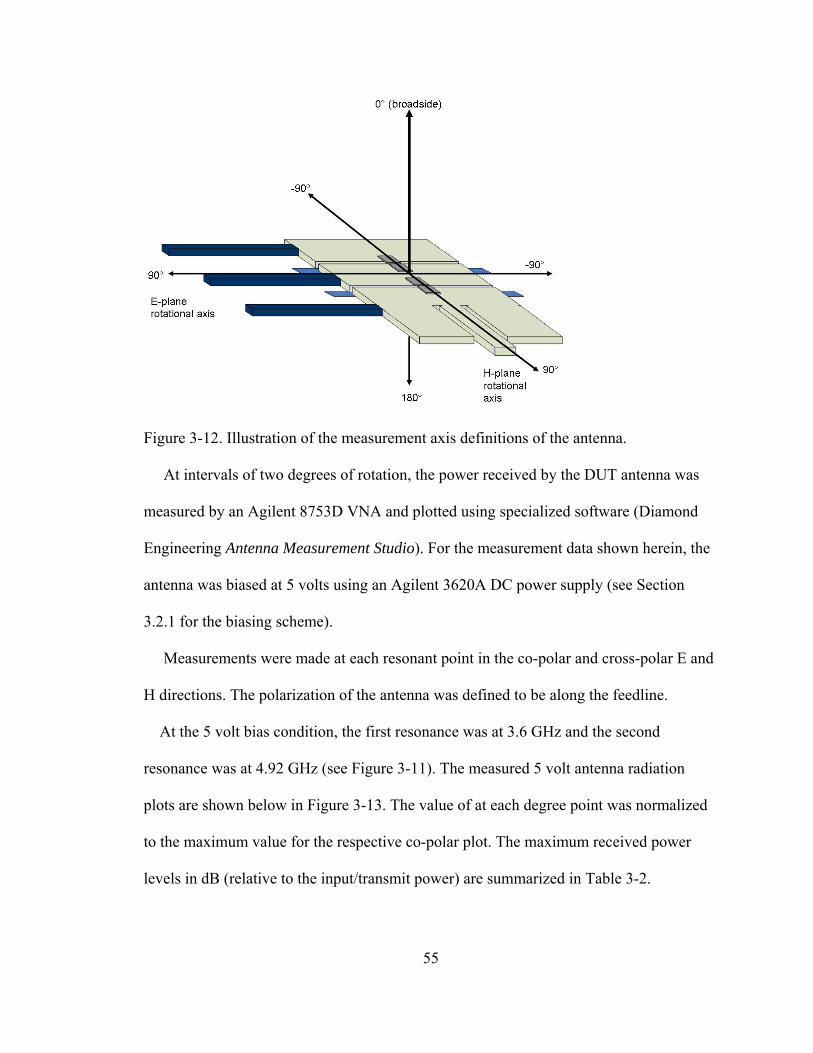
55
Figure 3-12. Illustration of the measurement axis definitions of the antenna.
At intervals of two degrees of rotation, the power received by the DUT antenna was
measured by an Agilent 8753D VNA and plotted using specialized software (Diamond
Engineering Antenna Measurement Studio). For the measurement data shown herein, the
antenna was biased at 5 volts using an Agilent 3620A DC power supply (see Section
3.2.1 for the biasing scheme).
Measurements were made at each resonant point in the co-polar and cross-polar E and
H directions. The polarization of the antenna was defined to be along the feedline.
At the 5 volt bias condition, the first resonance was at 3.6 GHz and the second
resonance was at 4.92 GHz (see Figure 3-11). The measured 5 volt antenna radiation
plots are shown below in Figure 3-13. The value of at each degree point was normalized
to the maximum value for the respective co-polar plot. The maximum received power
levels in dB (relative to the input/transmit power) are summarized in Table 3-2.

56
Figure 3-13. Measured 5 volt co-polarized and cross-polarized FPA radiation patterns.
Table 3-2. Maximum received power levels (relative to the transmit power) for each radiation pattern.
Resonance #1 Resonance #2 Pattern Level (dB) Pattern Level (dB)
Co-pol H -40.7 Co-pol H -42.59X-pol H -55.04 X-pol H -50.314Co-pol E -36.95 Co-pol E -37.99X-pol E -52.69 X-pol E -49.42
The performance of the antenna at 1st resonance was highly typical of patch antennas
operating in the fundamental TM10 mode. The performance at 2nd resonance was
consistent with documented patch antenna performance in the TM30 mode [23]. TM30
modes are typically characterized by a broadside circular pattern in the H-plane and a
three lobed broadside pattern in the E-plane [23]. Surface waves were expected to be

57
present at resonances above 4.7 GHz (see Chapter 2), and were likely partially
responsible for any minor deviation of the radiation patterns from the documented
standard patch antenna patterns.
Radiation pattern measurements were conducted for several bias points, and from
these measurements it was observed that the radiation patterns retained their basic shape
over the voltage tuning range. Therefore, it follows that the pattern shapes were mode
dependent not frequency dependent.
In general, while room for improvement remains, the measured radiation patterns were
considered to be explainable and useful in standard patch antenna applications.
3.3 Chapter Summary The preceding sections detail the simulation and measurement analysis of the FPA
Configuration #3. The simulated S-parameters and radiation patterns were useful in
predicting the measured performance of the FPA design.
From the S-parameter measurements, it was found that the two resonance points
overlapped at high and low bias, thereby expanding the operation bandwidth of the
antenna. The measured operational bandwidth was 63.4%.
From the simulated radiation patterns, it was found that the loss and the dielectric
properties (permittivity, thickness) of the FR4 substrate caused high inefficiency at the
second resonance point. Cross polarization levels were highest for the second resonance.
From the measured radiation patterns, the H-plane co-polarized levels at the second
resonance were improved, the patch antenna exhibited roughly TM30 performance at the
second resonance, and the radiation patterns at first resonance were similar to the

58
simulated values, except the cross-polarized levels were higher. Any deviation from
standard TM10 and TM30 radiation patterns were attributed to substrate effects (e.g.,
surface waves), feedline radiation, or general disruptions caused by the surface
discontinuities.
Possible areas of improvement are substrate choice and surface width design. In
addition, the use of more sections is a promising method of increasing the bandwidth
further.
The author considers that, based on the measured performance, such an antenna
design is a viable option in applications where tunable antennas are needed.

59
Chapter 4:
Varactor Development and Characterization
4.1 Introduction to BST Devices
Whenever conditions change in either a circuit itself or the application of a circuit, the
need arises to somehow dynamically adjust circuit parameters to accommodate the
changing demand. If the circuit cannot adapt itself to the new conditions, device
performance will suffer or fail completely; the benefits of dynamic circuitry are many,
which may include, smaller size, increased signal strength, low costs, and increased
energy savings [27], [28]. In addition to other technologies, Barium Strontium Titanate
(BST), or (Bax, Srx-1)TiO3, has been examined for this use for over 30 years [29] and in
increasing measure in recent years [28], [15]. BST is a family of ferroelectric/paraelectric
materials whose associated dielectric constant(s) are tunable with applied voltage.
This field-dependent permittivity makes BST an attractive choice for microwave
devices, since dielectric properties are often critical aspects of such electrically-large
systems. Dynamic phase shifters, filters, matching networks, and antennas are all among
the devices that have been re-designed to work successfully with BST.

60
Typically, the fundamental tunable components in these devices are varactors (or
tunable capacitors) [28], since capacitance is directly related to dielectric permittivity and
changing capacitance results in a changing capacitive phase shift, which is useful in many
of these devices.
For this work, the principle concern of the varactor design process was to develop
varactors that were suited for integration into the tunable antenna design described in
Chapters 3 and 4. This dictates that the varactors must be low loss and highly tunable.
They also need to possess low capacitance values in the range of 0.1 to 5 pF.
The following sections will give a high-level explanation of the theory, a description
of the development/implementation process, and a brief discussion of the measured
performance.
4.1.1 BST Material Properties Summary
BST is a high-permittivity dielectric material that has complex properties and
mechanisms. The purpose of this section (4.1.1) is to provide a high-level explanation of
the dielectric, tunability, and loss mechanisms of BST materials, since these properties
directly relate to the basic performance of varactors in antenna systems. The author
recommends Damjanovic et. al. [30] for a detailed explanation of the relevant material
principles.
Dielectric materials are characterized by a tendency to form electric dipoles in
response to the presence of an electric field [20]. The degree to which the structures in
the film are “willing” to form these dipoles (to be polarized, in other words), is
characterized by the electronic polarizability constant αe (α is general polarizability, αe is

61
the polarizability of a neutral atom), which is directly proportional to the magnitude of
the relative permittivity, or εr [12], [28]; the electronic polarizability and the relative
permittivity are related through equation (4-1), where N is the number of molecules per
unit volume and ε0 is the permittivity of free space.
0
1εα
ε er
N+= (4-1)
The relative permittivity is defined as the ratio of charge stored on two parallel
conductive plates with the dielectric between, over the charge stored without the
dielectric between. This value, multiplied by the permittivity of free space, ε0, comprises
the real part of the complex permittivity, or є’. The imaginary part, є’’, is directly
proportional to the loss tangent (tan δ) of the material. The real permittivity and the loss
tangent are often used to express the character of a microwave material [22]. The
molecular structure and mechanics of the material determines these two important
electrical parameters.
BST is a perovskite structure, and this family of materials is identified by the chemical
form ABO3 [15], [31], [28]. The simple cubic3 prototypical structure of this material is
shown in Figure 4-1.
3 Symmetric cubic structures form in the paraelectric phase only [28]

62
Figure 4-1. Perovskite family cubic molecular structure.
The ABO3 molecule is typically drawn with the B (Ti) molecule at the center position
and the A (Ba, Sr) molecules holding the corners [28], [15] as in Figure 4-1, but an
alternate configuration is presented in [31], where the A molecules hold the corners and
the unit cell is centered on the B molecule. Both configurations are equivalent.
When an external electric field is applied to the ABO3 structure, the molecular
structure deforms (the B molecule shifts position) and the polarization is increased, which
alters the relative permittivity [28] by lowering the polarizability constant α. The
application of this field and the resultant stretching causes the size of the lattice to
increase. To compensate, regions form within the lattice that are of various uniform
polarizations; these organizations of polarizations are referred to as domains and facilitate
the overall lowering of energy within the lattice [28], [12]. The sum total polarization,
composed of the individual dipoles in the lattice, is aligned with the applied field [12].

63
The dynamics of these domains in response to applied fields contribute to the dielectric
properties as much or nearly as much as does the individual molecular response [30].
When domain boundaries, known as walls, are free to move with a change in field
strength, the polarizability (and therefore the permittivity) is increased. Practically, this is
illustrated by the following scenario; as external large signal DC field strength increases,
the domain boundaries (known as walls) continue to adjust and form until saturation is
reached [28]. At this point, any incoming small-signal AC would only affect the direction
of atomic polarization, not the location of the domains, since they are now saturated. If
the large signal DC bias is removed, then any incoming AC signal would additionally
move the domain walls freely back and forth and/or freely create domains as the signal
voltage would alternate around 0 volts [28]. The decreasing domain wall mobility with
increasing field strength results in the bell-shaped permittivity/loss tangent vs. voltage
curve.
There are two primary loss mechanisms that result from this model. First, movement
of domain walls uses energy, and therefore AC signal loss is increased at 0 volts. Second,
regardless of the large signal voltage, small signal voltages cause alternating
molecular/atomic polar directions; switching directions also requires energy, and
therefore there is an inherent loss that is directly proportional to the polarizability in any
dielectric [28], [30]. An illustration of the permittivity vs. bias voltage curve is given in
Figure 4-2.

64
Figure 4-2. Typical ferroelectric permittivity vs. applied voltage curve.
Domain formation is not only seen upon the application of an external field, but the
effect may also be seen over temperature, particularly as it relates to the Curie
temperature.
The Curie temperature (Tc) is the temperature at which the film undergoes a transition
between the ferroelectric state (below Tc) and the paraelectric state (above Tc). For
microwave devices, the ambient temperature should be above the Curie point, so that the
film will operate in the paraelectric phase.
In the ferroelectric state, the molecules in the film are asymmetric and are therefore
polarized regardless of whether there is an external applied field or not (spontaneous
polarization) [15], [28], [30]; as noted above, this mechanism also causes the formation
of domains within the lattice (as do external electric fields) because of the spontaneous
polarization. In the paraelectric phase, the material has no natural polarization and
assumes the symmetric cubic structure shown in Figure 4-1. The primary consequence is
65
that a ferroelectric film will maintain its stretched shape after the external field has been
removed (known as hysterisis); a paraelectric film will return to its natural unit cell
structure. In summary, the primary difference between a ferroelectric film and a
paraelectric film is that for a ferroelectric film, domains and polarization exist without an
applied field, and, for an ideal paraelectric film, domains and polarizations exist only
with an applied field [28], [30].
The chemical notation for BST is given as (Bax, Srx-1)TiO3, where x is less than or
equal to 1. BaTiO3 (x=1) also works well as a tunable dielectric material, and for many
years was the primary material for this use, but the Curie temperature for this formulation
is roughly 110°C-130°C [32], [28], which can vary widely depending on whether the film
is bulk or thin[28]. Consequently, BaTiO3 is not suitable for use for most microwave
system applications where switching between permittivity states must be based on a
direct relationship between bias voltage and permittivity. For this reason, Strontium (Sr)
is included in BST; the addition of Sr lowers the Curie temperature significantly [28],
[33] so that the formulation is paraelectric at typical room/device operating temperatures.

66
4.1.2 BST Varactor Configurations Summary While there are many variations, there are two primary BST thin-film varactor
configurations: parallel plate and interdigital.
The parallel plate varactor [15], [31], [13], [34] is often used to characterize BST films
since the application of the standard capacitance equation is straightforward for this
configuration. Therefore, it is easy to extract the relative permittivity of the film once the
capacitance is known. These capacitors typically take on a variation similar to that shown
in Figure 4-3.
Figure 4-3. Typical parallel plate varactor concept drawing.
From Figure 4-3, it is evident that the field lines will originate from the signal line,
penetrate the BST and into the bottom electrode in the immediate area of the signal line.

67
The capacitive active region area is equal to the area of the signal line. The advantages of
this configuration are straightforward material properties extraction and low control
voltages. The disadvantages are complicated fabrication, dominant electrode loss [13],
and high capacitance values.
The second type of varactor configuration is the interdigital design [15], [17], [35].
Interdigital capacitors derive their name from the fact that the capacitor layout appears as
several interlocking fingers, as shown in Figure 4-4.
Figure 4-4. Typical interdigital varactor configuration concept drawing.
The field lines run between adjacent fingers, penetrating both the air on top and the
dielectric thin-film material (BST) beneath. Since the permittivity of the BST is
significantly higher than that of the air, the effective dielectric constant will be closer to
that of the BST, and the majority of the fields will concentrate in the thin-film dielectric.
The advantage of the interdigital configuration is that it is easier to construct, since it
requires only one metal layer. The disadvantage of the interdigital configurations is that
they suffer from reduced tunability and high operating voltages, since the distance
between the fingers is subject to photolithographic restrictions [35], [15].

68
4.2 Series Gap Capacitor Design 4.2.1 Design Overview The chosen device configuration (series gap capacitor) is similar to an interdigital
capacitor in that the dielectric lies beneath the conductive surface, and the capacitance is
between a gap in the metal surface. However, the device cannot be strictly referred to as
interdigital, since fingers are not necessarily included. Also, in the case of this design, the
gap can be as small as 200 nm, and is not subject to standard photolithographic
restrictions.
A non-tunable version of this design (without BST) was first presented by T. Ketterl
et. al. [19]. The design of [19] consisted of a co-planar waveguide structure whose signal
line contained a capacitive series gap positioned perpendicular to the direction of signal
travel. This slit, measuring between 200-800 nm wide and 45 um long, introduced a
series capacitance into the signal line. In the design of this work, the series gap was
positioned above a ~150-200 nm film of BST; the addition of the BST layer caused the
design to be capacitance-tunable. Focused ion beam milling was used to pattern the series
gap (refer to section 4.3.3 for an overview of FIB milling). The depth of this slit was
critical, since the depth could only reach to the bottom of the conductive metal and not
intrude into the BST layer; otherwise, tunability would have been compromised. The high
dielectric constant of the BST film (~300), ensured that a high percentage of the electric
field would concentrate within the film below the slit, not the air on top and inside the
gap. This configuration is illustrated in Figure 4-5 below.

69
Figure 4-5. FIB milled BST Series Gap Capacitor configuration.
Capacitance values for this device without BST underneath were reported by [19] to
be between 8 and 11 fF. This translates into approximately .18 fF/um to .24 fF/um. With
the introduction of the BST layer underneath the silt, this figure becomes dependent upon
the material composition of the BST. Estimations for the capacitance/unit length after the
addition of the BST were approximately .20 fF/um at high bias and .82 fF/um at 0 volt
bias.
4.2.2 Design Method
Four sample groups were fabricated for the purpose of experimenting with different
parameters of the series gap capacitor design. Specifically, BST pattern (confining the
BST region to under the cut only or to the whole wafer surface), cut depth, and substrate
choice were all examined.

70
The effects of the substrate and film composition are summarized in Sections 4.2.3
and 4.2.4, whereas cut depth is addressed in Sections 4.3.4 through 4.3.6. Table 4-1 gives
a summary of these sample groups.
Table 4-1. Summary of sample groups. Substrate Experimental Parameter BST Pattern
Sample Group #1 low resistivity Si general not patterned
Sample Group #2 high resistivity Si cut depth determination not patterned
Sample Group #3 high resistivity Si, MgO
cut depth, BST pattern, substrate patterned
Sample Group #4 high resistivity Si
cut depth, milling parameters, resist stripping methods patterned
All of the samples within a sample group were fabricated identically, except for group
#3 which contained devices parallel processed on both Si and MgO, in order to cross
compare substrate effects. Each sample within the sample group contained TRL
calibration structures and 25 individual devices. A device map is shown in Figure 4-6;
devices are named DVxy (x=row, y=column, DV is short for device).
Figure 4-6. Series gap capacitor sample device map.

71
4.2.3 Substrate Choice
Deposition of BST directly onto silicon substrates is typically not considered to be an
optimal solution, since there are crystallographic mismatches between the BST and the
silicon, a low permittivity oxide film may form between the Si/BST interface during BST
sputtering, and high-resistivity silicon may loose its resistivity when subjected to high
temperature [18]. Lattice mismatch may cause mechanical stress and reduced tunability
due to the crystallographic structure of the resulting BST film [18].
However, based on measurement results from Samples #2-4, BST on Si does give
good dielectric tunability and loss performance up to 65 GHz when high resistivity Si
(3000-5000 ohm-cm) is used. Measurement of Sample #1 served to show that device
performance is unacceptable on low-resistivity Si. Other substrate choices that are
considered to be optimal are LaAlO3, MgO, and Al2O3 in both the polycrystalline
(Alumina) and the single crystal states (Sapphire) [15], [36], [17]. It is expected that
performance will increase significantly for films deposited on these substrates over films
deposited on HR Si. Although a sample was fabricated on MgO (Sample #3), the FIB
milling could not be carried out due to imaging problems that were mostly likely related
to the resistivity of the MgO material. This problem is expected to be solved in the future
by improving the grounding of the sample surface.
4.2.4 Film Composition and Thickness The two primary parameters that control the microwave response of BST films are
film composition and thickness.

72
Thicker films generally have better tunability and higher dielectric constants [31],
[15]. In addition, thicker films require higher tuning voltages. For this device design,
capacitance values are much smaller than is needed for the antenna application, and
tunability is a highly valued quantity, so thicker films are the preferred choice.
Film composition determines film response and controls tunability, loss, and the Curie
temperature.
The Sr content in the film has a direct effect on both the dielectric constant and the
Curie temperature. Both the dielectric constant and the Curie temperature are inversely
proportionally to the Sr content [15]. The addition of Sr to BaTiO3 lowers the Curie
temperature; it has been reported [28], [33] that Tc drops 3.4°C for every percent increase
in the Sr content of the BST film. For a BST composition of (Ba.5, Sr.5)TiO3, the Curie
temperature is approximately -50 °C, which is adequate for tunable devices. Although the
Ba/Sr=.5/.5 ratio was used for the devices in this work, further work may be done to
optimize the film for this specific application. Studies [28] have shown that tunability and
loss tangent is maximized when the device operating temperature is both above and near
the Curie temperature.
The Ti content, as expressed by the (Ba+Sr)/Ti ratio affects dielectric loss and
tunability. Higher ratios (lower Ti content) provide better tunability, while lower ratios
(higher Ti content) give better loss characteristics/quality factors [15], [37]. The Ti
content is controlled by oxygen concentration during sputter-deposition [15].

73
4.2.5 Design Summary The chosen varactor design is based on the work presented in [19], and is expected to
provide good tuning ratios, good loss performance, and straightforward integration into
tunable antenna systems. The design parameters and their significance are summarized in
Table 4-2. These parameters are largely determined by fabrication process methodology,
and this process is detailed in Section 3.3.
Table 4-2. Device design summary. Parameter Related Performance
Cut Depth and Width capacitance, tunability Film Thickness capacitance, εr value range, bias voltage range Film Stoichiometry dielectric loss, tunability Substrate Properties quality factor, structural integrity, frequency of operation Electrode Conductivity quality factor
4.3 Device Fabrication 4.3.1 BST Deposition Approximately 100-200 nm of BST was sputter-deposited onto high resistivity (3000-
5000 ohm-cm) Si. The composition of the BST target was (Ba.5, Sr.5)TiO3. The
parameters for BST deposition were adopted from Manavalan [15]; here, extensive
research was done in order to optimize BST sputter-deposition for numerous substrates
and deposition methods. The primary parameters of consideration in BST sputtering
were the argon/oxygen gas ratio and the process temperature. Both of these parameters
have an effect on film crystallinity, while gas pressure additionally influences
stoichiometry [15] and therefore the critical (Ba+Sr)/Ti ratio. Increasing the process
temperature has been shown [15] to increase the XRD peak intensities for many crystal
orientations.

74
The sputter deposition process parameters used for all devices in this work are
summarized in Table 4-3 below.
Table 4-3. BST sputter-deposition parameters. Parameter Setting
RF Power (W) 150Ar/O2 Ratio (%) 90/10Total Pressure (mTorr) 25 Thickness (nm) 100-200 Temperature (°C) 650
The XRD spectrum for Sample #2 is given in Figure 4-7. The BST <110> and <200>
orientation peaks are visible. The spectrum was obtained from a film deposited on a
separate wafer alongside the device wafer of Sample #2.
Figure 4-7. XRD spectrum plots from sample #2.

75
4.3.2 Photolithography and Etching The general photolithographic process for the construction of the series gap capacitor
device described in Section 4.2.1 is graphically summarized in Figure 4-8. The
exhaustive process flow is provided in Appendix B, and is summarized in the paragraphs
below.
Figure 4-8. Photolithographic process illustration for the series gap capacitor.
Between step 1 and step 2, the protective oxide layer was removed through a 10:1
BOE etch. In step 3, the BST was deposited by sputter deposition, as described in Section
4.3.1. The BST was then patterned by positive resist lithography and a second 10:1 BOE
etch in step 4, followed by negative resist patterning and subsequent thermal deposition

76
of the top metal, Au, in step 5. In steps 6 and 7, PMMA (polymethal methalcrylate) was
spun on to a thickness of ~2000 angstroms, and a thin layer of Cr was deposited on top.
The PMMA served to support the Cr and separate it from the Au for later removal. The
Cr was necessary for FIB milling to provide a conductive top surface to assist in beam
focusing (see Section 4.3.3) [19]. In step 9, following the FIB milling in step 8, the
PMMA and the Cr was removed by an acryl strip. This process was developed largely by
trial and error and by synthesizing the work specifically presented in [15] and [19]. A
finished device is shown in Figure 4-9.
Figure 4-9. Finished series gap capacitor signal line showing misaligned BST region.
There are three things which should be noted carefully when fabricating these devices.
First, misalignment of the BST region is not as benign as it may seem. From Figure 4-9 it
can be seen that the BST region is not completely covering the bottom side of the signal
line; a small amount of the Au signal line is in direct contact with the Si. All devices
fabricated in this manner broke down (that is, DC current flowed freely across the gap)
upon application of ~8 Volts DC. The hypothesis was that the Si caused the premature
breakdown for the following reason: whenever the BST region is misaligned, the
breakdown voltage of the device becomes subject to the breakdown voltage of the Si if

77
the breakdown voltage is lower than that of the BST. The breakdown voltage of Si
depends on doping concentration, and is lower than that of BST in some cases [38], [39].
Due to low mask dimension tolerances, avoiding this effect is practically unavoidable for
the entire 5 by 5 device field; nevertheless, devices with this level of mis-alignment
should not be used.
Second, trace amounts of photo-resist left after the positive resist step can have a
terminally adverse effect on the devices during the measurement phase. It is currently
held by the author that trace amounts of residual positive resist left after the BST etch
step can cause bubbling of the Au layers upon application of voltages above ~5 Volts.
This effect was seen for Sample #3 and destroyed the device by eroding the walls of the
FIB milled gap. This effect was eliminated in subsequent samples by some or all of the
following steps: thinner resist was used (Shipley 1813 instead of 1827), resist was
removed by MicroChem® 1165 photoresist strip, and/or any further residual resist was
removed through an oxygen plasma etch for 2 minutes. The plasma etch should be
avoided if possible, since it has been reported that RIE etches have damaged BST films
and caused reductions in tunability [31].
Third, it was observed that the ion beam interacts with the PMMA and makes it
resistant to stripping. It was experimentally determined that using MicroChem® Acryl
strip was the most effective and non-destructive method employed in this work to remove
the PMMA after milling. However, there is currently no known effect of residual PMMA
that is detrimental to device performance.

78
4.3.3 Focused Ion Beam Milling Introduction First developed in the 1970’s [40], Focused Ion Beam (FIB) Milling is an emerging
means for manipulation of material structures at the nano-scale. In an FIB system,
material is sputtered from a target (the sample) by a beam of highly focused impinging
Gallium ions; these ion beams can be as small as 5 nm meters in width (50 angstroms),
and because of the small beam area, high-precision micro-machining is possible. The
beam can be directed to cut in highly complex patterns by data files and even picture
files. Researchers are continuously finding new ways to apply this high-potential
technology; in fact, one researcher recently used focused ion beam milling to construct a
nano-wire jungle gym on top of a human hair [41]. Common applications include
destructive device testing, modification, mask repair [42], sample preparation [43], and
MEMS fabrication.
The mechanics of a typical ion beam system are similar to that of a scanning electron
microscope, or SEM [43]. In an SEM, an electron source scans an electron beam across
the surface of the sample and a secondary electron detector receives the electrons coming
off of the sample; the microscope generates an image from the incoming electrons. In an
ion beam, a liquid metal ion source (LMIS) supplies a stream of focused Ga+ ions by
way of a complex lens-focusing system and finally through a thin tungsten needle [43].
When the accelerated Ga+ ions strike the surface of the sample, secondary electrons,
secondary ions, and neutral molecules are removed from the surface [42]. It should be
noted that the term secondary refers to the particles that are removed from the material as
a result of the impinging beam. This process is illustrated in Figure 4-10.

79
Figure 4-10. Illustration of the Focused Ion Beam milling system.
Instead of moving in a continuous scan, the beam makes a series of successive “hits”,
analogous to making a line with a hole punch. These hits are sometimes referred to as
pixels. The beam raster scans along the cut pattern until the desired depth is achieved.
The raster scan process is largely controlled by the user, primarily through the following
parameters: dwell time, z-size, % overlap/pitch, and beam current. Dwell time is the
length of time that the beam spends per pixel, percent overlap/pitch is the degree to which
each hit overlaps the preceding hit (also expressed by the term pitch—see Figure 4-11),
beam current is the strength of the ion beam (higher beam current results in faster milling
and larger hit diameter [42]), and z-size is the desired cut depth.

80
The width of each pixel is also determined by focusing; this concept is intuitive, since
if the beam is focused on a point 5 inches below the sample, then it follows that the beam
incident on the sample surface will be wider than it would at the focus point.
The raster scan pattern for a single pixel wide slit is illustrated in Figure 4-11.
Figure 4-11. Illustration of beam raster scanning and the relationship between pitch and percent overlap. As the particles are removed from the surface of the sample, a current is generated in
the sample that flows to ground. The magnitude of this current is directly proportional to
the beam current and loosely related to the sputter yield of the material being removed, so
if the current flowing to ground (or absorbed current) is measured, then a rough
evaluation of sputtering yield can be obtained [42]. This technique is discussed in detail
in Section 4.3.5, and is referred to as End Point Detection (EPD), or End Point Monitor
(EPM).
Focused Ion Beams can also be used to deposit certain metals, such as Pt [43]. The
simple explanation for this process is the following: the metal to be deposited is carried
by various gases from the gas injector (see Figure 4-10) to the surface of the sample and
the Ga+ ion beam forces the metal to the surface in the desired pattern [42].

81
It is also necessary that the sample is coated with a thin layer (~50 angstroms) of
conductive material to neutralize the sample surface. Otherwise, a strong charge will
develop on the surface and will repel the ion beam, resulting in poor beam focusing [19].
Since for this application it was critical that the beam not enter the BST layer, a
milling procedure was developed to stop the beam at the interface between the gold and
the BST layers.
4.3.4 Focused Ion Beam Milling Methodology
General FIB milling parameter settings are summarized in Table 4-4. The majority of
these parameters were determined experimentally and the experimental process is
discussed in Section 4.3.5.
Table 4-4. Milling parameter summary. Parameter Setting Effect Comments
Z-size varied milling depth value dependent upon desired cut depth Dwell Time 1 usec unknown value used for all devices Overlap 0%, 50% trench roughness 50% was used to reduce residue inside trench
Length ~60 um length of trench trench traversed entire width of signal line with excess for this length
Beam Current .3, 3 nA milling time, spot
size
beam current must be increased to at least 3 nA for 50% overlap—minimum system requirements may also vary depending on various milling conditions
The primary difficulty with the FIB/BST capacitor fabrication was the task of cutting
a trench to a depth that completely cut through the metal and did not cut into the BST.
For single layer compositions, the cut depth (or z-size) for FIB milling is governed
adequately by material-characterization data. When the user enters the desired cut depth
(z-size), the software uses the characterization data to determine the optimal cutting time
to achieve this depth, based on the user-specified milling parameters (e.g., % overlap,

82
dwell time, etc.). For multilayer devices, this basic approach is largely invalid, since
each different material has different properties, specifically density/sputter yield and
stopping power [43].
The following two methods were explored to determine the proper cut depth: method
(a), cross-sectional metrology and method (b), end point current monitor data. Although
their use was not explored in this work, software such as SRIM and TRIM have been
developed to model the ion-solid interactions for complex materials [43], and may also be
useful for this application. The success of each cut was judged through a combination of
passing DC current across the gap (to determine whether the gold had been severed
completely) and making RF measurements to determine the tunability (and therefore the
integrity) of the BST film. In the event that a cut comes just short of penetrating the Au
layer, experiments have shown the remaining metal can be removed by passing 30-50
mA of current through the semi-open slit.
Method (a), cross sectional metrology, was accomplished by using the FIB to create
several slits of different cut depths, deposit a thin strip of platinum perpendicular to the
slits, and use the FIB to create a deep hole that traversed each slit and dissected the
platinum strip (see Figures 4-12 and 4-13). The purpose of the deep hole was to open a
cross-sectional viewing area; the floor of the hole was deepest at the cross-sectional wall
and sloped up toward the viewing location. The sloped floor was created to minimize
milling time. The deposited Pt filled in the slits so that the depth could be more
accurately judged from the cross-section view.

83
Figure 4-12. Top down schematic view of the cross-sectional depth experiment.
Figure 4-13. Top-down SEM image of the cross-sectional destructive test setup. This picture was taken from Sample #1, where the BST covered the entire surface of the wafer.
After the structure of Figure 4-13 was milled, the sample was rotated in such a way
that the wall of the deep hole that contained the cross-sections of the cuts could be
viewed.

84
When the microscope was oriented and zoomed correctly, the cross sections of each
cut could be viewed with great detail as well as the individual layers of the multi-layer
structure (see Figure 4-14).
Figure 4-14. Cross-sectional ion-beam image of a FIB milled slit in the signal line.
Note the pencil-like shape of the FIB cut profile; the point of the tip is the focus point
of the beam. The shape/slope of this cut profile varies depending on beam focusing and
layer thickness, and can cause the variation in cut width between the top of the cut and
the bottom of the cut to be as much as 300%4. In Figure 4-14, it appears as though the cut
penetrated the BST layer. As noted previously, the appropriate cut depth should reach the
top of or slightly above the BST layer. Under method (a), once the ideal depth has been
determined, this value would be entered into the z-size parameter of the milling software
and used for all devices on the sample.
4 Value was estimated by extrapolation and is subject to variation and error. Minimum beam spot size is generally ~5 nm.

85
This method is ineffective by itself to provide a means of repeatable cut depth, since
the thickness of each individual layer (particularly the PMMA) varies between place to
place on the wafer and between different samples. However, when used in conjunction
with the use of end-point current detection data (EPD), it is an effective technique.
Method (b) makes use of end-point current detection data to determine in-situ the cut
depth of the beam scan. This method was proven in experiments to be a repeatable
method of determining cut depth both in this work and by Latif et. al. [42]. End-point
detection monitors changes in sample current as material is removed from the sample
surface. When particles are removed from the sample, they either are re-deposited on the
sample surface or they disappear from the sample altogether; in either case, neutralization
current must flow from the sample to ground. The general equation for determining
sample current based on particle removal is given by (4-2) below [44], where Isample is the
total current measured by a current meter between the sample and ground, Ibeam is the ion
beam current from the source, ISe- is the current due to the departure of secondary
electrons (or other negative charges), and ISi+ is the current due to the departure of
secondary positively charged ions.
+− −+= SiSebeamsample IIII (4-2)
The sample current due to re-deposited particles is illustrated by Figure 4-15.

86
Figure 4-15. EPD process illustration. Refer to (4-2) for mathematical characterization.
From Figure 4-15, the sample current flow is generated by charges appearing through
re-deposition on the surface of the sample. The net surface charge is a result of secondary
ions, secondary electrons, and Ga+ ions from the source. Based on Figure 4-15 and the
model derived from (4-2), the sample current should be directly proportional to the
sputtering yield of the layer being milled at any instant in time. This is a true but
simplistic view, since the sample current at one milling layer is also expected to be
dependent upon certain ion-solid interactions, such as backscattering and implantation
[43] that may have occurred during the milling of preceding layers. Specifically, in the
case of backscattering, when an incident ion strikes the surface of the sample, the energy

87
can either be returned to the incident ion (in the case of non-elastic interaction), causing
backscattering and re-deposition or be transferred to the sample molecules (in the case of
elastic interaction), causing secondary ion and electron generation. Upon arrival at the
sample surface, the ion may also implant into the material, where its excursion into the
material depends upon the stopping power of the material [43]. To summarize, the
relationship between sample current and material properties is complex and multifaceted.
The author recommends [43] for a full treatment of this topic.
Figure 4-16 shows a sample EPD graph for a Cr-PMMA-Au-BST-Si structure. The
graph contains multiple phases which are associated with different materials in the
multilayer structure. The depth of this cut extended well into the Si region.
Figure 4-16. Sample EPD graph showing milling time vs. absorbed current. Numbers indicate different regions in the multilayer structure.
4.3.5 Depth Optimization Experiments Using End Point Detection
Upon inspection of the graph in Figure 4-16, the initial hypothesis considered region
1-3 to be the Cr layer, region 4 to be the PMMA region, region 5 to be the Au layer, and

88
region 6 to be the BST/Si areas. Region 7 is invalid since, this drop in current was created
during beam shutoff. This hypothesis assumed a direct correlation between increased
sample current and material conductivity.
The first test on this hypothesis was to fabricate a device (Sample #2, device 22)
where the beam shutoff time reached the maximum of phase 5. After milling, 15 volts
DC was applied across the slit and some current flowed initially, but quickly went to zero
within seconds. This indicated that some metal was left, but was burned off with current;
this would seem to corroborate the initial hypothesis.
The second test on this hypothesis was to fabricate a set of samples with patterned
BST regions (the BST region was confined to the area in the vicinity of the capacitive
slit) and compare the EPD data with and without the BST region. Several lines were cut
across the portion of the signal line lying directly over top the BST region and several
lines were cut across the portion of the signal line lying directly over the Si substrate.
Both the cross-sectional images and the EPD data were obtained for both types of lines.
Figure 4-17 shows the top down view of these lines after milling. The edge of the BST
region can be clearly seen; it appears as a raised section of metal. The EPD graphs for
these lines are shown in Figure 4-18.

89
Figure 4-17. Top down SEM image of test lines and cross sectional viewing region. The edge of the BST region is indicated with an arrow; lines 5-7 are located over the BST region and line 4 is located outside the region.
Figure 4-18. EPD data graphs for lines 4-7.

90
The relationship between the graph of 4 and the graph of 5 is of critical importance.
From Figure 4-18, it is apparent that the stopping time of line 4 lay outside of the BST
region whereas the stopping time of line 5 was inside the region. Both lines were milled
with a z-size setting of 3 um. Notice that region/phase 5 was missing from the graph of
line 4. The conclusion from this finding was that phase 5 must have resulted from the
presence of a BST layer; this conclusion contradicts the initial hypothesis. The new
hypothesis was that phase 1 was the Cr, phase 2 was the PMMA, phase 3 was the Au,
phase 5 was related to the BST layer, and phase 6 was associated with the Si layer.
However, there is insufficient evidence to suggest that phase 5 directly indicates that the
milling depth is at the BST during phase 5. Latif [42] suggests that the interpretation of
the EPD data from insulators is not always straightforward, as it generally is with
conductors. Possible explanations for the increase of sputtering yield in the vicinity of the
BST layer could be (a) interaction between the Si and BST during the sputtering of the
BST thin-film [42], (b) stray impurities lodged in the interface between the BST and the
gold layers [42], and (c) accumulated Ga+ ions inside the BST film from previous elastic
ion interactions in previously milled layers. The drop in sample current at phase 4
appears to representative of an interface effect, most likely between Au and BST.
From Figure 4-18, the stopping times of lines 6 and 7 were located inside the BST
region. Line 6 clearly did not reach the bottom of the gold layer, and perhaps not even the
PMMA layer. The EPD graph of line 6 shows that the milling stopped at the peak of
phase 3. It is assumed that phase 3 is the Au layer, since phase 1 is most likely associated
with the Cr layer.

91
Based on this comparison, the new hypothesis was that phase 3 was Au and phase 5
was BST. Under this method, it was assumed that the proper milling time for optimal cut
depth would be in phase 4, and therefore line 7 was created; the EPD data for line 7
indicated that milling was terminated at the end of phase 4 (see Figure 4-18). The cross
sectional image for line 7 is shown below in Figure 4-19. The location of the BST layer
can clearly be seen from Figure 4-19 right, since the edge of the pattern is apparent on
both the surface and the cross section.
Figure 4-19. Cross sectional ion-beam images of lines 7 and 6 (left), and lines 5 and 4 (right). From Figure 4-19, although it is difficult to discern, the cut depth of line 7 did not
penetrate the BST layer. The cut of line 5 either fully or partially penetrated the BST
layer. DC measurement of a line with similar EPD data to that of line 7 indicated
irreparable conductivity (the metal could not be removed through amperage) across the
gap.
An alternate theory that also agrees with the data is that the insulating materials (with
the exception of Si) resulted in higher net sample current than did the conductors. Under

92
this theory, the initial high sample current in phase 1 would have to be due to an ambient
grown oxide on the surface of the Cr. This would make phase 2 the Cr, phase 3 the
PMMA, phase 4 the Au, and phase 5 the BST.
Since for both theories, phase 4 was supposed to correspond to the optimal stop time
for milling, a theory was developed for why the gap remained conductive. Upon close
examination of lines 4, 5, and 7 from Figure 4-19, the bottom surface of the trench
appeared rough, with the topology varying significantly over the length of the cut. The
hypothesis was that this effect resulted from an interaction between beam focus depth and
the 0% overlap setting. It was supposed that a 50 percent overlap would yield an overall
cleaner cut, and thereby create a smoother trench floor yielding in turn better depth
precision. Figure 4-20 gives a comparison between two lines with similar EPD (milling
terminated in phase 4), but with different overlap settings. It should be noted that the
milling software required that a higher beam current be used for the 50% setting (3 nA).

93
Figure 4-20. SEM image comparing two trenches with a 0% overlap setting (left) and a 50% overlap setting (right). It is evident from Figure 4-20 that the 50% overlap setting yielded both a cleaner and
narrower cut. The general effect on the initial conductivity across the gap was that the
cut depth (via milling time) could be moved slightly closer to phase 4 from phase 5
without causing irreparable shorting.
4.3.6 Discussion and Summary of Milling Procedures
The following conclusions may be made from the results of Sections 4.3.4 and 4.3.5:
First, ion beam excursion must be limited to the top of the BST layer. Single material
characterization files are not applicable for depth control in multilayer structures.
Second, cross sectional metrology is ineffective by itself as a repeatable method of
depth control. When used in combination with end-point detection data (EPD) it is a
powerful means to examine the quality of FIB trenches.

94
Third, EPD can be effectively used to determine in-situ the progress of the beam into
the multilayer structure. EPD current may be linked loosely with material sputter yield,
but ion scattering/re-deposition and implantation effects must all be considered. Different
phases in the EPD data were identified and roughly associated with different material
layers in multilayer structure. Through DC and RF measurement, the optimal cut depth
(as expressed by EPD data, not z-size) was determined. The % overlap setting mildly
affected the optimal cut depth.
Fourth, it is not known whether phase 5 was directly associated with the bulk of the
BST layer.
Fifth, the optimal cut depth was achieved when milling time reached the top of phase
5 for 0% overlap, and approximately halfway between phase 4 and 5 for 50% overlap.
Following this guideline, working capacitors can be constructed on a generally consistent
basis. The milling time regions and their results with respect to EPD phases are
summarized in Figure 4-21.

95
Figure 4-21. EPD approximate region analysis summary. No experimental data was collected for phases 1 and 2. 4.4 Device Characterization 4.4.1 Measurement Setup and Device Properties
S-parameter measurements of the series gap capacitors were made using an Anritsu
37397C Lightning network analyzer, an Agilent E3620A DC bias supply, NIST MultiCal
software, and two GGB 150 micron pitch ground-signal-ground 67A-GSG-150-P probes.
A 1.5k-ohm resistor was placed in the bias line to prevent high short-circuit current levels
from damaging the probes or the bias tees.
Sample #4, device 12 was chosen to be the object of the characterization study, since
it exhibited the best tunability and structural integrity (i.e., low DC conductance across
the gap/high breakdown voltage). A SEM image of this device is shown in Figure 4-22.

96
Figure 4-22. SEM image of sample #4, device 12.
The series gap in this device was cut using the 50% beam overlap setting and was cut
at the far/top edge of the 50% optimal region extension area. DC measurements indicated
that there was no trace of gold left after the milling, so it was expected that some of, but a
minimal amount of the BST was milled. The EPD graph for this device is shown below
in Figure 4-23.
Figure 4-23. Device 12 end-point detection graph.

97
4.4.2 Calibration
Separate S-parameter measurements were made using both TRL (thru-reflect-line) and
probe-tip SOLT calibrations. The motivation for using the additional probe-tip calibration
was to prevent an observed phase/impedance shift from occurring outside of the reference
planes due to the application of bias across the CPW line. The change in waveguide
propagation due to the application of bias was experimentally related to Silicon-specific
effects. While it was possible to perform separate calibrations at each bias point, this
approach necessarily forced one side of the CPW line to a bias condition not included in
the calibration (since during calibration the waveguide had to be uniformly biased at all
ports). The calibrated frequency range was 40 MHz to 65 GHz for the TRL calibration
and 40MHz to 20 GHz for the probe-tip calibration.
The TRL calibration was designed with five CPW delay lines, a CPW 0-length THRU
line, and a CPW 0-length open line. The delay line lengths along with the CPW
dimensions are given in Table 4-5.
Table 4-5. TRL calibration delay line lengths and CPW dimensions. Line # Length CPW Gap W Ground Plane W Signal Line W
Delay 1 0.7 mm 27 um 200 um 45 umDelay 2 0.95 mm 27 um 200 um 45 umDelay 3 1.6 mm 27 um 200 um 45 umDelay 4 2.2 mm 27 um 200 um 45 umDelay 5 3.8 mm 27 um 200 um 45 um
The TRL calibration using all four delay lines was only successful when the standards
were situated above a BST/Si structure. Calibration with all delay lines was not
successful when the lines were placed directly on the HR Si substrate (in the case of
Samples #3 and #4). The cause of this problem is not known. Instead calibration was

98
performed using delay line #4, which gave adequate phase coverage across the frequency
range of interest.
The probe-tip calibration was conducted using a GGB CS-5 SOLT calibration
substrate.
4.4.3 Measurement and Characterization
The following two sets of measurement data are presented below: S-parameter data
obtained to 65 GHz using a TRL calibration and S-parameter data obtained to 20 GHz
using a probe-tip calibration. Approximate series capacitance data was extracted from the
TRL calibrated S-parameter data using an equivalent pi network.
Figure 4-24 below shows the S21 data obtained using a TRL calibration and at bias
voltages 0, 1, 3, 5, 10, 15 and 25 volts. Figure 4-25 shows the S11 data for this device
obtained with a TRL calibration and taken over the same bias voltage range.

99
Figure 4-24. S21 TRL data for sample #4, device 12. The top curve is for 0 volt bias and the bottom curve is for 25 volt bias.
Figure 4-25. S11 TRL measurement data for sample #4, device 12. The top curve is for 25 volt bias and the bottom curve is for 0 volt bias. The low frequency positive S11 data for bias voltages 5, 10, and 25 volts were
attributed to transmission line effects outside the reference planes due to the application
of bias between the signal and the ground lines of the co-planar waveguide. For this
reason, additional measurement data was obtained using a probe-tip SOLT calibration; in

100
this way, any bias-related performance changes would take place inside the reference
planes of the calibration.
Figure 4-26 below shows S21 and S11 over bias voltages 0, 1, 3, 5, 10, and 20 volts;
these measurements were obtained using a probe-tip SOLT calibration to 20 GHz.
Figure 4-26. S21 (left) and S11 (right) SOLT measurement data for sample #4, device 12. The top curve in the S21 data is 0 volt bias and the top curve in the S11 data is 20 volt bias. The phase data obtained for both calibration methods across the full bias range is
shown in Figure 4-27. The phase difference between the calibration methods resulting
from the narrower reference planes in the TRL calibration is apparent.
Figure 4-27. Measured S11 phase data from sample #4, device 12. Both SOLT calibrated data and TRL calibrated data are shown.

101
Approximate series capacitance values were extracted5 from the TRL calibrated S-
parameter data using the equivalent pi network [22] shown in Figure 4-28.
Figure 4-28. Equivalent 2-port admittance pi network.
The value of the series capacitance Cs was extracted from this circuit using ABCD
parameters (calculated from S-parameter data) and equations (4-3) and (4-4) [22], where
Y3 is the complex series admittance of a two port network.
BY 13 = (4-3)
ω)3Im(YCs = (4-4)
The result of (4-4) was plotted over a frequency range between 40 MHz and 65 GHz at
bias voltages 0 and 25 volts. These results are shown in Figure 4-29. The numerical
results of the extraction are tabulated in Table 4-6.
5 Evelyn Benabe, University of South Florida

102
Figure 4-29. Extracted series capacitance (Cs) vs. frequency at bias voltages 0 and 25 volts. Table 4-6. Extracted Cs values over frequency.
1 GHz 3 GHz 5 GHz 10 GHz 20 GHz 60 GHz 0 Volts 84.7 fF 49.8 fF 35.2 fF 22.9 fF 16.7 fF 13.2 fF 25 Volts 6.4 fF 8.3 fF 9.05 fF 9.8 fF 10.3 fF 10.8 fF Ratio 13.2 6 3.9 2.3 1.6 1.2
4.4.4 Summary
S-parameter data was taken at frequencies between 40 MHz and 65 GHz. There were
no resonant points observed across this frequency range. TRL calibration caused slightly
inaccurate measurement results since the application of bias along the line affected signal
propagation and this effect occurred outside of the measurement reference planes. A

103
probe-tip calibration was conducted to move the effect inside the reference planes.
Approximate series capacitance values ranged from 6.4 fF to 84.7 fF and were heavily
frequency dependent.
4.5 Chapter Summary
BST devices are useful for microwave systems, such as the antenna developed in this
work, that need to dynamically adjust operating parameters to conform to changing
environments. The chapter above outlines the development of a device that has the
potential to deliver high tunability, low loss, and planar integration.
The permittivity characteristics of BST are governed by the changing molecular/lattice
structure of the BST upon applied bias. This feature of the BST leads to bias-dependent
permittivity and loss characteristics.
Focused ion beam milling was used to create series gaps in the signal line of a co-
planar waveguide. Significant experimental work was conducted to optimize the cut
depth so that the integrity of the BST thin-film layer would not be compromised. End-
point current detection proved to be a repeatable method to control the excursion of the
beam into the multilayer structure.
Measurements were conducted on a device that was fabricated using the end-point
current method; approximate capacitance values (averaged over frequency) for this
device ranged from 9 fF to 37 fF (~4:1 tunability). In general, devices with like EPD
profiles had similar performance characteristics.
This research lays the groundwork for future tunable devices and a deeper
understanding of the performance of BST films as they relate to the series gap capacitor

104
configuration. The constructed configuration is appropriate for integration into the
tunable antenna presented in this work, because the capacitance size can be tailored to the
application by adjusting the series gap length, the design lends itself to planar integration
and the devices are expected (analysis is not mature) to exhibit loss and tuning
characteristics that are appropriate for antenna applications.

105
Chapter 5:
Summary and Conclusions
The overarching purpose of this project was to realize a patch antenna whose
operational bandwidth and ease of fabrication exceeded that of other current design
solutions. The antenna developed in the pages of this work fulfilled this purpose by
delivering a wide operational bandwidth while maintaining straightforward integration
and design.
While not fundamental to the success of the design, the integration of the antenna with
Barium Strontium Titanate varactors was considered to be a useful extension of the
research. The varactors whose design methodology and performance are described in the
pages of this work are expected to integrate cleanly with the antenna without
complicating fabrication or compromising performance significantly. The possibility of
integrating the BST with the antenna would simplify monolithic integration considerably,
since the design of the varactor is planar, requiring only two photolithographic mask
layers.
The following section provides a high-level summary of the findings reported in this
work.

106
5.1 Summary of Findings
5.1.1 Tunable Antenna Using Semiconductor Varactors
The following paragraphs are a summary of the main aspects of the antenna design
process and results. Figure 5-1 shows the finished Fragmented Patch Antenna (FPA) with
installed semiconductor varactors.
Figure 5-1. Completed Fragmented Patch Antenna using semiconductor varactors.
The antenna was developed through an optimization procedure. This procedure
directly analyzed the parameters of the antenna including, the number of sections
composing the radiating surface, the capacitance range of the varactors, the size of the
sections, the width of the antenna, and other design features.
It was discovered through this procedure that the antenna could be designed to have
multiple overlapping resonant regions. This aspect could be exploited to produce an
antenna with a tuning bandwidth that would be limited only by the input matching
characteristics.

107
The outcome of the optimization process was an antenna with three equal section
lengths and widths, two equal capacitors (one for each gap), and an inset feed. Specific
areas for improvement are antenna substrate, antenna width, the number of radiating
sections, and input matching.
The S-parameter and radiation pattern simulations indicated that the antenna was
highly tunable, but that the radiation patterns were significantly altered by the modified
patch antenna configuration. The S-parameter measurements generally corroborated the
simulated results.
The simulated radiation patterns were largely distorted from typical patch antenna
patterns due to the effects of surface waves and substrate loss. The measured radiation
patterns indicated that the fundamental resonant mode of the antenna operated similarly
to that of a standard patch antenna. The second resonance mode was loosely linked to a
higher order patch antenna mode. The radiation pattern measurements indicated that the
radiation characteristics had retained enough pattern integrity to make the antenna a
viable solution.
Because the antenna exhibited excellent tunability with usable radiation patterns, it is
a recommended design configuration for situations where a wide bandwidth antenna is
needed.
108
5.1.2 Barium Strontium Titanate Nano-Scale Varactors
• Focused Ion Beam milling is a micro-machining tool that can be effectively used
to mill nano-scale structures on the surface of a wafer. Focused Ion Beam milling
was used to create a capacitive series gap in the signal line of a co-planar
waveguide structure situated over a thin layer of BST.
• End-point current detection was used to ensure that the beam did not cut into the
critical BST layer, but still severed the conductive layer of the waveguide. A
repeatable procedure was developed to accomplish this task accurately.
• Series capacitance data extracted from the measured S-parameter data indicated
that the developed capacitors had good estimated tunability (~4:1) performance.
• The capacitance is fundamentally a function of the length of the slit. By varying
the length of the slit, a custom capacitance value may be obtained.
• Specific areas for improvement are substrate choice, BST deposition
optimization, beam cut width, and further ion-solid interaction modeling using
software such as SRIM or TRIM.
5.2 Recommendation for Future Work
The development of the antenna and the BST varactor provides a starting place for
future research and development. Specifically, the advanced fabrication and
characterization of the BST varactor, the integration of the BST varactor with the antenna
and the development of non-linear transmission lines are three possible extensions of this
research.

109
5.2.1 Advanced BST Varactor Fabrication and Characterization
Since the performance of the BST series gap capacitors is largely not understood,
additional work is necessary to adequately model the device characteristics using
equivalent circuit models. In addition, the application of E-beam lithography to gap
milling and the use of a protective layer of Silicon Carbide (SiC) over the BST as a
method of FIB cut-depth control are recommended areas for future study.
5.2.2 Integrated Fragmented Patch Antenna
The integration of the developed antenna and the BST varactor is straightforward. The
following paragraphs summarize the proposed design. This design is illustrated in Figure
5-2.
• An integrated FPA would be fabricated on a substrate appropriate for both BST
growth and antenna performance (such as high resistivity Silicon, Sapphire, or
Alumina).
• This substrate would be mounted on a base substrate containing a coaxial-
microstrip feed line transition.
• The micro-strip feedline would be wire-bonded to the substrate carrying the FPA
and the varactors.
• The top substrate would be a conductive FPA pattern with the desired varactor
locations situated over a thin layer of BST.
• Focused ion beam milling would be used to create slits in the antenna surface
directly over the BST regions. The length of the FIB cut would depend on the
desired capacitance value.

110
Figure 5-2. Concept drawing of the integrated FPA design.
5.2.3 Non-Linear Transmission Lines
The BST varactors can also be used effectively in non-linear transmission lines. Non-
linear transmission lines are used for pulse-shaping and square pulse restoration in digital
communication systems [45]. Non-linear transmission lines consist of a transmission line
loaded with variable shunt capacitance. With this configuration, a large signal
propagating down the transmission line would bias the varactors. Different portions of
the signal would bias the varactors differently (each part of an AC signal has a different
instantaneous magnitude) and would therefore encounter a different capacitance.
BST is a useful tool for this purpose, since its capacitive voltage relationship is non-
linear and symmetric and therefore can be manipulated through biasing to achieve the
desired response. The nano-scale aspect of the varactors developed in this work yield low
control voltages, which leads to a stronger non-linear response for low-level RF signals.

111
5.3 Overall Conclusion
Both an effective antenna and a novel varactor solution have been developed. One of
the most attractive aspects of the antenna configuration is its design flexibility. There are
many parameters that are open to further optimization and modification to meet specific
design requirements.
The varactor design and characterization is still largely unexplored and immature.
However, the groundwork for future has been laid through the fundamental research
given both in this work and by Ketterl et. al. [19] through the provision of a repeatable
fabrication process and the basic theory necessary for further performance analysis.

112
References [1] J. Zurcher and F.E. Gardiol, Broadband Patch Antennas, Artech House, 3rd ed.,
Boston, Massachussets, London, UK, 1995 [2] J.J. Huang, F.Q. Shan, and J.Z. She, “A Novel Multiband and Broadband Fractal Patch Antenna,” Progress in Electromagnetics Research Symposium 2006, Cambridge USA [3] J. Ollikainen, M. Fischer, and P. Vainikainen, “Thin Dual-Resonant Stacked
Shorted Patch Antenna for mobile communications,” IEEE Electronics Letters, Vol. 35, No. 6, pp. 437-438
[4] V.K. Varadan, K.A. Jose, and V.V. Varadan, “Design and Development of Electronically Tunable Microstrip Antennas,” Smart Materials and Structures, Vol. 8, 1999, pp. 238-242
[5] J.T. Aberle, Sung-Hoon Ohf, David T. Auckland, and Shawn D. Rogers,
“Reconfigurable Antennas for Portable Wireless Devices,” IEEE Antennas and Propagation Magazine, Vol. 45, No. 6, December 2003
[6] S.H. AI-Charchafchi and M. Frances, “Electronically Tunable Microstrip Patch
Antennas,” Antennas and Propagation Society International Symposium 1998, Atlanta USA
[7] C. Bozler, R Drangmeister, S. Duffy, M. Gouker, J. Knecht, L. Kushner, R. Parr,
S. Rabe, and L. Travis, “MEMS Microswitch Arrays for Reconfigurable Distributed Microwave Components,” IEEE MTT-S 2000 Digest, Vol. 1, pp. 153-156
[8] R. Jackson Jr and R. Ramadoss, “A MEMS-based Electrostatically Tunable
Circular Microstrip Patch Antenna,”Journal of Micromechanics and Microengineering, 24 November 2006
[9] K.F. Lee, J.S. Dahele, “Mode Characteristics of Annular-Ring and Circular-Disc
Microstrip Antenna With and Without Airgap”, IEEE Antenna Propagation Soc. Int. Symp. Dig., 1983, pp. 55-58

113
[10] Z. Jin, “Frequency Agile RF/Microwave Circuits using BST Varactors,” [Online Document] November 2003 [cited 2005 June 2] Available HTTP: http://www.ece.ncsu.edu/pubs/etd/id/etd-12162003-160350
[11] N. Fayyaz, S. Safavi-Naeini, E. Shin, and N. Hodjat, “A Novel Electronically
Tunable Rectangular Patch Antenna with One Octave Bandwidth,” IEEE Canadian Conference 1998, Waterloo Canada
[12] S.O. Kasap, “Principles of Electronic Materials and Devices”, McGraw Hill, 2nd
ed., New York, 2002 [13] A. Tombak, J.P. Maria, F. Ayguavives, Z. Jin, G. Stauf, A. Kingon, and A.
Mortazawi, “Tunable Barium Strontium Titanate Thin Film Capacitors for RF and Microwave Applications,” IEEE Microwave Applications,” IEEE Microwave and Wireless Components Letters, vol. 12, no.1, January 2002
[14] B. Lakshminarayanan and T. Weller, “Tunable Bandpass
Filter Using Distributed MEMS Transmission Lines IEEE MTT-S Int. Microwave Symp. Dig. Vol . 3 pp 1789–92, 2003
[15] Sriraj Manavalan. “Structural and Electrical Properties of Barium Strontium
Titanate Thin Films for Tunable Microwave Applications.” M.S.E.E. thesis, University of South Florida, Tampa, Florida, 2005
[16] W.M. Miller, D.M. Tanner, S.L. Miller, and K.A. Peterson, “MEMS Reliability:
The Challenge and the Promise,” [Online Document] June 2nd, 1998 [cited 2007 January 2] Available HTTP: http://www.osti.gov/bridge/servlets/purl/658405-NnhriU/webviewable/658405.pdf
[17] J. Nath, D. Ghosh, J. Maria, M.B. Steer, A. Kingon, and G. Stauf, “Microwave
Properties of BST Thin Film Interdigital Capacitors on Low Cost Alumina Substrates”, 34th European Microwave Conference, Amsterdam, 2004
[18] H. Kim, “Integration of Microwave Tunable (Ba,Sr)TiO3 Based Thin Films with
High Resistivity Silicon Substrates”, International Symposium on Electrical Insulating Materials, 2005
[19] T. Ketterl, T. Weller, and B. Rossie, “Characterization up to 65 GHz of Nano-
Fabricated Sub-micron Gaps in Coplanar Transmissions Lines using FIB Milling”, International Microwave Symposium, 2005
[20] F.T. Ulaby, “Fundamentals of Applied Electromagnetics”, Prentice Hall, Upper
Saddle River, 2001
114
[21] S.G. Downs, “Why Antennas Radiate”, QEX Magazine, Jan/Feb 2005, pp. 38-42 [22] D. Pozar, Microwave Engineering, John Wiley and Sons, 3rd ed., 2005 [23] G. Kumar and K.P. Ray, Broadband Microstrip Antennas, Artech House, 3rd ed.,
Boston, London, 2003 [24] Z.I Dafalla, W.T.Y. Kuan, A.M. Abdel Rahman, S.C. Shudakar, “Design of a
Rectangular Microstrip Patch Antenna at 1 GHz” 2004 RF and Microwave Conference Subang, Selangor, Malaysia, IEEE
[25] M. Ramesh and K.B. Yip, “Design Inset-Fed Microstrip Patch Antennas”,
Microwaves and RF, December 2003 [26] Sonnet Software, “A Microstrip Edge-Fed Patch Antenna with Inset Feed”,
Online Document (2003) Available HTTP: http://www.sonnetusa.com/support/kb_older.asp?id=266
[27] Agile Materials, “Tunability—An Enabling Technology for Wireless,” (2003),
Available HTTP: http://www.agilematerials.com/pdf/Tunability_WhitePaper.pdf [28] D. Ghosh, “Tunable Microwave Devices Using BST and Base Metal Electrodes”,
PhD. Dissertation, North Carolina State University, Raleigh, North Carolina 2005 [29] C.H. Mueller and F.A. Miranda, “Tunable Dielectric Materials and Devices for
Broadband Wireless Communications”, Ferroelectric Film Devices, D. Taylor, M. Francombe, ed., Academic Press, San Diego, 2000, pp. 113-142
[30] D. Damjanovic, “Ferroelectric, Dielectric, and Piezoelectric Properties of
Ferroelectric Thin Films and Ceramics”, Rep. Prog. Phys., vol. 61, 1998 [31] B. Acikel, “High Performance Barium Strontium Titanate Varactor Technology
for Low Cost Circuit Applications.” PhD. Dissertation, University of California Santa Barbara, Santa Barbara, California 2002
[32] B.N. Mbenkum, N. Ashkenov, M. Schubert, M. Lorenz, H. Hochmuth, D. Michel,
G. Wagner, and M. Grundmann, “Temperature-dependent Dielectric and Electro-Optic Properties of a ZnO-BaTiO3-ZnO Heterostructure Grown by Pulsed-Laser Deposition, Applied Physics Letters, vol. 86, 2005
[33] K. Bethe and F. Welz “Preparation and Properties of (Ba, Sr) TiO3 Single
Crystals”, Materials Research Bulletin, vol. 6, pp. 209-217, 1971

115
[34] A. Tombak, J.P. Maria, F. Ayguavives, Z. Jin, G. Stauf, A. Kingon, and A. Mortazawi, “Voltage-Controlled RF Filters Employing Thin-Film Barium-Strontium-Titanate Tunable Capacitors” IEEE Transactions on Microwave Theory and Techniques, vol. 51, no.2, February 2003
[35] J. Nath, D. Ghosh, J.P. Maria, A. Kingon, W. Fathelbab, P. Franzon, and M.B.
Steer, “An Electronically Tunable Microstrip Bandpass Filter Using Thin-Film Barium-Strontium-Titanate (BST) Varactors,” IEEE Transactions on Microwave Theory and Techniques, Vol. 53, No. 9, September 2005
[36] E.A. Fardin, A.S. Holland, K. Ghorbani, and P. Reichart, “Enhanced Tunability of
Magnetron Sputtered Ba(.5)Sr(.5)TiO3 Thin Films on C-plane Sapphire Substrates”, Applied Physics Letters, vol. 89, 2006
[37] R. York, A. Nagra, P. Periaswamy, O. Auciello, S. Streiffer, J. Im “Synthesis and
Characterization of (Ba,Sr)(Ti)O3 Thin Films and Integrated into Microwave Varactors and Phase Shifters” ISIF 2000 Conference, Aachen, Germany, March 2000 Journal of Integrated Ferroelectrics
[38] Ioffe Institute, “Electrical Properties of Silicon”, (2001) Available HTTP:
http://www.ioffe.rssi.ru/SVA/NSM/Semicond/Si/electric.html [39] R.A. York, A.S. Nagra, T. Taylor, J.S. Speck, “Thin Film Phase Shifters for Low
Cost Arrays”, University of California Santa Barbara, Available HTTP: http://my.ece.ucsb.edu/yorklab/Publications/BioBib/123%20-%20Huntsville-BST.pdf
[40] J. Orloff, M. Utlaut, L. Swanson, “High Resolution Focused Ion Beams”, Kluwer
Academic/Plenum Publishers, New York, 2003 [41] S. Matsui, “New Development of a Focused Ion Beam—Fabricating Desired
Three Dimensional Nanostructures,” Kunico Ishiguro, Interviewer, Japan Nanonet Bulletin, no. 86, (2006) Available HTTP: http://www.nanonet.go.jp/english/mailmag/2006/086a.html 2/16/07
[42] A. Latif. “Nanofabrication using Focused Ion Beam.” PhD. Dissertation, Darwin
College, Cambridge, UK 2000 [43] L. Giannuzzi and F. Stevie, “Introduction to Focused Ion Beams”, Springer
Science and Business Media, New York, 2005 [44] V. Ray, N. Antoniou, N. Bassom, and A. Soskov, “Stage Current Monitoring and
Endpointing in FIB”, FEI Company, EFUG 2003

116
[45] E. Afshari and A. Hajimiri, “Non-linear Transmission Lines for Pulse Shaping in Silicon”, Custom Integrated Circuits Conference, 2003

117
Appendices

118
Appendix A: MathCAD Transmission Line Phase Analysis6
Z3 is the input impedance of the middle transmission line terminated in load impedance Z2,
Z3 L2 C2, L3, f,( ) ZoZ2 C2 L3, f,( ) j Zo⋅ tan 2 π⋅ f⋅
L2c
⋅⎛⎜⎝
⎞⎟⎠
⋅+
Zo j Z2 C2 L3, f,( )⋅ tan 2 π⋅ f⋅L2c
⋅⎛⎜⎝
⎞⎟⎠
⋅+
⋅:=
6 Mathematical construction by T. Weller and comments by S. Baylis, University of South Florida
The three-section antenna is modeled as three transmission line sections interconnected by ideal capacitors. The following equations (1) establish the reference impedance Zo, (2) the phase velocity c, and (3) the input impedance of the system. Note: If the phase velocity c is said to be 3*10^11, then the speed of light has been converted into mm/s and the relative dielectric constant of the substrate is assumed to be 1 (air dielectric).
Zo 50:= c 3 10 11⋅:=
Z2 is the input impedance of the series combination of the 3rd transmission line section and the 2nd capacitor,
Z1 L3 f,( ) j− Zo⋅ cot 2 π⋅ f⋅L3c
⋅⎛⎜⎝
⎞⎟⎠
⋅:=
Starting from the side of the system furthest from the excitation point and working toward the input, Z1 is the input impedance of the 3rd (numbered starting from excitation port side) transmission line section,
Z2 C2 L3, f,( )1
j 2⋅ π⋅ f⋅ C2⋅ 10 12−⋅
Z1 L3 f,( )+:=
and Z4 is the input impedance of the series combination of the 1st capacitor (the one closest to the excitation point) and impedance Z3.
Z4 C1 L2, C2, L3, f,( )1
j 2⋅ π⋅ f⋅ C1⋅ 10 12−⋅
Z3 L2 C2, L3, f,( )+:=

119
Appendix A: (Continued) Finally, the input impedance of the whole system is the input impedance of the transmission line closest to the excitation point terminated in load impedance Z4.
Zin L1 C1, L2, C2, L3, f,( ) ZoZ4 C1 L2, C2, L3, f,( ) j Zo⋅ tan 2 π⋅ f⋅
L1c
⋅⎛⎜⎝
⎞⎟⎠
⋅+
Zo j Z4 C1 L2, C2, L3, f,( )⋅ tan 2 π⋅ f⋅L1c
⋅⎛⎜⎝
⎞⎟⎠
⋅+
⋅:=
The reflection coefficient Γ (or S11) is calculated using the standard equation assuming port impedance to be equal to the characteristic impedance of the system. S11 L1 C1, L2, C2, L3, f,( )
Zin L1 C1, L2, C2, L3, f,( ) Zo−
Zin L1 C1, L2, C2, L3, f,( ) Zo+:=
We have now established the S-parameter/impedance characteristics of the system. The S11 equation will be called by other functions lower in the program. ---------------------------------------------------------------------------------------------- Below is a test to determine the electrical length of a line at a given frequency and physical length Ltest.
----------------------------------------------------------------------------------------------
Ltest 30:= f 2.5 109⋅:=
θ1 f( ) 2 π⋅ f⋅Ltest
c⋅
180π
⋅:=
θ1 2.5 109⋅( ) 90= θ1 f( ) 90=

120
Appendix A: (Continued) The objective of this section is to determine the tunable bandwidth for a given combination of frequency, capacitance range, and line lengths. It should be noted here that - Fsteps prescribes the number of sampling points between the frequencies fmax and fmin. f represents the index value of the instantaneous frequency freq(f). - Csteps prescribes the number of sampling points between the capacitances C1max and C1min. C represents the index value of the instantaneous capacitance cap1(C). - C2 scale determines the value of C2 based on the present value of C1 (e.g., C2=C1*Cscale).
The equations below set the range for the 1st capacitor (the one closest to the excitation port) and the definition of the instantaneous value for the first capacitor. C1max 2.1:= C1min .7:= cap1 C( ) C1min
C1max C1min−
CstepsC⋅+:=
The array plot 1 is defined so that it calls the function S11 to fill its array positions. The array positions are defined by the index values of C and f. plot1C f, arg S11 L1 cap1 C( ), L2, cap1 C( ) C2scale⋅, L3, freq f( ) 109
⋅,( )( ) 180π
⋅:=
The array plot1 is modified so that if the value in any given position is less than 20, then it is changed to a '1'. If the value is otherwise, then that position is filled with a '0'. plot1C f, 1 plot1C f, 20<if
0 otherwise
:=
fsteps 20:= Csteps 20:= C2scale 1:=
fmax 5.7:=
fmin 3:= L1 16:= L2 16:= L3 16:=
freq f( ) fminfmax fmin−
fstepsf⋅+:= f 0 fsteps..:= C 0 Csteps..:=

121
Appendix A: (Continued) BW is a figure of merit that describes the number of times that a 1 appears in the plot1 matrix. BW
C f
plot1C f,∑∑:=
BW=36
Figure A-1. Array plot1 vs. capacitance and frequency. The x-axis is the scaled frequency range (fsteps), the y-axis is the scaled capacitor value range (Csteps), and the z-value is 1 or 0 depending on whether there is a phase crossing or not (respectively) for the given value of Csteps and fsteps.
plot1

122
Appendix B: BST Series Gap Capacitor Process Flow
I. BST Deposition by Sputtering A. Chamber pump-down
1. Roughing pump-down to 10^-2 Torr. 2. Cryo pump-down to 10^-6 Torr
B. BST Deposition
1. Clean Sample Acetone/Methanol 2. Set Deposition Conditions a. Substrate Temperature: 650 degrees Celsius b. RF Power: 150 W c. Total Pressure: 25 mTorr d. Ar/O2 Ratio: 90/10 (percentage) 3. Deposit to thickness of 100-150 nm
II. BST Photolithography and Etch clean mask with Acetone/Methanol Rinse, N2 dry A. Static Dispense
1. Eye-drop HMDS (liberally cover entire sample) 2. Spin HMDS 3500 RPM, 30 seconds no ramp specified 3. Eye-drop positive photo resist SC1813 (thinner than SC1827, used
formerly) 4. Spin PR 3000 RPM, 30 seconds no ramp specified 5. Soft bake—Hot Plate, 90 degrees Celsius, 90 seconds
B. Exposure and Develop 1. First Exposure: Cover DUT area with black paper strip and expose
calibration structure region only. 2. Expose 20 seconds. 3. Second Exposure: Use mask to expose BST region under the area
covered by the exposure in step #1. 4. Expose, 20 sec 5. Develop in MF319 developer for 60 seconds 6. DI rinse/N2 dry 7. Microscope inspect image definition
C. BST Etch 1. 10:1 BOE 8:00 2. DI water/N2 rinse 3. Microscope inspect image definition
D. Photoresist Removal 1. 1165 strip; 80 deg Celsius for ~20 minutes 2. Oxygen O2 Plasma etch; ~2 minutes, 150 Watts

123
Appendix B: (Continued)
III. Top Metal Negative Photolithography clean mask and sample with Acetone/Methanol Rinse, N2 dry A. Static Dispense
1. Eye-drop negative photo-resist 3000PY 2. Spin 3000 RPM, 3 second ramp, 40 seconds 3. Soft bake—Hot Plate, 155 degrees Celsius, 60 seconds 4. Begin cooling hot plate to 110 degrees
B. Exposure and Develop 1. Align Mask with BST layer alignment CPW markings 2. Expose, 17 sec 3. Hard Bake—Hot Plate, 110 degrees Celsius, 60 sec 4. Develop in RD6 developer for 28-30 seconds 5. DI rinse/N2 dry
C. Microscope inspect image definition
IV. Top Metal Deposition (Cr/Au 4000 angstroms)7 A. Chamber pump-down
1. Roughing pump-down to 75 mTorr cross-over pressure 2. Diffusion pump-down to 4 uT
B. Thermal Evaporation Cr/Au to thickness of 50/4000 angstroms C. Chamber pump-down D. Photoresist removal
1. Liftoff in approximately 300 ml of Acetone until metal coated resist is gone (1 to 24 hours). See alternate steps below. 2. RR4 strip: ~20 minutes at 110 degrees Celsius follow with optional
step #3. 3. Oxygen O2 Plasma etch: ~2 minutes
V. PMMA (Polymethal methalcrylate) Deposition (2000 angstroms)
1. Static Dispense HMDS—liberally cover entire sample 2. Spin Dry HMDS—3500 RPM, 30 seconds 3. Use 950 PMMA A4 Photoresist 4. Static Dispense: 3-4 drops, 10 seconds 5. Spin: 4000 RPM, high accell, 45 seconds 6. Bake: 180 degrees Celsius for 90 sec
VI. Chrome Deposition (60 Angstroms) (Thermal—same procedure as IV) VII. FIB Milling
VIII. Removal of PMMA and Cr layers with MicroChem® Acryl strip
7 T. Ketterl, University of South Florida