tsw1400 high speed data capture/pattern generator card …farnell.com/datasheets/1719560.pdf ·...
TRANSCRIPT

User's GuideSLWU079B–March 2012–Revised September 2012
TSW140x High Speed Data Capture/Pattern GeneratorCard
The Texas Instruments TSW1400 Evaluation Module (EVM) is a next generation of pattern generator anddata capture card used to evaluate performances of a wide range of Texas Instruments (TI) high-speedanalog-to-digital converters (ADC) and digital-to-analog converters (DAC). For an ADC, capturing thesampled data over an LVDS interface when using a high-quality, low-jitter clock, and a high-quality inputfrequency, the TSW1400 can be used to demonstrate data sheet performance specifications. Togetherwith the accompanying LabVIEW™-based Graphic User Interface (GUI), it is a complete system thatcaptures and evaluates data samples from ADC EVM’s and generates and sends desired test patterns toDAC EVM’s.
The TSW1405 is a low cost data capture card with limited capabilities as compared with the TSW1400.The TSW1405 supports pattern capture for most LVDS format TI ADC EVMs, but with a capture bufferlimitation of 64K samples. The TSW1405 draws its power from the USB connection to the PC for easysetup and operation. The same TSW1400 Graphical User Interface supports the TSW1405 as well,making for a consistent feel across the different platforms.
The TSW1406 is a low cost pattern generator card with limited capabilities as compared with theTSW1400. The TSW1406 supports pattern generation for most LVDS format TI DAC EVMs, but with apattern limitation of 64K samples. The TSW1406 draws its power from the USB connection to the PC foreasy setup and operation. The same TSW1400 GUI supports the TSW1406 as well.
Table 1. TSW140x EVM Features
I/O Interface
LVDS CMOS JESD 16 Bit Memory Depth Data Capture Data Source
TSW1400 Yes Yes No 512M Yes Yes
TSW1405 Yes No No 64K Yes No
TSW1406 Yes No No 64K No Yes
Contents1 Functionality ................................................................................................................. 3
1.1 ADC EVM Data Capture .......................................................................................... 51.2 DAC EVM Pattern Generator ..................................................................................... 5
2 Hardware Configuration .................................................................................................... 52.1 Power Connections ................................................................................................ 62.2 Switches, Jumpers and Fuses ................................................................................... 62.3 LED's ................................................................................................................ 72.4 Connectors .......................................................................................................... 7
3 Software Start up ........................................................................................................... 83.1 Installation Instructions ............................................................................................ 83.2 USB Interface and Drivers ........................................................................................ 93.3 Device ini Files .................................................................................................... 13
4 User Interface .............................................................................................................. 134.1 Toolbar ............................................................................................................. 134.2 Status Windows ................................................................................................... 23
LabVIEW is a trademark of National Instruments Corporation.All other trademarks are the property of their respective owners.
1SLWU079B–March 2012–Revised September 2012 TSW140x High Speed Data Capture/Pattern Generator CardSubmit Documentation Feedback
Copyright © 2012, Texas Instruments Incorporated

www.ti.com
4.3 Mode Selection ................................................................................................... 234.4 Device Selection .................................................................................................. 244.5 Capture Button (ADC Mode only) .............................................................................. 244.6 Test Selection (ADC Mode only) ............................................................................... 244.7 DAC Display Panel (DAC Mode only) ......................................................................... 304.8 I/Q Multi-tone Generator ......................................................................................... 32
5 ADC Data Capture Software Operation ................................................................................ 325.1 Testing with an ADS5281 EVM ................................................................................. 325.2 Testing with an ADS62P49EVM CMOS Interface ........................................................... 35
6 TSW1400 Pattern Generator Operation ................................................................................ 386.1 Testing with DAC3152 EVM .................................................................................... 386.2 Loading DAC Firmware .......................................................................................... 386.3 Configuring TSW1400 for Pattern Generation ................................................................ 406.4 Testing with a DAC5688EVM CMOS Interface ............................................................... 41
7 TSW1405 Functional Description ....................................................................................... 457.1 Hardware Description ............................................................................................ 467.2 Software Operation ............................................................................................... 47
8 TSW1406 Functional Description ....................................................................................... 498.1 Hardware Description ............................................................................................ 498.2 Software Operation ............................................................................................... 50
9 Revision History ........................................................................................................... 50
List of Figures
1 TSW1400EVM Block Diagram ............................................................................................ 4
2 TSW1400EVM Serial Number ........................................................................................... 10
3 Firmware Does Not Match the Device Selected....................................................................... 10
4 TSW1400EVM GUI Top Level........................................................................................... 11
5 Connecting GUI to EVM .................................................................................................. 11
6 Hardware Device Manager............................................................................................... 12
7 File Tab Options ........................................................................................................... 13
8 Instrument Options ........................................................................................................ 14
9 Capture Option............................................................................................................. 15
10 Trigger Option.............................................................................................................. 15
11 Two TSW1400 EVM’s Connected to one PC.......................................................................... 17
12 Slave Trigger Setup ....................................................................................................... 18
13 Master Trigger Setup ..................................................................................................... 18
14 Trigger Confirmation Window ............................................................................................ 19
15 Test Options................................................................................................................ 19
16 Notch Frequency Bin removal .......................................................................................... 20
17 Two Channel Display ..................................................................................................... 21
18 Bandwidth Integration Marker Example ................................................................................ 22
19 Status Window ............................................................................................................. 23
20 Center Status Window .................................................................................................... 23
21 TSW1400 Modes .......................................................................................................... 23
22 ADC Device Selection Window .......................................................................................... 24
23 Test Selection Drop-Down Options ..................................................................................... 25
24 Single Tone FFT Display ................................................................................................. 25
25 Data Display Options ..................................................................................................... 26
26 Channel Selection Window............................................................................................... 26
27 Data Windowing Options ................................................................................................. 27
28 ADC 2nd Input Frequency Box .......................................................................................... 28
29 Three Channel Power Measurement Example ........................................................................ 29
2 TSW140x High Speed Data Capture/Pattern Generator Card SLWU079B–March 2012–Revised September 2012Submit Documentation Feedback
Copyright © 2012, Texas Instruments Incorporated

www.ti.com Functionality
30 DAC Display Mode ........................................................................................................ 30
31 DAC Test Pattern Display ................................................................................................ 31
32 TSW1400EVM interfacing to an ADS5281 EVM ...................................................................... 33
33 ADC5281 Single Tone FFT Capture Results .......................................................................... 34
34 Devices Supported with Current GUI ................................................................................... 35
35 TSW1400EVM interfacing to the CMOS connectors of an ADS62P49EVM ...................................... 36
36 TSW1400EVM Captured Results from ADS62P49EVM ............................................................. 37
37 TSW1400 EVM Interfacing to a DAC EVM ............................................................................ 38
38 TSW1400EVM GUI DAC Mode Top Level............................................................................. 39
39 DAC Selection ............................................................................................................. 39
40 TSW1400 Output Data to DAC EVM ................................................................................... 40
41 TSW1400EVM Interfacing to the CMOS Connectors of a DAC5688EVM ......................................... 42
42 CDCM7005 tab on DAC5688 GUI ...................................................................................... 43
43 GUI After Test File Loaded............................................................................................... 44
44 DAC5688 IF Output ....................................................................................................... 45
45 TSW1405EVM Connected to the ADC Output of the AFE7225EVM............................................... 46
46 Number of Channels Selection .......................................................................................... 48
47 TSW1406EVM Connected to the DAC input of the AFE7225EVM ................................................. 49
1 Functionality
The TSW1400 has two direct interfaces to TI ADC EVM’s. One option captures data through a LVDSinterface and the other uses a CMOS interface. Sampled data from the ADC is de-serialized andformatted by an Altera Stratix IV FPGA, then stored into an external onboard 1GB DDR memory card. Theonboard memory enables the TSW1400 to store up to 512M 16 bit data samples. To acquire data on ahost PC, the FPGA reads the data from memory and transmits it on Serial Peripheral Interface (SPI). Anonboard high speed USB to SPI converter bridges the FPGA SPI interface to the host PC and GUI.
The TSW1400 has two direct interfaces to TI DAC EVM’s. In Pattern Generator Mode, the TSW1400generates desired test patterns for DAC EVM’s under test. These patterns are sent from the host PC overthe USB interface to the TSW1400. The FPGA stores the data received into the board DDR memorymodule. The data from the memory is then read by the FPGA and transmitted to a DAC EVM eitheracross a DAC LVDS interface connector or a CMOS interface connector.
A block diagram of the TSW1400 EVM is shown in Figure 1.
3SLWU079B–March 2012–Revised September 2012 TSW140x High Speed Data Capture/Pattern Generator CardSubmit Documentation Feedback
Copyright © 2012, Texas Instruments Incorporated

ADC
EVM
DAC LVDS INTERFACE
1GB DDR RAM
ALTERA
STRATIX IV
(FIRMWARE)
USB
to
SERIAL
SPIInterface
USB
PORT
Data and ClockSignals
TSW1400 EVM
DAC
EVM
Pattern andData Clock
AD
C / D
AC
CM
OS
INT
ER
FA
CE
AD
C L
VD
S IN
TE
RFA
CE
Functionality www.ti.com
Figure 1. TSW1400EVM Block Diagram
4 TSW140x High Speed Data Capture/Pattern Generator Card SLWU079B–March 2012–Revised September 2012Submit Documentation Feedback
Copyright © 2012, Texas Instruments Incorporated

www.ti.com Hardware Configuration
1.1 ADC EVM Data Capture
Many TI high-speed ADCs have LVDS outputs for the digitized data. These ADCs are generally availableon an EVM that connects directly to the TSW1400EVM. The common connector between the ADC EVMand the TSW1400EVM is a Samtec high-speed connector with differential pairs routed to adjacent pinsand the pairs separated by a ground pin. A common pinout for the connector across a family of EVMs hasbeen established. At present, the interface between the ADC EVM and the TSW1400EVM has definedconnections for 35 pairs of LVDS data lines, two clock pairs, and eight general purpose CMOS I/O pins.The TSW1400 has a CMOS interface that provides 44 single ended connections to a two row, 88 pin, 100mil center, female header style connector.
The data format for the LVDS data bus can be in one of many formats, all supported by the TSW1400.For single-channel, high-speed ADCs, the data format is commonly a parallel dual-data rate with oneoutput clock . Dual-data rate means that both the rising and falling edges of the clock register data into theTSW1400. For multichannel ADCs, the data is commonly presented in a serialized format, whereindividual bits of the output data are presented on an LVDS pair one bit at a time, at a higher data ratethan the sample rate of the ADC.
Several firmware files are used by the FPGA on the TSW1400 to accommodate both parallel DDR formatsan serial LVDS formats, although not at the same time. The GUI will load the FPGA with the appropriatefirmware based on the ADC EVM under test selected by the user.
The parallel DDR FPGA program supports several types of data formats. One common format presentsodd-numbered data bits on the bus on one clock edge and even-numbered data bits on the bus on theother clock edge. This format is commonly used for ADCs with sampling rates up to 250 MHz. For this bit-wise DDR format, the parallel data bus uses half as many LVDS pairs as there are bits in the sample. Forexample, a 16-bit ADC uses eight LVDS pairs for data plus an LVDS clock pair for bit-wise DDR. Forhigher sample rates up to 1 GHz, a sample-wise DDR format is often used. For sample-wise DDR, thedata bus width has as many LVDS pairs as the bit resolution of the ADC. On one clock edge, a datasample from the ADC is registered; on the next clock edge, the next data sample from the ADC isregistered.
The serial FPGA program also supports several data formats. For one-wire serial formats, the data isserialized onto a single LVDS pair at a rate that is 12 times the sample rate for an ADC with a 12-bitresolution. A one-wire serialization format also is used for 14-bit and 16-bit data at data rates 14 or 16times the sample rate, respectively. For serial data formats, a DDR LVDS bit clock is used to strobe theserial data bits and to de-serialize the data. An additional clock pair operating at the sample rate of theADC identifies the sample-word boundaries in the serial data. For multichannel ADCs, a single-bit clockand a single sample-rate clock (frame clock) is used for all of the LVDS data channels. The other commonserial data format is two-wire serialization. Two-wire serialization is similar to one-wire serialization exceptthat a data channel uses two LVDS pairs to carry the serialized data at a rate that is half of what it is forone-wire serialization.
1.2 DAC EVM Pattern Generator
Some TI high-speed DAC’s have LVDS inputs for the digitized data. These DACs are generally availableon an EVM that connects directly to the TSW1400EVM. The common connector between the DAC EVMand the TSW1400EVM is a Samtec high-speed connector with differential pairs routed to adjacent pinsand the pairs separated by a ground pin. A common pinout for the connector across a family of EVMs hasbeen established. At present, the interface between these DAC EVM’s and the TSW1400EVM has definedconnections for 32 pairs of LVDS data lines, two data output clock pairs, four control pairs, two input clockpairs (sync, strobes, and so on), eight general purpose CMOS I/O pins (USB controlled) and 10 generalpurpose CMOS I/O pins (FPGA controlled). The TSW1400 CMOS interface provides up to 40 single-ended CMOS data outputs and two clock sources for CMOS DAC EVM formats. This interface has anoption to be either 3V or 1.8V CMOS logic.
2 Hardware Configuration
In this section, the various portions of the TSW1400EVM hardware are described.
5SLWU079B–March 2012–Revised September 2012 TSW140x High Speed Data Capture/Pattern Generator CardSubmit Documentation Feedback
Copyright © 2012, Texas Instruments Incorporated

Hardware Configuration www.ti.com
2.1 Power Connections
The TSW1400EVM hardware is designed to operate from a single-supply voltage of 5 Vdc. The powerinput is controlled by the ON/OFF switch SW7. Make sure this switch is in the “OFF” position beforeinserting the power plug. Connect the 5 V output of the provided AC-to-DC power supply to J12 of theEVM and the other power supply cable to 110-120 VAC source.
2.1.1 Output Power Regulators
The TSW1400 provides two output power sources with these default settings:
• 3.3 V at 3 A at J10 and the return at J9
• 1.8 V at 6 A at J8 and the return to J9.Both power supplies are derived from on-board switching power supplies and controlled by switch SW7.See the TI TPS54620 (SLVS949) and TPS54325 data sheet (SLVS932) for more information regardingthe performance of these devices before deciding to use them to power up external EVM’s.
2.2 Switches, Jumpers and Fuses
2.2.1 Switches and Pushbuttons
Switch SW7 is the main power ON/OFF switch.
Dipswitch SW1 has all switches routed to spare pins on the FPGA. Each switch trace has a pullup to 3.3Vand shorts this to ground when the switch is closed. Currently none of the switches are used.
Five pushbutton switches are mounted on the TSW1400EVM. One pushbutton switch currently has adefined function; one of the other switches is reserved for future use.
The CPU_RESET (SW6) pushbutton causes the FPGA to reset the internal PLL logic.
The CONF/ SPI (SW2) will reload the FPGA from a configuration prom (for future board revision).
2.2.2 Jumpers
Jumpers JP5, JP6, and JP7 allow the option to break the connection on three GPIO signals that arerouted between connector J3 and USB controller U3 through buffer U16. When the jumper shunts areremoved and buffer U16 is disabled, the user can provided external signals to three signals going to anADC EVM that is connected to J3 by using pin 1 of JP5, JP6, and JP7. Connecting pins 1 and 2 ofJumper SJP1 will disable U16. Connecting pins 1 and 2 of Jumper SJP2 will disable U17, which is thebuffer providing the GPIO signals to the DAC EVM interface connector. See the TSW1400 EVMschematic for more details.
Jumpers JP3 and JP4 set the output voltage of buffers U16 and U17. These buffers provide GPIO signalsbetween the TSW1400 and ADC and DAC EVM’s. When set to pins 1-2, the buffers will provide 1.8 VCMOS logic level signal interface to the ADC and DAC EVM connectors. When set to 2-3, the level will be3 V. JP3 controls the ADC signals, and JP4 controls the DAC signals. See the TSW1400 EVM schematicfor more details.
Jumper JP8 sets the signal output voltage of CMOS_PORT1[19:1] bus on connector J1. When set to pins1-2, the FPGA will provide 1.8 V CMOS logic level signals. When set to 2-3, the level will be 3 V.
2.2.3 Fuses
Fuse F1 is in line with the EVM input power. This is used along with diode D14 to protect the board fromsurges and over voltage on the input power supply.
Fuse F2, when installed, will provide 6VDC to the DAC EVM interface connector J4.
6 TSW140x High Speed Data Capture/Pattern Generator Card SLWU079B–March 2012–Revised September 2012Submit Documentation Feedback
Copyright © 2012, Texas Instruments Incorporated
www.ti.com Hardware Configuration
CAUTION
When using this 6 VDC for a DAC EVM, make sure the DAC EVM powerconnection is removed.
2.3 LED's
Eleven LED’s are on the TSW1400EVM to indicate the presence of power and the state of the FPGA.The LED on the left edge of the board illuminates to indicate the presence of a 5-V power to the boardafter SW7 is placed in the “ON” position.LED D1 illuminates to indicate that the FPGA programming has completed and is now operational.USER_LED0 and LED1 indicate transmission of data samples over SPI interface.USER_LED2 turns off when the FPGA is in reset mode.USER_LED3 indicates the FPGA PLL1 is locked to the ADC input clock from port 0.USER_LED4 indicates the FPGA PLL2 is locked to the ADC input clock from port 1 or locked to theFPGACLK from the DAC when in the DAC mode.USER_LED5 indicates that the DDR memory initialization is complete and the interface is ready touse.USER_LED6 and LED7 indicate that the two SPI FIFO’s are empty.LED D10 indicates the presence of 6-V power to the DAC EVM interface connector J4.
2.4 Connectors
The TSW1400 EVM has several connectors to allow for direct plug in of various TI CMOS and LVDS ADCand DAC EVM’s.
2.4.1 Input LVDS ADC Interface Connector
The connection between the TSW1400EVM and the ADC EVM to be tested is through a 128-pin Highspeed Samtec connector. 35 LVDS data pairs plus two LVDS clock pairs have a defined position in theconnector pinout that is common between the TSW1400EVM and many TI ADC EVMs. For the parallelLVDS DDR data format, the bit clock runs at the same rate as the sample clock to the ADC. For the serialLVDS data format, the bit clock runs at a higher multiple of the ADC sample clock and is used to strobethe serial data into the TSW1400EVM and then de-serialize the data. For the serial LVDS data format, asecond clock is provided, called the frame clock or FCLK, that runs at the sample rate and is used todelineate the sample boundaries in the serial data stream. The frame clock line can be used as a secondclock in the parallel LVDS DDR format that uses two data buses. The data direction for the LVDS datapairs is always defined as the ADC EVM driving the signal through the connector to the TSW1400EVMFPGA, with integrated 100 Ω termination in the FPGA.
For one-channel parallel DDR bit-wise data formats, eight of the LVDS data pairs are used to support upto 16-bit-resolution ADCs at up to 250-MHz sampling rates. For one-channel parallel DDR sample-wisedata formats, 14 of the LVDS data pairs are used to support up to 14-bit-resolution ADCs at up to 500-MHz sampling rates. For two-channel parallel DDR bit-wise data formats, 14 of the LVDS data pairs areused to support two channels of 14-bit resolution at up to 250-MHz sampling rate.
For serial data formats, eight of the LVDS data pairs support up to eight channels of one-wire serial ADCsat up to 65-MHz sampling rate or four channels of two-wire serial ADCs at up to 125-MHz sampling rates.
Eight extra CMOS single-ended signals are defined in the Samtec connector that are sourced from theUSB interface through the connector to the ADC EVM. These signals, in the future, will allow the GUI tocontrol the SPI serial programming of the ADC for those ADC EVMs that support this feature.
The Samtec connectors snap together with no screws or other mechanism to hold the TSW1400EVM andthe ADC EVM together. The TSW1400EVM comes with standoff posts for setting the TSW1400EVM flaton a bench or table. The ADC EVM has shorter standoff posts so that the TSW1400EVM and ADC EVMwill lay flat on a bench or table and stay snapped together during use.
7SLWU079B–March 2012–Revised September 2012 TSW140x High Speed Data Capture/Pattern Generator CardSubmit Documentation Feedback
Copyright © 2012, Texas Instruments Incorporated

Software Start up www.ti.com
2.4.2 JTAG Connector
The TSW1400EVM includes an industry-standard JTAG connector that connects to the JTAG ports of theFPGA and the programming pins of the FPGA EEPROM. Jumpers on the TSW1400EVM allow for eitherthe FPGA or the FPGA EEPROM to be programmed from the JTAG chain. The JTAG connector is to beused for trouble shooting only. The board default setup is with the FPGA JTAG pins connected to the USBinterface. This allows the FPGA to be programmed by the GUI though the USB interface. The currentdesign does not support the use of the FPGA EEPROM. Every time the TSW1400 EVM is powered down,the FPGA configuration is removed. The user must program the FPGA through the GUI after every timethe board is powered up.
In future versions, once the FPGA is power-cycled or re-programmed by the CONF/SPI pushbutton, thecurrent loaded FPGA bit file will be lost and the FPGA will revert to the bit file that is stored in the FPGAEEPROM.
2.4.3 Input CMOS ADC Interface Connector
The connection between the TSW1400EVM and a CMOS ADC EVM to be tested is through a two row, 88pin, 100 mil center, Samtec female header style connector (J1). The 40 single-ended data lines and twoclock lines have a defined position in the connector pinout that is common between the TSW1400EVMand several TI CMOS ADC EVMs. The Samtec connectors couple together with no screws or othermechanism to hold the TSW1400EVM and the ADC EVM together. The TSW1400EVM comes withstandoff posts for setting the TSW1400EVM flat on a bench or table. The ADC EVM has shorter standoffposts so that the TSW1400EVM and ADC EVM will lay flat on a bench or table when connected together.
2.4.4 Output LVDS Connector
The connection between the TSW1400EVM and the DAC EVM to be tested is through a 192-pin Highspeed Samtec connector. 32 LVDS output data pairs plus two LVDS output clock pairs, four differentialcontrol pairs (sync, strobes, and so on), two input clock pairs, eight general purpose CMOS I/O pins (USBcontrolled) and 10 general purpose CMOS I/O pins (FPGA controlled). These signals have a definedposition in the connector pinout that is common between the TSW1400EVM and many TI DAC EVM’s.
2.4.5 Output CMOS DAC Interface Connector
The TSW1400EVM CMOS ADC Interface connector, J1, is also used to support several TI CMOS DACEVM's. The 40 single-ended data lines and two clock lines have a defined position in the connector pinoutthat is common between the TSW1400EVM and several TI CMOS DAC EVMs. The Samtec connectorscouple together with no screws or other mechanism to hold the TSW1400EVM and the DAC EVMtogether.
2.4.6 USB I/O Connection
Control of the TSW1400EVM is through a USB connection to a PC running Windows operating system.For the computer, the drivers needed to access the USB port are included on the TSW1400 installationsoftware that can be downloaded from the web. The drivers are automatically installed during theinstallation process. On the TSW1400EVM, the USB port is used to identify the type and serial number ofthe EVM under test, load the desired FPGA configuration file, capture data from ADC EVM’s, and sendtest pattern data to the DAC EVM’s.
On first connection of the USB port to a computer, the Microsoft Found New Hardware Wizard appears.Follow the dialog box prompts as covered in the Software Installation section of this User’s Guide.
3 Software Start up
3.1 Installation Instructions
• Download the latest version of the GUI software files and User’s Guide manual to a local location on ahost PC. These can be found on the TI website by entering “TSW1400EVM” in the search parameterwindow at www.ti.com.
• Unzipping the software package will generate a folder called “High Speed Data Converter Pro xpx",
8 TSW140x High Speed Data Capture/Pattern Generator Card SLWU079B–March 2012–Revised September 2012Submit Documentation Feedback
Copyright © 2012, Texas Instruments Incorporated

www.ti.com Software Start up
where xpx is the version number. Under this folder will be a “setup.bat" file, a folder called “EVM GUI”and another folder called “FTDI”. The EVM GUI folder contains the GUI code and the other foldercontains the drivers for the USB interface.
• If running the software for the first time, run the file called “setup.bat”. This loads the FTDI driversfollowed by installing the High Speed Data Converter Pro GUI software.
• Follow the on-screen instructions during installation.
• Once installed, the GUI executable will reside in the following directory.
• C:\Program Files\Texas Instruments\High Speed Data Converter Pro.
• Connect one end of a mini-USB cable to J5 (top right corner) of the TSW1400 and the other end to ahost PC USB port.
NOTE: Launch and connect the TSW1400 GUI to the EVM before starting other TI ADC and DACEVM GUI’s.
• If not already connected, connect the provided 5 VDC power supply to J12, located on the bottom leftcorner of the board and the end to 110-120 VAC source. Set SW7 to the “ON” position.
• To start the GUI, click on the file called “High Speed Data Converter Pro.exe", located under“C:\Program Files\Texas Instruments\High Speed Data Converter Pro”.
NOTE: If an older version of the GUI has already been installed, make sure to uninstall it before
loading a newer version. If the GUI detects a new version of the GUI is available online(http://www.ti.com/tool/tsw1400evm),
it will assist the user with downloading the latest version from the TI website. The GUI automatically
interrogates the product website for latest version every seven days but the latest version check can also
be manually invoked through use of the pull-down menu Help->Check for updates.
NOTE: When new TI HSDC evms become available that are not supported with the current GUI software
release, the HSDCProv_xpxx_Patch_setup executable, available on the TI website (www.TI.com), will
allow the user to add this to the GUI device list. Doing a search for TSW1400 will direct the user to this
location. The user should download this patch . Start the application and follow the on screen instructions.
The patch will display the files that will be either added or replaced and have tabs for viewing what files
will be deleted and release notes. After running the patch, the user will then be able to start the High
Speed Data Converter Pro GUI and notice new parts added to the ADC and DAC device drop downselection box.
The patch is always specific to a core GUI version so the patch application would not work for any GUI
version that the patch was not explicitly created for.
3.2 USB Interface and Drivers
The TSW1400 GUI will first attempt to connect to the EVM USB interface. If the GUI identifies a validboard serial number, a pop-up will open displaying this value, as shown in Figure 2. The serial numberalso has an EVM type number attached to it. This indicates to the GUI which of the three TSW140xboards is being used. It is possible to connect several TSW1400 EVM’s to one host PC but the GUI canonly connect to one at a time. If multiple boards are connected to the PC, the pop-up displays all of theserial numbers found. It is then up to the user to select which board the GUI will be associated.
9SLWU079B–March 2012–Revised September 2012 TSW140x High Speed Data Capture/Pattern Generator CardSubmit Documentation Feedback
Copyright © 2012, Texas Instruments Incorporated

Software Start up www.ti.com
Figure 2. TSW1400EVM Serial Number
Click on “OK” to connect the GUI to the board. If the FPGA firmware version read by the GUI does notmatch the firmware to be used as determined by the device selected, the following message appears asshown in Figure 3. This message also appears after power up as the FPGA is not programmed.
Figure 3. Firmware Does Not Match the Device Selected
Click on “OK”. The Top level GUI now opens and appears as shown in Figure 4.
10 TSW140x High Speed Data Capture/Pattern Generator Card SLWU079B–March 2012–Revised September 2012Submit Documentation Feedback
Copyright © 2012, Texas Instruments Incorporated

www.ti.com Software Start up
Figure 4. TSW1400EVM GUI Top Level
After the software has established a connection, if the message “Board not Connected” opens, doublecheck the USB cable connections and that power switch SW7 is in the “ON” position. If the cableconnections appear fine, try establishing a connection by clicking on the “Instrument Option” tab at the topleft of the GUI and select “Connect to the Board” (see Figure 5). If this still does not correct this issue,check the status of the host USB port.
Figure 5. Connecting GUI to EVM
When the software has been installed and the USB cable has been connected to the TSW1400EVM andthe PC, the TSW1400 USB serial converter should be located in the Hardware Device Manager under theUniversal Serial Bus controllers as shown in Figure 6. This is a quad device which is why there is an A, B,C, and D USB Serial Converter shown. When the USB cable is removed, these four will no longer bevisible in the Device Manager. If the drivers are present in the Device Manager window and the softwarestill does not connect, cycle power to the board and repeat the steps above.
11SLWU079B–March 2012–Revised September 2012 TSW140x High Speed Data Capture/Pattern Generator CardSubmit Documentation Feedback
Copyright © 2012, Texas Instruments Incorporated

Software Start up www.ti.com
If the GUI starts up but freezes before it brings up the "Connected to Board" dialog, or takes unusuallylong time for other actions to occur, it is possible the USB being used from the host PC is operating atUSB 1.0 speeds. A common indication of this is when the status bar on the bottom left of the screenkeeps reading "Disable all Controls" upon loading the software without ever going to the "Connect BoardDialog". The GUI is designed to run at USB 2.0 speeds and some computers have USB 1.0 ports on thefront panel and 2.0 on the back panel. Using the ports on the back of the PC if at all possible isrecommended.
The setup.bat file installs the FTDI drivers during software installation. If after connecting the USB cableand Windows lists the board as an "unknown device", this could be caused by corrupted FTDI driversbeing installed on the computer. This happens in cases where the same computer has been used tointerface with previous products that used FTDI drivers. In this case, users are advised to download andinstall a utility from FTDI at http://www.ftdichip.com/Support/Utilities/CDMUninstaller_v1.4.zip.
The help file for using this utility can be found at:http:/www.ftdichip.com/Support/Utilities/CDM_Uninst_GUI_Readme.html
Users will need to use the following hex values to uninstall previous versions of the ftdi drivers:
Vendor ID (VID): 0403
Product ID (PID): 6010
After removing the drivers for this PID and VID, users are advised to re-connect the TSW140x USB cableand check if the TSW140x ports get listed properly in Device Manager.
Figure 6. Hardware Device Manager
12 TSW140x High Speed Data Capture/Pattern Generator Card SLWU079B–March 2012–Revised September 2012Submit Documentation Feedback
Copyright © 2012, Texas Instruments Incorporated

www.ti.com User Interface
3.3 Device ini Files
Included in the installation for the TSW1400 GUI software is a subdirectory of ini files for each category ofADC and DAC that is supported by the TSW1400EVM. TI strongly recommends that these files are notedited except at the factory. These files contain necessary information for the GUI software to properlyconfigure the TSW1400EVM FPGA registers for proper operation with the desired ADC or DAC EVM.Some of the entries within the ini file are obvious, such as defining the bit resolution for a device to be 11,12, 14, or 16 bits. Other entries in the ini file define for the FPGA which LVDS pairs within the Samtecconnector define the data bus, and correct operation may not be possible if these entries are edited. Theuse of ini files allows for new device types to be supported by the TSW1400EVM as they becomeavailable without having to modify, re-release, or re-install the TSW1400 GUI software. New device typesmay be supported at a later date simply by adding a new ini file to the proper subdirectory. This file can befound on the TI website under the TSW1400 product folder.
4 User Interface
When the TSW1400 GUI software is started, the initial setup screen of Figure 4 appears. TheTSW1400EVM serial number is reported in the lower center of the GUI. After the FPGA is loaded with theselected firmware, the GUI would reports the firmware version in the bottom left and the interface type willbe reported in the lower right. The connection status should read “Connected” and be highlighted in green(lower center of the GUI). The status panel, located in the lower right, will report “IDLE”. Many of theTSW1400 software controls are available from the main screen, such as “ADC or DAC” mode, “Selectdevice”, “Capture and Test Selection” (ADC mode only), and “Load File to transfer to TSW1400” (DACmode only).
4.1 Toolbar
The toolbar contains options and settings that are independent of the device selected for test or the test tobe performed, such as configuration options and save/recall operations. The operations available underthe toolbar are grouped in categories as follows: File, Instrument Option, Data Capture Option, TestOption and Help.
4.1.1 File Options
The file tab contains all of the options for saving or importing test results. Placing the mouse indicator overthe File tab will open a window with the available options as shown in Figure 7.
Figure 7. File Tab Options
There are options for saving the ADC captured data as CSV or Binary format in a directory specified bythe user for export or archival purposes. The “Save as CSV File” and “Save as Binary File” will save theresults that are displayed in the test window. If the Single Tone FFT test is active, then the FFT plot will besaved, along with the performance statistics and setup information. If the Time Domain test is active, thenthe Time Domain plot will be saved along with the time domain statistics. The “Save Screen shot as “option, when selected, will open a window that will allow the user to save the current GUI screen shot aseither a bmp, jpeg, or png file in the directory specified by the user.
The GUI provides an option to allow the user to replay files captured from an ADC by the GUI itself. Touse this feature, import a test file by either selecting "Import Binary File" or "Import Data File" in the dropdown. A new navigator window will open. Select the desired file to be loaded. If a binary file is to be used,after the file is selected (.bin file), a new window will open asking for number of channels. Provide thisinformation then click "OK". This 16 bit binary format file must have values from -32768 to 32767, and will
13SLWU079B–March 2012–Revised September 2012 TSW140x High Speed Data Capture/Pattern Generator CardSubmit Documentation Feedback
Copyright © 2012, Texas Instruments Incorporated

User Interface www.ti.com
be used by the GUI as input data for display and analysis. For two channel test cases, the test file mustbe 16 bit interleaved binary data, where channel 1 is the first sample and channel 2 is the second sample.For Data files, the user has an option to use several different types of files. After the file is selected, theGUI will ask for number of channels and number of bits. The user must know this information for properdata to be displayed. The data test file must be in text format having integer values from -32768 to 32767.For two channel test cases, channel 1 is the data in the first column and channel 2 is the data in thesecond column. The different file types that can be used include .gcin (space), .ssv (space), .csv (comma),.txt (tab), and .tsw. The GUI expects such files to be delimited by the delimiters shown in the parentheses.Adjacent columns are separated by the delimiter. The .tsw files are proprietary encoded files created byTexas Instruments.
4.1.2 Instrument Options
The Instrument Options menu tab contains four options: Reinitialize Instrument, Read EVM SetupProcedure, Download Firmware, and Connect to the Board as shown in Figure 8.
Figure 8. Instrument Options
The Read ADC EVM Setup Procedure command causes the TSW1400 software to read a comment stringfrom the ini file for the device that is currently selected and then display that comment string in the statuspane. This comment string generally contains necessary setup information pertaining to the EVM undertest, such as possibly requiring a non-default data format or required jumper setting for the EVM tocommunicate properly with the TSW1400EVM.
The Download Firmware command allows the user to select a file that will be used to program the FPGA.These files need to be .rbf files for this to work. The files used by the GUI currently reside in the directorycalled ”Firmware”, under the TSW1400 directory. This option would be used if the GUI cannot identify thefirmware file called out in the ini file, or if an advanced user has a new file they would like to try.
The Connect to the Board command will cause the GUI to read the serial number inside the USBcontroller on the TSW1400 and display the value found or report that no board is connected. This can beused when a user removes power from the TSW1400 board, then re-applies power while leaving the GUIactive.
4.1.3 Data Capture Option
The Data Capture Option (ADC mode only) has two options: Capture Option or Trigger Option. SelectingCapture Option opens a new window as shown in Figure 9.
14 TSW140x High Speed Data Capture/Pattern Generator Card SLWU079B–March 2012–Revised September 2012Submit Documentation Feedback
Copyright © 2012, Texas Instruments Incorporated

www.ti.com User Interface
Figure 9. Capture Option
The user can adjust the number of samples to capture from 4096 to 524,288. The GUI will round down tothe nearest multiple of 4096 and display this value. This captured data will be displayed in the codesgraph of the main screen as another method of letting the user know how many samples of data has beencollected. This number sets the maximum size that can be used for the Record Length value on the mainwindow. When Continuous Capture option is selected, the GUI will keep performing data captures anddisplaying the results. Clicking on the "Average FFT" option will cause the GUI to display the averageresults over the number of captures specified by the user in the "Number of Captures" box.
4.1.3.1 Trigger Operation
Clicking on the Trigger Option will open a new panel as shown in Figure 10. The TSW1400 provides twooptions of capturing data using a trigger function. Selecting "Trigger mode enable" will arm the TSW1400to accept an external trigger. Selecting both options will allow the TSW1400 to generate a trigger pulse inaddition to accepting an external trigger. One of the options is a software generated trigger.
Figure 10. Trigger Option
15SLWU079B–March 2012–Revised September 2012 TSW140x High Speed Data Capture/Pattern Generator CardSubmit Documentation Feedback
Copyright © 2012, Texas Instruments Incorporated

User Interface www.ti.com
With both enables selected, the capture button on the main panel of the GUI will now change from"Capture" to “Generate Trigger”. When the user clicks on this button, the GUI will send a CMOS logic highlevel (3VDC) to four SMA connectors labeled SYNC1, SYNC2, SYNC3, and SYNC4. This signal can beused to trigger other TSW1400 evm’s or the same TSW1400. To use this rising edge to trigger the sameTSW1400, the user must connect a cable from the “EXT_TRG_INPUT” SMA (J11) to one of the SYNCSMA's. Without this connection, the GUI will never detect a trigger and will report “No trigger occurred” ashort time after the user has clicked on the "Generate Trigger" button. Once a trigger is detected on J11,the output signal will be driven low and the GUI will do a data capture.
The other trigger option is to use an external trigger source. To use this mode, only select “Trigger modeenable”. When this mode is selected, the status button located at the bottom of the main GUI screen willdisplay “TRIGGER ARMED”. The capture button displays “Read DDR Memory”. The software is nowwaiting for a CMOS logic low to high transition to occur on the “EXT_TRG_INPUT” SMA (J11). Once thisoccurs, a data capture will happen. The user will now click on the “Read DDR Memory” button to displaythe captured data. If the user clicks on this button before a trigger occurred, a “No trigger occurred”message appears. If the external trigger is a continuous event, the GUI will not do a new capture until theuser does a "Read DDR Memory". This causes the software to display the results from the first triggerevent and reload the memory with new data on the next rising edge of the external trigger input.
When using the trigger capture mode, the user has an option to capture data a fixed amount of samplesafter the capture has actually started. This is useful for devices that have a “High Resolution Burst mode”,where it takes several clock cycles to occur before valid samples are available. This delay is determinedby the value entered in the “Trigger CLK Delays” box. The default value is “0”. The user can enter a valuefrom 0-7 with the corresponding sample delay shown in Table 2. Note that the delay is also based on thenumber of channels captured. For example, if a user selects a Trigger Delay of “2” and is capturing datafrom 2 Channels, after a trigger is detected by the GUI (from a rising edge on EXT_TRIG_INPUTconnector J11), the data capture starts. With this delay setting though, the first data sample used by theGUI will be the 81th sample from the ADC after the trigger occurred.
16 TSW140x High Speed Data Capture/Pattern Generator Card SLWU079B–March 2012–Revised September 2012Submit Documentation Feedback
Copyright © 2012, Texas Instruments Incorporated
www.ti.com User Interface
Table 2. Trigger Delay options
Number of Samples Skipped Per ChannelTrigger Delay
1 Channel 2 Channel 4 Channel 8 Channel
1 80 40 20 10
2 160 80 40 20
3 240 120 60 30
4 320 160 80 40
5 400 200 100 50
6 480 240 120 60
7 560 280 140 70
4.1.3.2 Using Multiple TSW1400 and ADC EVM’s for Simultaneous Capture using Trigger Option
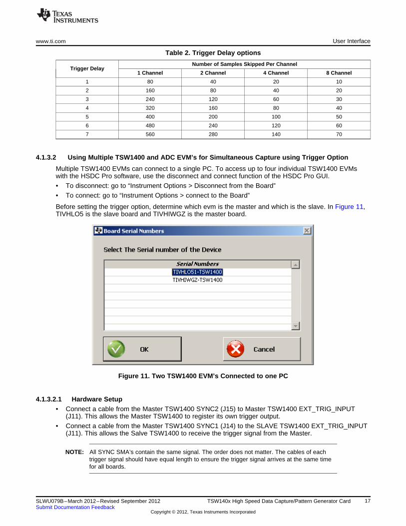
Multiple TSW1400 EVMs can connect to a single PC. To access up to four individual TSW1400 EVMswith the HSDC Pro software, use the disconnect and connect function of the HSDC Pro GUI.
• To disconnect: go to “Instrument Options > Disconnect from the Board”
• To connect: go to “Instrument Options > connect to the Board”
Before setting the trigger option, determine which evm is the master and which is the slave. In Figure 11,TIVHLO5 is the slave board and TIVHIWGZ is the master board.
Figure 11. Two TSW1400 EVM’s Connected to one PC
4.1.3.2.1 Hardware Setup• Connect a cable from the Master TSW1400 SYNC2 (J15) to Master TSW1400 EXT_TRIG_INPUT
(J11). This allows the Master TSW1400 to register its own trigger output.
• Connect a cable from the Master TSW1400 SYNC1 (J14) to the SLAVE TSW1400 EXT_TRIG_INPUT(J11). This allows the Salve TSW1400 to receive the trigger signal from the Master.
NOTE: All SYNC SMA’s contain the same signal. The order does not matter. The cables of eachtrigger signal should have equal length to ensure the trigger signal arrives at the same timefor all boards.
17SLWU079B–March 2012–Revised September 2012 TSW140x High Speed Data Capture/Pattern Generator CardSubmit Documentation Feedback
Copyright © 2012, Texas Instruments Incorporated

User Interface www.ti.com
4.1.3.2.2 Setting up the Slave Board
With the HSDCPro GUI not connected to any of the TSW1400 boards, establish connection to the slaveTSW1400. To set up the slave TSW1400 to accept a trigger signal, go to “data capture options > triggeroption”.
Setup the trigger option as shown in Figure 12. This step arms the TSW1400 slave board to detect triggersignal.
Figure 12. Slave Trigger Setup
Disconnect the TSW1400 slave board from the HSDC Pro GUI. To disconnect, go to “Instrument Options> Disconnect from the Board”.
4.1.3.2.3 Setting up the Master Board
Connect the GUI to the master TSW1400 board. To set up the master TSW1400 to generate a triggersignal, go to “data capture options > trigger option”.
Set up the trigger option as shown in Figure 13. The software trigger sends out a trigger signal upon asoftware GUI button press. This also arms the TSW1400 master board to register its own trigger signal.To capture data using the "Software Trigger enable" option, click on the "Generate Trigger" button on themain panel of the GUI. This will send out a pulse on the SYNC outputs. This signal, which is nowconnected to the EXT_TRG_INPUT of both boards, starts a capture once detected by the FPGA of eachboard.
Figure 13. Master Trigger Setup
18 TSW140x High Speed Data Capture/Pattern Generator Card SLWU079B–March 2012–Revised September 2012Submit Documentation Feedback
Copyright © 2012, Texas Instruments Incorporated
www.ti.com User Interface
4.1.3.2.4 Read Captured Memory from the Slave Board
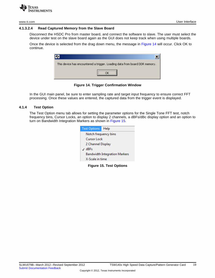
Disconnect the HSDC Pro from master board, and connect the software to slave. The user must select thedevice under test on the slave board again as the GUI does not keep track when using multiple boards.
Once the device is selected from the drag down menu, the message in Figure 14 will occur. Click OK tocontinue.
Figure 14. Trigger Confirmation Window
In the GUI main panel, be sure to enter sampling rate and target input frequency to ensure correct FFTprocessing. Once these values are entered, the captured data from the trigger event is displayed.
4.1.4 Test Option
The Test Option menu tab allows for setting the parameter options for the Single Tone FFT test, notchfrequency bins, Cursor Locks, an option to display 2 channels, a dBFs/dBc display option and an option toturn on Bandwidth Integration Markers as shown in Figure 15.
Figure 15. Test Options
19SLWU079B–March 2012–Revised September 2012 TSW140x High Speed Data Capture/Pattern Generator CardSubmit Documentation Feedback
Copyright © 2012, Texas Instruments Incorporated

User Interface www.ti.com
4.1.4.1 dBFs
When selected, SNR, SFDR, and SINAD results are displayed in dBFs. When not selected, the results aredisplayed in dBc.
4.1.4.2 Notch Frequency Bins
The Notch Frequency Bins option allows the user to remove a number of bins from the SNR calculation ofthe input frequency around the fundamental, DC and a predetermined number of harmonics. The defaultvalues for these settings when the capture is using rectangular mode is 25, 25, 25, and 5, as shown inFigure 16. When the capture mode is set to windowing, the default values are 5, 5, 5, 5.
Figure 16. Notch Frequency Bin removal
By default, the noise calculations for SNR and SINAD are based on the FFT of the captured data with theNotch Filter parameters applied. The first FFT bin at DC is not used because the first bin contains DCoffset and thus does not effect AC parameters or AC performance. The rest of the FFT bins out to theNyquist frequency are included in the calculation of the total noise. There is also an option to notch outbins around a user defined frequency. The default frequency and number of bins is set to 0. If the clockinput is mixing with the input signal, there may be a spur at fs/2 - fin, where fs is the ADC samplefrequency and fin is the input frequency. This option could be used to notch this spur from the results ifdesired. If the user enters a "1" for number of bins to be removed, 1 bin will be removed at the frequencyentered and one bin will be removed from each side of this frequency. If the user enters a "2", the bin atthe frequency will be removed along with 2 bins on each side of the frequency, and so on. The GUIcalculates this frequency for informational use only in the equation box. The default value is "0" since thedefault value of both fs/2 and fin is "0".
20 TSW140x High Speed Data Capture/Pattern Generator Card SLWU079B–March 2012–Revised September 2012Submit Documentation Feedback
Copyright © 2012, Texas Instruments Incorporated

www.ti.com User Interface
4.1.4.3 2 Channel Display and Cursor Lock
If the 2 channel display option is selected, a second data capture display window will open (Figure 17).The user can now use this window to display the same channel but a different parameter, or a differentchannel if a multi-channel ADC is under test. To remove the second channel display and go back to asingle channel display, click on this option again to remove the selected check mark.
Figure 17. Two Channel Display
When 2 channels are displayed, if Cursor lock is enabled, the cursors in the lower display is locked to theones in the upper display.
21SLWU079B–March 2012–Revised September 2012 TSW140x High Speed Data Capture/Pattern Generator CardSubmit Documentation Feedback
Copyright © 2012, Texas Instruments Incorporated

User Interface www.ti.com
4.1.4.4 Bandwidth Integration Markers
Figure 18. Bandwidth Integration Marker Example
When this option is selected, two new markers labeled BIM0 and BIM1 will appear on the FFT plot whenusing the GUI in Single Tone mode only. All of the calculated AC performance statistics in the left columnwill only use the captured values between these bandwidth markers for the calculations. The defaultlocation of marker BIM0 is at 0MHz and marker BIM1 is at ½ the ADC sample rate (Nyquist). The locationof these markers can be set either by entering a frequency value (in Hertz) in the BIM0 and BIM1 locationboxes located in the bottom left corner of the GUI or by clicking on the markers directly and dragging themwith the computer mouse. The AC parameters update immediately after the markers have been moved.Figure 18 shows an example of the Bandwidth Integration Markers being used to display AC parametersinside a 5Mhz bandwidth window centered around a 150 MHz tone that is aliased back to the 50 MHzlocation in the FFT.
4.1.4.5 X-Scale in Time
When using the Time Domain option, the user can change the X-scale of the display from samples to timein µSeconds.
4.1.5 Help
Clicking on the help tab opens a window with four options. The first option, labeled "About", opens astatus window displaying the current version of the GUI, the software DLL, the loaded firmware, and patchversion.
The second option labeled "Debug Support", enables a debug email option. With this option enabled, if aGUI error occurs, the software prompts the user that it is emailing a debug log to a TI support team. Forevery subsequent error until the user disables this feature, the GUI will silently send the log file. The thirdoption, labeled "Check for Updates", will verify if the user's GUI is the latest version available on the TIwebsite.
22 TSW140x High Speed Data Capture/Pattern Generator Card SLWU079B–March 2012–Revised September 2012Submit Documentation Feedback
Copyright © 2012, Texas Instruments Incorporated
www.ti.com User Interface
The fourth option, labeled "EVM GUI Help", opens a window displaying the contents of the User's Guide,allowing the user to search for topics regarding the operation of the GUI.
4.2 Status Windows
The TSW1400 GUI reports system status such as downloading, capturing, warnings, errors, andinformational output in several locations. In the lower right portion of the screen, when the GUI is loadingthe FPGA, loading data to memory, or performing a data capture, a rolling bar will appear in place of theIDLE message. A new window will also open in the middle of the screen describing what the GUI iscurrently doing. An example showing these status windows during a firmware load is shown in Figure 19.
Figure 19. Status Window
During operation of the TSW1400 software, warnings may appear in the center status window if selectionsmade from the drop-down menus of the interface are incompatible with the hardware selections orsettings. For example, if a sample rate is entered that is faster than that supported by a particular ADCdata sheet, a warning appears as shown in Figure 20.
Figure 20. Center Status Window
4.3 Mode Selection
The first selection a user needs to make is to select the type of EVM that is to be tested with theTSW1400 EVM. The user will click on either the “ADC” or “DAC” button located at the top of the GUI asshown in Figure 21.
Figure 21. TSW1400 Modes
The mode selected will determine the main screen format. When ADC is selected, the GUI will be setupfor displaying ADC data capture results. If DAC is selected, the GUI will setup controls to load a testpattern, create a test pattern, and display the graphical representation of the test pattern to be sent to aDAC EVM once the file has been read by the GUI.
23SLWU079B–March 2012–Revised September 2012 TSW140x High Speed Data Capture/Pattern Generator CardSubmit Documentation Feedback
Copyright © 2012, Texas Instruments Incorporated

User Interface www.ti.com
4.4 Device Selection
After the board mode has been set, the user needs to select the device to be tested from the deviceselection drop-down menu. If the GUI is in ADC mode, clicking on the drop down arrow will display theADC options available, as shown in Figure 22. If in DAC mode, the list will display available DAC’s.
Figure 22. ADC Device Selection Window
Each device that has an ini file installed in the proper directory automatically has an entry in the deviceselection drop-down menu.
4.5 Capture Button (ADC Mode only)
The Capture button initiates a data capture once all other selections are made. The data capture can be asingle capture and display, or a continuous repeating capture (Capture option under Data Capture Optiontab in Tool Bar). When continuous capture is enabled, this button display will change from “Capture” to“Stop”. Clicking on this button when in this mode will stop the continuous capture. After a captured hasbeen issued, the GUI will store the setups currently used. If the GUI is closed and then re-opened, most ofthe settings will be restored if the original firmware is still present in the FPGA.
4.6 Test Selection (ADC Mode only)
The Test Selection drop-down has options for displaying data as a Time Domain, Single Tone, Two Tone,or Channel Power, as shown in Figure 23. The Single Tone FFT displays the power spectrum of thecaptured data with calculated AC performance statistics. Time Domain displays the raw captured data inthe format of a logic analyzer display and output level over time. Two tone mode sets up cursors anddisplays results normally used with this type of testing. Channel Power will place cursors around thechannels selected by the user (up to 5) and report the power of each.
24 TSW140x High Speed Data Capture/Pattern Generator Card SLWU079B–March 2012–Revised September 2012Submit Documentation Feedback
Copyright © 2012, Texas Instruments Incorporated

www.ti.com User Interface
Figure 23. Test Selection Drop-Down Options
4.6.1 Single Tone FFT
The Single Tone FFT screen is shown in Figure 24. The larger central pane displays the FFT powerspectrum, whereas the calculated statistics are grouped into categories on the left side of the screen.Settings and inputs relevant to the test are entered in drop-down menus or text input boxes on the bottomleft portion of the window. .
The red horizontal line shown is the RMS line. This line indicates the RMS average of the noise floor ofthe FFT plot. The RMS average is computed over all of the FFT bins except the bin containing the inputfrequency. More precisely, the RMS line = SINAD + FFT Record Length Process Gain where FFT RecordProcess Gain = 10log(number of points/2).
Figure 24. Single Tone FFT Display
25SLWU079B–March 2012–Revised September 2012 TSW140x High Speed Data Capture/Pattern Generator CardSubmit Documentation Feedback
Copyright © 2012, Texas Instruments Incorporated
User Interface www.ti.com
4.6.1.1 Parameter Controls
The sampling rate is entered in the ADC Sampling Rate (Fs) text box. The number is entered in Hertz(Hz), although the letter M may be appended to represent the sampling rate in MHz. For example, 125M =125 MHz or 125,000,000 Hz.
The expected input frequency is entered in the ADC Input Target Frequency text box. If the AutoCalculation of Coherent Input Frequency mode is enabled, then this input frequency is adjusted up ordown slightly away from the input frequency automatically. If coherent input frequency is required, thesignal generator used to source the input frequency must be set to this exact calculated coherentfrequency. The coherent frequency calculation takes the ADC sampling rate, the input frequency asentered by the user in Hertz, and the FFT record length and adjusts the input frequency so that thecaptured data starts and ends on the same place of the sine wave of the input frequency. This avoids anartifact of the FFT calculation from presenting a smeared power spectrum due to the fact that the FFTpresumes the sample of the input is part of a continuous input signal. If the input and sampling frequencyis not coherent, and the sampled data is appended end to end to form a continuous input signal, thenthere is an apparent phase discontinuity at the beginning and the end of the sampled data. Making thesampling and input frequencies coherent avoids this apparent discontinuity. If the input frequency cannotbe made coherent, then the windowing functions other than Rectangular can be used to process out thiseffect to some degree.
The FFT record length can be set in the Analysis Window (samples) text box. The TSW1400EVMsupports FFT analysis lengths of as much as 524288 samples, or as little as 4096 samples. The redvertical line shown in the codes graph represents where the last sample is used from the captured data.The GUI will only allow record lengths that are the same size or smaller than the number of capturedsamples, which is set by the value in the capture option under the Data Capture Options tab. The defaultvalue is 65,536.
4.6.1.2 ADC Captured Data Display Pane
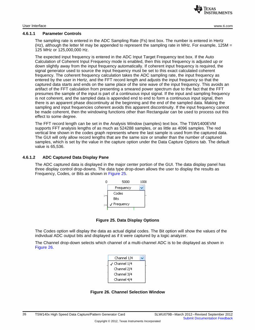
The ADC captured data is displayed in the major center portion of the GUI. The data display panel hasthree display control drop-downs. The data type drop-down allows the user to display the results asFrequency, Codes, or Bits as shown in Figure 25.
Figure 25. Data Display Options
The Codes option will display the data as actual digital codes. The Bit option will show the values of theindividual ADC output bits and displayed as if it were captured by a logic analyzer.
The Channel drop-down selects which channel of a multi-channel ADC is to be displayed as shown inFigure 26.
Figure 26. Channel Selection Window
26 TSW140x High Speed Data Capture/Pattern Generator Card SLWU079B–March 2012–Revised September 2012Submit Documentation Feedback
Copyright © 2012, Texas Instruments Incorporated

www.ti.com User Interface
When in the frequency domain mode, the GUI provides a windowing function to be applied to ADCcaptured data in the Window Display drop-down menu (Figure 27), Rectangular Window applies a unitygain to all data points of the captured data. A Hanning Window, Hamming Window, or Blackman-HarrisWindow function can be applied to the captured data for situations where the sample rate and the inputfrequency are not or cannot be set precisely to capture an integer number of cycles of the input frequency(sometimes called coherent frequency).
Figure 27. Data Windowing Options
4.6.1.3 FFT Power Spectrum
The FFT power spectrum of the captured data is displayed in the major center portion of the window. TheTSW1400 software automatically scales the horizontal axis from DC through the Nyquist frequency,although the scale of the horizontal axis can be changed simply by highlighting the text and typing in anew value. For example, the display in Figure 24 can be used to zoom in on the input frequency byhighlighting the 0 MHz at the end of the spectrum and typing 25M, and then highlighting a value at theother end and typing in 35M. This causes the portion of the power spectrum from 25 MHz through 35 MHzto fill the power spectrum display.
The vertical scale of the power spectrum is automatically scaled to display the noise floor of the FFT resultup through 0 dBFS. The vertical scale can also be manually adjusted by highlighting the limits of thevertical scale and typing in new limits. By default, the first few harmonics of the input frequency aremarked in the display, as well as 2 additional marker, M1 and M2, that can be placed by dragging themarker to any place in the power spectrum, such as a noise spur that is not already marked as aharmonic.
Display properties can be edited by using the mouse to right-click in the power spectrum display. Visibleproperties such as the graph palette or plot legend can be edited, and auto-scale of the vertical andhorizontal axis’s can be enabled or not. The data can also be exported to Excel or a clipboard for copingor processing.
4.6.1.4 Overlay Unwrap Waveform
When in the time domain mode, the Overlay Unwrap Waveform check box, located near the top leftsection of the captured display, allows a calculated normalized waveform to be overlaid (in red) over thesample data waveform (in blue). If the sample and input frequencies are coherent, the sampled data isnormalized into a calculated representation of a single period of a sine wave. Errors in the sampled datafor any reason become immediately apparent as spikes on the unwrapped waveform.
4.6.1.5 Single Tone FFT Statistics
For the Single FFT test, a number of calculated statistics and AC performance measurements aredisplayed to the left of the power spectrum display.
SNR - Signal-to-Noise Ratio is the ratio of the power of the fundamental (PS) or input frequency to thenoise floor power (PN), excluding the power at DC and the first five harmonics. SNR is either given inunits of dBc (dB to carrier) when the absolute power of the fundamental is used as the reference, ordBFS (dB to full scale) when the power of the fundamental is extrapolated to the converter’s full-scalerange.
SNR = 10Log10(Ps/Pn) (1)
SFDR - Spurious-Free Dynamic Range is ratio of the power of the fundamental to the highest otherspectral component (either spur or harmonic). SFDR is typically given in units of dBc (dB to carrier).
27SLWU079B–March 2012–Revised September 2012 TSW140x High Speed Data Capture/Pattern Generator CardSubmit Documentation Feedback
Copyright © 2012, Texas Instruments Incorporated
User Interface www.ti.com
THD - Total Harmonic Distortion is the ratio of the power of the fundamental (PS) to the power in thefirst five harmonics (PD). THD is typically given in data sheets in units of dBc (dB to carrier).SINAD - Signal-to-Noise and Distortion is the ratio of the power of the fundamental (PS) to the powerof all the other spectral components including noise (PN) and distortion (PD), but excluding DC.
SINAD = 10Log10(Ps/(Pn+Pd)) (2)
ENOB - Effective Number of Bits is a measure of a converter’s performance as compared to thetheoretical limit based on quantization noise.
ENOB = (SINAD-1.76)/6.02 (3)
Fund. – This parameter displays the power level of the fundamental.Worst Spur. - This parameter displays the power level of the worst spur.HD2-6 – Display the power values of the second through sixth harmonics of the input frequency in dBc.M1, M2, Delta – Displays the power level of the location of markers M1 and M2. These markers can bemoved around on the spectrum with the mouse. The Delta parameter displays the power differencebetween M2 and M1.
4.6.2 Time Domain
The Time Domain option, when selected, will display the ADC captured data as digital codes in the timedomain. The statistics of the codes reported on the left side of the GUI are minimum value (Min),maximum value (Max), Standard deviation (St. Dev), Mean, Median, RMS, Peak-to-Peak and PAR.
M1, M2, Delta – Displays the code value of the location of markers M1 and M2. These markers can bemoved around on the display with the mouse. The Delta parameter displays the code value differencebetween M2 and M1.
4.6.3 Two Tone
The Two Tone option, when selected, will display a two tone ADC captured with markers placed at thelocations specified by the user. The statistics of the captured data reported on the left side of the GUI areas follows:
F1 - This parameter displays the power level of the first fundamental.F2 - This parameter displays the power level of the second fundamental.2F1+F2 - This parameter displays the power level at the frequency that is equal to twice the firstfundamental plus the second fundamental.2F2+F1 - This parameter displays the power level at the frequency that is equal to twice the secondfundamental plus the first fundamental. The other parameters follow this format.
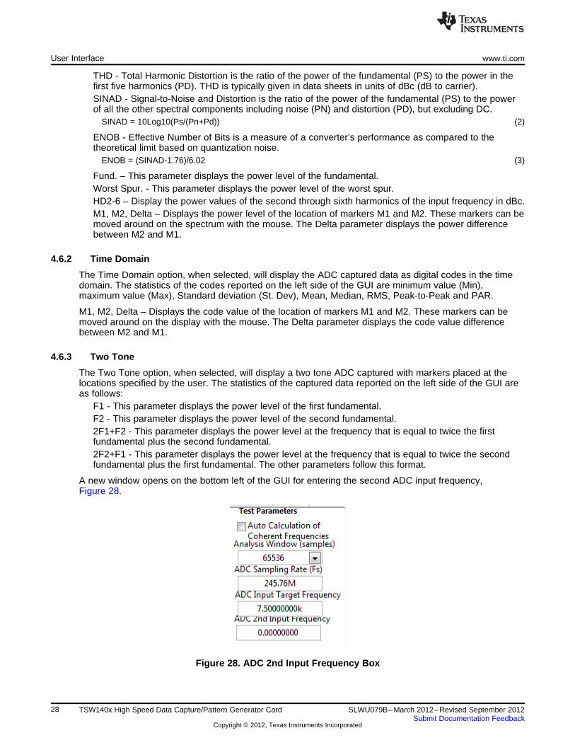
A new window opens on the bottom left of the GUI for entering the second ADC input frequency,Figure 28.
Figure 28. ADC 2nd Input Frequency Box
28 TSW140x High Speed Data Capture/Pattern Generator Card SLWU079B–March 2012–Revised September 2012Submit Documentation Feedback
Copyright © 2012, Texas Instruments Incorporated

www.ti.com User Interface
4.6.4 Channel Power
The Channel Power option, when selected, will display the calculated power of the channels selected inthe parameter column on the left side of the GUI. This option will have three new setting windowsdisplayed in the bottom left of the GUI for the user to select the number of channels (up to 5), the signalwidth, and channel separation of the captured data to be used for channel power measurements. Eachchannel that is selected for a power measurement will have two cursors, one labeled CxL and the otherCxU. The "x" value will indicate the actual channel number. Figure 29 shows an example of a 3 channelpower measurement while using the simulated ADC input function. The input test pattern is called"WCDMA_TM1_complexIF30MHZ_Fdata245.76MHZ_1000.tsw", which is located in the test files directory.
Figure 29. Three Channel Power Measurement Example
29SLWU079B–March 2012–Revised September 2012 TSW140x High Speed Data Capture/Pattern Generator CardSubmit Documentation Feedback
Copyright © 2012, Texas Instruments Incorporated

User Interface www.ti.com
4.7 DAC Display Panel (DAC Mode only)
Selecting the “DAC” button at the top right of the GUI main panel will change the panel display mode forDAC operation as shown in Figure 30.
Figure 30. DAC Display Mode
4.7.1 Send Button (DAC Mode only)
This button, located in the upper left side of the GUI, causes the GUI to download data to the TSW1400on-board memory, followed by the TSW1400 sending data from the memory module to the DAC EVMunder test. This button is only active after valid data has been loaded into the PC memory by the GUI.
4.7.2 Load File to transfer into TSW1400 Button
The button labeled “Load File to transfer into TSW1400” is used to select the test pattern file to be loadedinto the board memory. Clicking on this button opens a navigator which the user will use to select thedesired test file. The format of the test file can be either .csv or .tsw. Once selected, the file will be loadedinto the PC memory used by the GUI.
The imported file must be text format integer value from -32768 to 32767 in a single column format iftesting a single DAC. For dual DAC’s, the file must be in 2 columns. For quad DAC’s, 4 columns. Thelength can be from 4096 to 512M (single column) in increments of 32. The GUI comes with severalexample test files that can be found under the following directory: C:\Program Files\TexasInstruments\High Speed Data Converter Pro\TSW1400 Details\Test files.
30 TSW140x High Speed Data Capture/Pattern Generator Card SLWU079B–March 2012–Revised September 2012Submit Documentation Feedback
Copyright © 2012, Texas Instruments Incorporated

www.ti.com User Interface
4.7.3 Parameter Controls
Four parameters are used with the data file to generate the Time and Frequency domain plots.Preamble – The number of samples before the loop starting point (default is 0). This value must be inincrements of 32.Data Rate – Sample rate of I/Q samples of the test file. This is only used by the GUI FFT frequencydisplay graph. The number is entered in Hertz (Hz), although the letter M may be appended torepresent the sampling rate in MHz.DAC Option – Determines if the test pattern file is either 2's Compliment or Offset Binary.Active Channel – Selects the channel in the test pattern file that is displayed (1, 2, 3, or 4).
After a file has been loaded and the parameters updated, the GUI panel will present a graphicalrepresentation of the data. An example of an Offset Binary, 25.1 MHz tone with a data rate of 250 MHz isshown in Figure 31.
Figure 31. DAC Test Pattern Display
The “Send” button will now became active. Clicking on this button will start the transfer of data from theTSW1400 to a DAC EVM under test. This pattern is a looping test pattern that constantly runs until thesend button is clicked on again.
Every time the pattern starts over, a sync pulse will be generated on the SMA labeled "SYNC4". Thisactive high pulse width will be 8 sample clock cycles wide. The SMA labeled "SYNC3" will have a clockthat is the sample rate divided by 16. These signals can be used to trigger external test equipment suchas a spectrum analyzer.
31SLWU079B–March 2012–Revised September 2012 TSW140x High Speed Data Capture/Pattern Generator CardSubmit Documentation Feedback
Copyright © 2012, Texas Instruments Incorporated

ADC Data Capture Software Operation www.ti.com
4.8 I/Q Multi-tone Generator
Located in the lower left corner of the GUI is an I/Q Multi-tone Generator tool that allows the user togenerate test patterns that can be used with the TSW1400 GUI. The following parameters are used withthis tool:
Tone BW – Tone bandwidth in Hertz. For Megahertz, enter a "M" after the number.# - Number of tones. If set to 1, Tone BW will be ignored.Tone Center – Center frequency of tones in Hertz.# of Samples – Number of test samples. 4096 to 2M, in increments of 32.Tone Selection – Real or I/Q.Scaling Factor (1X) – From full scale output. 0.0000 to 1.0000.
To generate a pattern, enter the desired parameters then click on the button labeled “Create Tones”. Clickon “Send” will send the data to the TSW1400 memory then to the DAC EVM under test. An option exist toallow the user to save this file as well.
5 ADC Data Capture Software Operation
5.1 Testing with an ADS5281 EVM
This section describes the operation when testing with an ADS5281 EVM that has a LVDS outputinterface.
• Power down the TSW1400 if an ADC evm is not installed.
• Connect J8 of the ADS5281 EVM to connector J3 of the TSW1400.
• Provide unpowered +5 VDC connections to J1 and return to J2 of the ADS5281 EVM.
• Provide a 1.5 VPP 40 MHz sine-wave clock to J26 of the ADS5281 EVM.
• Provide a filter 5.1 MHz analog input to CH1.
• Power up the TSW1400 followed by the ADC evm.
• Start up the TSW1400 GUI as described in the Software Start Up section.
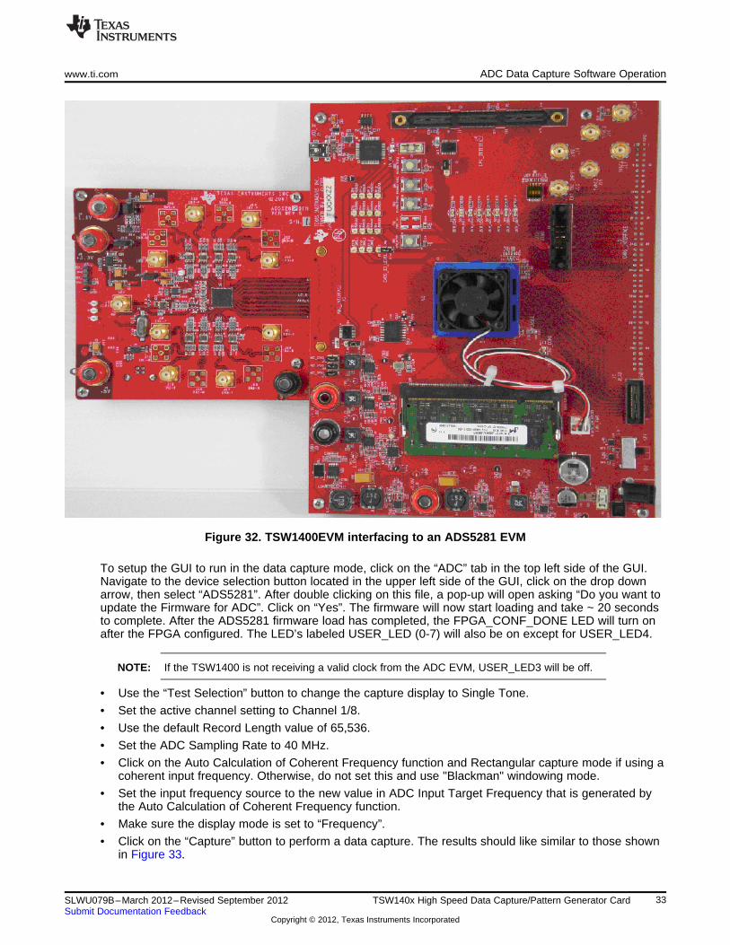
• The TSW1400 EVM connected to an ADS5281 EVM is shown in Figure 32
32 TSW140x High Speed Data Capture/Pattern Generator Card SLWU079B–March 2012–Revised September 2012Submit Documentation Feedback
Copyright © 2012, Texas Instruments Incorporated
www.ti.com ADC Data Capture Software Operation
Figure 32. TSW1400EVM interfacing to an ADS5281 EVM
To setup the GUI to run in the data capture mode, click on the “ADC” tab in the top left side of the GUI.Navigate to the device selection button located in the upper left side of the GUI, click on the drop downarrow, then select “ADS5281”. After double clicking on this file, a pop-up will open asking “Do you want toupdate the Firmware for ADC”. Click on “Yes”. The firmware will now start loading and take ~ 20 secondsto complete. After the ADS5281 firmware load has completed, the FPGA_CONF_DONE LED will turn onafter the FPGA configured. The LED’s labeled USER_LED (0-7) will also be on except for USER_LED4.
NOTE: If the TSW1400 is not receiving a valid clock from the ADC EVM, USER_LED3 will be off.
• Use the “Test Selection” button to change the capture display to Single Tone.
• Set the active channel setting to Channel 1/8.
• Use the default Record Length value of 65,536.
• Set the ADC Sampling Rate to 40 MHz.
• Click on the Auto Calculation of Coherent Frequency function and Rectangular capture mode if using acoherent input frequency. Otherwise, do not set this and use "Blackman" windowing mode.
• Set the input frequency source to the new value in ADC Input Target Frequency that is generated bythe Auto Calculation of Coherent Frequency function.
• Make sure the display mode is set to “Frequency”.
• Click on the “Capture” button to perform a data capture. The results should like similar to those shownin Figure 33.
33SLWU079B–March 2012–Revised September 2012 TSW140x High Speed Data Capture/Pattern Generator CardSubmit Documentation Feedback
Copyright © 2012, Texas Instruments Incorporated

ADC Data Capture Software Operation www.ti.com
Figure 33. ADC5281 Single Tone FFT Capture Results
The user can now change other parameters and do another capture to observe the ADC outputs withdifferent frequencies, amplitudes, and in other formats such as codes, or bits.
After the firmware is loaded, if the user clicks the drop down arrow in the device selection window, the GUIwill indicate which ADC EVM’s can be used with this firmware load by adding a black diamond in front ofthe device name, as shown in Figure 34. If the user does not power down the TSW1400, any one of thedevices with a black diamond can be tested without doing another firmware load.
34 TSW140x High Speed Data Capture/Pattern Generator Card SLWU079B–March 2012–Revised September 2012Submit Documentation Feedback
Copyright © 2012, Texas Instruments Incorporated

www.ti.com ADC Data Capture Software Operation
Figure 34. Devices Supported with Current GUI
WARNINGAfter testing is completed, always close the GUI beforedisconnecting the USB cable between the host PC and EVM.Failure to do this can cause a blue screen reboot to occur on thehost PC.
5.2 Testing with an ADS62P49EVM CMOS Interface
This section describes the operation when testing with an ADS62P49EVM that is configured for CMOSoutput interface.
• Power down the TSW1400 if an ADC evm is not installed.
• Connect J1 and J2 of the ADS62P49EVM to connector J1 of the TSW1400EVM.
NOTE: Pin 1 of the TSW1400 connector plugs into pin 39 of J1 on the ADS62P49EVM.
• Provide unpowered +5 VDC connections to J10 and return to J12 of the ADS62P49EVM.
• Provide a 1.5 VPP 150 MHz sine-wave clock to J19 of the ADS62P49EVM. Make sure this clock iswithin the frequency limits specified in the data sheet when operating in CMOS mode.
• Provide a filtered 5.1 MHz analog input to CH1 (J6).
• Power up the TSW1400 followed by the ADC EVM.
• Setup the ADS62P49EVM to operate in parallel mode, offset binary parallel CMOS output, and internalreference.
• Start up the TSW1400 GUI as described in the Software Start Up section.
35SLWU079B–March 2012–Revised September 2012 TSW140x High Speed Data Capture/Pattern Generator CardSubmit Documentation Feedback
Copyright © 2012, Texas Instruments Incorporated
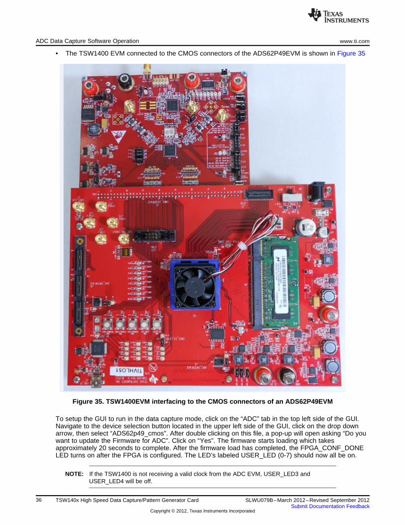
ADC Data Capture Software Operation www.ti.com
• The TSW1400 EVM connected to the CMOS connectors of the ADS62P49EVM is shown in Figure 35
Figure 35. TSW1400EVM interfacing to the CMOS connectors of an ADS62P49EVM
To setup the GUI to run in the data capture mode, click on the “ADC” tab in the top left side of the GUI.Navigate to the device selection button located in the upper left side of the GUI, click on the drop downarrow, then select “ADS62p49_cmos”. After double clicking on this file, a pop-up will open asking “Do youwant to update the Firmware for ADC”. Click on “Yes”. The firmware starts loading which takesapproximately 20 seconds to complete. After the firmware load has completed, the FPGA_CONF_DONELED turns on after the FPGA is configured. The LED’s labeled USER_LED (0-7) should now all be on.
NOTE: If the TSW1400 is not receiving a valid clock from the ADC EVM, USER_LED3 andUSER_LED4 will be off.
36 TSW140x High Speed Data Capture/Pattern Generator Card SLWU079B–March 2012–Revised September 2012Submit Documentation Feedback
Copyright © 2012, Texas Instruments Incorporated

www.ti.com ADC Data Capture Software Operation
• Use the “Test Selection” button to change the capture display to Single Tone.
• Set the active channel setting to Channel 1/2.
• Use the default Record Length value of 65,536.
• Set the ADC Sampling Rate to 150 MHz.
• Click on the Auto Calculation of Coherent Frequency function and Rectangular capture mode if using acoherent input frequency. Otherwise, do not set this and use "Blackman" windowing mode.
• Set the input frequency source to the new value in ADC Input Target Frequency that is generated bythe Auto Calculation of Coherent Frequency function.
• Make sure the display mode is set to “Frequency”.
• Click on the “Capture” button to perform a data capture. The results should like similar to those shownin Figure 36
Figure 36. TSW1400EVM Captured Results from ADS62P49EVM
37SLWU079B–March 2012–Revised September 2012 TSW140x High Speed Data Capture/Pattern Generator CardSubmit Documentation Feedback
Copyright © 2012, Texas Instruments Incorporated
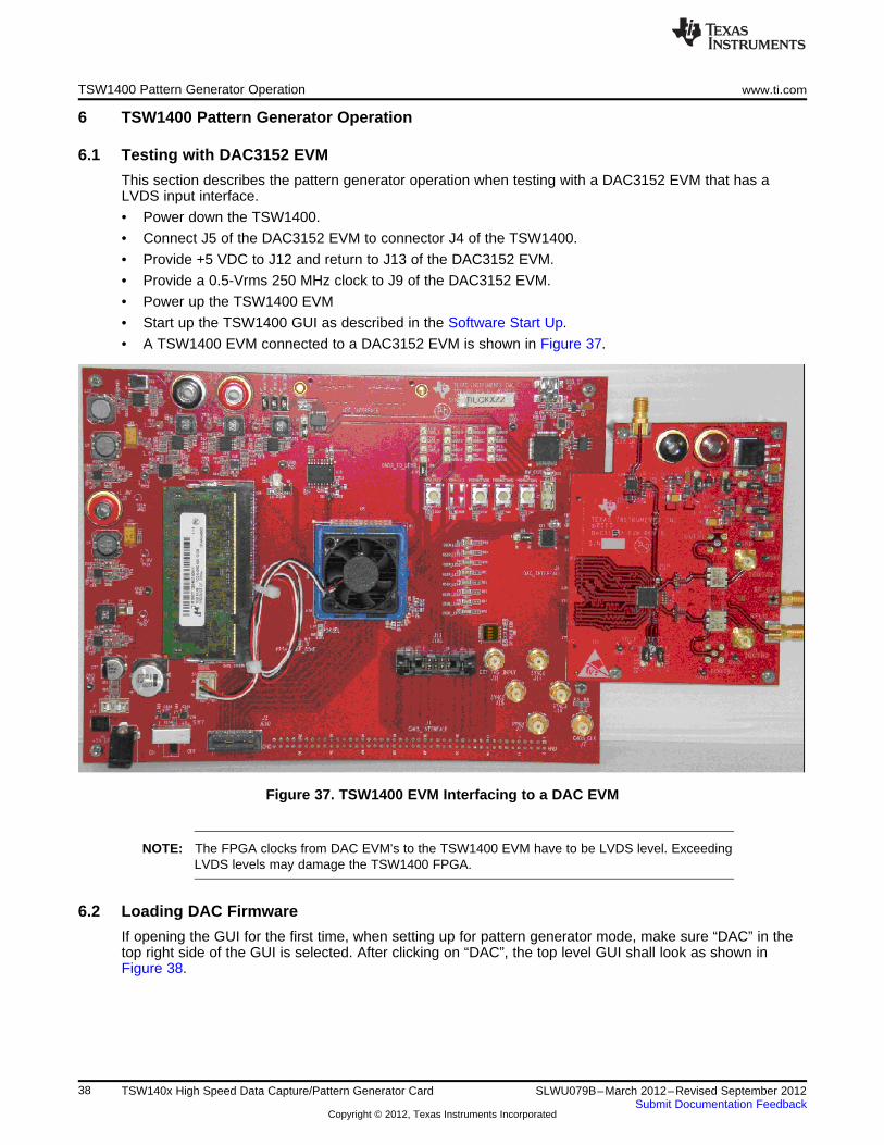
TSW1400 Pattern Generator Operation www.ti.com
6 TSW1400 Pattern Generator Operation
6.1 Testing with DAC3152 EVM
This section describes the pattern generator operation when testing with a DAC3152 EVM that has aLVDS input interface.
• Power down the TSW1400.
• Connect J5 of the DAC3152 EVM to connector J4 of the TSW1400.
• Provide +5 VDC to J12 and return to J13 of the DAC3152 EVM.
• Provide a 0.5-Vrms 250 MHz clock to J9 of the DAC3152 EVM.
• Power up the TSW1400 EVM
• Start up the TSW1400 GUI as described in the Software Start Up.
• A TSW1400 EVM connected to a DAC3152 EVM is shown in Figure 37.
Figure 37. TSW1400 EVM Interfacing to a DAC EVM
NOTE: The FPGA clocks from DAC EVM’s to the TSW1400 EVM have to be LVDS level. ExceedingLVDS levels may damage the TSW1400 FPGA.
6.2 Loading DAC Firmware
If opening the GUI for the first time, when setting up for pattern generator mode, make sure “DAC” in thetop right side of the GUI is selected. After clicking on “DAC”, the top level GUI shall look as shown inFigure 38.
38 TSW140x High Speed Data Capture/Pattern Generator Card SLWU079B–March 2012–Revised September 2012Submit Documentation Feedback
Copyright © 2012, Texas Instruments Incorporated

www.ti.com TSW1400 Pattern Generator Operation
Figure 38. TSW1400EVM GUI DAC Mode Top Level
To run the GUI in DAC pattern generator mode, the FPGA must be loaded with the proper firmware, whichis determined by the DAC type to be tested.
In the “Select DAC” button of the GUI, click on the drop down arrow and select the DAC3152 (Figure 39).This will be the targeted EVM for this test example.
Figure 39. DAC Selection
Click on “Yes” when asked “Do you want to update the firmware for DAC”. The firmware for this setup willnow be loaded during this process, which will take approximately 20 seconds. After the firmware load hascompleted, the LED’s labeled USER_LED (0-7) will now turn on except for USER_LED 3 and 5.USER_LED 3 is used to indicate the status of a second PLL, which is not used with this firmware build,and USER_LED 5 indicates if there is a FIFO overflow (error) of the transmit data.
39SLWU079B–March 2012–Revised September 2012 TSW140x High Speed Data Capture/Pattern Generator CardSubmit Documentation Feedback
Copyright © 2012, Texas Instruments Incorporated
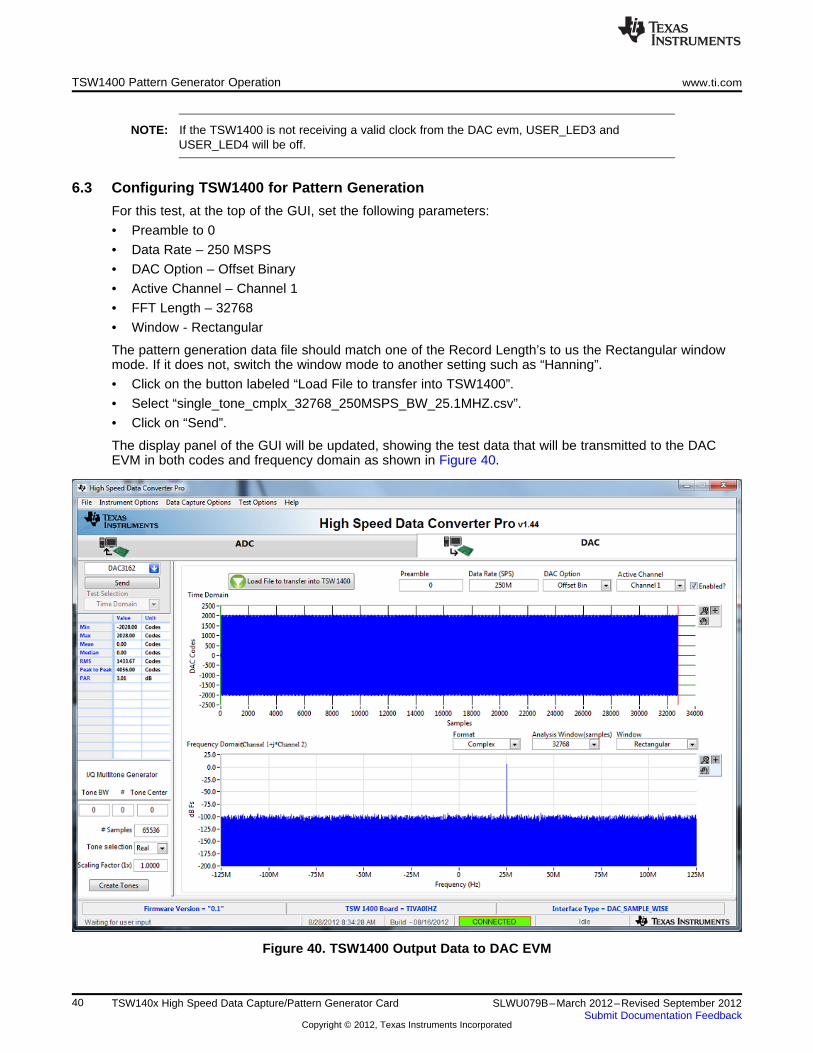
TSW1400 Pattern Generator Operation www.ti.com
NOTE: If the TSW1400 is not receiving a valid clock from the DAC evm, USER_LED3 andUSER_LED4 will be off.
6.3 Configuring TSW1400 for Pattern Generation
For this test, at the top of the GUI, set the following parameters:
• Preamble to 0
• Data Rate – 250 MSPS
• DAC Option – Offset Binary
• Active Channel – Channel 1
• FFT Length – 32768
• Window - Rectangular
The pattern generation data file should match one of the Record Length’s to us the Rectangular windowmode. If it does not, switch the window mode to another setting such as “Hanning”.
• Click on the button labeled “Load File to transfer into TSW1400”.
• Select “single_tone_cmplx_32768_250MSPS_BW_25.1MHZ.csv”.
• Click on “Send”.
The display panel of the GUI will be updated, showing the test data that will be transmitted to the DACEVM in both codes and frequency domain as shown in Figure 40.
Figure 40. TSW1400 Output Data to DAC EVM
40 TSW140x High Speed Data Capture/Pattern Generator Card SLWU079B–March 2012–Revised September 2012Submit Documentation Feedback
Copyright © 2012, Texas Instruments Incorporated

www.ti.com TSW1400 Pattern Generator Operation
Using a spectrum analyzer, verify that there is now a 25.1 MHz tone present on both SMA J2 (IOUTA2)and J3 (IOUTB2) of the DAC3152 EVM.
To shut down the GUI, click on the “File” tab in the upper right corner of the GUI and select “Exit” in thepop up window that opens. This will specify that the USB ports are released by the software.
6.4 Testing with a DAC5688EVM CMOS Interface
This section describes the operation when testing with a DAC5688EVM that has a CMOS input interface.
• Power down the TSW1400 if the DAC5688EVM is not installed.
NOTE: J1 pin 1 of the TSW1400 connector plugs into J2 pin 1 on the DAC5688EVM
• Provide unpowered +3.3 VDC connections to J15 and return to J16 of the DAC5688EVM.
• Provide unpowered +1.8 VDC connections to J13 and return to J14 of the DAC5688EVM.
• Provide a USB cable between the DAC5688EVM and a host PC.
• Provide an external sinewave source at 491.52 MHz with a 1-Vrms, 0-V offset to SMA J20(EXT_VCXO) of the DAC5688EVM.
• Connect a SMA cable from OUTCLK3 connector (J17) of the DAC5688EVM to CMOS_CLK (J7) of theTSW1400EVM.
• Power up the TSW1400 followed by the DAC evm.
• Load and start up the DAC5688EVM GUI as described in the DAC5688EVM User’s Guide. Thesoftware and User’s Guide can be found at http://www.ti.com/tool/dac5688evm.
• Start up the TSW1400 GUI as described in the Software Start Up section.
• The TSW1400EVM connected to the CMOS connectors of the DAC5688EVM is shown in Figure 41
41SLWU079B–March 2012–Revised September 2012 TSW140x High Speed Data Capture/Pattern Generator CardSubmit Documentation Feedback
Copyright © 2012, Texas Instruments Incorporated

TSW1400 Pattern Generator Operation www.ti.com
Figure 41. TSW1400EVM Interfacing to the CMOS Connectors of a DAC5688EVM
Using the DAC5688EVM GUI, load the EVM with the test file called “example”. This can be found atC:\Program Files\Texas Instruments\DAC5688\DAC5688 Configuration Files. This sets up the DAC5688to receive a WCDMA test pattern from the TSW1400 with a data rate of 122.88MHz. CLK2 of DAC5688operates at 491.52 MHz and the DAC interpolation is set to 4x, requiring the input data rate to be at122.88MHz.
In the DAC5688 GUI, go to the CDCM7005 tab and set the Y3 Output (OUTCLK3) to divide by 4,LVCMOS, and inverting per Figure 42.
42 TSW140x High Speed Data Capture/Pattern Generator Card SLWU079B–March 2012–Revised September 2012Submit Documentation Feedback
Copyright © 2012, Texas Instruments Incorporated

www.ti.com TSW1400 Pattern Generator Operation
Figure 42. CDCM7005 tab on DAC5688 GUI
This generates an inverted 122.88MHz clock used by the TSW1400 to generate the CMOS test pattern.
NOTE: The CMOS data rate for the TSW1400EVM should never exceed 250 MHz. This rate is setby the CMOS_CLOCK input provide to J7. When operating at frequencies near this limit, theuser may need to adjust the delay of this signal to meet the timing specs of the DAC undertest.
On the DAC5688EVM, there is an option to use a spare output of the CDCM7005 clockgenerator as a clock source. In this example, the OUTCLK3 of the CDCM7005 is inverted foroptimized setup and hold time. Another way to adjust the delay is to use different cablelengths for this clock source.
If opening the TSW1400 GUI for the first time, when setting up for pattern generator mode, make sure“DAC” in the top right side of the GUI is selected. This targets the EVM for this test example. In the “SelectDAC” button of the GUI, click on the drop down arrow and select “cmos”. This firmware is used by mostHigh Speed CMOS DAC EVM’s.
Click on “Yes” when asked “Do you want to update the firmware for DAC”. The firmware setup is loadedduring this process, which takes approximately 20 seconds. After the firmware load has completed, theLED’s labeled USER_LED (0-7) will now turn on except for USER_LED 5. USER_LED 3 is used toindicate the status of a second PLL, and USER_LED 5 indicates if there is a FIFO overflow (error) of thetransmit data.
NOTE: If the TSW1400 is not receiving a valid clock from the DAC EVM, USER_LED3 andUSER_LED4 are off.
43SLWU079B–March 2012–Revised September 2012 TSW140x High Speed Data Capture/Pattern Generator CardSubmit Documentation Feedback
Copyright © 2012, Texas Instruments Incorporated

TSW1400 Pattern Generator Operation www.ti.com
6.4.1 For this test, at the top of the GUI, set the following parameters:
• Preamble to 0
• Data Rate – 122.88M (MSPS)
• DAC Option – 2’s Comp
• Active Channel – Channel 1
• Click on the button labeled “Load File to transfer into TSW1400”.
• Select “WCDMA_TM1_complexIF30MHz_Fdata122.88MHz_1000.csv”.
• Click on “Send”.
The display panel of the GUI is updated, showing the test data that is transmitted to the DAC EVM in bothcodes and frequency domain as shown in Figure 43.
Figure 43. GUI After Test File Loaded
If the DAC5688EVM is configured for IF output, connect a spectrum analyzer to either SMA J4 (IOUTB2)or J9 (IOUTA2) of the EVM. The DAC example file has a NCO setting of 61.44 MHz and the test patternIF is centered at 30 MHz. The signal should be a single carrier centered around 91.44 MHz, as shown inFigure 44.
NOTE: The DAC5688EVM has the default setup as RF output. The modulator output location will beat the LO frequency plus 91.44 MHz. For details about IF and RF output configurationsettings, see section 4.7 of the DAC5688EVM User’s Guide (SLAU241).
44 TSW140x High Speed Data Capture/Pattern Generator Card SLWU079B–March 2012–Revised September 2012Submit Documentation Feedback
Copyright © 2012, Texas Instruments Incorporated

www.ti.com TSW1405 Functional Description
Figure 44. DAC5688 IF Output
7 TSW1405 Functional Description
The TSW1405 Capture Card is a lower cost capture card than the TSW1400, with reduced memorycapacity for storing samples captured from TI High Speed ADC EVMs. The TSW1405 has a Samtecconnector to directly connect to the LVDS data bus from the EVM. The TSW1400 does not haveconnections for CMOS ADC EVMs. The TSW1405 uses the same software GUI as the TSW1400.
The TSW1405 does not have an EEPROM resident on the board to hold an FPGA bit file, but rather willget the bit file downloaded from the software GUI running on a PC at runtime. In this manner theTSW1405 will not need to be reprogrammed when new ADC EVMs or additional capture features becomeavailable. The planned FPGA firmware upgrades consists of new files to be downloaded to the softwareGUI. The TSW1405 does have a footprint for a firmware EEPROM to be installed, if desired.
45SLWU079B–March 2012–Revised September 2012 TSW140x High Speed Data Capture/Pattern Generator CardSubmit Documentation Feedback
Copyright © 2012, Texas Instruments Incorporated
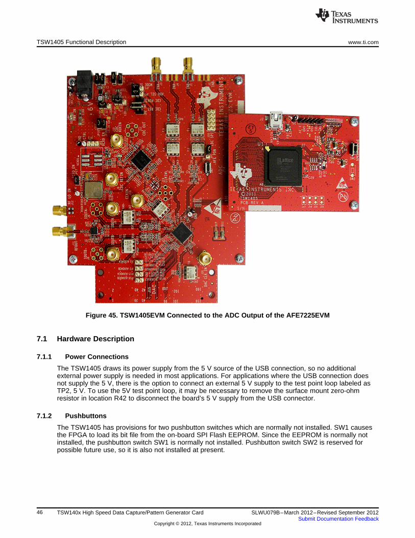
TSW1405 Functional Description www.ti.com
Figure 45. TSW1405EVM Connected to the ADC Output of the AFE7225EVM
7.1 Hardware Description
7.1.1 Power Connections
The TSW1405 draws its power supply from the 5 V source of the USB connection, so no additionalexternal power supply is needed in most applications. For applications where the USB connection doesnot supply the 5 V, there is the option to connect an external 5 V supply to the test point loop labeled asTP2, 5 V. To use the 5V test point loop, it may be necessary to remove the surface mount zero-ohmresistor in location R42 to disconnect the board’s 5 V supply from the USB connector.
7.1.2 Pushbuttons
The TSW1405 has provisions for two pushbutton switches which are normally not installed. SW1 causesthe FPGA to load its bit file from the on-board SPI Flash EEPROM. Since the EEPROM is normally notinstalled, the pushbutton switch SW1 is normally not installed. Pushbutton switch SW2 is reserved forpossible future use, so it is also not installed at present.
46 TSW140x High Speed Data Capture/Pattern Generator Card SLWU079B–March 2012–Revised September 2012Submit Documentation Feedback
Copyright © 2012, Texas Instruments Incorporated

www.ti.com TSW1405 Functional Description
7.1.3 Jumpers
The TSW1405 has provisions for four jumpers which are normally not installed. Each jumper has one postconnected to an FPGA input and a pull up resistor while the other post connects to ground. Thesejumpers are reserved for possible future use for setting options to the FPGA or for possible outputconnections from the FPGA.
The TSW1405 also has an optional 6-pin header for connection to the JTAG port of the FPGA, but theJTAG header may not be installed. The JTAG port would allow the use of an FPGA programming pod, butis not necessary since the FPGA firmware is downloaded from the PC at runtime.
7.1.4 LEDs
The TSW1405 has an LED labeled D1 Done that is lit when the FPGA is finished loading a bit file and isready for use. An additional LED labeled D2 is normally not installed and is reserved for future use. Forthe initial release of the TSW1405, the LED D2 (if installed) will flash when an LVDS clock is present fromthe ADC EVM.
7.2 Software Operation
The TSW1405 uses the same software GUI as the TSW1400, providing for a consistent and familiarexperience for the user of the TI Capture Cards. When the GUI is launched on the PC, the GUI will detectwhether any TSW1400 or TSW1405 capture cards are connected to the PC USB ports, and allow the userto select which to connect to if there are more than one connected.
47SLWU079B–March 2012–Revised September 2012 TSW140x High Speed Data Capture/Pattern Generator CardSubmit Documentation Feedback
Copyright © 2012, Texas Instruments Incorporated

TSW1405 Functional Description www.ti.com
7.2.1 Channel Selection
Because the TSW1405 has limited memory for sample capture, the GUI makes provision for selecting thenumber of channels from which to capture samples. This is a feature in the GUI that is not needed for theTSW1400, so there is a GUI popup dialog box for the TSW1405 that is not used for the TSW1400, asshown in Figure 46.
If a device is selected in the GUI that has more than one channel available, the Channel Selection Dialogwindow will let the user select one or more channels to be used for capture. If two, four or eight channelsare selected, then samples from those channels are captured into the capture memory simultaneously.
Figure 46. Number of Channels Selection
The TSW1405 has enough internal memory in the FPGA to capture as many as 65536 samples of 16bitdata. The 65536 samples will be automatically allocated to one, two, four or eight channels depending onthe channel selections set in the GUI. If one channel is selected for capture, then the record length for thatchannel will be 65536 samples. If two channels are selected for capture, then each channel will get arecord length of 32768 samples. Four channels will cause a record length of 16384 samples to becaptured for each channel, and eight channels will capture 8192 samples for each channel.
48 TSW140x High Speed Data Capture/Pattern Generator Card SLWU079B–March 2012–Revised September 2012Submit Documentation Feedback
Copyright © 2012, Texas Instruments Incorporated

www.ti.com TSW1406 Functional Description
8 TSW1406 Functional Description
The TSW1406 Pattern Generator Card is a low cost pattern generator card with reduced memory capacityfor providing test patterns to TI High Speed DAC EVMs. The TSW1406 has a High Speed Samtecconnector that directly connects to the LVDS input data bus of DAC EVM. The TSW1406 does not haveconnections for CMOS DAC EVMs. The TSW1406 uses the same software GUI as the TSW1400.
The TSW1406 does not have an EEPROM resident on the board to hold an FPGA bit file, but rather willget the bit file downloaded from the software GUI running on a PC at runtime. In this manner theTSW1406 will not need to be reprogrammed when new DAC EVMs or additional capture features becomeavailable. The planned FPGA firmware upgrades consists of new files to be downloaded to the softwareGUI. The TSW1406 does have a footprint for a firmware EEPROM to be installed, if desired.
Figure 47. TSW1406EVM Connected to the DAC input of the AFE7225EVM
8.1 Hardware Description
8.1.1 Power Connections
The TSW1406 draws its power supply from the 5 V source of the USB connection, so no additionalexternal power supply is needed in most applications. For applications where the USB connection doesnot supply the 5 V, there is the option to connect an external 5V supply to the test point loop labeled asTP2 and GND to TP1. To use the 5 V test point loop, make sure to remove R42 to disconnect the board’s5 V supply from the USB connector.
8.1.2 Pushbuttons
The TSW1406 has provisions for two pushbutton switches. SW1 causes the FPGA to load its bit file fromthe on-board SPI Flash EEPROM. This mode is currently not supported. Pushbutton switch SW2 isreserved for possible future use.
49SLWU079B–March 2012–Revised September 2012 TSW140x High Speed Data Capture/Pattern Generator CardSubmit Documentation Feedback
Copyright © 2012, Texas Instruments Incorporated
Revision History www.ti.com
8.1.3 Jumpers
The TSW1406 has provisions for four jumpers which are normally not installed. Each jumper has one postconnected to an FPGA input and a pull up resistor while the other post connects to ground. Thesejumpers are reserved for possible future use for setting options to the FPGA or for possible outputconnections from the FPGA. The TSW1406 also has an optional 6-pin header for connection to the JTAGport of the FPGA. The JTAG port would allow the use of an FPGA programming pod, but is not necessarysince the FPGA firmware is downloaded from the PC at runtime.
8.1.4 LEDs
The TSW1406 LED labeled D1 is the “Done” indicator of the FPGA. This LED is lit when the FPGA isfinished loading a bit file and is ready for use. An additional LED labeled D2 represents PLL lock status ofthe FPGA which should be on for normal operation.
8.2 Software Operation
The TSW1406 uses the same software GUI as the TSW1400, providing for a consistent and familiarexperience for the user of the TI Pattern Generator Cards. When the GUI is launched on the PC, the GUIdetects whether any TSW1400 or TSW1406 capture cards are connected to the PC USB ports, and allowthe user to select which to connect to if there are more than one connected.
9 Revision History
Revision A (March 2012)
Changed and Added figures and text throughout the document
Added section 7 - TSW1405 Functional Description
Revision B (September 2012)
The GUI supports the TSW1406 Low Cost pattern Generation card in addition to the TSW1400 and TSW1405.
Master and slave triggering modes are available for the TSW1400. Under 'Data Capture Option' there is now a 'Trigger Option'menu with two sub-options. 'Trigger Mode Enable' allows externally triggering capture into DDR memory through SMA connectornamed 'EXT_TRG_IN' while 'Software Trigger' generates a trigger on the four SMA connectors labeled 'SYNC'
Added FFT Averaging feature (with or without continuous capture). This feature performs 'n' continuous captures (max = 10) andaverages the FFT's on the fly to reduce noise
Complex FFT feature is now available for the DAC panel. The 'format' dropdown above the FFT plot controls whether the FFT isvisualized in real or complex mode.
Includes ‘DAC channel enable’ feature that allows one to selectively send zeroes to selected DAC channels
Increased speed of Continuous Capture function.
The notch frequency bins menu option is disabled in all modes except single tone.
Revised defaults for notch filters ( 25:25:25) in windowed modes only. Rectangular window modes filter parameters unchanged.
Peak to Peak amplitude and PAR values are now displayed for time domain DAC and ADC.
FFT plot in DAC mode defaults to windowed (Blackman window) mode when creating tone or loading file with >64K samples.
The Time domain plot color is now dark blue (both on the context plot and main plots).
Test Options tab added option to display the X axis scale in "time" instead of "Samples".
The Bandwidth Integration Markers could earlier be swapped, causing problems. Now they cannot.
GUI auto-disconnects gracefully if the USB cable is unplugged and some user operation is attempted.
GUI includes a "Check for Updates" feature that checks (every 7 days) for latest version and prompts a download if a newerversion is available for download at the TI product page. Feature is also accessible from menu.
Advanced "FFT x scale" feature in Device INI to adjust the FFT x scale for decimated sample rate devices.
50 TSW140x High Speed Data Capture/Pattern Generator Card SLWU079B–March 2012–Revised September 2012Submit Documentation Feedback
Copyright © 2012, Texas Instruments Incorporated

EVALUATION BOARD/KIT/MODULE (EVM) ADDITIONAL TERMS
Texas Instruments (TI) provides the enclosed Evaluation Board/Kit/Module (EVM) under the following conditions:
The user assumes all responsibility and liability for proper and safe handling of the goods. Further, the user indemnifies TI from all claimsarising from the handling or use of the goods.
Should this evaluation board/kit not meet the specifications indicated in the User’s Guide, the board/kit may be returned within 30 days fromthe date of delivery for a full refund. THE FOREGOING LIMITED WARRANTY IS THE EXCLUSIVE WARRANTY MADE BY SELLER TOBUYER AND IS IN LIEU OF ALL OTHER WARRANTIES, EXPRESSED, IMPLIED, OR STATUTORY, INCLUDING ANY WARRANTY OFMERCHANTABILITY OR FITNESS FOR ANY PARTICULAR PURPOSE. EXCEPT TO THE EXTENT OF THE INDEMNITY SET FORTHABOVE, NEITHER PARTY SHALL BE LIABLE TO THE OTHER FOR ANY INDIRECT, SPECIAL, INCIDENTAL, OR CONSEQUENTIALDAMAGES.
Please read the User's Guide and, specifically, the Warnings and Restrictions notice in the User's Guide prior to handling the product. Thisnotice contains important safety information about temperatures and voltages. For additional information on TI's environmental and/or safetyprograms, please visit www.ti.com/esh or contact TI.
No license is granted under any patent right or other intellectual property right of TI covering or relating to any machine, process, orcombination in which such TI products or services might be or are used. TI currently deals with a variety of customers for products, andtherefore our arrangement with the user is not exclusive. TI assumes no liability for applications assistance, customer product design,software performance, or infringement of patents or services described herein.
REGULATORY COMPLIANCE INFORMATION
As noted in the EVM User’s Guide and/or EVM itself, this EVM and/or accompanying hardware may or may not be subject to the FederalCommunications Commission (FCC) and Industry Canada (IC) rules.
For EVMs not subject to the above rules, this evaluation board/kit/module is intended for use for ENGINEERING DEVELOPMENT,DEMONSTRATION OR EVALUATION PURPOSES ONLY and is not considered by TI to be a finished end product fit for general consumeruse. It generates, uses, and can radiate radio frequency energy and has not been tested for compliance with the limits of computingdevices pursuant to part 15 of FCC or ICES-003 rules, which are designed to provide reasonable protection against radio frequencyinterference. Operation of the equipment may cause interference with radio communications, in which case the user at his own expense willbe required to take whatever measures may be required to correct this interference.
General Statement for EVMs including a radio
User Power/Frequency Use Obligations: This radio is intended for development/professional use only in legally allocated frequency andpower limits. Any use of radio frequencies and/or power availability of this EVM and its development application(s) must comply with locallaws governing radio spectrum allocation and power limits for this evaluation module. It is the user’s sole responsibility to only operate thisradio in legally acceptable frequency space and within legally mandated power limitations. Any exceptions to this are strictly prohibited andunauthorized by Texas Instruments unless user has obtained appropriate experimental/development licenses from local regulatoryauthorities, which is responsibility of user including its acceptable authorization.
For EVMs annotated as FCC – FEDERAL COMMUNICATIONS COMMISSION Part 15 Compliant
Caution
This device complies with part 15 of the FCC Rules. Operation is subject to the following two conditions: (1) This device may not causeharmful interference, and (2) this device must accept any interference received, including interference that may cause undesired operation.
Changes or modifications not expressly approved by the party responsible for compliance could void the user's authority to operate theequipment.
FCC Interference Statement for Class A EVM devices
This equipment has been tested and found to comply with the limits for a Class A digital device, pursuant to part 15 of the FCC Rules.These limits are designed to provide reasonable protection against harmful interference when the equipment is operated in a commercialenvironment. This equipment generates, uses, and can radiate radio frequency energy and, if not installed and used in accordance with theinstruction manual, may cause harmful interference to radio communications. Operation of this equipment in a residential area is likely tocause harmful interference in which case the user will be required to correct the interference at his own expense.

FCC Interference Statement for Class B EVM devices
This equipment has been tested and found to comply with the limits for a Class B digital device, pursuant to part 15 of the FCC Rules.These limits are designed to provide reasonable protection against harmful interference in a residential installation. This equipmentgenerates, uses and can radiate radio frequency energy and, if not installed and used in accordance with the instructions, may causeharmful interference to radio communications. However, there is no guarantee that interference will not occur in a particular installation. Ifthis equipment does cause harmful interference to radio or television reception, which can be determined by turning the equipment off andon, the user is encouraged to try to correct the interference by one or more of the following measures:
• Reorient or relocate the receiving antenna.• Increase the separation between the equipment and receiver.• Connect the equipment into an outlet on a circuit different from that to which the receiver is connected.• Consult the dealer or an experienced radio/TV technician for help.
For EVMs annotated as IC – INDUSTRY CANADA Compliant
This Class A or B digital apparatus complies with Canadian ICES-003.
Changes or modifications not expressly approved by the party responsible for compliance could void the user’s authority to operate theequipment.
Concerning EVMs including radio transmitters
This device complies with Industry Canada licence-exempt RSS standard(s). Operation is subject to the following two conditions: (1) thisdevice may not cause interference, and (2) this device must accept any interference, including interference that may cause undesiredoperation of the device.
Concerning EVMs including detachable antennas
Under Industry Canada regulations, this radio transmitter may only operate using an antenna of a type and maximum (or lesser) gainapproved for the transmitter by Industry Canada. To reduce potential radio interference to other users, the antenna type and its gain shouldbe so chosen that the equivalent isotropically radiated power (e.i.r.p.) is not more than that necessary for successful communication.
This radio transmitter has been approved by Industry Canada to operate with the antenna types listed in the user guide with the maximumpermissible gain and required antenna impedance for each antenna type indicated. Antenna types not included in this list, having a gaingreater than the maximum gain indicated for that type, are strictly prohibited for use with this device.
Cet appareil numérique de la classe A ou B est conforme à la norme NMB-003 du Canada.
Les changements ou les modifications pas expressément approuvés par la partie responsable de la conformité ont pu vider l’autorité del'utilisateur pour actionner l'équipement.
Concernant les EVMs avec appareils radio
Le présent appareil est conforme aux CNR d'Industrie Canada applicables aux appareils radio exempts de licence. L'exploitation estautorisée aux deux conditions suivantes : (1) l'appareil ne doit pas produire de brouillage, et (2) l'utilisateur de l'appareil doit accepter toutbrouillage radioélectrique subi, même si le brouillage est susceptible d'en compromettre le fonctionnement.
Concernant les EVMs avec antennes détachables
Conformément à la réglementation d'Industrie Canada, le présent émetteur radio peut fonctionner avec une antenne d'un type et d'un gainmaximal (ou inférieur) approuvé pour l'émetteur par Industrie Canada. Dans le but de réduire les risques de brouillage radioélectrique àl'intention des autres utilisateurs, il faut choisir le type d'antenne et son gain de sorte que la puissance isotrope rayonnée équivalente(p.i.r.e.) ne dépasse pas l'intensité nécessaire à l'établissement d'une communication satisfaisante.
Le présent émetteur radio a été approuvé par Industrie Canada pour fonctionner avec les types d'antenne énumérés dans le manueld’usage et ayant un gain admissible maximal et l'impédance requise pour chaque type d'antenne. Les types d'antenne non inclus danscette liste, ou dont le gain est supérieur au gain maximal indiqué, sont strictement interdits pour l'exploitation de l'émetteur.
SPACER
SPACER
SPACER
SPACER
SPACER
SPACER
SPACER
SPACER

【【Important Notice for Users of this Product in Japan】】This development kit is NOT certified as Confirming to Technical Regulations of Radio Law of Japan
If you use this product in Japan, you are required by Radio Law of Japan to follow the instructions below with respect to this product:
1. Use this product in a shielded room or any other test facility as defined in the notification #173 issued by Ministry of Internal Affairs andCommunications on March 28, 2006, based on Sub-section 1.1 of Article 6 of the Ministry’s Rule for Enforcement of Radio Law ofJapan,
2. Use this product only after you obtained the license of Test Radio Station as provided in Radio Law of Japan with respect to thisproduct, or
3. Use of this product only after you obtained the Technical Regulations Conformity Certification as provided in Radio Law of Japan withrespect to this product. Also, please do not transfer this product, unless you give the same notice above to the transferee. Please notethat if you could not follow the instructions above, you will be subject to penalties of Radio Law of Japan.
Texas Instruments Japan Limited(address) 24-1, Nishi-Shinjuku 6 chome, Shinjuku-ku, Tokyo, Japan
http://www.tij.co.jp
【ご使用にあたっての注】
本開発キットは技術基準適合証明を受けておりません。
本製品のご使用に際しては、電波法遵守のため、以下のいずれかの措置を取っていただく必要がありますのでご注意ください。1. 電波法施行規則第6条第1項第1号に基づく平成18年3月28日総務省告示第173号で定められた電波暗室等の試験設備でご使用いただく。2. 実験局の免許を取得後ご使用いただく。3. 技術基準適合証明を取得後ご使用いただく。
なお、本製品は、上記の「ご使用にあたっての注意」を譲渡先、移転先に通知しない限り、譲渡、移転できないものとします。
上記を遵守頂けない場合は、電波法の罰則が適用される可能性があることをご留意ください。
日本テキサス・インスツルメンツ株式会社東京都新宿区西新宿6丁目24番1号西新宿三井ビルhttp://www.tij.co.jp
SPACER
SPACER
SPACER
SPACER
SPACER
SPACER
SPACER
SPACER
SPACER
SPACER
SPACER
SPACER
SPACER
SPACER
SPACER
SPACER
SPACER

EVALUATION BOARD/KIT/MODULE (EVM)WARNINGS, RESTRICTIONS AND DISCLAIMERS
For Feasibility Evaluation Only, in Laboratory/Development Environments. Unless otherwise indicated, this EVM is not a finishedelectrical equipment and not intended for consumer use. It is intended solely for use for preliminary feasibility evaluation inlaboratory/development environments by technically qualified electronics experts who are familiar with the dangers and application risksassociated with handling electrical mechanical components, systems and subsystems. It should not be used as all or part of a finished endproduct.
Your Sole Responsibility and Risk. You acknowledge, represent and agree that:
1. You have unique knowledge concerning Federal, State and local regulatory requirements (including but not limited to Food and DrugAdministration regulations, if applicable) which relate to your products and which relate to your use (and/or that of your employees,affiliates, contractors or designees) of the EVM for evaluation, testing and other purposes.
2. You have full and exclusive responsibility to assure the safety and compliance of your products with all such laws and other applicableregulatory requirements, and also to assure the safety of any activities to be conducted by you and/or your employees, affiliates,contractors or designees, using the EVM. Further, you are responsible to assure that any interfaces (electronic and/or mechanical)between the EVM and any human body are designed with suitable isolation and means to safely limit accessible leakage currents tominimize the risk of electrical shock hazard.
3. You will employ reasonable safeguards to ensure that your use of the EVM will not result in any property damage, injury or death, evenif the EVM should fail to perform as described or expected.
4. You will take care of proper disposal and recycling of the EVM’s electronic components and packing materials.
Certain Instructions. It is important to operate this EVM within TI’s recommended specifications and environmental considerations per theuser guidelines. Exceeding the specified EVM ratings (including but not limited to input and output voltage, current, power, andenvironmental ranges) may cause property damage, personal injury or death. If there are questions concerning these ratings please contacta TI field representative prior to connecting interface electronics including input power and intended loads. Any loads applied outside of thespecified output range may result in unintended and/or inaccurate operation and/or possible permanent damage to the EVM and/orinterface electronics. Please consult the EVM User's Guide prior to connecting any load to the EVM output. If there is uncertainty as to theload specification, please contact a TI field representative. During normal operation, some circuit components may have case temperaturesgreater than 60°C as long as the input and output are maintained at a normal ambient operating temperature. These components includebut are not limited to linear regulators, switching transistors, pass transistors, and current sense resistors which can be identified using theEVM schematic located in the EVM User's Guide. When placing measurement probes near these devices during normal operation, pleasebe aware that these devices may be very warm to the touch. As with all electronic evaluation tools, only qualified personnel knowledgeablein electronic measurement and diagnostics normally found in development environments should use these EVMs.
Agreement to Defend, Indemnify and Hold Harmless. You agree to defend, indemnify and hold TI, its licensors and their representativesharmless from and against any and all claims, damages, losses, expenses, costs and liabilities (collectively, "Claims") arising out of or inconnection with any use of the EVM that is not in accordance with the terms of the agreement. This obligation shall apply whether Claimsarise under law of tort or contract or any other legal theory, and even if the EVM fails to perform as described or expected.
Safety-Critical or Life-Critical Applications. If you intend to evaluate the components for possible use in safety critical applications (suchas life support) where a failure of the TI product would reasonably be expected to cause severe personal injury or death, such as deviceswhich are classified as FDA Class III or similar classification, then you must specifically notify TI of such intent and enter into a separateAssurance and Indemnity Agreement.
Mailing Address: Texas Instruments, Post Office Box 655303, Dallas, Texas 75265Copyright © 2013, Texas Instruments Incorporated

IMPORTANT NOTICE
Texas Instruments Incorporated and its subsidiaries (TI) reserve the right to make corrections, enhancements, improvements and otherchanges to its semiconductor products and services per JESD46, latest issue, and to discontinue any product or service per JESD48, latestissue. Buyers should obtain the latest relevant information before placing orders and should verify that such information is current andcomplete. All semiconductor products (also referred to herein as “components”) are sold subject to TI’s terms and conditions of salesupplied at the time of order acknowledgment.
TI warrants performance of its components to the specifications applicable at the time of sale, in accordance with the warranty in TI’s termsand conditions of sale of semiconductor products. Testing and other quality control techniques are used to the extent TI deems necessaryto support this warranty. Except where mandated by applicable law, testing of all parameters of each component is not necessarilyperformed.
TI assumes no liability for applications assistance or the design of Buyers’ products. Buyers are responsible for their products andapplications using TI components. To minimize the risks associated with Buyers’ products and applications, Buyers should provideadequate design and operating safeguards.
TI does not warrant or represent that any license, either express or implied, is granted under any patent right, copyright, mask work right, orother intellectual property right relating to any combination, machine, or process in which TI components or services are used. Informationpublished by TI regarding third-party products or services does not constitute a license to use such products or services or a warranty orendorsement thereof. Use of such information may require a license from a third party under the patents or other intellectual property of thethird party, or a license from TI under the patents or other intellectual property of TI.
Reproduction of significant portions of TI information in TI data books or data sheets is permissible only if reproduction is without alterationand is accompanied by all associated warranties, conditions, limitations, and notices. TI is not responsible or liable for such altereddocumentation. Information of third parties may be subject to additional restrictions.
Resale of TI components or services with statements different from or beyond the parameters stated by TI for that component or servicevoids all express and any implied warranties for the associated TI component or service and is an unfair and deceptive business practice.TI is not responsible or liable for any such statements.
Buyer acknowledges and agrees that it is solely responsible for compliance with all legal, regulatory and safety-related requirementsconcerning its products, and any use of TI components in its applications, notwithstanding any applications-related information or supportthat may be provided by TI. Buyer represents and agrees that it has all the necessary expertise to create and implement safeguards whichanticipate dangerous consequences of failures, monitor failures and their consequences, lessen the likelihood of failures that might causeharm and take appropriate remedial actions. Buyer will fully indemnify TI and its representatives against any damages arising out of the useof any TI components in safety-critical applications.
In some cases, TI components may be promoted specifically to facilitate safety-related applications. With such components, TI’s goal is tohelp enable customers to design and create their own end-product solutions that meet applicable functional safety standards andrequirements. Nonetheless, such components are subject to these terms.
No TI components are authorized for use in FDA Class III (or similar life-critical medical equipment) unless authorized officers of the partieshave executed a special agreement specifically governing such use.
Only those TI components which TI has specifically designated as military grade or “enhanced plastic” are designed and intended for use inmilitary/aerospace applications or environments. Buyer acknowledges and agrees that any military or aerospace use of TI componentswhich have not been so designated is solely at the Buyer's risk, and that Buyer is solely responsible for compliance with all legal andregulatory requirements in connection with such use.
TI has specifically designated certain components as meeting ISO/TS16949 requirements, mainly for automotive use. In any case of use ofnon-designated products, TI will not be responsible for any failure to meet ISO/TS16949.
Products Applications
Audio www.ti.com/audio Automotive and Transportation www.ti.com/automotive
Amplifiers amplifier.ti.com Communications and Telecom www.ti.com/communications
Data Converters dataconverter.ti.com Computers and Peripherals www.ti.com/computers
DLP® Products www.dlp.com Consumer Electronics www.ti.com/consumer-apps
DSP dsp.ti.com Energy and Lighting www.ti.com/energy
Clocks and Timers www.ti.com/clocks Industrial www.ti.com/industrial
Interface interface.ti.com Medical www.ti.com/medical
Logic logic.ti.com Security www.ti.com/security
Power Mgmt power.ti.com Space, Avionics and Defense www.ti.com/space-avionics-defense
Microcontrollers microcontroller.ti.com Video and Imaging www.ti.com/video
RFID www.ti-rfid.com
OMAP Applications Processors www.ti.com/omap TI E2E Community e2e.ti.com
Wireless Connectivity www.ti.com/wirelessconnectivity
Mailing Address: Texas Instruments, Post Office Box 655303, Dallas, Texas 75265Copyright © 2013, Texas Instruments Incorporated