tribotronic transistor array as an active tactile sensing ...tribotronic transistor array as an...
TRANSCRIPT
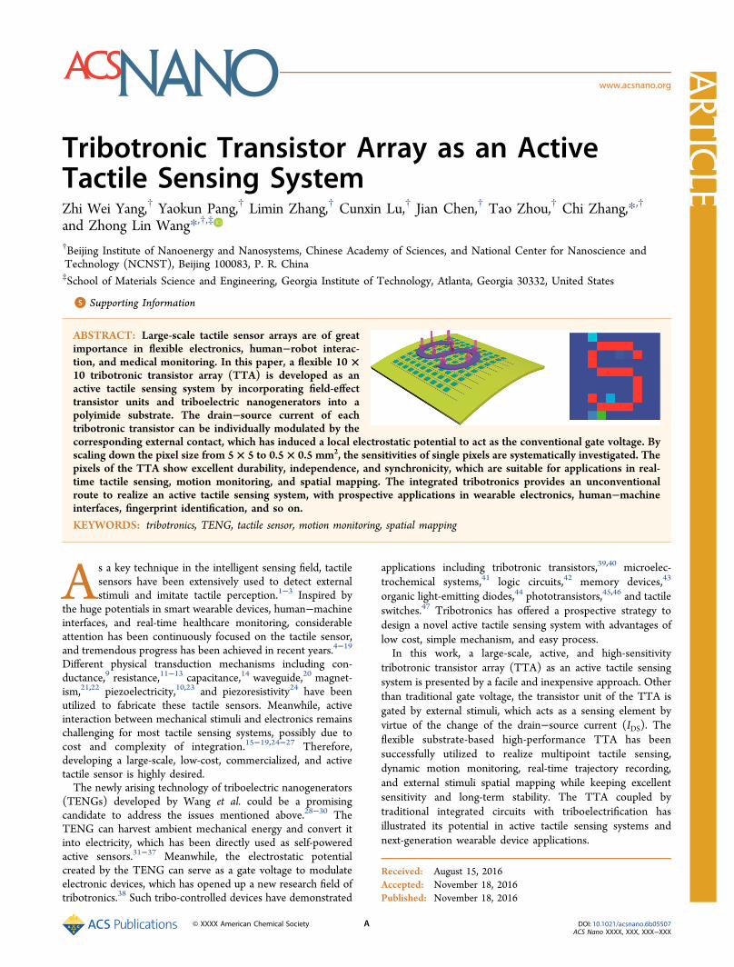
Tribotronic Transistor Array as an ActiveTactile Sensing SystemZhi Wei Yang,† Yaokun Pang,† Limin Zhang,† Cunxin Lu,† Jian Chen,† Tao Zhou,† Chi Zhang,*,†
and Zhong Lin Wang*,†,‡
†Beijing Institute of Nanoenergy and Nanosystems, Chinese Academy of Sciences, and National Center for Nanoscience andTechnology (NCNST), Beijing 100083, P. R. China‡School of Materials Science and Engineering, Georgia Institute of Technology, Atlanta, Georgia 30332, United States
*S Supporting Information
ABSTRACT: Large-scale tactile sensor arrays are of greatimportance in flexible electronics, human−robot interac-tion, and medical monitoring. In this paper, a flexible 10 ×10 tribotronic transistor array (TTA) is developed as anactive tactile sensing system by incorporating field-effecttransistor units and triboelectric nanogenerators into apolyimide substrate. The drain−source current of eachtribotronic transistor can be individually modulated by thecorresponding external contact, which has induced a local electrostatic potential to act as the conventional gate voltage. Byscaling down the pixel size from 5 × 5 to 0.5 × 0.5 mm2, the sensitivities of single pixels are systematically investigated. Thepixels of the TTA show excellent durability, independence, and synchronicity, which are suitable for applications in real-time tactile sensing, motion monitoring, and spatial mapping. The integrated tribotronics provides an unconventionalroute to realize an active tactile sensing system, with prospective applications in wearable electronics, human−machineinterfaces, fingerprint identification, and so on.
KEYWORDS: tribotronics, TENG, tactile sensor, motion monitoring, spatial mapping
As a key technique in the intelligent sensing field, tactilesensors have been extensively used to detect externalstimuli and imitate tactile perception.1−3 Inspired by
the huge potentials in smart wearable devices, human−machineinterfaces, and real-time healthcare monitoring, considerableattention has been continuously focused on the tactile sensor,and tremendous progress has been achieved in recent years.4−19
Different physical transduction mechanisms including con-ductance,9 resistance,11−13 capacitance,14 waveguide,20 magnet-ism,21,22 piezoelectricity,10,23 and piezoresistivity24 have beenutilized to fabricate these tactile sensors. Meanwhile, activeinteraction between mechanical stimuli and electronics remainschallenging for most tactile sensing systems, possibly due tocost and complexity of integration.15−19,24−27 Therefore,developing a large-scale, low-cost, commercialized, and activetactile sensor is highly desired.The newly arising technology of triboelectric nanogenerators
(TENGs) developed by Wang et al. could be a promisingcandidate to address the issues mentioned above.28−30 TheTENG can harvest ambient mechanical energy and convert itinto electricity, which has been directly used as self-poweredactive sensors.31−37 Meanwhile, the electrostatic potentialcreated by the TENG can serve as a gate voltage to modulateelectronic devices, which has opened up a new research field oftribotronics.38 Such tribo-controlled devices have demonstrated
applications including tribotronic transistors,39,40 microelec-trochemical systems,41 logic circuits,42 memory devices,43
organic light-emitting diodes,44 phototransistors,45,46 and tactileswitches.47 Tribotronics has offered a prospective strategy todesign a novel active tactile sensing system with advantages oflow cost, simple mechanism, and easy process.In this work, a large-scale, active, and high-sensitivity
tribotronic transistor array (TTA) as an active tactile sensingsystem is presented by a facile and inexpensive approach. Otherthan traditional gate voltage, the transistor unit of the TTA isgated by external stimuli, which acts as a sensing element byvirtue of the change of the drain−source current (IDS). Theflexible substrate-based high-performance TTA has beensuccessfully utilized to realize multipoint tactile sensing,dynamic motion monitoring, real-time trajectory recording,and external stimuli spatial mapping while keeping excellentsensitivity and long-term stability. The TTA coupled bytraditional integrated circuits with triboelectrification hasillustrated its potential in active tactile sensing systems andnext-generation wearable device applications.
Received: August 15, 2016Accepted: November 18, 2016Published: November 18, 2016
Artic
lewww.acsnano.org
© XXXX American Chemical Society A DOI: 10.1021/acsnano.6b05507ACS Nano XXXX, XXX, XXX−XXX

RESULTS AND DISCUSSION
Structure of the TTA. A schematic structure of the 10 × 10TTA is depicted in Figure 1a. Each pixel with a size of 5 × 5mm2, composed of a square Cu pad and a transistor unit, isintegrated on the top and bottom layer of a flexible polyimidesubstrate (the fabrication processes of TTA are described in
detail in the Methods). The gate electrode of the transistor iselectrically connected to the Cu pad by the via hole. The drainelectrodes of the 10 transistors in every column are commonlyconnected to an electrical wire, so are the source electrodes ofthose in every row. By selecting a column electrical wire, thecorresponding 10 pixels between this wire and the row
Figure 1. Structure of the TTA. (a) Schematic of a 10 × 10 TTA. Insets: Partial enlarged tilted views of the TTA configuration and pixelstructure, respectively. (b) Optical photograph of a fully integrated TTA with each sensing pixel of 5 × 5 mm2.
Figure 2. Schematic representations of the working principle for a single pixel and the equivalent circuit schematic of TTA. (a) Sketch of asingle pixel. (b−e) Change of the conduction channel width and resulting drain−source current (IDS) when the PTFE layer contacts with andseparates from the Cu pad. (f) Equivalent circuit schematic of the active tactile sensing system.
ACS Nano Article
DOI: 10.1021/acsnano.6b05507ACS Nano XXXX, XXX, XXX−XXX
B

electrical wires can be individually addressable. A photograph ofa well-designed TTA with good electrical contact is shown inFigure 1b with a resolution of 5 dpi.Principle of the TTA. Based on the coupling effects of the
transistor and contact electrification, the working principle ofthe TTA is demonstrated with cross-sectional and equivalentcircuit schematics in Figure 2. The transistor unit consists of ann-type transistor and a diode, in which the source electrode ofthe transistor is interconnected with the anode of the diode.This configuration ensures the current flows through thetransistor in only one direction. In the original state (Figure2a), a polytetrafluoroethylene (PTFE) film is prepared to serveas the mobile friction layer for contact electrification, which canapproach and separate from the Cu pad by an external force.Since the PTFE is triboelectrically more negative than Cu,when the PTFE film is forced to fully contact with the Cu pad,equal negative and positive charges can be induced on thesurfaces of the PTFE film and the Cu pad, respectively (Figure2b). At this moment, there is no conduction channel betweenthe source and drain electrode, hence generating little IDS.When the PTFE film is gradually separated from the Cu pad(Figure 2c), an electric field and a potential drop are createddue to the electrostatic induction and the edge electric fieldleakage from the finite size Cu pad and PTFE film, resulting ina built-in voltage at the gate electrode and generating aninversion conduction channel that enables electrons to flowfreely between the drain and source electrodes. Under thiscircumstance, the IDS can be produced with an applied drain−
source voltage (VDS). Further increase of the separationdistance is equivalent to enhancing the gate voltage (VGS),which can lead to the increase of the conduction channel widthand thus an evidently increased IDS. Predictably, once theseparation distance increases to a threshold (Figure 2d), thetriboelectric-charge-induced gate voltage and resulting currentwill remain stable at a maximum value if the PTFE filmcontinues to be moved vertically away from the Cu pad. Whenthe mobile PTFE film is pressed to approach the Cu pad again(Figure 2e), recovery of the IDS can be observed. In the wholeprocess, the IDS of the transistor is able to be tuned by theexternally physical access/contact, in place of the electricallyapplied gate voltage.As can be seen from the equivalent circuit diagram of the
TTA in Figure 2f, each pixel is addressed individually by acorresponding single-electrode TENG (SE-TENG). Comparedto sensor arrays with every pixel grounded or addressedindividually,2,9,14,32,34 a distinct advantage of a p × q TTA isthat the addressing lines have been greatly reduced from p × qto p + q. This reduction is also attributed to the addition of adiode in each pixel, which enables the unidirectional flow of IDSin the pixel without any interference of other pixels. In this case,the complex electrical connection of the TTA has beensignificantly simplified to 20 addressing lines, thus obviouslyenhancing the addressing speed and facilitating future develop-ment of a large-area TTA with simplified but effective electricalconnection.
Figure 3. Electrical characterization of single sensing pixel in TTA. (a) Sensitivity of the pixel, represented by an output current as a functionof separation distance. An ultrahigh sensitivity of 1.029 mm−1 is obtained below 3 mm and sharply declines to 0.0778 mm−1 in the range of 3−9 mm. Inset: Schematic illustration of the sensitivity test of the pixel. (b) Durability test for more than 700 contact−separation cycles,demonstrating the excellent performance of the sensing device with negligible current degradation. Inset: Comparison of currentcharacteristics of two enlarged areas. (c) Output current characteristics of two pixels in individual and simultaneous contact−separationprocess to demonstrate their independence and synchronicity characteristics. (d) Partial enlarged view of the current characteristic, showingthe gradual change trend of the IDS of a single pixel in the temporal domain and its color display.
ACS Nano Article
DOI: 10.1021/acsnano.6b05507ACS Nano XXXX, XXX, XXX−XXX
C

Characteristics of the Single Sensing Pixel in TTA. Toevaluate the sensing characteristics of the TTA, the distance-dependent performance of a single pixel was preciselydetermined by manual translation stages. The sensitivity ofthe TTA is defined as
= Δ ΔS I I d( / )/0 (1)
where ΔI is the relative change in the IDS, I0 is the initial currentof the pixel without external stimuli, and Δd is the distancechange between the PTFE film and the Cu pad. To quantify theparameter distance, the fully physical contact state between thePTFE film and the Cu pad was selected as the initial position.When the PTFE film was moved outward by an external force,the distance increased. Figure 3a shows the current response ofthe pixel to the distance, and the schematic illustration of thesensitivity test is shown in the inset. Initially, the pixel displayeda high sensitivity of 1.029 mm−1 even with a slight distanceincrease. However, once the PTFE film surpassed a “criticaldistance” of 3 mm, a remarkable sensitivity decrease of morethan an order of magnitude could be observed. As the distancecontinued to increase, the output current finally saturated andthe pixel would no longer be sensitive to the distance change.Once the PTFE film was forced to approach and ultimatelycontact with the Cu pad again, an inverse process would beseen. The whole process could be ascribed to the triboelectriccharge redistribution in the gate electrode of the pixel, whichhas been elaborated in its working mechanism presented inFigure 2.In order to comprehensively analyze the influence of the
separation distance on the triboelectric-charge-induced VGS andthe modulated IDS, a finite-element simulation was performedusing COMSOL to illustrate the potential distribution at thegate electrode of the tribotronic transistor (Figures S1 and S2).Besides this simulation, output and transfer characteristic curvesof a representative transistor were measured and depicted(Figure S3a shows the output characteristic of the transistor,and transfer curves in linear, log and root square scale areprovided in Figure S3b−d, respectively). Based on theestablished model that a PTFE film separated from andapproached a Cu pad, which was electrically connected to thegate electrode of a transistor, the exact same geometryparameters were utilized to obtain an accurate result. ThePTFE film (25 μm thick) had a size of 5 × 5 mm2, so did theCu pad (10 μm in thickness). The charge density was assumedto be −10 μC m−2 on the contacting surface of the PTFE filmand +10 μC m−2 on the surface of the Cu pad. The distancebetween the PTFE film and the Cu pad ranged from 0 to 12mm. One point that should be emphasized was that changes inthese assumed parameters aforementioned would only affectthe magnitude of the result and not the changing trend. Aftermaking these assumptions, electric potential distribution (d =0.2, 1, 2, 4, 6, 10, and 12 mm) at the gate electrode wassimulated and is presented in Figure S1. It indicated anincreasing trend of the VGS with the increase of the separationdistance. When d increased from 0 to 12 mm, thecorresponding VGS increased from 0 to 4.74 V. Besides thisresult, the relationship between the triboelectric-charge-inducedVGS and separation distance was also calculated and graphed inFigure S2. As the distance grew continually, the VGS exhibited aslower growth over 3 mm. This phenomenon could be verypersuasive because a similar trend was found in Figure 3a andFigures S2 and S3a. When the separation distance kept growing(or the VGS), a relative slow growth of the IDS could be clearly
observed. Convincingly, these results proved the relationshipbetween the separation distance and the IDS of the transistor.To sum up, the simulated analysis in Figures S1 and S2, alongwith the transfer and output curves in Figure S3, which was ingood agreement with the measured results in Figure 3a, furtherconfirmed the validity of employing the external force tosubstitute the electrical gate voltage and realize the modulationof IDS via the change of electrostatic potential.According to previous studies,34,48,49 the induced electro-
static potential has a close relation with the amount oftransferred charges. To better understand the influence of Cupad size in the sensitivity and acquire a possibly high resolutionof the TTA, the sensitivities of single pixel with different sizeswere systematically investigated. As shown in Figure S4, theIDS−distance curves of four pixels with corresponding Cu padarea varying from 4 × 4 to 0.5 × 0.5 mm2 were obtained, andthey provided a clear view of the pixel sensitivity changes.Three typical regions of sensitivity could be found in eachfigure, which was in good agreement with the result in Figure3a. The experimental results indicated that, as the pixel sizediminished, the corresponding sensitivity also declined both inhigh- and low-sensitivity regions. It was noteworthy that, inFigure S4d, the pixel with its size of 0.5 × 0.5 mm2 displayeddistinguishable sensitivities of 0.116 and 0.0085 mm−1
(according to the defined sensitivity in eq 1) in two differentregions even if the IDS was unable to decrease to zero when thePTFE film moved to fully contact the Cu pad. This result couldbe attributable to the diminished area of the contact Cu padand proportionately decreased electrostatic charges, as previousresearch has demonstrated. Due to the shrunken area of the Cupad, the edge electric leakage would be more distinct, whichleads to a higher proportion of triboelectric charges on the Cupad transferred to the gate electrode. Nevertheless, since thearea of the Cu pad was reduced more rapidly, in fact, theamount of the total charges transferred diminished. Meanwhile,the transistors used in all experiments were maintained thesame and had the same characteristics to be gated.Consequently, as the area of the Cu pad shrank, a poorersensing performance was observed in Figure S4a−d. In FigureS4d, the Cu pad size was 100 times smaller than that in Figure3a, causing the created electrostatic potential to be insufficientto shut down the conduction channel. Hence, the IDS couldremain above zero when the distance returned to the “fullyphysical contact state”. Due to this result, a square pixel with0.5 mm length size and good sensitivity was used as the smallestpixel in our research, realizing a resolution of about 50 dpi.Response time of the pixel is another essential sensing
feature of the TTA. In Figure S5a, the pixel exhibited a rapidresponse to the external stimuli during a quick contact−separation process. The measured response and recovery times,as illustrated in Figure S5b, were ∼78 and ∼86 ms, respectively,which should be sufficiently fast for practical applications.Moreover, a durability test was conducted at a constant VDS of2 V for more than 700 contact−separation cycles, asdemonstrated in Figure 3b. The output current showed noapparent signal shift or degradation during the test, proving theTTA can provide reproducible and reliable external tactileperception.Furthermore, to investigate whether pixels in the TTA can
function well individually and simultaneously, two pixels wereselected and electrical characteristics were determined, asplotted in Figure 3c. In the beginning, no PTFE film touchedthe two pixels, and they exhibited relatively stable, though
ACS Nano Article
DOI: 10.1021/acsnano.6b05507ACS Nano XXXX, XXX, XXX−XXX
D

slightly different, IDS. At nearly 3 s, a PTFE film slowlyapproached pixel 1, and the corresponding IDS of pixel 1showed a slow rate of decrease. From 5.5 s, decreasing thedistance to fully contact the Cu pad dramatically reduced thecurrent by more than 4 orders of magnitude to almost zero inless than 0.5 s, which could be supported in Figure 3a. In themeantime, pixel 2 presented a nearly unvaried IDS, proving thatit was not influenced and each pixel could work independently.Then, as the PTFE film touched both pixels, similar decreasingtrends of the IDS were obtained, which strongly supported thatpixels could work synchronously. It should also be mentionedin this experiment that, though there were variations in IDSamong different pixels, only the magnitude of IDS was affected,not the decreasing or increasing trend. Another factor thatshould be taken into account is that the output current signalinitially experienced a gradual change and then a fast trend ofdecrease, as depicted in the color display in Figure 3d. Thisphenomenon is of great importance because it exhibits that theIDS has a different responsive extent according to varyingdistance between the PTFE film and the Cu pad, signifying thatthe TTA can be constructed to resolve gradual changes inresponding to external access. Owing to the excellent sensingcapabilities, these sensing pixels are suitable for large-scaleintegration into a flexible substrate and have a widespread range
of applications, such as tactile sensing, e-skins, and healthcaremonitoring.
Application of the TTA for Active Tactile Sensing. Inorder to fulfill TTA’s potential in active tactile sensingapplications, these sensor pixels are integrated into a sensingdevice system, which provides a touch−user interface, enablingthe tactile profile, dynamic motion, and trajectory to be spatiallymapped. As an illustration, a flexible 7 × 7 TTA was fabricated.All output current signals were acquired via the multichanneldata acquisition system. Figure 4a is a schematic illustration oftwo-point contact, and Figure 4b shows the measured IDS in thefirst column pixels of the TTA. An evident current fall of pixelR4-C1 and pixel R5-C1 could be seen, while other pixelsmaintained their IDS unchanged. According to the measuredcurrent signals, a reconstructed intensity map of all pixels, withcolors representing the output current signal for each pixel, isdemonstrated in Figure 4c and the two contact pixels wereprecisely identified (a short video demonstrating the multipointsensing process is provided in Video S1, SupportingInformation). Besides multipoint identification, monitoringthe motion and recording the trajectory of moving objectsalso demonstrated the intriguing features of the TTA. As aPTFE film (5 × 5 mm2 area) moved along the last row andthen the diagonal of the TTA, the trajectory profile could beclearly recorded in real-time and plotted as a two-dimensional
Figure 4. TTA for multipoint tactile sensing and motion monitoring. (a) Schematic illustration of two-point contact. (b) Output currents ofpixels in the first column measured by multichannel measurement system. (c) Corresponding current signals plotted as two-dimensionalintensity map. (d) Schematic of a ball moving along different pixels. (e) Output currents of pixels in the moving trajectory of the ball. (f) Two-dimensional intensity map reconstructed from (e) with the measured current signals during the ball moving.
ACS Nano Article
DOI: 10.1021/acsnano.6b05507ACS Nano XXXX, XXX, XXX−XXX
E

intensity graph, shown in Figure 4f (a ball was used tosubstitute the PTFE film for demonstration in Figure 4d).Apparently, a motion path, first moving from pixel R7-C1 topixel R7-C7 and then from pixel R7-C7 to pixel R1-C1diagonally, was distinguished in the graph, which was in goodaccord with the current signal change of pixels depicted inFigure 4e (videos of the motion monitoring and trajectoryrecording experiment are provided in Video S2 and Video S3 inthe Supporting Information). Notably, two current falls wereobserved in the IDS response of pixel R7-C6 in Figure 4e, andthe second one could be explained by the turning of the movingball to the diagonal direction, which placed the ball close topixel R7-C6 again. Therefore, these experiments validate thatTTA has good practicability for multipoint sensing, dynamicmovement monitoring, and trajectory tracking because of itsrelatively high measurement precision and real-time tracingability.Additionally, the sensing ability of the active tactile sensing
system has been further accessed by placing letter-shaped slabsonto the sensing pixels of a flexible 10 × 10 TTA. Here, aspresented in Figure 5a, the PTFE films clinging to C-, A-, andS-shaped acrylic slabs were prepared. A layer of elastic spongewas sandwiched between the PTFE film and the acrylic slab toensure the uniform distribution of pressure over an areacorresponding to the predesigned PTFE slabs. Before placingthese “letters” on the sensing area, a background mapping hadbeen accomplished in advance to serve as a reference, shown inFigure S6a (VDS = 2 V). The IDS distribution map showed gooduniformity in electrical characteristics among all 100 pixels, with94% of the output current values in the narrow range of 0.105± 0.009 A. Obvious current variations found in pixels like pixelR10-C3 and pixel R10-C4 could mainly be the result ofdifferent amounts of induced charges on the Cu pad after theinitial contact with the PTFE film. For the purpose ofminimizing the interference of current variations among pixels,the ratio of ΔI to I0 was used to reconstruct the intensity image
(a two-dimensional intensity map of measured IDS in the shapeof letter “A” is provided in Figure S6b, SupportingInformation), and Figure 5b−d displays the reconstructionsof the “letter” image and clearly shows that pixels contacting theslabs experienced the greatest relative current changes, exceptfor some pixels such as pixel R3-C3 and pixel R7-C2 in Figure5c. This phenomenon could be caused by the uneven surface ofthe PTFE film, which resulted in pixels that failed to touch thefilm and hence was unable to induce enough electrostaticcharges to tune the IDS. To eliminate such defective pixels, theperformance of the TTA could be further improved byconstructing a micro/nanostructure on the surface of thePTFE film and optimizing the experimental process, such asensuring the smoothness of the PTFE film to realize physicallyfull contact with the Cu pad. Apart from pixels covered by theletter, some pixels next to the covered area were also affected toa different degree, which could be reasonably interpreted as theinfluence of potential distribution between the PTFE film andthe Cu pad on these adjoining pixels, like pixel R3-C7 in FigureS3b. Nevertheless, C-, A-, and S-shaped images could bedistinctly recognized, manifesting its bright prospects in real-time tactile sensing and image reconstruction. Moreover, thesensing array can be packaged by integrating the PTFE filminto the system. With this design (detailed integration processis introduced in Methods and Figure S7), the tactile sensors areable to produce stable output signals whatever the touchingobjects are, therefore enlarging its application range.
CONCLUSIONS
In summary, this work presents a flexible substrate-based TTAas a large-scale and active tactile sensing system. Utilizing theelectrostatic potential created by the triboelectrification, the IDSof each transistor unit can be modulated for sensing theexternal mechanical stimuli. Unlike the proposed sensor arraysbefore, with complicated and high-cost fabrication procedures,
Figure 5. TTA as a fully integrated system for tactile sensing and map reconstruction. (a) Photograph of a 10 × 10 TTA with three as-fabricated letter-shaped acrylic slabs placed on the surface of its sensing area. (b) Corresponding three-dimensional and two-dimensionalnormalized IDS intensity map of the A-shaped letter. (c,d) Normalized two-dimensional intensity profile of current signal for the shape of “C”and “S” reconstructed by the tactile sensing system.
ACS Nano Article
DOI: 10.1021/acsnano.6b05507ACS Nano XXXX, XXX, XXX−XXX
F

the flexible TTA combines traditional electronic devices withcheap but practical polymer films for contact electrification toachieve real-time high sensing and dynamic mapping. Byinvestigating in detail the electrical characteristics of pixels, wedemonstrated the TTA’s durability, independence, andsynchronicity. Moreover, the pixel can even be scaled downto the size of 0.5 × 0.5 mm2 while maintaining good sensitivityand thus realizing a high resolution of the TTA. Single- andmultiple-point touch map reconstruction, motion monitoring,and trajectory recording have been successfully accomplished,all of which verifies the outstanding performances of the TTA.Relying on the core concepts of tribotronics, in the future,more electronics and modules could be included to construct amultifunctional system that not only allows tactile sensing butalso enables many other intelligent and significant function-alities. It is anticipated that the TTA can unlock a door to abroad range of applications in wearable electronics, human−machine interfaces, and personalized health monitoring.
METHODSFabrication of the Flexible TTA. A polyimide (PI) substrate (100
μm in thickness) was first cleaned with deionized water, ethanol, andacetone and was then blown dry. The PI substrate was treated at 120°C for 30 min. Localized via holes were drilled on the PI substrate, andsubsequently, 10 μm thick Cu was deposited onto the selective area ofboth sides of the PI substrate to serve as electrical wires. Accordingly,10 Cu electrodes in rows and 10 Cu electrodes in columns with awidth of 250 μm were patterned on the top and bottom layer of the PIsubstrate, respectively. Later, a layer of Ni (3 μm) was electroplated onthe top layer of the substrate according to the designed circuitconfiguration to form pads with the size of 5 × 5 mm2, followed by thedeposition of Cu (0.25 μm) to the corresponding area of electricallyplated nickel. As a final step, chips of microfabricated n-type transistorsand diodes based on a standard silicon process were integrated ontothe as-fabricated PI substrate. All the gate electrodes of the transistorswere bonded to the defined Cu pad area through the via hole, whilethe 100 drain electrodes and source electrodes were bonded to thepatterned Cu wire electrodes. With such a design, each pixel isindependent of any other pixels. To integrate the mobile electrificationlayer into the as-fabricated device, the freestanding PTFE film was firstadhered to another flexible PI substrate, and then the Cu pad and thePTFE film were separated by spacers (3M 4-4100 adhesive). Afterthese spacers were placed, the whole device was sealed by adhesivetape.Electrical Characterization of the TTA. Drain−source currents
and sensing characteristics of single pixels were determined using adigital multimeter (Agilent 34411A), a DC power supply (RekRPS6003D-2), and manual translation stages (NFP-3462) underambient condition at room temperature. A source meter (2612B,Keithley) was used to characterize the transfer and output character-istics of the transistor. To test the durability of the TTA, a steppingmotor (XRV76) was used to supply a periodical reciprocating motionat speed of 20 mm/s. All of the 100 pixels in the TTA were addressedindividually by iteratively switching a 128 channel multiplexer matrix(PXI-2530, PXI-2630B, National Instrument). The output currentsignals from each pixel in the TTA were measured and averaged usinga 61/2-digit digital multimeter (PXI-4072, National Instrument), and aconstant bias (VDS) was provided by a programmable DC powersupply (PXI-4110, National Instrument). A homemade dataacquisition system was utilized to record and process the outputcurrent signals of the fabricated TTA in real time and then toreconstruct the two-dimensional intensity map of the TTA underdifferent external stimuli.
ASSOCIATED CONTENT*S Supporting InformationThe Supporting Information is available free of charge on theACS Publications website at DOI: 10.1021/acsnano.6b05507.
Figures S1−S7 (PDF)Video S1: tribotronic transistor array for multipointtactile sensing (AVI)Video S2: tribotronic transistor array for dynamic motionmonitoring (AVI)Video S3: tribotronic transistor array for real-timetrajectory recording (AVI)
AUTHOR INFORMATIONCorresponding Authors*E-mail: [email protected].*E-mail: [email protected] Lin Wang: 0000-0002-5530-0380NotesThe authors declare no competing financial interest.
ACKNOWLEDGMENTSThe authors thank the National Natural Science Foundation ofChina (Nos. 51475099 and 51432005), Beijing Natural ScienceFoundation (No. 4163077), the Youth Innovation PromotionAssociation, CAS, the “thousands talents” program for thepioneer researcher and his innovation team, China, andNational Key Research and Development Program of China(2016YFA0202704) for support.
REFERENCES(1) Mannsfeld, S. C. B.; Tee, B. C.-K.; Stoltenberg, R. M.; Chen, C.V. H.-H.; Barman, S.; Muir, B. V. O.; Sokolov, A. N.; Reese, C.; Bao, Z.Highly Sensitive Flexible Pressure Sensors with MicrostructuredRubber Dielectric Layers. Nat. Mater. 2010, 9, 859−864.(2) Wang, C.; Hwang, D.; Yu, Z.; Takei, K.; Park, J.; Chen, T.; Ma,B.; Javey, A. User-Interactive Electronic Skin for InstantaneousPressure Visualization. Nat. Mater. 2013, 12, 899−904.(3) Hammock, M. L.; Chortos, A.; Tee, B. C.-K.; Tok, J. B.-H.; Bao,Z. 25th Anniversary Article: the Evolution of Electronic Skin (E-Skin):A Brief History, Design Considerations, and Recent Progress. Adv.Mater. 2013, 25, 5997−6038.(4) Chortos, A.; Bao, Z. Skin-Inspired Electronic Devices. Mater.Today 2014, 17, 321−331.(5) Kaltenbrunner, M.; Sekitani, T.; Reeder, J.; Yokota, T.; Kuribara,K.; Tokuhara, T.; Drack, M.; SchwOdiauer, R.; Graz, I.; Bauer-Gogonea, S.; Bauer, S.; Someya, T. An Ultra-Lightweight Design forImperceptible Plastic Electronics. Nature 2013, 499, 458−463.(6) Kim, D.-H.; Lu, N.; Ma, R.; Kim, Y.-S.; Kim, R.-H.; Wang, S.; Wu,J.; Won, S. M.; Tao, H.; Islam, A.; Yu, K. J.; Kim, T.-I.; Chowdhury, R.;Ying, M.; Xu, L.; Li, M.; Chung, H.-J.; Keum, H.; McCormick, M.; Liu,P.; Zhang, Y.-W.; Omenetto, F. G.; Huang, Y.; Coleman, T.; Rogers, J.A. Epidermal Electronics. Science 2011, 333, 838−843.(7) Harada, S.; Kanao, K.; Yamamoto, Y.; Arie, T.; Akita, S.; Takei, K.Fully Printed Flexible Fingerprint-Like Three-Axis Tactile and SlipForce and Temperature Sensors for Artificial Skin. ACS Nano 2014, 8,12851−12857.(8) Viry, L.; Levi, A.; Totaro, M.; Mondini, A.; Mattoli, V.; Mazzolai,B.; Beccai, L. Flexible Three-Axial Force Sensor for Soft and HighlySensitive Artificial Touch. Adv. Mater. 2014, 26, 2659−2664.(9) Takei, K.; Takahashi, T.; Ho, J. C.; Ko, H.; Gillies, A. G.; Leu, P.W.; Fearing, R. S.; Javey, A. Nanowire Active-Matrix Circuitry for Low-Voltage Macroscale Artificial Skin. Nat. Mater. 2010, 9, 821−826.
ACS Nano Article
DOI: 10.1021/acsnano.6b05507ACS Nano XXXX, XXX, XXX−XXX
G

(10) Wu, W.; Wen, X.; Wang, Z. L. Taxel-Addressable Matrix ofVertical-Nanowire Piezotronic Transistors for Active and AdaptiveTactile Imaging. Science 2013, 340, 952−957.(11) Lee, S.; Reuveny, A.; Reeder, J.; Lee, S.; Jin, H.; Liu, Q.; Yokota,T.; Sekitani, T.; Isoyama, T.; Abe, Y.; Suo, Z.; Someya, T. ATransparent Bending-Insensitive Pressure Sensor. Nat. Nanotechnol.2016, 11, 472−478.(12) Chou, H.-H.; Nguyen, A.; Chortos, A.; To, J. W.F.; Lu, C.; Mei,J.; Kurosawa, T.; Bae, W.-G.; Tok, J. B.-H.; Bao, Z. A Chameleon-Inspired Stretchable Electronic Skin with Interactive Colour ChangingControlled by Tactile Sensing. Nat. Commun. 2015, 6, 8011.(13) Pan, L.; Chortos, A.; Yu, G.; Wang, Y.; Isaacson, S.; Allen, R.;Shi, Y.; Dauskardt, R.; Bao, Z. An Ultra-Sensitive Resistive PressureSensor Based on Hollow-Sphere Microstructure Induced Elasticity inConducting Polymer Film. Nat. Commun. 2014, 5, 3002.(14) Zang, Y.; Zhang, F.; Huang, D.; Gao, X.; Di, C.-A.; Zhu, D.Flexible Suspended Gate Organic Thin-Film Transistors for Ultra-Sensitive Pressure Detection. Nat. Commun. 2015, 6, 6269.(15) Sun, Q.; Kim, D. H.; Park, S. S.; Lee, N. Y.; Zhang, Y.; Lee, J. H.;Cho, K.; Cho, J. H. Transparent, Low-Power Pressure Sensor MatrixBased on Coplanar-Gate Graphene Transistors. Adv. Mater. 2014, 26,4735−4740.(16) Hong, S. Y.; Lee, Y. H.; Park, H.; Jin, S. W.; Jeong, Y. R.; Yun, J.;You, I.; Zi, G.; Ha, J. S. Stretchable Active Matrix Temperature SensorArray of Polyaniline Nanofibers for Electronic Skin. Adv. Mater. 2016,28, 930−935.(17) Ren, X.; Pei, K.; Peng, B.; Zhang, Z.; Wang, Z.; Wang, X.; Chan,P. K.L. A Low-Operating-Power and Flexible Active-Matrix Organic-Transistor Temperature-Sensor Array. Adv. Mater. 2016, 28, 4832−4838.(18) Schwartz, G.; Tee, B. C.-K.; Mei, J.; Appleton, A. L.; Kim, D. H.;Wang, H.; Bao, Z. Flexible Polymer Transistors with High PressureSensitivity for Application in Electronic Skin and Health Monitoring.Nat. Commun. 2013, 4, 1859.(19) Takahashi, T.; Takei, K.; Gillies, A. G.; Fearing, R. S.; Javey, A.Carbon Nanotube Active-Matrix Backplanes for Conformal Elec-tronics and Sensors. Nano Lett. 2011, 11, 5408−5413.(20) Yun, S.; Park, S.; Park, B.; Kim, Y.; Park, S. K.; Nam, S.; Kyung,K.-U. Polymer-Waveguide-Based Flexible Tactile Sensor Array forDynamic Response. Adv. Mater. 2014, 26, 4474−4480.(21) Zang, Y.; Zhang, F.; Huang, D.; Di, C.-A.; Zhu, D. SensitiveFlexible Magnetic Sensors Using Organic Transistors with Magnetic-Functionalized Suspended Gate Electrodes. Adv. Mater. 2015, 27,7979−7985.(22) Alfadhel, A.; Kosel, J. Magnetic Nanocomposite Cilia TactileSensor. Adv. Mater. 2015, 27, 7888−7892.(23) Sun, Q.; Seung, W.; Kim, B. J.; Seo, S.; Kim, S.-W.; Cho, J. H.Active Matrix Electronic Skin Strain Sensor Based on Piezopotential-Powered Graphene Transistors. Adv. Mater. 2015, 27, 3411−3417.(24) Park, J.; Lee, Y.; Hong, J.; Lee, Y.; Ha, M.; Jung, Y.; Lim, H.;Kim, S. Y.; Ko, H. Tactile-Direction-Sensitive and StretchableElectronic Skins Based on Human-Skin-Inspired Interlocked Micro-structures. ACS Nano 2014, 8, 12020−12029.(25) Harada, S.; Honda, W.; Arie, T.; Akita, S.; Takei, K. FullyPrinted, Highly Sensitive Multifunctional Artificial Electronic WhiskerArrays Integrated with Strain and Temperature Sensors. ACS Nano2014, 8, 3921−3927.(26) Gong, S.; Schwalb, W.; Wang, Y.; Chen, Y.; Tang, Y.; Si, J.;Shirinzadeh, B.; Cheng, W. A Wearable and Highly Sensitive PressureSensor with Ultrathin Gold Nanowires. Nat. Commun. 2014, 5, 3132.(27) Chen, L. Y.; Tee, B. C.-K.; Chortos, A. L.; Schwartz, G.; Tse, V.;Lipomi, D. J.; Wong, H.-S. P.; McConnell, M. V.; Bao, Z. ContinuousWireless Pressure Monitoring and Mapping with Ultra-Small PassiveSensors for Health Monitoring and Critical Care. Nat. Commun. 2014,5, 5028.(28) Fan, F. R.; Tian, Z.-Q.; Wang, Z. L. Flexible TriboelectricGenerator. Nano Energy 2012, 1, 328−334.(29) Zhang, C.; Tang, W.; Han, C. B.; Fan, F. R.; Wang, Z. L.Theoretical Comparison, Equivalent Transformation and Conjunction
Operations of Electromagnetic Induction Generator and TriboelectricNanogenerator for Harvesting Mechanical Energy. Adv. Mater. 2014,26, 3580−3591.(30) Fan, F.; Tang, W.; Yao, Y.; Luo, J.; Zhang, C.; Wang, Z. L.Complementary Power Output Characteristics of ElectromagneticGenerators and Triboelectric Generators. Nanotechnology 2014, 25,135402.(31) Tang, W.; Zhou, T.; Zhang, C.; Fan, F. R.; Han, C. B.; Wang, Z.L. A Power-Transformed-and-Managed Triboelectric Nanogeneratorand Its Applications in A Self-Powered Wireless Sensing Node.Nanotechnology 2014, 25, 225402.(32) Yang, Y.; Zhang, H.; Lin, Z.-H.; Zhou, Y. S.; Jing, Q.; Su, Y.;Yang, J.; Chen, J.; Hu, C.; Wang, Z. L. Human Skin BasedTriboelectric Nanogenerators for Harvesting Biomechanical Energyand as Self-Powered Active Tactile Sensor System. ACS Nano 2013, 7,9213−9222.(33) Li, X. H.; Han, C. B.; Jiang, T.; Zhang, C.; Wang, Z. L. A Ball-Bearing Structured Triboelectric Nanogenerator for NondestructiveDamage and Rotating Speed Measurement. Nanotechnology 2016, 27,085401.(34) Wang, X.; Zhang, H.; Dong, L.; Han, X.; Du, W.; Zhai, J.; Pan,C.; Wang, Z. L. Self-Powered High-Resolution and Pressure-SensitiveTriboelectric Sensor Matrix for Real-Time Tactile Mapping. Adv.Mater. 2016, 28, 2896−2903.(35) Han, C. B.; Zhang, C.; Li, X. H.; Zhang, L.; Zhou, T.; Hu, W.;Wang, Z. L. Self-Powered Velocity and Trajectory Tracking SensorArray Made of Planar Triboelectric Nanogenerator Pixels. Nano Energy2014, 9, 325−333.(36) Pang, Y. K.; Li, X. H.; Chen, M. X.; Han, C. B.; Zhang, C.;Wang, Z. L. Triboelectric Nanogenerators as A Self-Powered 3DAcceleration Sensor. ACS Appl. Mater. Interfaces 2015, 7, 19076−19082.(37) Zhang, L. M.; Xue, F.; Du, W.; Han, C. B.; Zhang, C.; Wang, Z.L. Transparent Paper-Based Triboelectric Nanogenerator as A PageMark and Anti-Theft Sensor. Nano Res. 2014, 7, 1215−1223.(38) Zhang, C.; Wang, Z. L. TribotronicsA New Field by CouplingTriboelectricity and Semiconductor. Nano Today 2016, 11, 521−536.(39) Zhang, C.; Tang, W.; Zhang, L.; Han, C.; Wang, Z. L. ContactElectrification Field-Effect Transistor. ACS Nano 2014, 8, 8702−8709.(40) Wu, J. M.; Lin, Y. H.; Yang, B. Z. Force-Pad Made fromContact-Electrification Poly (Ethylene Oxide)/InSb Field-EffectTransistor. Nano Energy 2016, 22, 468−474.(41) Zhang, C.; Tang, W.; Pang, Y.; Han, C.; Wang, Z. L. ActiveMicro-Actuators for Optical Modulation Based on A Planar SlidingTriboelectric Nanogenerator. Adv. Mater. 2015, 27, 719−726.(42) Zhang, C.; Zhang, L. M.; Tang, W.; Han, C. B.; Wang, Z. L.Tribotronic Logic Circuits and Basic Operations. Adv. Mater. 2015, 27,3533−3540.(43) Li, J.; Zhang, C.; Duan, L.; Zhang, L. M.; Wang, L. D.; Dong, G.F.; Wang, Z. L. Flexible Organic Tribotronic Transistor Memory for AVisible and Wearable Touch Monitoring System. Adv. Mater. 2016, 28,106−110.(44) Zhang, C.; Li, J.; Han, C. B.; Zhang, L. M.; Chen, X. Y.; Wang,L. D.; Dong, G. F.; Wang, Z. L. Organic Tribotronic Transistor forContact-Electrification-Gated Light-Emitting Diode. Adv. Funct. Mater.2015, 25, 5625−5632.(45) Pang, Y.; Xue, F.; Wang, L.; Chen, J.; Luo, J.; Jiang, T.; Zhang,C.; Wang, Z. L. Tribotronic Enhanced Photoresponsivity of A MoS2phototransistor. Adv. Sci. 2016, 3, 1500419.(46) Zhang, C.; Zhang, Z. H.; Yang, X.; Zhou, T.; Han, C. B.; Wang,Z. L. Tribotronic Phototransistor for Enhanced Photodetection andHybrid Energy Harvesting. Adv. Funct. Mater. 2016, 26, 2554−2560.(47) Xue, F.; Chen, L.; Wang, L.; Pang, Y.; Chen, J.; Zhang, C.;Wang, Z. L. MoS2 Tribotronic Transistor for Smart Tactile Switch.Adv. Funct. Mater. 2016, 26, 2104−2109.(48) Niu, S.; Liu, Y.; Wang, S.; Lin, L.; Zhou, Y. S.; Hu, Y.; Wang, Z.L. Theoretical Investigation and Structural Optimization of Single-Electrode Triboelectric Nanogenerators. Adv. Funct. Mater. 2014, 24,3332−3340.
ACS Nano Article
DOI: 10.1021/acsnano.6b05507ACS Nano XXXX, XXX, XXX−XXX
H

(49) Niu, S.; Wang, S.; Lin, L.; Liu, Y.; Zhou, Y. S.; Hu, Y.; Wang, Z.L. Theoretical Study of Contact-Mode Triboelectric Nanogeneratorsas an Effective Power Source. Energy Environ. Sci. 2013, 6, 3576−3583.
ACS Nano Article
DOI: 10.1021/acsnano.6b05507ACS Nano XXXX, XXX, XXX−XXX
I