transmissions electron microscopy (tem)€¦ · transmissions electron microscopy (tem) basic...
TRANSCRIPT

A.E. Gunnæs MENA3100 V18
Transmissions Electron Microscopy (TEM)
Basic principles
Diffraction
Imaging
Specimen preparation
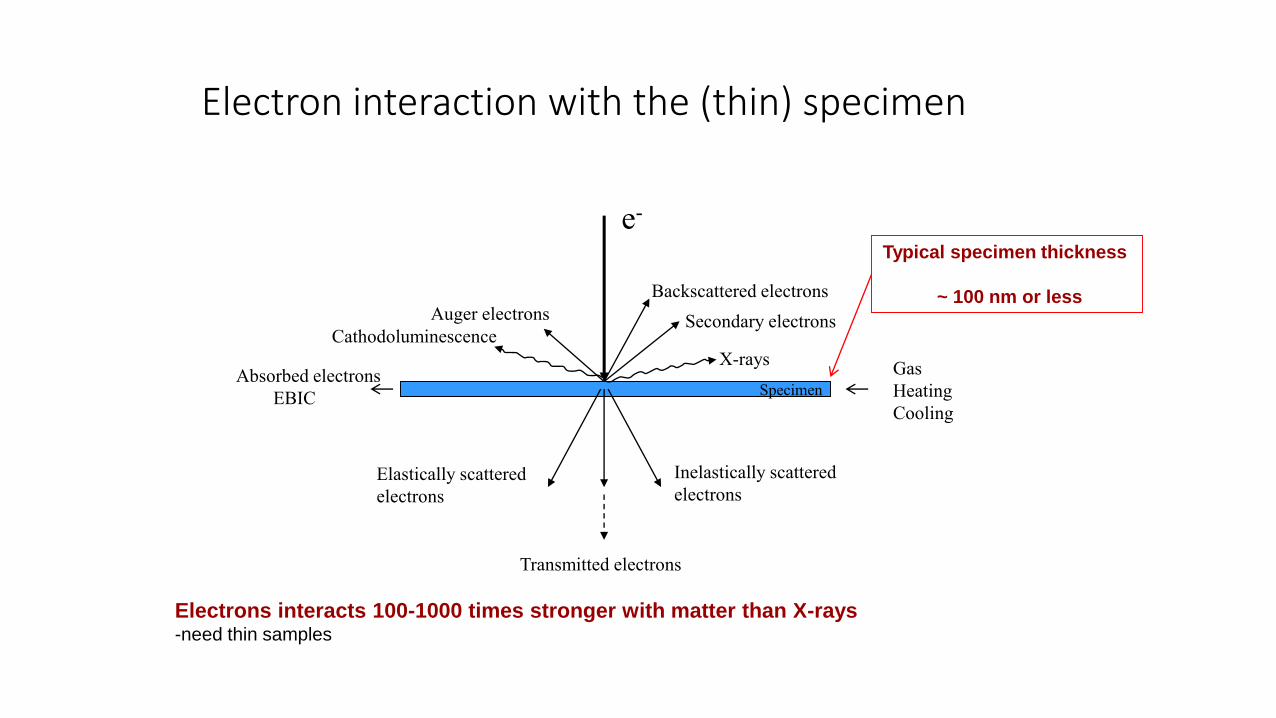
Electron interaction with the (thin) specimen
Specimen
e-
Transmitted electrons
Inelastically scattered
electrons
X-rays
Secondary electrons
Backscattered electrons
Auger electrons
Cathodoluminescence
Gas
Heating
Cooling
Absorbed electrons
EBIC
Elastically scattered
electrons
Typical specimen thickness
~ 100 nm or less
Electrons interacts 100-1000 times stronger with matter than X-rays-need thin samples

Operating modes
Convergent beam Parallel beam
Can be scanned
(STEM mode)
Specimen
Spectroscopy and mapping
(EDS and EELS)
Quartz (1mm)
AZO (sputtering, ~200 nm)
Cu2O (sputtering, 600nm)
TiO2 (ALD, 10 nm)
Example of EDS mapping in STEM mode.
EDS: Energy dispersive spectroscopy
EELS: Electron energy loss spectroscopy
STEM: Scanning transmission electron microscopy
HAADF: High angular annular dark field
S. Gorantla
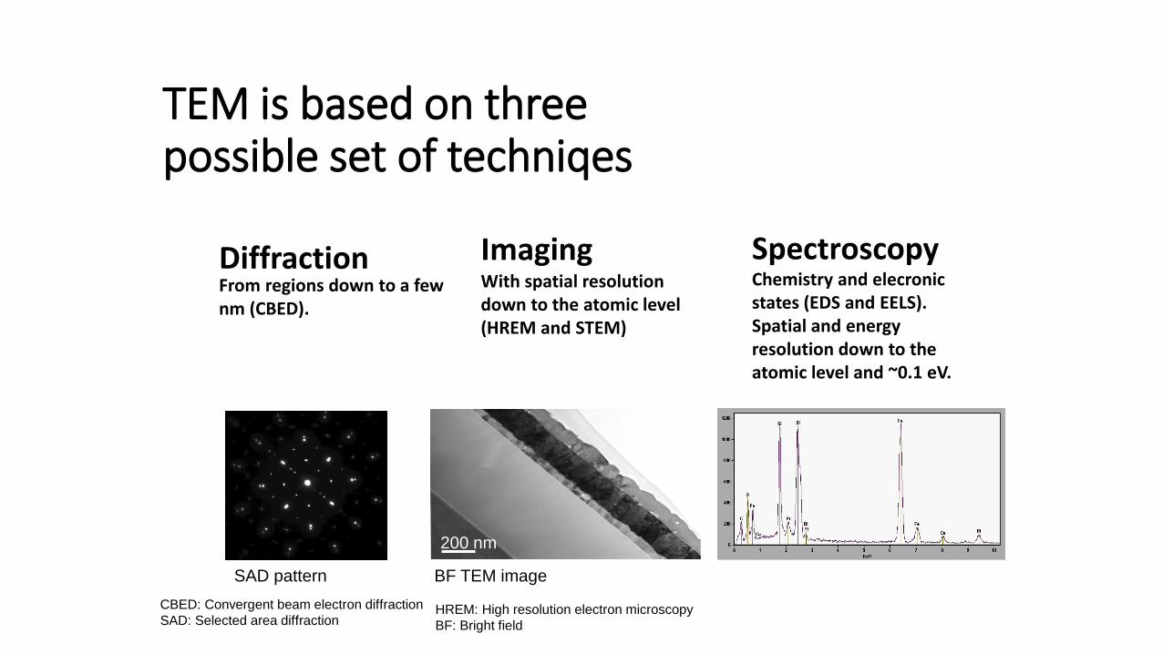
ImagingDiffraction SpectroscopyWith spatial resolution down to the atomic level (HREM and STEM)
Chemistry and elecronic states (EDS and EELS).Spatial and energy resolution down to the atomic level and ~0.1 eV.
From regions down to a few nm (CBED).
TEM is based on three possible set of techniqes
200 nm
HREM: High resolution electron microscopy
BF: Bright field
CBED: Convergent beam electron diffraction
SAD: Selected area diffraction
SAD pattern BF TEM image

Imaging and resolution
A.E. Gunnæs
Modern TEMs with Cs correctors have sub Å resolution!
Resolution of the eyes:~ 0.1-0.2 mm
Resolution in a visible light microscope: ~200 nm

Defects
Precipitates
Interfaces
Important for material properties
S. Gorantla
CuO
ZnO
HAADF image
Strain analysis around a dislocation core at the CuO-ZnO interface
Local atomic structure and composition,
Electronic structure and chemical bonding
The interesting objects for TEM is local structure and inhomogeneities in specimens

An example of a TEM study:
Identification of an unknown phase in a thin film
A.E. Gunnæs

Specimen: thin film of BiFeO3 + unknown phase
ab
c
BiBi
Fe
O O
Fe
Fe
Bi
O
Bi
Bi
O
Fe
O
O
Bi
O
Fe
Bi
Fe
O
Bi
O
Bi
O
Fe
O
Fe
O
Bi
Bi
O
Fe
O
Bi
Bi
O O
Bi
O
Fe
Fe
O
Fe
BiBi
PowderCell 2 .0
Goal to produce single phase:BiFeO3 with space grupe: R3C and celle dimentions: a= 5.588 Å c=13.867 Å
Metal organic compound on Pt
Heat treatment at 350oC (10 min) to
remove organic parts.
Process repeated three times before final
heat treatment at 500-700 oC (20 min) .
(intermetallic phase grown)
BF TEM image of the cross section of the specimen
200 nm
Si
SiO2
TiO2
Pt
BiFeO3
LimGlue
A.E. Gunnæs
50 nm
Tilting series around a dens row of
reflections in the reciprocal space
0o
19o
25o
40o
52o
Determination of the Bravais-lattice of an unknown crystalline phase
Courtesy: Dr. Jürgen Thomas, IFW-Dresden, Germany
Positions of the
reflections in the
reciprocal space
A. E. Gunnæs
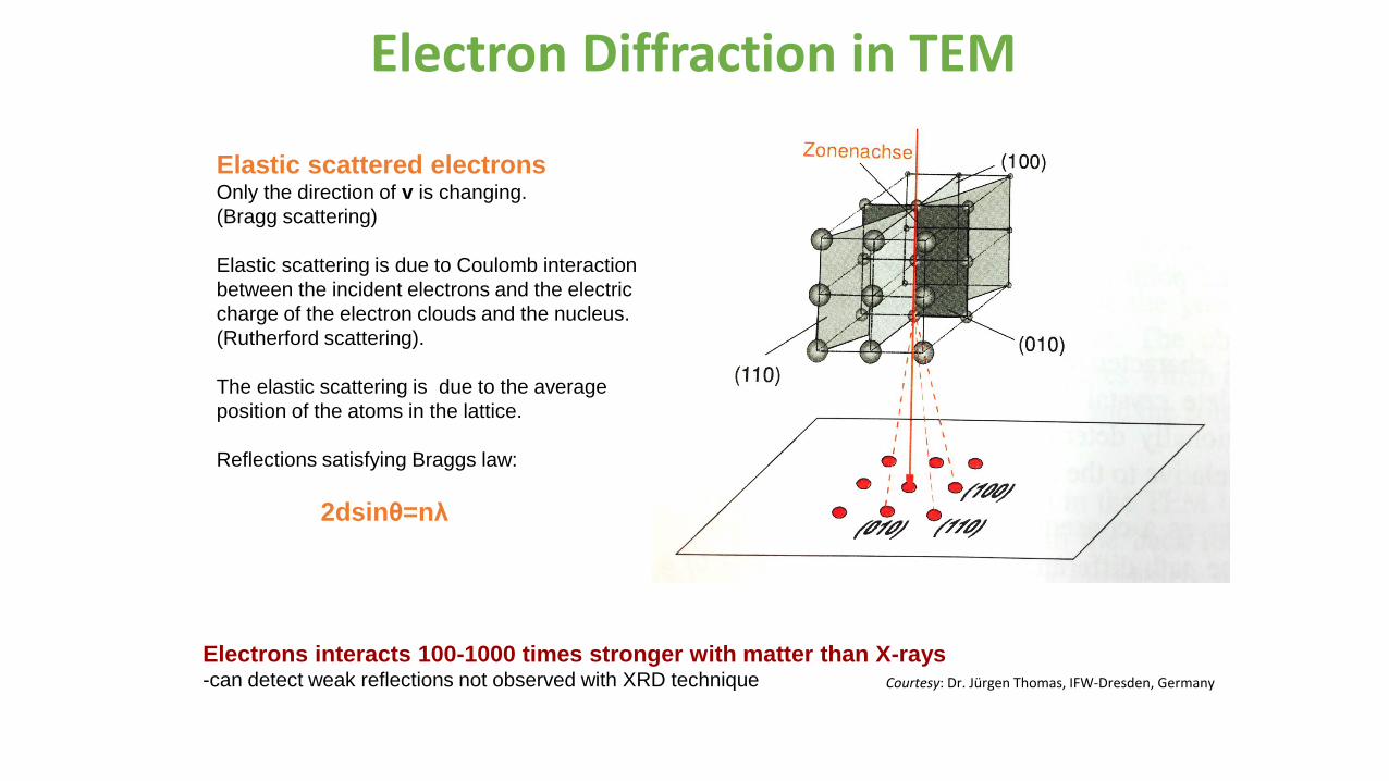
Elastic scattered electronsOnly the direction of v is changing.
(Bragg scattering)
Elastic scattering is due to Coulomb interaction
between the incident electrons and the electric
charge of the electron clouds and the nucleus.
(Rutherford scattering).
The elastic scattering is due to the average
position of the atoms in the lattice.
Reflections satisfying Braggs law:
2dsinθ=nλ
Electrons interacts 100-1000 times stronger with matter than X-rays-can detect weak reflections not observed with XRD technique
Electron Diffraction in TEM
Courtesy: Dr. Jürgen Thomas, IFW-Dresden, Germany

Bravais-lattice and cell parameters
From the tilt series we find that the unknown phase
has a primitive orthorhombic Bravias-lattice with
cell parameters:
a= 6,04 Å, b= 7.94 Å og c=8.66 Å
α= β= γ= 90o
6.0
4 Å
7.94 Å
a
bc
100
110
111
010
011
001101
[011] [100] [101]
d = L λ / R

Chemical analysis by use of EDS and EELS
Ukjent faseBiFeO3
BiFe2O5
1_1evprc.PICT
-0 200 400 600 800 10005
10
15
20
25
30
35
40
Energy Loss (eV)
CC
D c
ounts
x 1
000
Nr_2_1evprc.PICT
-0 200 400 600 800 1000
-0
2
4
6
8
10
12
14
Energy Loss (eV)
CC
D c
ounts
x 1
000
Ukjent faseBiFeO3
Fe - L2,3
O - K
500 eV forskyvning, 1 eV pr. kanal

Published structureA.G. Tutov og V.N. Markin
The x-ray structural analysis of the antiferromagnetic Bi2Fe4O9 and the isotypical combinations Bi2Ga4O9 and Bi2Al4O9
Izvestiya Akademii Nauk SSSR, Neorganicheskie Materialy (1970), 6, 2014-2017.
Romgruppe: Pbam nr. 55, celleparametre: 7,94 Å, 8,44 Å, 6.01Å
x y z
Bi 4g 0,176 0,175 0
Fe 4h 0,349 0,333 0,5
Fe 4f 0 0,5 0,244
O 4g 0,14 0,435 0
O 8i 0,385 0,207 0,242
O 4h 0,133 0,427 0,5
O 2b 0 0 0,5
ab
c
O
Bi
Fe
O
Fe
Bi
O
Fe O
O
O
Fe
Fe
OO
O
O
Fe
Bi
O
O
Bi
O
Bi
O
O
Bi
Fe
O
O
OO
Fe
Fe
O
O
O Fe
O
Bi
Fe
O
Fe
Bi
O
PowderCell 2 .0
Celle parameters found with electron diffraction (a= 6,04 Å, b= 7.94 Å and c=8.66 Å) fits reasonably well with the
previously published data for the Bi2Fe4O9 phase. The disagreement in the c-axis may be due to the fact that we
have been studying a thin film grown on a crystalline substrate and is not a bulk sample. The conditions for
reflections from the space group Pbam is in agreement with observations done with electron diffraction.
Conclusion: The unknown phase has been identified as Bi2Fe4O9 with space group Pbam with cell parameters
a= 6,04 Å, b= 7.94 Å and c=8.66 Å.

The construction of a TEM
A.E. Gunnæs
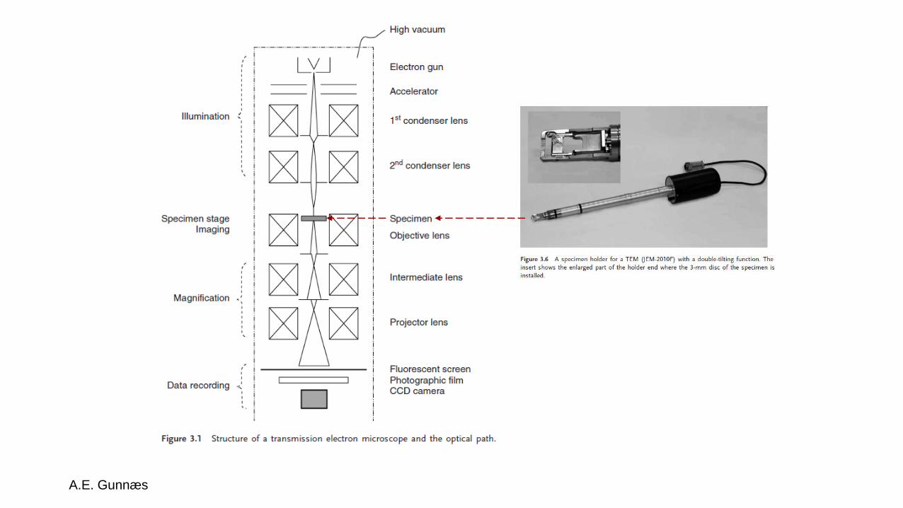
A.E. Gunnæs

Basic TEM
Electron gunApertures
Sample
holder
Fluorescence
screenRecording media
(Cameras, detectors)
Vacuum in the column
better than 10-6 Pa
Sample
1. and 2.
condenser lenses
Objective lens
Intermediate lenses
Projector lens
Similar components as a transmission light microscope

• Two types of emission guns:
• Thermionic emission
• W or LaB6
• Field emission
W ZrO/W
Cold FEG Schottky FEG
The electron source
Thermionic emission
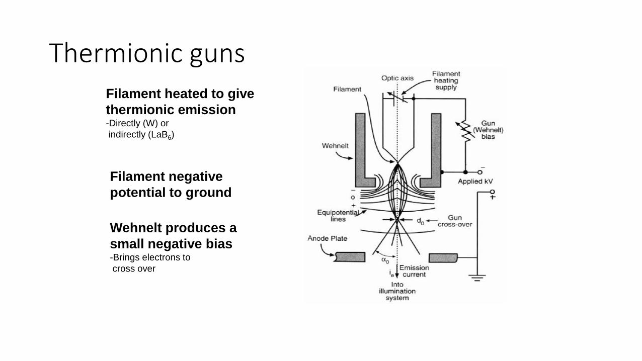
Thermionic gunsFilament heated to give
thermionic emission-Directly (W) or
indirectly (LaB6)
Filament negative
potential to ground
Wehnelt produces a
small negative bias-Brings electrons to
cross over

Field emission gun• The principle:
• The strength of an electric field E is
considerably increased at sharp points.
E=V/r
• rW < 0.1 µm, V=1 kV → E = 1010 V/m
• Lowers the work-function barrier so
that electrons can tunnel out of the tungsten.
• Surface has to be pristine (no contamination or oxide)
• Ultra high vacuum condition (Cold FEG) or poorer vacuum
if tip is heated (”thermal” FE; ZrO surface tratments → Schottky emitters).

Resolution
(JEOL2100F: 0.19 nm)
The point resolution in a TEM is limited by the aberrations of the lenses.-Spherical
- Chromatic
-Astigmatism

Electromagnetic lenses
F= -e(v x B)
A charged particle such as an electron, is deflected by a
magnetic field. The direction and magnitude of the force F,
on the electron is given by the vector equation:

Basic TEM
Electron gunApertures
Sample
holder
Fluorescence
screenRecording media
(Cameras, detectors)
Vacuum in the column
better than 10-6 Pa
Sample
1. and 2.
condenser lenses
Objective lens
Intermediate lenses
Projector lens
Similar components as a transmission light microscope

Simplified ray diagram
Objective lense
Diffraction plane (back focal plane)
Image plane
Sample
Parallel incoming electron beamSi
a
b
c
Po
wd
erCell 2
.0
1,1 nm
3,8
Å
Objective aperture
Selected area aperture
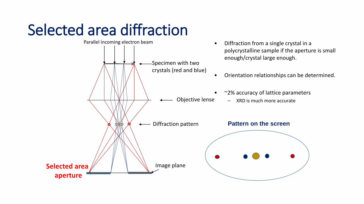
Selected area diffraction
Objective lense
Diffraction pattern
Image plane
Specimen with twocrystals (red and blue)
Parallel incoming electron beam
Selected area aperture
Pattern on the screen
• Diffraction from a single crystal in a polycrystalline sample if the aperture is small enough/crystal large enough.
• Orientation relationships can be determined.
• ~2% accuracy of lattice parameters
– XRD is much more accurate
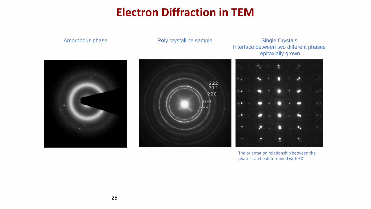
Poly crystalline sample
The orientation relationship between the phases can be determined with ED.
25
Single Crystals
Interface between two different phases
epitaxially grown
Electron Diffraction in TEM
Amorphous phase

Diffraction with large SAD aperture, ring and spot patterns
Similarities to XRD
SAD
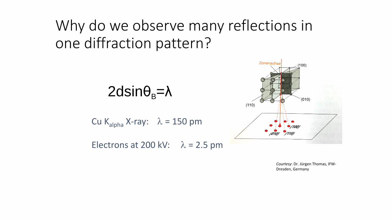
Why do we observe many reflections in one diffraction pattern?
Cu Kalpha X-ray: = 150 pm
Electrons at 200 kV: = 2.5 pm
2dsinθB=λ
Courtesy: Dr. Jürgen Thomas, IFW-Dresden, Germany

Cu Kalpha X-ray: = 150 pm => small k
Illustration with the Ewald Sphere The radius of the Ewald sphere is 1/ (=k)
Resiprocal lattice of a crystal
ko k
Electrons at 200 kV: = 2.5 pm => large k

ED and form effectsThe dimensions of the specimen affects the shape of the resiprocal lattice poins
Real space Resiprocal space

The intensity distribution around each reciprocal
lattice point is spread out in the form of spikes directed
normal to the specimen.2d sinθ = nλ
λ200kV = 0.00251 nm
Θ~1o
I(k’-k)I=(2/λ)sinθB=g

Zone axis and Laue zones
Zone axis [uvw]
(hkl)
uh+vk+wl= 0

Indexing diffraction patternsThe g vector to a reflection is normal to the
corresponding (h k l) plane and IgI=1/dnh nk nl
- Measure Ri and the angles between
the reflections
- Calculate di , i=1,2,3 (=K/Ri)
- Compare with tabulated/theoretical
calculated d-values of possible phases
- Compare Ri/Rj with tabulated values for
cubic structure.
- g1,hkl+ g2,hkl=g3,hkl (vector sum must be ok)
- Perpendicular vectors: gi ● gj = 0
- Zone axis: gi x gj =[HKL]z
- All indexed g must satisfy: g ● [HKL]z=0
(h2k2l2)
Orientations of corresponding
planes in the real space

TEM imaging with parallell incomming beam
A.E. Gunnæs
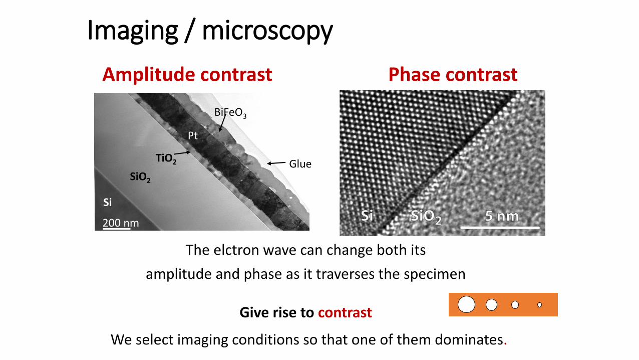
Imaging / microscopy
200 nm
Si
SiO2
TiO2
Pt
BiFeO3
Glue
Amplitude contrast Phase contrast
The elctron wave can change both its
amplitude and phase as it traverses the specimen
Give rise to contrast
We select imaging conditions so that one of them dominates.

Contrast• Difference in intensity of to adjacent areas:
11
12 )(
I
I
I
IIC
The eyes can not see intensity chanes that is less then 5-10%, however, contrast in images can be enhanced digitally.
NB! It is correct to talk about strong and week contrast but not bright and dark contrast

Use of apertures
Condenser aperture:Limits the number of electrons reaching the specimen (reducing the intensity),
Affecting the convergent of the electron beam.
Selected area aperture:Allows only electrons going through an area on the sample that is limited by the SAD aperture to
contribute to the diffraction pattern (SAD pattern).
Objective aperture:Allows certain reflections to contribute to the image. Increases the contrast in the image.
Bright field imaging (central beam, 000), Dark field imaging (one reflection, g), High resolution
Images (several reflections from a zone axis).

Simplified ray diagram
Objective lense
Diffraction plane(back focal plane)
Image plane
Sample
Parallel incoming electron beamSi
a
b
c
Po
wd
erCell 2
.0
1,1 nm
3,8
ÅObjective aperture
Selected area aperture

A.E. Gunnæs
Objective aperture: Contrast enhancement
No aperture used Central beam selected
Si Ag and Pb
glue(light elements)
hole
Amplitude contrast:
Mass-Density contrast and Diffraction contrast
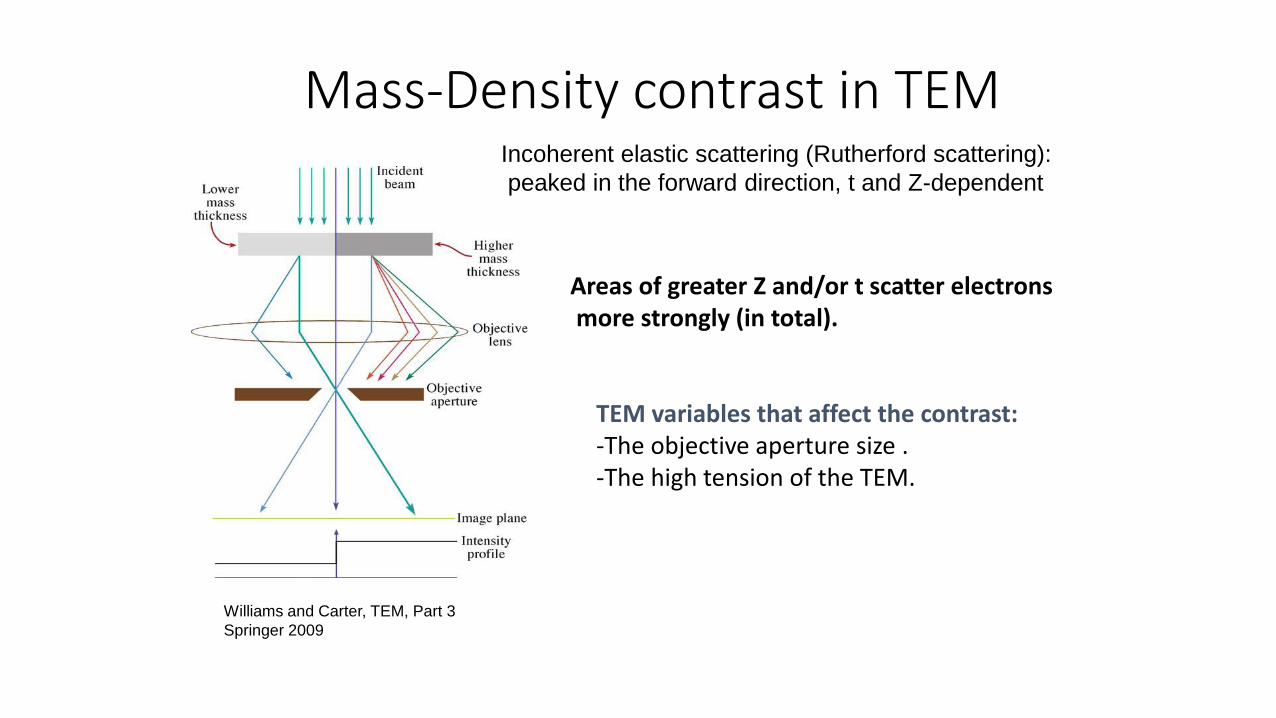
TEM variables that affect the contrast: -The objective aperture size .-The high tension of the TEM.
Areas of greater Z and/or t scatter electronsmore strongly (in total).
Mass-Density contrast in TEMIncoherent elastic scattering (Rutherford scattering):
peaked in the forward direction, t and Z-dependent
Williams and Carter, TEM, Part 3
Springer 2009

Mass-density contrast
A.E. Gunnæs

50 nm
Diffraction contrast
Objective aperture: Contrast enhancement
Intensity: Dependent on grain orientation
Try to make an illustration to explain why we get
this enhanced contrast when only the central beam
is selected by the optical aperture.

Diffraction contrast
A.E. Gunnæs
Bright field image

Size of objective apertureBright field (BF), dark field (DF) and High resolution EM (HREM)
BF image
Objectiveaperture
DF image
Amplitude/Diffraction contrast
HREM image
Phase contrast

Phase contrast: HREM and Moire’ fringes
http://www.mathematik.com/Moire/
A Moiré pattern is an interference pattern created, for example, when two grids are overlaid at an angle, or when they have slightly different mesh sizes (rotational and parallel Moire’ patterns).HREM image
Long-Wei Yin et al., Materials Letters, 52, p.187-191
Interference pattern

A.E. Gunnæs MENA3100 V18
Transmissions Electron Microscopy (TEM)
Basic principles
Diffraction
Imaging
Specimen preparation
PART II

Some repetiton….
A.E. Gunnæs
Specimen
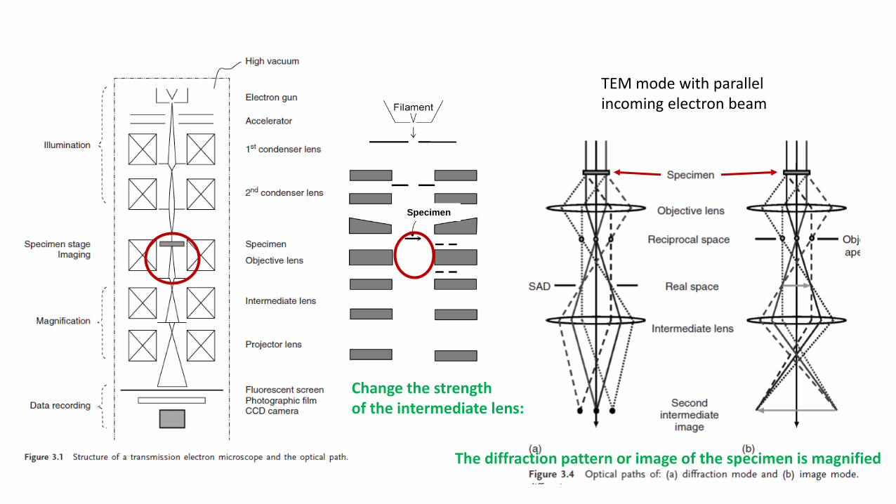
TEM mode with parallel incoming electron beam
Change the strength of the intermediate lens:
The diffraction pattern or image of the specimen is magnified
Specimen
TEM mode with parallel incoming electron beam
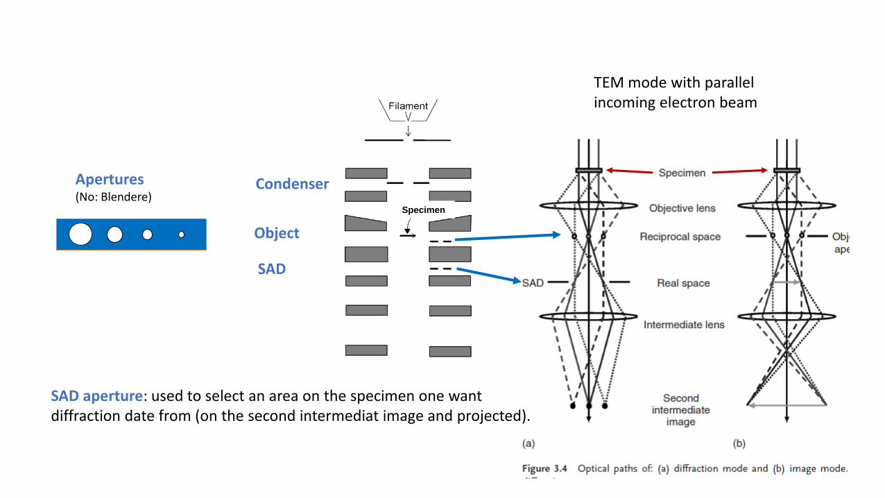
Apertures(No: Blendere)
Condenser
Object
SAD
SAD aperture: used to select an area on the specimen one wantdiffraction date from (on the second intermediat image and projected).
Specimen
TEM mode with parallel incoming electron beam
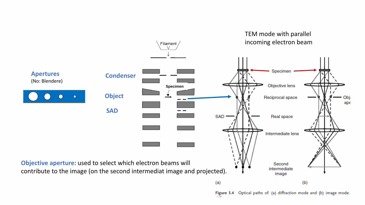
Apertures(No: Blendere)
Condenser
Object
SAD
Objective aperture: used to select which electron beams willcontribute to the image (on the second intermediat image and projected).

TEM mode with parallel incoming electron beam
Objective aperture: used to select which electron beams willcontribute to the image (on the second intermediat image and projected).
The objective aperture is used to controls the contrast in the image(enhances contrast).
One beam: Amplitude contrast (central (BF) or a scattered beam (DF))
Two or more beams: Phase contrast (+ amplitude)(HREM images (zone axis) or Moire)

Size of objective apertureBright field (BF), dark field (DF) and High resolution EM (HREM)
BF image
Objectiveaperture
DF image
Amplitude/Diffraction contrast
HREM image
Phase contrast

Phase contrast

Amplitude contrast
Diffraction contrast and Mass-density contrast
A TEM image will in most cases show both contrast types

TEM variables that affect the contrast: -The objective aperture size .-The high tension of the TEM.
Areas of greater Z and/or t scatter electronsmore strongly (in total).
Mass-Density contrast in TEMIncoherent elastic scattering (Rutherford scattering):
peaked in the forward direction, t and Z-dependent
Williams and Carter, TEM, Part 3
Springer 2009

Diffraction contrast in the TEM
A.E. Gunnæs
Bright field image
50 nm
The contrast is very sencitive to thespecimen orientation. (In contrast to mass-density contrast)

Effect of specimen tilt on diffraction contrast

Diffraction contrast
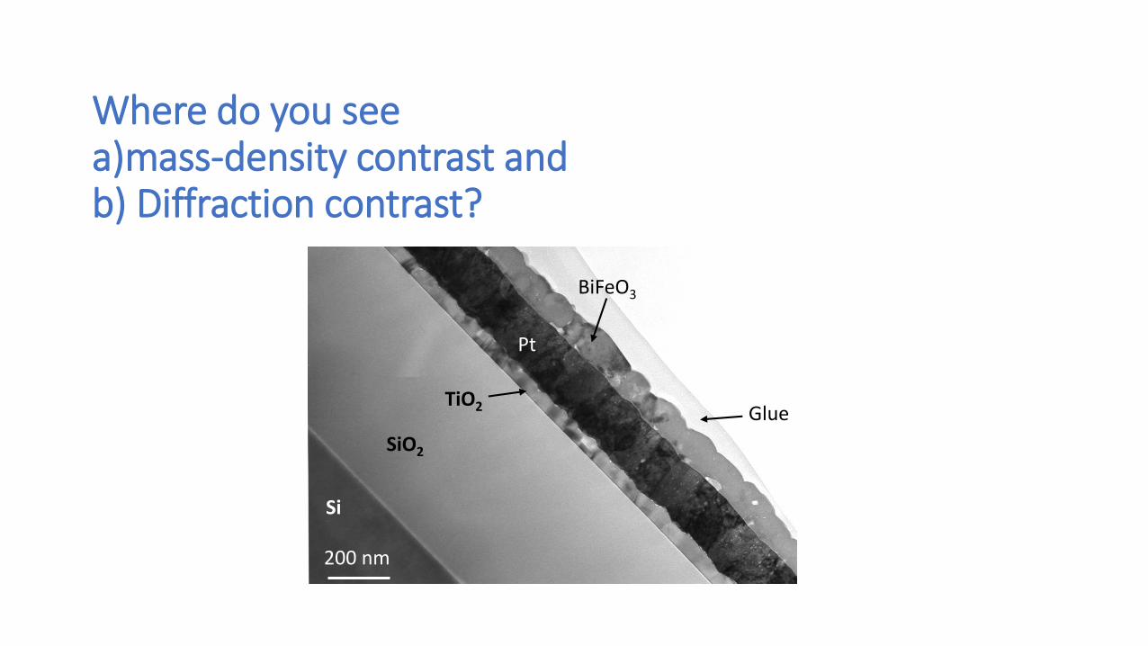
Where do you seea)mass-density contrast and b) Diffraction contrast?
200 nm
Si
SiO2
TiO2
Pt
BiFeO3
Glue

Crystal defects
- Effect of bending- Dislocations- Wedges

A.E. Gunnæs
BF image
DF image
DF image
Obj. aperture
Obj. lens
sample
Bending contours
Solberg, Jan Ketil & Hansen, Vidar (2001).
Innføring i transmisjon elektronmikroskopi

Bending contours

Dislocations

Double diffraction, extinction thickness
• Double electron diffraction leads to oscillations in the diffracted intensity with increasing thickness of the sample
• No double diffraction with XRD, kinematical intensities
• Forbidden reflection may be observed
• t0: Extinction thickness
• Periodicity of the oscillations
• t0=πVc/λIF(hkl)I
Incident beam
Diffracted beam Doublydiffracted beam
Transmitted beamWedge shaped TEM sample
t0

Simplified kinematical theory for perfect crystalsBasis of kinematical theory of electron diffraction for imperfect crystals:
Ψg(t)= ∫(πi/ξg) exp(-2πisgz)dz, Ψo=1, t: crystal thickess t
0
Intensity of the scattered beam g (dark field):
Ig= l Ψg(t) l2= sin2 πsgt/(ξgsg)
2
Intensity of the unscattered beam 0 (bright field):
I0= 1-Ig= 1- l Ψg(t) l2= 1 - sin2 πsgt/(ξgsg)
2
Ψg(t)= (i/ξgsg) exp(-πitsg) sinπsgt
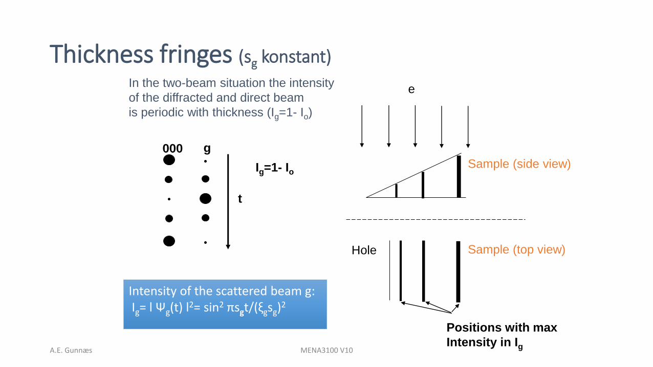
A.E. Gunnæs MENA3100 V10
Sample (side view)
e
000 g
t
Ig=1- Io
In the two-beam situation the intensity
of the diffracted and direct beam
is periodic with thickness (Ig=1- Io)
Sample (top view)Hole
Positions with max
Intensity in Ig
Thickness fringes (sg konstant)
Intensity of the scattered beam g: Ig= l Ψg(t) l
2= sin2 πsgt/(ξgsg)2

A.E. Gunnæs MENA3100 V10
Thickness fringes, bright and dark field images
Sample Sample
DF imageBF image

Kikuchi linesOrigin and use
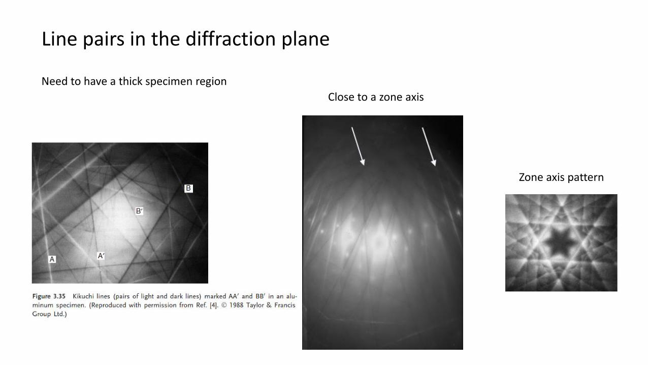
Line pairs in the diffraction plane
Zone axis pattern
Need to have a thick specimen region
Close to a zone axis

Need two scattering events
1. Inelastic2. Elastic
1.
-Angular distribution of inelastic scattered electrons falls of rapidly with angle. I=Iocos2α

Kikuchi pattern
http://www.doitpoms.ac.uk/index.html
http://www.doitpoms.ac.uk/tlplib/diffraction-patterns/kikuchi.php
ExcessDeficient
Excess
lineDeficient
line
2θB
θB
θB
Diffraction plane
Objective lens
1/d
.
1.Ineleastic scattering +
2. Bragg scattering event
What will happen if you tilt the specimen?
Incoherently and inelastically(ΔE~15-25 eV) scattered electrons give rise to diffuse background in the ED pattern

Kikuchi maps
http://www.umsl.edu/~fraundorfp/nanowrld/live3Dmodels/vmapframe.htm
000 g-g
Ig=I-g
Sg<0
Sg=0
Effect of tilting the specimen
Kossel cones
Parabolas
g and –g Kikuchi lines

TEM specimen preparation

What to considder before preparing a TEM specimen
• Ductile/fragile
• Bulk/surface/powder
• Insulating/conducting
• Heat resistant
• Single phase/multi phase
• Etc, etc…….
What is the objectiv of the TEM work?

Specimen preparation for TEM• Crushing
• Cutting• saw, “diamond” pen, ultrasonic drill,
ultramicrotomy
• Mechanical thinning• Grinding, dimpling,
• Tripod polishing
• Electrochemical thinning
• Ion milling
• Coating
• Replica methods
• FIB (Focused ion beam)
• Etc.

•Grids• Several types
• Different materials (Mo, Cu, Ni…)
• Support brittle materials
• Support small particles3 mm
The grid may contribute to the EDS signal.

Preparation of self-supporting discs Top view specimens
• Cutting• Ductile material or not?
• Grinding• 100-200 μm thick
• polish
• Cut the 3mm disc
• Dimple ?
• Final thinning• Ion beam milling
• Electropolishing

A.E. Gunnæs
Grind down/dimple
Cross section TEM sample preparation: Thin films
• Top view
• Cross section
or
Cut out a cylinderand glue it in a Cu-tube
Grind down andglue on support rings
Cut a slice of thecylinder and grindit down / dimple
Ione beam thinning
Cut out cylinder
Ione beam thinning
Cut out slices
Glue the interface of interest face to face together withsupport material
Cut off excessmaterial
• Focused Ion Beam (FIB)

Focused ion beam TEM specimen preparation