transistors - university of kentucky
TRANSCRIPT

TransistorsAll of our electronic technology is based on use of the transistor. They are used to amplify (increase the size of) analog signals and manipulate and store digital signals. Because most transistors are composed of semiconducting silicon, our present era has been called the “Silicon Age”.
This is a picture of the first transistor, invented by Shockley, Bardeen, and Brattain at Bell Labs in 1947.
Now a billion transistors can be packed (together with connecting wires, resistors, and capacitors, into a “Very Large Scale Integrated Circuit”, (VLSI) the size of a large coin. Most “Integrated Circuits” (IC’s) in consumer electronics are much smaller, with “only” tens to thousands of transistors.

Before discussing transistors, let’s discuss amplifiers in more general – these same considerations apply to older, vacuum tube amplifiers. An amplifier takes an input signal (a current or, more commonly, a voltage) and puts out a larger signal, which might even have more power (current times voltage). Since energy must be conserved, how is this possible?
Any amplifier, in addition to the input and output signals, must be connected to another power source, usually a DC-voltage supply. The amplifier takes energy from the source and turns it into energy in the output signal.

Usually, the signal we wish to amplify is one that is changing with time, e.g. an audio signal corresponding to a sound wave. To turn the various components in the amplifier circuit (e.g. transistors) on, dc-voltages must be provided (from the power supply). To separate the dc voltages from the input and output signal, capacitors can be used.
Recall from our February 28 lecture that when a capacitor is connected to a resistor, the voltage across it takes time (time =R*C) to change. Since the amplifier circuit will always contains resistance at its input and output connections, capacitors connected here will only pass high frequency signals with periods < RC and will block lower frequency (including DC) signals.
Such an amplifier can be used to increase the audio-frequency signal from a microphone (which turns a sound wave into an electrical signal) and to increase the audio-frequency signal to the speakers (which turn the electrical signal into a sound wave).

The name transistor comes from “trans-resistor” –it is a device that allows a voltage applied to one terminal to control the resistance between two other terminals. There are now many types of transistors that are useful for different applications, but one of the easiest to understand and most commonly used is an “n-channel MOSFET”, where MOSFET is an acronym for “Metal Oxide Semiconductor Field Effect Transistor”.
The figure shows a schematic of the transistor and the symbol for it in a circuit diagram. The gate is a metal film separated from the semiconducting channel by a thin insulator (typically silicon dioxide).

The n-channel MOSFET consists of two heavily doped n-type semiconductors (called the sourceand drain) on opposite ends of a very lightly doped p-type region, called the channel, as shown in the top figure. There is no electrical connection to the channel.
Because the channel is lightly doped and only has a few holes, the electrons which diffuse in from the source and drain completely fill these holes, so the channel is completely insulating. (In terms of our discussion of diodes, the depletion region extends completely through the channel.) This is shown in the lower figure.

Now apply a positive voltage to the metallic gate. The resulting electric field (going across the insulating oxide layer) will attract electrons from the source and drain into the channel, turning it into an effective n-type material. Now, since the source, channel, and drain are all n-type, there is a continuous conducting channel from the source to drain.
The resistance between the source and drain will depend (inversely) on how many electrons are pulled into the channel, so will depend on the magnitude of the gate voltage – we have made a resistor whose resistance value depends on the gate voltage.
[The MOSFET we described is technically known as an “enhancement-mode” device because the gate voltage increases the number of electrons in the channel. With different doping, one can make a “depletion-mode” device in which the gate voltage decreases the number of electrons.]
GS
D
G= gateS= sourceD = drain
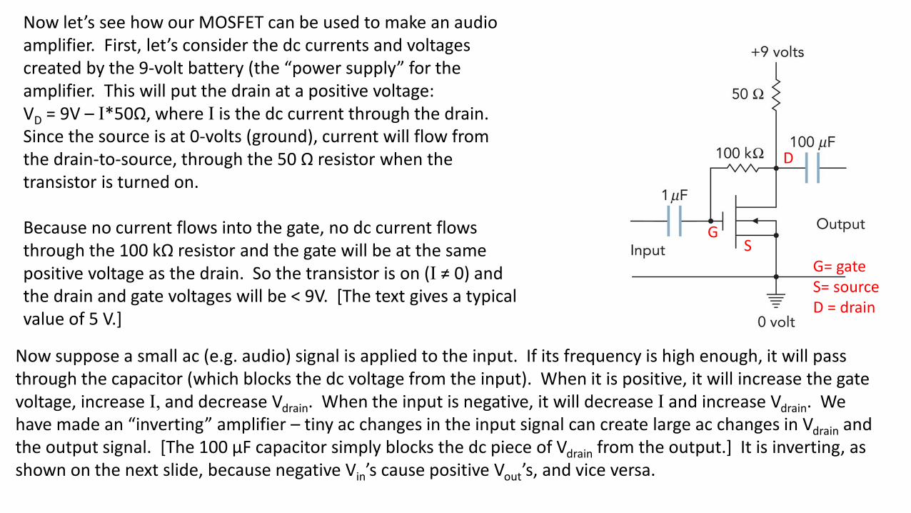
Now let’s see how our MOSFET can be used to make an audio amplifier. First, let’s consider the dc currents and voltages created by the 9-volt battery (the “power supply” for the amplifier. This will put the drain at a positive voltage: VD = 9V – I*50Ω, where I is the dc current through the drain. Since the source is at 0-volts (ground), current will flow from the drain-to-source, through the 50 Ω resistor when the transistor is turned on.
Because no current flows into the gate, no dc current flows through the 100 kΩ resistor and the gate will be at the same positive voltage as the drain. So the transistor is on (I ≠ 0) and the drain and gate voltages will be < 9V. [The text gives a typical value of 5 V.]
Now suppose a small ac (e.g. audio) signal is applied to the input. If its frequency is high enough, it will pass through the capacitor (which blocks the dc voltage from the input). When it is positive, it will increase the gate voltage, increase I, and decrease Vdrain. When the input is negative, it will decrease I and increase Vdrain. We have made an “inverting” amplifier – tiny ac changes in the input signal can create large ac changes in Vdrain and the output signal. [The 100 μF capacitor simply blocks the dc piece of Vdrain from the output.] It is inverting, as shown on the next slide, because negative Vin’s cause positive Vout’s, and vice versa.

Ft-1.5 -1.0 -0.5 0.0 0.5 1.0 1.5
sign
al
-10
-5
0
5
10
Vin
Vout
This shows input and output voltages for an inverting amplifier with “gain = 10”: the output is 10 x larger than the input. (The actual gain of our circuit will depend on the specific properties of the MOSFET.)
Note that the simple circuit we constructed will have “distortion: -- the output will not be exactly proportional to the input and the gain might be different at different frequencies. It also draws a lot of current (and power) from the 9-volt battery. These can all be corrected with more sophisticated circuits (with more components).

MOSFET’s can also be used in digital electronics to store and manipulate data. In this case, the transistor is used as an On/Off device (e.g. 1=on, 0 = off), where the input voltage for “on” is large enough to make the transistor very conducting.
For storage of digital information, two common techniques are used. For dynamic memory (in which case the data is lost when the instrument is turned off), the MOSFET charges or discharges a capacitor, which can be done relatively quickly. Slower, but used for memory even when the device is turned off, is flash memory in which the charge is stored on a second gate electrode inside the insulating layer of the MOSFET (called a floating gate because it does not have an electrical connection).
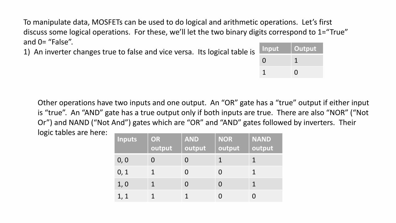
To manipulate data, MOSFETs can be used to do logical and arithmetic operations. Let’s first discuss some logical operations. For these, we’ll let the two binary digits correspond to 1=“True” and 0= “False”. 1) An inverter changes true to false and vice versa. Its logical table is Input Output
0 1
1 0
Other operations have two inputs and one output. An “OR” gate has a “true” output if either input is “true”. An “AND” gate has a true output only if both inputs are true. There are also “NOR” (“Not Or”) and NAND (“Not And”) gates which are “OR” and “AND” gates followed by inverters. Their logic tables are here:
Inputs OR output
AND output
NOR output
NAND output
0, 0 0 0 1 1
0, 1 1 0 0 1
1, 0 1 0 0 1
1, 1 1 1 0 0

For logic manipulations, one uses p-channel MOSFETs in addition to n-channel MOSFETs. In the p-channel device, one switches all the p and n regions of the n-channel device and also reverses the polarity of voltages. So it is turned on when a negative charge is applied to the gate and the conduction from the source through the channel to the drain is by holes. Now a positive charge corresponds to “1” or “true” and a negative charge corresponds to “0” or “false”.
The text describes how an inverter can be built from two transistors and a NAND-gate from four transistors. It turns out that these two logical elements can be combined to not only construct any logical operation but also any arithmetic operation, although in practice other logic elements are used to reduce size and increase speed.
[The earliest computers used vacuum tubes for logic elements.]
Of course, an audio signal is an analog signal, so the inputs and outputs of an audio recorder must be analog, even if the storage is digital. So an analog-to-digital (A-to-D) converter is needed at the input and a digital-to-analog (D-to-A) converter is needed at the output.

Finally, let’s discuss digital displays, e.g. for a computer, camera, cell phone, and television. For a black and white display, each pixel is either off (black) or on (white). Different shades of grey are created by the density of on-pixels in a small area. For a color display, there are 3 on/off dots (red, green, blue) in each pixel, and each dot can be turned on and off independently. Different colors are created by the densities in a small area of the colored dots that are turned on.
There are four common technologies used for displays:
1) LCD (Liquid Crystal Display) – this is the oldest. Light from a small bulb passes through a polarizer and a colored filter (e.g. sheet of a dye molecule) and then through a liquid crystal. This is a material with long-thin molecules that absorb light polarized along their long-direction. The logic signal voltage creates a small electric field that can rapidly turn the molecules so that that they are either parallel or perpendicular to the polarization direction of the light, thereby either absorbing or transmitting the light.
2) LED (Light Emitting Diode) – this is very similar to the LCD display, but it replaces the light sources behind the liquid crystals with LED’s, which require much less power than incandescent sources and are also smaller, so they can give thinner displays that don’t require as much cooling to keep running.
3) QLED (Quantum Light Emitting Diode) – this is similar to the LED display but uses “quantum dots” (nanoparticles with sizes comparable to visible wavelengths) instead of dye molecules as the color filter. These can actually act as colored amplifiers – blue light comes in from the LED which the quantum dot absorbs and then emits bright light at a longer wavelength (determined by the size of the dot).
4) OLED (Organic Light Emitting Diode) – this is the most different; it doesn’t use liquid crystals to absorb always on back-lights. Instead, it turns light-emitting diodes of different colors on and off for each pixel. It uses organic molecules as the semiconductor in the LED – different molecules can provide vivid light of the different colors. Because it is not back-lit, it brags that it has the “blackest “black”.

Exercises:35.The gate of a MOSFET is separated from the channel by a fantastically thin insulating layer. This layer
is easily punctured by static electricity, yet the manufacturers continue to use thin layers. Why wouldthickening the insulating layer spoil the MOSFET’s ability to respond to charge on its gate?
36.In an n-channel MOSFET, the source and drain are connected by a thin strip of p-type semiconductor.Why is this device labeled as having an n-channel rather than a p-channel?
37.A MOSFET doesn’t change instantly from a perfect insulator to a perfect conductor as you vary thecharge on its gate. With intermediate amounts of charge on its gate, the MOSFET acts as a resistor witha moderate electrical resistance. This flexibility allows the MOSFET to control the amount of currentflowing in a circuit. Explain why a MOSFET becomes warm as it controls that current.
38.The tiny MOSFETs that are used to move charge onto and off the capacitors in dynamic memory are sosmall that they’re never very good conductors. Why do their modest electrical resistances lengthen thetime it takes to store or retrieve charge from the memory capacitors?
40.If you connect the output of one inverter to the input of a second inverter, how will the output of thesecond inverter be related to the input of the first inverter?
41.Suppose you connected a microphone directly to a large unamplified speaker. Why wouldn’t the speakerreproduce your voice loudly when you talked into the microphone?
42.Why can’t an audio amplifier operate without batteries or a power supply?