transistors - a primerphys533/notes/week08_lectures.pdf · transistors - a primer ... • ac...
TRANSCRIPT
1
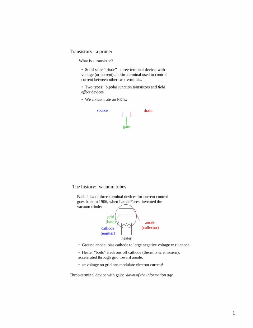
Transistors - a primer
What is a transistor?
• Solid-state “triode” - three-terminal device, with voltage (or current) at third terminal used to control current between other two terminals.
• Two types: bipolar junction transistors and field effect devices.
• We concentrate on FETs:
source drain
gate
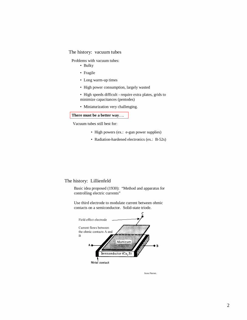
The history: vacuum tubes
Basic idea of three-terminal devices for current control goes back to 1906, when Lee deForest invented the vacuum triode:
cathode(emitter)
grid(base) anode
(collector)
heater
• Ground anode; bias cathode to large negative voltage w.r.t anode.
• Heater “boils” electrons off cathode (thermionic emission); accelerated through grid toward anode.
• ac voltage on grid can modulate electron current!
Three-terminal device with gain: dawn of the information age.
2
The history: vacuum tubes
Problems with vacuum tubes:• Bulky
• Fragile
• Long warm-up times
• High power consumption, largely wasted
• High speeds difficult - require extra plates, grids to minimize capacitances (pentodes)
• Miniaturization very challenging.
Vacuum tubes still best for:
• High powers (ex.: e-gun power supplies)
• Radiation-hardened electronics (ex.: B-52s)
There must be a better way….
The history: Lillienfeld
Basic idea proposed (1930): “Method and apparatus for controlling electric currents”
Use third electrode to modulate current between ohmic contacts on a semiconductor. Solid-state triode.
from Pierret.
3
Basic field effect transistor idea
Shockley (grid-like)
Lilienfeld
Gateacts like capacitor plate -applied voltage creates “channel” with free carriers, connecting sourceand drain.
Normally off:
Gateacts like grid - applied voltage restricts flow of (lightly doped) carriers from sourceto drain.
Normally on:
Why did these ideas first run into trouble? Surface states!Materials quality prevented practical FETs until 1955….
Types of field effect transistors
JFET MESFETJunction FET MEtal Semiconductor FET
• Channel, source, drain all same type of doped semiconductor.
• Normally “on” - requires gate voltage to turn off SD conduction; devices operate in depletion mode.
• Gate can be anywhere between source and drain.
• Current flow restricted by depletion zone (from pn junction in JFET; from Schottky barrier in MESFET).
• Fairly robust (no super-thin insulating layers, etc.)
different metals

4
Types of field effect transistors
MOSFET or MISFET
Metal Oxide or Metal Insulator Semiconductor FET
• Source, drain different doping type than bulk of semiconductor
• Normally OFF - gate must be biased sufficiently to invert channel region in order to see transistor action; devices operate in accumulation mode.
• Requires gate to extend over source and drain.
• Thin insulating barrier (gate oxide) necessary.
• Bulk may be p or n - complementary metal-oxide-semiconductor processing (CMOS).
channel
Types of field effect transistors
HEMT
High Electron Mobility Transistor
++++++++++++++++++++++++++++
undoped GaAs
• Source, drain are ohmic contacts to GaAs 2deg channel.
• Normally ON device (modulation doping) operates in depletion mode.
• Very high mobilities can lead to very high speed devices (cell phone electronics).
• Gate can be anywhere between source and drain.

5
Transistor operation and transconductance
One obvious figure of merit for a transistor is transconductance:
Basic transistor operation:
VG
loadID
G
Dm V
Ig
∂∂≡
Transistors with a higher gm are better switches than those with lower values.
The MOS system
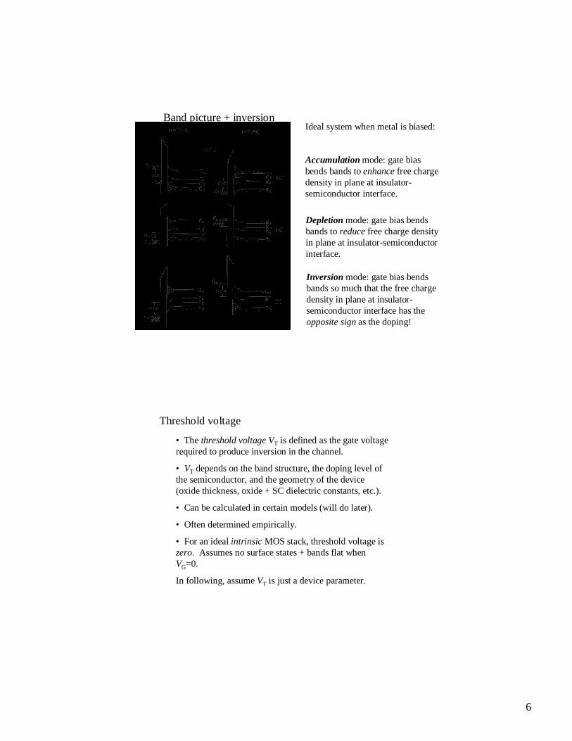
At left are band diagrams for metal-insulator-semiconductor stacks.
These are drawn assuming flat bands; that is, negligible charge transfer at interfaces to cause band bending, + negligible surface states.
For these ideal cases, with no bias on the metal, the charge density of the semiconductor = the full doped density right up to the interface.
n-type
p-type
n-type
p-type
6
Band picture + inversionIdeal system when metal is biased:
Accumulation mode: gate bias bends bands to enhance free charge density in plane at insulator-semiconductor interface.
Depletion mode: gate bias bends bands to reduce free charge density in plane at insulator-semiconductor interface.
Inversion mode: gate bias bends bands so much that the free charge density in plane at insulator-semiconductor interface has the opposite sign as the doping!
Threshold voltage
• The threshold voltage VT is defined as the gate voltage required to produce inversion in the channel.
• VT depends on the band structure, the doping level of the semiconductor, and the geometry of the device (oxide thickness, oxide + SC dielectric constants, etc.).
• Can be calculated in certain models (will do later).
• Often determined empirically.
• For an ideal intrinsic MOS stack, threshold voltage is zero. Assumes no surface states + bands flat when VG=0.
In following, assume VT is just a device parameter.
7
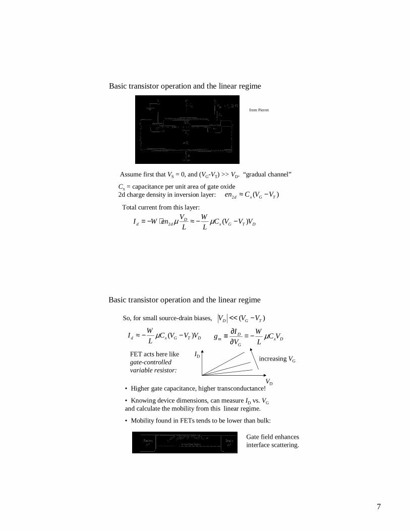
Basic transistor operation and the linear regime
from Pierret
Assume first that VS = 0, and (VG-VT) >> VD. “gradual channel”
Cx = capacitance per unit area of gate oxide2d charge density in inversion layer: )(2 TGxd VVCen −≈
Total current from this layer:
DTGxD
dd VVVCL
W
L
VenWI )(2 −−≈⋅−= µµ
Basic transistor operation and the linear regime
DTGxd VVVCL
WI )( −−≈ µ
)( TGD VVV −<<So, for small source-drain biases,
FET acts here like gate-controlled variable resistor:
DxG
Dm VC
L
W
V
Ig µ−=
∂∂≡
• Higher gate capacitance, higher transconductance!
• Knowing device dimensions, can measure ID vs. VG
and calculate the mobility from this linear regime.
• Mobility found in FETs tends to be lower than bulk:
VD
ID increasing VG
Gate field enhances interface scattering.
8
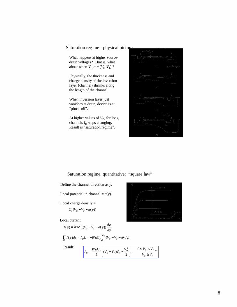
Saturation regime - physical picture
What happens at higher source-drain voltages? That is, what about when VD > ~ (VG-VT) ?
Physically, the thickness and charge density of the inversion layer (channel) shrinks along the length of the channel.
When inversion layer just vanishes at drain, device is at “pinch-off”.
At higher values of VD, for long channels ID stops changing. Result is “saturation regime”.
from Pierret
Saturation regime, quantitative: “square law”
Define the channel direction as y.
Local potential in channel = φ(y)
Local charge density =
))(( yVVC TGx φ−−
Local current: ∫∫ −−−== DV
TGx
L
D dVVCWLIdyyI00
)()( φφµ
dy
dyVVCWyI TGx
φφµ ))(()( −−=
Result:
TG
satDDDDTG
xD VV
VVVVVV
L
CWI
≥≤≤ −−= ,
2 0 ,
2)(
µ
9
“Square law”
TG
satDDDDTG
xD VV
VVVVVV
L
CWI
≥≤≤ −−= ,
2 0 ,
2)(
µ
Since ID only increases until pinch-off, can use above formula to find both pinch-off voltage and saturation current:
TGsatD VVV −=,2
, )(2 TG
xsatD VV
L
CWI −= µ
So, assuming constant mobility and ignoring changes in depletionwidth down length of channel, we find that saturation current scales quadratically with (VG-VT).
This provides another way of inferring mobility….
(Tacit assumption: source, drain contact resistances are negligible.)
What sets equilibrium depletion width?
First, recall some definitions:
Ei = energy of the middle of the gap in the semiconductor.
φS = potential at sc-oxide interface.
φF = bulk (E--EF)/e
φ(x) = (1/e)[Ei(bulk)-Ei(x)
ni = intrinsic carrier density = )2/exp( TkENN BgVC −

10
What sets equilibrium depletion width?
For nondegenerate semiconductors, −=
)/ln(
)/ln(
iDB
iAB
F
nNe
Tk
nNe
Tk
φ
Middle of depletion: FS φφ =
Onset of inversion: FS φφ 2=
Delta depletion
Exact self-consistent solution shows inversion charge confined to very thin layer at interface.
Depletion width increases only slightly once inversion occurs.
Approximation: further gating only affects inversion charge.
Depletion width at some surface potential:
2/1
02 = SA
s
eNd φεε
Depletion width at inversion:2/1
0 22 = F
A
sT eN
d φεε
11
“Bulk charge” picture
Takes into account variation in depletion width along channel.
Suppose the depletion width near source and drain under no bias is dT, and under bias it depends locally on position, d(y).
The induced charge density at position y is then
])([)( TATGx dydqNVVC −+−−− φ
inversion layer “free” charge additional exposed acceptors
Definingx
TAd C
deNV ≡
and substituting our delta-depletion results for the ds gives −+−−−− 12
1F
WTGx VVVCφφφ
“Bulk charge” picture
With this more careful accounting, we find a more exact expression for the ID-VD characteristics as a function of gate voltage:
TG
satDD
F
D
F
DFd
DDTG
xD VV
VVVVV
VVVV
L
CWI
≥≤≤ +− +−−−= ,
2/32 0 ,
4
31
21
3
4
2)(
φφφµ
Neither the bulk charge picture nor the square law picture predict saturation - it has to be inserted by hand into the model.
Complete numerical solution of the whole system does, of course, give pretty nice results, including saturation.
12
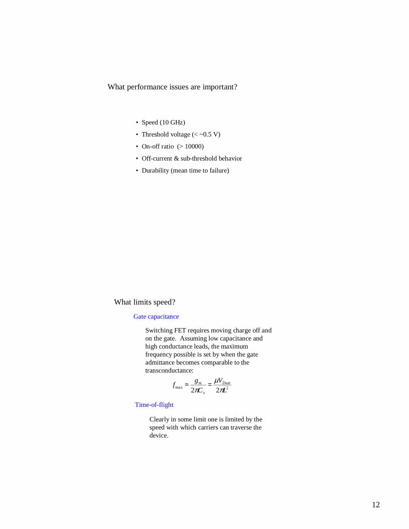
What performance issues are important?
• Speed (10 GHz)
• Threshold voltage (< ~0.5 V)
• On-off ratio (> 10000)
• Off-current & sub-threshold behavior
• Durability (mean time to failure)
What limits speed?
Gate capacitance
Switching FET requires moving charge off and on the gate. Assuming low capacitance and high conductance leads, the maximum frequency possible is set by when the gate admittance becomes comparable to the transconductance:
2max 22 L
V
C
gf Dsat
x
m
πµ
π=≈
Time-of-flight
Clearly in some limit one is limited by the speed with which carriers can traverse the device.
13
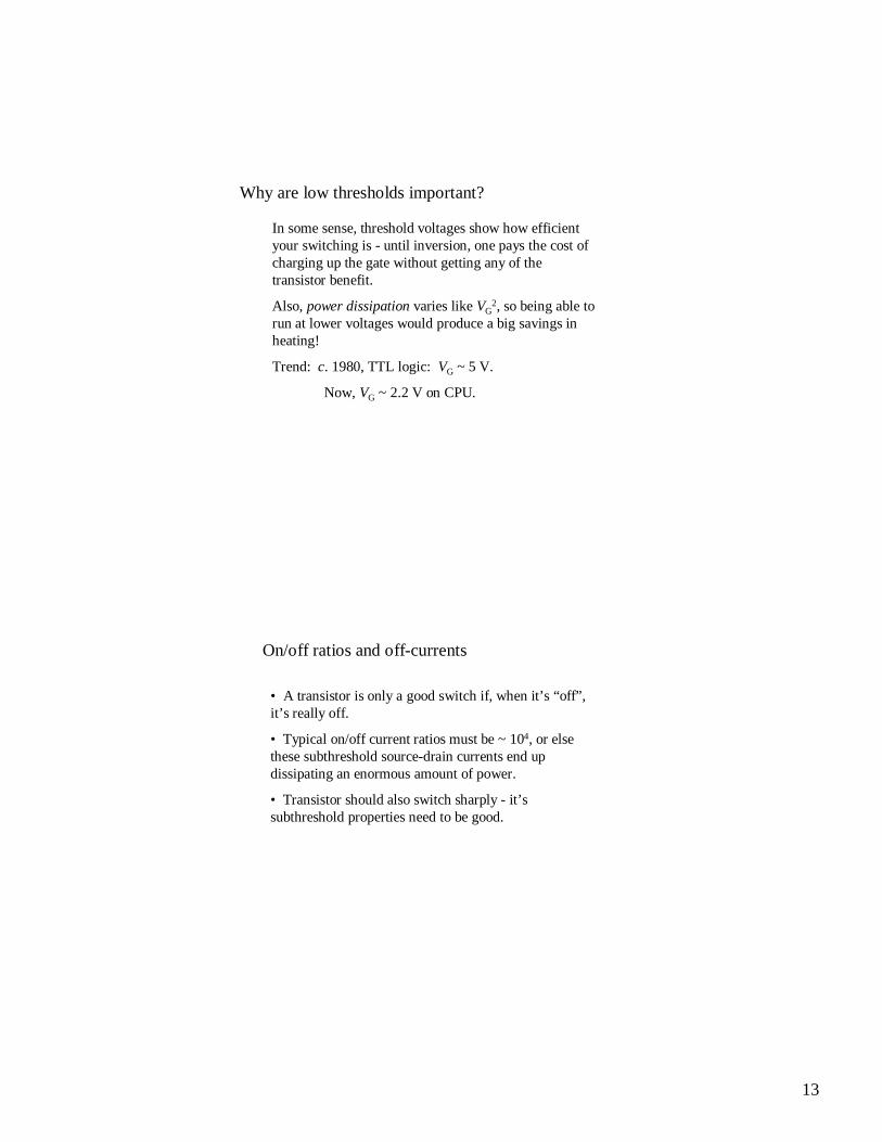
Why are low thresholds important?
In some sense, threshold voltages show how efficient your switching is - until inversion, one pays the cost of charging up the gate without getting any of the transistor benefit.
Also, power dissipation varies like VG2, so being able to
run at lower voltages would produce a big savings in heating!
Trend: c. 1980, TTL logic: VG ~ 5 V.
Now, VG ~ 2.2 V on CPU.
On/off ratios and off-currents
• A transistor is only a good switch if, when it’s “off”, it’s really off.
• Typical on/off current ratios must be ~ 104, or else these subthreshold source-drain currents end up dissipating an enormous amount of power.
• Transistor should also switch sharply - it’s subthreshold properties need to be good.
14
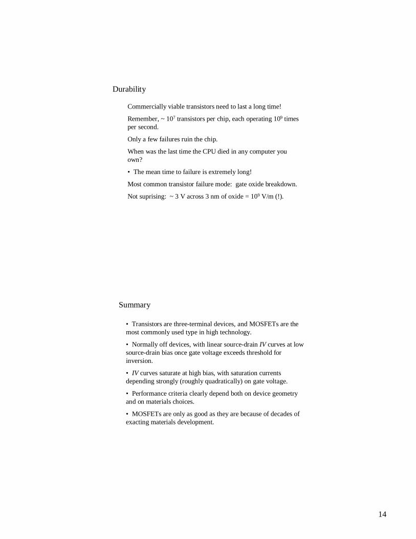
Durability
Commercially viable transistors need to last a long time!
Remember, ~ 107 transistors per chip, each operating 109 times per second.
Only a few failures ruin the chip.
When was the last time the CPU died in any computer you own?
• The mean time to failure is extremely long!
Most common transistor failure mode: gate oxide breakdown.
Not suprising: ~ 3 V across 3 nm of oxide = 109 V/m (!).
Summary
• Transistors are three-terminal devices, and MOSFETs are the most commonly used type in high technology.
• Normally off devices, with linear source-drain IV curves at low source-drain bias once gate voltage exceeds threshold for inversion.
• IV curves saturate at high bias, with saturation currents depending strongly (roughly quadratically) on gate voltage.
• Performance criteria clearly depend both on device geometry and on materials choices.
• MOSFETs are only as good as they are because of decades of exacting materials development.
15
Next time:
• Demands of the electronics industry for high performance transistors.
• The semiconductor “roadmap”, and signs of trouble ahead.
1
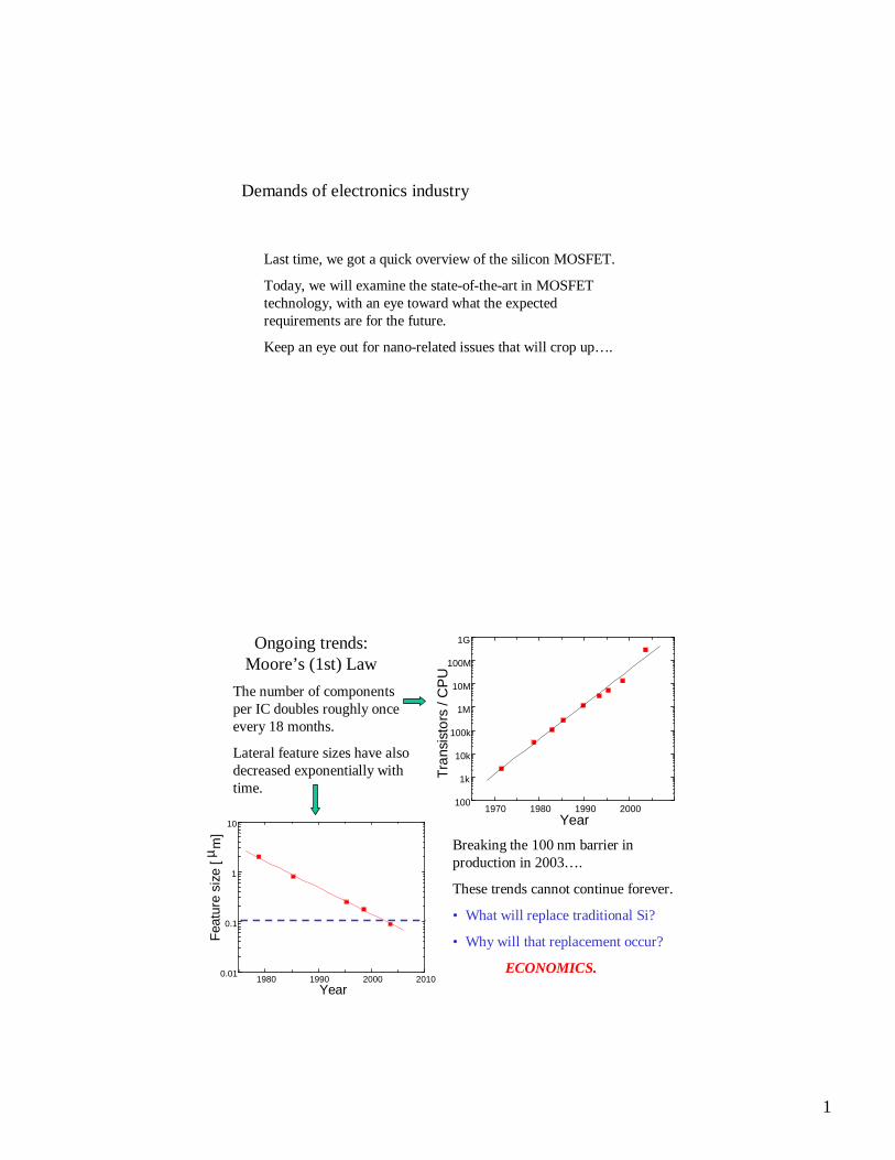
Demands of electronics industry
Last time, we got a quick overview of the silicon MOSFET.
Today, we will examine the state-of-the-art in MOSFET technology, with an eye toward what the expected requirements are for the future.
Keep an eye out for nano-related issues that will crop up….
Ongoing trends: Moore’s (1st) Law
1970 1980 1990 2000100
1k
10k
100k
1M
10M
100M
1G
Tra
nsis
tors
/ C
PU
Year
1980 1990 2000 20100.01
0.1
1
10
Fea
ture
siz
e [µ
m]
Year
The number of components per IC doubles roughly once every 18 months.
Lateral feature sizes have also decreased exponentially with time.
Breaking the 100 nm barrier in production in 2003….
These trends cannot continue forever.
• What will replace traditional Si?
• Why will that replacement occur?
ECONOMICS.
2
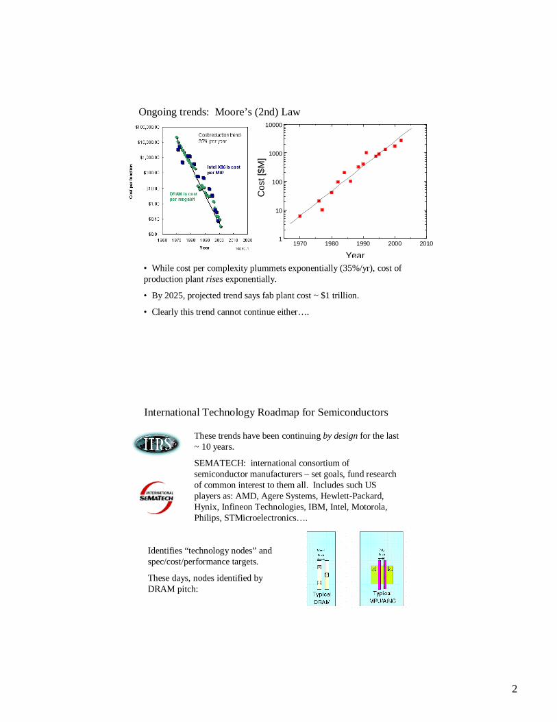
Ongoing trends: Moore’s (2nd) Law
1970 1980 1990 2000 20101
10
100
1000
10000
Cos
t [$M
]Year
• While cost per complexity plummets exponentially (35%/yr), cost of production plant rises exponentially.
• By 2025, projected trend says fab plant cost ~ $1 trillion.
• Clearly this trend cannot continue either….
International Technology Roadmap for Semiconductors
These trends have been continuing by design for the last ~ 10 years.
SEMATECH: international consortium of semiconductor manufacturers – set goals, fund research of common interest to them all. Includes such US players as: AMD, Agere Systems, Hewlett-Packard,Hynix, Infineon Technologies, IBM, Intel, Motorola, Philips, STMicroelectronics….TSMC, and Texas Instruments
Identifies “technology nodes” and spec/cost/performance targets.
These days, nodes identified by DRAM pitch:
3
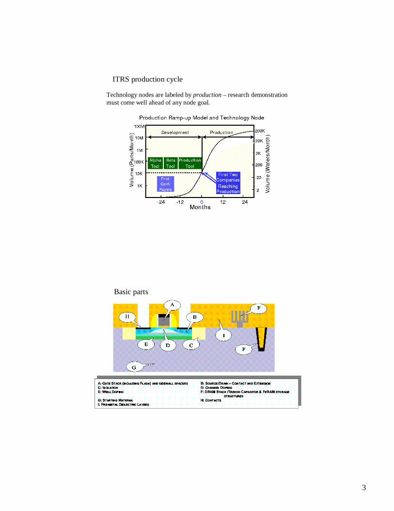
ITRS production cycle
Technology nodes are labeled by production – research demonstration must come well ahead of any node goal.
Basic parts

4
Current production factoids:
• Typical Pentium: ~ 107 transistors, total chip area of 310 mm2
• Active area of transistors is ~ 28 mm2
• Cost per transistor currently between 50 and 100 microcents (!).
• Total number of processing steps needed for one chip: hundreds
• Total number of masks needed for one chip: ~ 30-40
• Acceptable total yield ~ 50% (!)
State-of-the-art: Si material
Growth method: Czochralski
• A seed crystal is attached to slowly rotating rod, and is dipped into Si at just over the melting point.• The rod is slowly withdrawn from the melt.• Rate is increased at end to avoid impurity contamination.
http://www.techfak.uni-kiel.de/matwis/amat/elmat_en/kap_5/illustr/i5_1_1.html
Diameter: 300 mm
Specs needed for 99% good wafers:
Site flatness: < 130 nmNumber of particles: < 120/waferSurface metal contamination: < 1010 at/cm2
Iron concentration: < 1010 at/cm3
Stacking faults: < 1/cm2
5
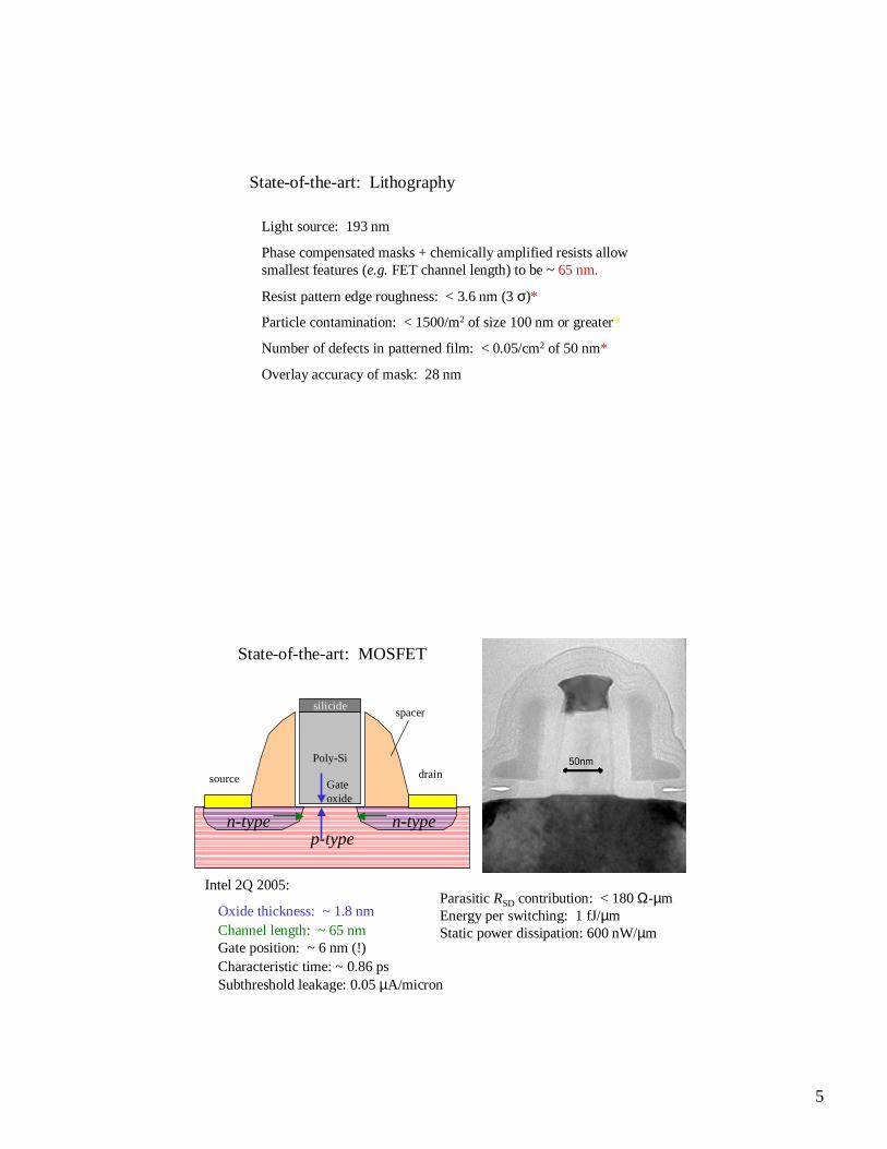
State-of-the-art: Lithography
Light source: 193 nm
Phase compensated masks + chemically amplified resists allow smallest features (e.g. FET channel length) to be ~ 65 nm.
Resist pattern edge roughness: < 3.6 nm (3 σ)*
Particle contamination: < 1500/m2 of size 100 nm or greater*
Number of defects in patterned film: < 0.05/cm2 of 50 nm*
Overlay accuracy of mask: 28 nm
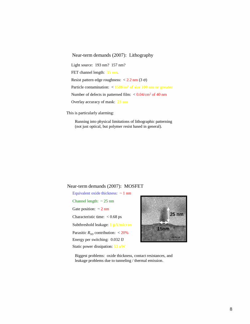
State-of-the-art: MOSFET
p-type
Poly-Si
silicide
n-type n-type
spacer
source drainGate oxide
Oxide thickness: ~ 1.8 nmChannel length: ~ 65 nmGate position: ~ 6 nm (!)Characteristic time: ~ 0.86 psSubthreshold leakage: 0.05 µA/micron
Intel 2Q 2005:Parasitic RSD contribution: < 180 Ω-µmEnergy per switching: 1 fJ/µmStatic power dissipation: 600 nW/µm
6
State-of-the-art: power
• Supply voltage in processor core: ~ 1.1 V
• High performance processor power dissipation (with heatsink): 130 W
• Battery-powered processor power dissipation: 3-5 W
Can crunch some numbers on high-performance system.
Say 107 transistors running at 2.5 GHz gives that 130 W figure.
Now consider 108 transistors in the same area, operating at 10 GHz, for example. Such a processor made with present-day designs and approaches would dissipate ~ 5 kW / cm2 (!!) This is comparable to the power density radiated by a rocket engine….
State-of-the-art: reliability
Device early failures (in first 4000 hours): 50 ppm
Long-term failures (in first 109 hours): 10-100 ppm
Electrostatic protection survival: 10 V/µm
Testing is done under “accelerated failure” conditions –typically running devices at higher-than-normal temperatures, for example.
7
Reading the roadmap
• White = manufacturable solutions known and being optimized.
• Yellow = manufacturable solutions known and demonstrated, but not yet in practice (often, too expensive / yields too low / too new to be optimized yet).
• Red = “brick wall” = no known manufacturable (!) solution to given problem / means of meeting criterion.
Remember the ramp-up cycle. If there’s a red item and it’s less than two years away, the issue is a very serious one.
Roadmap goes out ~ 10 years, but is constantly under revision.
Near-term demands (2007): Si material
Site flatness: < 64 nm (critical, but hard to measure)
Number of particles: < 123/wafer (below measurable threshold)
Surface metal contamination: < 1010 at/cm2 (more critical)
Iron concentration: < 1010 at/cm3 (more critical)
Stacking faults: < 0.3/cm2 (factor of 3 over current)
General trends:
• Even when current tolerances don’t change by much, their importance increases.
• Running into metrology problems - don’t have adequate tools to efficiently assess whether criteria are being met.
8
Near-term demands (2007): Lithography
Light source: 193 nm? 157 nm?
FET channel length: 35 nm.
Resist pattern edge roughness: < 2.2 nm(3 σ)
Particle contamination: < 1500/m2 of size 100 nm or greater
Number of defects in patterned film: < 0.04/cm2 of 40 nm
Overlay accuracy of mask: 23 nm
This is particularly alarming:
Running into physical limitations of lithographic patterning (not just optical, but polymer resist based in general).
Near-term demands (2007): MOSFETEquivalent oxide thickness: ~ 1 nm
Channel length: ~ 25 nm
Gate position: ~ 2 nm
Characteristic time: < 0.68 ps
Subthreshold leakage: 1 µµµµA/micron
Parasitic RSD contribution: < 20%
Energy per switching: 0.032 fJ
Static power dissipation: 53 nW
25 nm
15nm
Biggest problems: oxide thickness, contact resistances, and leakage problems due to tunneling / thermal emission.
9
Long-term demands (2016): Si material
Wafer size (!): 450 mm (How does one grow and polish these?)
Site flatness: < 23 nm
Number of particles: < 75/wafer (below measurable threshold)
Surface metal contamination: < 1010 at/cm2 (more critical)
Iron concentration: < 1010 at/cm3 (more critical)
Stacking faults: < 0.06/cm2 (another factor of 5)
• Most requirements continue increasing criticality.
• Metrology even more of a problem.
• Larger wafer size desired, but may not happen….
Long-term demands (2016): Lithography
Light source: X-ray? E-beam? Imprint?
FET channel length: 9 nm.
Resist pattern edge roughness: < 0.7 nm(3 σ)
Particle contamination: < 500/m2 of size 50 nm or greater
Number of defects in patterned film: < 0.01/cm2 of 10 nm
Overlay accuracy of mask: 9 nm
Noone knows how to do this.
Biggest problems:
• Single-nm alignments across ~ 2cm chip, + across 450 mm wafers.
• Metrology.
10
Long-term demands (2016): MOSFETs
Equivalent oxide thickness: ~ 0.4 nm
Channel length: ~ 9 nm
Characteristic time: < 0.15 ps
Subthreshold leakage: 0.5 µA/micron
Parasitic RSD contribution: < 35%
Energy per switching: 0.285 fJ/µm
Static power dissipation: 4.4 µW/µm
• Intel can make THz, 10 nm channel transistors, but not in bulk.
• Several finite-size problems crop up (contact resistances again)
• Irreversibly changing “1” to “0” costs, minimally, kBT ln 2 = 0.002 fJ (!)
General observations
• We’re running out of time fast for standard CMOS processing if we want to continue Moore’s (1st) law.
• At the nm scale, lack of (fast) metrology is a real killer.
• Not all coming problems are “simple” engineering or process development issues: “We have entered the era of material limited device scaling”.
• We’re approaching the era of physics-limited device scaling in certain aspects as well.
11
Is industry considering alternatives?
The 2001 ITRS was the first roadmap to include a section on Emerging Research Devices.
Planners well aware that they need to be looking at:
• “Nonclassical CMOS” (Transport-enhanced/ultrathin body/source-drain engineered /double-gate/vertical MOSFETs)
• Alternative devices (single-electron transistors)
• Hybrid devices (nanotube FETs)
• Novel architectures (defect tolerance, cellular automata, biologically inspired)
• Really novel architectures (molecular computers, quantum computers)
Roles for “nano”
Pure research
Applied research
• Fundamental physics and chemistry of these materials at nm scale.
• Understanding new phenomena as they arise / become relevant.
• Learning the science of possible new architectures.
• Nanomaterials including resists.
• Metrology: how do you measure critical properties on these length scales?
12
Summary and conclusions
• Moore’s Laws are obeyed by design, not by accident.
• Electronics industry wants to continue aggressive scaling, but faces many challenges along the way.
• “Nano” can and must play a role in addressing these challenges / opportunities.
• Either we’ll make some significant paradigmatic shift within 10-15 years, or computer hardware performance will plateau (e.g. passenger airplane speeds).
• One of the major limiting problems is economic.
Next time:
MOSFET scaling in detail: what’s the physics?