specification transient voltage...tsd 0201 150 nbmb1 engineer specification version: a0 page 10 of...
TRANSCRIPT

INPAQ
Global RF/Component Solutions
Specification TSD 0201 150 NBMB1
Product Name Transient Voltage Suppressor
Series TVS Series
Part No TSD 0201 150 NBMB1
Package Size EIA 0201

INPAQ
Global RF/Component Solutions
TSD 0201 150 NBMB1 Engineer Specification Version: A0 Page 1 of 10
All Specifications are subject to change without notice. www.inpaq.com.tw ; www.inpaqgp.com
TSD 0201 150 NBMB1 Engineering Specification
1. Scope TSD 0201 150 NBMB1 is a TVS diode designed to protect one power/control line or one signal line
from overvoltage hazard of Electrostatic Discharge (ESD). 1.1 GENERAL DESCRIPTION
TSD 0201 150 NBMB1 is a silicon base in ultra small Surface-Mounted Device (SMD) special packages. It is designed to protect sensitive electronics from damage or latch up due to Electrostatic Discharge (ESD), lightning, and other voltage induced transient events.
1.2 FEATURES Bi-directional ESD Protection of one line. Max ESD protection 30 KV IEC 61000-4-2, level 4 (ESD) Low clamping voltage: VCL = 8.5 V (1 A, tp=8/20us) Ultra small SMD special packages
1.3 APPLICATIONS Cellular handsets and accessories Audio and video equipment Communication systems Portable electronics Computers and peripherals
2. Explanation of Part Number
TS D 0201 1 50 N BMB1 (1) (2) (3) (4) (5) (6) (7)
1. Product Type:TVS Diode 2. Package : D: DFN package 3. Package Size Code 4. Channel Code:1=1 Channels 5. Working Voltage: 50 : 5.0 V 6. Capacitance Code:N 7. Specialized Specification Code

INPAQ
Global RF/Component Solutions
TSD 0201 150 NBMB1 Engineer Specification Version: A0 Page 2 of 10
All Specifications are subject to change without notice. www.inpaq.com.tw ; www.inpaqgp.com
3. . Circuit Diagram & Dimension
4. Specifications 4.1. ABSOLUTE MAXIMUM RATINGS
PARAMETER PARAMETER RATING UNITS Operating Supply Voltage VDC 5.0 V
Operating Temperature range To -40 ~ +85 oC
Storage Temperature range TS -55 ~ +125 oC
Lead Soldering Temperature TSOL 260 (10 sec.) oC
4.2. ESD standards compliance
PARAMETER PARAMETER RATING
UNITS MIN TYP MAX
ESD per IEC 61000-4-2 (Contact) VESD ±20 ±30 kV
ESD per IEC 61000-4-2 (Air) VESD ±20 kV
Peak Pulse Current Ipp 10 A

INPAQ
Global RF/Component Solutions
TSD 0201 150 NBMB1 Engineer Specification Version: A0 Page 3 of 10
All Specifications are subject to change without notice. www.inpaq.com.tw ; www.inpaqgp.com
4.3. ELECTRICAL CHARACTERISTICS ELECTRICAL CHARACTERISTICS
PARAMETER SYMBOL CONDITIONS MINI TYP MAX UNITS
Reverse Stand-Off Voltage
VRWM T=25 oC. -5 5 V
Reverse Leakage Current
ILeak VRWM = 5V, T=25 oC. 100 1000 nA
Reverse Breakdown Voltage
VBV IBV = 1mA, T=25 oC. 6 7 V
Clamping Voltage VCL IPP=1A, tp=8/20us, T=25 oC. 8.5 V
Clamping Voltage VCL IPP=3A, tp=8/20us, T=25 oC. 9.6 V
Clamping Voltage VTLP_CL ITLP = 5 A 8 V
Clamping Voltage VTLP_CL ITLP = 16 A 11 V
Diode Capacitance
Cp VR = 0V, f = 1MHz, T=25 oC. 18 pF
Dynamic resistance RDYN between ITLP1 = 2 A and ITLP2 = 15 A
0.2 Ω
4.4. TYPICAL CHARACTERISTICS

INPAQ
Global RF/Component Solutions
TSD 0201 150 NBMB1 Engineer Specification Version: A0 Page 4 of 10
All Specifications are subject to change without notice. www.inpaq.com.tw ; www.inpaqgp.com

INPAQ
Global RF/Component Solutions
TSD 0201 150 NBMB1 Engineer Specification Version: A0 Page 5 of 10
All Specifications are subject to change without notice. www.inpaq.com.tw ; www.inpaqgp.com

INPAQ
Global RF/Component Solutions
TSD 0201 150 NBMB1 Engineer Specification Version: A0 Page 6 of 10
All Specifications are subject to change without notice. www.inpaq.com.tw ; www.inpaqgp.com
5. Taping Package and Label Marking 5.1. Packaging method
Products shall be heat-sealed in the chip pocket, spacing pitch 4-mm of paper carrier tape with cover tape, and the carrier tape shall be reeled to the reel.
5.2. Carrier tape dimensions
Unit: mm

INPAQ
Global RF/Component Solutions
TSD 0201 150 NBMB1 Engineer Specification Version: A0 Page 7 of 10
All Specifications are subject to change without notice. www.inpaq.com.tw ; www.inpaqgp.com
5.3. Taping reel dimensions
5.4 Taping specifications
There shall be the portion having no product in both the head and the end of taping, and there shall be the cover tape in the head of taping.
5.5 Label Marking The label specified as follows shall be put on the side of reel. (1) Part No. (2) Quantity (3) Lot No. *Part No. And Quantity shall be marked on outer packaging.
5.6 Quantity of products in the taping package (1) Standard quantity:15000pcs/Reel for TVS0201 Series (2) Shipping quantity is a multiple of standard quantity.
5.6 Storage Condition with package Storage Time: 12 months max Storage Temperature : 5 to 30℃ Relative Humidity: to 60 %
INPAQ
Global RF/Component Solutions
TSD 0201 150 NBMB1 Engineer Specification Version: A0 Page 8 of 10
All Specifications are subject to change without notice. www.inpaq.com.tw ; www.inpaqgp.com
6. Precautions for Handling
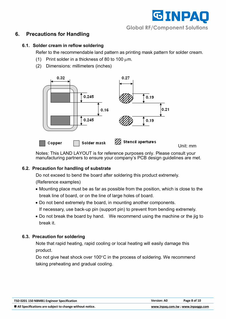
6.1. Solder cream in reflow soldering Refer to the recommendable land pattern as printing mask pattern for solder cream. (1) Print solder in a thickness of 80 to 100 m. (2) Dimensions: millimeters (inches)
Unit: mm Notes: This LAND LAYOUT is for reference purposes only. Please consult your manufacturing partners to ensure your company’s PCB design guidelines are met.
6.2. Precaution for handling of substrate Do not exceed to bend the board after soldering this product extremely. (Reference examples) Mounting place must be as far as possible from the position, which is close to the
break line of board, or on the line of large holes of board. Do not bend extremely the board, in mounting another components.
If necessary, use back-up pin (support pin) to prevent from bending extremely. Do not break the board by hand. We recommend using the machine or the jig to
break it.
6.3. Precaution for soldering Note that rapid heating, rapid cooling or local heating will easily damage this product. Do not give heat shock over 100C in the process of soldering. We recommend taking preheating and gradual cooling.

INPAQ
Global RF/Component Solutions
TSD 0201 150 NBMB1 Engineer Specification Version: A0 Page 9 of 10
All Specifications are subject to change without notice. www.inpaq.com.tw ; www.inpaqgp.com
6.4. Recommendable reflow soldering
Reference IPC-020c-5-1 Profile Feature Pb free Assembly Average Ramp Rate (Ts max to Tp)
3 /second max℃
Preheat - Temperature Min (Tsmin) - Temperature Min (Tsmax) - Time(tsmin to tsmin)
150℃ 200℃ 60-180 seconds
Time maintained above: - Temperature (TL) - Time (tL)
217℃ 60-150 seconds
Peak Temperature (Tp)
260 +0/℃ -5 ℃
Time within 5 of actua℃ l Peak Temperature (Tp)
20-40 seconds
Ramp-Down Rate 6 /second max.℃ Time 25 to Peak Temperature℃ 8 minutes max
INPAQ
Global RF/Component Solutions
TSD 0201 150 NBMB1 Engineer Specification Version: A0 Page 10 of 10
All Specifications are subject to change without notice. www.inpaq.com.tw ; www.inpaqgp.com
6.5. Soldering gun procedure Note the follows, in case of using solder gun for replacement. (1) The tip temperature must be less than 350C for the period within 5 seconds by
using soldering gun less than 30 W. (2) The soldering gun tip shall not touch this product directly.
6.6. Soldering volume Note that excess of soldering volume will easily get crack the body of this product.