transient-thermo-reflectance for the study of surface ... · pdf fileen este trabajo...
TRANSCRIPT
ÓPTICA PURA Y APLICADA. www.sedoptica.es
Opt. Pura Apl. 46 (1) 13-19 (2013) - 13 - © Sociedad Española de Óptica
Sección Especial / Special Section: MOPM - Mexican Optics and Photonics Meeting
Transient-thermo-reflectance for the study of surface carrier dynamics
Reflectancia-termo-transitoria para el estudio de la dinámica de portadores
de carga en superficies
B.G. Pérez-Hernández(A), J. Garduño-Mejía(*,A), C. J. Román-Moreno(A),
O. G. Morales-Saavedra, J. G. Bañuelos-Muñetón, R. Ortega-Martínez(A) CCADET-UNAM, Apdo, Postal 70-186, C.P. 04510. Coyoacán, Cd. Universitaria, México D.F., México.
(*) Email: [email protected] A: miembro de AMO / AMO member
Recibido / Received: 06/09/2012. Revisado / Revised: 13/12/2012. Aceptado / Accepted: 18/12/2012.
DOI: http://dx.doi.org/10.7149/OPA.46.1.13
ABSTRACT:
In this work we present a non-destructive examination (NDE) pump-probe technique known as transient-thermo-reflectance (TTR) for the study of transient carrier dynamics in semiconductor and metal surfaces at low fluence regime. The technique enables to measure the change in reflectance at the sample surface as a function of time on the femtosecond time regime. Changes in reflectance can then be used to determine properties of the sample. Experimental results are compared with numerical model calculations.
Key words: Ultrafast Optics, Femtosecond Time Resolved Spectroscopy.
RESUMEN:
En este trabajo presentamos una técnica no destructiva de bombeo-prueba, técnica conocida como reflectancia termo-transitoria (TTR) para el estudio de la dinámica de portadores de carga en superficies metálicas y semiconductoras a un régimen de fluencia baja. La técnica permite medir el cambio en la reflectancia en la superficie de la muestra como función del tiempo en el régimen temporal de femtosegundos. Los cambios en la reflectancia pueden emplearse para determinar las propiedades de la muestra. Los resultados experimentales se comparan con los cálculos de un modelo numérico.
Palabras clave: Óptica Ultrarrápida, Espectroscopia de Resolución Temporal de Femtosegundos.
REFERENCIAS Y ENLACES / REFERENCES AND LINKS
[1]. P. M. Norris, A. P. Caffrey, R. J. Stevens, J. M. Klopf, J. T. McLeskey Jr., A. N. Smith, “Femtosecond pump–probe nondestructive examination of materials”, Rev. Sci. Instrum. 74, 400-406 (2003). DOI
[2]. J. Garduño-Mejía, M. P. Higlett, S. R. Meech, “Modelling the influence of nonthermal electron dynamics in thin and ultrathin gold films”, Chem. Phys. 341, 276–284 (2007). DOI
[3]. J. Garduño-Mejía, M. P. Higlett, S. R. Meech, “Morphology dependent ultrafast electron dynamics in ultrathin gold films”, Surf. Sci. 602, 3125–3130 (2008). DOI
[4]. R. H. M. Groenveld, R. Sprink, A. Lagendijk, “Femtosecond spectroscopy of electron-electron and electron-phonon energy relaxation in Ag and Au”, Phys. Rev. B 51, 11433-11445 (1995).
[5]. C. K. Sun, F. Vallee, L. H. Acioli, E. P. Ippen, J. G. Fujimoto, “Femtosecond tunable measurement of electron thermalization in gold”, Phys. Rev. B 50, 15337-15348 (1994). DOI
[6]. B. N. Chichkov, C. Momma, S. Nolte, F. von Alvensleben, A. Tünnermann, “Femtosecond, picosecond and nanosecond laser ablation of solids”, Appl. Phys. A - Mater. 63, 109–115 (1996). DOI
[7]. S. I. Anisimov, B. L. Kapeliovich, T. L. Perelman, “Electron emission from metal surfaces exposed to ultrashort laser pulses”, Soviet Physics - JETP 39, 375-377 (1974).

ÓPTICA PURA Y APLICADA. www.sedoptica.es.
Opt. Pura Apl. 46 (1) 13-19 (2013) - 14 - © Sociedad Española de Óptica
[8]. E. Carpene, “Ultrafast laser irradiation of metals: Beyond the two-temperature model”, Phys. Rev. B 74, 024301 (2006). DOI
[9]. J. Hohlfeld, S. S. Wellershoff, J. Gudde, U. Conrad, V. Jahnke, E. Matthias, “Electron and lattice dynamics following optical excitation of metals”, Chem. Phys. 251, 237-258 (2000). DOI
[10]. S. K. Sundaram, E. Mazur, “Inducing and probing non-thermal transitions in semiconductors using femtosecond laser pulses”, Nat. Mater. 1, 217-224 (2002). DOI
[11]. R. P. Prasankumar, A. J. Taylor, Optical Tecniques for Solid–State Materials Characterization, CRC Press, Taylor and Francis Group, Boca Raton, FL, USA (2012).
[12]. F. Rossi, T. Kuhn, “Theory of ultrafast phenomena in photoexcited semiconductors”, Rev. Mod. Phys. 74, 895-950 (2002). DOI
1. Introduction
Ultrashort pulsed lasers have been
demonstrated to be effective tools for the non-
destructive examination (NDE) of energy
transport properties in thin film samples, in
particular for the investigation of transient
dynamics as well as nonlinear optical properties
in semiconductors and metals. A good
alternative for the NDE pump-probe technique is
known as transient-thermo-reflectance (TTR)
for the study of transient dynamics in
semiconductor and metal materials [1]. The
technique enables to measure the change in
reflectance at the sample surface as a function of
time on a sub-picosecond time scale. Changes in
reflectance can then be used to determine
properties of the sample. In the case of metals,
the change in reflectance is related to changes in
temperature and strain. The transient
temperature profile at the surface is then used to
estimates the rate of energy transfer and
coupling factor between the electron and
phonon as well as the thermal properties of the
material [1-9]. In the case of semiconductors, the
change in the reflectance is related to local
electronic state changes and temperature
[1012].
2. Experimental setup
In TTR technique a femtosecond pulse is split
into an intense heating pulse and a weaker
probe pulse (Fig. 1). The heating pulse is used to
generate the transient event to be observed.
Control of the optical path length of the probe
pulse produces a variable time delay between
the pump and probe pulses. The probe then
takes a snapshot of the reflectance at a specific
experimental time delay relative to the pump,
with a temporal resolution on the order of the
probe pulse duration. In our case the delay line
is capable of producing time steps of 3 fs. Pulses
Fig. 1. Transient-thermo-reflectance experimental setup.

ÓPTICA PURA Y APLICADA. www.sedoptica.es
Opt. Pura Apl. 45 (1) 13-19 (2013) - 15 - © Sociedad Española de Óptica
from a self-mode-locked femtosecond
Ti:sapphire laser delivering 200 fs, 76 MHz,
centered at 810 nm (Coherent MIRA-900) were
divided in the pump and probe with a wedged
window. Typical energy per pulse is about 1.5 nJ.
The pump beam passes through a chopper,
creating a modulated pulse train at a prescribed
frequency of 2 KHz, which will drive the
reference frequency and phase of a lock-in
amplifier.
The non collinear pump and probe beams,
with P polarization, are focused to a spot size of
about 4 m with a 25 mm focal length lens at an
incident angle of 45° from the normal. With this
setup the transient reflectance can be associated
with carrier dynamics in both metals and
semiconductors.
Since the method is non-invasive, it
represents a good alternative for measurements
of thermal properties on thin-layer materials.
3. Results
Time resolved spectroscopy results using the
TTR technique are presented in bulk GaAs and a
5 nm thickness Au sample deposited on a glass
substrate in the low fluence excitation regime.
We divided the analysis for the metal and the
semiconductor.
3.1. Metal
Due to the lattice structure of metals, the
electrons are not localized to particular atoms
but in a gas-like dispersed throughout the metal.
The occupancy, at a particular energy state, is
governed by the Fermi-Dirac distribution.
Energy transfer in metals can be described as
follows: after a femtosecond laser pulse
excitation, electrons are promoted to highly non-
equilibrium states. Following the excitation, the
electron thermalization is established by
collisions between excited electrons and
electrons around the Fermi level. Once thermal
equilibrium among hot electrons is reached its
temperature differs strongly from the lattice
temperature, due the large heat capacity
difference, and then diffusion processes and
electron-phonon coupling takes place and cools
down the electron bath. Finally electrons and
lattice reach thermal equilibrium.
Diffusive electron motion and cooling by
electron–phonon coupling can be well described
by the two-temperature model (TTM) and
solved numerically to predict the time and
spatial dependence ( and ) of electron and
lattice temperature [1-3, 6-9]:
,,
,
tzSTTg
z
TTTK
zt
TTC
lephe
elee
eee
(1)
lephel
l TTgt
TC
, (2)
where the source term is:
2
77.2exp1
94.0,pp
tzRJtzS
. (3)
The model is based on coupled electron-
lattice heat transfer differential equations (Eqs.
(1) and (2)) and source term (Eq. (3)) which
involve different optical properties, such as the
reflectance of the film, , excitation source
parameters and others described in Table I
[2,4,8,9].
Transient optical response is estimated by
the computation of the corresponding transient
dielectric function for a given wavelength. The
dielectric function depends directly on the
Fermi-Dirac distribution function, which
depends on the time-dependent electron
temperature, and density of states evolution
(DOS) of the material [2].
The TTM has been demonstrated to be
consistent in bulk samples but shows some
differences for thin films, below 10 nm. For
Table I Optical, excitation and thermal parameters of the Au.
ge-p Electron-phonon coupling factor
2.67×10¹⁶ W/Km3*
Ce=AeTe Electron heat capacity
Ae=67.96 J/m3 K
Cl Lattice heat capacity 2.5×10⁶ J/m3 K
Ke Electron thermal conductivity
318 W/mK
J Laser fluence 36 J/m2
p Pulse width 200 fs
Optical penetration depth
70 nm
*Bulk value
ÓPTICA PURA Y APLICADA. www.sedoptica.es.
Opt. Pura Apl. 46 (1) 13-19 (2013) - 16 - © Sociedad Española de Óptica
instance, energy rate transfer between electrons
and lattice is governed by the electron-phonon
coupling parameter, ge-ph, which is characteristic
for each material. Some investigations have
suggested that this parameter could depend on
the film thickness and structure [3].
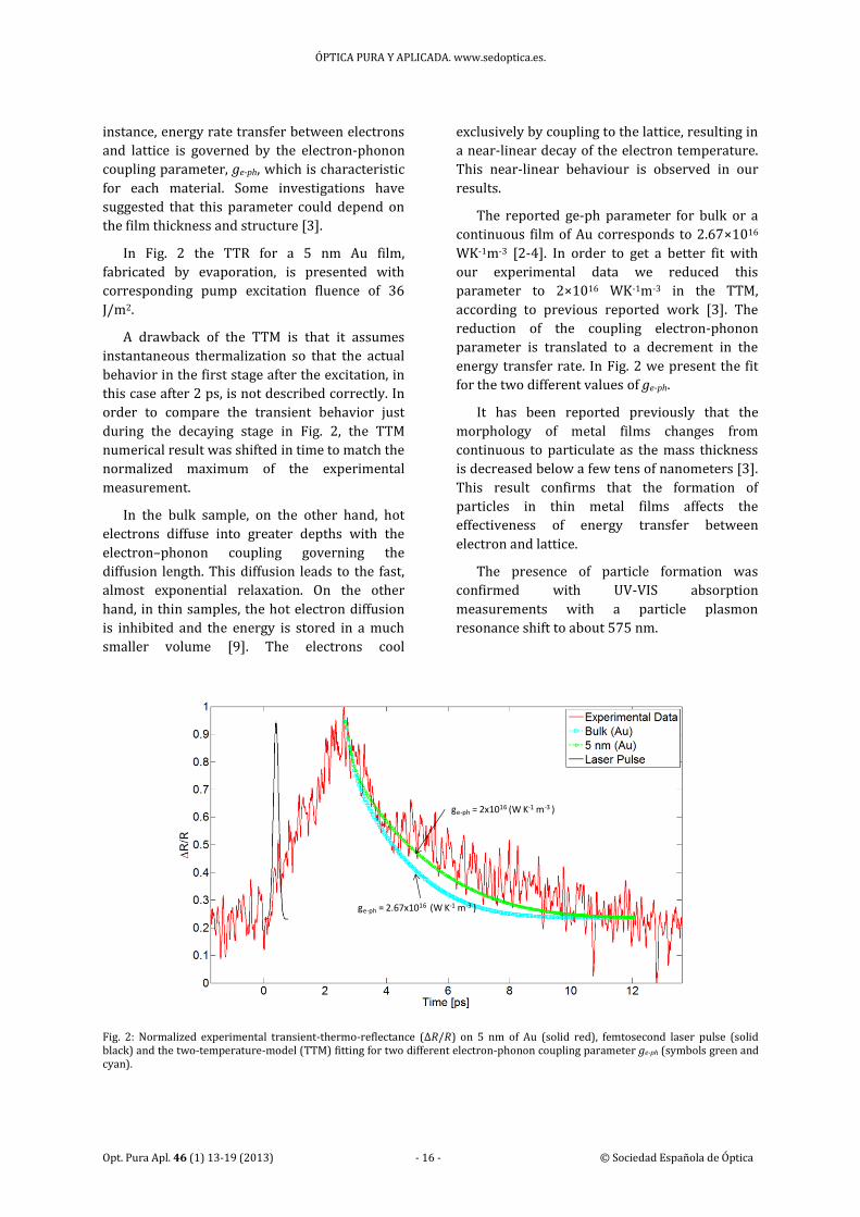
In Fig. 2 the TTR for a 5 nm Au film,
fabricated by evaporation, is presented with
corresponding pump excitation fluence of 36
J/m2.
A drawback of the TTM is that it assumes
instantaneous thermalization so that the actual
behavior in the first stage after the excitation, in
this case after 2 ps, is not described correctly. In
order to compare the transient behavior just
during the decaying stage in Fig. 2, the TTM
numerical result was shifted in time to match the
normalized maximum of the experimental
measurement.
In the bulk sample, on the other hand, hot
electrons diffuse into greater depths with the
electron–phonon coupling governing the
diffusion length. This diffusion leads to the fast,
almost exponential relaxation. On the other
hand, in thin samples, the hot electron diffusion
is inhibited and the energy is stored in a much
smaller volume [9]. The electrons cool
exclusively by coupling to the lattice, resulting in
a near-linear decay of the electron temperature.
This near-linear behaviour is observed in our
results.
The reported ge-ph parameter for bulk or a
continuous film of Au corresponds to 2.67×10¹⁶
WK-1m-3 [2-4]. In order to get a better fit with
our experimental data we reduced this
parameter to 2×10¹⁶ WK-1m-3 in the TTM,
according to previous reported work [3]. The
reduction of the coupling electron-phonon
parameter is translated to a decrement in the
energy transfer rate. In Fig. 2 we present the fit
for the two different values of ge-ph.
It has been reported previously that the
morphology of metal films changes from
continuous to particulate as the mass thickness
is decreased below a few tens of nanometers [3].
This result confirms that the formation of
particles in thin metal films affects the
effectiveness of energy transfer between
electron and lattice.
The presence of particle formation was
confirmed with UV-VIS absorption
measurements with a particle plasmon
resonance shift to about 575 nm.
Fig. 2: Normalized experimental transient-thermo-reflectance on 5 nm of Au (solid red), femtosecond laser pulse (solid black) and the two-temperature-model (TTM) fitting for two different electron-phonon coupling parameter ge-ph (symbols green and cyan).
ge-ph = 2x10¹⁶ (W K-1 m-3 )
ge-ph = 2.67x10¹⁶ (W K-1 m-3 )

ÓPTICA PURA Y APLICADA. www.sedoptica.es.
Opt. Pura Apl. 46 (1) 13-19 (2013) - 17 - © Sociedad Española de Óptica
Fig. 3: UV-VIS absorption data for 5, 10 and 20 nm Au films deposited on a glass surface.
The absorption peak shift is demonstrated in
Fig. 3 where the absorption spectra for 3
different film thicknesses are presented: 5 (TTR
experimental sample), 10 and 20 nm. Actual TTR
experimental results for Au films with
thicknesses of 10 nm and 20 nm have been
presented previously [1,2].
The presence of some structure was also
confirmed with atomic force microscopy
measurements presented in Fig. 4.
Fig. 4: AMF image of the 5 nm Au sample (a) and height histogram (b).
3.2. Semiconductor
On excitation with an ultrashort pulse, a
semiconductor undergoes several stages of
relaxation before returning to equilibrium
[1012]. The energy is transferred first to the
electrons and then to the lattice. The interaction
includes several regimes of carrier excitation
and relaxation as a function of time.
Table II summarizes the hierarchy of the
different regimes as a function of time including
the most relevant interactions [10,11].
Figure 5 illustrates some of the processes
that take place in the regimes of Table I for a
typical direct-gap semiconductor. The various
processes shown do not occur sequentially; they
Fig. 5: Schematic sketch of different recombination processes in bulk semiconductors: (a) band-to-band or direct recombination, (b) exciton recombination, (c) donator-band recombination, (d) acceptor-band recombination, (e) Auger recombination, (f) recombination via deep levels. (a) through d) are radiative recombination processes, where a photon is emitted. (e) and (f) are non-radiative recombination channels.
400 500 600 700 800 900 1000 11000.05
0.1
0.15
0.2
0.25
0.3
0.35
0.4
0.45
0.5
Au Film Thickness [nm]
Wavelength [nm]
Ab
so
rpti
on
20 nm
10 nm
5 nm
6
4
2
00
24
6
m
m
(a)
(b)

ÓPTICA PURA Y APLICADA. www.sedoptica.es
Opt. Pura Apl. 45 (1) 13-19 (2013) - 18 - © Sociedad Española de Óptica
Table II Overview of different temporal regimes of a semiconductor after excitation with an ultrashort laser pulse.
Regime and Timescale Relevant Interaction Remarks
Optical excitation 10-100 fs
Optical dipole moment of interband transitions (or intersubband transitions in quantum structures)
The duration of the excitation pulse is closely related to the energetic width of the excited carrier distribution
Coherent regime 10 fs to several 100 fs
Interaction of optical polarization with electronic states, decay of coherent polarization through scattering processes
Description in terms of coherent wave functions, coherent polarizations, and optical Bloch equations, observation of coherent wavepacket dynamics (quantum beats, Bloch oscillations)
Nonthermal regime <200 fs
Carrier-carrier scattering Carrier distribution cannot be assigned a temperature, occurrence of a spectral hole
Thermalized or hot-carrier regime 100 fs to ps
Carrier-carrier scattering Carrier-phonon interactions
Carrier distribution is defined by a temperature; temperatures of electron and hole distributions may be different and are larger than lattice temperature; temperatures of electron and hole distributions equilibrate with the lattice temperatures
Recombination or isothermal regime ps to μs
Radiative or non-radiative recombination Carrier trapping
Temperatures of carrier distributions and lattice are equal; timescale strongly depends on the material, e.g., direct or indirect semiconductors, density of defects, and quality of surfaces
Fig. 6: Transient-thermo-reflectance response of GaAs (solid blue) and the femtosecond laser pulse (solid black).
0 1 2 3 4 5 6 70
0.2
0.4
0.6
0.8
1Transientent-Thermo-Reflectance results on GaAs
R
/R
Time [ps]
Experimental Data
Fitting
Laser Pulse
Auger recombination
Absorption of photons
Impact ionization
Carrier-carrier scattering
Carrier-phonon scattering
Radiative recombinaition
Carrier diffusion

ÓPTICA PURA Y APLICADA. www.sedoptica.es
Opt. Pura Apl. 45 (1) 13-19 (2013) - 19 - © Sociedad Española de Óptica
overlap in time, forming a continuous chain of events spanning the entire range from
femtoseconds to microseconds. For example,
carriers thermalize at the same time as they cool
by transferring energy to lattice phonons. Non-
thermal structural effects (for example
formation of transient structures) can occur
while the lattice is still cold.
In Fig. 6 we present the TTR technique
applied to GaAs with the description of different
processes which take place at different times,
achieved at an excitation fluence of 36 J/m2.
It has been reported in previous works that
below 0.5 kJ/m2 , or about 50% of the threshold
for irreversible structural change , only
laser-induced lattice heating is produced [10].
With less than one order of magnitude below
this fluence level we were able to generate a
transient thermo reflectance response directly
associated with the thermalization time or hot-
carrier regime. The experimental result was
fitted to the following Eq. (4):
,exp1
expexp1
expexp1
2
21
1
R
RR
Rs
tC
ttB
ttAR
(4)
where is the time delay, is the rise time,
and are the relaxation times, , , are
amplitude parameters and is the fitting result.
Fitting time parameters are listed in Table III.
4. Conclusions
Preliminary results based on femtosecond time-
resolved spectroscopy demonstrates transient
behaviour of the reflectance at the excitation
focal point, which can be related to the change of
Table III Fitting time parameters from TTR experimental results on
GaAs.
Fluence [J/m2]
[ps] [ps] [ps]
36 0.32 0.24 16.27
population of excited carriers on both
semiconductor and metal surfaces. Non-
destructive examination (NDE) of energy
transport technique has been demonstrated in
the low fluence regime of 36 J/m2 with Au and
GaAs. In the case of the Au sample, transient
temperature, heat transfer parameters and
coupling factor related to energy transfer rate
between electrons and phonons were
corroborated with a numerical model.
Comparison between numerical and
experimental results suggest that the formation
of particles in thin Au films, below 10 nm, affects
the effectiveness of energy transfer between
electron and lattice. The nano-structured surface
was demonstrated with UV-VIS spectroscopy
and AFM measurements. For the case of GaAs, at
very low fluence regime, one tenth of the
threshold for irreversible structural changes, we
have demonstrated a transient response with
relaxation times between 240 fs to 16 ps. As far
as we know this is the lowest excitation fluence
that has been reported to achieve transient
thermo reflectance for both metals and
semiconductors.
Acknowledgements
The authors gratefully acknowledge the support
of Dr. M. E. Mata-Zamora for the UV-VIS spectral
measurements and the sponsorship of this work
by DGAPA-UNAM. PAPIIT projects: IN113809,
IB101212, IACOD-1100611, BID-UNAM 98-B3-C-
DGP-L0034-1077 and CONACyT-Mexico project
CB 131746.