tps92691(-q) datasheet - ti.com · connect compensation network to achieve desired closed-5 comp...
TRANSCRIPT

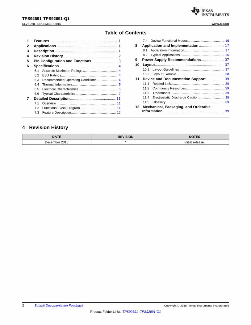
VIN (V)
Effi
cien
cy (
%)
8 9 10 11 12 13 14 15 16 17 1875
80
85
90
95
100
D019
VO = 60 V, ILED = 300 mA
TPS92691-Q1
1
2
3
4
5
6
7
8
16
15
14
13
12
11
10
9
VIN LED+
LEDÅ
VIN
SS
RT/SYNC
PWM
COMP
IADJ
IMON
AGNDPAD
VCC
GATE
IS
PGND
OVP
DDRV
CSP
CSN
L
ROV1
ROV2
RIS
RCS
Q2
Q1
D
CSS
CCOMP
RT
CIMON
COUT
CVCC
CIN
COV
RADJ2
RADJ1
VPWM
Product
Folder
Sample &Buy
Technical
Documents
Tools &
Software
Support &Community
TPS92691, TPS92691-Q1SLVSD68 –DECEMBER 2015
TPS92691/-Q1 Multi-Topology LED Driver With Rail-to-Rail Current Sense Amplifier1 Features 3 Description
The TPS92691/-Q1 is a versatile LED controller that1• Wide Input Voltage: 4.5 V to 65 V
can support a range of step-up or step-down driver• Wide Output Voltage Range: 2 V to 65 V topologies. The device implements a fixed-frequency• Low Input Offset Rail-to-Rail Current Sense peak current mode control technique with
Amplifier programmable switching frequency, slopecompensation, and soft-start timing. It incorporates a– Better than ±3% LED Current Accuracy overhigh voltage (65-V) rail-to-rail current sense amplifier25°C to 140°C Junction Temperature Rangethat can directly measure LED current using either a
– Compatible With High-Side and Low-Side high-side or a low-side series sense resistor. TheCurrent Sense Implementations amplifier is designed to achieve low input offset
voltage and attain better than ±3% LED current• High-Impedance Analog LED Current Adjust Inputaccuracy over junction temperature range of 25°C to(IADJ) With over 15:1 Contrast Ratio140°C and output common-mode voltage range of 0• Over 1000:1 Series FET PWM Dimming Ratio to 60 V.With Integrated Series N-Channel Dim DriverLED current can be independently modulated usingInterfaceeither analog or PWM dimming techniques. Linear• Continuous LED Current Monitor Output foranalog dimming response with 15:1 range is obtainedSystem Fault Detection and Diagnoses by varying the voltage from 140 mV to 2.25 V across
• Programmable Switching Frequency With External the high impedance analog adjust (IADJ) input. PWMClock Synchronization Capability dimming of LED current is achieved by modulating
the PWM input pin with the desired duty cycle and• Programmable Soft-Start and Slopefrequency. Optional DDRV gate driver output can beCompensationused to enable series FET dimming functionality to• Comprehensive Fault Protection Circuitry get over 1000:1 contrast ratio.Including VCC Undervoltage Lockout (UVLO),The TPS92691/-Q1 supports continuous LED statusOutput Overvoltage Protection (OVP), Cycle-by-check through the current monitor (IMON) output.Cycle Switch Current Limit, and ThermalThis allows for LED short circuit or open circuitProtectiondetection and protection. Additional fault protection
• TPS92691-Q1: Automotive Q100 Grade 1 features include VCC UVLO, output OVP, switchQualified cycle-by-cycle current limit, and thermal protection.
2 Applications Device Information(1)
PART NUMBER PACKAGE BODY SIZE (NOM)• TPS92691-Q1: Automotive Exterior LightingTPS92691-Q1Applications HTSSOP (16) 5.10 mm × 6.60 mmTPS92691• Architectural and General Lighting Applications(1) For all available packages, see the orderable addendum at
the end of the data sheet.Typical Boost LED Driver Application Schematic
Efficiency vs Output Voltage
1
An IMPORTANT NOTICE at the end of this data sheet addresses availability, warranty, changes, use in safety-critical applications,intellectual property matters and other important disclaimers. PRODUCTION DATA.
TPS92691, TPS92691-Q1SLVSD68 –DECEMBER 2015 www.ti.com
Table of Contents7.4 Device Functional Modes........................................ 161 Features .................................................................. 1
8 Application and Implementation ........................ 172 Applications ........................................................... 18.1 Application Information............................................ 173 Description ............................................................. 18.2 Typical Applications ................................................ 264 Revision History..................................................... 2
9 Power Supply Recommendations ...................... 375 Pin Configuration and Functions ......................... 310 Layout................................................................... 376 Specifications......................................................... 4
10.1 Layout Guidelines ................................................. 376.1 Absolute Maximum Ratings ...................................... 410.2 Layout Example .................................................... 386.2 ESD Ratings.............................................................. 4
11 Device and Documentation Support ................. 396.3 Recommended Operating Conditions....................... 411.1 Related Links ........................................................ 396.4 Thermal Information .................................................. 511.2 Community Resources.......................................... 396.5 Electrical Characteristics........................................... 511.3 Trademarks ........................................................... 396.6 Typical Characteristics .............................................. 711.4 Electrostatic Discharge Caution............................ 397 Detailed Description ............................................ 1111.5 Glossary ................................................................ 397.1 Overview ................................................................. 11
12 Mechanical, Packaging, and Orderable7.2 Functional Block Diagram ....................................... 11Information ........................................................... 397.3 Feature Description................................................. 12
4 Revision History
DATE REVISION NOTESDecember 2015 * Initial release.
2 Submit Documentation Feedback Copyright © 2015, Texas Instruments Incorporated
Product Folder Links: TPS92691 TPS92691-Q1

1
2
3
4
5
6
7
8
16
15
14
13
12
11
10
9
Thermal Pad
VIN
SS
RT/SYNC
PWM
COMP
IADJ
IMON
AGND
VCC
GATE
IS
PGND
OVP
DDRV
CSP
CSN
TPS92691, TPS92691-Q1www.ti.com SLVSD68 –DECEMBER 2015
5 Pin Configuration and Functions
PWP Package16-Pin HTSSOP with PowerPAD™
Top View
Pin FunctionsPIN
I/O DESCRIPTIONNO. NAME
Input supply for the internal VCC regulator. Bypass with 100-nF capacitor to GND located close to the1 VIN — controller.Soft-start programming pin. Connect a capacitor to AGND to extend the start-up time. Switching can2 SS I/O be disabled by shorting the pin to GND.Oscillator frequency programming pin. Connect a resistor to AGND to set the switching frequency. The
3 RT/SYNC I/O internal oscillator can be synchronized by coupling an external clock pulse through 100-nF seriescapacitor.PWM dimming input. Driving the pin below 2.3 V (typ), turns off switching, idles the oscillator,disconnects the COMP pin, and sets DDRV output to ground. The input signal duty cycle controls the4 PWM I average LED current through PWM dimming operation. Connect to VCC when not used for PWMdimming.Transconductance error amplifier output. Connect compensation network to achieve desired closed-5 COMP I/O loop response.LED current reference input. Connecting pin to VCC with 100-kΩ series resistor sets internal reference
6 IADJ I voltage to 2.42 V and the current sense threshold, V(CSP-CSN)to 172 mV. The pin can be modulated byexternal voltage source from 0 V to 2.25 V to implement analog dimming.LED current report pin. The LED current sensed by CSP/CSN input is reported as VIMON = 14 × ILED ×7 IMON O Rcs. Bypass with a 1-nF ceramic capacitor to AGND.Analog ground. Return for the internal voltage reference and analog circuit. Connect to circuit ground,8 AGND — GND, to complete return path.Current sense amplifier negative input (–). Connect directly to the negative node of LED current sense9 CSN I resistor RCS).Current sense amplifier positive input (+). Connect directly to the positive node of LED current sense10 CSP I resistor RCS).Series dimming FET gate driver output. Connect to gate of external N-channel MOSFET or a level-shift11 DDRV O circuit with P-channel MOSFET to implement series FET PWM dimming.Hysteretic overvoltage protection input. Connect resistor divider from output voltage to set OVP12 OVP I threshold and hysteresis.Power ground connection pin for internal N-channel MOSFET gate drivers. Connect to circuit ground,13 PGND — GND, to complete return path.Switch current sense input. Connected to the switch current sense resistor, RIS, in the source of the N-14 IS I channel MOSFET.
15 GATE O N-channel MOSFET gate driver output. Connect to gate of external switching N-channel MOSFET.VCC bias supply pin. Locally decouple to PGND using a 2.2-µF to 4.7-µF ceramic capacitor located16 VCC — close to the controller.The AGND and PGND pin must be connected to the exposed PowerPAD for proper operation. ThisPowerPAD — PowerPAD must be connected to PCB ground plane using multiple vias for good thermal performance.
Copyright © 2015, Texas Instruments Incorporated Submit Documentation Feedback 3
Product Folder Links: TPS92691 TPS92691-Q1

TPS92691, TPS92691-Q1SLVSD68 –DECEMBER 2015 www.ti.com
6 Specifications
6.1 Absolute Maximum Ratingsover operating free-air temperature range (unless otherwise noted) (1) (2)
MIN MAX UNITVIN, CSP, CSN –0.3 65 VIADJ, IS, PWM, RT/SYNC –0.3 8.8 V
Input voltageOVP, SS –0.3 5.5 VCSP to CSN (3), PGND –0.3 0.3 VVCC, GATE, DDRV –0.3 8.8 V
Output voltage (4)COMP –0.3 5.0 VIMON — 100 µA
Source currentGATE, DDRV (Pulsed <20 ns) — 500 mA
Sink current GATE, DDRV (Pulsed <20 ns) — 500 mAOperating junction temperature, TJ –40 140 °CStorage temperature, Tstg 150 °C
(1) Stresses beyond those listed under Absolute Maximum Ratings may cause permanent damage to the device. These are stress ratingsonly, which do not imply functional operation of the device at these or any other conditions beyond those indicated under RecommendedOperating Conditions. Exposure to absolute-maximum-rated conditions for extended periods may affect device reliability.
(2) All voltages are with respect to AGND unless otherwise noted(3) Continuous sustaining voltage(4) All output pins are not specified to have an external voltage applied.
6.2 ESD RatingsVALUE UNIT
TPS92691-Q1 IN PWP (HTSSOP) PACKAGEHuman-body model (HBM), per AEC Q100-002, all pins (1) ±2000
Electrostatic All pins except 1, 8, 9, andV(ESD) ±500 Vdischarge 16Charged-device model (CDM), per AEC Q100-011Pins 1, 8, 9, and 16 ±750
TPS92691 IN PWP (HTSSOP) PACKAGEHuman-body model (HBM), per ANSI/ESDA/JEDEC JS-001, all pins (2) ±2000ElectrostaticV(ESD) Vdischarge Charged-device model (CDM), per JEDEC specification JESD22-C101, all pins (3) ±500
(1) AEC Q100-002 indicates that HBM stressing shall be in accordance with the ANSI/ESDA/JEDEC JS-001 specification.(2) JEDEC document JEP155 states that 500-V HBM allows safe manufacturing with a standard ESD control process.(3) JEDEC document JEP157 states that 250-V CDM allows safe manufacturing with a standard ESD control process.
6.3 Recommended Operating Conditionsover operating free-air temperature range (unless otherwise noted)
MIN NOM MAX UNITVIN Supply input voltage 6.5 14 65 VVIN, crank Supply input, battery crank voltage 4.5 VVCSP, VCSN Current sense common mode 0 60 VƒSW Switching frequency 80 700 kHzƒSYNC SYNC frequency 0.8 × ƒsw 1.2 × ƒSW kHzVIADJ Current reference voltage 0.14 VIADJ(CLAMP) VTA Operating ambient temperature –40 125 °C
4 Submit Documentation Feedback Copyright © 2015, Texas Instruments Incorporated
Product Folder Links: TPS92691 TPS92691-Q1

TPS92691, TPS92691-Q1www.ti.com SLVSD68 –DECEMBER 2015
6.4 Thermal InformationTPS92691/-Q1
THERMAL METRIC (1) PWP (HTSSOP) UNIT16 PINS
RθJA Junction-to-ambient thermal resistance 40.8 °C/WRθJC(top) Junction-to-case (top) thermal resistance 26.1 °C/WRθJB Junction-to-board thermal resistance 22.2 °C/WψJT Junction-to-top characterization parameter 0.8 °C/WψJB Junction-to-board characterization parameter 22.0 °C/WRθJC(bot) Junction-to-case (bottom) thermal resistance 2.3 °C/W
(1) For more information about traditional and new thermal metrics, see the Semiconductor and IC Package Thermal Metrics applicationreport, SPRA953.
6.5 Electrical CharacteristicsTJ = –40°C to 140°C, VIN = 14 V, VIADJ = 2.2 V, CVCC = 1 µF, CCOMP = 2.2 nF, RCS = 100 mΩ, RT = 20 kΩ, VPWM = 5 V, no loadon GATE and DDRV (unless otherwise noted) (1)
PARAMETER TEST CONDITIONS MIN TYP MAX UNITINPUT VOLTAGE (VIN)VDO LDO dropout voltage ICC = 20 mA, VIN = 5 V 300 mVBIAS SUPPLY (VCC)VCC(REG) Regulation voltage No load 7.0 7.5 8.0 V
VCC rising threshold, VIN = 8 V 4.1 4.35 VVCC(UVLO) Supply undervoltage protection VCC falling threshold, VIN = 8 V 3.75 4.0 V
Hysteresis 100 mVICC(LIMIT) Supply current limit VCC = 0 V 26 38 46 mAICC(STBY) Supply stand-by current VPWM = 0 V 1.8 2.1 mAICC(SW) Supply switching current VCC = 7.5 V, CGATE = 1 nF 5.1 6.6 mAOSCILLATOR (RT/SYNC)
RT = 40 kΩ 165 200 230 kHzƒSW Switching frequency
RT = 20 kΩ 327 390 448 kHzVRT RT output voltage 1 V
SYNC rising threshold VRT/SYNC rising 2.7 3.1 VVSYNC SYNC falling threshold VRT/SYNC falling 1.8 2 VtSYNC(MIN) Minimum SYNC clock pulse width 100 nsGATE DRIVER (GATE)RGH Gate driver high side resistance IGATE = –10 mA 5.4 11.2 ΩRGL Gate driver low side resistance IGATE = 10 mA 4.3 10.5 ΩCURRENT SENSE (IS)VIS(LIMIT) Current limit threshold 497 525 550 mVtIS(BLANK) Leading edge blanking time 103 150 188 nstIS(FAULT) Current limit fault time 35 µstILMT(DLY) IS to GATE propagation delay VIS pulsed from 0 to 1 V 100 nsPWM COMPARATOR AND SLOPE COMPENSATIONDMAX Maximum duty cycle 90.4% 93% 94.7%VLV IS to COMP level shift voltage No slope compensation added 1.17 1.5 1.8 V
D = DMAX (with max slopeVSL Slope compensation 200 mVcompensation)ILV IS level shift bias current No slope compensation added 25 µA
(1) All voltages are with respect to AGND unless otherwise noted
Copyright © 2015, Texas Instruments Incorporated Submit Documentation Feedback 5
Product Folder Links: TPS92691 TPS92691-Q1
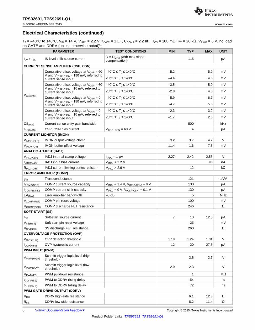
TPS92691, TPS92691-Q1SLVSD68 –DECEMBER 2015 www.ti.com
Electrical Characteristics (continued)TJ = –40°C to 140°C, VIN = 14 V, VIADJ = 2.2 V, CVCC = 1 µF, CCOMP = 2.2 nF, RCS = 100 mΩ, RT = 20 kΩ, VPWM = 5 V, no loadon GATE and DDRV (unless otherwise noted)(1)
PARAMETER TEST CONDITIONS MIN TYP MAX UNITD = DMAX (with max slopeILV + ISL IS level shift source current 115 µAcompensation)
CURRENT SENSE AMPLIFIER (CSP, CSN)Cumulative offset voltage at VCSP = 60 –40°C ≤ TJ ≤ 140°C –5.2 5.9 mVV and V(CSP-CSN) = 150 mV, referred to
25°C ≤ TJ ≤ 140°C –4.4 4.6 mVcurrent sense inputCumulative offset voltage at VCSP = 60 –40°C ≤ TJ ≤ 140°C –3.5 5.0 mVV and V(CSP-CSN) = 10 mV, referred to
25°C ≤ TJ ≤ 140°C -2.8 4.0 mVcurrent sense inputVCS(offset) Cumulative offset voltage at VCSN = 0 –40°C ≤ TJ ≤ 140°C –5.9 6.7 mV
V and V(CSP-CSN) = 150 mV, referred to25°C ≤ TJ ≤ 140°C -4.7 5.0 mVcurrent sense input
Cumulative offset voltage at VCSN = 0 –40°C ≤ TJ ≤ 140°C –2.3 3.2 mVV and V(CSP-CSN) = 10 mV, referred to
25°C ≤ TJ ≤ 140°C –1.7 2.6 mVcurrent sense inputCS(BW) Current sense unity gain bandwidth 500 kHzICS(BIAS) CSP, CSN bias current VCSP, CSN = 60 V 4 µACURRENT MONITOR (IMON)VIMON(CLP) IMON output voltage clamp 3.2 3.7 4.2 VVIMON(OS) IMON buffer offset voltage –11.4 –1.6 7.3 mVANALOG ADJUST (IADJ)VIADJ(CLP) IADJ internal clamp voltage IIADJ = 1 µA 2.27 2.42 2.55 VIIADJ(BIAS) IADJ input bias current VIADJ < 2.2 V 90 nARIADJ(LMT) IADJ current limiting series resistor VIADJ > 2.6 V 12 kΩERROR AMPLIFIER (COMP)gM Transconductance 121 µA/VICOMP(SRC) COMP current source capacity VIADJ = 1.4 V, V(CSP-CSN) = 0 V 130 µAICOMP(SINK) COMP current sink capacity VIADJ = 0 V, V(CSP-CSN) = 0.1 V 130 µAEA(BW) Error amplifier bandwidth –3 dB 5 MHzVCOMP(RST) COMP pin reset voltage 100 mVRCOMP(DCH) COMP discharge FET resistance 246 ΩSOFT-START (SS)ISS Soft-start source current 7 10 12.8 µAVSS(RST) Soft-start pin reset voltage 25 mVRSS(DCH) SS discharge FET resistance 260 ΩOVERVOLTAGE PROTECTION (OVP)VOVP(THR) OVP detection threshold 1.18 1.24 1.31 VIOVP(HYS) OVP hysteresis current 12 20 27.5 µAPWM INPUT (PWM)
Schmitt trigger logic level (highVPWM(HIGH) 2.5 2.7 Vthreshold)Schmitt trigger logic level (lowVPWM(LOW) 2.0 2.3 Vthreshold)
RPWM(PD) PWM pulldown resistance 1 MΩtDLY(RISE) PWM to DDRV rising delay 54 nstDLY(FALL) PWM to DDRV falling delay 72 nsPWM GATE DRIVE OUTPUT (DDRV)RDH DDRV high-side resistance 6.1 12.8 ΩRDL DDRV low-side resistance 5.2 11.4 Ω
6 Submit Documentation Feedback Copyright © 2015, Texas Instruments Incorporated
Product Folder Links: TPS92691 TPS92691-Q1
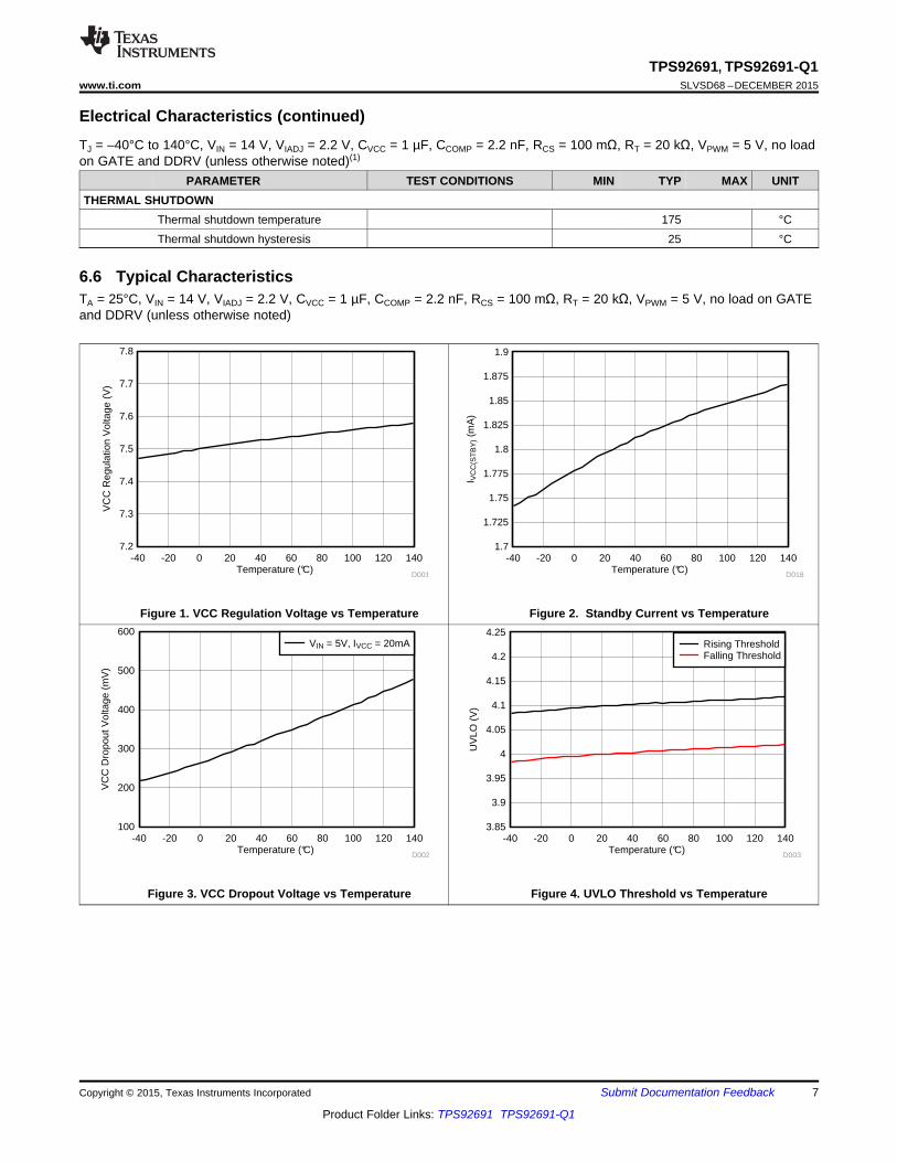
Temperature (°C)
VC
C D
ropo
ut V
olta
ge (
mV
)
-40 -20 0 20 40 60 80 100 120 140100
200
300
400
500
600
D002
VIN = 5V, IVCC = 20mA
Temperature (°C)
UV
LO (
V)
-40 -20 0 20 40 60 80 100 120 1403.85
3.9
3.95
4
4.05
4.1
4.15
4.2
4.25
D003
Rising ThresholdFalling Threshold
Temperature (°C)
VC
C R
egul
atio
n V
olta
ge (
V)
-40 -20 0 20 40 60 80 100 120 1407.2
7.3
7.4
7.5
7.6
7.7
7.8
D001Temperature (°C)
I VC
C(S
TB
Y) (
mA
)
-40 -20 0 20 40 60 80 100 120 1401.7
1.725
1.75
1.775
1.8
1.825
1.85
1.875
1.9
D018
TPS92691, TPS92691-Q1www.ti.com SLVSD68 –DECEMBER 2015
Electrical Characteristics (continued)TJ = –40°C to 140°C, VIN = 14 V, VIADJ = 2.2 V, CVCC = 1 µF, CCOMP = 2.2 nF, RCS = 100 mΩ, RT = 20 kΩ, VPWM = 5 V, no loadon GATE and DDRV (unless otherwise noted)(1)
PARAMETER TEST CONDITIONS MIN TYP MAX UNITTHERMAL SHUTDOWN
Thermal shutdown temperature 175 °CThermal shutdown hysteresis 25 °C
6.6 Typical CharacteristicsTA = 25°C, VIN = 14 V, VIADJ = 2.2 V, CVCC = 1 µF, CCOMP = 2.2 nF, RCS = 100 mΩ, RT = 20 kΩ, VPWM = 5 V, no load on GATEand DDRV (unless otherwise noted)
Figure 1. VCC Regulation Voltage vs Temperature Figure 2. Standby Current vs Temperature
Figure 3. VCC Dropout Voltage vs Temperature Figure 4. UVLO Threshold vs Temperature
Copyright © 2015, Texas Instruments Incorporated Submit Documentation Feedback 7
Product Folder Links: TPS92691 TPS92691-Q1
Temperature (°C)
IS C
urre
nt L
imit
Thr
esho
ld (
mV
)
-40 -20 0 20 40 60 80 100 120 140518
520
522
524
526
528
530
532
D007Temperature (°C)
LEB
Per
iod
(ns)
-40 -20 0 20 40 60 80 100 120 140148
150
152
154
156
158
D008
Temperature (°C)
Sw
itchi
ng F
requ
ency
(kH
z)
-40 -20 0 20 40 60 80 100 120 140382
386
390
394
398
402
D006Temperature (°C)
DM
AX (
%)
-40 -20 0 20 40 60 80 100 120 14092.7
92.8
92.9
93
93.1
93.2
D012
Temperature (°C)
VC
C C
urre
nt L
imit
(mA
)
-40 -20 0 20 40 60 80 100 120 14037
37.5
38
38.5
39
39.5
D004Frequency (kHz)
RT (
k:)
50 150 250 350 450 550 650 75010
20
30
40
50
607080
100
D005
TPS92691, TPS92691-Q1SLVSD68 –DECEMBER 2015 www.ti.com
Typical Characteristics (continued)TA = 25°C, VIN = 14 V, VIADJ = 2.2 V, CVCC = 1 µF, CCOMP = 2.2 nF, RCS = 100 mΩ, RT = 20 kΩ, VPWM = 5 V, no load on GATEand DDRV (unless otherwise noted)
Figure 5. VCC Current Limit vs Temperature Figure 6. RT vs Switching Frequency
Figure 7. Switching Frequency vs Temperature Figure 8. Maximum Duty Cycle vs Temperature
Figure 9. IS Current Limit Threshold vs Temperature Figure 10. Leading Edge Blanking Period vs Temperature
8 Submit Documentation Feedback Copyright © 2015, Texas Instruments Incorporated
Product Folder Links: TPS92691 TPS92691-Q1

VIADJ (V)
V(C
SP
-CS
N) T
hres
hold
(m
V)
0 0.28 0.56 0.84 1.12 1.4 1.68 1.96 2.24 2.52 2.8 30
20
40
60
80
100
120
140
160
180
200
D014Temperature (°C)
VIA
DJ
Vol
tage
Cla
mp
(V)
-40 -20 0 20 40 60 80 100 120 1402.4
2.405
2.41
2.415
2.42
2.425
2.43
2.435
2.44
D015
Temperature (°C)
CS
P, C
SN
Bia
s C
urre
nt (P
A)
-40 -20 0 20 40 60 80 100 120 1403.8
3.85
3.9
3.95
4
4.05
4.1
4.15
4.2
D013V(CSP-CSN) (mV)
VIM
ON (
V)
0 30 60 90 120 150 180 210 240 270 3000
0.5
1
1.5
2
2.5
3
3.5
4
D011
VCSP (V)
V(C
SP
-CS
N) T
hres
hold
(m
V)
0 5 10 15 20 25 30 35 40 45 50 55 60 65149.4
149.6
149.8
150
150.2
150.4
150.6
150.8
151
D009Temperature (°C)
VC
S(O
FF
SE
T) (
mV
)
-40 -20 0 20 40 60 80 100 120 140-0.8
-0.6
-0.4
-0.2
0
0.2
0.4
D010
VCSP = 60VVCSP = 0V
TPS92691, TPS92691-Q1www.ti.com SLVSD68 –DECEMBER 2015
Typical Characteristics (continued)TA = 25°C, VIN = 14 V, VIADJ = 2.2 V, CVCC = 1 µF, CCOMP = 2.2 nF, RCS = 100 mΩ, RT = 20 kΩ, VPWM = 5 V, no load on GATEand DDRV (unless otherwise noted)
VIADJ = 2.1 V VIADJ = 2.1 V
Figure 11. V(CSP-CSN) Threshold vs VCSP Figure 12. Current Sense Amplifier Offset vs Temperature
Figure 13. CSP/CSN Input Bias Current vs Temperature Figure 14. VIMON vs V(CSP-CSN)
Figure 15. V(CSP-CSN) Threshold vs VIADJ Figure 16. VIADJ Voltage Clamp vs Temperature
Copyright © 2015, Texas Instruments Incorporated Submit Documentation Feedback 9
Product Folder Links: TPS92691 TPS92691-Q1

Temperature (°C)
OV
P D
etec
tion
Thr
esho
ld (
V)
-40 -20 0 20 40 60 80 100 120 1401.22
1.225
1.23
1.235
1.24
1.245
1.25
1.255
1.26
D016Temperature (°C)
OV
P H
yste
resi
s C
urre
nt (P
A)
-40 -20 0 20 40 60 80 100 120 14019
19.4
19.8
20.2
20.6
21
D017
TPS92691, TPS92691-Q1SLVSD68 –DECEMBER 2015 www.ti.com
Typical Characteristics (continued)TA = 25°C, VIN = 14 V, VIADJ = 2.2 V, CVCC = 1 µF, CCOMP = 2.2 nF, RCS = 100 mΩ, RT = 20 kΩ, VPWM = 5 V, no load on GATEand DDRV (unless otherwise noted)
Figure 17. OVP Detection Threshold vs Temperature Figure 18. OVP Hysteresis Current vs Temperature
10 Submit Documentation Feedback Copyright © 2015, Texas Instruments Incorporated
Product Folder Links: TPS92691 TPS92691-Q1

QS
R
STANDBY
7.5V LDO Regulator
UVLO (4.1V)
THERMAL LIMIT
INTERNAL REFERENCES
1.24V
CLOCK
OSCILLATOR &
SLOPE
+
+
+
SS
SLOPE
MAX DUTY
10�A+
+
525mV
LEB
LEB
+
1.24V
35 �s TIMER
10�A
20�A
FA
ULT
VCC
PGND
VIN
RT/SYNC
SS
PWM
COMP
CSP
CSN
IMON
IADJ
AGND
PGND
GATE
VCC
OVP
IS
DDRV
STANDBY
138k
2k
FAULT
PWM COMP
3.7V
2.42V
525mV
+
2.42V
12k
FAULT
RESET LOGIC
25mV100mV
SLOPE
CURRENT SENSE AMPLIFIER
GAIN = 14
TPS92691, TPS92691-Q1www.ti.com SLVSD68 –DECEMBER 2015
7 Detailed Description
7.1 OverviewThe TPS92691/-Q1 wide input range (4.5 V to 65 V) controller features all of the functions necessary toimplement a highly efficient and compact LED driver based on step-up or step-down converter topologies. Thedevice implements a fixed-frequency, peak current mode control technique to achieve a constant current output,ideal for driving a single string of series-connected LEDs. The integrated low input offset, rail-to-rail current senseamplifier supports a wide range of output voltages (0 V to 65 V) and is capable of powering an LED stringconsisting of 1 to more than 20 white LEDs. The controller is compatible with either high- or low-side currentshunt sensing technique, based on the LED configuration and driver topology. The LED current sense threshold,set by the analog adjust input, IADJ, provides the capability to analog (amplitude) dim over a linear range of 15:1by varying the voltage, VIADJ, from 140 mV to 2.25 V. The IADJ input provides the means to externally programLED current and facilitates calibration, brightness correction, and thermal management of the LEDs. Highresolution and linear dimming response is achieved by varying the duty cycle of LED current based on the PWMinput. The PWM input directly controls the GATE and DDRV drive outputs, controls the internal oscillator, andenables high-speed PWM dimming with over 1000:1 contrast ratio when using an external MOSFET placed inseries with the LED load. The current monitor output, IMON, reports the instantaneous status of LED currentmeasured by the rail-to-rail current sense amplifier. This feature is incorporated to indicate LED short and open-circuit failures and enables cable harness fault detection independent of LED driver topology. Other faultprotection features include cycle-by-cycle current limiting, hysteresis-based overvoltage protection, VCCundervoltage protection, thermal shutdown, and remote shutdown capability by pulling down the SS pin.
7.2 Functional Block Diagram
Copyright © 2015, Texas Instruments Incorporated Submit Documentation Feedback 11
Product Folder Links: TPS92691 TPS92691-Q1
CC(GATE) G SWI Q f u
RT/SYNC
TPS92691
TRSYNCC OSCILLATOR
CLOCK
� �� �
10
T 1.047SW
1.432 10R
f
u :
TPS92691, TPS92691-Q1SLVSD68 –DECEMBER 2015 www.ti.com
7.3 Feature Description
7.3.1 Internal Regulator and Undervoltage Lockout (UVLO)The IC incorporates a 65-V input VIN rated linear regulator to generate the 7.5 V (typ) VCC bias supply and otherinternal reference voltages. The VCC output is monitored to implement UVLO protection. The device is enabledwhen VCC exceeds the 4.1-V (typ) threshold and is disabled when VCC drops below the 4.0-V (typ) threshold. TheUVLO comparator provides 0.1 V of hysteresis to avoid chatter during transitions. The UVLO thresholds areinternally fixed and cannot be adjusted. The supply current, ICC, is limited to 26 mA minimum to protect thedevice under VCC pin short-circuit conditions. The VCC supply powers the internal circuitry and N-channel gatedriver outputs, GATE, and DDRV. Place a bypass capacitor in the range of 2.2 µF to 4.7 µF across the VCCoutput and PGND to ensure proper operation. The regulator operates in dropout when input voltage VIN fallsbelow 7.5 V forcing VCC to be lower than VIN by 300 mV for a 20-mA supply current. The VCC is a regulatedoutput of the internal regulator and is not recommended to be driven from an external power supply.
7.3.2 OscillatorThe TPS92691/-Q1 switching frequency is programmable by a single external resistor connected between theRT/SYNC pin and the AGND pin. To set a desired frequency, ƒSW (Hz), the resistor value can be calculated fromEquation 1.
(1)
Figure 6 shows a graph of switching frequency versus resistance, RT. TI recommends a switching frequencysetting between 80 kHz and 700 kHz for optimal performance over input and output voltage operating range andfor best efficiency. Operation at higher switching frequencies requires careful selection of N-channel MOSFETcharacteristics and should take into consideration additional switching losses and junction temperature rise.
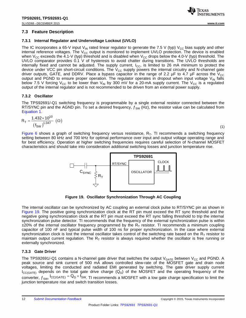
Figure 19. Oscillator Synchronization Through AC Coupling
The internal oscillator can be synchronized by AC coupling an external clock pulse to RT/SYNC pin as shown inFigure 19. The positive going synchronization clock at the RT pin must exceed the RT sync threshold and thenegative going synchronization clock at the RT pin must exceed the RT sync falling threshold to trip the internalsynchronization pulse detector. TI recommends that the frequency of the external synchronization pulse is within±20% of the internal oscillator frequency programmed by the RT resistor. TI recommends a minimum couplingcapacitor of 100 nF and typical pulse width of 100 ns for proper synchronization. In the case where externalsynchronization clock is lost the internal oscillator takes control of the switching rate based on the RT resistor tomaintain output current regulation. The RT resistor is always required whether the oscillator is free running orexternally synchronized.
7.3.3 Gate DriverThe TPS92691/-Q1 contains a N-channel gate driver that switches the output VGATE between VCC and PGND. Apeak source and sink current of 500 mA allows controlled slew-rate of the MOSFET gate and drain nodevoltages, limiting the conducted and radiated EMI generated by switching. The gate driver supply currentICC(GATE) depends on the total gate drive charge (QG) of the MOSFET and the operating frequency of theconverter, ƒSW, . TI recommends a MOSFET with a low gate charge specification to limit thejunction temperature rise and switch transition losses.
12 Submit Documentation Feedback Copyright © 2015, Texas Instruments Incorporated
Product Folder Links: TPS92691 TPS92691-Q1
CSP
CSN
FDMC
FSR
FSR
FCMCFCMC
+
±CSR
TPS92691
Common Mode Filter Capacitors
Differential Mode Filter Capacitors
TPS92691, TPS92691-Q1www.ti.com SLVSD68 –DECEMBER 2015
Feature Description (continued)While choosing the N-channel MOSFET device, consider the threshold voltage when operating in the dropoutregion when VIN is below the VCC regulation level. TI recommends a logic level device with a threshold voltagebelow 5 V when the device is required to operate at an input voltage less than 7 V.
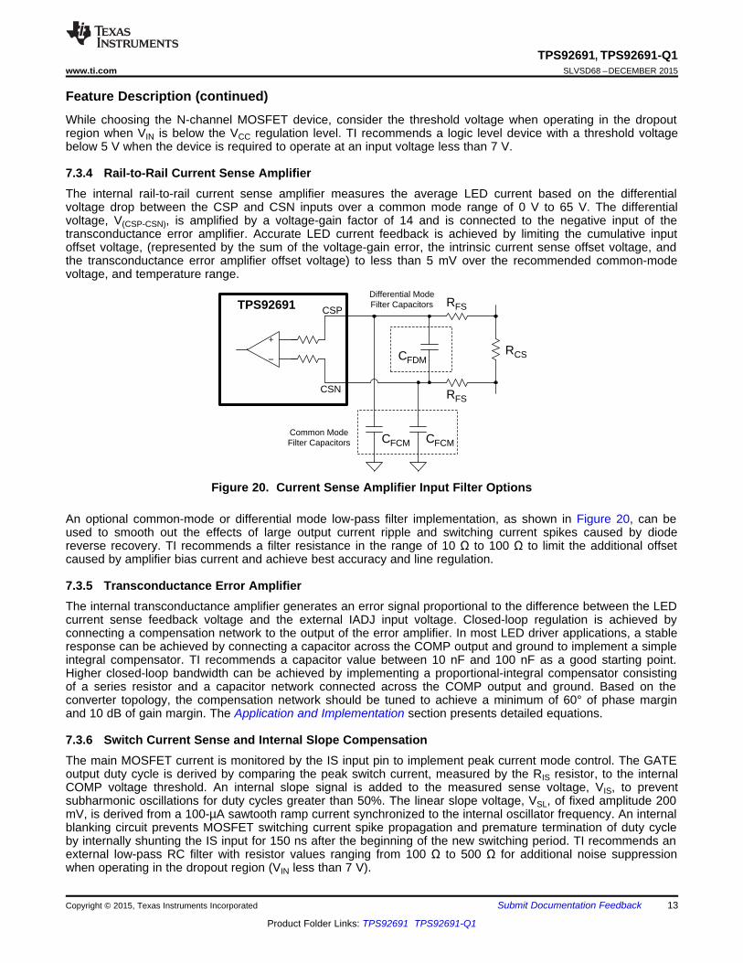
7.3.4 Rail-to-Rail Current Sense AmplifierThe internal rail-to-rail current sense amplifier measures the average LED current based on the differentialvoltage drop between the CSP and CSN inputs over a common mode range of 0 V to 65 V. The differentialvoltage, V(CSP-CSN), is amplified by a voltage-gain factor of 14 and is connected to the negative input of thetransconductance error amplifier. Accurate LED current feedback is achieved by limiting the cumulative inputoffset voltage, (represented by the sum of the voltage-gain error, the intrinsic current sense offset voltage, andthe transconductance error amplifier offset voltage) to less than 5 mV over the recommended common-modevoltage, and temperature range.
Figure 20. Current Sense Amplifier Input Filter Options
An optional common-mode or differential mode low-pass filter implementation, as shown in Figure 20, can beused to smooth out the effects of large output current ripple and switching current spikes caused by diodereverse recovery. TI recommends a filter resistance in the range of 10 Ω to 100 Ω to limit the additional offsetcaused by amplifier bias current and achieve best accuracy and line regulation.
7.3.5 Transconductance Error AmplifierThe internal transconductance amplifier generates an error signal proportional to the difference between the LEDcurrent sense feedback voltage and the external IADJ input voltage. Closed-loop regulation is achieved byconnecting a compensation network to the output of the error amplifier. In most LED driver applications, a stableresponse can be achieved by connecting a capacitor across the COMP output and ground to implement a simpleintegral compensator. TI recommends a capacitor value between 10 nF and 100 nF as a good starting point.Higher closed-loop bandwidth can be achieved by implementing a proportional-integral compensator consistingof a series resistor and a capacitor network connected across the COMP output and ground. Based on theconverter topology, the compensation network should be tuned to achieve a minimum of 60° of phase marginand 10 dB of gain margin. The Application and Implementation section presents detailed equations.
7.3.6 Switch Current Sense and Internal Slope CompensationThe main MOSFET current is monitored by the IS input pin to implement peak current mode control. The GATEoutput duty cycle is derived by comparing the peak switch current, measured by the RIS resistor, to the internalCOMP voltage threshold. An internal slope signal is added to the measured sense voltage, VIS, to preventsubharmonic oscillations for duty cycles greater than 50%. The linear slope voltage, VSL, of fixed amplitude 200mV, is derived from a 100-µA sawtooth ramp current synchronized to the internal oscillator frequency. An internalblanking circuit prevents MOSFET switching current spike propagation and premature termination of duty cycleby internally shunting the IS input for 150 ns after the beginning of the new switching period. TI recommends anexternal low-pass RC filter with resistor values ranging from 100 Ω to 500 Ω for additional noise suppressionwhen operating in the dropout region (VIN less than 7 V).
Copyright © 2015, Texas Instruments Incorporated Submit Documentation Feedback 13
Product Folder Links: TPS92691 TPS92691-Q1
IADJ
TPS92691
ADJ1R
ADJ2R
VCC
IADJ
TPS92691
NTCR
ADJR
VCC
ÅW��
IADJ
TPS92691
ADJC
ADJR
PWM SIGNAL
(a) (b) (c)
TPS92691, TPS92691-Q1SLVSD68 –DECEMBER 2015 www.ti.com
Feature Description (continued)Cycle-by-cycle current limit is accomplished by a redundant internal comparator, which immediately terminatesthe GATE output when the IS input voltage, VIS, exceeds 525-mV (typ) threshold. Upon a current limit event, theSS and COMP pin are internally grounded to reset the state of the controller. The GATE output is enabled afterthe expiration of the 35-µs internal fault timer and a new start-up sequence is initiated through the SS pin.
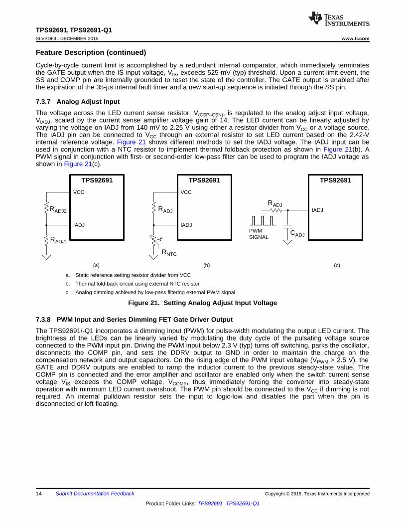
7.3.7 Analog Adjust InputThe voltage across the LED current sense resistor, V(CSP–CSN), is regulated to the analog adjust input voltage,VIADJ, scaled by the current sense amplifier voltage gain of 14. The LED current can be linearly adjusted byvarying the voltage on IADJ from 140 mV to 2.25 V using either a resistor divider from VCC or a voltage source.The IADJ pin can be connected to VCC through an external resistor to set LED current based on the 2.42-Vinternal reference voltage. Figure 21 shows different methods to set the IADJ voltage. The IADJ input can beused in conjunction with a NTC resistor to implement thermal foldback protection as shown in Figure 21(b). APWM signal in conjunction with first- or second-order low-pass filter can be used to program the IADJ voltage asshown in Figure 21(c).
a. Static reference setting resistor divider from VCCb. Thermal fold-back circuit using external NTC resistorc. Analog dimming achieved by low-pass filtering external PWM signal
Figure 21. Setting Analog Adjust Input Voltage
7.3.8 PWM Input and Series Dimming FET Gate Driver OutputThe TPS92691/-Q1 incorporates a dimming input (PWM) for pulse-width modulating the output LED current. Thebrightness of the LEDs can be linearly varied by modulating the duty cycle of the pulsating voltage sourceconnected to the PWM input pin. Driving the PWM input below 2.3 V (typ) turns off switching, parks the oscillator,disconnects the COMP pin, and sets the DDRV output to GND in order to maintain the charge on thecompensation network and output capacitors. On the rising edge of the PWM input voltage (VPWM > 2.5 V), theGATE and DDRV outputs are enabled to ramp the inductor current to the previous steady-state value. TheCOMP pin is connected and the error amplifier and oscillator are enabled only when the switch current sensevoltage VIS exceeds the COMP voltage, VCOMP, thus immediately forcing the converter into steady-stateoperation with minimum LED current overshoot. The PWM pin should be connected to the VCC if dimming is notrequired. An internal pulldown resistor sets the input to logic-low and disables the part when the pin isdisconnected or left floating.
14 Submit Documentation Feedback Copyright © 2015, Texas Instruments Incorporated
Product Folder Links: TPS92691 TPS92691-Q1

+
IMON
TPS92691
PWM
SS
VOCTH
LED+
DDRV
TPS92691
DDRV
TPS92691
LED-
TPS92691, TPS92691-Q1www.ti.com SLVSD68 –DECEMBER 2015
Feature Description (continued)
Figure 22. Series Dimming FET Connections
The DDRV output follows the PWM input signal and is capable of sinking and sourcing up to 500 mA of peakcurrent to control a low-side series connected N-channel dimming FET. Alternatively, the DDRV output can betranslated with an external level-shift circuit to drive a high-side series P-channel dimming FET as shown inFigure 22. The series dimming FET is required to achieve high contrast ratio as it ensures fast rise and fall timesof the LED current in response to the PWM input. Without any dimming FET, the rise and fall times are limited bythe inductor slew rate and the closed-loop bandwidth of the system. Leave the DDRV pin unconnected if notused.
7.3.9 Soft-StartThe soft-start feature helps the regulator gradually reach the steady-state operating point, thus reducing startupstresses and surges. The TPS92691/-Q1 clamps the COMP pin to the SS pin, separated by a diode, until LEDcurrent nears the regulation threshold. The internal 10-µA soft-start current source gradually increases thevoltage on an external soft-start capacitor CSS connected to the SS pin. This results in a gradual rise of theCOMP voltage from GND.
The internal 10-µA current source turns on when VCC exceeds the UVLO threshold. At the beginning of the soft-start sequence, the SS pulldown switch is active and is released when the voltage VSS drops below 25 mV. TheSS pin can also be pulled down by an external switch to stop switching. When the SS pin is externally driven toenable switching, the slew-rate on the COMP pin should be controlled by choosing a compensation capacitorthat avoids large startup transients. The value of CSS should be large enough to charge the output capacitorduring the soft-start transition period.
7.3.10 Current Monitor OutputThe IMON pin voltage represents the LED current measured by the rail-to-rail current sense amplifier across theexternal current shunt resistor. The linear relationship between the IMON voltage and LED current includes theamplifier gain-factor of 14 (see Figure 14). The IMON output can be connected to an external microcontroller orcomparator to facilitate LED open, short, or cable harness fault detection and mitigation based on programmablethreshold VOCTH. The IMON voltage is internally clamped to 3.7 V.
Figure 23. LED Overcurrent Protection using IMON Output
Copyright © 2015, Texas Instruments Incorporated Submit Documentation Feedback 15
Product Folder Links: TPS92691 TPS92691-Q1

TPS92691, TPS92691-Q1SLVSD68 –DECEMBER 2015 www.ti.com
Feature Description (continued)7.3.11 Overvoltage ProtectionThe TPS92691/-Q1 device includes a dedicated OVP pin which can be used for either input or outputovervoltage protection. This pin features a precision 1.24 V (typ) threshold with 20-µA (typ) of hysteresis current.The overvoltage threshold limit is set by a resistor divider network from the input or output terminal to GND.When the OVP pin voltage exceeds the reference threshold, the GATE and DDRV pins are immediately pulledlow and the SS and COMP capacitors are discharged. The GATE is enabled and a new startup sequence isinitiated after the voltage drops below the hysteresis threshold set by the 20-µA source current and the externalresistor divider.
7.3.12 Thermal ProtectionInternal thermal shutdown circuitry is implemented to protect the controller in the event the maximum junctiontemperature is exceeded. When activated, typically at 175°C, the controller is forced into a shutdown mode,disabling the internal regulator. This feature is designed to prevent overheating and damage to the device.
7.4 Device Functional ModesThis device has no additional functional modes.
16 Submit Documentation Feedback Copyright © 2015, Texas Instruments Incorporated
Product Folder Links: TPS92691 TPS92691-Q1

TPS92691-Q1
1
2
3
4
5
6
7
8
16
15
14
13
12
11
10
9
LED+
LEDÅ
VIN
SS
RT/SYNC
PWM
COMP
IADJ
IMON
AGNDPAD
VCC
GATE
IS
PGND
OVP
DDRV
CSP
CSN
VIN
CSS
CCOMP
RT
CIMON
CIN
RIS
Q1
CVCC
ROV1
ROV2
RCS
Q2
D
COUT
COV
CS
L1 L2
RADJ2
RADJ1
VPWM
TPS92691-Q1
1
2
3
4
5
6
7
8
16
15
14
13
12
11
10
9
VIN LED+
LEDÅ
VIN
SS
RT/SYNC
PWM
COMP
IADJ
IMON
AGNDPAD
VCC
GATE
IS
PGND
OVP
DDRV
CSP
CSN
L
ROV1
ROV2
RIS
RCS
Q2
Q1
D
CSS
CCOMP
RT
CIMON
COUT
CVCC
CIN
COV
RADJ2
RADJ1
VPWM
TPS92691, TPS92691-Q1www.ti.com SLVSD68 –DECEMBER 2015
8 Application and Implementation
NOTEInformation in the following applications sections is not part of the TI componentspecification, and TI does not warrant its accuracy or completeness. TI’s customers areresponsible for determining suitability of components for their purposes. Customers shouldvalidate and test their design implementation to confirm system functionality.
8.1 Application InformationThe TPS92691/-Q1 controller is suitable for implementing step-up or step-down LED driver topologies includingBuck, Boost, Buck-Boost, SEPIC, Cuk, and Flyback. Use the following design procedure to select componentvalues for the TPS92691/-Q1 device. This section presents a simplified discussion of the design process for theBuck, Boost, and Buck-Boost converter. The expressions derived for Buck-Boost can also be altered to selectcomponents for a 1:1 coupled-inductor SEPIC converter. The design procedure can be easily adapted forFlyback and Cuk converter topologies.
Figure 24. Boost LED Driver
Figure 25. SEPIC LED Driver
Copyright © 2015, Texas Instruments Incorporated Submit Documentation Feedback 17
Product Folder Links: TPS92691 TPS92691-Q1

TPS92691-Q1
1
2
3
4
5
6
7
8
16
15
14
13
12
11
10
9
VIN LED+
LEDÅ
VIN
SS
RT/SYNC
PWM
COMP
IADJ
IMON
AGNDPAD
VCC
GATE
IS
PGND
OVP
DDRV
CSP
CSN
CSS
CCOMP
RT
CIMON
RADJ2
RADJ1
L
RIS
Q1
CVCC
CIN
ROV1
ROV2
RCS
Q2
COUT
COV
RLS2
RLS1
Q3
D
Q4
VPWM
TPS92691-Q1
1
2
3
4
5
6
7
8
16
15
14
13
12
11
10
9
LED+
LEDÅ
VIN
SS
RT/SYNC
PWM
COMP
IADJ
IMON
AGNDPAD
VCC
GATE
IS
PGND
OVP
DDRV
CSP
CSN
ROV1
ROV2
RCS
Q2
Q1
D
COUT
COV
VIN
CSS
CCOMP
RT
CIMON
CIN RLS2
RLS1
L
RIS
Q1
CVCC
Q3
Q4
RADJ2
RADJ1
VPWM
TPS92691, TPS92691-Q1SLVSD68 –DECEMBER 2015 www.ti.com
Application Information (continued)
Figure 26. Buck-Boost LED Driver
Figure 27. Buck LED Driver
18 Submit Documentation Feedback Copyright © 2015, Texas Instruments Incorporated
Product Folder Links: TPS92691 TPS92691-Q1
2O(MAX) O(MAX)
O(BDRY) SW IN
V VL 1
2 P f V
§ · u �¨ ¸¨ ¸u u © ¹
O(BDRY) LED(MIN) O(MIN)P I Vd u
IN(MIN) MAX
L(PP) SW
V DL
i f
u
' u
LEDL(PP) L
MAX
Ii RR I RR
1 D' � �
�
� �IN(MIN) O MAX
L(PP) SW
V V DL
i f
� u
' u
L(PP) L LEDi RR I RR I' � �
O
IN O
VD
V V
�
O IN
O
V VD
V
�
O
IN
VD
V
TPS92691, TPS92691-Q1www.ti.com SLVSD68 –DECEMBER 2015
Application Information (continued)8.1.1 Duty Cycle ConsiderationsThe switch duty cycle, D, defines the converter operation and is a function of the input and output voltages. Insteady state, the duty cycle is derived using expression:
Buck:
(2)
Boost:
(3)
Buck-Boost:
(4)
The minimum duty cycle, DMIN, and maximum duty cycle, DMAX, are calculated by substituting maximum inputvoltage, VIN(MAX), and the minimum input voltage, VIN(MIN), respectively in the previous expressions. The minimumduty cycle achievable by the device is determined by the leading edge blanking period and the switchingfrequency. The maximum duty cycle is limited by the internal oscillator to 93% (typ) to allow for minimum off-time.It is necessary for the operating duty cycle to be within the operating limits of the device to ensure closed-loopLED current regulation over the specified input and output voltage range.
8.1.2 Inductor SelectionThe inductor peak-to-peak ripple current, ΔiL-PP, is typically set between 10% and 80% of the maximum inductorcurrent, IL, as a good compromise between core loss and copper loss of the inductor. Higher ripple inductorcurrent allows a smaller inductor size, but places more of a burden on the output capacitor to smooth the LEDcurrent ripple. Knowing the desired ripple ratio RR, switching frequency ƒSW, maximum duty cycle DMAX, and thetypical LED current ILED, the inductor value can be calculated as follows:
Buck:
(5)
(6)
Boost and Buck-Boost:
(7)
(8)
As an alternative, the inductor can be selected based on CCM-DCM boundary condition specified based onoutput power, PO(BDRY). The choice of inductor ensures CCM operation in battery-powered LED driverapplications that are designed to support different LED string configurations with a wide range of programmableLED current setpoints. The output power should be calculated based on the lowest LED current and the lowestoutput voltage requirements for a given application.
(9)
Buck:
(10)
Boost:
Copyright © 2015, Texas Instruments Incorporated Submit Documentation Feedback 19
Product Folder Links: TPS92691 TPS92691-Q1

MAXCOUT(RMS) LED
MAX
DI I
1 D u
�
LED(PP)COUT(RMS)
iI
12
'
LED MAXOUT
SW D LED(PP)
I DC
f r i
u
u u '
L(PP)OUT
SW D LED(PP)
iC
8 f r i
'
u u u '
IN(MIN) MAXL(PK) L
SW
V DI I
2 L f
u
�
u u
2
O(BDRY) SWO(MAX) IN
1L
1 12 P f
V V
§ ·
u u u �¨ ¸¨ ¸© ¹
2IN IN
O(BDRY) SW O(MAX)
V VL 1
2 P f V
§ · u �¨ ¸
¨ ¸u u © ¹
TPS92691, TPS92691-Q1SLVSD68 –DECEMBER 2015 www.ti.com
Application Information (continued)
(11)
Buck-Boost:
(12)
The saturation current rating of the inductor should be greater than the peak inductor current, IL(PK), at themaximum operating temperature.
(13)
8.1.3 Output Capacitor SelectionThe output capacitors are required to attenuate the discontinuous or large ripple current generated by switchingand achieve the desired peak-to-peak LED current ripple, ΔiLED(PP). The capacitor value depends on the totalseries resistance of the LED string, rD, the switching frequency, ƒSW, and on the converter topology (that is, step-up or step-down). For the Buck and Cuk topology, the inductor is in series with LED load and requires a smallercapacitor than the Boost, Buck-Boost, and SEPIC topologies to achieve the same LED ripple current. Thecapacitance required for the target LED ripple current can be calculated based on following equations.
Buck:
(14)
Boost and Buck-Boost:
(15)
When choosing the output capacitors, it is important to consider the ESR and the ESL characteristics as theydirectly impact the LED current ripple. Ceramic capacitors are the best choice due to their low ESR, high ripplecurrent rating, long lifetime, and good temperature performance. When selecting ceramic capacitors, it isimportant to consider the derating factors associated with higher temperature and DC bias operating conditions.TI recommends an X7R dielectric with voltage rating greater than maximum LED stack voltage. An aluminumelectrolytic capacitor can be used in parallel with ceramic capacitors to provide bulk energy storage. Thealuminum capacitors must have necessary RMS current and temperature ratings to ensure prolonged operatinglifetime. The minimum allowable RMS output capacitor current rating, ICOUT(RMS), can be approximated:
Buck:
(16)
Boost and Buck-Boost:
(17)
The expressions (Equation 14 to Equation 17) are best suited for designs driving a fixed LED load, with knownoutput voltage and LED current. For applications that are required to support different LED string configurationswith a wide range of programmable LED current setpoints, the previous expressions are rearranged to reflectoutput capacitance based on the maximum output power, PO(MAX), to ensure that LED current ripplespecifications are met over the entire range of operation. Typical Buck-Boost LED Driver provides the details forBuck-Boost LED driver.
20 Submit Documentation Feedback Copyright © 2015, Texas Instruments Incorporated
Product Folder Links: TPS92691 TPS92691-Q1

DS O(OV)V V 1.2 u
Q(RMS) LED MAXI I D u
DS IN(MAX)V V 1.2 u
VIN
TPS92691
VINC
VINR
LED MAXIN
SW IN(PP)
I DC
f v
u
u '
L(PP)IN
SW IN(PP)
iC
8 f v
'
u u '
LED MAX MAXIN
SW IN(PP)
I D (1 D )C
f v
u u �
u '
TPS92691, TPS92691-Q1www.ti.com SLVSD68 –DECEMBER 2015
Application Information (continued)8.1.4 Input Capacitor SelectionThe input capacitors, CIN, smooth the input voltage ripple and store energy to supply input current during inputvoltage or PWM dimming transients. The series inductor in the Boost, SEPIC, and Cuk topology providescontinuous input current and requires a smaller input capacitor to achieve desired input ripple voltage, ΔvIN(PP).The Buck and Buck-Boost topology have discontinuous input current and require a larger capacitor to achievethe same input voltage ripple. Based on the switching frequency, ƒSW, and the maximum duty cycle, DMAX, theinput capacitor value can be calculated as follows:
Buck:
(18)
Boost:
(19)
Buck-Boost:
(20)
X7R dielectric-based ceramic capacitors are the best choice due to their low ESR, high ripple current rating, andgood temperature performance. For applications using PWM dimming, TI recommends an aluminum electrolyticcapacitor in addition to ceramic capacitors to minimize the voltage deviation due to large input current transientsgenerated in conjunction with the rising and falling edges of the LED current.
Figure 28. VIN Filter
For most applications, TI highly recommends to bypass the VIN pin with a 0.1-µF ceramic capacitor placed asclose as possible to the device and add a series 10-Ω resistor to create a 150-kHz low-pass filter and eliminateundesired high-frequency noise.
8.1.5 Main Power MOSFET SelectionThe power MOSFET should be able to sustain the maximum switch node voltage, VSW, and switch RMS currentderived based on the converter topology. TI recommends a drain voltage VDS rating of at least 20% greater thanthe maximum switch node voltage to ensure safe operation. The MOSFET drain-to-source breakdown voltage,VDS, and RMS current ratings are calculated using the following expressions.
Buck:
(21)
(22)
Boost:
(23)
Copyright © 2015, Texas Instruments Incorporated Submit Documentation Feedback 21
Product Folder Links: TPS92691 TPS92691-Q1
IADJLED
CS
VI
14 R
u
LEDCS
0.172I
R
D L M A XI I (1 D ) u �
2L SW RSS SW
SWGATE
I V C fP
I
u u u
2COND DS Q(RMS)P R I u
MAXQ(RMS) LED
MAX
DI I
1 D u
�
� �DS IN(MAX) O(OV)V V V 1.2 � u
MAXQ(RMS) LED
MAX
DI I
1 D u
�
TPS92691, TPS92691-Q1SLVSD68 –DECEMBER 2015 www.ti.com
Application Information (continued)
(24)
Buck-Boost:
(25)
(26)
Where the voltage, VO(OV), is the overvoltage protection threshold and the worst-case output voltage under faultconditions.
Select a MOSFET with low total gate charge, Qg, to minimize gate drive and switching losses. The MOSFET RDSresistance is usually a less critical parameter because the switch conduction losses are not a significant part ofthe total converter losses at high operating frequencies. The switching and conduction losses are calculated asfollows:
(27)
(28)
CRSS is the MOSFET reverse transfer capacitance. IL is the average inductor current. IGATE is gate drive outputcurrent, typically 500 mA. The MOSFET power rating and package should be selected based on the totalcalculated loss, the ambient operating temperature, and maximum allowable temperature rise.
8.1.6 Rectifier Diode SelectionA Schottky diode (when used as a rectifier) provides the best efficiency due to low forward voltage drop andnear-zero reverse recovery time. TI recommends a diode with a reverse breakdown voltage, VD(BR), greater thanor equal to MOSFET drain-to-source voltage, VDS, for reliable performance. It is important to understand theleakage current characteristics of the Schottky diode, especially at high operating temperatures because itimpacts the overall converter operation and efficiency.
The current through the diode, ID, is given by:(29)
The diode should be sized to exceed the current rating, and the package should be able to dissipate powerwithout exceeding the maximum allowable temperature.
8.1.7 LED Current ProgrammingThe LED current is set by the external current sense resistor, RCS, and the analog adjust voltage, VIADJ. Thecurrent sense resistor is placed in series with the LED load and can be located either on the high side(connected to the output, VO), or on the low side (connected to ground, GND). The CSP and CSN inputs of theinternal rail-to-rail current sense amplifier are connected to the RCS resistor to enable closed-loop regulation.When VIADJ > 2.5 V, the internal 2.42-V reference sets the V(CSP-CSN) threshold to 172 mV and the LED current isregulated to:
(30)
The LED current can be programmed by varying VIADJ between 140 mV to 2.25 V. The LED current can becalculated using:
(31)
22 Submit Documentation Feedback Copyright © 2015, Texas Instruments Incorporated
Product Folder Links: TPS92691 TPS92691-Q1

ZLED0
COMP
P
s1
ÖiG
Öv s1
§ ·�¨ ¸Z© ¹
§ ·�¨ ¸Z© ¹
VCC
GATE
IS
PGND
TPS92691
ISR100 O
1 nF
IS(LIMIT) SL MAXIS
L(PK)
V V DR
I
� u
SL SWIS
O(MAX)
2 V L fR
V
u u u
TPS92691, TPS92691-Q1www.ti.com SLVSD68 –DECEMBER 2015
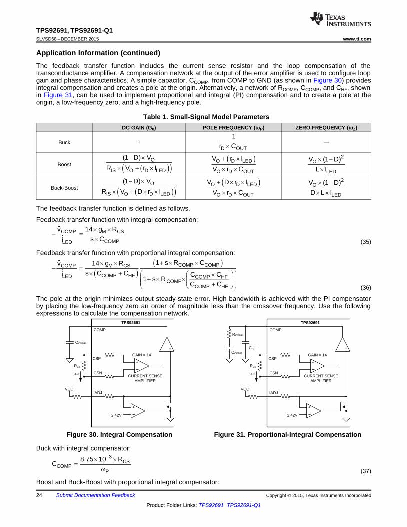
Application Information (continued)The output voltage ripple should be limited to 50 mV for best performance. TI recommends a low-pass common-mode filter consisting of 10-Ω resistors is series with CSP and CSN inputs and 0.01-µF capacitors to ground tominimize the impact of voltage ripple and noise on LED current accuracy (see Figure 20). A 0.1-µF capacitoracross CSP and CSN is included to filter high-frequency differential noise.
8.1.8 Switch Current Sense Resistor and Slope CompensationThe switch current sense resistor, RIS, is used to implement peak current mode control and to set the peakswitch current limit. The value of switch current sense RIS is selected to achieve stable inner current loopoperation based on the magnitude of slope compensation ramp, VSL, and to protect the main switching MOSFETunder fault conditions. The lower of the two values calculated using the following equations should be selectedfor RIS.
(32)
(33)
The internal slope compensation voltage, VSL is fixed at 200 mV (typ). A resistor can be placed in series with theIS pin to increase slope compensation, if necessary. The peak switch current limit is set based on the internalcurrent limit threshold of 525 mV (typ) and adjusted based on slope compensation to ensure reliable operationwhile PWM dimming.
Figure 29. IS Input Filter
The use of a 1-nF and 100-Ω low-pass filter is optional. If used, the resistor value should be less than 500 Ω tolimit its influence on the internal slope compensation signal.
8.1.9 Feedback CompensationThe open-loop response is the product of the modulator transfer function (shown in Equation 34) and thefeedback transfer function. Using a first-order approximation, the modulator transfer function can be modeled asa single pole created by the output capacitor, and in the boost and buck-boost topologies, a right half-plane zerocreated by the inductor, where both have a dependence on the LED string dynamic resistance, rD. Because TIrecommends a ceramic capacitor, the ESR of the output capacitor is neglected in the analysis. The small-signalmodulator model also includes a DC gain factor that is dependent on the duty cycle, output voltage, and LEDcurrent.
(34)
Table 1 summarizes the expression for the small-signal model parameters.
Copyright © 2015, Texas Instruments Incorporated Submit Documentation Feedback 23
Product Folder Links: TPS92691 TPS92691-Q1
3CS
COMPP
8.75 10 RC
�u u
Z
+
+
COMP
CSP
CSN
IADJ
+
CURRENT SENSE AMPLIFIER
GAIN = 14
RCS
ILED
VCC
2.42V
CCOMP
TPS92691
+
+
COMP
CSP
CSN
IADJ
+
CURRENT SENSE AMPLIFIER
GAIN = 14
RCS
ILED
VCC
2.42V
CHF
TPS92691
CCOMP
RCOMP
� �� �COMP COMPCOMP M CS
COMP HFLED COMP HFCOMP
COMP HF
Ö 1 s R Cv 14 g RÖ s C Ci C C
1 s RC C
� u uu u�
u � § ·§ ·u� u u¨ ¸¨ ¸¨ ¸�© ¹© ¹
COMP M CS
COMPLED
Öv 14 g RÖ s Ci
u u�
u
� �� �O
IS O D LED
(1 D) V
R V D r I
� u
u � u u
� �O D LED
O D OUT
V D r I
V r C
� u u
u u
2O
LED
V (1 D)
D L I
u �
u u
� �� �O
IS O D LED
(1 D) V
R V r I
� u
u � u
� �O D LED
O D OUT
V r I
V r C
� u
u u
2O
LED
V (1 D)
L I
u �
u
D OUT
1r Cu
TPS92691, TPS92691-Q1SLVSD68 –DECEMBER 2015 www.ti.com
Application Information (continued)The feedback transfer function includes the current sense resistor and the loop compensation of thetransconductance amplifier. A compensation network at the output of the error amplifier is used to configure loopgain and phase characteristics. A simple capacitor, CCOMP, from COMP to GND (as shown in Figure 30) providesintegral compensation and creates a pole at the origin. Alternatively, a network of RCOMP, CCOMP, and CHF, shownin Figure 31, can be used to implement proportional and integral (PI) compensation and to create a pole at theorigin, a low-frequency zero, and a high-frequency pole.
Table 1. Small-Signal Model ParametersDC GAIN (G0) POLE FREQUENCY (ωP) ZERO FREQUENCY (ωZ)
Buck 1 —
Boost
Buck-Boost
The feedback transfer function is defined as follows.
Feedback transfer function with integral compensation:
(35)
Feedback transfer function with proportional integral compensation:
(36)
The pole at the origin minimizes output steady-state error. High bandwidth is achieved with the PI compensatorby placing the low-frequency zero an order of magnitude less than the crossover frequency. Use the followingexpressions to calculate the compensation network.
Figure 30. Integral Compensation Figure 31. Proportional-Integral Compensation
Buck with integral compensator:
(37)
Boost and Buck-Boost with proportional integral compensator:
24 Submit Documentation Feedback Copyright © 2015, Texas Instruments Incorporated
Product Folder Links: TPS92691 TPS92691-Q1
OV(HYS) OVP(HYS) OV2V I R u
OV2O(OV) OVP(THR)
OV1
RV V 0.7
R u �
OV1 OV2O(OV) OVP(THR)
OV1
R RV V
R
§ ·� u ¨ ¸
© ¹
6 OUT OUTSS SS
LED
C VC 12.5 10 t
I� § ·u
u �¨ ¸© ¹
COMPP COMP
1R
C Z u
COMPHF
CC
100
3 CS 0COMP
Z
R GC 8.75 10� § ·u
u u ¨ ¸Z© ¹
TPS92691, TPS92691-Q1www.ti.com SLVSD68 –DECEMBER 2015
(38)
(39)
(40)
The loop response is verified by applying step input voltage transients. The goal is to minimize LED currentovershoot and undershoot with a damped response. Additional tuning of the compensation network may benecessary to optimize PWM dimming performance.
8.1.10 Soft-StartThe soft-start time (tSS) is the time required for the LED current to reach the target setpoint. The required soft-start time, tSS, is programmed using a capacitor, CSS, from SS pin to GND, and is based on the LED current,output capacitor, and output voltage.
(41)
8.1.11 Overvoltage ProtectionThe overvoltage threshold is programmed using a resistor divider, ROV2 and ROV1, from the output voltage, VO, toground for Boost and SEPIC topologies, as shown in Figure 24 and Figure 25. If the LEDs are referenced to apotential other than ground, as in the Buck-Boost or Buck configuration, the output voltage is sensed andtranslated to ground by using a PNP transistor and level-shift resistors, as shown in Figure 27 and Figure 26.The overvoltage turn-off threshold, VO(OV), is:
Boost:
(42)
Buck and Buck-Boost:
(43)
The overvoltage hysteresis, VOV(HYS) is:
(44)
8.1.12 PWM Dimming ConsiderationsWhen PWM dimming, the TPS92691/-Q1 requires another MOSFET placed in series with the LED load. ThisMOSFET should have a voltage rating greater than the output voltage, VO, and a current rating at least 10%higher than the nominal LED current, ILED.
It is important to control the slew-rate of the external FET to achieve a damped LED current response to PWMrising-edge transitions. For a low-side, N-channel dimming FET, the slew-rate is controlled by placing a resistorin series with the GATE pin. The rise and fall times depend on the value of the resistor and the gate-to-sourcecapacitance of the MOSFET. The series resistor can be bypassed with a diode for fast rise time and slow falltimes to achieve 100:1 or higher contrast ratios. If a high-side P-channel dimming FET is used, the rise and falltimes can be controlled by selecting appropriate resistors for the level-shift network, RLS1 and RLS2, as shown inFigure 26.
Copyright © 2015, Texas Instruments Incorporated Submit Documentation Feedback 25
Product Folder Links: TPS92691 TPS92691-Q1
TPS92691, TPS92691-Q1SLVSD68 –DECEMBER 2015 www.ti.com
8.2 Typical Applications
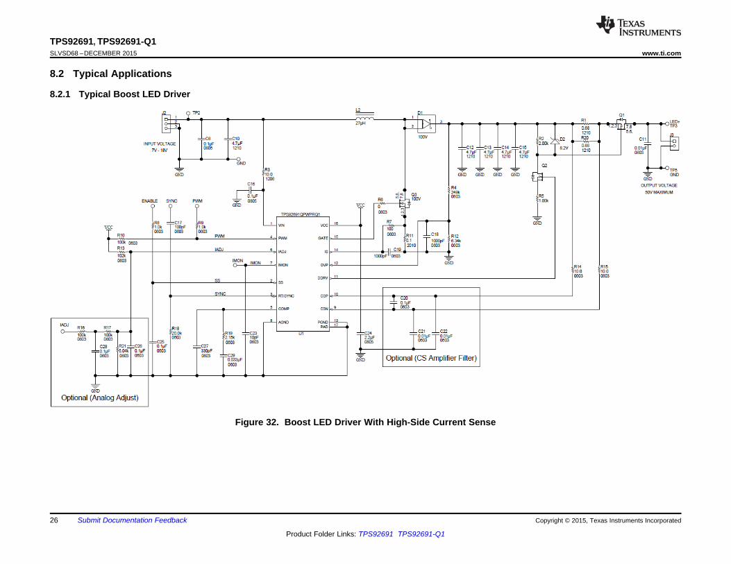
8.2.1 Typical Boost LED Driver
Figure 32. Boost LED Driver With High-Side Current Sense
26 Submit Documentation Feedback Copyright © 2015, Texas Instruments Incorporated
Product Folder Links: TPS92691 TPS92691-Q1
� � � �
10 103
T 1.047 1.0473SW
1.432 10 1.432 10R 20.05 10
f 390 10
u u u
u
O IN(MAX)MIN
O
V V 38.4 18D 0.5312
V 38.4
� �
O IN(MIN)MAX
O
V V 38.4 7D 0.8177
V 38.4
� �
O IN
O
V V 38.4 14D 0.6354
V 38.4
� �
TPS92691, TPS92691-Q1www.ti.com SLVSD68 –DECEMBER 2015
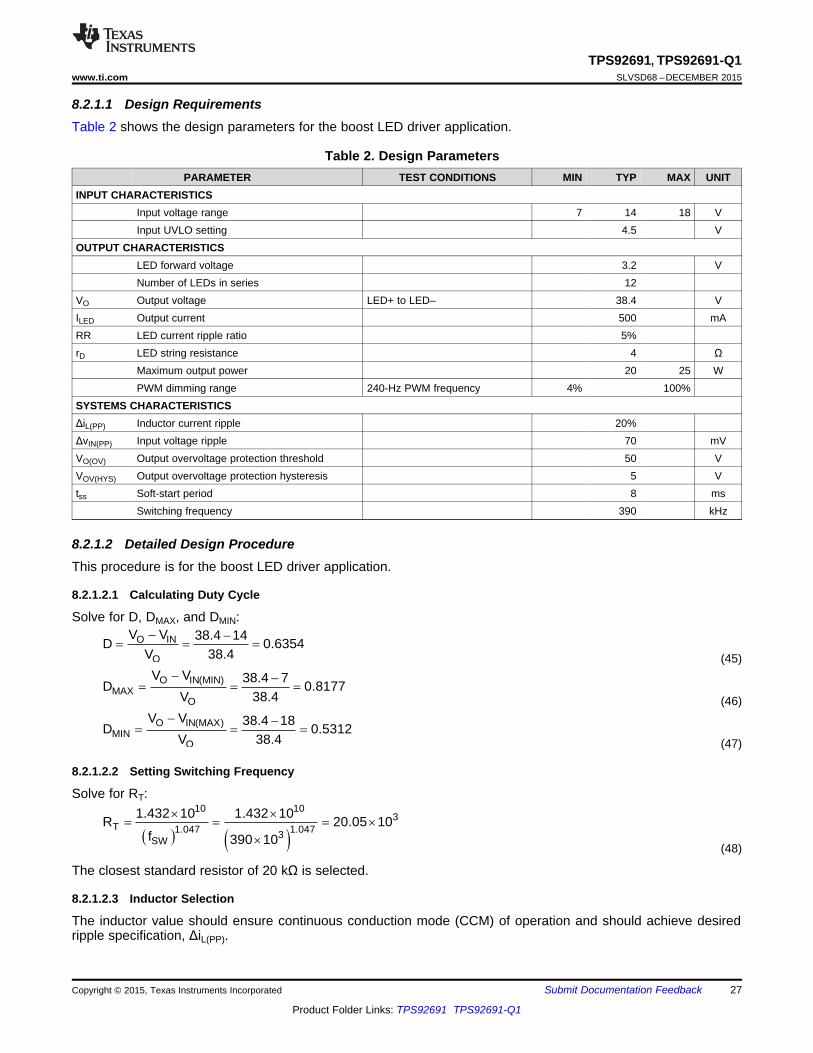
8.2.1.1 Design RequirementsTable 2 shows the design parameters for the boost LED driver application.
Table 2. Design ParametersPARAMETER TEST CONDITIONS MIN TYP MAX UNIT
INPUT CHARACTERISTICSInput voltage range 7 14 18 VInput UVLO setting 4.5 V
OUTPUT CHARACTERISTICSLED forward voltage 3.2 VNumber of LEDs in series 12
VO Output voltage LED+ to LED– 38.4 VILED Output current 500 mARR LED current ripple ratio 5%rD LED string resistance 4 Ω
Maximum output power 20 25 WPWM dimming range 240-Hz PWM frequency 4% 100%
SYSTEMS CHARACTERISTICSΔiL(PP) Inductor current ripple 20%ΔvIN(PP) Input voltage ripple 70 mVVO(OV) Output overvoltage protection threshold 50 VVOV(HYS) Output overvoltage protection hysteresis 5 Vtss Soft-start period 8 ms
Switching frequency 390 kHz
8.2.1.2 Detailed Design ProcedureThis procedure is for the boost LED driver application.
8.2.1.2.1 Calculating Duty Cycle
Solve for D, DMAX, and DMIN:
(45)
(46)
(47)
8.2.1.2.2 Setting Switching Frequency
Solve for RT:
(48)
The closest standard resistor of 20 kΩ is selected.
8.2.1.2.3 Inductor Selection
The inductor value should ensure continuous conduction mode (CCM) of operation and should achieve desiredripple specification, ΔiL(PP).
Copyright © 2015, Texas Instruments Incorporated Submit Documentation Feedback 27
Product Folder Links: TPS92691 TPS92691-Q1

D L MAX LEDI I (1 D ) I 0.5 u �
D(BR) O(OV)V V 1.2 50 1.2 60 u u
MAXQ(RMS) LED
MAX
D 0.8177I I 0.5 2.48
1 D 1 0.8177 u u
� �
DS O(OV)V V 1.2 50 1.2 60 u u
L(PP) 6IN 3 3
SW IN(PP)
i 0.5436C 2.49 10
8 f v 8 390 10 70 10�
�
' u
u u ' u u u u
6LED MAXOUT 3 3
SW D LED(PP)
I D 0.5 0.8177C 10.48 10
f r i 390 10 4 25 10�
�
u u u
u u' u u u u
3LED(PP) LEDi 0.05 I 25 10�
' u u
IN(MIN) MAXLEDL(PK) 6 3
MAX SW
V DI 0.5 7 0.8177I 3.01
1 D 2 L f 1 0.8177 2 27 10 390 10�
u u � �
� u u � u u u u
IN(MIN) MAXL(PP) 6 3
SW
V D 7 0.8177i 0.5436
L f 27 10 390 10�
u u'
u u u u
IN(MIN) MAX 63
L(PP) SW
V D 7 0.8177L 26.76 10
i f 0.5485 390 10�
u u u
' u u u
LEDL(PP)
MAX
I 0.5i RR 0.2 0.5485
1 D 1 0.8177' u u
� �
TPS92691, TPS92691-Q1SLVSD68 –DECEMBER 2015 www.ti.com
(49)
Solving for inductor:
(50)
The closest standard inductor is 27 µH. The expected inductor ripple based on the chosen inductor is:
(51)
The inductor saturation current rating should be greater than the peak inductor current, IL(PK).
(52)
8.2.1.2.4 Output Capacitor Selection
The specified peak-to-peak LED current ripple, ΔiLED(PP), is:
(53)
The output capacitance required to achieve the target LED current ripple is:
(54)
Considering 40% derating factor under DC bias operation, four 4.7-µF, 100-V rated X7R ceramic capacitors areused in parallel to achieve a combined output capacitance of 18.8 µF.
8.2.1.2.5 Input Capacitor Selection
The input capacitor is required to reduce switching noise conducted through the input wires and reduced theinput impedance of the LED driver. The capacitor required to limit peak-to-peak input ripple voltage ripple,ΔvIN(PP), to 70 mV is given by:
(55)
A 4.7-µF, 50-V X7R ceramic capacitor is selected.
8.2.1.2.6 Main N-Channel MOSFET Selection
The MOSFET ratings should exceed the maximum output voltage and RMS switch current given by:
(56)
(57)
A 60-V or a 100-V N-channel MOSFET with current rating exceeding 3 A is required for this design.
8.2.1.2.7 Rectifying Diode Selection
The diode should be selected based on the following voltage and current ratings:
(58)
(59)
A 60-V or a 100-V Schottky diode with low reverse leakage current is suitable for this design. The package mustbe able to handle the power dissipation resulting from continuous forward current, ID, of 0.5 A.
28 Submit Documentation Feedback Copyright © 2015, Texas Instruments Incorporated
Product Folder Links: TPS92691 TPS92691-Q1
OV(HYS) 3OV2 6 6
V 5R 250 10
20 10 20 10� � u
u u
66 6 3 9OUT OUT
SS SSLED
C V 18.8 10 38.4C 12.5 10 t 12.5 10 8 10 81.9 10
I 0.5
�� � � �
§ ·§ ·u u u u � u u � u¨ ¸¨ ¸ ¨ ¸
© ¹ © ¹
3COMP 3 9
P COMP
1 1R 2.165 10
C 14 10 33 10� uZ u u u u
3 3 9CS 0COMP 3
Z
R G 0.34 3.466C 8.75 10 8.75 10 27.27 10
378.12 10� � �§ ·u u§ ·
u u u u u¨ ¸ ¨ ¸Z u© ¹© ¹
3ZLED
0COMP
3P
s s1 1Öi 378.12 10G 3.466Öv ss 11
14 10
§ · § ·� �¨ ¸ ¨ ¸Z u© ¹ © ¹ § · § ·
��¨ ¸ ¨ ¸Z u© ¹© ¹
IS(LIMIT) SL MAXIS
L(PK)
V V D 0.525 0.2 0.8177R 0.12
I 3.01
� u � u
6 3SL SW
ISO(MAX)
2 V L f 2 0.2 27 10 390 10R 0.11
V 38.4
�u u u u u u u u
CSLED
0.172 0.172R 0.344
I 0.5
TPS92691, TPS92691-Q1www.ti.com SLVSD68 –DECEMBER 2015
8.2.1.2.8 Programming LED Current
LED current is based on the current shunt resistor, RCS and the V(CSP-CSN) threshold set by the voltage on theIADJ pin VIADJ. By default, IADJ is tied to VCC via an external resistor to enable the internal reference voltage of2.42 V that then sets the V(CSP-CSN) threshold to 172 mV. The current shunt resistor value is calculated by:
(60)
Two 0.68-Ω resistors are connected in parallel to achieve RCS of 0.34 Ω.
8.2.1.2.9 Setting Switch Current Limit and Slope Compensation
The switch current sense resistor, RIS, is calculated by solving the following equations and choosing the lowestvalue:
(61)
(62)
A standard value of 0.1 Ω is selected.
8.2.1.2.10 Deriving Compensator Parameters
The modulator transfer function for the Boost converter is derived for nominal VIN voltage and corresponding dutycycle, D, and is given by the following equation. (See Table 1 for more information.)
(63)
The proportional-integral compensator components CCOMP and RCOMP are obtained by solving the followingexpressions:
(64)
(65)
The closet standard capacitor of 33 nF and resistor of 2.15 kΩ is selected. The high frequency pole location isset by a 100 pF CHF capacitor.
8.2.1.2.11 Setting Start-up Duration
The soft-start capacitor required to achieve start-up in 8 ms is given by:
(66)
The closet standard capacitor of 100 nF is selected.
8.2.1.2.12 Setting Overvoltage Protection Threshold
The overvoltage protection threshold of 50 V and hysteresis of 5 V is set by the ROV1 and ROV2 resistor divider.
(67)
Copyright © 2015, Texas Instruments Incorporated Submit Documentation Feedback 29
Product Folder Links: TPS92691 TPS92691-Q1
VIN (V)
Effi
cien
cy (
%)
7 8 9 10 11 12 13 14 15 16 17 1875
80
85
90
95
100
D021
3 3OV1 OV2
O(OV)
1.24 1.24R R 250 10 6.36 10
V 1.24 50 1.24
§ · § · u u¨ ¸ ¨ ¸¨ ¸� �© ¹© ¹
TPS92691, TPS92691-Q1SLVSD68 –DECEMBER 2015 www.ti.com
(68)
The standard resistor values of 249 kΩ and 6.34 kΩ are chosen.
8.2.1.2.13 PWM Dimming Considerations
A series dimming FET is required to meet PWM dimming specification from 100% to 4% duty cycle. A 60-V, 2-AN-channel FET is suitable for this application.
As an alternative, a 60-V, 2-A P-channel FET could be used to achieve PWM dimming. An external level-shiftcircuit is required to translate the DDRV signal to the gate of the P-channel dimming FET. The drive strength of 5mA and gate-source voltage of 15 V are set by the 1-kΩ and 2-kΩ level-translator resistors and a small-signal N-channel MOSFET, whose gate is connected to DDRV.
By default, the PWM pin is connected to VCC through a 100-kΩ resistor to enable the part upon start-up.
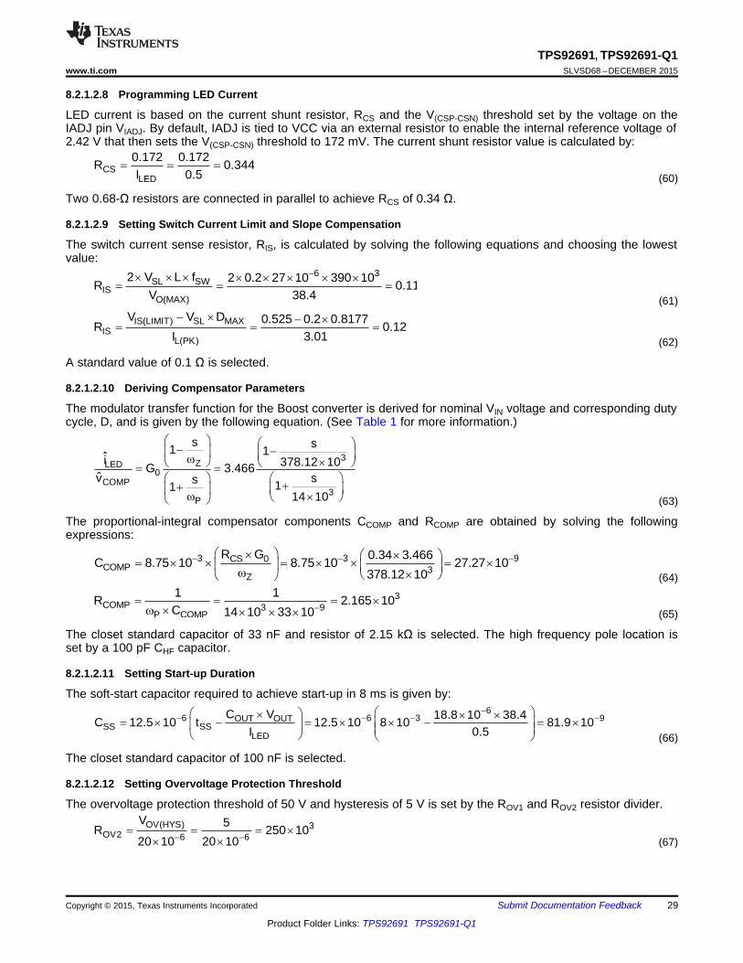
8.2.1.3 Application CurvesThese curves are for the boost LED driver.
Ch1: Switch node voltage;Ch3: Switch sense current resistor voltage;Ch4: LED current; Time: 1 µs/div
Figure 34. Normal OperationFigure 33. Efficiency vs Input Voltage
Ch1: Input voltage; Ch2: Soft-start (SS) voltage; Ch1: Output voltage;Ch3: Input current; Ch2: Soft-start (SS) voltage;Ch4: LED current; Time: 2 ms/div Ch4: LED current; Time: 200 ms/div
Figure 35. Startup Transient Figure 36. Overvoltage Protection
30 Submit Documentation Feedback Copyright © 2015, Texas Instruments Incorporated
Product Folder Links: TPS92691 TPS92691-Q1

TPS92691, TPS92691-Q1www.ti.com SLVSD68 –DECEMBER 2015
Ch1: GATE voltage; Ch2: External CLK signal; Ch1: DDRV voltage; Ch2: PWM input;Ch3: Switch sense current resistor voltage; Ch3: Switch sense current resistor voltage;Ch4: LED current; Time: 1 µs/div Ch4: LED current; Time: 2 ms/div
Figure 37. Clock Synchronization Figure 38. PWM Dimming Transient
Ch1: DDRV voltage; Ch2: PWM input; Ch1: Input voltage;Ch3: Switch sense current resistor voltage; Ch2: IMON voltage;Ch4: LED current; Time: 4 µs/div Ch4: LED current; Time: 2 ms/div
Figure 39. PWM Dimming Transient (Zoomed) Figure 40. Step Input Voltage Transient and IMONBehavior
Copyright © 2015, Texas Instruments Incorporated Submit Documentation Feedback 31
Product Folder Links: TPS92691 TPS92691-Q1

TPS92691, TPS92691-Q1SLVSD68 –DECEMBER 2015 www.ti.com
8.2.2 Typical Buck-Boost LED Driver
Figure 41. Buck-Boost LED Driver
32 Submit Documentation Feedback Copyright © 2015, Texas Instruments Incorporated
Product Folder Links: TPS92691 TPS92691-Q1
O(MIN)MIN
O(MIN) IN(MAX)
V 9.6D 0.3478
V V 9.6 18
� �
O(MAX)MAX
O(MAX) IN(MIN)
V 28.8D 0.8045
V V 28.8 7
� �
O
O IN
V 19.2D 0.5783
V V 19.2 14
� �
TPS92691, TPS92691-Q1www.ti.com SLVSD68 –DECEMBER 2015
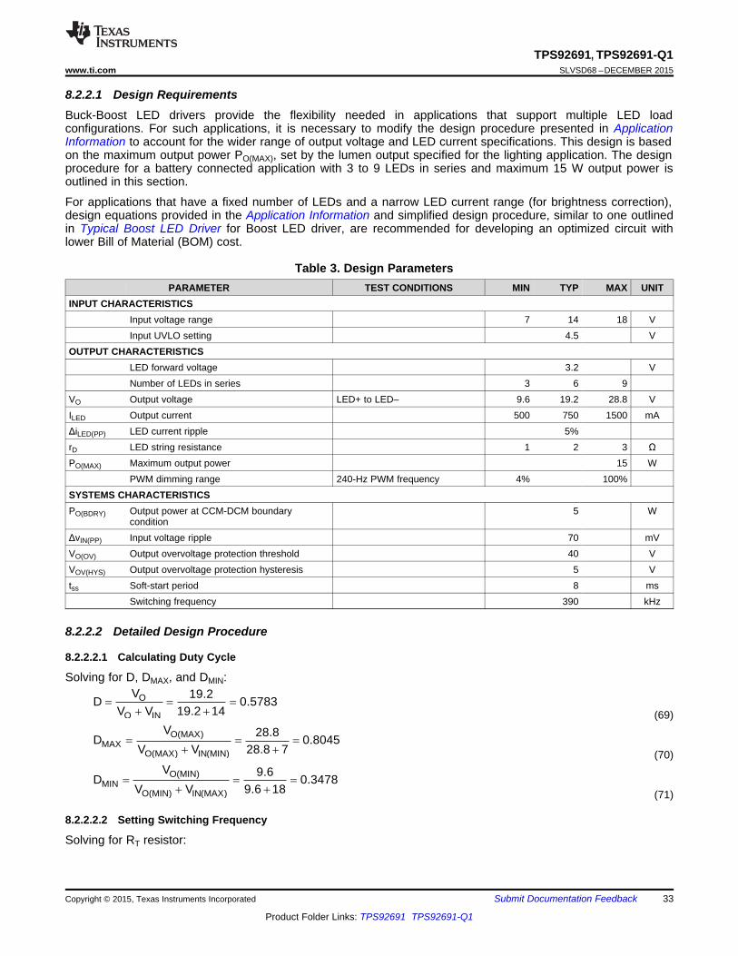
8.2.2.1 Design RequirementsBuck-Boost LED drivers provide the flexibility needed in applications that support multiple LED loadconfigurations. For such applications, it is necessary to modify the design procedure presented in ApplicationInformation to account for the wider range of output voltage and LED current specifications. This design is basedon the maximum output power PO(MAX), set by the lumen output specified for the lighting application. The designprocedure for a battery connected application with 3 to 9 LEDs in series and maximum 15 W output power isoutlined in this section.
For applications that have a fixed number of LEDs and a narrow LED current range (for brightness correction),design equations provided in the Application Information and simplified design procedure, similar to one outlinedin Typical Boost LED Driver for Boost LED driver, are recommended for developing an optimized circuit withlower Bill of Material (BOM) cost.
Table 3. Design ParametersPARAMETER TEST CONDITIONS MIN TYP MAX UNIT
INPUT CHARACTERISTICSInput voltage range 7 14 18 VInput UVLO setting 4.5 V
OUTPUT CHARACTERISTICSLED forward voltage 3.2 VNumber of LEDs in series 3 6 9
VO Output voltage LED+ to LED– 9.6 19.2 28.8 VILED Output current 500 750 1500 mAΔiLED(PP) LED current ripple 5%rD LED string resistance 1 2 3 ΩPO(MAX) Maximum output power 15 W
PWM dimming range 240-Hz PWM frequency 4% 100%SYSTEMS CHARACTERISTICSPO(BDRY) Output power at CCM-DCM boundary 5 W
conditionΔvIN(PP) Input voltage ripple 70 mVVO(OV) Output overvoltage protection threshold 40 VVOV(HYS) Output overvoltage protection hysteresis 5 Vtss Soft-start period 8 ms
Switching frequency 390 kHz
8.2.2.2 Detailed Design Procedure
8.2.2.2.1 Calculating Duty Cycle
Solving for D, DMAX, and DMIN:
(69)
(70)
(71)
8.2.2.2.2 Setting Switching Frequency
Solving for RT resistor:
Copyright © 2015, Texas Instruments Incorporated Submit Documentation Feedback 33
Product Folder Links: TPS92691 TPS92691-Q1

� �DS O(OV) IN(MAX)V 1.2 V V 1.2 (40 18) 69.6 u � u �
� � � �O(MAX) 6
IN 3SW IN(PP) O(MIN) IN(MIN)
P 15C 33.1 10
f v V V 390 10 0.07 9.6 7� u
u' u � u u u �
� �6
OUT 3
15C 30.9 10
390 10 1 0.075 9.6 7� u
u u u u �
� �O(MAX)
OUTSW D(MIN) LED(PP) O(MIN) IN(MIN)
PC
f r i V V
u u' u �
� �L(PK) 6 3
1 1 9.6 7I 15 3.863
9.6 7 2 33 10 390 10 9.6 7�
u§ · u � � ¨ ¸
u u u u u �© ¹
� �O(MIN) IN(MIN)
L(PK) O(MAX)O(MIN) IN(MIN) SW O(MIN) IN(MIN)
V V1 1I P
V V 2 L f V V
§ · u u � �¨ ¸
¨ ¸ u u u �© ¹
IN(MIN) MAXL(PP) 6 3
SW
V D 7 0.8045i 0.4376
L f 33 10 390 10�
u u'
u u u u
62 2
3O(BDRY) SW
O(MAX) IN(MAX)
1 1L 31.46 10
1 11 1 2 5 390 102 P f 28.8 18V V
� u§ · § ·
u u u u �u u u � ¨ ¸¨ ¸¨ ¸ © ¹© ¹
� � � �
10 103
T 1.047 1.0473SW
1.432 10 1.432 10R 20.05 10
f 390 10
u u u
u
TPS92691, TPS92691-Q1SLVSD68 –DECEMBER 2015 www.ti.com
(72)
8.2.2.2.3 Inductor Selection
The inductor is selected to meet the CCM-DCM boundary power requirement, PO(BDRY). Typically, the boundarycondition is set to enable CCM operation at the lowest possible operating power based on minimum LED forwardvoltage drop and LED current. In most applications, PO(BDRY) is set to be 1/3 of the maximum output power,PO(MAX). The inductor value is calculated for maximum input voltage, VIN(MAX), and output voltage, VO(MAX):
(73)
The closest standard value of 33 µH is selected. The inductor ripple current is given by:
(74)
The inductor saturation rating should exceed the calculated peak current which is based on the maximum outputpower using the following expression:
(75)
8.2.2.2.4 Output Capacitor Selection
The output capacitor should be selected to achieve the 5% peak-to-peak LED current ripple specification. Basedon the maximum power, the capacitor is calculated as follows:
(76)
A minimum of four 10-µF, 50-V X7R ceramic capacitors in parallel are needed to meet the LED current ripplespecification over the entire range of output power. Additional capacitance may be required based on thederating factor under DC bias operation.
8.2.2.2.5 Input Capacitor Selection
The input capacitor is calculated based on the peak-to-peak input ripple specifications, ΔvIN(PP). The capacitorrequired to limit the ripple to 70 mV over range of operation is calculated using:
(77)
A parallel combination of four 10-µF, 50-V X7R ceramic capacitors are used for a combined capacitance of 40µF. Additional capacitance may be required based on the derating factor under DC bias operation.
8.2.2.2.6 Main N-Channel MOSFET Selection
Calculating the minimum transistor voltage and current rating:
(78)
34 Submit Documentation Feedback Copyright © 2015, Texas Instruments Incorporated
Product Folder Links: TPS92691 TPS92691-Q1

3ZLED
0COMP
3P
s s1 1Öi 82.92 10G 1.876Öv ss 11
8.68 10
§ · § ·� �¨ ¸ ¨ ¸Z u© ¹ © ¹ § · § ·
��¨ ¸ ¨ ¸Z u© ¹© ¹
IADJCS
LED(MAX)
V 2.1R 0.1
14 I 14 1.5
u u
IS(LIMIT) SL MAXIS
L(PK)
V V D 0.525 0.2 0.8045R 0.094
I 3.863
� u � u
6 3SL SW
ISO(MAX)
2 V L f 2 0.2 33 10 390 10R 0.179
V 28.8
�u u u u u u u u
D LED(MAX)I I 1.5
� �D(BR) O(OV) IN(MAX)V 1.2 V V 1.2 (40 18) 69.6 u � u �
O(MAX) IN(MIN)Q(RMS)
IN(MIN) O(MIN)
P V 15 7I 1 1 2.82
V V 7 9.6
§ · § · � � ¨ ¸ ¨ ¸¨ ¸ © ¹© ¹
TPS92691, TPS92691-Q1www.ti.com SLVSD68 –DECEMBER 2015
(79)
This application requires a 60-V or 100-V N-channel MOSFET with a current rating exceeding 3 A.
8.2.2.2.7 Rectifier Diode Selection
Calculating the minimum Schottky diode voltage and current rating:
(80)
(81)
This application requires a 60-V or 100-V Schottky diode with a current rating exceeding 1.5 A. TI recommends asingle high-current diode instead of paralleling multiple lower-current-rated diodes to ensure reliable operationover temperature.
8.2.2.2.8 Setting Switch Current Limit and Slope Compensation
Solving for RIS:
(82)
(83)
A standard resistor of 0.1 Ω is selected based on the lower of the two calculated values. The resistor ensuresstable current loop operation with no subharmonic oscillations over the entire input and output voltage ranges.
8.2.2.2.9 Programming LED Current
The LED current can be programmed to match the LED string configuration by using a resistor divider, RADJ1 andRADJ2, from VCC to GND for a given sense resistor, RCS, as shown in Figure 21. To maximize the accuracy, theIADJ pin voltage is set to 2.1 V for the specified LED current of 1.5 A. The current sense resistor, RCS, is thencalculated as:
(84)
A standard resistor of 0.1 Ω is selected. Table 4 summarizes the IADJ pin voltage and the choice of the RADJ1and RADJ2 resistors for different current settings.
Table 4. Design RequirementsLED CURRENT IADJ VOLTAGE (VIADJ) RADJ1 RADJ2
500 mA 700 mV 10.2 kΩ 100 kΩ750 mA 1.05 V 16.2 kΩ 100 kΩ1.5 A 2.1 V 39.2 kΩ 100 kΩ
8.2.2.2.10 Deriving Compensator Parameters
A simple integral compensator provides a good starting point to achieve stable operation across the wideoperating range. The modulator transfer function with the lowest frequency pole location is calculated based onmaximum output voltage, VO(MAX), duty cycle, DMAX, LED dynamic resistance, rD(MAX), and minimum LED stringcurrent, ILED(MIN). (See Table 1 for more information.)
(85)
Copyright © 2015, Texas Instruments Incorporated Submit Documentation Feedback 35
Product Folder Links: TPS92691 TPS92691-Q1
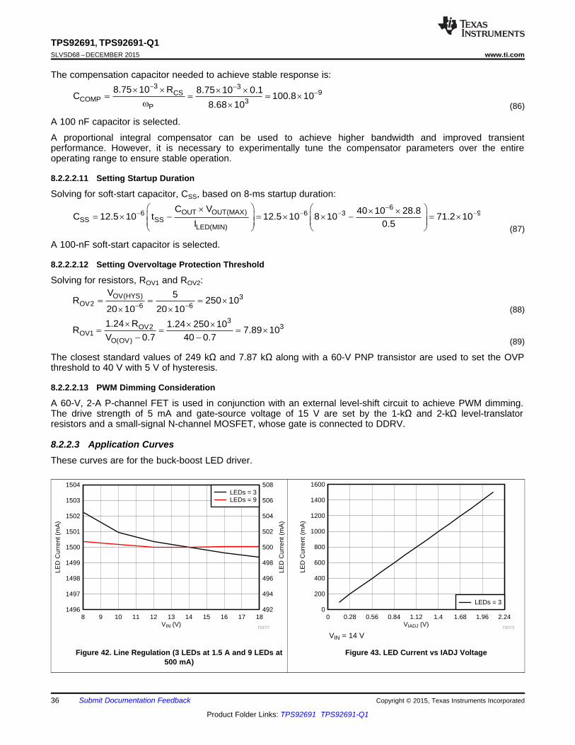
VIN (V)
LED
Cur
rent
(m
A)
LED
Cur
rent
(m
A)
8 9 10 11 12 13 14 15 16 17 181496 492
1497 494
1498 496
1499 498
1500 500
1501 502
1502 504
1503 506
1504 508
D022
LEDs = 3LEDs = 9
VIADJ (V)
LED
Cur
rent
(m
A)
0 0.28 0.56 0.84 1.12 1.4 1.68 1.96 2.240
200
400
600
800
1000
1200
1400
1600
D023
LEDs = 3
33OV2
OV1O(OV)
1.24 R 1.24 250 10R 7.89 10
V 0.7 40 0.7
u u u u
� �
OV(HYS) 3OV2 6 6
V 5R 250 10
20 10 20 10� � u
u u
6OUT OUT(MAX)6 6 3 9
SS SSLED(MIN)
C V 40 10 28.8C 12.5 10 t 12.5 10 8 10 71.2 10
I 0.5
�� � � �§ · § ·u u u
u � u u � u¨ ¸ ¨ ¸¨ ¸¨ ¸© ¹© ¹
3 39CS
COMP 3P
8.75 10 R 8.75 10 0.1C 100.8 10
8.68 10
� �
�u u u u u
Z u
TPS92691, TPS92691-Q1SLVSD68 –DECEMBER 2015 www.ti.com
The compensation capacitor needed to achieve stable response is:
(86)
A 100 nF capacitor is selected.
A proportional integral compensator can be used to achieve higher bandwidth and improved transientperformance. However, it is necessary to experimentally tune the compensator parameters over the entireoperating range to ensure stable operation.
8.2.2.2.11 Setting Startup Duration
Solving for soft-start capacitor, CSS, based on 8-ms startup duration:
(87)
A 100-nF soft-start capacitor is selected.
8.2.2.2.12 Setting Overvoltage Protection Threshold
Solving for resistors, ROV1 and ROV2:
(88)
(89)
The closest standard values of 249 kΩ and 7.87 kΩ along with a 60-V PNP transistor are used to set the OVPthreshold to 40 V with 5 V of hysteresis.
8.2.2.2.13 PWM Dimming Consideration
A 60-V, 2-A P-channel FET is used in conjunction with an external level-shift circuit to achieve PWM dimming.The drive strength of 5 mA and gate-source voltage of 15 V are set by the 1-kΩ and 2-kΩ level-translatorresistors and a small-signal N-channel MOSFET, whose gate is connected to DDRV.
8.2.2.3 Application CurvesThese curves are for the buck-boost LED driver.
VIN = 14 V
Figure 42. Line Regulation (3 LEDs at 1.5 A and 9 LEDs at Figure 43. LED Current vs IADJ Voltage500 mA)
36 Submit Documentation Feedback Copyright © 2015, Texas Instruments Incorporated
Product Folder Links: TPS92691 TPS92691-Q1

ILED (mA)
Effi
ency
(%
)
100 200 300 400 500 700 1000 200040
50
60
70
80
90
100100
D024
LEDs = 3LEDs = 5LEDs = 7LEDs = 9
TPS92691, TPS92691-Q1www.ti.com SLVSD68 –DECEMBER 2015
VIN = 14 V
Figure 44. Efficiency from 100 mA to 1.5 A
9 Power Supply RecommendationsThis device is designed to operate from an input voltage supply range between 4.5 V and 65 V. The input couldbe a car battery or another preregulated power supply. If the input supply is located more than a few inches fromthe TPS92691/-Q1 device, additional bulk capacitance or an input filter may be required in addition to theceramic bypass capacitors to address noise and EMI concerns.
10 Layout
10.1 Layout Guidelines• The performance of the switching regulator depends as much on the layout of the PCB as the component
selection. Following a few simple guidelines will maximize noise rejection and minimize the generation of EMIwithin the circuit.
• Discontinuous currents are the most likely to generate EMI. Therefore, take care when routing these paths.The main path for discontinuous current in the TPS92691/-Q1 Buck regulator contains the input capacitor,CIN, the recirculating diode, D, the N-channel MOSFET, Q1, and the sense resistor, RIS. In the TPS92691/-Q1Boost regulator, the discontinuous current flows through the output capacitor COUT, diode, D, N-channelMOSFET, Q1, and the current sense resistor, RIS. In Buck-Boost regulator, both loops are discontinuous andshould be carefully laid out. These loops should be kept as small as possible and the connection between allthe components should be short and thick to minimize parasitic inductance. In particular, the switch node(where L, D, and Q1 connect) should be just large enough to connect the components. To minimizeexcessive heating, large copper pours can be placed adjacent to the short current path of the switch node.
• CSP and CSN traces should be routed together with Kelvin connections to the current sense resistor as shortas possible. If needed, use common mode and differential mode noise filters to attenuate switching and diodereverse recovery noise from affecting the internal current sense amplifier.
• The COMP, IS, OVP, PWM, and IADJ pins are all high-impedance inputs that couple external noise easily;therefore, the loops containing these nodes should be minimized whenever possible.
• In some applications, the LED or LED array can be far away from the TPS92691/-Q1, or on a separate PCBconnected by a wiring harness. When an output capacitor is used and the LED array is large or separatedfrom the rest of the regulator, the output capacitor should be placed close to the LEDs to reduce the effects ofparasitic inductance on the AC impedance of the capacitor.
• The TPS92691/-Q1 has an exposed thermal pad to aid power dissipation. Adding several vias under theexposed pad helps conduct heat away from the device. The junction-to-ambient thermal resistance varieswith application. The most significant variables are the area of copper in the PCB and the number of viasunder the exposed pad. The integrity of the solder connection from the device exposed pad to the PCB iscritical. Excessive voids greatly decrease the thermal dissipation capacity.
Copyright © 2015, Texas Instruments Incorporated Submit Documentation Feedback 37
Product Folder Links: TPS92691 TPS92691-Q1

TP
S92
691Q
VIN
RT/SY
PWM
SS
IADJ
IMON
COMP
AGND
INP
UT
CO
NN
VCC
IS
PGND
GATE
DDRV
CSP
OVP
CSN
VINLED+
LED+GND
BU
CK
-BO
OS
T
BO
OS
T
VIA TO BOTTOM GROUND PLANE
TPS92691, TPS92691-Q1SLVSD68 –DECEMBER 2015 www.ti.com
10.2 Layout Example
Figure 45. Layout Recommendation
38 Submit Documentation Feedback Copyright © 2015, Texas Instruments Incorporated
Product Folder Links: TPS92691 TPS92691-Q1

TPS92691, TPS92691-Q1www.ti.com SLVSD68 –DECEMBER 2015
11 Device and Documentation Support
11.1 Related LinksThe table below lists quick access links. Categories include technical documents, support and communityresources, tools and software, and quick access to sample or buy.
Table 5. Related LinksTECHNICAL TOOLS & SUPPORT &PARTS PRODUCT FOLDER SAMPLE & BUY DOCUMENTS SOFTWARE COMMUNITY
TPS92691 Click here Click here Click here Click here Click hereTPS92691-Q1 Click here Click here Click here Click here Click here
11.2 Community ResourcesThe following links connect to TI community resources. Linked contents are provided "AS IS" by the respectivecontributors. They do not constitute TI specifications and do not necessarily reflect TI's views; see TI's Terms ofUse.
TI E2E™ Online Community TI's Engineer-to-Engineer (E2E) Community. Created to foster collaborationamong engineers. At e2e.ti.com, you can ask questions, share knowledge, explore ideas and helpsolve problems with fellow engineers.
Design Support TI's Design Support Quickly find helpful E2E forums along with design support tools andcontact information for technical support.
11.3 TrademarksPowerPAD, E2E are trademarks of Texas Instruments.All other trademarks are the property of their respective owners.
11.4 Electrostatic Discharge CautionThese devices have limited built-in ESD protection. The leads should be shorted together or the device placed in conductive foamduring storage or handling to prevent electrostatic damage to the MOS gates.
11.5 GlossarySLYZ022 — TI Glossary.
This glossary lists and explains terms, acronyms, and definitions.
12 Mechanical, Packaging, and Orderable InformationThe following pages include mechanical, packaging, and orderable information. This information is the mostcurrent data available for the designated devices. This data is subject to change without notice and revision ofthis document. For browser-based versions of this data sheet, refer to the left-hand navigation.
Copyright © 2015, Texas Instruments Incorporated Submit Documentation Feedback 39
Product Folder Links: TPS92691 TPS92691-Q1

PACKAGE OPTION ADDENDUM
www.ti.com 17-Dec-2015
Addendum-Page 1
PACKAGING INFORMATION
Orderable Device Status(1)
Package Type PackageDrawing
Pins PackageQty
Eco Plan(2)
Lead/Ball Finish(6)
MSL Peak Temp(3)
Op Temp (°C) Device Marking(4/5)
Samples
TPS92691PWP ACTIVE HTSSOP PWP 16 90 Green (RoHS& no Sb/Br)
CU NIPDAU Level-3-260C-168 HR -40 to 125 92691
TPS92691PWPR ACTIVE HTSSOP PWP 16 2000 Green (RoHS& no Sb/Br)
CU NIPDAU Level-3-260C-168 HR -40 to 125 92691
TPS92691QPWPQ1 ACTIVE HTSSOP PWP 16 90 Green (RoHS& no Sb/Br)
CU NIPDAU Level-3-260C-168 HR -40 to 125 92691Q
TPS92691QPWPRQ1 ACTIVE HTSSOP PWP 16 2000 Green (RoHS& no Sb/Br)
CU NIPDAU Level-3-260C-168 HR -40 to 125 92691Q
TPS92691QPWPTQ1 ACTIVE HTSSOP PWP 16 250 Green (RoHS& no Sb/Br)
CU NIPDAU Level-3-260C-168 HR -40 to 125 92691Q
(1) The marketing status values are defined as follows:ACTIVE: Product device recommended for new designs.LIFEBUY: TI has announced that the device will be discontinued, and a lifetime-buy period is in effect.NRND: Not recommended for new designs. Device is in production to support existing customers, but TI does not recommend using this part in a new design.PREVIEW: Device has been announced but is not in production. Samples may or may not be available.OBSOLETE: TI has discontinued the production of the device.
(2) Eco Plan - The planned eco-friendly classification: Pb-Free (RoHS), Pb-Free (RoHS Exempt), or Green (RoHS & no Sb/Br) - please check http://www.ti.com/productcontent for the latest availabilityinformation and additional product content details.TBD: The Pb-Free/Green conversion plan has not been defined.Pb-Free (RoHS): TI's terms "Lead-Free" or "Pb-Free" mean semiconductor products that are compatible with the current RoHS requirements for all 6 substances, including the requirement thatlead not exceed 0.1% by weight in homogeneous materials. Where designed to be soldered at high temperatures, TI Pb-Free products are suitable for use in specified lead-free processes.Pb-Free (RoHS Exempt): This component has a RoHS exemption for either 1) lead-based flip-chip solder bumps used between the die and package, or 2) lead-based die adhesive used betweenthe die and leadframe. The component is otherwise considered Pb-Free (RoHS compatible) as defined above.Green (RoHS & no Sb/Br): TI defines "Green" to mean Pb-Free (RoHS compatible), and free of Bromine (Br) and Antimony (Sb) based flame retardants (Br or Sb do not exceed 0.1% by weightin homogeneous material)
(3) MSL, Peak Temp. - The Moisture Sensitivity Level rating according to the JEDEC industry standard classifications, and peak solder temperature.
(4) There may be additional marking, which relates to the logo, the lot trace code information, or the environmental category on the device.
(5) Multiple Device Markings will be inside parentheses. Only one Device Marking contained in parentheses and separated by a "~" will appear on a device. If a line is indented then it is a continuationof the previous line and the two combined represent the entire Device Marking for that device.
PACKAGE OPTION ADDENDUM
www.ti.com 17-Dec-2015
Addendum-Page 2
(6) Lead/Ball Finish - Orderable Devices may have multiple material finish options. Finish options are separated by a vertical ruled line. Lead/Ball Finish values may wrap to two lines if the finishvalue exceeds the maximum column width.
Important Information and Disclaimer:The information provided on this page represents TI's knowledge and belief as of the date that it is provided. TI bases its knowledge and belief on informationprovided by third parties, and makes no representation or warranty as to the accuracy of such information. Efforts are underway to better integrate information from third parties. TI has taken andcontinues to take reasonable steps to provide representative and accurate information but may not have conducted destructive testing or chemical analysis on incoming materials and chemicals.TI and TI suppliers consider certain information to be proprietary, and thus CAS numbers and other limited information may not be available for release.
In no event shall TI's liability arising out of such information exceed the total purchase price of the TI part(s) at issue in this document sold by TI to Customer on an annual basis.
OTHER QUALIFIED VERSIONS OF TPS92691, TPS92691-Q1 :
• Catalog: TPS92691
• Automotive: TPS92691-Q1
NOTE: Qualified Version Definitions:
• Catalog - TI's standard catalog product
• Automotive - Q100 devices qualified for high-reliability automotive applications targeting zero defects
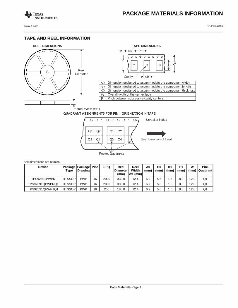
TAPE AND REEL INFORMATION
*All dimensions are nominal
Device PackageType
PackageDrawing
Pins SPQ ReelDiameter
(mm)
ReelWidth
W1 (mm)
A0(mm)
B0(mm)
K0(mm)
P1(mm)
W(mm)
Pin1Quadrant
TPS92691PWPR HTSSOP PWP 16 2000 330.0 12.4 6.9 5.6 1.6 8.0 12.0 Q1
TPS92691QPWPRQ1 HTSSOP PWP 16 2000 330.0 12.4 6.9 5.6 1.6 8.0 12.0 Q1
TPS92691QPWPTQ1 HTSSOP PWP 16 250 180.0 12.4 6.9 5.6 1.6 8.0 12.0 Q1
PACKAGE MATERIALS INFORMATION
www.ti.com 13-Feb-2016
Pack Materials-Page 1

*All dimensions are nominal
Device Package Type Package Drawing Pins SPQ Length (mm) Width (mm) Height (mm)
TPS92691PWPR HTSSOP PWP 16 2000 367.0 367.0 38.0
TPS92691QPWPRQ1 HTSSOP PWP 16 2000 367.0 367.0 38.0
TPS92691QPWPTQ1 HTSSOP PWP 16 250 210.0 185.0 35.0
PACKAGE MATERIALS INFORMATION
www.ti.com 13-Feb-2016
Pack Materials-Page 2

www.ti.com
PACKAGE OUTLINE
C
14X 0.65
2X4.55
16X 0.300.19
TYP6.66.2
0.150.05
0.25GAGE PLANE
-80
1.2 MAX3.552.68
2.461.75
B 4.54.3
A
NOTE 3
5.14.9
0.750.50
(0.15) TYP
PowerPAD TSSOP - 1.2 mm max heightPWP0016JSMALL OUTLINE PACKAGE
4223595/A 03/2017
1
89
16
0.1 C A B
PIN 1 INDEXAREA
SEE DETAIL A
0.1 C
NOTES: 1. All linear dimensions are in millimeters. Any dimensions in parenthesis are for reference only. Dimensioning and tolerancing per ASME Y14.5M. 2. This drawing is subject to change without notice. 3. This dimension does not include mold flash, protrusions, or gate burrs. Mold flash, protrusions, or gate burrs shall not exceed 0.15 mm per side. 4. Reference JEDEC registration MO-153.
SEATINGPLANE
TM
PowerPAD is a trademark of Texas Instruments.
A 20DETAIL ATYPICAL
SCALE 2.500
THERMALPAD
1
8 9
16

www.ti.com
EXAMPLE BOARD LAYOUT
0.05 MAXALL AROUND
0.05 MINALL AROUND
16X (1.5)
16X (0.45)
14X (0.65)
(5.8)
(R0.05) TYP
(3.4)NOTE 8
(5)NOTE 8
(1.35) TYP
(0.65)
(1.3) TYP
( 0.2) TYPVIA
(2.46)
(3.55)
PowerPAD TSSOP - 1.2 mm max heightPWP0016JSMALL OUTLINE PACKAGE
4223595/A 03/2017
NOTES: (continued) 5. Publication IPC-7351 may have alternate designs. 6. Solder mask tolerances between and around signal pads can vary based on board fabrication site. 7. This package is designed to be soldered to a thermal pad on the board. For more information, see Texas Instruments literature numbers SLMA002 (www.ti.com/lit/slma002) and SLMA004 (www.ti.com/lit/slma004). 8. Size of metal pad may vary due to creepage requirement. 9. Vias are optional depending on application, refer to device data sheet. It is recommended that vias under paste be filled, plugged or tented.
TM
SEE DETAILS
LAND PATTERN EXAMPLEEXPOSED METAL SHOWN
SCALE: 10X
SYMM
SYMM
1
8 9
16
METAL COVEREDBY SOLDER MASK
SOLDER MASKDEFINED PAD
15.000
METALSOLDER MASKOPENING
METAL UNDERSOLDER MASK
SOLDER MASKOPENING
EXPOSED METALEXPOSED METAL
SOLDER MASK DETAILS
NON-SOLDER MASKDEFINED
SOLDER MASKDEFINED

www.ti.com
EXAMPLE STENCIL DESIGN
16X (1.5)
16X (0.45)
14X (0.65)
(5.8)
(R0.05) TYP
(3.55)BASED ON
0.125 THICKSTENCIL
(2.46)BASED ON
0.125 THICKSTENCIL
PowerPAD TSSOP - 1.2 mm max heightPWP0016JSMALL OUTLINE PACKAGE
4223595/A 03/2017
2.08 X 3.000.1752.25 X 3.240.15
2.46 X 3.55 (SHOWN)0.1252.75 X 3.970.1
SOLDER STENCILOPENING
STENCILTHICKNESS
NOTES: (continued) 10. Laser cutting apertures with trapezoidal walls and rounded corners may offer better paste release. IPC-7525 may have alternate design recommendations. 11. Board assembly site may have different recommendations for stencil design.
TM
SOLDER PASTE EXAMPLEBASED ON 0.125 mm THICK STENCIL
SCALE: 10X
SYMM
SYMM
1
8 9
16
METAL COVEREDBY SOLDER MASK
SEE TABLE FORDIFFERENT OPENINGSFOR OTHER STENCILTHICKNESSES

IMPORTANT NOTICE
Texas Instruments Incorporated (TI) reserves the right to make corrections, enhancements, improvements and other changes to itssemiconductor products and services per JESD46, latest issue, and to discontinue any product or service per JESD48, latest issue. Buyersshould obtain the latest relevant information before placing orders and should verify that such information is current and complete.TI’s published terms of sale for semiconductor products (http://www.ti.com/sc/docs/stdterms.htm) apply to the sale of packaged integratedcircuit products that TI has qualified and released to market. Additional terms may apply to the use or sale of other types of TI products andservices.Reproduction of significant portions of TI information in TI data sheets is permissible only if reproduction is without alteration and isaccompanied by all associated warranties, conditions, limitations, and notices. TI is not responsible or liable for such reproduceddocumentation. Information of third parties may be subject to additional restrictions. Resale of TI products or services with statementsdifferent from or beyond the parameters stated by TI for that product or service voids all express and any implied warranties for theassociated TI product or service and is an unfair and deceptive business practice. TI is not responsible or liable for any such statements.Buyers and others who are developing systems that incorporate TI products (collectively, “Designers”) understand and agree that Designersremain responsible for using their independent analysis, evaluation and judgment in designing their applications and that Designers havefull and exclusive responsibility to assure the safety of Designers' applications and compliance of their applications (and of all TI productsused in or for Designers’ applications) with all applicable regulations, laws and other applicable requirements. Designer represents that, withrespect to their applications, Designer has all the necessary expertise to create and implement safeguards that (1) anticipate dangerousconsequences of failures, (2) monitor failures and their consequences, and (3) lessen the likelihood of failures that might cause harm andtake appropriate actions. Designer agrees that prior to using or distributing any applications that include TI products, Designer willthoroughly test such applications and the functionality of such TI products as used in such applications.TI’s provision of technical, application or other design advice, quality characterization, reliability data or other services or information,including, but not limited to, reference designs and materials relating to evaluation modules, (collectively, “TI Resources”) are intended toassist designers who are developing applications that incorporate TI products; by downloading, accessing or using TI Resources in anyway, Designer (individually or, if Designer is acting on behalf of a company, Designer’s company) agrees to use any particular TI Resourcesolely for this purpose and subject to the terms of this Notice.TI’s provision of TI Resources does not expand or otherwise alter TI’s applicable published warranties or warranty disclaimers for TIproducts, and no additional obligations or liabilities arise from TI providing such TI Resources. TI reserves the right to make corrections,enhancements, improvements and other changes to its TI Resources. TI has not conducted any testing other than that specificallydescribed in the published documentation for a particular TI Resource.Designer is authorized to use, copy and modify any individual TI Resource only in connection with the development of applications thatinclude the TI product(s) identified in such TI Resource. NO OTHER LICENSE, EXPRESS OR IMPLIED, BY ESTOPPEL OR OTHERWISETO ANY OTHER TI INTELLECTUAL PROPERTY RIGHT, AND NO LICENSE TO ANY TECHNOLOGY OR INTELLECTUAL PROPERTYRIGHT OF TI OR ANY THIRD PARTY IS GRANTED HEREIN, including but not limited to any patent right, copyright, mask work right, orother intellectual property right relating to any combination, machine, or process in which TI products or services are used. Informationregarding or referencing third-party products or services does not constitute a license to use such products or services, or a warranty orendorsement thereof. Use of TI Resources may require a license from a third party under the patents or other intellectual property of thethird party, or a license from TI under the patents or other intellectual property of TI.TI RESOURCES ARE PROVIDED “AS IS” AND WITH ALL FAULTS. TI DISCLAIMS ALL OTHER WARRANTIES ORREPRESENTATIONS, EXPRESS OR IMPLIED, REGARDING RESOURCES OR USE THEREOF, INCLUDING BUT NOT LIMITED TOACCURACY OR COMPLETENESS, TITLE, ANY EPIDEMIC FAILURE WARRANTY AND ANY IMPLIED WARRANTIES OFMERCHANTABILITY, FITNESS FOR A PARTICULAR PURPOSE, AND NON-INFRINGEMENT OF ANY THIRD PARTY INTELLECTUALPROPERTY RIGHTS. TI SHALL NOT BE LIABLE FOR AND SHALL NOT DEFEND OR INDEMNIFY DESIGNER AGAINST ANY CLAIM,INCLUDING BUT NOT LIMITED TO ANY INFRINGEMENT CLAIM THAT RELATES TO OR IS BASED ON ANY COMBINATION OFPRODUCTS EVEN IF DESCRIBED IN TI RESOURCES OR OTHERWISE. IN NO EVENT SHALL TI BE LIABLE FOR ANY ACTUAL,DIRECT, SPECIAL, COLLATERAL, INDIRECT, PUNITIVE, INCIDENTAL, CONSEQUENTIAL OR EXEMPLARY DAMAGES INCONNECTION WITH OR ARISING OUT OF TI RESOURCES OR USE THEREOF, AND REGARDLESS OF WHETHER TI HAS BEENADVISED OF THE POSSIBILITY OF SUCH DAMAGES.Unless TI has explicitly designated an individual product as meeting the requirements of a particular industry standard (e.g., ISO/TS 16949and ISO 26262), TI is not responsible for any failure to meet such industry standard requirements.Where TI specifically promotes products as facilitating functional safety or as compliant with industry functional safety standards, suchproducts are intended to help enable customers to design and create their own applications that meet applicable functional safety standardsand requirements. Using products in an application does not by itself establish any safety features in the application. Designers mustensure compliance with safety-related requirements and standards applicable to their applications. Designer may not use any TI products inlife-critical medical equipment unless authorized officers of the parties have executed a special contract specifically governing such use.Life-critical medical equipment is medical equipment where failure of such equipment would cause serious bodily injury or death (e.g., lifesupport, pacemakers, defibrillators, heart pumps, neurostimulators, and implantables). Such equipment includes, without limitation, allmedical devices identified by the U.S. Food and Drug Administration as Class III devices and equivalent classifications outside the U.S.TI may expressly designate certain products as completing a particular qualification (e.g., Q100, Military Grade, or Enhanced Product).Designers agree that it has the necessary expertise to select the product with the appropriate qualification designation for their applicationsand that proper product selection is at Designers’ own risk. Designers are solely responsible for compliance with all legal and regulatoryrequirements in connection with such selection.Designer will fully indemnify TI and its representatives against any damages, costs, losses, and/or liabilities arising out of Designer’s non-compliance with the terms and provisions of this Notice.
Mailing Address: Texas Instruments, Post Office Box 655303, Dallas, Texas 75265Copyright © 2017, Texas Instruments Incorporated