tps7a90 500-ma, high-accuracy, low-noise ldo … · out 1 10 in out 2 9 in fb 3 8 nr/ss gnd 4 7 en...
TRANSCRIPT

TPS7A90
Clock
SCLK
ADC
OUT
VDD
PG
ENABLE
VDD_VCO
IN
EN
VIN
EN
LMK03328LMX2581
ADC3xxxADC3xJxxADC3xJBxxADS4xxBxxADS5xJxxADS12Jxxxx
CIN
COUT
GND
Copyright © 2017, Texas Instruments Incorporated
1.2 V2.0 V OUT
PG
IN
EN
TPS7A90
SS_CTRL
NR/SS
FBCIN
10 PFCOUT
10 F
CNR/SS
0.1 PF
R1
R2
11.8 k:
5.9 k:
VOUT
RPG
20 k:PG
GND
CFF 10 nF
Copyright © 2017, Texas Instruments Incorporated
Product
Folder
Order
Now
Technical
Documents
Tools &
Software
Support &Community
An IMPORTANT NOTICE at the end of this data sheet addresses availability, warranty, changes, use in safety-critical applications,intellectual property matters and other important disclaimers. PRODUCTION DATA.
TPS7A90SBVS324 –JUNE 2017
TPS7A90500-mA, High-Accuracy, Low-Noise LDO Voltage Regulator
1
1 Features1• 1.0% Accuracy Over Line, Load, and Temperature• Low Output Noise: 4.7 µVRMS (10 Hz–100 kHz)• Low Dropout: 100 mV (max) at 0.5 A• Wide Input Voltage Range: 1.4 V to 6.5 V• Wide Output Voltage Range: 0.8 V to 5.7 V• High Power-Supply Rejection Ratio (PSRR):
– 60 dB at DC– 50 dB at 100 kHz– 30 dB at 1 MHz
• Fast Transient Response• Adjustable Start-Up In-Rush Control With
Selectable Soft-Start Charging Current• Open-Drain Power-Good (PG) Output• θJC = 3.2ºC/W• 2.5-mm × 2.5-mm, 10-Pin WSON Package
2 Applications• High-Speed Analog Circuits:
– VCO, ADC, DAC, LVDS• Imaging: CMOS Sensors, Video ASICs• Test and Measurement• Instrumentation, Medical, and Audio• Digital Loads: SerDes, FPGA, DSP
3 DescriptionThe TPS7A90 device is a low-noise (4.7 µVRMS), low-dropout (LDO) voltage regulator capable of sourcing500 mA with only 100 mV of maximum dropout to 5 Vand 200 mV to 5.7 V.
The TPS7A90 output is adjustable with externalresistors from 0.8 V to 5.7 V. The TPS7A90 wideinput voltage range supports operation as low as1.4 V and up to 6.5 V.
With 1% output voltage accuracy (over line, load, andtemperature) and soft-start capabilities to reduce in-rush current, the TPS7A90 is ideal for poweringsensitive analog low-voltage devices [such asvoltage-controlled oscillators (VCOs), analog-to-digitalconverters (ADCs), and digital-to-analog converters(DACs)].
The TPS7A90 is designed to power noise-sensitivecomponents such as those found in high-speedcommunication, video, medical, or test andmeasurement applications. The very low 4.7-µVRMSoutput noise and wideband PSRR (30 dB at 1 MHz)minimizes phase noise and clock jitter. Thesefeatures maximize performance of clocking devices,ADCs, and DACs.
Device Information(1)
PART NUMBER PACKAGE BODY SIZE (NOM)TPS7A90 WSON (10) 2.50 mm × 2.50 mm
(1) For all available packages, see the orderable addendum atthe end of the datasheet.
Typical Application Circuit Typical Application Diagram

2
TPS7A90SBVS324 –JUNE 2017 www.ti.com
Product Folder Links: TPS7A90
Submit Documentation Feedback Copyright © 2017, Texas Instruments Incorporated
Table of Contents1 Features .................................................................. 12 Applications ........................................................... 13 Description ............................................................. 14 Revision History..................................................... 25 Pin Configuration and Functions ......................... 36 Specifications......................................................... 3
6.1 Absolute Maximum Ratings ...................................... 36.2 ESD Ratings.............................................................. 46.3 Recommended Operating Conditions....................... 46.4 Thermal Information .................................................. 46.5 Electrical Characteristics........................................... 56.6 Typical Characteristics .............................................. 6
7 Detailed Description ............................................ 127.1 Overview ................................................................. 127.2 Functional Block Diagram ....................................... 127.3 Feature Description................................................. 127.4 Device Functional Modes........................................ 16
8 Application and Implementation ........................ 178.1 Application Information............................................ 178.2 Typical Application .................................................. 21
9 Power Supply Recommendations ...................... 2210 Layout................................................................... 22
10.1 Layout Guidelines ................................................. 2210.2 Layout Example .................................................... 23
11 Device and Documentation Support ................. 2411.1 Device Support .................................................... 2411.2 Documentation Support ........................................ 2411.3 Receiving Notification of Documentation Updates 2411.4 Community Resources.......................................... 2511.5 Trademarks ........................................................... 2511.6 Electrostatic Discharge Caution............................ 2511.7 Glossary ................................................................ 25
12 Mechanical, Packaging, and OrderableInformation ........................................................... 25
4 Revision HistoryNOTE: Page numbers for previous revisions may differ from page numbers in the current version.
DATE REVISION NOTESJune 2017 * Initial release.

1OUT 10 IN
2OUT 9 IN
3FB 8 NR/SS
4GND 7 EN
5PG 6 SS_CTRL
Not to scale
ThermalPad
3
TPS7A90www.ti.com SBVS324 –JUNE 2017
Product Folder Links: TPS7A90
Submit Documentation FeedbackCopyright © 2017, Texas Instruments Incorporated
5 Pin Configuration and Functions
DSK Package2.5-mm × 2.5-mm, 10-Pin WSON
Top View
Pin FunctionsPIN
DESCRIPTIONNAME NO. I/O
EN 7 I Enable pin. This pin turns the LDO on and off. If VEN ≥ VIH(EN), the regulator is enabled. If VEN ≤ VIL(EN),the regulator is disabled. The EN pin must be connected to IN if the enable function is not used.
FB 3 I Feedback pin.This pin is the input to the control loop error amplifier and is used to set the output voltage of the device.
GND 4 — Device GND. Connect to the device thermal pad.
IN 9, 10 I Input pin. A 10-µF or greater input capacitor is required.
NR/SS 8 —Noise reduction pin.Connect this pin to an external capacitor to bypass the noise generated by the internal band-gap reference. Thecapacitor reduces the output noise to very low levels and sets the output ramp rate to limit in-rush current.
OUT 1, 2 O Regulated output. A 10-µF or greater capacitor must be connected from this pin to GND for stability.
PG 5 O Open-drain, power-good indicator pin for the LDO output voltage. A 10-kΩ to 100-kΩ external pullup resistor isrequired. This pin can be left floating or connected to GND if not used.
SS_CTRL 6 I Soft-start control pin. Connect this pin either to GND or IN to change the NR/SS capacitor charging current.If a CNR/SS capacitor is not used, SS_CTRL must be connected to GND to avoid output overshoot.
Thermal pad Pad — Connect the thermal pad to the printed circuit board (PCB) ground plane. For an example layout, see Figure 42.
(1) Stresses beyond those listed under Absolute Maximum Ratings may cause permanent damage to the device. These are stress ratingsonly, which do not imply functional operation of the device at these or any other conditions beyond those indicated under RecommendedOperating Conditions. Exposure to absolute-maximum-rated conditions for extended periods may affect device reliability.
6 Specifications
6.1 Absolute Maximum Ratingsover operating junction temperature range and all voltages with respect to GND (unless otherwise noted) (1)
MIN MAX UNIT
Voltage
IN, PG, EN –0.3 7.0
VIN, PG, EN (5% duty cycle, pulse duration ≤ 200 µs) –0.3 7.5OUT –0.3 VIN + 0.3SS_CTRL –0.3 VIN + 0.3NR/SS, FB –0.3 3.6
CurrentOUT Internally limited APG (sink current into the device) 5 mA
TemperatureOperating junction, TJ –55 150 °CStorage, Tstg –55 150 °C

4
TPS7A90SBVS324 –JUNE 2017 www.ti.com
Product Folder Links: TPS7A90
Submit Documentation Feedback Copyright © 2017, Texas Instruments Incorporated
(1) JEDEC document JEP155 states that 500-V HBM allows safe manufacturing with a standard ESD control process.(2) JEDEC document JEP157 states that 250-V CDM allows safe manufacturing with a standard ESD control process.
6.2 ESD RatingsVALUE UNIT
V(ESD) Electrostatic dischargeHuman body model (HBM), per ANSI/ESDA/JEDEC JS-001 (1) ±2000
VCharged device model (CDM), per JEDEC specification JESD22-C101 (2) ±500
6.3 Recommended Operating Conditionsover operating junction temperature range (unless otherwise noted)
MIN MAX UNITVIN Input supply voltage range 1.4 6.5 VVOUT Output voltage range 0.8 5.7 VIOUT Output current 0 0.5 ACIN Input capacitor 10 µFCOUT Output capacitor 10 µFCNR/SS Noise-reduction capacitor 0 10 µFCFF Feedforward capacitor 0 100 nFRPG Power-good pullup resistance 10 100 kΩTJ Junction temperature –40 125 °C
(1) For more information about traditional and new thermal metrics, see the Semiconductor and IC Package Thermal Metrics applicationreport.
6.4 Thermal Information
THERMAL METRIC (1)TPS7A90
UNITDSK (SON)10 PINS
RθJA Junction-to-ambient thermal resistance 56.9 °C/WRθJC(top) Junction-to-case (top) thermal resistance 46.3 °C/WRθJB Junction-to-board thermal resistance 29.1 °C/WψJT Junction-to-top characterization parameter 0.8 °C/WψJB Junction-to-board characterization parameter 29.4 °C/WRθJC(bot) Junction-to-case (bottom) thermal resistance 3.2 °C/W

5
TPS7A90www.ti.com SBVS324 –JUNE 2017
Product Folder Links: TPS7A90
Submit Documentation FeedbackCopyright © 2017, Texas Instruments Incorporated
(1) When the device is connected to external feedback resistors at the FB pin, external resistor tolerances are not included.(2) The device is not tested under conditions where VIN > VOUT + 2.5 V and IOUT = 0.5 A because the power dissipation is higher than the
maximum rating of the package. Also, this accuracy specification does not apply on any application condition that exceeds the powerdissipation limit of the package under test.
6.5 Electrical Characteristicsover operating temperature range (TJ = –40°C to +125°C), 1.4 V ≤ VIN ≤ 6.5 V, VOUT(NOM) = 0.8 V, IOUT = 5 mA, VEN = 1.4 V,CIN = COUT = 10 μF, CNR/SS = CFF = 0 nF, SS_CTRL = GND, and PG pin pulled up to VIN with 100 kΩ (unless otherwisenoted); typical values are at TJ = 25°C
PARAMETER TEST CONDITIONS MIN TYP MAX UNIT
VIN Input supply voltage range 1.4 6.5 V
VREF Reference voltage 0.8 V
VUVLO Input supply UVLO VIN rising 1.31 1.39 V
VHYS(UVLO) Input supply UVLO hysteresis 290 mV
VOUTOutput voltage range 0.8 5.7 V
Output voltage accuracy (1) 1.4 V ≤ VIN ≤ 6.5 V, 5 mA ≤ IOUT ≤ 0.5 A –1.0% 1.0%
ΔVOUT(ΔVIN) Line regulation 0.005 %/V
ΔVOUT(ΔIOUT) Load regulation (2) 5 mA ≤ IOUT ≤ 0.5 A 0.02 %/A
VDO Dropout voltage1.4 V ≤ VIN ≤ 5.0 V, IOUT = 0.5 A, VFB = 0.8 V – 3% 100
mV5.0 V < VIN ≤ 5.7 V, IOUT = 0.5 A, VFB = 0.8 V – 3% 200
ILIM Output current limit VOUT forced at 0.9 × VOUT(NOM),VIN = VOUT(NOM) + 300 mV 0.8 1.1 1.5 A
IGND GND pin currentVIN = 6.5 V, IOUT = 5 mA 2.1 3.5
mAVIN = 1.4 V, IOUT = 0.5 A 4
ISDN Shutdown GND pin current PG = (open), VIN = 6.5 V, VEN = 0.4 V 0.1 15 µA
IEN EN pin current VIN = 6.5 V, 0 V ≤ VEN ≤ 6.5 V –0.2 0.2 µA
VIL(EN)EN pin low-level input voltage(device disabled) 0 0.4 V
VIH(EN)EN pin high-level input voltage(device enabled) 1.1 6.5 V
ISS_CTRL SS_CTRL pin current VIN = 6.5 V, 0 V ≤ VSS_CTRL ≤ 6.5 V –0.2 0.2 µA
VIT(PG) PG pin threshold For PG transitioning low with falling VOUT, expressed asa percentage of VOUT(NOM)
82% 88.9% 93%
VHYS(PG) PG pin hysteresis For PG transitioning high with rising VOUT, expressed asa percentage of VOUT(NOM)
1%
VOL(PG) PG pin low-level output voltage VOUT < VIT(PG), IPG = –1 mA (current into device) 0.4 V
ILKG(PG) PG pin leakage current VOUT > VIT(PG), VPG = 6.5 V 1 µA
INR/SS NR/SS pin charging currentVNR/SS = GND, VSS_CTRL = GND 4.0 6.2 9.0
µAVNR/SS = GND, VSS_CTRL = VIN 65 100 150
IFB FB pin leakage current VIN = 6.5 V, VFB = 0.8 V –100 100 nA
PSRR Power-supply ripple rejection f = 500 kHz, VIN = 3.8 V, VOUT(NOM) = 3.3 V,IOUT = 250mA, CNR/SS = 10 nF, CFF = 10 nF 39 dB
Vn Output noise voltage BW = 10 Hz to 100 kHz, VIN = 1.8 V, VOUT(NOM) = 0.8 V,IOUT = 0.5 A, CNR/SS = 10 nF, CFF = 10 nF 4.7 µVRMS
Noise spectral density f = 10 kHz, VIN = 1.8 V, VOUT(NOM) = 0.8 V,IOUT = 0.5 A, CNR/SS = 10 nF, CFF = 10 nF 13 nV/√Hz
RdissOutput active dischargeresistance VEN = GND 250 Ω
Tsd Thermal shutdown temperatureShutdown, temperature increasing 160
°CReset, temperature decreasing 140

Frequency (Hz)
Pow
er-S
uppl
y R
ejec
tion
Rat
io (
dB)
0
10
20
30
40
50
60
70
10 100 1k 10k 100k 1M 10M
IOUT = 10 mAIOUT = 50 mAIOUT = 100 mA
IOUT = 250 mAIOUT = 500 mA
Frequency (Hz)
Pow
er-S
uppl
y R
ejec
tion
Rat
io (
dB)
0
10
20
30
40
50
60
70
10 100 1k 10k 100k 1M 10M
IOUT = 10 mAIOUT = 50 mAIOUT = 100 mA
IOUT = 250 mAIOUT = 500 mA
Frequency (Hz)
Pow
er-S
uppl
y R
ejec
tion
Rat
io (
dB)
0
10
20
30
40
50
60
70
10 100 1k 10k 100k 1M 10M
VIN3.5 V3.6 V3.7 V
3.8 V4.0 V4.3 V
Frequency (Hz)
Pow
er-S
uppl
y R
ejec
tion
Rat
io (
dB)
0
10
20
30
40
50
60
70
10 100 1k 10k 100k 1M 10M10 100 1k 10k 100k 1M 10M
VIN5.2 V5.3 V5.4 V
5.5 V6 V6.5 V
Frequency (Hz)
Pow
er-S
uppl
y R
ejec
tion
Rat
io (
dB)
0
10
20
30
40
50
60
70
10 100 1k 10k 100k 1M 10M
VIN1.4 V1.5 V1.8 V
2.0 V2.5 V3.0 V
Frequency (Hz)
Pow
er-S
uppl
y R
ejec
tion
Rat
io (
dB)
0
10
20
30
40
50
60
70
10 100 1k 10k 100k 1M 10M
VIN1.4 V1.5 V1.7 V2.0 V
2.2 V2.5 V3.0 V
6
TPS7A90SBVS324 –JUNE 2017 www.ti.com
Product Folder Links: TPS7A90
Submit Documentation Feedback Copyright © 2017, Texas Instruments Incorporated
6.6 Typical Characteristicsat TJ = 25°C, 1.4 V ≤ VIN ≤ 6.5 V, VIN ≥ VOUT(NOM) + 0.3 V, VOUT = 0.8 V, SS_CTRL = GND, IOUT = 5 mA, VEN = 1.1 V, COUT =10 μF, CNR/SS = CFF = 0 nF, PG pin pulled up to VOUT with 100 kΩ, and SS_CTRL = GND (unless otherwise noted)
VOUT = 0.8 V, IOUT = 500 mA, COUT = 10 µF,CNR/SS = CFF = 10 nF
Figure 1. PSRR vs Frequency and Input Voltage
VOUT = 1.2 V, IOUT = 500 mA, COUT = 10 µF,CNR/SS = CFF = 10 nF
Figure 2. PSRR vs Frequency and Input Voltage
VOUT = 3.3 V, IOUT = 500 mA, COUT = 10 µF,CNR/SS = CFF = 10 nF
Figure 3. PSRR vs Frequency and Input Voltage
VOUT = 5 V, IOUT = 500 mA, COUT = 10 µF,CNR/SS = CFF = 10 nF
Figure 4. PSRR vs Frequency and Input Voltage
VOUT = 1.2 V, VIN = VEN = 1.5 V, COUT = 10 µF,CNR/SS = CFF = 10 nF
Figure 5. PSRR vs Frequency and Output Current
VOUT = 3.3 V, VIN = VEN = 3.6 V, COUT = 10 µF,CNR/SS = CFF = 10 nF
Figure 6. PSRR vs Frequency and Output Current

Frequency (Hz)
Noi
se (PV
Hz)
0.001
0.01
0.1
1
10
10 100 1k 10k 100k 1M 10M
COUT10 PF, 5.2 PVRMS22 PF, 5.2 PVRMS100 PF, 6 PVRMS
Output Voltage (mV)
Cur
rent
Lim
it (A
)
0 100 200 300 400 500 600 700 8000.8
0.9
1
1.1
1.2
1.3
1.4
1.5
1.6Temperature
-40qC0qC
25qC85qC
125qC
Frequency (Hz)
Noi
se (PV
Hz)
0.001
0.01
0.1
1
10
10 100 1k 10k 100k 1M 10M
CNRNone, 10.5 PVRMS10 nF, 5.2 PVRMS100 nF, 4.8 PVRMS
1 PF, 4.7 PVRMS10µF, 4.7 PVRMS
Frequency (Hz)
Noi
se (PV
Hz)
0.001
0.01
0.1
1
10
10 100 1k 10k 100k 1M 10M
CFFNone, 7.7 PVRMS10 nF, 5.0 PVRMS100 nF, 5.2 PVRMS
Frequency (Hz)
Pow
er-S
uppl
y R
ejec
tion
Rat
io (
dB)
0
10
20
30
40
50
60
70
10 100 1k 10k 100k 1M 10M
CNR = OpenCNR = 10 nFCNR = 100 nF
CNR = 1 uFCNR = 10 uF
Frequency (Hz)
Noi
se (PV
Hz)
0.001
0.01
0.1
1
10
10 100 1k 10k 100k 1M 10M
10
1
0.1
0.01
0.001
VOUT0.8 V, 4.7 PVRMS1.2 V, 5.3 PVRMS1.8 V, 6.5 PVRMS
3.3 V, 9.2 PVRMS5 V, 12.2 PVRMS
7
TPS7A90www.ti.com SBVS324 –JUNE 2017
Product Folder Links: TPS7A90
Submit Documentation FeedbackCopyright © 2017, Texas Instruments Incorporated
Typical Characteristics (continued)at TJ = 25°C, 1.4 V ≤ VIN ≤ 6.5 V, VIN ≥ VOUT(NOM) + 0.3 V, VOUT = 0.8 V, SS_CTRL = GND, IOUT = 5 mA, VEN = 1.1 V, COUT =10 μF, CNR/SS = CFF = 0 nF, PG pin pulled up to VOUT with 100 kΩ, and SS_CTRL = GND (unless otherwise noted)
VOUT = 1.2 V, VIN = VEN = 1.7 V, IOUT = 500 mA, COUT = 10 µF,CFF = 10 nF
Figure 7. PSRR vs Frequency and CNR/SS
VIN = VOUT + 1.0 V, IOUT = 500 mA, CIN = COUT = 10 µF,CNR/SS = CFF = 10 nF, VRMS BW = 10 Hz to 100 kHz
Figure 8. Spectral Noise Density vs Frequency andOutput Voltage
VIN = 2.2 V, VOUT = 1.2 V, IOUT = 500 mA, CIN = COUT = 10 µF,CFF = 10 nF, VRMS BW = 10 Hz to 100 kHz
Figure 9. Spectral Noise Density vs Frequency and CNR/SS
VIN = 2.2 V, VOUT = 1.2 V, IOUT = 500 mA, CIN = COUT = 10 µF,CNR/SS = 10 nF, VRMS BW = 10 Hz to 100 kHz
Figure 10. Spectral Noise Density vs Frequency and CFF
VIN = 2.2 V, VOUT = 1.2 V, IOUT = 500 mA, CIN = 10 µF,CNR/SS = CFF = 10 nF, VRMS BW = 10 Hz to 100 kHz
Figure 11. Spectral Noise Density vs Frequency and COUT
VIN = 1.4 V, VOUT = 0.8 V
Figure 12. Current Limit Foldback

Input Voltage (V)
Acc
urac
y (%
)
1 1.5 2 2.5 3 3.5 4 4.5 5 5.5 6 6.5-0.5
-0.4
-0.3
-0.2
-0.1
0
0.1
0.2
0.3
0.4
0.5Temperature
-40qC0qC
25qC85qC
125qC
Input Voltage (V)
Shu
tdow
n C
urre
nt (P
A)
0 0.5 1 1.5 2 2.5 3 3.5 4 4.5 5 5.5 6 6.50
0.5
1
1.5
2
2.5
3Temperature
-40qC0qC
25qC85qC
125qC
Input Voltage (V)
Dro
pout
Vol
tage
(m
V)
1 1.5 2 2.5 3 3.5 4 4.5 5 5.5 60
50
100
150
200
250Temperature
-40qC0qC
25qC85qC
125qC
Output Current (mA)
Acc
urac
y (%
)
0 100 200 300 400 500-0.5
-0.4
-0.3
-0.2
-0.1
0
0.1
0.2
0.3
0.4
0.5Temperature
-40qC0qC
25qC85qC
125qC
Temperature (qC)
Cur
rent
Lim
it (A
)
-50 -25 0 25 50 75 100 125 1501.2
1.25
1.3
1.35
1.4
Output Current (mA)
Dro
pout
Vol
tage
(m
V)
0 100 200 300 400 5000
20
40
60
80
100Temperature
-40qC0qC
25qC85qC
125qC
8
TPS7A90SBVS324 –JUNE 2017 www.ti.com
Product Folder Links: TPS7A90
Submit Documentation Feedback Copyright © 2017, Texas Instruments Incorporated
Typical Characteristics (continued)at TJ = 25°C, 1.4 V ≤ VIN ≤ 6.5 V, VIN ≥ VOUT(NOM) + 0.3 V, VOUT = 0.8 V, SS_CTRL = GND, IOUT = 5 mA, VEN = 1.1 V, COUT =10 μF, CNR/SS = CFF = 0 nF, PG pin pulled up to VOUT with 100 kΩ, and SS_CTRL = GND (unless otherwise noted)
VIN = 1.4 V, VOUT = 0.8 V
Figure 13. Current Limit vs Temperature
VIN = 5.5 V
Figure 14. Dropout Voltage vs Output Current
IOUT = 500 mA
Figure 15. Dropout Voltage vs Input Voltage
VIN = 1.4 V
Figure 16. Load Regulation
IOUT = 50 mA
Figure 17. Line Regulation
VEN = 0.4 V
Figure 18. Shutdown Current vs Input Voltage

Temperature (qC)
Pow
er G
ood
Thr
esho
ld (
%)
-50 -25 0 25 50 75 100 125 15086
87
88
89
90
91
92
93PG Falling PG Rising
Temperature (qC)
PG
Pin
Lea
kage
Cur
rent
(nA
)
-50 -25 0 25 50 75 100 125 1500
10
20
30
40
50
60
70
80
90
100
PG Current (mA)
PG
Low
Lev
el O
utpu
t Vol
tage
(m
V)
0 0.5 1 1.5 2 2.5 30
100
200
300
400
500
600Temperature
-40qC0qC
25qC85qC
125qC
PG Current (mA)
PG
Low
Lev
el O
utpu
t Vol
tage
(m
V)
0 0.5 1 1.5 2 2.5 30
100
200
300
400
500
600Temperature
-40qC0qC
25qC85qC
125qC
Output Current (mA)
Gro
und
Cur
rent
(m
A)
0 100 200 300 400 5000
0.5
1
1.5
2
2.5
3
3.5
4Temperature
-40qC0qC
25qC85qC
125qC
Input Voltage (V)
Gro
und
Cur
rent
(m
A)
0 0.5 1 1.5 2 2.5 3 3.5 4 4.5 5 5.5 6 6.50
0.5
1
1.5
2
2.5
3Temperature
-40qC0qC
25qC85qC
125qC
9
TPS7A90www.ti.com SBVS324 –JUNE 2017
Product Folder Links: TPS7A90
Submit Documentation FeedbackCopyright © 2017, Texas Instruments Incorporated
Typical Characteristics (continued)at TJ = 25°C, 1.4 V ≤ VIN ≤ 6.5 V, VIN ≥ VOUT(NOM) + 0.3 V, VOUT = 0.8 V, SS_CTRL = GND, IOUT = 5 mA, VEN = 1.1 V, COUT =10 μF, CNR/SS = CFF = 0 nF, PG pin pulled up to VOUT with 100 kΩ, and SS_CTRL = GND (unless otherwise noted)
VIN = 1.4 V
Figure 19. Ground Current vs Output Current Figure 20. Ground Current vs Input Voltage
Figure 21. PG Low Level Voltage vs PG Current(VIN = 1.4 V)
Figure 22. PG Low Level Voltage vs PG Current(VIN = 6.5 V)
Figure 23. PG Threshold vs Temperature
VIN = VPG = 6.5 V
Figure 24. PG Leakage Current vs Temperature

Time (Ps)
Out
put C
urre
nt (
A)
AC
-Cou
pled
Out
put V
olta
ge (
mV
)
0 50 100 150 200 250 300 350 400 450 500 550 6000 -50
0.5 -40
1 -30
1.5 -20
2 -10
2.5 0
3 10
3.5 20
4 30
4.5 40
5 50
Figu
Output CurrentLoad Transient
Time (Ps)
Out
put C
urre
nt (
A)
0 60 120 180 240 300 360 420 480 540 6000 -60
0.5 -45
1 -30
1.5 -15
2 0
2.5 15
3 30
3.5 45
4 60
Figu
Output CurrentLoad transient
Temperature (qC)
Ena
ble
Thr
esho
ld (
V)
-50 -25 0 25 50 75 100 125 1500.4
0.5
0.6
0.7
0.8
0.9
1
1.1VIL(EN) VIH(EN)
Temperature (qC)
Und
ervo
ltage
Loc
kout
(V
)
-50 -25 0 25 50 75 100 125 1501
1.05
1.1
1.15
1.2
1.25
1.3
1.35
1.4UVLO Falling UVLO Rising
Temperature (qC)
NR
/SS
Cha
rgin
g C
urre
nt (P
A)
-50 -25 0 25 50 75 100 125 1504
4.5
5
5.5
6
6.5
7
7.5
8
8.5
9VIN
1.4 V 6.5 V
Temperature (qC)
NR
/SS
Cha
rgin
g C
urre
nt (P
A)
-50 -25 0 25 50 75 100 125 15060
70
80
90
100
110
120
130
140
150VIN
1.4 V 6.5 V
10
TPS7A90SBVS324 –JUNE 2017 www.ti.com
Product Folder Links: TPS7A90
Submit Documentation Feedback Copyright © 2017, Texas Instruments Incorporated
Typical Characteristics (continued)at TJ = 25°C, 1.4 V ≤ VIN ≤ 6.5 V, VIN ≥ VOUT(NOM) + 0.3 V, VOUT = 0.8 V, SS_CTRL = GND, IOUT = 5 mA, VEN = 1.1 V, COUT =10 μF, CNR/SS = CFF = 0 nF, PG pin pulled up to VOUT with 100 kΩ, and SS_CTRL = GND (unless otherwise noted)
Figure 25. Soft-Start Current vs Temperature(SS_CTRL = GND)
Figure 26. Soft-Start Current vs Temperature(SS_CTRL = VIN)
Figure 27. Enable Threshold vs Temperature Figure 28. Input UVLO Threshold vs Temperature
VIN = 1.4 V, IOUT = 50 mA to 500 mA to 50 mA at 1 A/µs,COUT = 10 µF, VPG = VOUT
Figure 29. Load Transient Response (VOUT = 0.8 V)
VIN = 5.5 V, IOUT = 50 mA to 500 mA to 50 mA at 1 A/µs,COUT = 10 µF, VPG = VOUT
Figure 30. Load Transient Response (VOUT = 5.0 V)

VPG
200 mV/div
Time (2 ms/div)
VOUT
200 mV/div
VEN
1 V/div
VPG
200 mV/div
Time (500Ps/div)
VOUT
200 mV/div
VEN
1 V/div
VPG
200 mV/div
Time (50Ps/div)
VOUT
200 mV/div
VEN
1 V/div
VPG
1 V/div
Time (200 Ps/div)
VIN
2 V/div
VOUT
20 mV/div
Time (50 Ps/div)
VPG
200mV/div
VOUT
200 mV/div
VEN
1 V/div
11
TPS7A90www.ti.com SBVS324 –JUNE 2017
Product Folder Links: TPS7A90
Submit Documentation FeedbackCopyright © 2017, Texas Instruments Incorporated
Typical Characteristics (continued)at TJ = 25°C, 1.4 V ≤ VIN ≤ 6.5 V, VIN ≥ VOUT(NOM) + 0.3 V, VOUT = 0.8 V, SS_CTRL = GND, IOUT = 5 mA, VEN = 1.1 V, COUT =10 μF, CNR/SS = CFF = 0 nF, PG pin pulled up to VOUT with 100 kΩ, and SS_CTRL = GND (unless otherwise noted)
VIN = 1.4 V to 6.5 V to 1.4 V at 2 V/µs, VOUT = 0.8 V,IOUT = 500 mA, CNR/SS = CFF = 10 nF, VPG = VOUT
Figure 31. Line Transient
VIN = 1.4 V, VPG = VOUT
Figure 32. Start-Up (SS_CTRL = GND, CNR/SS = 0 nF)
VIN = 1.4 V, VPG = VOUT
Figure 33. Start-Up (SS_CTRL = GND, CNR/SS = 10 nF)
VIN = 1.4 V, VPG = VOUT
Figure 34. Start-Up (SS_CTRL = VIN, CNR/SS = 10 nF)
VIN = 1.4 V, VPG = VOUT
Figure 35. Start-Up (SS_CTRL = VIN, CNR/SS = 1 µF)
+
±
Charge Pump
Current Limit
0.8-V VREF
Thermal Shutdown
Error Amp
InternalController
OUT
PG
EN
NR/SS
IN
INR/SS
GND
Active Discharge
+
±
0.889 x VREF
200 pF
UVLO Circuits
RNR/SS = 280 k:
PSRR Boost
Soft-StartControl
SS_CTRL
FB
12
TPS7A90SBVS324 –JUNE 2017 www.ti.com
Product Folder Links: TPS7A90
Submit Documentation Feedback Copyright © 2017, Texas Instruments Incorporated
7 Detailed Description
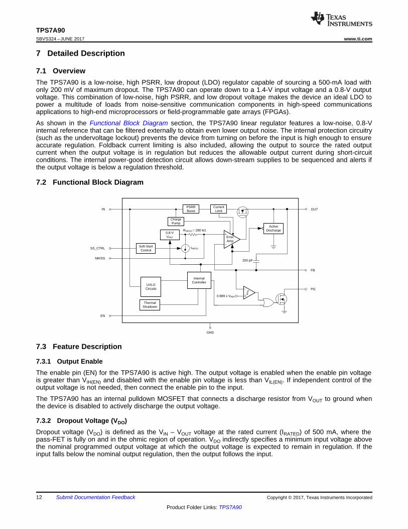
7.1 OverviewThe TPS7A90 is a low-noise, high PSRR, low dropout (LDO) regulator capable of sourcing a 500-mA load withonly 200 mV of maximum dropout. The TPS7A90 can operate down to a 1.4-V input voltage and a 0.8-V outputvoltage. This combination of low-noise, high PSRR, and low dropout voltage makes the device an ideal LDO topower a multitude of loads from noise-sensitive communication components in high-speed communicationsapplications to high-end microprocessors or field-programmable gate arrays (FPGAs).
As shown in the Functional Block Diagram section, the TPS7A90 linear regulator features a low-noise, 0.8-Vinternal reference that can be filtered externally to obtain even lower output noise. The internal protection circuitry(such as the undervoltage lockout) prevents the device from turning on before the input is high enough to ensureaccurate regulation. Foldback current limiting is also included, allowing the output to source the rated outputcurrent when the output voltage is in regulation but reduces the allowable output current during short-circuitconditions. The internal power-good detection circuit allows down-stream supplies to be sequenced and alerts ifthe output voltage is below a regulation threshold.
7.2 Functional Block Diagram
7.3 Feature Description
7.3.1 Output EnableThe enable pin (EN) for the TPS7A90 is active high. The output voltage is enabled when the enable pin voltageis greater than VIH(EN) and disabled with the enable pin voltage is less than VIL(EN). If independent control of theoutput voltage is not needed, then connect the enable pin to the input.
The TPS7A90 has an internal pulldown MOSFET that connects a discharge resistor from VOUT to ground whenthe device is disabled to actively discharge the output voltage.
7.3.2 Dropout Voltage (VDO)Dropout voltage (VDO) is defined as the VIN – VOUT voltage at the rated current (IRATED) of 500 mA, where thepass-FET is fully on and in the ohmic region of operation. VDO indirectly specifies a minimum input voltage abovethe nominal programmed output voltage at which the output voltage is expected to remain in regulation. If theinput falls below the nominal output regulation, then the output follows the input.

IN10
OUT
V (f )PSRR (dB) 20 Log
V (f )
§ · ¨ ¸
© ¹
R =DS(ON)
VDO
IRATED
13
TPS7A90www.ti.com SBVS324 –JUNE 2017
Product Folder Links: TPS7A90
Submit Documentation FeedbackCopyright © 2017, Texas Instruments Incorporated
Feature Description (continued)Dropout voltage is determined by the RDS(ON) of the pass-FET. Therefore, if the LDO operates below the ratedcurrent, then the VDO for that current scales accordingly. Use Equation 1 to calculate the RDS(ON) for theTPS7A90:
(1)
7.3.3 Output Voltage AccuracyOutput voltage accuracy specifies minimum and maximum output voltage error, relative to the expected nominaloutput voltage stated as a percent. The TPS7A90 features an output voltage accuracy of 1% that includes theerrors introduced by the internal reference, load regulation, and line regulation variance across the full range ofrated load and line operating conditions over temperature, as specified by the Electrical Characteristics table.Output voltage accuracy also accounts for all variations between manufacturing lots.
7.3.4 High Power-Supply Rejection Ratio (PSRR)PSRR is a measure of how well the LDO control loop rejects noise from the input source to make the dc outputvoltage as noise-free as possible across the frequency spectrum (usually measured from 10 Hz to 10 MHz).Even though PSRR is a loss in noise signal amplitude, the PSRR curves in the Typical Characteristics sectionare illustrated as positive values in decibels (dB) for convenience. Equation 2 gives the PSRR calculation as afunction of frequency where input noise voltage [VIN(f)] and output noise voltage [VOUT(f)] are the amplitudes ofthe respective sinusoidal signals.
(2)
Noise that couples from the input to the internal reference voltage is a primary contributor to reduced PSRRperformance. Using a noise-reduction capacitor is recommended to filter unwanted noise from the input voltage,which creates a low-pass filter with an internal resistor to improve PSRR performance at lower frequencies.
LDOs are often employed not only as a step-down regulators, but also to provide exceptionally clean power railsfor noise-sensitive components. This usage is especially true for the TPS7A90, which features an innovativecircuit to boost the PSRR between 200 kHz and 1 MHz. This boost circuit helps further filter switching noise fromswitching-regulators that operate in this region; see Figure 1. To achieve the maximum benefit of this PSRRboost circuit, using a capacitor with a minimum impedance in the 100-kHz to 1-MHz band is recommended.
7.3.5 Low Output NoiseLDO noise is defined as the internally-generated intrinsic noise created by the semiconductor circuits. TheTPS7A90 is designed for system applications where minimizing noise on the power-supply rail is critical tosystem performance. This scenario is the case for phase-locked loop (PLL)-based clocking circuits whereminimum phase noise is all important, or in test and measurement systems where even small power-supplynoise fluctuations can distort instantaneous measurement accuracy.
The TPS7A90 includes a low-noise reference ensuring minimal output noise in normal operation. Furtherimprovements can be made by adding a noise-reduction capacitor (CNR/SS), a feedforward capacitor (CFF), or acombination of the two. See the Noise-Reduction and Soft-Start Capacitor (CNR/SS) and Feed-Forward Capacitor(CFF) sections for additional design information.
For more information on noise and noise measurement, see the How to Measure LDO Noise white paper.
7.3.6 Output Soft-Start ControlSoft-start refers to the ramp-up characteristic of the output voltage during LDO turn-on after the EN and UVLOthresholds are exceeded. The noise-reduction capacitor (CNR/SS) serves a dual purpose of both governing outputnoise reduction and programming the soft-start ramp during turn-on. Larger values for the noise-reductioncapacitors decrease the noise but also result in a slower output turn-on ramp rate.
VREF
INR/SS
RNR
CNR/SS
GND
+
±
SW
VFB
NR/SS Control
14
TPS7A90SBVS324 –JUNE 2017 www.ti.com
Product Folder Links: TPS7A90
Submit Documentation Feedback Copyright © 2017, Texas Instruments Incorporated
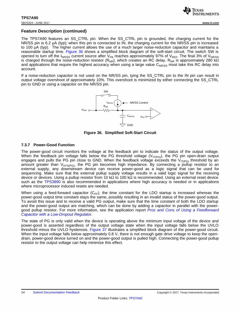
Feature Description (continued)The TPS7A90 features an SS_CTRL pin. When the SS_CTRL pin is grounded, the charging current for theNR/SS pin is 6.2 µA (typ); when this pin is connected to IN, the charging current for the NR/SS pin is increasedto 100 µA (typ). The higher current allows the use of a much larger noise-reduction capacitor and maintains areasonable startup time. Figure 36 shows a simplified block diagram of the soft-start circuit. The switch SW isopened to turn off the INR/SS current source after VFB reaches approximately 97% of VREF. The final 3% of VNR/SSis charged through the noise-reduction resistor (RNR), which creates an RC delay. RNR is approximately 280 kΩand applications that require the highest accuracy when using a large value CNR/SS must take this RC delay intoaccount.
If a noise-reduction capacitor is not used on the NR/SS pin, tying the SS_CTRL pin to the IN pin can result inoutput voltage overshoot of approximately 10%. This overshoot is minimized by either connecting the SS_CTRLpin to GND or using a capacitor on the NR/SS pin.
Figure 36. Simplified Soft-Start Circuit
7.3.7 Power-Good FunctionThe power-good circuit monitors the voltage at the feedback pin to indicate the status of the output voltage.When the feedback pin voltage falls below the PG threshold voltage (VIT(PG)), the PG pin open-drain outputengages and pulls the PG pin close to GND. When the feedback voltage exceeds the VIT(PG) threshold by anamount greater than VHYS(PG), the PG pin becomes high impedance. By connecting a pullup resistor to anexternal supply, any downstream device can receive power-good as a logic signal that can be used forsequencing. Make sure that the external pullup supply voltage results in a valid logic signal for the receivingdevice or devices. Using a pullup resistor from 10 kΩ to 100 kΩ is recommended. Using an external reset devicesuch as the TPS3890 is also recommended in applications where high accuracy is needed or in applicationswhere microprocessor induced resets are needed.
When using a feed-forward capacitor (CFF), the time constant for the LDO startup is increased whereas thepower-good output time constant stays the same, possibly resulting in an invalid status of the power-good output.To avoid this issue and to receive a valid PG output, make sure that the time constant of both the LDO startupand the power-good output are matching, which can be done by adding a capacitor in parallel with the power-good pullup resistor. For more information, see the application report Pros and Cons of Using a FeedforwardCapacitor with a Low-Dropout Regulator.
The state of PG is only valid when the device is operating above the minimum input voltage of the device andpower-good is asserted regardless of the output voltage state when the input voltage falls below the UVLOthreshold minus the UVLO hysteresis. Figure 37 illustrates a simplified block diagram of the power-good circuit.When the input voltage falls below approximately 0.8 V, there is not enough gate drive voltage to keep the open-drain, power-good device turned on and the power-good output is pulled high. Connecting the power-good pullupresistor to the output voltage can help minimize this effect.

GND
VREF
+
±
VIN
VFB
GND
VPG
ENGNDUVLO
15
TPS7A90www.ti.com SBVS324 –JUNE 2017
Product Folder Links: TPS7A90
Submit Documentation FeedbackCopyright © 2017, Texas Instruments Incorporated
Feature Description (continued)
Figure 37. Simplified PG Circuit
7.3.8 Internal Protection Circuitry
7.3.8.1 Undervoltage Lockout (UVLO)The TPS7A90 has an independent undervoltage lockout (UVLO) circuit that monitors the input voltage, allowinga controlled and consistent turn on and off of the output voltage. To prevent the device from turning off if theinput drops during turn on, the UVLO has approximately 290 mV of hysteresis.
The UVLO circuit responds quickly to glitches on VIN and disables the output of the device if this rail starts tocollapse too quickly. Use an input capacitor that is large enough to slow input transients to less then two voltsper microsecond.
7.3.8.2 Internal Current Limit (ICL)The internal current-limit circuit is used to protect the LDO against transient high-load current faults or shortingevents. The LDO is not designed to operate in current limit under steady-state conditions. During an overcurrentevent where the output voltage is pulled 10% below the regulated output voltage, the LDO sources a constantcurrent as specified in the Electrical Characteristics table. When the output voltage falls, the amount of outputcurrent is reduced to better protect the device. During a hard short-circuit event, the current is reduced toapproximately 1.45 A. See Figure 12 in the Typical Characteristics section for more information about thecurrent-limit foldback behavior. However, when a current-limit event occurs, the LDO begins to heat up becauseof the increase in power dissipation. The increase in heat can trigger the integrated thermal shutdown protectioncircuit.
7.3.8.3 Thermal ProtectionThe TPS7A90 contains a thermal shutdown protection circuit to turn off the output current when excessive heat isdissipated in the LDO. Thermal shutdown occurs when the thermal junction temperature (TJ) of the pass-FETexceeds 160°C (typical). Thermal shutdown hysteresis assures that the LDO again resets (turns on) when thetemperature falls to 140°C (typical). The thermal time-constant of the semiconductor die is fairly short, and thusthe output turns on and off at a high rate when thermal shutdown is reached until power dissipation is reduced.
The internal protection circuitry of the TPS7A90 is designed to protect against thermal overload conditions. Thecircuitry is not intended to replace proper heat sinking. Continuously running the TPS7A90 into thermal shutdowndegrades device reliability.
For reliable operation, limit junction temperature to a maximum of 125°C. To estimate the thermal margin in agiven layout, increase the ambient temperature until the thermal protection shutdown is triggered using worst-case load and highest input voltage conditions. For good reliability, thermal shutdown must occur at least 35°Cabove the maximum expected ambient temperature condition for the application. This configuration produces aworst-case junction temperature of 125°C at the highest expected ambient temperature and worst-case load.

16
TPS7A90SBVS324 –JUNE 2017 www.ti.com
Product Folder Links: TPS7A90
Submit Documentation Feedback Copyright © 2017, Texas Instruments Incorporated
(1) All table conditions must be met.(2) The device is disabled when any condition is met.
7.4 Device Functional ModesTable 1 provides a quick comparison between the normal, dropout, and disabled modes of operation.
Table 1. Device Functional Modes Comparison
OPERATING MODEPARAMETER
VIN EN IOUT TJ
Normal (1) VIN > VOUT(nom) + VDO VEN > VIH(EN) IOUT < ICL TJ < Tsd
Dropout (1) VIN < VOUT(nom) + VDO VEN > VIH(EN) IOUT < ICL TJ < Tsd
Disabled (2) VIN < VUVLO VEN < VIL(EN) — TJ > Tsd
7.4.1 Normal OperationThe device regulates to the nominal output voltage when all of the following conditions are met:• The input voltage is greater than the nominal output voltage plus the dropout voltage (VOUT(nom) + VDO)• The enable voltage has previously exceeded the enable rising threshold voltage and has not yet decreased
below the enable falling threshold• The output current is less than the current limit (IOUT < ICL)• The device junction temperature is less than the thermal shutdown temperature (TJ < Tsd)
7.4.2 Dropout OperationIf the input voltage is lower than the nominal output voltage plus the specified dropout voltage, but all otherconditions are met for normal operation, the device operates in dropout. In this mode, the output voltage tracksthe input voltage. During this mode, the transient performance of the device becomes significantly degradedbecause the pass device is in a triode state and no longer controls the current through the LDO. Line or loadtransients in dropout can result in large output-voltage deviations.
When the device is in a steady dropout state (defined as when the device is in dropout, VIN < VOUT(NOM) + VDO,right after being in a normal regulation state, but not during startup), the pass-FET is driven as hard as possible.When the input voltage returns to VIN ≥ VOUT(NOM) + VDO, VOUT can overshoot for a short period of time if the inputvoltage slew rate is greater than 0.1 V/µs.
7.4.3 DisabledThe output of the TPS7A90 can be shutdown by forcing the enable pin below 0.4 V. When disabled, the passdevice is turned off, internal circuits are shutdown, and the output voltage is actively discharged to ground by aninternal resistor from the output to ground.

REF(max)OUT1 2
REF 2
VVR = R 1 , where 5 A
V R
§ · ! P¨ ¸
© ¹
VOUTVIN OUTIN
EN
SS_CTRL
NR/SS
FBCIN COUT
CNR/SS
R1
R2
GNDPG
Copyright © 2016, Texas Instruments Incorporated
17
TPS7A90www.ti.com SBVS324 –JUNE 2017
Product Folder Links: TPS7A90
Submit Documentation FeedbackCopyright © 2017, Texas Instruments Incorporated
8 Application and Implementation
NOTEInformation in the following applications sections is not part of the TI componentspecification, and TI does not warrant its accuracy or completeness. TI’s customers areresponsible for determining suitability of components for their purposes. Customers shouldvalidate and test their design implementation to confirm system functionality.
8.1 Application InformationThe TPS7A90 is a linear voltage regulator operating from 1.4 V to 6.5 V on the input, and regulates voltagesbetween 0.8 V to 5.0 V within 1% accuracy and a 500-mA maximum output current. Efficiency is defined by theratio of output voltage to input voltage because the TPS7A90 is a linear voltage regulator. To achieve highefficiency, the dropout voltage (VIN – VOUT) must be as small as possible, thus requiring a very low dropout LDO.Successfully implementing an LDO in an application depends on the application requirements. This sectiondiscusses key device features and how to best implement them to achieve a reliable design.
8.1.1 Adjustable OutputAs Figure 38 shows, the output voltage of the TPS7A9001 can be adjusted from 0.8 V to 5.2 V by using aresistor divider network.
Figure 38. Adjustable Operation
Use Equation 3 to calculate R1 and R2 for any output voltage range. This resistive network must provide acurrent greater than or equal to 5 µA for optimum noise performance.
(3)
If greater voltage accuracy is required, take into account the output voltage offset contribution resulting from thefeedback pin current (IFB) and use 0.1%-tolerance resistors.

18
TPS7A90SBVS324 –JUNE 2017 www.ti.com
Product Folder Links: TPS7A90
Submit Documentation Feedback Copyright © 2017, Texas Instruments Incorporated
Application Information (continued)
(1) R1 is connected from OUT to FB; R2 is connected from FB to GND; see Figure 38.
Table 2 lists the resistor combination required to achieve a few of the most common rails using commercially-available, 0.1%-tolerance resistors to maximize nominal voltage accuracy and also abiding to the formula givenin Equation 3.
Table 2. Recommended Feedback-Resistor Values
VOUT(TARGET)(V)
FEEDBACK RESISTOR VALUES (1) CALCULATED OUTPUTVOLTAGE (V)R1 (kΩ) R2 (kΩ)
0.8 Short Open 0.8001.00 2.55 10.2 1.0001.20 5.9 11.8 1.2001.50 9.31 10.7 1.4961.80 1.87 1.5 1.7971.90 15.8 11.5 1.8992.50 2.43 1.15 2.4903.00 3.16 1.15 2.9983.30 3.57 1.15 3.2835.00 10.5 2 5.00
8.1.2 Start-Up
8.1.2.1 Enable (EN) and Undervoltage Lockout (UVLO)The TPS7A90 only turns on when EN and UVLO are above the respective voltage thresholds. The TPS7A90 hasan independent UVLO circuit that monitors the input voltage to allow a controlled and consistent turn on and off.The UVLO has approximately 290 mV of hysteresis to prevent the device from turning off if the input dropsduring turn on. The EN signal allows independent logic-level turn-on and shutdown of the LDO when the inputvoltage is present. Connecting EN directly to IN is recommended if independent turn-on is not needed.
The TPS7A90 has an internal pulldown MOSFET that connects a discharge resistor from VOUT to ground whenthe device is disabled to actively discharge the output voltage.
8.1.2.2 Noise-Reduction and Soft-Start Capacitor (CNR/SS)The CNR/SS capacitor serves a dual purpose of both reducing output noise and setting the soft-start ramp duringturn-on.
8.1.2.2.1 Noise Reduction
For low-noise applications, the CNR/SS capacitor forms an RC filter for filtering output noise that is otherwiseamplified by the control loop. For low-noise applications, a CNR/SS of between 10 nF to 10 µF is recommended.Larger values for CNR/SS can be used; however, above 1 µF there is little benefit in lowering the output voltagenoise for frequencies above 10 Hz.

OUT OUT OUTOUT
LOAD
C dV (t) V (t)I (t)
dt R
§ ·u§ · ¨ ¸¨ ¸© ¹ © ¹
19
TPS7A90www.ti.com SBVS324 –JUNE 2017
Product Folder Links: TPS7A90
Submit Documentation FeedbackCopyright © 2017, Texas Instruments Incorporated
8.1.2.2.2 Soft-Start and In-Rush Current
Soft-start refers to the gradual ramp-up characteristic of the output voltage after the EN and UVLO thresholds areexceeded. Reducing how quickly the output voltage increases during startup also reduces the amount of currentneeded to charge the output capacitor, referred to as in-rush current. In-rush current is defined as the currentgoing into the LDO during start-up. In-rush current consists of the load current, the current used to charge theoutput capacitor, and the ground pin current (that contributes very little to in-rush current). This current is difficultto measure because the input capacitor must be removed, which is not recommended. However, Equation 4 canbe used to estimate in-rush current:
where:• VOUT(t) is the instantaneous output voltage of the turn-on ramp• dVOUT(t) / dt is the slope of the VOUT ramp• RLOAD is the resistive load impedance (4)
The TPS7A90 features a monotonic, voltage-controlled soft-start that is set with an external capacitor (CNR/SS).This soft-start helps reduce in-rush current, minimizing load transients to the input power bus that can causepotential start-up initialization problems when powering FPGAs, digital signal processors (DSPs), or other highcurrent loads.
To achieve a monotonic start-up, the TPS7A90 error amplifier tracks the voltage ramp of the external soft-startcapacitor until the voltage exceeds approximately 97% of the internal reference. The final 3% of VNR/SS ischarged through the noise-reduction resistor (RNR), creating an RC delay. RNR is approximately 280 kΩ andapplications that require the highest accuracy when using a large value CNR/SS must take this RC delay intoaccount.
The soft-start ramp time depends on the soft-start charging current (INR/SS), the soft-start capacitance (CNR/SS),and the internal reference (VREF). Use Equation 5 to calculate the approximate soft-start ramp time (tSS):
tSS = (VREF × CNR/SS) / INR/SS (5)
The value for INR/SS is determined by the state of the SS_CTRL pin. When the SS_CTRL pin is connected toGND, the typical value for the INR/SS current is 6.2 µA. Connecting the SS_CTRL pin to IN increases the typicalsoft-start charging current to 100 µA. The larger charging current for INR/SS is useful if shorter start-up times areneeded (such as when using a large noise-reduction capacitor).
8.1.3 Capacitor RecommendationThe TPS7A90 is designed to be stable using low equivalent series resistance (ESR) ceramic capacitors at theinput, output, and noise-reduction pin. Multilayer ceramic capacitors are the industry standard for these types ofapplications and are recommended, but must be used with good understanding of their limitations. Ceramiccapacitors that employ X7R-, X5R-, and COG-rated dielectric materials provide relatively good capacitive stabilityacross temperature, whereas the use of Y5V-rated capacitors is discouraged precisely because the capacitancevaries so widely. In all cases, ceramic capacitors vary a great deal with operating voltage and temperature andthe design engineer must be aware of these characteristics. As a rule of thumb, ceramic capacitors arerecommended to be derated by 50%. The input and output capacitors recommended herein account for acapacitance derating of 50%.

T = T + ( PJ A JA Dq ´ )
20
TPS7A90SBVS324 –JUNE 2017 www.ti.com
Product Folder Links: TPS7A90
Submit Documentation Feedback Copyright © 2017, Texas Instruments Incorporated
8.1.3.1 Input and Output Capacitor Requirements (CIN and COUT)The TPS7A90 is designed and characterized for operation with ceramic capacitors of 10 µF or greater at theinput and output. Locate the input and output capacitors as near as practical to the input and output pins tominimize the trace inductance from the capacitor to the device.
Attention must be given to the input capacitance to minimize transient input droop during startup and load currentsteps. Simply using very large ceramic input capacitances can cause unwanted ringing at the output if the inputcapacitor (in combination with the wire-lead inductance) creates a high-Q peaking effect during transients, whichis why short, well-designed interconnect traces to the upstream supply are needed to minimize ringing. Dampingof unwanted ringing can be accomplished by using a tantalum capacitor, with a few hundred milliohms of ESR, inparallel with the ceramic input capacitor. The UVLO circuit responds quickly to glitches on VIN and disables theoutput of the device if this rail starts to collapse too quickly. Use an input capacitor that is large enough to slowinput transients to less then two volts per microsecond.
8.1.3.1.1 Load-Step Transient Response
The load-step transient response is the output voltage response by the LDO to a step change in load current.The depth of charge depletion immediately after the load step is directly proportional to the amount of outputcapacitance. However, although larger output capacitances decrease any voltage dip or peak occurring during aload step, the control-loop bandwidth is also decreased, thereby slowing the response time.
The LDO cannot sink charge, therefore when the output load is removed or greatly reduced, the control loopmust turn off the pass-FET and wait for any excess charge to deplete.
8.1.3.2 Feed-Forward Capacitor (CFF)Although a feed-forward capacitor (CFF), from the FB pin to the OUT pin is not required to achieve stability, a10-nF, feed-forward capacitor improves the noise and PSRR performance. A higher capacitance CFF can beused; however, the startup time is longer and the power-good signal can incorrectly indicate that the outputvoltage has settled. For a detailed description, see the application report Pros and Cons of Using a FeedforwardCapacitor with a Low-Dropout Regulator.
8.1.4 Power Dissipation (PD)Circuit reliability demands that proper consideration be given to device power dissipation, location of the circuiton the printed circuit board (PCB), and correct sizing of the thermal plane. The PCB area around the regulatormust be as free as possible of other heat-generating devices that cause added thermal stresses.
To a first-order approximation, power dissipation in the regulator depends on the input-to-output voltagedifference and load conditions. Equation 6 calculates PD:
PD = (VIN – VOUT) × IOUT (6)
Power dissipation can be minimized, and thus greater efficiency achieved, by proper selection of the systemvoltage rails. For the lowest power dissipation use the minimum input voltage necessary for proper outputregulation.
The primary heat conduction path for the DSK package is through the thermal pad to the PCB. Solder thethermal pad to a copper pad area under the device. This pad area should contain an array of plated vias thatconduct heat to additional copper planes for increased heat dissipation.
The maximum power dissipation determines the maximum allowable ambient temperature (TA) for the device.According to Equation 7, power dissipation and junction temperature are most often related by the junction-to-ambient thermal resistance (θJA) of the combined PCB and device package and the temperature of the ambientair (TA).
(7)
Unfortunately, the thermal resistance (θJA) is highly dependent on the heat-spreading capability built into theparticular PCB design, and therefore varies according to the total copper area, copper weight, and location of theplanes. The θJA recorded in the Thermal Information table is determined by the JEDEC standard, PCB, andcopper-spreading area and is only used as a relative measure of package thermal performance.

1.2 V2.0 V OUT
PG
IN
EN
TPS7A90
SS_CTRL
NR/SS
FBCIN
10 PFCOUT
10 F
CNR/SS
0.1 PF
R1
R2
11.8 k:
5.9 k:
VOUT
RPG
20 k:PG
GND
CFF 10 nF
Copyright © 2017, Texas Instruments Incorporated
Y
Y Y ´
JT J T JT D: T = T + PY ´
JB J B JB D: T = T + P
21
TPS7A90www.ti.com SBVS324 –JUNE 2017
Product Folder Links: TPS7A90
Submit Documentation FeedbackCopyright © 2017, Texas Instruments Incorporated
8.1.5 Estimating Junction TemperatureThe JEDEC standard recommends the use of psi (Ψ) thermal metrics to estimate the junction temperatures ofthe LDO when in-circuit on a typical PCB board application. These metrics are not strictly speaking thermalresistances, but rather offer practical and relative means of estimating junction temperatures. These psi metricsare determined to be significantly independent of the copper-spreading area. The key thermal metrics (ΨJT andΨJB) are used in accordance with Equation 8 and are given in the Thermal Information table.
where:• PD is the power dissipated as explained in Equation 6• TT is the temperature at the center-top of the device package• TB is the PCB surface temperature measured 1 mm from the device package and centered on the package
edge (8)
For a more detailed discussion on thermal metrics and how to use them, see the application reportSemiconductor and IC Package Thermal Metrics.
8.2 Typical ApplicationThis section discusses the implementation of the TPS7A90 to regulate from a 2-V input voltage to a 1.2-V outputvoltage for noise-sensitive loads. Figure 39 shows the schematic for this application circuit.
Figure 39. Application Example
8.2.1 Design RequirementsFor the design example shown in Figure 39, use the parameters listed in Table 3 as the input parameters.
Table 3. Design ParametersPARAMETER APPLICATION REQUIREMENTS DESIGN RESULTS
Input voltages (VIN) 2 V, ±3%, provided by the dc-dc converterswitching at 750 kHz 1.4 V to 6.5 V
Maximum ambient operatingtemperature 85°C 108°C junction temperature
Output voltages (VOUT) 1.2 V, ±1% 1.2 V, ±1%Output currents (IOUT) 500 mA (max), 10 mA (min) 500 mA (max), 5 mA (min)
RMS noise < 6 µVRMS, bandwidth = 10 Hz to 100 kHz 5.2 µVRMS, bandwidth = 10 Hz to 100 kHzPSRR at 500 kHz > 40 dB 47 dB
Startup time < 2 ms 80 µs (typ) 148 µs (max)

Frequency (Hz)
Pow
er-S
uppl
y R
ejec
tion
Rat
io (
dB)
0
10
20
30
40
50
60
70
10 100 1k 10k 100k 1M 10M
VIN2.0 V
Frequency (Hz)
Noi
se (PV
Hz)
0.001
0.01
0.1
1
10
10 100 1k 10k 100k 1M 10M
5.2 PVRMSCNR = 10 nF, CFF = 10 nF
22
TPS7A90SBVS324 –JUNE 2017 www.ti.com
Product Folder Links: TPS7A90
Submit Documentation Feedback Copyright © 2017, Texas Instruments Incorporated
8.2.2 Detailed Design ProcedureThe output voltage can be set to 1.2 V by selecting the correct values for R1 and R2; see Equation 3.
Input and output capacitors are selected in accordance with the Capacitor Recommendation section. Ceramiccapacitances of 10 µF for both input and output are selected to help balance the charge needed during startupwhen charging the output capacitor, thus reducing the input voltage drop.
To satisfy the required startup time (tSS) and still maintain low-noise performance, a 0.01-µF CNR/SS is selectedfor with SS_CTRL connected to VIN. Equation 9 calculates this value. Using INR/SS(MAX) and the smallest CNR/SScapacitance resulting from manufacturing variance (often ±20%) provides the fastest startup time, whereas usingINR/SS(MIN) and the largest CNR/SS capacitance resulting from manufacturing variance provides the slowest startuptime.
tSS = (VREF × CNR/SS) / INR/SS (9)
With a 500-mA maximum load, the internal power dissipation is 800 mW, corresponding to a 23°C junctiontemperature rise. With an 85°C maximum ambient temperature, the junction temperature is at 108°C. Tominimize noise, a feed-forward capacitance (CFF) of 10 nF is selected.
See the Layout section for an example of how to layout the TPS7A90 to achieve best PSRR and noise.
8.2.3 Application Curves
Figure 40. PSRR vs Frequency Figure 41. Output Noise vs Frequency
9 Power Supply RecommendationsThe input of the TPS7A90 is designed to operate from an input voltage range between 1.4 V and 6.5 V and withan input capacitor of 10 µF. The input voltage range must provide adequate headroom in order for the device tohave a regulated output. This input supply must be well regulated. If the input supply is noisy, additional inputcapacitors can be used to improve the output noise performance.
10 Layout
10.1 Layout GuidelinesGeneral guidelines for linear regulator designs are to place all circuit components on the same side of the circuitboard and as near as practical to the respective LDO pin connections. Place ground return connections to theinput and output capacitors, and to the LDO ground pin as close to each other as possible, connected by a wide,component-side, copper surface. The use of vias and long traces to create LDO circuit connections is stronglydiscouraged and negatively affects system performance.

OUT
EN
IN
NR/SSFB
SS_CTRL
INOUT
GND
1
5
2
4
3
10
6
9
7
8
CINCOUT
CNR/SS
R1
Ground Plane for
Thermal Relief and
Signal Ground
VINVOUT
PG
R2
CFF
To PG
Pullup Supply
PG Output
To VIN
Power Ground
Plane
Denotes vias used for application purposes
23
TPS7A90www.ti.com SBVS324 –JUNE 2017
Product Folder Links: TPS7A90
Submit Documentation FeedbackCopyright © 2017, Texas Instruments Incorporated
Layout Guidelines (continued)10.1.1 Board LayoutTo maximize the ac performance of the TPS7A90, following the layout example shown in Figure 42 isrecommended. This layout isolates the analog ground (AGND) from the noisy power ground. Components thatmust be connected to the quiet analog ground are the noise-reduction capacitor (CNR/SS) and the lower feedbackresistor (R2). These components must have a separate connection back to the thermal pad of the device foroptimal output noise performance. Connect the GND pin directly to the thermal pad and not to any externalplane.
To maximize the output voltage accuracy, the connection from the output voltage back to top output dividerresistors (R1) must be made as close as possible to the load. This method of connecting the feedback traceeliminates the voltage drop from the device output to the load.
To improve thermal performance, use an array of thermal vias to connect the thermal pad to the ground planes.Larger ground planes improve the thermal performance of the device and lowering the operating temperature ofthe device.
10.2 Layout Example
Figure 42. TPS7A90 Example Layout

24
TPS7A90SBVS324 –JUNE 2017 www.ti.com
Product Folder Links: TPS7A90
Submit Documentation Feedback Copyright © 2017, Texas Instruments Incorporated
(1) For the most current package and ordering information see the Package Option Addendum at the end of this document, or see thedevice product folder at www.ti.com.
11 Device and Documentation Support
11.1 Device Support
11.1.1 Development Support
11.1.1.1 Evaluation ModulesAn evaluation module (EVM) is available to assist in the initial circuit performance evaluation using the TPS7A90.Table 4 shows the summary information for this fixture.
Table 4. Design Kits and Evaluation Modules (1)
NAME PART NUMBERTPS7A90EVM-831 Evaluation Module User's Guide TPS7A90EVM-831
(1) For the most current package and ordering information see the Package Option Addendum at the end of this document, or see thedevice product folder at www.ti.com.
The EVM can be requested at the Texas Instruments web site through the TPS7A90 product folder.
11.1.1.2 SPICE ModelsComputer simulation of circuit performance using SPICE is often useful when analyzing the performance ofanalog circuits and systems. A SPICE model for the TPS7A90 is available through the TPS7A90 product folderunder simulation models.
11.1.2 Device Nomenclature
Table 5. Ordering Information (1)
PRODUCT DESCRIPTION
TPS7A90XXYYYZXX represents the output voltage. 01 is the adjustable output version.YYY is the package designator.Z is the package quantity.
11.2 Documentation Support
11.2.1 Related DocumentationFor related documentation see the following:• TPS3890 Low Quiescent Current, 1% Accurate Supervisor with Programmable Delay• TPS7A90EVM-831 Evaluation Module User's Guide• How to Measure LDO Noise• Pros and Cons of Using a Feedforward Capacitor with a Low-Dropout Regulator• Semiconductor and IC Package Thermal Metrics
11.3 Receiving Notification of Documentation UpdatesTo receive notification of documentation updates, navigate to the device product folder on ti.com. In the upperright corner, click on Alert me to register and receive a weekly digest of any product information that haschanged. For change details, review the revision history included in any revised document.

25
TPS7A90www.ti.com SBVS324 –JUNE 2017
Product Folder Links: TPS7A90
Submit Documentation FeedbackCopyright © 2017, Texas Instruments Incorporated
11.4 Community ResourcesThe following links connect to TI community resources. Linked contents are provided "AS IS" by the respectivecontributors. They do not constitute TI specifications and do not necessarily reflect TI's views; see TI's Terms ofUse.
TI E2E™ Online Community TI's Engineer-to-Engineer (E2E) Community. Created to foster collaborationamong engineers. At e2e.ti.com, you can ask questions, share knowledge, explore ideas and helpsolve problems with fellow engineers.
Design Support TI's Design Support Quickly find helpful E2E forums along with design support tools andcontact information for technical support.
11.5 TrademarksE2E is a trademark of Texas Instruments.All other trademarks are the property of their respective owners.
11.6 Electrostatic Discharge CautionThis integrated circuit can be damaged by ESD. Texas Instruments recommends that all integrated circuits be handled withappropriate precautions. Failure to observe proper handling and installation procedures can cause damage.
ESD damage can range from subtle performance degradation to complete device failure. Precision integrated circuits may be moresusceptible to damage because very small parametric changes could cause the device not to meet its published specifications.
11.7 GlossarySLYZ022 — TI Glossary.
This glossary lists and explains terms, acronyms, and definitions.
12 Mechanical, Packaging, and Orderable InformationThe following pages include mechanical, packaging, and orderable information. This information is the mostcurrent data available for the designated devices. This data is subject to change without notice and revision ofthis document. For browser-based versions of this data sheet, refer to the left-hand navigation.

PACKAGE OPTION ADDENDUM
www.ti.com 1-Jul-2017
Addendum-Page 1
PACKAGING INFORMATION
Orderable Device Status(1)
Package Type PackageDrawing
Pins PackageQty
Eco Plan(2)
Lead/Ball Finish(6)
MSL Peak Temp(3)
Op Temp (°C) Device Marking(4/5)
Samples
TPS7A9001DSKR ACTIVE SON DSK 10 3000 Green (RoHS& no Sb/Br)
CU NIPDAU Level-2-260C-1 YEAR -40 to 125 1CEP
TPS7A9001DSKT ACTIVE SON DSK 10 250 Green (RoHS& no Sb/Br)
CU NIPDAU Level-2-260C-1 YEAR -40 to 125 1CEP
(1) The marketing status values are defined as follows:ACTIVE: Product device recommended for new designs.LIFEBUY: TI has announced that the device will be discontinued, and a lifetime-buy period is in effect.NRND: Not recommended for new designs. Device is in production to support existing customers, but TI does not recommend using this part in a new design.PREVIEW: Device has been announced but is not in production. Samples may or may not be available.OBSOLETE: TI has discontinued the production of the device.
(2) RoHS: TI defines "RoHS" to mean semiconductor products that are compliant with the current EU RoHS requirements for all 10 RoHS substances, including the requirement that RoHS substancedo not exceed 0.1% by weight in homogeneous materials. Where designed to be soldered at high temperatures, "RoHS" products are suitable for use in specified lead-free processes. TI mayreference these types of products as "Pb-Free".RoHS Exempt: TI defines "RoHS Exempt" to mean products that contain lead but are compliant with EU RoHS pursuant to a specific EU RoHS exemption.Green: TI defines "Green" to mean the content of Chlorine (Cl) and Bromine (Br) based flame retardants meet JS709B low halogen requirements of <=1000ppm threshold. Antimony trioxide basedflame retardants must also meet the <=1000ppm threshold requirement.
(3) MSL, Peak Temp. - The Moisture Sensitivity Level rating according to the JEDEC industry standard classifications, and peak solder temperature.
(4) There may be additional marking, which relates to the logo, the lot trace code information, or the environmental category on the device.
(5) Multiple Device Markings will be inside parentheses. Only one Device Marking contained in parentheses and separated by a "~" will appear on a device. If a line is indented then it is a continuationof the previous line and the two combined represent the entire Device Marking for that device.
(6) Lead/Ball Finish - Orderable Devices may have multiple material finish options. Finish options are separated by a vertical ruled line. Lead/Ball Finish values may wrap to two lines if the finishvalue exceeds the maximum column width.
Important Information and Disclaimer:The information provided on this page represents TI's knowledge and belief as of the date that it is provided. TI bases its knowledge and belief on informationprovided by third parties, and makes no representation or warranty as to the accuracy of such information. Efforts are underway to better integrate information from third parties. TI has taken andcontinues to take reasonable steps to provide representative and accurate information but may not have conducted destructive testing or chemical analysis on incoming materials and chemicals.TI and TI suppliers consider certain information to be proprietary, and thus CAS numbers and other limited information may not be available for release.
In no event shall TI's liability arising out of such information exceed the total purchase price of the TI part(s) at issue in this document sold by TI to Customer on an annual basis.

PACKAGE OPTION ADDENDUM
www.ti.com 1-Jul-2017
Addendum-Page 2

TAPE AND REEL INFORMATION
*All dimensions are nominal
Device PackageType
PackageDrawing
Pins SPQ ReelDiameter
(mm)
ReelWidth
W1 (mm)
A0(mm)
B0(mm)
K0(mm)
P1(mm)
W(mm)
Pin1Quadrant
TPS7A9001DSKR SON DSK 10 3000 178.0 8.4 2.75 2.75 0.95 4.0 8.0 Q2
TPS7A9001DSKT SON DSK 10 250 178.0 8.4 2.75 2.75 0.95 4.0 8.0 Q2
PACKAGE MATERIALS INFORMATION
www.ti.com 29-Jun-2017
Pack Materials-Page 1

*All dimensions are nominal
Device Package Type Package Drawing Pins SPQ Length (mm) Width (mm) Height (mm)
TPS7A9001DSKR SON DSK 10 3000 205.0 200.0 33.0
TPS7A9001DSKT SON DSK 10 250 205.0 200.0 33.0
PACKAGE MATERIALS INFORMATION
www.ti.com 29-Jun-2017
Pack Materials-Page 2


IMPORTANT NOTICE
Texas Instruments Incorporated (TI) reserves the right to make corrections, enhancements, improvements and other changes to itssemiconductor products and services per JESD46, latest issue, and to discontinue any product or service per JESD48, latest issue. Buyersshould obtain the latest relevant information before placing orders and should verify that such information is current and complete.TI’s published terms of sale for semiconductor products (http://www.ti.com/sc/docs/stdterms.htm) apply to the sale of packaged integratedcircuit products that TI has qualified and released to market. Additional terms may apply to the use or sale of other types of TI products andservices.Reproduction of significant portions of TI information in TI data sheets is permissible only if reproduction is without alteration and isaccompanied by all associated warranties, conditions, limitations, and notices. TI is not responsible or liable for such reproduceddocumentation. Information of third parties may be subject to additional restrictions. Resale of TI products or services with statementsdifferent from or beyond the parameters stated by TI for that product or service voids all express and any implied warranties for theassociated TI product or service and is an unfair and deceptive business practice. TI is not responsible or liable for any such statements.Buyers and others who are developing systems that incorporate TI products (collectively, “Designers”) understand and agree that Designersremain responsible for using their independent analysis, evaluation and judgment in designing their applications and that Designers havefull and exclusive responsibility to assure the safety of Designers' applications and compliance of their applications (and of all TI productsused in or for Designers’ applications) with all applicable regulations, laws and other applicable requirements. Designer represents that, withrespect to their applications, Designer has all the necessary expertise to create and implement safeguards that (1) anticipate dangerousconsequences of failures, (2) monitor failures and their consequences, and (3) lessen the likelihood of failures that might cause harm andtake appropriate actions. Designer agrees that prior to using or distributing any applications that include TI products, Designer willthoroughly test such applications and the functionality of such TI products as used in such applications.TI’s provision of technical, application or other design advice, quality characterization, reliability data or other services or information,including, but not limited to, reference designs and materials relating to evaluation modules, (collectively, “TI Resources”) are intended toassist designers who are developing applications that incorporate TI products; by downloading, accessing or using TI Resources in anyway, Designer (individually or, if Designer is acting on behalf of a company, Designer’s company) agrees to use any particular TI Resourcesolely for this purpose and subject to the terms of this Notice.TI’s provision of TI Resources does not expand or otherwise alter TI’s applicable published warranties or warranty disclaimers for TIproducts, and no additional obligations or liabilities arise from TI providing such TI Resources. TI reserves the right to make corrections,enhancements, improvements and other changes to its TI Resources. TI has not conducted any testing other than that specificallydescribed in the published documentation for a particular TI Resource.Designer is authorized to use, copy and modify any individual TI Resource only in connection with the development of applications thatinclude the TI product(s) identified in such TI Resource. NO OTHER LICENSE, EXPRESS OR IMPLIED, BY ESTOPPEL OR OTHERWISETO ANY OTHER TI INTELLECTUAL PROPERTY RIGHT, AND NO LICENSE TO ANY TECHNOLOGY OR INTELLECTUAL PROPERTYRIGHT OF TI OR ANY THIRD PARTY IS GRANTED HEREIN, including but not limited to any patent right, copyright, mask work right, orother intellectual property right relating to any combination, machine, or process in which TI products or services are used. Informationregarding or referencing third-party products or services does not constitute a license to use such products or services, or a warranty orendorsement thereof. Use of TI Resources may require a license from a third party under the patents or other intellectual property of thethird party, or a license from TI under the patents or other intellectual property of TI.TI RESOURCES ARE PROVIDED “AS IS” AND WITH ALL FAULTS. TI DISCLAIMS ALL OTHER WARRANTIES ORREPRESENTATIONS, EXPRESS OR IMPLIED, REGARDING RESOURCES OR USE THEREOF, INCLUDING BUT NOT LIMITED TOACCURACY OR COMPLETENESS, TITLE, ANY EPIDEMIC FAILURE WARRANTY AND ANY IMPLIED WARRANTIES OFMERCHANTABILITY, FITNESS FOR A PARTICULAR PURPOSE, AND NON-INFRINGEMENT OF ANY THIRD PARTY INTELLECTUALPROPERTY RIGHTS. TI SHALL NOT BE LIABLE FOR AND SHALL NOT DEFEND OR INDEMNIFY DESIGNER AGAINST ANY CLAIM,INCLUDING BUT NOT LIMITED TO ANY INFRINGEMENT CLAIM THAT RELATES TO OR IS BASED ON ANY COMBINATION OFPRODUCTS EVEN IF DESCRIBED IN TI RESOURCES OR OTHERWISE. IN NO EVENT SHALL TI BE LIABLE FOR ANY ACTUAL,DIRECT, SPECIAL, COLLATERAL, INDIRECT, PUNITIVE, INCIDENTAL, CONSEQUENTIAL OR EXEMPLARY DAMAGES INCONNECTION WITH OR ARISING OUT OF TI RESOURCES OR USE THEREOF, AND REGARDLESS OF WHETHER TI HAS BEENADVISED OF THE POSSIBILITY OF SUCH DAMAGES.Unless TI has explicitly designated an individual product as meeting the requirements of a particular industry standard (e.g., ISO/TS 16949and ISO 26262), TI is not responsible for any failure to meet such industry standard requirements.Where TI specifically promotes products as facilitating functional safety or as compliant with industry functional safety standards, suchproducts are intended to help enable customers to design and create their own applications that meet applicable functional safety standardsand requirements. Using products in an application does not by itself establish any safety features in the application. Designers mustensure compliance with safety-related requirements and standards applicable to their applications. Designer may not use any TI products inlife-critical medical equipment unless authorized officers of the parties have executed a special contract specifically governing such use.Life-critical medical equipment is medical equipment where failure of such equipment would cause serious bodily injury or death (e.g., lifesupport, pacemakers, defibrillators, heart pumps, neurostimulators, and implantables). Such equipment includes, without limitation, allmedical devices identified by the U.S. Food and Drug Administration as Class III devices and equivalent classifications outside the U.S.TI may expressly designate certain products as completing a particular qualification (e.g., Q100, Military Grade, or Enhanced Product).Designers agree that it has the necessary expertise to select the product with the appropriate qualification designation for their applicationsand that proper product selection is at Designers’ own risk. Designers are solely responsible for compliance with all legal and regulatoryrequirements in connection with such selection.Designer will fully indemnify TI and its representatives against any damages, costs, losses, and/or liabilities arising out of Designer’s non-compliance with the terms and provisions of this Notice.
Mailing Address: Texas Instruments, Post Office Box 655303, Dallas, Texas 75265Copyright © 2017, Texas Instruments Incorporated