tps61194-q1 datasheet - texas instruments · – central information displays (cid) – audio-video...
TRANSCRIPT
TPS61194-Q1
FB
PWM
OUT1
OUT2
OUT3
L1 D1 VOUT up to 45 VVIN 4.5...40 V
COUTCIN
RISET
Up to 100 mA/string
SW
LDO
FSET
VDDIO/EN
SYNC
PGND GND PAD
VIN
ISETFAULT
EN
BRIGHTNESS
RFSET
CLDO
OUT4
R1R2
CFB
Copyright © 2016, Texas Instruments Incorporated
65
70
75
80
85
90
95
100
0 20 40 60 80 100
Sys
tem
effi
cien
cy (
%)
Brightness (%)
VIN=5V
VIN=8V
VIN=12V
VIN=16V
C012
Product
Folder
Order
Now
Technical
Documents
Tools &
Software
Support &Community
An IMPORTANT NOTICE at the end of this data sheet addresses availability, warranty, changes, use in safety-critical applications,intellectual property matters and other important disclaimers. PRODUCTION DATA.
TPS61194-Q1SNVSAE9D –JANUARY 2016–REVISED MAY 2017
TPS61194-Q1 Low-EMI Automotive LED Driver With Four 100-mA Channels
1
1 Features1• Qualified for Automotive Applications• AEC-Q100 Qualified With the Following Results:
– Device Temperature Grade 1: –40°C to+125°C Ambient Operating TemperatureRange
• Input Voltage Operating Range 4.5 V to 40 V• Four High-Precision Current Sinks
– Current Matching 1% (Typical)– LED String Current up to 100 mA per Channel– Outputs can be Combined Externally for
Higher Current per String• High Dimming Ratio of 10 000:1 at 100 Hz• Integrated Boost/SEPIC Converter for LED String
Power– Output Voltage up to 45 V– Switching Frequency 300 kHz to 2.2 MHz– Switching Synchronization Input– Spread Spectrum for Lower EMI
• Extensive Fault Detection Features– Fault Output– Input Voltage OVP and UVLO– Open and Shorted LED Fault Detection– Thermal Shutdown
• Minimum Number of External Components
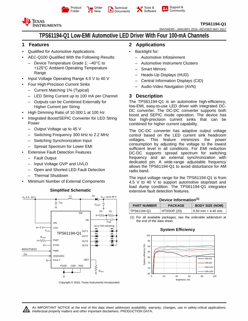
Simplified Schematic
2 Applications• Backlight for:
– Automotive Infotainment– Automotive Instrument Clusters– Smart Mirrors– Heads-Up Displays (HUD)– Central Information Displays (CID)– Audio-Video Navigation (AVN)
3 DescriptionThe TPS61194-Q1 is an automotive high-efficiency,low-EMI, easy-to-use LED driver with integrated DC-DC converter. The DC-DC converter supports bothboost and SEPIC mode operation. The device hasfour high-precision current sinks that can becombined for higher current capability.
The DC-DC converter has adaptive output voltagecontrol based on the LED current sink headroomvoltages. This feature minimizes the powerconsumption by adjusting the voltage to the lowestsufficient level in all conditions. For EMI reductionDC-DC supports spread spectrum for switchingfrequency and an external synchronization withdedicated pin. A wide-range adjustable frequencyallows the TPS61194-Q1 to avoid disturbance for AMradio band.
The input voltage range for the TPS61194-Q1 is from4.5 V to 40 V to support automotive stop/start andload dump condition. The TPS61194-Q1 integratesextensive fault detection features.
Device Information(1)
PART NUMBER PACKAGE BODY SIZE (NOM)TPS61194-Q1 HTSSOP (20) 6.50 mm × 4.40 mm
(1) For all available packages, see the orderable addendum atthe end of the data sheet.
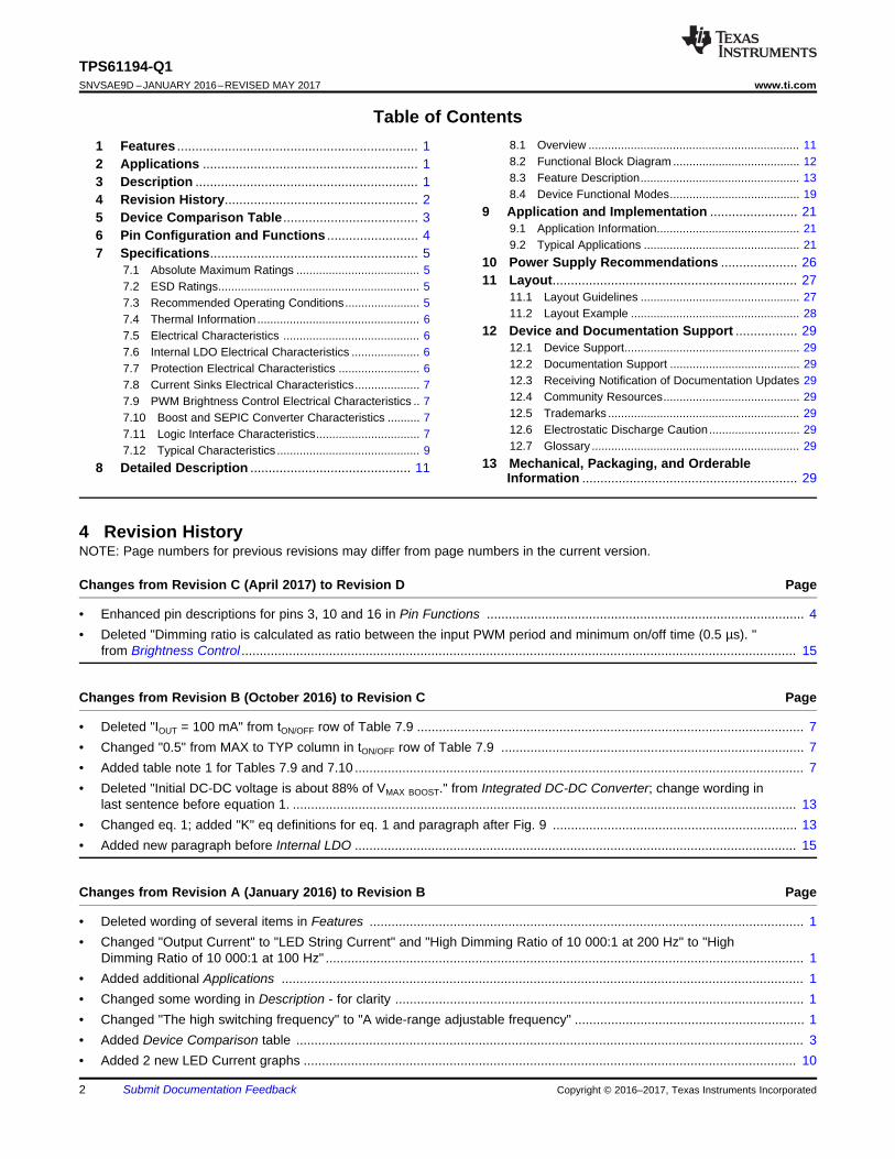
System Efficiency
2
TPS61194-Q1SNVSAE9D –JANUARY 2016–REVISED MAY 2017 www.ti.com
Submit Documentation Feedback Copyright © 2016–2017, Texas Instruments Incorporated
Table of Contents1 Features .................................................................. 12 Applications ........................................................... 13 Description ............................................................. 14 Revision History..................................................... 25 Device Comparison Table ..................................... 36 Pin Configuration and Functions ......................... 47 Specifications......................................................... 5
7.1 Absolute Maximum Ratings ...................................... 57.2 ESD Ratings.............................................................. 57.3 Recommended Operating Conditions....................... 57.4 Thermal Information .................................................. 67.5 Electrical Characteristics .......................................... 67.6 Internal LDO Electrical Characteristics ..................... 67.7 Protection Electrical Characteristics ......................... 67.8 Current Sinks Electrical Characteristics.................... 77.9 PWM Brightness Control Electrical Characteristics .. 77.10 Boost and SEPIC Converter Characteristics .......... 77.11 Logic Interface Characteristics................................ 77.12 Typical Characteristics ............................................ 9
8 Detailed Description ............................................ 11
8.1 Overview ................................................................. 118.2 Functional Block Diagram ....................................... 128.3 Feature Description................................................. 138.4 Device Functional Modes........................................ 19
9 Application and Implementation ........................ 219.1 Application Information............................................ 219.2 Typical Applications ................................................ 21
10 Power Supply Recommendations ..................... 2611 Layout................................................................... 27
11.1 Layout Guidelines ................................................. 2711.2 Layout Example .................................................... 28
12 Device and Documentation Support ................. 2912.1 Device Support...................................................... 2912.2 Documentation Support ........................................ 2912.3 Receiving Notification of Documentation Updates 2912.4 Community Resources.......................................... 2912.5 Trademarks ........................................................... 2912.6 Electrostatic Discharge Caution............................ 2912.7 Glossary ................................................................ 29
13 Mechanical, Packaging, and OrderableInformation ........................................................... 29
4 Revision HistoryNOTE: Page numbers for previous revisions may differ from page numbers in the current version.
Changes from Revision C (April 2017) to Revision D Page
• Enhanced pin descriptions for pins 3, 10 and 16 in Pin Functions ....................................................................................... 4• Deleted "Dimming ratio is calculated as ratio between the input PWM period and minimum on/off time (0.5 µs). "
from Brightness Control ........................................................................................................................................................ 15
Changes from Revision B (October 2016) to Revision C Page
• Deleted "IOUT = 100 mA" from tON/OFF row of Table 7.9 .......................................................................................................... 7• Changed "0.5" from MAX to TYP column in tON/OFF row of Table 7.9 ................................................................................... 7• Added table note 1 for Tables 7.9 and 7.10 ........................................................................................................................... 7• Deleted "Initial DC-DC voltage is about 88% of VMAX BOOST." from Integrated DC-DC Converter; change wording in
last sentence before equation 1. .......................................................................................................................................... 13• Changed eq. 1; added "K" eq definitions for eq. 1 and paragraph after Fig. 9 ................................................................... 13• Added new paragraph before Internal LDO ......................................................................................................................... 15
Changes from Revision A (January 2016) to Revision B Page
• Deleted wording of several items in Features ....................................................................................................................... 1• Changed "Output Current" to "LED String Current" and "High Dimming Ratio of 10 000:1 at 200 Hz" to "High
Dimming Ratio of 10 000:1 at 100 Hz" ................................................................................................................................... 1• Added additional Applications ............................................................................................................................................... 1• Changed some wording in Description - for clarity ................................................................................................................ 1• Changed "The high switching frequency" to "A wide-range adjustable frequency" ............................................................... 1• Added Device Comparison table ........................................................................................................................................... 3• Added 2 new LED Current graphs ....................................................................................................................................... 10

3
TPS61194-Q1www.ti.com SNVSAE9D –JANUARY 2016–REVISED MAY 2017
Submit Documentation FeedbackCopyright © 2016–2017, Texas Instruments Incorporated
Changes from Original (December 2015) to Revision A Page
• Changed preview to production data ..................................................................................................................................... 1
5 Device Comparison Table
LP8860-Q1 LP8862-Q1 LP8861-Q1 TPS61193-Q1 TPS61194-Q1 TPS61196-Q1VIN range 3 V to 48 V 4.5 V to 40 V 4.5 V to 45 V 4.5 V to 40 V 4.5 V to 40 V 8 V to 30 VNumber of LED channels 4 2 4 3 4 6LED current / channel 150 mA 160 mA 100 mA 100 mA 100 mA 200 mAI2C/SPI support Yes No No No No NoSEPIC support No Yes Yes Yes Yes No
1
2
3
4
5
6
7
8
9
10
20
19
18
17
16
15
14
13
12
11EP*
*EXPOSED PAD
OUT2
GND
OUT3
OUT4
NC
LDO
VDDIO/EN
FSET
VIN VIN
NC
FB
PGND
SW
OUT1
GND
PWM
FAULT
ISET
SYNC
4
TPS61194-Q1SNVSAE9D –JANUARY 2016–REVISED MAY 2017 www.ti.com
Submit Documentation Feedback Copyright © 2016–2017, Texas Instruments Incorporated
(1) A: Analog pin, G: Ground pin, P: Power pin, I: Input pin, I/O: Input/Output pin, O: Output pin, OD: Open Drain pin
6 Pin Configuration and Functions
PWP Package20-Pin HTSSOP With Exposed Thermal Pad
Top View
Pin FunctionsPIN
TYPE (1) DESCRIPTIONNO. NAME1 VIN A Input power pin2 LDO A Output of internal LDO; connect a 1-μF decoupling capacitor between this pin and noise-free GND.
3 FSET A DC-DC (boost or SEPIC) switching frequency setting resistor; for normal operation, resistor valuefrom 24 kΩ to 219 kΩ must be connected between this pin and ground.
4 VDDIO/EN I Enable input for the device as well as supply input (VDDIO) for digital pins5 FAULT OD Fault signal output. If unused, the pin may be left floating.
6 SYNC I Input for synchronizing boost. If synchronization is not used, connect this pin to GND to disablespread spectrum or to VDDIO/EN to enable spread spectrum.
7 PWM I PWM dimming input.8 NC — No connect9 GND G Ground.
10 ISET A LED current setting resistor; for normal operation, resistor value from 24 kΩ to 129 kΩ must beconnected between this pin and ground.
11 GND G Ground
12 OUT4 A Current sink outputThis pin must be connected to GND if not used.
13 OUT3 A Current sink outputThis pin must be connected to GND if not used.
14 OUT2 A Current sink outputThis pin must be connected to GND if not used.
15 OUT1 A Current sink outputThis pin must be connected to GND if not used.
16 FB ADC-DC (boost or SEPIC) feedback input; for normal operation this pin must be connected to themiddle of a resistor divider between VOUT and ground using feedback resistor values from 5 kΩ to150 kΩ.
17 PGND G DC-DC (boost or SEPIC) power ground18 SW A DC-DC (boost or SEPIC) switch pin19 NC A No connect20 VIN A Input power pin
5
TPS61194-Q1www.ti.com SNVSAE9D –JANUARY 2016–REVISED MAY 2017
Submit Documentation FeedbackCopyright © 2016–2017, Texas Instruments Incorporated
(1) Stresses beyond those listed under absolute maximum ratings may cause permanent damage to the device. These are stress ratingsonly, and functional operation of the device at these or any other conditions beyond those indicated under recommended operatingconditions is not implied. Exposure to absolute-maximum-rated conditions for extended periods may affect device reliability.
(2) All voltages are with respect to the potential at the GND pins.(3) Internal thermal shutdown circuitry protects the device from permanent damage. Thermal shutdown engages at TJ = 165°C (typical) and
disengages at TJ = 145°C (typical).(4) In applications where high power dissipation and/or poor package thermal resistance is present, the maximum ambient temperature may
have to be derated. Maximum ambient temperature (TA-MAX) is dependent on the maximum operating junction temperature (TJ-MAX-OP =150°C), the maximum power dissipation of the device in the application (PD-MAX), and the junction-to ambient thermal resistance of thepart/package in the application (RθJA), as given by the following equation: TA-MAX = TJ-MAX-OP – (RθJA × PD-MAX).
(5) For detailed soldering specifications and information, refer to the PowerPAD™ Thermally Enhanced Package .
7 Specifications
7.1 Absolute Maximum RatingsOver operating free-air temperature range (unless otherwise noted) (1) (2)
MIN MAX UNIT
Voltage on pinsVIN, SW, FB –0.3 50
VOUT1, OUT2, OUT3, OUT4 –0.3 45LDO, SYNC, FSET, ISET, PWM, VDDIO/EN, FAULT –0.3 5.5
Continuous power dissipation (3) Internally LimitedAmbient temperature range TA
(4) –40 125 °CJunction temperature range TJ
(4) –40 150 °CMaximum lead temperature (soldering) See (5)
Storage temperature, Tstg –65 150 °C
(1) AEC Q100-002 indicates that HBM stressing shall be in accordance with the ANSI/ESDA/JEDEC JS-001 specification.
7.2 ESD RatingsVALUE UNIT
V(ESD) Electrostatic dischargeHuman-body model (HBM), per AEC Q100-002 (1) ±2000
VCharged-device model (CDM), per AEC Q100-011
All other pins ±500Corner pins (1,10,11,20) ±750
(1) All voltages are with respect to the potential at the GND pins.
7.3 Recommended Operating ConditionsOver operating free-air temperature range (unless otherwise noted) (1)
MIN MAX UNIT
Voltage on pins
VIN 4.5 45
VSW 0 45OUT1, OUT2, OUT3, OUT4 0 40FB, FSET, LDO, ISET, VDDIO/EN, FAULT 0 5.25SYNC, PWM 0 VDDIO/EN
6
TPS61194-Q1SNVSAE9D –JANUARY 2016–REVISED MAY 2017 www.ti.com
Submit Documentation Feedback Copyright © 2016–2017, Texas Instruments Incorporated
(1) For more information about traditional and new thermal metrics, see Semiconductor and IC Package Thermal Metrics.(2) Junction-to-ambient thermal resistance is highly application and board-layout dependent. In applications where high maximum power
dissipation exists, special care must be paid to thermal dissipation issues in board design.
7.4 Thermal Information
THERMAL METRIC (1)TPS61194-Q1
UNITPWP (HTSSOP)20 PINS
RθJA Junction-to-ambient thermal resistance (2) 44.2 °C/WRθJCtop Junction-to-case (top) thermal resistance 26.5 °C/WRθJB Junction-to-board thermal resistance 22.4 °C/WψJT Junction-to-top characterization parameter 0.9 °C/WψJB Junction-to-board characterization parameter 22.2 °C/WRθJCbot Junction-to-case (bottom) thermal resistance 2.5 °C/W
(1) All voltages are with respect to the potential at the GND pins.(2) Minimum and maximum limits are specified by design, test, or statistical analysis.
7.5 Electrical Characteristics (1) (2)
TJ = −40°C to +125°C (unless otherwise noted).PARAMETER TEST CONDITIONS MIN TYP MAX UNIT
IQ
Standby supply current Device disabled, VVDDIO/EN = 0 V,VIN = 12 V 4.5 20 μA
Active supply currentVIN = 12 V, VOUT = 26 V, outputcurrent 80 mA/channel, converterƒSW = 300 kHz
5 12 mA
VPOR_R Power-on reset rising threshold LDO pin voltage 2.7 VVPOR_F Power-on reset falling threshold LDO pin voltage 1.5 VTTSD Thermal shutdown threshold 150 165 175 °CTTSD_HYST Thermal shutdown hysteresis 20 °C
7.6 Internal LDO Electrical CharacteristicsTJ = −40°C to +125°C (unless otherwise noted).
PARAMETER TEST CONDITIONS MIN TYP MAX UNITVLDO Output voltage VIN = 12 V 4.15 4.3 4.55 VVDR Dropout voltage 120 300 430 mVISHORT Short circuit current 50 mA
7.7 Protection Electrical CharacteristicsTJ = −40°C to +125°C (unless otherwise noted).
PARAMETER TEST CONDITIONS MIN TYP MAX UNITVOVP VIN OVP threshold voltage 41 42 44 VVUVLO VIN UVLO 4 VVUVLO_HYST VIN UVLO hysteresis 100 mV
LED short detection threshold 5.6 6 7 V
7
TPS61194-Q1www.ti.com SNVSAE9D –JANUARY 2016–REVISED MAY 2017
Submit Documentation FeedbackCopyright © 2016–2017, Texas Instruments Incorporated
(1) Output Current Accuracy is the difference between the actual value of the output current and programmed value of this current.Matching is the maximum difference from the average. For the constant current sinks on the part (OUTx), the following are determined:the maximum output current (MAX), the minimum output current (MIN), and the average output current of all outputs (AVG). Matchingnumber is calculated: (MAX-MIN)/AVG. The typical specification provided is the most likely norm of the matching figure for all parts. LEDcurrent sinks were characterized with 1-V headroom voltage. Note that some manufacturers have different definitions in use.
(2) Saturation voltage is defined as the voltage when the LED current has dropped 10% from the value measured at 1 V.
7.8 Current Sinks Electrical CharacteristicsTJ = −40°C to +125°C (unless otherwise noted).
PARAMETER TEST CONDITIONS MIN TYP MAX UNITILEAKAGE Leakage current Outputs OUT1 to OUT4 , VOUTx = 45 V 0.1 5 µAIMAX Maximum current OUT1, OUT2, OUT3, OUT4 100 mAIOUT Output current accuracy IOUT = 100 mA −5% 5%IMATCH Output current matching (1) IOUT = 100 mA, PWM duty =100% 1% 5%VSAT Saturation voltage (2) IOUT = 100 mA 0.4 0.7 V
(1) This specification is not ensured by ATE.
7.9 PWM Brightness Control Electrical CharacteristicsTJ = −40°C to +125°C (unless otherwise noted).
PARAMETER TEST CONDITIONS MIN TYP MAX UNITƒPWM PWM input frequency 100 20 000 HztON/OFF Minimum on/off time (1) 0.5 µs
(1) This specification is not ensured by ATE.
7.10 Boost and SEPIC Converter CharacteristicsTJ = −40°C to +125°C (unless otherwise noted).Unless otherwise specified: VIN = 12 V, VEN/VDDIO = 3.3 V, L = 22 μH, CIN = 2 × 10-μF ceramic and 33-μF electrolytic,COUT = 2 × 10-μF ceramic and 33-μF electrolytic, D = NRVB460MFS, ƒSW = 300 kHz.
PARAMETER TEST CONDITIONS MIN TYP MAX UNITVIN Input voltage 4.5 40 VVOUT Output voltage 6 45
ƒSW_MIN
Minimum switching frequency(central frequency if spreadspectrum is enabled)
Defined by RFSET resistor
300 kHz
ƒSW_MAX
Maximum switching frequency(central frequency if spreadspectrum is enabled)
2 200 kHz
VOUT/VIN Conversion ratio 10TOFF Minimum switch OFF time (1) ƒSW ≥ 1.15 MHz 55 nsISW_MAX SW current limit 1.8 2 2.2 ARDSON FET RDSON Pin-to-pin 240 400 mΩ
fSYNC External SYNC frequency 300 2 200 kHztSYNC_ON_MIN External SYNC minimum on time (1) 150 nstSYNC_OFF_MIN External SYNC minimum off time (1) 150 ns
7.11 Logic Interface CharacteristicsTJ = −40°C to +125°C (unless otherwise noted).
PARAMETER TEST CONDITIONS MIN TYP MAX UNITLOGIC INPUT VDDIO/ENVIL Input low level 0.4
VVIH Input high level 1.65II Input current −1 5 30 µALOGIC INPUT SYNC/FSET, PWM
8
TPS61194-Q1SNVSAE9D –JANUARY 2016–REVISED MAY 2017 www.ti.com
Submit Documentation Feedback Copyright © 2016–2017, Texas Instruments Incorporated
Logic Interface Characteristics (continued)TJ = −40°C to +125°C (unless otherwise noted).
PARAMETER TEST CONDITIONS MIN TYP MAX UNITVIL Input low level 0.2 × VDDIO/EN
VVIH Input high level 0.8 × VDDIO/ENII Input current −1 1 μALOGIC OUTPUT FAULTVOL Output low level Pullup current 3 mA 0.3 0.5 VILEAKAGE Output leakage current V = 5.5 V 1 μA

0
20
40
60
80
100
20 40 60 80 100 120 140 160
I OU
T (
mA
)
RISET (k ) C005
200
600
1000
1400
1800
2200
20 60 100 140 180 220
f SW
(kH
z)
RFSET (k ) C009
200
300
400
500
600
700
800
900
1000
5 10 15 20 25 30
Boo
st O
utpu
t C
urre
nt (
mA
)
Input Voltage (V)
Vboost = 22 V
Vboost = 30 V
Vboost = 37 V
C003
200
300
400
500
600
700
800
900
1000
5 10 15 20 25 30
Boo
dt O
utpu
t C
urre
nt (
mA
)
Input Voltage (V)
Vboost = 22 V
Vboost = 30 V
Vboost = 37 V
C004
200
300
400
500
600
700
800
900
1000
5 10 15 20 25 30
Boo
st O
utpu
t C
rurr
ent
(mA
)
Input Voltage (V)
Vboost = 22 V
Vboost = 30 V
Vboost = 37 V
C001
200
300
400
500
600
700
800
900
1000
5 10 15 20 25 30
Boo
st O
utpu
t C
urre
nt (
mA
)
Input Voltage (V)
Vboost = 22 V
Vboost = 30V
Vboost = 37 V
C002
9
TPS61194-Q1www.ti.com SNVSAE9D –JANUARY 2016–REVISED MAY 2017
Submit Documentation FeedbackCopyright © 2016–2017, Texas Instruments Incorporated
7.12 Typical CharacteristicsUnless otherwise specified: D = NRVB460MFS, T = 25°C
ƒSW = 300 kHz L = 33 μH DC Load (PWM = 100%)CIN and COUT = 33 µF + 2 × 10 µF (ceramic)
Figure 1. Maximum Boost Current
ƒSW = 800 kHz L = 15 μH DC Load (PWM = 100%)CIN and COUT = 2 ×10 µF (ceramic)
Figure 2. Maximum Boost Current
ƒSW = 1.5 MHz L = 8.2 μH DC Load (PWM = 100%)CIN and COUT = 2 × 10 µF (ceramic)
Figure 3. Maximum Boost Current
ƒSW = 2.2 MHz L = 4.7 μH DC Load (PWM = 100%)CIN and COUT = 2 × 10 µF (ceramic)
Figure 4. Maximum Boost Current
Figure 5. LED Current vs RISET Figure 6. Boost Switching Frequency ƒSW vs RFSET
0
1
2
3
4
5
6
40 50 60 70 80 90 100
Out
put
curr
ent
mis
mat
ch (
%)
Output current (mA) C013
0
20
40
60
80
100
120
0.0 0.1 0.2 0.3 0.4 0.5 0.6
Cur
rent
(m
A)
Voltage (V) C014
10
TPS61194-Q1SNVSAE9D –JANUARY 2016–REVISED MAY 2017 www.ti.com
Submit Documentation Feedback Copyright © 2016–2017, Texas Instruments Incorporated
Typical Characteristics (continued)Unless otherwise specified: D = NRVB460MFS, T = 25°C
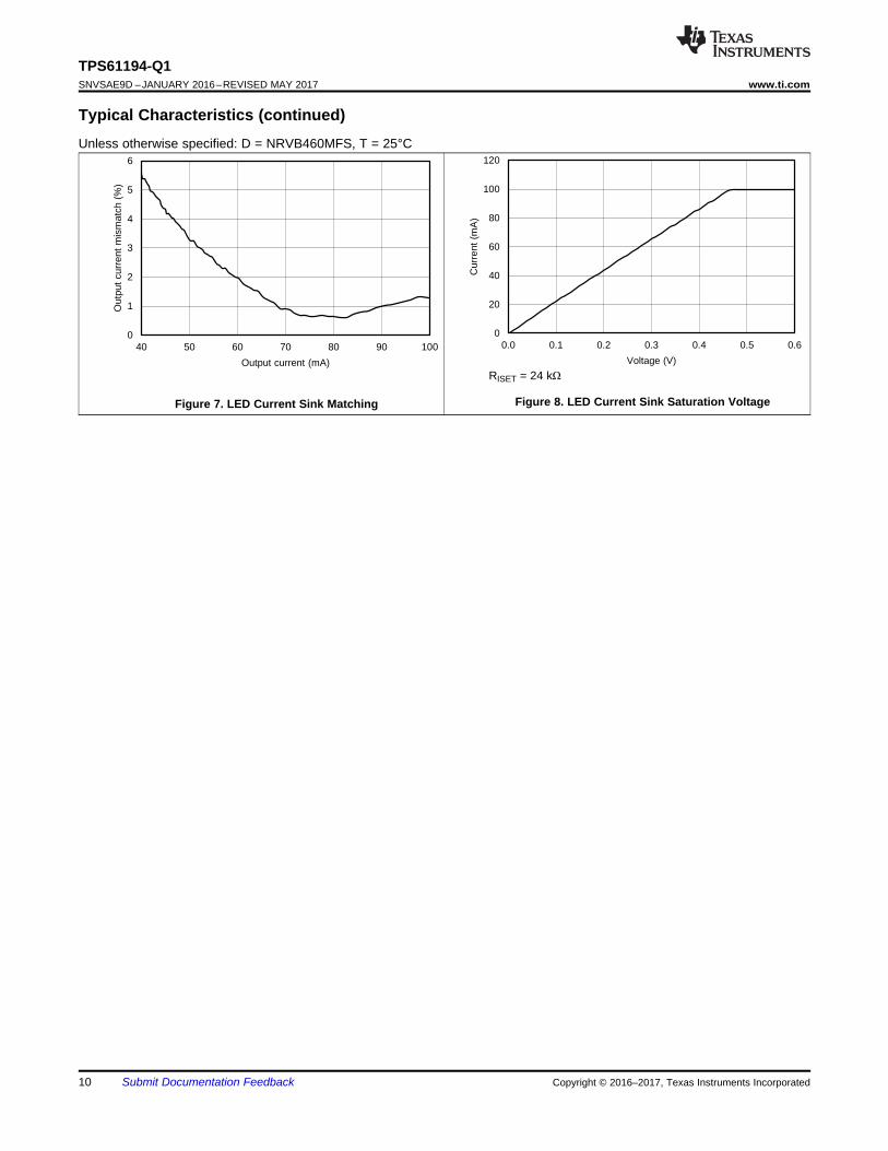
Figure 7. LED Current Sink Matching
RISET = 24 kΩ
Figure 8. LED Current Sink Saturation Voltage
11
TPS61194-Q1www.ti.com SNVSAE9D –JANUARY 2016–REVISED MAY 2017
Submit Documentation FeedbackCopyright © 2016–2017, Texas Instruments Incorporated
8 Detailed Description
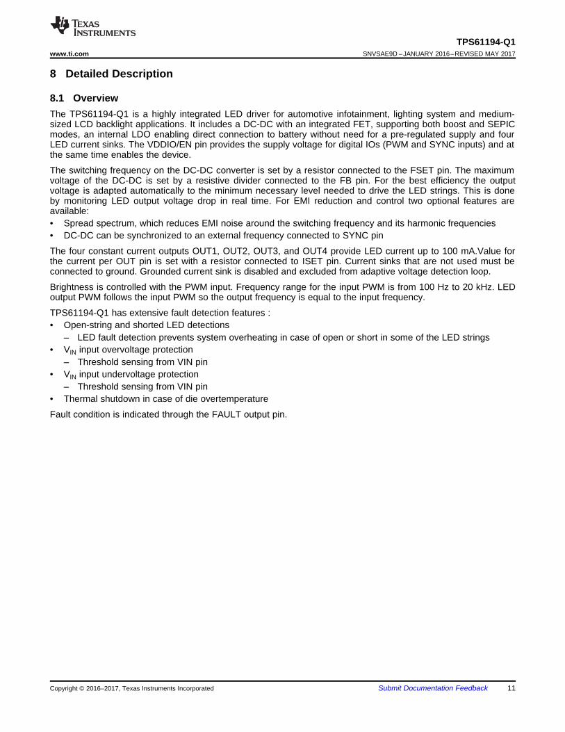
8.1 OverviewThe TPS61194-Q1 is a highly integrated LED driver for automotive infotainment, lighting system and medium-sized LCD backlight applications. It includes a DC-DC with an integrated FET, supporting both boost and SEPICmodes, an internal LDO enabling direct connection to battery without need for a pre-regulated supply and fourLED current sinks. The VDDIO/EN pin provides the supply voltage for digital IOs (PWM and SYNC inputs) and atthe same time enables the device.
The switching frequency on the DC-DC converter is set by a resistor connected to the FSET pin. The maximumvoltage of the DC-DC is set by a resistive divider connected to the FB pin. For the best efficiency the outputvoltage is adapted automatically to the minimum necessary level needed to drive the LED strings. This is doneby monitoring LED output voltage drop in real time. For EMI reduction and control two optional features areavailable:• Spread spectrum, which reduces EMI noise around the switching frequency and its harmonic frequencies• DC-DC can be synchronized to an external frequency connected to SYNC pin
The four constant current outputs OUT1, OUT2, OUT3, and OUT4 provide LED current up to 100 mA.Value forthe current per OUT pin is set with a resistor connected to ISET pin. Current sinks that are not used must beconnected to ground. Grounded current sink is disabled and excluded from adaptive voltage detection loop.
Brightness is controlled with the PWM input. Frequency range for the input PWM is from 100 Hz to 20 kHz. LEDoutput PWM follows the input PWM so the output frequency is equal to the input frequency.
TPS61194-Q1 has extensive fault detection features :• Open-string and shorted LED detections
– LED fault detection prevents system overheating in case of open or short in some of the LED strings• VIN input overvoltage protection
– Threshold sensing from VIN pin• VIN input undervoltage protection
– Threshold sensing from VIN pin• Thermal shutdown in case of die overtemperature
Fault condition is indicated through the FAULT output pin.

COUT
D
VIN
LDO
CLDOSW
FB
BOOST CONTROLLER
VIN
SYNC
PGND
OUT1
OUT2
GND
LED CURRENT
SINKS
ANALOG BLOCKS(CLOCK GENERATOR,
VREF, TSD etc.)
DIGITAL BLOCKS(FSM, ADAPTIVE VOLTAGE CONTROL, SAFETY LOGIC
etc.)
VDDIO/EN
FAULT
RISET
EXPOSED PAD
LDO
ISET
CURRENT SETTING
FSETRFSET
PWM
VDDIO
CIN
L
OUT3
OUT4
VOUT
R1
R2
12
TPS61194-Q1SNVSAE9D –JANUARY 2016–REVISED MAY 2017 www.ti.com
Submit Documentation Feedback Copyright © 2016–2017, Texas Instruments Incorporated
8.2 Functional Block Diagram

10
15
20
25
30
35
40
45
200 300 400 500 600 700 800 900 1000
Max
imum
Con
vert
er O
utpu
t V
olta
ge (
V)
R1 (k )
C008
BGBOOST BG
VV K 0.0387 R1 V
R2·§
u u ¨ ¸© ¹
13
TPS61194-Q1www.ti.com SNVSAE9D –JANUARY 2016–REVISED MAY 2017
Submit Documentation FeedbackCopyright © 2016–2017, Texas Instruments Incorporated
8.3 Feature Description
8.3.1 Integrated DC-DC ConverterThe TPS61194-Q1 DC-DC converter generates supply voltage for the LEDs and can operate in boost mode or inSEPIC mode. The maximum output voltage VOUT_MAX is defined by an external resistive divider (R1, R2).
VOUT_MAX voltage should be chosen based on the maximum voltage required for LED strings. Recommendedmaximum voltage is about 30% higher than maximum LED string voltage. DC-DC output voltage is adjustedautomatically based on LED current sink headroom voltage. Maximum, minimum, and initial boost voltages canbe calculated with Equation 1:
where• VBG = 1.2 V• R2 recommended value is 130 kΩ• Resistor values are in kΩ• K = 1 for maximum adaptive boost voltage (typical)• K = 0 for minimum adaptive boost voltage (typical)• K = 0.88 for initial boost voltage (typical) (1)
Figure 9. Maximum Converter Output Voltage vs R1 Resistance
Alternatively, a T-divider can be used if resistance less than 100 kΩ is required for the external resistive divider.Refer to Using the TPS61194-Q1 Evaluation Module for details.
The converter is a current mode DC-DC converter, where the inductor current is measured and controlled withthe feedback. Switching frequency is adjustable between 250 kHz and 2.2 MHz with RFSET resistor asEquation 2:
ƒSW = 67600 / (RFSET + 6.4)
where• ƒSW is switching frequency, kHz• RFSET is frequency setting resistor, kΩ (2)
In most cases lower frequency has higher system efficiency. DC-DC internal parameters are chosenautomatically according to the selected switching frequency (see Table 2) to ensure stability. In boost mode a 15-pF capacitor CFB must be placed across resistor R1 when operating in 300-kHz to 500-kHz range (see TypicalApplication for 4 LED Strings). When operating in the 1.8-MHz to 2.2-MHz range CFB = 4.7 pF.
RC filter
BOOST OSCILLATOR
SYNC
FB
OFF/BLANK TIME
PULSE GENERATOR
CURRENT RAMP
GENERATOR
BLANK TIME
SW
OVP
S
OCP
LIGHTLOAD
R
RRR-
+
FSET FSET CTRL
GM
GM
RFSET
ADAPTIVE VOLTAGE CONTROL
CIN
D
COUT
VIN
CURRENT SENSE
PGND
VOUT
R1
R2
14
TPS61194-Q1SNVSAE9D –JANUARY 2016–REVISED MAY 2017 www.ti.com
Submit Documentation Feedback Copyright © 2016–2017, Texas Instruments Incorporated
Feature Description (continued)
Figure 10. Boost Block Diagram
DC-DC can be driven by an external SYNC signal between 300 kHz and 2.2 MHz. If the external synchronizationinput disappears, DC-DC continues operation at the frequency defined by RFSET resistor. When externalfrequency disappears and SYNC pin level is low, converter continues operation without spread spectrumimmediately. If SYNC remains high, converter continues switching with spread spectrum enabled after 256 µs.
External SYNC frequency must be 1.2 to 1.5 times higher than the frequency defined by RFSET resistor. Minimumfrequency setting with RFSET is 250 kHz to support 300-kHz switching with external clock.
The optional spread spectrum feature (±3% from central frequency, 1-kHz modulation frequency) reduces EMInoise at the switching frequency and its harmonic frequencies. When external synchronization is used, spreadspectrum is not available.
Table 1. DC-DC Synchronization ModeSYNC PIN INPUT MODE
Low Spread spectrum disabledHigh Spread spectrum enabled
300 to 2200 kHz frequency Spread spectrum disabled, external synchronization mode
(1) Parameters are for reference only(2) Due to current sensing comparator delay the actual minimum off time is 6 ns (typical) longer than in the table.
Table 2. DC-DC Parameters (1)
RANGE FREQUENCY(kHz)
TYPICALINDUCTANCE (µH)
TYPICAL BOOST INPUTAND OUTPUT
CAPACITORS (µF)
MINIMUM SWITCHOFF TIME (ns)(2)
BLANKTIME (ns)
CURRENTRAMP (A/s)
CURRENT RAMPDELAY (ns)
1 300 to 480 33 2 ×10 (cer.) + 33 (electr.) 150 95 24 550
2 480 to 1150 15 10 (cer.) + 33 (electr.) 60 95 43 300
3 1150 to 1650 10 3 × 10 (cer.) 40 95 79 0
4 1650 to 2200 4.7 3 × 10 (cer.) 40 70 145 0
RISET = 2342 / (IOUT ± 2.5)
15
TPS61194-Q1www.ti.com SNVSAE9D –JANUARY 2016–REVISED MAY 2017
Submit Documentation FeedbackCopyright © 2016–2017, Texas Instruments Incorporated
The converter SW pin DC current is limited to 2 A (typical). To support warm-start transient condition the currentlimit is automatically increased to 2.5 A for a short period of 1.5 seconds when a 2-A limit is reached.
NOTEApplication condition where the 2-A limit is exceeded continuously is not allowed. In thiscase the current limit would be 2 A for 1.5 seconds followed by 2.5-A limit for 1.5 seconds,and this 3-second period repeats.
To keep switching voltage within safe levels there is a 48-V limit comparator in the event that FB loop is broken.
8.3.2 Internal LDOThe internal LDO regulator converts the input voltage at VIN to a 4.3-V output voltage for internal use. Connect aminimum of 1-µF ceramic capacitor from LDO pin to ground, as close to the LDO pin as possible.
8.3.3 LED Current Sinks
8.3.3.1 Output ConfigurationTPS61194-Q1 detects LED output configuration during start-up. Any current sink output connected to ground isdisabled and excluded from the adaptive voltage control of the DC-DC and fault detections.
8.3.3.2 Current SettingMaximum current for the LED outputs is controlled with external RISET resistor. RISET value for target maximumcurrent can be calculated using Equation 3:
where• RISET is current setting resistor, kΩ• ILED is output current per output, mA (3)
8.3.3.3 Brightness ControlTPS61194-Q1 controls the brightness of the display with conventional PWM. Output PWM directly follows theinput PWM. Input PWM frequency can be in the range of 100 Hz to 20 kHz.
8.3.4 Protection and Fault DetectionsThe TPS61194-Q1 has fault detection for LED open and short, VIN input overvoltage protection (VIN_OVP) , VINundervoltage lockout (VIN_UVLO), and thermal shutdown (TSD).
8.3.4.1 Adaptive DC-DC Voltage Control and Functionality of LED Fault ComparatorsAdaptive voltage control function adjusts the DC-DC output voltage to the minimum sufficient voltage for properLED current sink operation. The current sink with highest VF LED string is detected and DC-DC output voltageadjusted accordingly. DC-DC adaptive control voltage step size is defined by maximum voltage setting, VSTEP =(VOUT_MAX – VOUT_MIN) / 256. Periodic down pressure is applied to the target voltage to achieve better systemefficiency.
Every LED current sink has 3 comparators for the adaptive DC-DC control and LED fault detections. Comparatoroutputs are filtered, filtering time is 1 µs.
OU
T1
OU
T2
OU
T3
OU
T4
OU
T1
OU
T2
OU
T3
OU
T4
OU
T1
OU
T2
OU
T3
OU
T4
Minimum headroom
level reached
OU
T1
OU
T2
OU
T3
OU
T4
Open LED fault
OU
T1
OU
T2
OU
T3
OU
T4
Shorted LED fault
LOW_COMP
MID_COMP
HIGH_COMP
VO
UT V
OLT
AG
E
No actions No actionsDCDC
increasesvoltage
Open LED fault when VOUT = VOUT_MAX
Shorted LED fault (at least one output should
be between LOW_COMP and MID_COMP)
OU
T1
OU
T2
OU
T3
OU
T4
All outputs are above headroom
window
DCDC decreases
voltage
HEADROOMWINDOW
HIGH_COMP
MID_COMP
LOW_COMP
OUT#
CURRENT/PWM
CONTROL
LOWEST VOLTAGE
SHORT STRING
DETECTION LEVEL
VOLTAGE THRESHOLD
16
TPS61194-Q1SNVSAE9D –JANUARY 2016–REVISED MAY 2017 www.ti.com
Submit Documentation Feedback Copyright © 2016–2017, Texas Instruments Incorporated
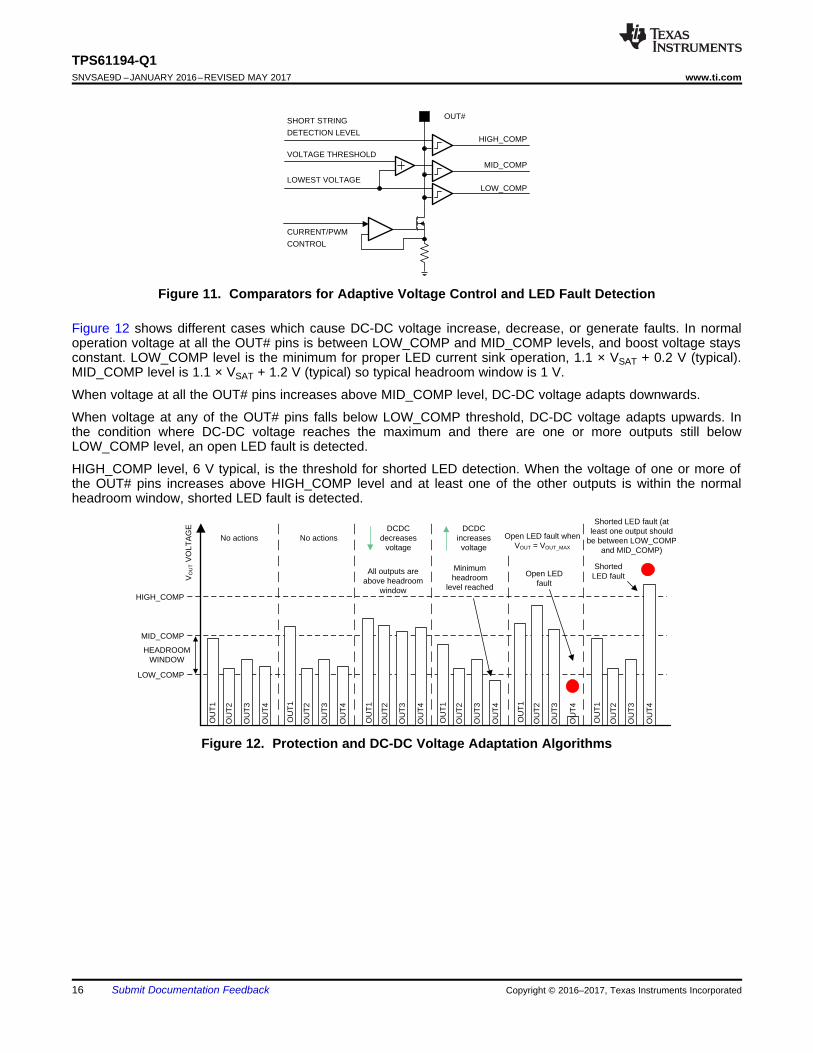
Figure 11. Comparators for Adaptive Voltage Control and LED Fault Detection
Figure 12 shows different cases which cause DC-DC voltage increase, decrease, or generate faults. In normaloperation voltage at all the OUT# pins is between LOW_COMP and MID_COMP levels, and boost voltage staysconstant. LOW_COMP level is the minimum for proper LED current sink operation, 1.1 × VSAT + 0.2 V (typical).MID_COMP level is 1.1 × VSAT + 1.2 V (typical) so typical headroom window is 1 V.
When voltage at all the OUT# pins increases above MID_COMP level, DC-DC voltage adapts downwards.
When voltage at any of the OUT# pins falls below LOW_COMP threshold, DC-DC voltage adapts upwards. Inthe condition where DC-DC voltage reaches the maximum and there are one or more outputs still belowLOW_COMP level, an open LED fault is detected.
HIGH_COMP level, 6 V typical, is the threshold for shorted LED detection. When the voltage of one or more ofthe OUT# pins increases above HIGH_COMP level and at least one of the other outputs is within the normalheadroom window, shorted LED fault is detected.
Figure 12. Protection and DC-DC Voltage Adaptation Algorithms

17
TPS61194-Q1www.ti.com SNVSAE9D –JANUARY 2016–REVISED MAY 2017
Submit Documentation FeedbackCopyright © 2016–2017, Texas Instruments Incorporated
8.3.4.2 Overview of the Fault/Protection SchemesA summary of the TPS61194-Q1fault detection behavior is shown in Table 3. Detected faults (excluding LEDopen or short) cause device to enter FAULT_RECOVERY state. In FAULT_RECOVERY the DC-DC and LEDcurrent sinks of the device are disabled, and the FAULT pin is pulled low. The device recovers automatically andenters normal operating mode (ACTIVE) after a recovery time of 100 ms if the fault condition has disappeared.When recovery is succesful, FAULT pin is released.
If a LED fault is detected, the device continues normal operation and only the faulty string is disabled. The fault isindicated via the FAULT pin which can be released by toggling VDDIO/EN pin low for a short period of 2 µs to 20µs. LEDs are turned off for this period but the device stays in ACTIVE mode. If VDDIO/EN is low longer, thedevice goes to STANDBY and restarts when EN goes high again.
Table 3. Fault Detections
FAULT/PROTECTION FAULT NAME THRESHOLD FAULT
PINFAULT_
RECOVERYSTATE
ACTION
VINovervoltageprotection
VIN_OVP
1. VIN > 42 V2. VOUT >VSET_DCDC + 6..10V.VSET_DCDC isvoltage valuedefined by logicduring adaptation
Yes Yes
1. Overvoltage is monitored from the beginning of softstart. Fault is detected if the duration of overvoltagecondition is 100 µs minimum.2. Overvoltage is monitored from the beginning ofnormal operation (ACTIVE mode). Fault is detected ifover-voltage condition duration is 560 ms minimum(tfilter). After the first fault, detection filter time is reducedto 50 ms for following recovery cycles. When the devicerecovers and has been in ACTIVE mode for 160 ms,filter time is increased back to 560 ms .
VINundervoltagelockout
VIN_UVLO Falling 3.9 VRising 4 V Yes Yes
Detects undervoltage condition at VIN pin. Sensed in alloperating modes. Fault is detected if undervoltagecondition duration is 100 µs minimum.
Open LED fault OPEN_LED LOW_COMPthreshold Yes No
Detected if the voltage of one or more current sinks isbelow threshold level, and DC-DC adaptive control hasreached maximum voltage. Open string is removed fromthe DC-DC voltage control loop and current sink isdisabled.Fault pin is released by toggling VDDIO/EN pin. IfVDDIO/EN is low for a period of 2 µs to 20 µs, LEDs areturned off for this period but device stays ACTIVE. IfVDDIO/EN is low longer, device goes to STANDBY andrestarts when EN goes high again.
Shorted LEDfault SHORT_LED Shorted string
detection level 6 V Yes No
Detected if the voltage of one or more current sinks isabove shorted string detection level and at least oneOUTx voltage is within headroom window. Shorted stringis removed from the DC-DC voltage control loop andcurrent sink is disabled.Fault pin is released by toggling VDDIO/EN pin. IfVDDIO/EN is low for a period of 2…20 µs, LEDs areturned off for this period but device stays ACTIVE. IfVDDIO/EN is low longer, device goes to STANDBY andrestarts when EN goes high again..
Thermalprotection TSD
165ºCThermal shutdown
hysteresis 20ºCYes Yes
Thermal shutdown is monitored from the beginning ofsoft start. Die temperature must decrease by 20ºC fordevice to recover.

VIN
FB
UVLO rising threshold
FAULT
UVLO falling threshold
ttRECOVERY = 100 mst ttRECOVERY = 100 mstttSOFTSTART +tttBOOST STARTUPt
VIN
FB
VIN OVP threshold
ttRECOVERY = 100 mst
DCDC OVP threshold
FAULT ttRECOVERY = 100 mstttSOFTSTART +tttBOOST STARTUPt
VIN
tRECOVERY = 100 ms
FAULT
tFILTER = 560 ms
VOUT
tSOFTSTART + tBOOST START
tFILTER = 50 ms
tRECOVERY = 100 ms
tSOFTSTART + tBOOST START
tFILTER = 40 - 50 ms
tSOFTSTART + tBOOST START
tFILTER = 50 ms
tRECOVERY = 100 ms
VIN OVERVOLTAGEVIN OK
IOUT
Time is not enough to discharge COUT
VSET_DCDC + 6...10 V
18
TPS61194-Q1SNVSAE9D –JANUARY 2016–REVISED MAY 2017 www.ti.com
Submit Documentation Feedback Copyright © 2016–2017, Texas Instruments Incorporated
Figure 13. VIN Overvoltage Protection (DC-DC OVP)
Figure 14. VIN Overvoltage Protection (VIN OVP)
Figure 15. VIN Undervoltage Lockout

VDDIO/EN
OUT# pin Other LEDs
FAULT
t = 2...20 µs
OUTT# pin Shorted LED HIGH_COMP level
LOW_COMP level
MID_COMP level
VOUT
VDDIO/EN
OUT# pin Other LEDs
FAULT
t = 2...20 µs
OUT# pin Open LED
LOW_COMP level
VOUT_MAX
19
TPS61194-Q1www.ti.com SNVSAE9D –JANUARY 2016–REVISED MAY 2017
Submit Documentation FeedbackCopyright © 2016–2017, Texas Instruments Incorporated
Figure 16. LED Open Fault
Figure 17. LED Short Fault
8.4 Device Functional Modes
8.4.1 Device StatesThe TPS61194-Q1 enters STANDBY mode when the internal LDO output rises above the power-on reset level,VLDO > VPOR. In STANDBY mode the device is able to detect VDDIO/EN signal. When VDDIO/EN is pulled high,the device powers up. After start LED outputs are sensed to detect grounded outputs. Grounded outputs aredisabled and excluded from the adaptive voltage control loop of the DC-DC.
If a fault condition is detected, the device enters FAULT_RECOVERY state. Faults that cause the device to enterFAULT_RECOVERY are listed in Table 3. When LED open or short is detected, the faulty string is disabled, butdevice stays in ACTIVE mode.

VIN
LDO
VOUT
PWM OUT
IQ
Headroom adaptation
Active mode
VDDIO/EN
VOUT=VIN level ± diode drop
SOFTSTART
BOOSTSTART
t>500s
SYNC
T=50s
STANDBYPOR=1
VDDIO/EN=1
BOOST START
SOFT START
ACTIVE
65 ms
50 ms
SHUTDOWN
FAULT RECOVERY
FAULTS:- VIN_OVP- VIN_UVLO- TSD
100 ms
FAULTS
FAULTS
VDDIO/EN=0
VDDIO/EN=0
LED OUTPUT CONFIGURATION
DETECTION
DC-DC AND LED CURRENT SINKS ARE DISABLED IN FAULT RECOVERY STATE
FAULT RECOVERY?
YES
NO
VIN_OVPVIN_UVLOTSD
20
TPS61194-Q1SNVSAE9D –JANUARY 2016–REVISED MAY 2017 www.ti.com
Submit Documentation Feedback Copyright © 2016–2017, Texas Instruments Incorporated
Device Functional Modes (continued)
Figure 18. State Diagram
Figure 19. Timing Diagram for the Typical Start-Up and Shutdown
TPS61194-Q1
FB
PWM
OUT1
OUT2
L1 D1 Up to 37 V5...28 V
COUT
RISET
Up to 100 mA/string
SW
LDO
FSET
VIN
VDDIO/EN
PGND GND PAD
VIN
ISETFAULT
VDDIO
FAULT
RFSET
R1R2
R3
CLDO
BRIGHTNESS
SYNC
EN
CIN
CIN BOOST
OUT3
CFB
OUT4
21
TPS61194-Q1www.ti.com SNVSAE9D –JANUARY 2016–REVISED MAY 2017
Submit Documentation FeedbackCopyright © 2016–2017, Texas Instruments Incorporated
9 Application and Implementation
NOTEInformation in the following applications sections is not part of the TI componentspecification, and TI does not warrant its accuracy or completeness. TI’s customers areresponsible for determining suitability of components for their purposes. Customers shouldvalidate and test their design implementation to confirm system functionality.
9.1 Application InformationThe TPS61194-Q1 is designed for automotive applications, and an input voltage (VIN), intended to be connectedto the automotive battery, supports input voltage range from 4.5 V to 40 V. Device internal circuitry is poweredfrom the integrated LDO.
The TPS61194-Q1 uses a simple four-wire control:• VDDIO/EN for enable• PWM input for brightness control• SYNC pin for boost synchronisation (optional)• FAULT output to indicate fault condition (optional)
9.2 Typical Applications
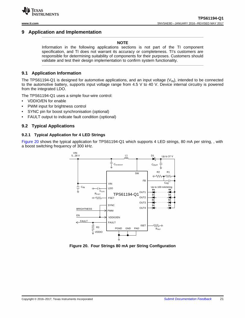
9.2.1 Typical Application for 4 LED StringsFigure 20 shows the typical application for TPS61194-Q1 which supports 4 LED strings, 80 mA per string, , witha boost switching frequency of 300 kHz.
Figure 20. Four Strings 80 mA per String Configuration
ISAT >
x(VOUT - VIN)
VOUT
VIN
Where D =
Where IRIPPLE = (2 x L x f)
DQG'¶= (1 - D)(VOUT ± VIN)
(VOUT)
+ IRIPPLEIOUTMAX '¶
For Boost
22
TPS61194-Q1SNVSAE9D –JANUARY 2016–REVISED MAY 2017 www.ti.com
Submit Documentation Feedback Copyright © 2016–2017, Texas Instruments Incorporated
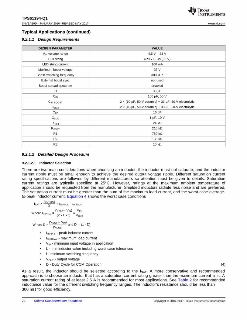
Typical Applications (continued)9.2.1.1 Design Requirements
DESIGN PARAMETER VALUEVIN voltage range 4.5 V – 28 V
LED string 4P8S LEDs (30 V)LED string current 100 mA
Maximum boost voltage 37 VBoost switching frequency 300 kHz
External boost sync not usedBoost spread spectrum enabled
L1 33 μHCIN 100 µF, 50 V
CIN BOOST 2 × (10-µF, 50-V ceramic) + 33-µF, 50-V electrolyticCOUT 2 × (10-µF, 50-V ceramic) + 33-µF, 50-V electrolyticCFB 15 pF
CLDO 1 µF, 10 VRISET 24 kΩRFSET 210 kΩ
R1 750 kΩR2 130 kΩR3 10 kΩ
9.2.1.2 Detailed Design Procedure
9.2.1.2.1 Inductor Selection
There are two main considerations when choosing an inductor; the inductor must not saturate, and the inductorcurrent ripple must be small enough to achieve the desired output voltage ripple. Different saturation currentrating specifications are followed by different manufacturers so attention must be given to details. Saturationcurrent ratings are typically specified at 25°C. However, ratings at the maximum ambient temperature ofapplication should be requested from the manufacturer. Shielded inductors radiate less noise and are preferred.The saturation current must be greater than the sum of the maximum load current, and the worst case average-to-peak inductor current. Equation 4 shows the worst case conditions
• IRIPPLE - peak inductor current• IOUTMAX - maximum load current• VIN - minimum input voltage in application• L - min inductor value including worst case tolerances• f - minimum switching frequency• VOUT - output voltage• D - Duty Cycle for CCM Operation (4)
As a result, the inductor should be selected according to the ISAT. A more conservative and recommendedapproach is to choose an inductor that has a saturation current rating greater than the maximum current limit. Asaturation current rating of at least 2.5 A is recommended for most applications. See Table 2 for recommendedinductance value for the different switching frequency ranges. The inductor’s resistance should be less than300 mΩ for good efficiency.
65
70
75
80
85
90
95
100
0 20 40 60 80 100
Boo
st e
ffici
ency
(%
)
Brightness (%)
VIN=5V
VIN=8V
VIN=12V
VIN=16V
C011
65
70
75
80
85
90
95
100
0 20 40 60 80 100
Sys
tem
effi
cien
cy (
%)
Brightness (%)
VIN=5V
VIN=8V
VIN=12V
VIN=16V
C012
23
TPS61194-Q1www.ti.com SNVSAE9D –JANUARY 2016–REVISED MAY 2017
Submit Documentation FeedbackCopyright © 2016–2017, Texas Instruments Incorporated
See detailed information in Understanding Boost Power Stages in Switch Mode Power Supplies. Power StageDesigner™ Tool can be used for the boost calculation: http://www.ti.com/tool/powerstage-designer.
9.2.1.2.2 Output Capacitor Selection
A ceramic capacitor with 2 × VMAX BOOST or more voltage rating is recommended for the output capacitor. TheDC-bias effect can reduce the effective capacitance by up to 80%, which needs to be considered in capacitancevalue selection. Capacitance recommendations for different switching frequencies are shown in Table 2. Tominimize audible noise of ceramic capacitors their physical size should typically be minimized.
9.2.1.2.3 Input Capacitor Selection
A ceramic capacitor with 2 × VIN MAX or more voltage rating is recommended for the input capacitor. The DC-biaseffect can reduce the effective capacitance by up to 80%, which needs to be considered in capacitance valueselection. Capacitance recommendations for different boost switching frequencies are shown in Table 2.
9.2.1.2.4 LDO Output Capacitor
A ceramic capacitor with at least 10-V voltage rating is recommended for the output capacitor of the LDO. TheDC-bias effect can reduce the effective capacitance by up to 80%, which needs to be considered in capacitancevalue selection. Typically a 1-µF capacitor is sufficient.
9.2.1.2.5 Diode
A Schottky diode should be used for the boost output diode. Do not use ordinary rectifier diodes because slowswitching speeds and long recovery times degrade the efficiency and the load regulation. Diode rating for peakrepetitive current should be greater than inductor peak current (up to 3 A) to ensure reliable operation in boostmode. Average current rating should be greater than the maximum output current. Schottky diodes with a lowforward drop and fast switching speeds are ideal for increasing efficiency. Choose a reverse breakdown voltageof the Schottky diode significantly larger than the output voltage.
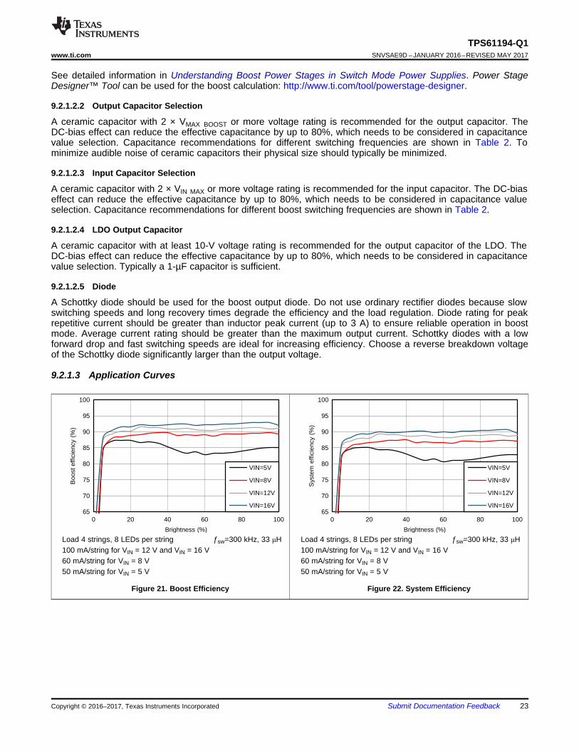
9.2.1.3 Application Curves
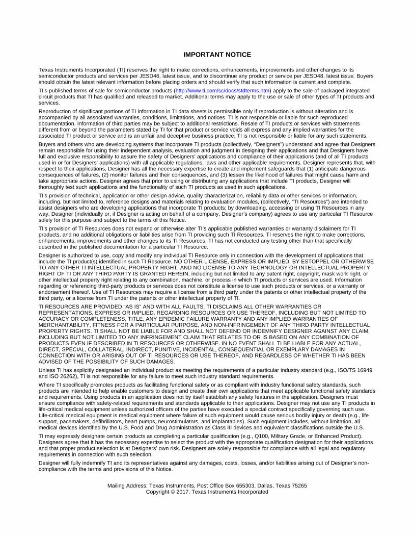
Load 4 strings, 8 LEDs per string ƒsw=300 kHz, 33 μH100 mA/string for VIN = 12 V and VIN = 16 V60 mA/string for VIN = 8 V50 mA/string for VIN = 5 V
Figure 21. Boost Efficiency
Load 4 strings, 8 LEDs per string ƒsw=300 kHz, 33 μH100 mA/string for VIN = 12 V and VIN = 16 V60 mA/string for VIN = 8 V50 mA/string for VIN = 5 V
Figure 22. System Efficiency

TPS61194-Q1
FB
PWM
OUT1
L1
D1
COUT
RISET
Up to 100 mA/string
SW
LDO
FSET
VIN
VDDIO/EN
PGND GND PAD
VIN
ISETFAULT
VDDIO
FAULT
EN
RFSET
R1R2
R3
BRIGHTNESS
BOOST SYNCSYNC
C1
CLDO
CIN SEPIC
CIN
OUT3
OUT2
OUT4
20ms/div OUT1/OUT2/BOOST 10V/div FAULT 2V/div
24
TPS61194-Q1SNVSAE9D –JANUARY 2016–REVISED MAY 2017 www.ti.com
Submit Documentation Feedback Copyright © 2016–2017, Texas Instruments Incorporated
Figure 23. Typical Start-Up Figure 24. Open LED Fault
9.2.2 SEPIC Mode ApplicationWhen LED string voltage can be above or below VIN voltage, SEPIC configuration can be used. In this example,two separate coils are used for SEPIC. This can enable lower height external components to be used, comparedto a coupled coil solution. On the other hand, coupled coil typically maximizes the efficiency. Also, in thisexample, an external clock is used to synchronize SEPIC switching frequency. External clock input can bemodulated to spread switching frequency spectrum.
Figure 25. SEPIC Mode, 4 Strings, 100 mA per String Configuration
25
TPS61194-Q1www.ti.com SNVSAE9D –JANUARY 2016–REVISED MAY 2017
Submit Documentation FeedbackCopyright © 2016–2017, Texas Instruments Incorporated
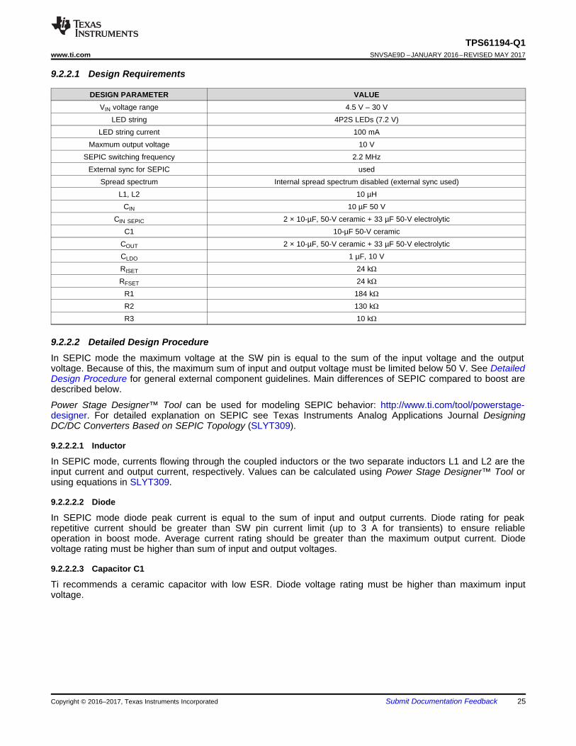
9.2.2.1 Design Requirements
DESIGN PARAMETER VALUEVIN voltage range 4.5 V – 30 V
LED string 4P2S LEDs (7.2 V)LED string current 100 mA
Maxmum output voltage 10 VSEPIC switching frequency 2.2 MHz
External sync for SEPIC usedSpread spectrum Internal spread spectrum disabled (external sync used)
L1, L2 10 µHCIN 10 µF 50 V
CIN SEPIC 2 × 10-µF, 50-V ceramic + 33 µF 50-V electrolyticC1 10-µF 50-V ceramic
COUT 2 × 10-µF, 50-V ceramic + 33 µF 50-V electrolyticCLDO 1 µF, 10 VRISET 24 kΩRFSET 24 kΩ
R1 184 kΩR2 130 kΩR3 10 kΩ
9.2.2.2 Detailed Design ProcedureIn SEPIC mode the maximum voltage at the SW pin is equal to the sum of the input voltage and the outputvoltage. Because of this, the maximum sum of input and output voltage must be limited below 50 V. See DetailedDesign Procedure for general external component guidelines. Main differences of SEPIC compared to boost aredescribed below.
Power Stage Designer™ Tool can be used for modeling SEPIC behavior: http://www.ti.com/tool/powerstage-designer. For detailed explanation on SEPIC see Texas Instruments Analog Applications Journal DesigningDC/DC Converters Based on SEPIC Topology (SLYT309).
9.2.2.2.1 Inductor
In SEPIC mode, currents flowing through the coupled inductors or the two separate inductors L1 and L2 are theinput current and output current, respectively. Values can be calculated using Power Stage Designer™ Tool orusing equations in SLYT309.
9.2.2.2.2 Diode
In SEPIC mode diode peak current is equal to the sum of input and output currents. Diode rating for peakrepetitive current should be greater than SW pin current limit (up to 3 A for transients) to ensure reliableoperation in boost mode. Average current rating should be greater than the maximum output current. Diodevoltage rating must be higher than sum of input and output voltages.
9.2.2.2.3 Capacitor C1
Ti recommends a ceramic capacitor with low ESR. Diode voltage rating must be higher than maximum inputvoltage.

Brightness (%)
SE
PIC
Sys
tem
Effi
cien
cy (
%)
0 10 20 30 40 50 60 70 80 90 1003035404550556065707580859095
100
D001
VIN = 5VVIN = 8VVIN = 12VVIN = 15V
Brightness (%)
SE
PIC
Effi
cien
cy (
%)
0 10 20 30 40 50 60 70 80 90 10050
55
60
65
70
75
80
85
90
95
100
D001
VIN=5VVIN=5VVIN=12VVIN=15V
Brightness (%)
SE
PIC
Effi
cien
cy (
%)
0 10 20 30 40 50 60 70 80 90 1003035404550556065707580859095
100
D001
VIN = 5VVIN = 8VVIN = 12VVIN = 15V
26
TPS61194-Q1SNVSAE9D –JANUARY 2016–REVISED MAY 2017 www.ti.com
Submit Documentation Feedback Copyright © 2016–2017, Texas Instruments Incorporated
9.2.2.3 Application Curves
Load 100mA per string, 3 strings, 2 LEDs per stringƒsw = 2.2 MHz2 × 10 μH, IHLP2525BDER100M
Figure 26. SEPIC Efficiency
Load 100mA per string, 4 strings, 2 LEDs per stringfsw = 2.2 MHz2 × 10 μH, IHLP2525BDER100M
Figure 27. SEPIC Efficiency
Load 100mA/string, 4 strings, 2 LEDs per stringfsw = 2.2 MHz2 x 10 μH, IHLP2525BDER100M
Figure 28. System Efficiency
10 Power Supply RecommendationsThe device is designed to operate from an automotive battery. Device should be protected from reversal voltageand voltage dump over 50 V. The resistance of the input supply rail must be low enough so that the input currenttransient does not cause too high drop at TPS61194-Q1 VIN pin. If the input supply is connected by using longwires additional bulk capacitance may be required in addition to the ceramic bypass capacitors in the VIN line.
27
TPS61194-Q1www.ti.com SNVSAE9D –JANUARY 2016–REVISED MAY 2017
Submit Documentation FeedbackCopyright © 2016–2017, Texas Instruments Incorporated
11 Layout
11.1 Layout GuidelinesFigure 29 is a layout recommendation for TPS61194-Q1 used to demonstrate the principles of a good layout.This layout can be adapted to the actual application layout if or where possible. It is important that all boostcomponents are close to the chip, and the high current traces must be wide enough. By placing boostcomponents on one side of the chip it is easy to keep the ground plane intact below the high current paths. Thisway other chip pins can be routed more easily without splitting the ground plane. Bypass LDO capacitor must beplaced as close as possible to the device.
Here are some main points to help the PCB layout work:• Current loops need to be minimized:
– For low frequency the minimal current loop can be achieved by placing the boost components as close aspossible to the SW and PGND pins. Input and output capacitor grounds must be close to each other tominimize current loop size.
– Minimal current loops for high frequencies can be achieved by making sure that the ground plane is intactunder the current traces. High-frequency return currents find a route with minimum impedance, which isthe route with minimum loop area, not necessarily the shortest path. Minimum loop area is formed whenreturn current flows just under the positivecurrent route in the ground plane, if the ground plane is intactunder the route.
• The GND plane must be intact under the high current boost traces to provide shortest possible return pathand smallest possible current loops for high frequencies.
• Current loops when the boost switch is conducting and not conducting must be on the same direction inoptimal case.
• Inductors must be placed so that the current flows in the same direction as in the current loops. Rotatinginductor 180° changes current direction.
• Use separate power and noise-free grounds. Power ground is used for boost converter return current andnoise-free ground for more sensitive signals, such as LDO bypass capacitor grounding as well as groundingthe GND pin of the device.
• Boost output feedback voltage to LEDs must be taken out after the output capacitors, not straight from thediode cathode.
• Place LDO 1-µF bypass capacitor as close as possible to the LDO pin.• Input and output capacitors require strong grounding (wide traces, many vias to GND plane).• If two output capacitors are used they must have symmetrical layout to get both capacitors working ideally.• Output ceramic capacitors have a DC-bias effect. If the output capacitance is too low, it can cause boost to
become unstable on some loads, and this increases EMI. DC-bias characteristics should be obtained fromthe component manufacturer; they are not taken into account on component tolerance. TI recommendsX5R/X7R capacitors.

1
2
3
4
5
6
7
8
9
10
20
19
18
17
16
15
14
13
12
11
OUT2
GND
OUT3
OUT4
NC
LDO
VDDIO/EN
FSET
VIN VIN
NC
FB
SW
OUT1
GND
PWM
FAULT
ISET
SYNC
VIN
LED
ST
RIN
GS
LDO
RISET
RFSET
VBOOST
PGND
28
TPS61194-Q1SNVSAE9D –JANUARY 2016–REVISED MAY 2017 www.ti.com
Submit Documentation Feedback Copyright © 2016–2017, Texas Instruments Incorporated
11.2 Layout Example
Figure 29. TPS61194-Q1 Boost Layout

29
TPS61194-Q1www.ti.com SNVSAE9D –JANUARY 2016–REVISED MAY 2017
Submit Documentation FeedbackCopyright © 2016–2017, Texas Instruments Incorporated
12 Device and Documentation Support
12.1 Device Support
12.1.1 Development SupportPower Stage Designer™ Tool can be used for both boost and SEPIC: http://www.ti.com/tool/powerstage-designer
12.2 Documentation Support
12.2.1 Related DocumentationFor related documentation see the following:• PowerPAD™ Thermally Enhanced Package• Understanding Boost Power Stages in Switch Mode Power Supplies• Designing DC-DC Converters Based on SEPIC Topology
12.3 Receiving Notification of Documentation UpdatesTo receive notification of documentation updates, navigate to the device product folder on ti.com. In the upperright corner, click on Alert me to register and receive a weekly digest of any product information that haschanged. For change details, review the revision history included in any revised document.
12.4 Community ResourcesThe following links connect to TI community resources. Linked contents are provided "AS IS" by the respectivecontributors. They do not constitute TI specifications and do not necessarily reflect TI's views; see TI's Terms ofUse.
TI E2E™ Online Community TI's Engineer-to-Engineer (E2E) Community. Created to foster collaborationamong engineers. At e2e.ti.com, you can ask questions, share knowledge, explore ideas and helpsolve problems with fellow engineers.
Design Support TI's Design Support Quickly find helpful E2E forums along with design support tools andcontact information for technical support.
12.5 TrademarksPower Stage Designer, E2E are trademarks of Texas Instruments.All other trademarks are the property of their respective owners.
12.6 Electrostatic Discharge CautionThese devices have limited built-in ESD protection. The leads should be shorted together or the device placed in conductive foamduring storage or handling to prevent electrostatic damage to the MOS gates.
12.7 GlossarySLYZ022 — TI Glossary.
This glossary lists and explains terms, acronyms, and definitions.
13 Mechanical, Packaging, and Orderable InformationThe following pages include mechanical, packaging, and orderable information. This information is the mostcurrent data available for the designated devices. This data is subject to change without notice and revision ofthis document. For browser-based versions of this data sheet, refer to the left-hand navigation.

PACKAGE OPTION ADDENDUM
www.ti.com 23-May-2017
Addendum-Page 1
PACKAGING INFORMATION
Orderable Device Status(1)
Package Type PackageDrawing
Pins PackageQty
Eco Plan(2)
Lead/Ball Finish(6)
MSL Peak Temp(3)
Op Temp (°C) Device Marking(4/5)
Samples
TPS61194PWPRQ1 ACTIVE HTSSOP PWP 20 2000 Green (RoHS& no Sb/Br)
CU NIPDAU Level-2-260C-1 YEAR -40 to 125 61194Q
(1) The marketing status values are defined as follows:ACTIVE: Product device recommended for new designs.LIFEBUY: TI has announced that the device will be discontinued, and a lifetime-buy period is in effect.NRND: Not recommended for new designs. Device is in production to support existing customers, but TI does not recommend using this part in a new design.PREVIEW: Device has been announced but is not in production. Samples may or may not be available.OBSOLETE: TI has discontinued the production of the device.
(2) RoHS: TI defines "RoHS" to mean semiconductor products that are compliant with the current EU RoHS requirements for all 10 RoHS substances, including the requirement that RoHS substancedo not exceed 0.1% by weight in homogeneous materials. Where designed to be soldered at high temperatures, "RoHS" products are suitable for use in specified lead-free processes. TI mayreference these types of products as "Pb-Free".RoHS Exempt: TI defines "RoHS Exempt" to mean products that contain lead but are compliant with EU RoHS pursuant to a specific EU RoHS exemption.Green: TI defines "Green" to mean the content of Chlorine (Cl) and Bromine (Br) based flame retardants meet JS709B low halogen requirements of <=1000ppm threshold. Antimony trioxide basedflame retardants must also meet the <=1000ppm threshold requirement.
(3) MSL, Peak Temp. - The Moisture Sensitivity Level rating according to the JEDEC industry standard classifications, and peak solder temperature.
(4) There may be additional marking, which relates to the logo, the lot trace code information, or the environmental category on the device.
(5) Multiple Device Markings will be inside parentheses. Only one Device Marking contained in parentheses and separated by a "~" will appear on a device. If a line is indented then it is a continuationof the previous line and the two combined represent the entire Device Marking for that device.
(6) Lead/Ball Finish - Orderable Devices may have multiple material finish options. Finish options are separated by a vertical ruled line. Lead/Ball Finish values may wrap to two lines if the finishvalue exceeds the maximum column width.
Important Information and Disclaimer:The information provided on this page represents TI's knowledge and belief as of the date that it is provided. TI bases its knowledge and belief on informationprovided by third parties, and makes no representation or warranty as to the accuracy of such information. Efforts are underway to better integrate information from third parties. TI has taken andcontinues to take reasonable steps to provide representative and accurate information but may not have conducted destructive testing or chemical analysis on incoming materials and chemicals.TI and TI suppliers consider certain information to be proprietary, and thus CAS numbers and other limited information may not be available for release.
In no event shall TI's liability arising out of such information exceed the total purchase price of the TI part(s) at issue in this document sold by TI to Customer on an annual basis.
OTHER QUALIFIED VERSIONS OF TPS61194-Q1 :
PACKAGE OPTION ADDENDUM
www.ti.com 23-May-2017
Addendum-Page 2
• Catalog: TPS61194
NOTE: Qualified Version Definitions:
• Catalog - TI's standard catalog product
TAPE AND REEL INFORMATION
*All dimensions are nominal
Device PackageType
PackageDrawing
Pins SPQ ReelDiameter
(mm)
ReelWidth
W1 (mm)
A0(mm)
B0(mm)
K0(mm)
P1(mm)
W(mm)
Pin1Quadrant
TPS61194PWPRQ1 HTSSOP PWP 20 2000 330.0 16.4 6.95 7.1 1.6 8.0 16.0 Q1
PACKAGE MATERIALS INFORMATION
www.ti.com 18-Nov-2017
Pack Materials-Page 1

*All dimensions are nominal
Device Package Type Package Drawing Pins SPQ Length (mm) Width (mm) Height (mm)
TPS61194PWPRQ1 HTSSOP PWP 20 2000 367.0 367.0 38.0
PACKAGE MATERIALS INFORMATION
www.ti.com 18-Nov-2017
Pack Materials-Page 2

IMPORTANT NOTICE
Texas Instruments Incorporated (TI) reserves the right to make corrections, enhancements, improvements and other changes to itssemiconductor products and services per JESD46, latest issue, and to discontinue any product or service per JESD48, latest issue. Buyersshould obtain the latest relevant information before placing orders and should verify that such information is current and complete.TI’s published terms of sale for semiconductor products (http://www.ti.com/sc/docs/stdterms.htm) apply to the sale of packaged integratedcircuit products that TI has qualified and released to market. Additional terms may apply to the use or sale of other types of TI products andservices.Reproduction of significant portions of TI information in TI data sheets is permissible only if reproduction is without alteration and isaccompanied by all associated warranties, conditions, limitations, and notices. TI is not responsible or liable for such reproduceddocumentation. Information of third parties may be subject to additional restrictions. Resale of TI products or services with statementsdifferent from or beyond the parameters stated by TI for that product or service voids all express and any implied warranties for theassociated TI product or service and is an unfair and deceptive business practice. TI is not responsible or liable for any such statements.Buyers and others who are developing systems that incorporate TI products (collectively, “Designers”) understand and agree that Designersremain responsible for using their independent analysis, evaluation and judgment in designing their applications and that Designers havefull and exclusive responsibility to assure the safety of Designers' applications and compliance of their applications (and of all TI productsused in or for Designers’ applications) with all applicable regulations, laws and other applicable requirements. Designer represents that, withrespect to their applications, Designer has all the necessary expertise to create and implement safeguards that (1) anticipate dangerousconsequences of failures, (2) monitor failures and their consequences, and (3) lessen the likelihood of failures that might cause harm andtake appropriate actions. Designer agrees that prior to using or distributing any applications that include TI products, Designer willthoroughly test such applications and the functionality of such TI products as used in such applications.TI’s provision of technical, application or other design advice, quality characterization, reliability data or other services or information,including, but not limited to, reference designs and materials relating to evaluation modules, (collectively, “TI Resources”) are intended toassist designers who are developing applications that incorporate TI products; by downloading, accessing or using TI Resources in anyway, Designer (individually or, if Designer is acting on behalf of a company, Designer’s company) agrees to use any particular TI Resourcesolely for this purpose and subject to the terms of this Notice.TI’s provision of TI Resources does not expand or otherwise alter TI’s applicable published warranties or warranty disclaimers for TIproducts, and no additional obligations or liabilities arise from TI providing such TI Resources. TI reserves the right to make corrections,enhancements, improvements and other changes to its TI Resources. TI has not conducted any testing other than that specificallydescribed in the published documentation for a particular TI Resource.Designer is authorized to use, copy and modify any individual TI Resource only in connection with the development of applications thatinclude the TI product(s) identified in such TI Resource. NO OTHER LICENSE, EXPRESS OR IMPLIED, BY ESTOPPEL OR OTHERWISETO ANY OTHER TI INTELLECTUAL PROPERTY RIGHT, AND NO LICENSE TO ANY TECHNOLOGY OR INTELLECTUAL PROPERTYRIGHT OF TI OR ANY THIRD PARTY IS GRANTED HEREIN, including but not limited to any patent right, copyright, mask work right, orother intellectual property right relating to any combination, machine, or process in which TI products or services are used. Informationregarding or referencing third-party products or services does not constitute a license to use such products or services, or a warranty orendorsement thereof. Use of TI Resources may require a license from a third party under the patents or other intellectual property of thethird party, or a license from TI under the patents or other intellectual property of TI.TI RESOURCES ARE PROVIDED “AS IS” AND WITH ALL FAULTS. TI DISCLAIMS ALL OTHER WARRANTIES ORREPRESENTATIONS, EXPRESS OR IMPLIED, REGARDING RESOURCES OR USE THEREOF, INCLUDING BUT NOT LIMITED TOACCURACY OR COMPLETENESS, TITLE, ANY EPIDEMIC FAILURE WARRANTY AND ANY IMPLIED WARRANTIES OFMERCHANTABILITY, FITNESS FOR A PARTICULAR PURPOSE, AND NON-INFRINGEMENT OF ANY THIRD PARTY INTELLECTUALPROPERTY RIGHTS. TI SHALL NOT BE LIABLE FOR AND SHALL NOT DEFEND OR INDEMNIFY DESIGNER AGAINST ANY CLAIM,INCLUDING BUT NOT LIMITED TO ANY INFRINGEMENT CLAIM THAT RELATES TO OR IS BASED ON ANY COMBINATION OFPRODUCTS EVEN IF DESCRIBED IN TI RESOURCES OR OTHERWISE. IN NO EVENT SHALL TI BE LIABLE FOR ANY ACTUAL,DIRECT, SPECIAL, COLLATERAL, INDIRECT, PUNITIVE, INCIDENTAL, CONSEQUENTIAL OR EXEMPLARY DAMAGES INCONNECTION WITH OR ARISING OUT OF TI RESOURCES OR USE THEREOF, AND REGARDLESS OF WHETHER TI HAS BEENADVISED OF THE POSSIBILITY OF SUCH DAMAGES.Unless TI has explicitly designated an individual product as meeting the requirements of a particular industry standard (e.g., ISO/TS 16949and ISO 26262), TI is not responsible for any failure to meet such industry standard requirements.Where TI specifically promotes products as facilitating functional safety or as compliant with industry functional safety standards, suchproducts are intended to help enable customers to design and create their own applications that meet applicable functional safety standardsand requirements. Using products in an application does not by itself establish any safety features in the application. Designers mustensure compliance with safety-related requirements and standards applicable to their applications. Designer may not use any TI products inlife-critical medical equipment unless authorized officers of the parties have executed a special contract specifically governing such use.Life-critical medical equipment is medical equipment where failure of such equipment would cause serious bodily injury or death (e.g., lifesupport, pacemakers, defibrillators, heart pumps, neurostimulators, and implantables). Such equipment includes, without limitation, allmedical devices identified by the U.S. Food and Drug Administration as Class III devices and equivalent classifications outside the U.S.TI may expressly designate certain products as completing a particular qualification (e.g., Q100, Military Grade, or Enhanced Product).Designers agree that it has the necessary expertise to select the product with the appropriate qualification designation for their applicationsand that proper product selection is at Designers’ own risk. Designers are solely responsible for compliance with all legal and regulatoryrequirements in connection with such selection.Designer will fully indemnify TI and its representatives against any damages, costs, losses, and/or liabilities arising out of Designer’s non-compliance with the terms and provisions of this Notice.
Mailing Address: Texas Instruments, Post Office Box 655303, Dallas, Texas 75265Copyright © 2017, Texas Instruments Incorporated