tps543c20 4-vin to 14-vin, 40-a stackable, synchronous
TRANSCRIPT

ILIM
TPS543C20
RAMP
RT
RSP
RSN
SW
BP
VSEL
SS
MODE
AGND
PGND
GNDISH
AR
E
VS
HA
RE
SY
NC
PG
DV
DD
PV
IN
BOOT
EN
+
LOAD
t
VOUT
VIN
Copyright © 2017, Texas Instruments Incorporated
Product
Folder
Order
Now
Technical
Documents
Tools &
Software
Support &Community
An IMPORTANT NOTICE at the end of this data sheet addresses availability, warranty, changes, use in safety-critical applications,intellectual property matters and other important disclaimers. PRODUCTION DATA.
TPS543C20SLUSCD4B –MARCH 2017–REVISED MAY 2018
TPS543C20 4-VIN to 14-VIN, 40-A Stackable, Synchronous Step-Down SWIFT™ ConverterWith Adaptive Internal Compensation
1
1 Features1• Internally-Compensated Advanced Current Mode
Control 40-A POL• Input Voltage Range: 4 V to 14 V• Output Voltage Range: 0.6 V to 5.5 V• Integrated 3/0.9-mΩ Stacked NexFET™ Power
Stage With Lossless Low-Side Current Sensing• Fixed Frequency - Synchronization to an External
Clock and/or Sync Out• Pin Strapping Programmable Switching Frequency
– 300 kHz to 2 MHz for Standalone– 300 kHz to 1 MHz for Stackable
• Stack 2× for up to 80 A With Current Share,Voltage Share, and CLK Sync
• Pin Strapping Programmable Reference from 0.6V to 1.1 V With 0.5% Accuracy
• Differential Remote Sensing• Safe Start-Up into Prebiased Output• High-Accuracy Hiccup Current Limit• Asynchronous Pulse Injection (API) and Body
Braking• 40-pin, 5-mm × 7-mm LQFN Package with 0.5-
mm Pitch and Single Thermal Pad• Create a Custom Design Using the TPS543C20
With the WEBENCH® Power Designer
2 Applications• Wireless and Wired Communications
Infrastructure Equipment• Enterprise Servers, Switches, and Routers• Enterprise Storage, SSD• ASIC, SoC, FPGA, DSP Core, and I/O Rails
3 DescriptionThe TPS543C20 employs an internally compensatedemulated peak-current-mode control, with a clocksynchronizable, fixed-frequency modulator for EMI-sensitive POL. The internal integrator and directlyamplifying ramp tracking loop eliminate the need forexternal compensation over a wide range offrequencies thereby making the system designflexible, dense, and simple. Optional API and bodybraking help improve transient performance bysignificantly reducing undershoot and overshoot,respectively. Integrated NexFET™ MOSFETs withlow-loss switching facilitate high efficiency and deliverup to 40 A in a 5-mm × 7-mm PowerStack™ packagewith a layout friendly thermal pad. Two TPS543C20devices can be stacked together to provide up to 80-A point-of-load.
Device Information(1)
PART NUMBER PACKAGE BODY SIZE (NOM)TPS543C20 LQFN-CLIP (40) 5.00 mm × 7.00 mm
1. For all available packages, see the orderableaddendum at the end of the data sheet.
Simplified Schematic
2
TPS543C20SLUSCD4B –MARCH 2017–REVISED MAY 2018 www.ti.com
Product Folder Links: TPS543C20
Submit Documentation Feedback Copyright © 2017–2018, Texas Instruments Incorporated
Table of Contents1 Features .................................................................. 12 Applications ........................................................... 13 Description ............................................................. 14 Revision History..................................................... 25 Device Comparison Table ..................................... 36 Pin Configuration and Functions ......................... 37 Specifications......................................................... 5
7.1 Absolute Maximum Ratings ...................................... 57.2 ESD Ratings ............................................................ 57.3 Recommended Operating Conditions....................... 67.4 Thermal Information ................................................. 67.5 Electrical Characteristics........................................... 77.6 Typical Characteristics ............................................ 11
8 Detailed Description ............................................ 148.1 Overview ................................................................. 148.2 Functional Block Diagram ....................................... 148.3 Feature Description................................................. 158.4 Device Functional Modes........................................ 15
9 Application and Implementation ........................ 24
9.1 Application Information............................................ 249.2 Typical Application: TPS543C20 Stand-alone
Device ...................................................................... 249.3 System Example ..................................................... 30
10 Power Supply Recommendations ..................... 3211 Layout................................................................... 33
11.1 Layout Guidelines ................................................. 3311.2 Layout Example .................................................... 3411.3 Package Size, Efficiency and Thermal
Performance............................................................. 3512 Device and Documentation Support ................. 37
12.1 Device Support...................................................... 3712.2 Receiving Notification of Documentation Updates 3712.3 Community Resources.......................................... 3712.4 Trademarks ........................................................... 3712.5 Electrostatic Discharge Caution............................ 3712.6 Glossary ................................................................ 38
13 Mechanical, Packaging, and OrderableInformation ........................................................... 38
4 Revision HistoryNOTE: Page numbers for previous revisions may differ from page numbers in the current version.
Changes from Revision A (September 2017) to Revision B Page
• Changed "16 Vin" and "16 V" input voltage to "14 Vin" and "14 V" ...................................................................................... 1• Changed Absolute Maximum Ratings VIN row MAX from "20" to "16"; add VIN to SW row................................................. 5• Added Absolute Maximum Ratings new footnote 1; delete "VIN < 2-ms transient" row ........................................................ 5• Changed Absolute Maximum Ratings VDD row MAX from "22" to "16" ............................................................................... 5• Changed Absolute Maximum Ratings "SW" rows to "SW to PGND" and "< 10 ns" MAX from "23" to "20" ......................... 5• Changed Recommended Operating Conditions VIN maximum from "16" to "14" V; added VIN to SW specs ..................... 6• Changed Recommended Operating Conditions BOOT maximum from "19.5" to "23.5" V.................................................... 6• Added in Recommended Operating Conditions " to PGND" after SW row; changed DC maximum from "16" to "18" V
and < 10 ns from "21" to "18" V; added new note 1............................................................................................................... 6• Changed Electrical Characteristics INPUT SUPPLY and CURRENT Power stage voltage MAX value irom "16" to
"14" and VDD supply voltage MAX value from "22" to "16" V ............................................................................................... 7• Added statement re: mandatory requirement for VIN to GND capacitor ............................................................................. 15• Added sentence after " is valid for VDD ≥ 5 V." ................................................................................................................... 21• Changed Table 6 Input voltage MAX from "16" to "14 V"; add new footnote 1 ................................................................... 25• Changed Table 6 Line regulation TEST CONDITION from "5 V ≤ VIN ≤ 16 V" to "5 V ≤ VIN ≤ 14 V" .................................. 25• Added "Place a 10-nF to 100-nF capacitor close to IC from Pin 25 VIN to Pin 27 GND." to Layout Guidelines ............... 33• Changed Condition for Figure 43 from "VOUT = 1 V" to "VOUT = 5 V" and Figure 44 from "VOUT = 5 V" to "VOUT = 1 V"...... 35
Changes from Original (March 2017) to Revision A Page
• Added links for WEBENCH ................................................................................................................................................... 1• Changed from "DART" to "ACM" in the Detailed Description and Functional Block Diagram ............................................ 14• Replace figures 42 through 49 with new "Example Layout" ................................................................................................ 34

1817
1615
1413
1110987654321
3334
3536
3738
39
212223242526272829303132
PV
IN
PV
IN
PV
IN
PV
IN
PV
IN
SW
SW
SW
SW
SW
BO
OT
PGND
PGND
PGND
PGND
PGND
PGND
PGND
PGDV
DD
EN
RAMP
BP
40
12
PGND
2019
Thermal Tab
ILIM
GN
D
RS
N
RS
P
SS
RT
SYNC
MODE
VS
HA
RE
ISH
AR
E
NC
NC
NC
NC
AG
ND
VSEL
3
TPS543C20www.ti.com SLUSCD4B –MARCH 2017–REVISED MAY 2018
Product Folder Links: TPS543C20
Submit Documentation FeedbackCopyright © 2017–2018, Texas Instruments Incorporated
5 Device Comparison Table
DEVICE OUTPUT CURRENTTPS543B20 25 ATPS543C20 40 A
6 Pin Configuration and Functions
RVF Package40-Pin LQFN
Top View

4
TPS543C20SLUSCD4B –MARCH 2017–REVISED MAY 2018 www.ti.com
Product Folder Links: TPS543C20
Submit Documentation Feedback Copyright © 2017–2018, Texas Instruments Incorporated
(1) I = Input, O = Output, B = Bidirectional, P = Supply, G = Ground
Pin FunctionsPIN
I/O/P (1) DESCRIPTIONNO. NAME
1 RSP I The positive input of the remote sense amplifier. Connect RSP pin to the output voltage at theload. For multi-phase configuration, the remote sense amplifier is not needed for slave devices.
2 RSN I The negative input of the remote sense amplifier. Connect RSN pin to the ground at load side.For multi-phase configuration, the remote sense amplifier is not needed for slave devices.
3 – 6 NC Not connected
7 BOOT IBootstrap pin for the internal flying high-side driver. Connect a typical 100-nF capacitor from thispin to SW. To reduce the voltage spike at SW, a BOOT resistor with a value between 1 Ω to 10Ω may be placed in series with the BOOT capacitor to slow down turnon of the high-side FET.
8 – 12 SW B Output of converted power. Connect this pin to the output Inductor.13 – 20 PGND G These ground pins are connected to the return of the internal low-side MOSFET
21 – 25 PVIN I Input power to the power stage. Low impedance bypassing of these pins to PGND is critical. A10-nF to 100-nF capacitor from PVIN to PGND close to IC is required.
26 VDD I Controller power supply input
27 GND G Ground return for the controller. This pin should be directly connected to the thermal pad on thePCB board. A 10-nF to 100-nF capacitor from PVIN to GND close to IC is required.
28 BP OOutput of the 5 V on board regulator. This regulator powers the driver stage of the controllerand must be bypassed with a minimum of 2.2 µF to the thermal pad (power stage ground, thatis, GND). Low impedance bypassing of this pin to PGND is critical.
29 AGND G GND return for internal analog circuits.30 ILIM O Current protection pin; connect a resistor from this pin to AGND sets current limit level.31 ISHARE I Current sharing signal for multi-phase operation. Float this pin for single phase32 VSHARE B Voltage sharing signal for multi-phase operation. Float this pin for single phase.33 EN I The enable pin turns on the switcher.
34 PGD OOpen-drain power-good status signal which provides start-up delay after the FB voltage fallswithin the specified limits. After the FB voltage moves outside the specified limits, PGOOD goeslow.
35 SYNC B For frequency synchronization. This pin can be configured as sync in or sync out by MODE pinand RT pin for master and slave devices.
36 VSEL I Connect a resistor from this pin to AGND to select internal reference voltage.37 SS O Connect a resistor from this pin to AGND to select soft-start time.
38 RT O Frequency setting pin. Connect a resistor from this pin to AGND to program the switchingfrequency. This pin also selects sync point for devices in stackable applications
39 MODE B Enable or disable API or body brake function, choose API threshold, also selects the operationmode in stackable applications
40 RAMP B Ramp level selection, with a resistor to AGND to adjust internal loop.
– Thermal Tab – Package thermal tab, internally connected to PGND. The thermal tab must have adequatesolder coverage for proper operation.
5
TPS543C20www.ti.com SLUSCD4B –MARCH 2017–REVISED MAY 2018
Product Folder Links: TPS543C20
Submit Documentation FeedbackCopyright © 2017–2018, Texas Instruments Incorporated
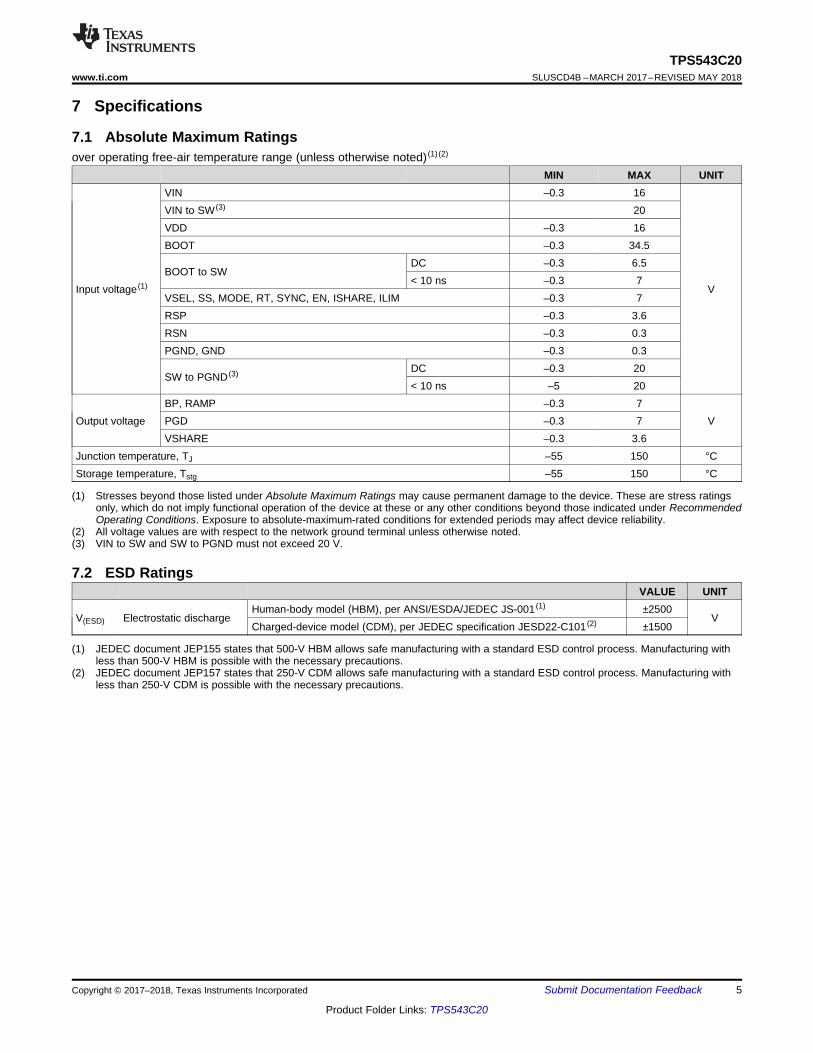
(1) Stresses beyond those listed under Absolute Maximum Ratings may cause permanent damage to the device. These are stress ratingsonly, which do not imply functional operation of the device at these or any other conditions beyond those indicated under RecommendedOperating Conditions. Exposure to absolute-maximum-rated conditions for extended periods may affect device reliability.
(2) All voltage values are with respect to the network ground terminal unless otherwise noted.(3) VIN to SW and SW to PGND must not exceed 20 V.
7 Specifications
7.1 Absolute Maximum Ratingsover operating free-air temperature range (unless otherwise noted) (1) (2)
MIN MAX UNIT
Input voltage (1)
VIN –0.3 16
V
VIN to SW (3) 20VDD –0.3 16BOOT –0.3 34.5
BOOT to SWDC –0.3 6.5< 10 ns –0.3 7
VSEL, SS, MODE, RT, SYNC, EN, ISHARE, ILIM –0.3 7RSP –0.3 3.6RSN –0.3 0.3PGND, GND –0.3 0.3
SW to PGND (3) DC –0.3 20< 10 ns –5 20
Output voltageBP, RAMP –0.3 7
VPGD –0.3 7VSHARE –0.3 3.6
Junction temperature, TJ –55 150 °CStorage temperature, Tstg –55 150 °C
(1) JEDEC document JEP155 states that 500-V HBM allows safe manufacturing with a standard ESD control process. Manufacturing withless than 500-V HBM is possible with the necessary precautions.
(2) JEDEC document JEP157 states that 250-V CDM allows safe manufacturing with a standard ESD control process. Manufacturing withless than 250-V CDM is possible with the necessary precautions.
7.2 ESD RatingsVALUE UNIT
V(ESD) Electrostatic dischargeHuman-body model (HBM), per ANSI/ESDA/JEDEC JS-001 (1) ±2500
VCharged-device model (CDM), per JEDEC specification JESD22-C101 (2) ±1500

6
TPS543C20SLUSCD4B –MARCH 2017–REVISED MAY 2018 www.ti.com
Product Folder Links: TPS543C20
Submit Documentation Feedback Copyright © 2017–2018, Texas Instruments Incorporated
(1) Stresses beyond those listed under may cause permanent damage to the device.(2) All voltage values are with respect to the network ground terminal unless otherwise noted.(3) See Layout Guidelines for VIN capacitor placement requirement to reduce MOSFET voltage stress.
7.3 Recommended Operating Conditionsover operating free-air temperature range (unless otherwise noted) (1)
MIN MAX UNIT
Input voltage (2)
VIN 4 14
V
VIN to SW (3) DC –0.1 18< 10 ns 18
VDD 4 16BOOT –0.1 23.5
BOOT to SWDC –0.1 5.5< 10 ns –0.1 6
VSEL, SS, MODE, RT, SYNC, EN, ISHARE,ILIM –0.1 5.5
RSP –0.1 1.7RSN –0.1 0.1PGND, GND –0.1 0.1
SW to PGNDDC –0.1 18< 10 ns –5 18
Outputvoltage (2)
BP, RAMP –0.3 7VPGD –0.3 7
VSHARE –0.3 3.6Junction temperature, TJ –40 125 °CStorage temperature, Tstg –55 125 °C
(1) For more information about traditional and new thermal metrics, see the Semiconductor and IC Package Thermal Metrics applicationreport, SPRA953.
7.4 Thermal Information
THERMAL METRIC (1)TPS543C20
UNITRVF (LQFN)40 PINS
RθJA Junction-to-ambient thermal resistance 28.9 °C/WRθJC(top) Junction-to-case (top) thermal resistance 18.9 °C/WRθJB Junction-to-board thermal resistance 4.1 °C/WψJT Junction-to-top characterization parameter 1.3 °C/WψJB Junction-to-board characterization parameter 4.1 °C/WRθJC(bot) Junction-to-case (bottom) thermal resistance 1 °C/W

7
TPS543C20www.ti.com SLUSCD4B –MARCH 2017–REVISED MAY 2018
Product Folder Links: TPS543C20
Submit Documentation FeedbackCopyright © 2017–2018, Texas Instruments Incorporated
(1) Specified by design. Not production tested.
7.5 Electrical Characteristicsover operating free-air temperature range (unless otherwise noted)
PARAMETER TEST CONDITIONS MIN TYP MAX UNITMOSFET RDS(ON)
RDS(on)HS HS FET VBST – VSW = 5 V, ID = 20 A, Tj = 25°C 3.0 mΩ
RDS(on)LS LS FET VDD = 5 V, ID = 20 A, Tj = 25°C 0.9 mΩ
tDEAD(LtoH)
Power stage driver dead-timefrom Low-side off to High-sideon (1)
VDD ≥ 12 V, TJ = 25°C 12 ns
tDEAD(HtoL)
Power stage driver dead-timefrom High-side off to Low-sideon (1)
VDDN ≥ 12 V, TJ = 25°C 15 ns
INPUT SUPPLY and CURRENTVVIN Power stage voltage 4 14VVDD VDD supply voltage 4 16
IVDD VDD bias current TA = 25°C, no load, power conversion enabled (noswitching) 4.3 mA
IVDDSTBY VDD standby current TA = 25°C, no load, power conversion disabled 4.3 mAUNDERVOLTAGE LOCKOUTVVDD_UVLO VDD UVLO rising threshold 3.8 VVVDD_UVLO_HYS VDD UVLO hysteresis 0.2 vVVIN_UVLO VIN UVLO rising threshold 3.2 VVVIN_UVLO_HYS VIN UVLO hysteresis 0.2 vVEN_ON_TH EN on threshold 1.45 1.6 1.75 VVHYS EN hysteresis 270 300 330 mVIEN_LKG EN input leakage current –1 0 1 µAINTERNAL REFERENCE VOLTAGEVINTREF Internal REF voltage RVSEL = OPEN 1000 mVVINTREFTOL Internal REF voltage tolerance TJ = -40°C to 125°C –0.5% +0.5%VINTREF_VSEL Internal REF voltage range Programable by VSEL (pin 36) 0.6 1.1 VOUTPUT VOLTAGEIRSP RSP input current VRSP= 600 mV –1 1 µADIFFERENTIAL REMOTE SENSE AMPLIFIERfUGBW Unity gain bandwidth (1) 5 8.5 MHzA0 Open loop gain (1) 75 dBSR SLew rate (1) ±10 V/µsVICM Input common mode range (1) –0.2 1.7 V
VOFFSET Input offset voltage (1) VRSN-VGND = 0 mV –1 1mV
VRSN-VGND = ±100 mV –1.9 1.9
8
TPS543C20SLUSCD4B –MARCH 2017–REVISED MAY 2018 www.ti.com
Product Folder Links: TPS543C20
Submit Documentation Feedback Copyright © 2017–2018, Texas Instruments Incorporated
Electrical Characteristics (continued)over operating free-air temperature range (unless otherwise noted)
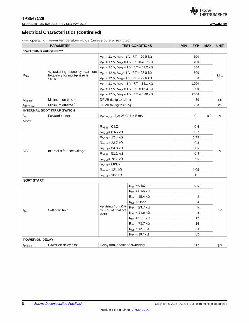
PARAMETER TEST CONDITIONS MIN TYP MAX UNITSWITCHING FREQUENCY
FSW
VO switching frequency maximumfrequency for multi-phase is1MHz
VIN = 12 V, VVO= 1 V, RT = 66.5 kΩ 300
kHz
VIN = 12 V, VVO = 1 V, RT = 48.7 kΩ 400VIN = 12 V, VVO = 1 V, RT = 39.2 kΩ 500VIN = 12 V, VVO= 1 V, RT = 28.0 kΩ 700VIN = 12 V, VVO= 1 V, RT = 22.6 kΩ 850VIN = 12 V, VVO = 1 V, RT = 19.1 kΩ 1000VIN = 12 V, VVO = 1 V, RT = 15.4 kΩ 1200VIN = 12 V, VVO = 1 V, RT = 8.06 kΩ 2000
tON(min) Minimum on-time (1) DRVH rising to falling 30 nstOFF(min) Minimum off-time (1) DRVH falling to rising 250 nsINTERNAL BOOTSTRAP SWITCHVF Forward voltage VBP-VBST, TA= 25°C, IF= 5 mA 0.1 0.2 VVSEL
VSEL Internal reference voltage
RVSEL= 0 kΩ 0.6
V
RVSEL= 8.66 kΩ 0.7RVSEL= 15.4 kΩ 0.75RVSEL= 23.7 kΩ 0.8RVSEL= 34.8 kΩ 0.85RVSEL= 51.1 kΩ 0.9RVSEL= 78.7 kΩ 0.95RVSEL= OPEN 1RVSEL= 121 kΩ 1.05RVSEL= 187 kΩ 1.1
SOFT START
tSS Soft-start timeVO rising from 0 Vto 95% of final setpoint
RSS = 0 kΩ 0.5
ms
RSS = 8.66 kΩ 1RSS = 15.4 kΩ 2RSS = Open 4RSS = 23.7 kΩ 5RSS = 34.8 kΩ 8RSS = 51.1 kΩ 12RSS = 78.7 kΩ 16RSS = 121 kΩ 24RSS = 187 kΩ 32
POWER ON DELAYtPODLY Power-on delay time Delay from enable to switching 512 µs

9
TPS543C20www.ti.com SLUSCD4B –MARCH 2017–REVISED MAY 2018
Product Folder Links: TPS543C20
Submit Documentation FeedbackCopyright © 2017–2018, Texas Instruments Incorporated
Electrical Characteristics (continued)over operating free-air temperature range (unless otherwise noted)
PARAMETER TEST CONDITIONS MIN TYP MAX UNITPGOOD COMPARATOR
VPG(thresh)
OV warning threshold on RSPpin, PGOOD fault threshold onrising
VREF = 600 mV 108 112 116
%VREFUV warning threshold on RSPpin, PGOOD fault threshold onfalling
VREF = 600 mV 84 88 92
VPGD(rise)
PGOOD threshold on rising andUV warning threshold de-assertion threshold at RSP pin
VREF = 600 mV 95 %VREF
VPGD(fall)
PGOOD threshold on falling andOV warning threshold de-assertion threshold at RSP pin
VREF = 600 mV 105 %VREF
RPGD PGOOD pulldown resistance IPGOOD = 5 mA, VRSP = 0 V 30 45 60 Ω
tPGDLY PGOOD delay timeDelay for PGOOD going in 1.024 msDelay for PGOOD coming out 2 µs
VPGD(OL)PGOOD output low level voltageat no supply voltage VDD=0, IPGOOD = 80 µA 0.8 V
IPGLK PGOOD leakage current VPGOOD = 5 V 15 µACURRENT SHARE ACCURACY
ISHARE(acc)
Output current sharing accuracyamong stackable devices, definedas the ratio of the currentdifference between devices tototal current(sensing error only) (1)
IOUT ≥ 20 A/phase –15% 15%
IOUT ≤ 20 A/phase ±3 A
CURRENT DETECTIONVILIM VTRIP voltage range Rdson sensing 0.1 1.2 V
IOCPLow-side FET current protectionthreshold and tolerance
RILIM= 33.2 kΩ 35 AOC tolerance ±10%
IOCPLow-Side FET Current protectionthreshold and tolerance
RILIM= 23.7 kΩ 25 AOC tolerance ±15%
IOCP_N Negative current limit threshold Valley-point current sense –23 A
ICLMP_LOClamp current at VTRIP clamp atlowest 25°C, VTRIP = 0.1 V 5.5 6.5 7.5 A

10
TPS543C20SLUSCD4B –MARCH 2017–REVISED MAY 2018 www.ti.com
Product Folder Links: TPS543C20
Submit Documentation Feedback Copyright © 2017–2018, Texas Instruments Incorporated
Electrical Characteristics (continued)over operating free-air temperature range (unless otherwise noted)
PARAMETER TEST CONDITIONS MIN TYP MAX UNITHIGH-SIDE SHORT-CIRCUIT PROTECTION
IHSOCHigh-side short circuit protectionfault threshold (1) 60 A
OV / UV PROTECTIONVOVP OVP threshold voltage OVP detect voltage 113 117 121 %VREFtOVPDLY OVP response time (1) OVP response time with 100-mV overdrive 1 µsVUVP UVP threshold voltage UVP detect voltage 79 83 87 %VREFtUVPDLY UVP delay (1) UVP delay 1.5 µstHICDLY Hiccup delay time Regular tSS setting 7 × tSS msBP LDO REGULATORBP LDO output voltage VIN = 12 V, ILOAD = 0 to 10 mA 4.5 5 5.5 V
VBPUVLO BP UVLO threshold voltageWakeup 3.32
VShutdown 3.11
VLDOBP LDO low dropout voltage VIN= 4.5 V, ILOAD= 30 mA, TA = 25°C 365 mVILDOMAX LDO overcurrent limit VIN= 12 V, TA = 25°C 100 mASYNCHRONIZATIONVIH(SYNC) High-level input voltage 2
VVIL(SYNC) Low-level input voltage 0.8tPSW(SYNC) Sync input minimum pulse width 100 ns
FSYNCSynchronization frequency 300 2000
kHzDual-phase 300 1000
tSYNC to SW
Sync to SW delay tolerance,percentage from phase-to-phase (1)
FSYNC = 300 kHz to 1 MHz, 10%
tLose_SYNC_delay Delay when lose sync clock (1) FSYNC = 300 kHz 5 µsTHERMAL SHUTDOWN
TSDNBuilt-in thermal shutdownthreshold (1)
Shutdown temperature 155 165°C
Hysteresis 30

Output Current (A)
Effi
cien
cy (
%)
0 5 10 15 20 25 30 35 4060%
70%
80%
90%
100%
D020
14 VIN12 VIN9 VIN5 VIN4 VIN
Output Current (A)
Pow
er L
oss
(W)
0 5 10 15 20 25 30 35 400
1
2
3
4
5
6
7
8
9
D021
14 VIN12 VIN9 VIN5 VIN4 VIN
Output Current (A)
Effi
cien
cy (
%)
0 5 10 15 20 25 30 35 4060%
65%
70%
75%
80%
85%
90%
95%
100%
D016
5 VOUT3.3 VOUT
2.5 VOUT1.5 VOUT
1 VOUT0.6 VOUT
Output Current (A)
Pow
er L
oss
(W)
0 5 10 15 20 25 30 35 400
1
2
3
4
5
6
7
8
9
D017
5 VOUT3.3 VOUT2.5 VOUT1.5 VOUT1 VOUT0.6 VOUT
Output Current (A)
Effi
cien
cy (
%)
0 5 10 15 20 25 30 35 4060%
65%
70%
75%
80%
85%
90%
95%
100%
D012
3.3 VOUT2.5 VOUT
1.5 VOUT1 VOUT
0.6 VOUT
Output Current (A)
Pow
er L
oss
(W)
0 5 10 15 20 25 30 35 400
1
2
3
4
5
6
7
8
9
10
D013
3.3 VOUT2.5 VOUT1.5 VOUT1 VOUT0.6 VOUT
11
TPS543C20www.ti.com SLUSCD4B –MARCH 2017–REVISED MAY 2018
Product Folder Links: TPS543C20
Submit Documentation FeedbackCopyright © 2017–2018, Texas Instruments Incorporated
7.6 Typical CharacteristicsVIN = VDD = 12 V, TA = 25°C, RRT = 40.2 kΩ, TA= 25°C (unless otherwise specified)
VIN = 5 V 500 kHz 25°C
Figure 1. Efficiency vs Output Current
VIN = 5 V 500 kHz 25°C
Figure 2. Power Loss vs Output Current
VIN = 12 V 500 kHz 25°C
Figure 3. Efficiency vs Output Current
VIN = 12 V 500 kHz 25°C
Figure 4. Power Loss vs Output Current
VOUT = 1 V 1 MHz 25°C
Figure 5. Efficiency vs Output Current
VOUT = 1 V 1 MHz 25°C
Figure 6. Power Loss vs Output Current

Output Current (A)
Out
put V
olta
ge (
V)
0 5 10 15 20 25 30 35 400.95
1
1.05
D019
14 VIN12 VIN9 VIN5 VIN4 VIN
Output Current (A)
Out
put V
olta
ge (
V)
0 5 10 15 20 25 30 35 400
1
2
3
4
5
6
D007D007
0.6 VOUT1 VOUT
1.5 VOUT2.5 VOUT
3.3 VOUT5 VOUT
Output Current (A)
Fre
quen
cy (
KH
z)
0 5 10 15 20 25 30 35 40200
300
400
500
600
700
800
D010
0.6 VOUT1 VOUT1.5 VOUT2.5 VOUT3.3 VOUT5 VOUT
12
TPS543C20SLUSCD4B –MARCH 2017–REVISED MAY 2018 www.ti.com
Product Folder Links: TPS543C20
Submit Documentation Feedback Copyright © 2017–2018, Texas Instruments Incorporated
Typical Characteristics (continued)VIN = VDD = 12 V, TA = 25°C, RRT = 40.2 kΩ, TA= 25°C (unless otherwise specified)
VIN = 12 V 500 kHz 25°C
Figure 7. Output Voltage vs Output Current
VIN = 12 V 500 kHz 25°C
Figure 8. Switching Frequency vs Output Current
VOUT = 1 V 1 MHz 25°C
Figure 9. Output Voltage vs Output CurrentFigure 10. Start-Up From EN
Figure 11. Output Voltage Start-Up and Shutdown Figure 12. Output Voltage Ripple at Steady State

13
TPS543C20www.ti.com SLUSCD4B –MARCH 2017–REVISED MAY 2018
Product Folder Links: TPS543C20
Submit Documentation FeedbackCopyright © 2017–2018, Texas Instruments Incorporated
Typical Characteristics (continued)VIN = VDD = 12 V, TA = 25°C, RRT = 40.2 kΩ, TA= 25°C (unless otherwise specified)
15 A to 25 A to 15 A, 10-A Step at 40 A/µs
Figure 13. Output Voltage Transient Response

Stacked NexFET
Power Stage
BP
Driver
Control:
Anti-Cross-
Conduction,
Prebias
S Q
ROscillator
PWM
Overcurrent
Detection ,
Current sensing
OC
Th
res
ho
ld
SYNC
Average Iout
OC Event
EN
SS
PVIN
BOOT
SW
Fault
PGND
Linear Regulators
BP
BP3
RSP
RSN
RAMP
ISHARE
VDD
RT
BP
API
REMOTE SENSE AMP
VSHARE
GND
PGD
ACM Controller
Phase Managment
Phase
Balance
Start and Reference
Re
fere
nc
e
Fault
Control
ILIM
MODE
VSEL
AGND
Copyright © 2017, Texas Instruments Incorporated
14
TPS543C20SLUSCD4B –MARCH 2017–REVISED MAY 2018 www.ti.com
Product Folder Links: TPS543C20
Submit Documentation Feedback Copyright © 2017–2018, Texas Instruments Incorporated
8 Detailed Description
8.1 OverviewThe TPS543C20 device is 40-A, high-performance, synchronous buck converter with two integrated N-channelNexFET™ power MOSFETs. These devices implement the fixed frequency non-compensation mode control.Safe pre-bias capability eliminates concerns about damaging sensitive loads. Two TPS543C20 devices can beparalleled together to provide up to 80-A load. Current sensing for over-current protection and current sharingbetween devices is done by sampling a small portion of the power stage current providing accurate informationindependent on the device temperature.
Advanced Current Mode (ACM) is an emulated peak current control topology. It supports stable static andtransient operation without complex external compensation design. This control architecture includes an internalramp generation network that emulates inductor current information, enabling the use of low ESR outputcapacitors such as multi-layered ceramic capacitors (MLCC). The internal ramp also creates a high signal tonoise ratio for good noise immunity. The TPS543C20 has 10 ramp options (see Ramp Selections for detail) tooptimize internal loop for various inductor and output capacitor combinations with only a simple resistor to GND.The TPS543C20 is easy to use and allows low external component count with fast load transient response.Fixed-frequency modulation also provides ease-of-filter design to overcome EMI noise.
8.2 Functional Block Diagram
15
TPS543C20www.ti.com SLUSCD4B –MARCH 2017–REVISED MAY 2018
Product Folder Links: TPS543C20
Submit Documentation FeedbackCopyright © 2017–2018, Texas Instruments Incorporated
8.3 Feature DescriptionThe TPS543C20 device is a high-performance, integrated FET converter supporting current rating up to 40-Athermally. It integrates two N-channel NexFET™ power MOSFETs, enabling high power density and small PCBlayout area. The drain-to-source breakdown voltage for these FETs is 20 V DC and transient. Avalanchebreakdown occurs if the absolute maximum voltage rating exceeds 20 V. In order to limit the switch node ringingof the device, TI recommends adding a R-C snubber from the SW node to the PGND pins. Also a 10~100nFcapacitor from VIN (Pin 25) to GND (Pin2 7) is mandatory to reduce high side FET stress. Refer to LayoutGuidelines for the detailed recommendations.
The typical on-resistance (RDS(on)) for the high-side MOSFET is 3 mΩ and typical on-resistance for the low-sideMOSFET is 0.9 mΩ with a nominal gate voltage (VGS) of 5 V.
8.4 Device Functional Modes
8.4.1 Soft-Start OperationIn the TPS543C20 device, the soft-start time controls the inrush current required to charge the output capacitorbank during start-up. The device offers 10 selectable soft-start options ranging from 0.5 ms to 32 ms. When thedevice is enabled the reference voltage ramps from 0 V to the final level defined by VSEL pin strap configuration,in a given soft-start time, which can be selected by SS pin. See Table 1 for details.
(1) The E48 series resistors with no more than 1% tolerance are recommended.
Table 1. SS Pin ConfigurationSS TIME (ms) RESISTOR VALUE (kΩ) (1)
0.5 01 8.662 15.45 23.74 OPEN8 34.812 51.116 78.724 12132 187
8.4.2 Input and VDD Undervoltage Lockout (UVLO) ProtectionThe TPS543C20 provides fixed VIN and VDD undervoltage lockout threshold and hysteresis. The typical VINturnon threshold is 3.2 V and hysteresis is 0.2 V. The typical VDD turnon threshold is 3.8 V and hysteresis is0.2 V. No specific power-up sequence is required.
8.4.3 Power Good and EnableThe TPS543C20 has power-good output that indicates logic high when output voltage is within the target. Thepower-good function is activated after soft-start has finished. When the soft-start ramp reaches 90% of setpoint,PGOOD detection function will be enabled. If the output voltage becomes within ±8% of the target value, internalcomparators detect power-good state and the power good signal becomes high after a delay. If the outputvoltage goes outside of ±12% of the target value, the power good signal becomes low after an internal delay.The power-good output is an open-drain output and must be pulled up externally.
This part has internal pull up for EN. EN is internally pulled up to BP when EN pin is floating. EN can be pulledlow through external grounding. When EN pin voltage is below its threshold, TPS543C20 enters into shutdownoperation, and the minimum time for toggle EN to reset is 5 µs.

RRAMP
CRAMPRAMP
Duty Cycle
RAMP
SLOPESlope
Compensation
10 Selections
16
TPS543C20SLUSCD4B –MARCH 2017–REVISED MAY 2018 www.ti.com
Product Folder Links: TPS543C20
Submit Documentation Feedback Copyright © 2017–2018, Texas Instruments Incorporated
8.4.4 Voltage ReferenceVSEL pin strap is used to program initial boot voltage value from 0.6 V to 1.1 V by the resistor connected fromVSEL to AGND. The initial boot voltage is used to program the main loop voltage reference point. VSEL voltagesettings provide TI designated discrete internal reference voltages. Table 2 lists internal reference voltageselections.
(1) The E48 series resistors with no worse than 1% tolerance arerecommended
Table 2. VSEL Pin ConfigurationDEFAULT Vref (V) RESISTOR VALUE (kΩ) (1)
0.6 00.7 8.660.75 15.40.8 23.70.85 34.80.9 51.10.95 78.71.0 OPEN1.05 1211.1 187
8.4.5 Prebiased Output Start-upThe device prevent current from being discharged from the output during start-up, when a pre-biased outputcondition exists. No SW pulses occur until the internal soft-start voltage rises above the error amplifier inputvoltage, if the output is pre-biased. As soon as the soft-start voltage exceeds the error amplifier input, and SWpulses start, the device limits synchronous rectification after each SW pulse with a narrow on-time. The low-sideMOSFET on-time slowly increases on a cycle-by-cycle basis until 128 pulses have been generated and thesynchronous rectifier runs fully complementary to the high-side MOSFET. This approach prevents the sinking ofcurrent from a pre-biased output, and ensures the output voltage start-up and ramp-to regulation sequences aresmooth and monotonic.
8.4.6 Internal Ramp GeneratorInternal ramp voltage is generated from duty cycle that contains emulated inductor ripple current information andthen feed it back for control loop regulation and optimization according to required output power stage, duty ratioand switching frequency. Internal ramp amplitude is set by RAMP pin by adjusting an internal ramp generationcapacitor CRAMP, selected by the resistor connected from MODE pin to GND. For best performance, werecommend ramp signal to be no more than 4 times of output ripple signal for all Low ESR output capacitor(MLCC) applications, or no more than 2 times larger than output ripple signal for regular ESR output capacitor(Pos-cap) applications. For design recommendation, please find the design tool at www.ti.com/WEBENCH.
Figure 14. Internal Ramp Generator
TPS543C20
RT SYNC
Master
MODE
17
TPS543C20www.ti.com SLUSCD4B –MARCH 2017–REVISED MAY 2018
Product Folder Links: TPS543C20
Submit Documentation FeedbackCopyright © 2017–2018, Texas Instruments Incorporated
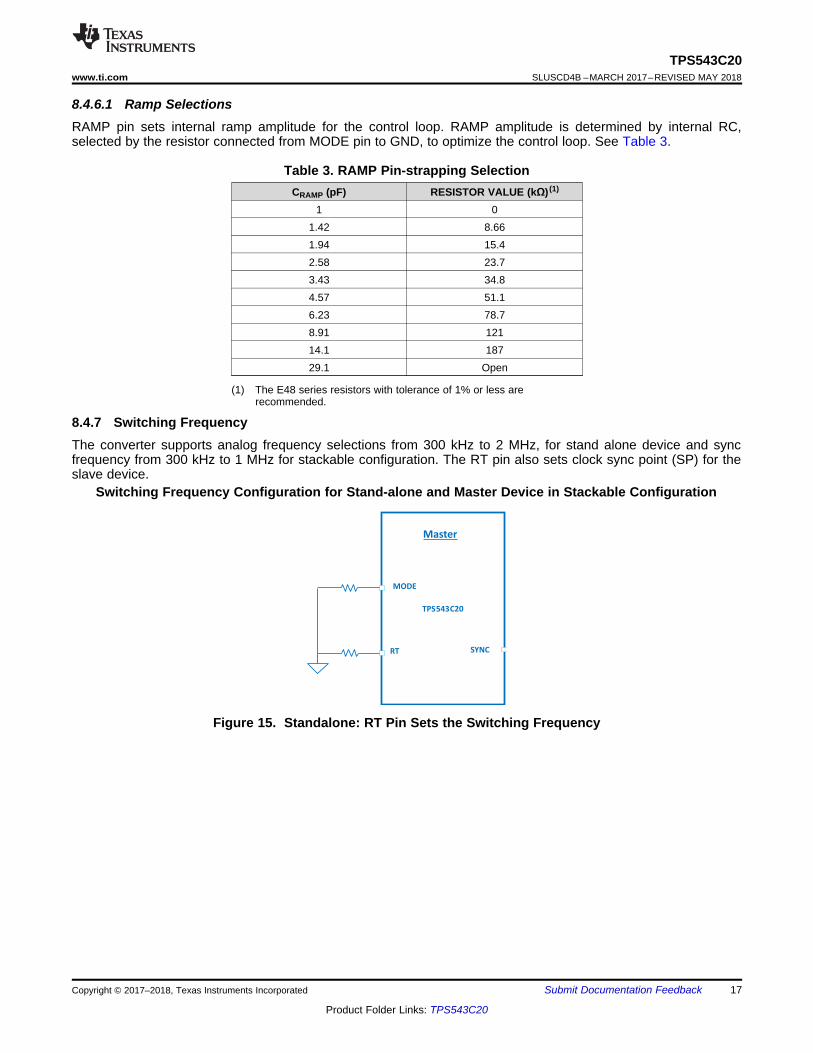
8.4.6.1 Ramp SelectionsRAMP pin sets internal ramp amplitude for the control loop. RAMP amplitude is determined by internal RC,selected by the resistor connected from MODE pin to GND, to optimize the control loop. See Table 3.
(1) The E48 series resistors with tolerance of 1% or less arerecommended.
Table 3. RAMP Pin-strapping SelectionCRAMP (pF) RESISTOR VALUE (kΩ) (1)
1 01.42 8.661.94 15.42.58 23.73.43 34.84.57 51.16.23 78.78.91 12114.1 18729.1 Open
8.4.7 Switching FrequencyThe converter supports analog frequency selections from 300 kHz to 2 MHz, for stand alone device and syncfrequency from 300 kHz to 1 MHz for stackable configuration. The RT pin also sets clock sync point (SP) for theslave device.
Switching Frequency Configuration for Stand-alone and Master Device in Stackable Configuration
Figure 15. Standalone: RT Pin Sets the Switching Frequency
0
1/2
System Clock
or
Master Clock
Slave clock
1/2
0
¦ ´´-
¦
9
SWRT
SW
220 10R =
2000
RT SYNC
Master
MODE
RTSYNC
Slave
MODE
ISHARE ISHARE
VSHARE VSHARE
18
TPS543C20SLUSCD4B –MARCH 2017–REVISED MAY 2018 www.ti.com
Product Folder Links: TPS543C20
Submit Documentation Feedback Copyright © 2017–2018, Texas Instruments Incorporated
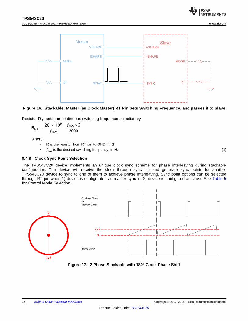
Figure 16. Stackable: Master (as Clock Master) RT Pin Sets Switching Frequency, and passes it to Slave
Resistor RRT sets the continuous switching frequence selection by
where• R is the resistor from RT pin to GND, in Ω• ƒSW is the desired switching frequency, in Hz (1)
8.4.8 Clock Sync Point SelectionThe TPS543C20 device implements an unique clock sync scheme for phase interleaving during stackableconfiguration. The device will receive the clock through sync pin and generate sync points for anotherTPS543C20 device to sync to one of them to achieve phase interleaving. Sync point options can be selectedthrough RT pin when 1) device is configurated as master sync in, 2) device is configured as slave. See Table 5for Control Mode Selection.
Figure 17. 2-Phase Stackable with 180° Clock Phase Shift

RT
F_SW
SYNC
Master
MODE
23.7 k
RT
OpenSync Point
SYNC
Slave
MODE
51.1 k
ISHARE ISHARE
VSHARE VSHARE
19
TPS543C20www.ti.com SLUSCD4B –MARCH 2017–REVISED MAY 2018
Product Folder Links: TPS543C20
Submit Documentation FeedbackCopyright © 2017–2018, Texas Instruments Incorporated
Table 4. RT Pin Sync Point SelectionCLOCK SYNC OPTIONS RESISTOR VALUE (kΩ)
0 (0° Interleaving) 01/4 (90° Interleaving) 8.661/3 (120° Interleaving) 15.42/3 (240° Interleaving) 23.73/4 (270° Interleaving) 34.81/2 (180° Interleaving) OPEN
8.4.9 Synchronization and Stackable ConfigurationThe TPS543C20 device can synchronize to an external clock which must be equal to or higher than internalfrequency setting. For stand alone device, the external clock should be applied to the SYNC pin. A suddenchange in synchronization clock frequency causes an associated control loop response, resulting in an overshootor undershoot on the output voltage.
In dual phase stackable configuration:1. when there is no external system clock applied, the master device will be configured as clock master,
sending out pre-set switching frequency clock to slave device through SYNC pin. Slave will receive this clockas switching clock with phase interleaving.
2. when a system clock is applied, both master and slave devices will be configured as clock slave, they willsync to the external system clock as switching frequency with proper phase shift
8.4.10 Dual-Phase Stackable Configurations
8.4.10.1 Configuration 1: Master Sync Out Clock-to-Slave• Direct SYNC, VSHARE and ISHARE connections between Master and Slave.• Switching frequency is set by RT pin of Master, and pass to slave through SYNC pin. SYNC pin of master will
be configured as sync out by it’s MODE pin.• Slave receives clock from SYNC pin. It’s RT pin determines the sync point for clock phase shift.
Figure 18. 2-Phase Stackable with 180° Phase Shift: Master Sync Out Clock-to-Slave
8.4.10.2 Configuration 2: Master and Slave Sync to External System Clock• Direct connection between external clock and SYNC pin of Master and Slave.• Direct VSHARE and ISHARE connections between Master and Slave.• SYNC pin of master will be configured as sync in by it’s MODE pin.• Master and Slave receive external system clock from SYNC pin. Their RT pin determine the sync point for
clock phase shift.

RT0 k
Sync Point
SYNC
Master
MODE34.8 k
RT
OpenSync Point
SYNC
Slave
MODE
51.1 k
ISHARE ISHARE
VSHARE VSHARE
System Clock
20
TPS543C20SLUSCD4B –MARCH 2017–REVISED MAY 2018 www.ti.com
Product Folder Links: TPS543C20
Submit Documentation Feedback Copyright © 2017–2018, Texas Instruments Incorporated
(1) The E48 series resistors with tolerance of 1% or less are recommended.
Figure 19. 2-Phase Stackable with 180° Phase Shift: Master and Slave Sync to External System Clock
8.4.11 Operation ModeThe operation mode and API/Body Brake feature is set by the MODE pin. They are selected by the resistorconnected from MODE pin to GND. Mode pin sets the device to be stand-alone mode or stackable mode. Instand-alone mode, MODE pin sets the API on/off or trigger point sensitivity of API (1x stands for most sensitiveand 4x stands for least sensitive). In stackable mode, the MODE pin sets the device as master or slave, as wellas SYNC pin function (sync in or sync out) of the master device.
Table 5. MODE Pin-Strapping SelectionCONTROL MODE
SELECTION API/BODY BRAKE RESISTOR VALUE (kΩ) and API/BBThreshold (1) NOTE
StandaloneAPI/body brake
API OFFBB OFF Open
• Sync pin to receive clock• RT pin to set frequency
API ONBB OFF 15.4, API = 35 mV
API ONBB ON
(API Threshold Setting)
121, API = 15 mV, BB = 30 mV187, API = 25 mV, BB = 30 mV8.66, API = 35 mV, BB = 30 mV78.7, API = 45 mV, BB = 30 mV
(Master sync out)
API OFFBB OFF
23.7 • Sync pin to send out clock• RT pin to set frequency
(Master sync in) 34.8 • Sync pin to receive clock• RT pin to set sync point
(Slave Sync In) 51.1 • Sync pin to receive clock• RT pin to set sync point
8.4.12 API/BODY BrakeTPS543C20 is a true fixed frequency converter. The major limitation for any fixed frequency converter is thatduring transient load step up, the converter needs to wait for the next clock cycle to response to the load change,depending on loop bandwidth design and the timing of load transient, this delay time could cause additionaloutput voltage drop. TPS543C20 implements a special circuitry to improve transient performance. During loadstep up, the converter senses both the speed and the amplitude of the output voltage change, if the outputvoltage change is fast and big enough, the converter will issue an additional PWM pulse before the nextavailable clock cycle to stop output voltage from further dropping, thus reducing the undershoot voltage.

OCP ILIM DS(on) IND(ripple)
IN OUT OUTILIM
DS(on) SW IN
I = V (16 × R ) - I 2
(V - V ) × VV 1= - ×
16 × R 2 × L × ƒ V
: u PILIM ILIM ILIMV mV R (k ) I ( A)
Vout ± Body Brake disabledVout ± Body Brake enabled
LOAD
Switch Node
Vout ± API disabledVout ± API enabled
LOAD
Switch Node
21
TPS543C20www.ti.com SLUSCD4B –MARCH 2017–REVISED MAY 2018
Product Folder Links: TPS543C20
Submit Documentation FeedbackCopyright © 2017–2018, Texas Instruments Incorporated
During load step down, TPS543C20 implements a body brake function, that turns off both high-side and lowsideFET, and allows power to dissipate through the low-side body diode, reducing overshoot. This approach is veryeffective while having some impact on efficiency during transient. See Figure 20 and Figure 21.
Figure 20. Undershoot Comparison with API ON/OFF Figure 21. Overshoot Comparison with Body BrakeON/OFF
8.4.13 Sense and Overcurrent Protection
8.4.13.1 Low-Side MOSFET Overcurrent ProtectionThe TPS543C20 utilizes ILIM pin to set the OCP level. The ILIM pin should be connected to AGND through theILIM voltage setting resistor, RILIM. The ILIM terminal sources IILIM current, which is around 11.2 μA typically atroom temperature, and the ILIM level is set to the OCP ILIM voltage VILIM as shown in Equation 2. In order toprovide both good accuracy and cost effective solution, TPS543C20 supports temperature compensatedMOSFET RDS(on) sensing.
Consider RDS(on) variation vs VDD in calculation (2)
Also, TPS543C20 performs both positive and fixed negative inductor current limiting.
The inductor current is monitored by the voltage between GND pin and SW pin during the OFF time. ILIM has1200 ppm/°C temperature slope to compensate the temperature dependency of the RDS(on). The GND pin is usedas the positive current sensing node.
The device has cycle-by-cycle over-current limiting control. The inductor current is monitored during the OFFstate and the controller maintains the OFF state during the period that the inductor current is larger than theovercurrent ILIM level. VILIM sets the Peak level of the inductor current. Thus, the load current at the overcurrentthreshold, IOCP, can be calculated as shown in .
where• RDS(on) is the on-resistance of the low-side MOSFET. (3)
Equation 3 is valid for VDD ≥ 5 V. Use 0.58 mΩ for RDS(on) in calculation, which is the pure on-resistance forcurrent sense.

22
TPS543C20SLUSCD4B –MARCH 2017–REVISED MAY 2018 www.ti.com
Product Folder Links: TPS543C20
Submit Documentation Feedback Copyright © 2017–2018, Texas Instruments Incorporated
If an overcurrent event is detected in a given switching cycle, the device increments an overcurrent counter.When the device detects three consecutive overcurrent (either high-side or low-side) events, the converterresponds, entering continuous restart hiccup. In continuous hiccup mode, the device implements a 7 soft-startcycle timeout, followed by a normal soft-start attempt. When the overcurrent fault clears, normal operationresumes; otherwise, the device detects overcurrent and the process repeats.
8.4.13.2 High-Side MOSFET Overcurrent ProtectionThe device also implements a fixed high-side MOSFET overcurrent protection to limit peak current, and preventinductor saturation in the event of a short circuit. The device detects an overcurrent event by sensing the voltagedrop across the high-side MOSFET during ON state. If the peak current reaches the IHOSC level on any givencycle, the cycle terminates to prevent the current from increasing any further. High-side MOSFET overcurrentevents are counted. If the devices detect three consecutive overcurrent events (high-side or low-side), theconverter responds by entering continuous restart hiccup.
8.4.14 Output Overvoltage and Undervoltage ProtectionThe device includes both output overvoltage protection and output undervoltage protection capability. Thedevices compare the RSP pin voltage to internal selectable pre-set voltages. If the RSP voltage with respect toRSN voltage rises above the output overvoltage protection threshold, the device terminates normal switching andturns on the low-side MOSFET to discharge the output capacitor and prevent further increases in the outputvoltage. Then the device enters continuous restart hiccup.
If the RSP pin voltage falls below the undervoltage protection level, after soft-start has completed, the deviceterminates normal switching and forces both the high-side and low-side MOSFETs off, then enters hiccup time-out delay prior to restart.
8.4.15 Overtemperature ProtectionAn internal temperature sensor protects the devices from thermal runaway. The internal thermal shutdownthreshold, TSD, is fixed at 165°C typical. When the devices sense a temperature above TSD, power conversionstops until the sensed junction temperature falls by the thermal shutdown hysteresis amount; then, the devicestarts up again.
8.4.16 RSP/RSN Remote Sense FunctionRSP and RSN pins are used for remote sensing purpose. In the case where feedback resistors are required foroutput voltage programming, the RSP pin should be connected to the mid-point of the resistor divider and theRSN pin should always be connected to the load return.
In the case where feedback resistors are not required as when the VSEL programs the output voltage set point,the RSP pin should be connected to the positive sensing point of the load and the RSN pin should always beconnected to the load return. RSP and RSN pins are extremely high-impedance input terminals of the truedifferential remote sense amplifier. The feedback resistor divider should use resistor values much less than 100kΩ. A simple rule of thumb is to use a 10-kΩ lower divider resistor and then size the upper resistor to achieve thedesired ratio.

Tp
Tp
Declare fault and take action
Sync fault delay
Switching pulses
TdelayTp +
TPS543C20
RSP
RSN2
1
+ –
Load
5
BOOT
Copyright ©2017, Texas Instruments Incorporated
TPS543C20
RSP
RSN2
1
+ –
Load
5
BOOT
Copyright ©2017, Texas Instruments Incorporated
23
TPS543C20www.ti.com SLUSCD4B –MARCH 2017–REVISED MAY 2018
Product Folder Links: TPS543C20
Submit Documentation FeedbackCopyright © 2017–2018, Texas Instruments Incorporated
Figure 22. Remote Sensing With Feedback Resistors Figure 23. Remote Sensing Without Feedback Resistors
8.4.17 Current SharingWhen devices operate in dual-phase stackable application, a current sharing loop maintains the current balancebetween devices. Both devices share the same internal control voltage through VSHARE pin. The sensedcurrent in each phase is compared first in a current share block by connecting ISHARE pin of each device, thenthe error current is added into the internal loop. The resulting voltage is compared with the PWM ramp togenerate the PWM pulse.
8.4.18 Loss of SynchronizationDuring sync clock condition, each individual converter will continuously compare current falling edge andprevious falling edge, if current falling edge exceeded a 1us delay versus previous pulse, converter will declare alost sync fault, and response by pulling down ISHARE to shut down all phases.
Figure 24. Switching Response When Sync Clock Lost

PVIN
PGOOD
EN
1817
1615
1413
1110987654321
3334
3536
3738
39
212223242526272829303132
PV
IN
PV
IN
PV
IN
PV
IN
PV
IN
SW
SW
SW
SW
SW
BO
OT
PGND
PGND
PGND
PGND
PGND
PGND
PGND
PGD
VD
D
EN
RAMP
BP
40
12
PGND
2019
Thermal Tab
ILIM
GN
D
RS
N
RS
P
SS
RT
SYNC
MODE
VS
HA
RE
ISH
AR
E
NC
NC
NC
NC
AG
ND
VSEL
+-
LOAD
24
TPS543C20SLUSCD4B –MARCH 2017–REVISED MAY 2018 www.ti.com
Product Folder Links: TPS543C20
Submit Documentation Feedback Copyright © 2017–2018, Texas Instruments Incorporated
9 Application and Implementation
NOTEInformation in the following applications sections is not part of the TI componentspecification, and TI does not warrant its accuracy or completeness. TI’s customers areresponsible for determining suitability of components for their purposes. Customers shouldvalidate and test their design implementation to confirm system functionality.
9.1 Application InformationThe TPS543C20 device is a highly-integrated synchronous step-down DC/DC converter. The device is used toconvert a higher DC input voltage to a lower DC output voltage, with a maximum output current of 40 A. Use thefollowing design procedure to select key component values for this device.
9.2 Typical Application: TPS543C20 Stand-alone Device
Figure 25. 4.5-V to 16-V Input, 1-V Output, 40-A Converter

25
TPS543C20www.ti.com SLUSCD4B –MARCH 2017–REVISED MAY 2018
Product Folder Links: TPS543C20
Submit Documentation FeedbackCopyright © 2017–2018, Texas Instruments Incorporated
(1) Recommended electrical ratings:(a) Input voltage ≤ 7 V: current rating ≤ 40 A(b) Input voltage ≤ 11 V: current rating ≤ 35 A(c) Input voltage ≤ 14 V: current rating ≤ 30 A
(2) DC overcurrent level
9.2.1 Design RequirementsFor this design example, use the input parameters shown in Table 6.
Table 6. Design Example SpecificationsPARAMETER TEST CONDITION MIN TYP MAX UNIT
VIN Input voltage (1) 4 12 14 VVIN(ripple) Input ripple voltage IOUT = 40 A 0.4 VVOUT Output voltage 0.9 V
Line regulation 5 V ≤ VIN ≤ 14 V 0.5%Load regulation 0 V ≤ IOUT ≤ 40 A 0.5%
VPP Output ripple voltage IOUT = 40 A 20 mVVOVER Transient response overshoot ISTEP = 10 A 50 mVVUNDER Transient response undershoot ISTEP = 10A 50 mVIOUT Output current 5 V ≤ VIN ≤ 16 V 35 40 AtSS Soft-start time VIN = 12 V 4 msIOC Overcurrent trip point (2) 45 Aη Peak efficiency IOUT = 20 A, VIN = 12 V, VDD = 5 V 90%fSW Switching frequency 300 500 700 kHz
9.2.2 Detailed Design Procedure
9.2.2.1 Custom Design With WEBENCH® ToolsClick here to create a custom design using the TPS543C20 device with the WEBENCH® Power Designer.1. Start by entering the input voltage (VIN), output voltage (VOUT), and output current (IOUT) requirements.2. Optimize the design for key parameters such as efficiency, footprint, and cost using the optimizer dial.3. Compare the generated design with other possible solutions from Texas Instruments.
The WEBENCH Power Designer provides a customized schematic along with a list of materials with real-timepricing and component availability.
In most cases, these actions are available:• Run electrical simulations to see important waveforms and circuit performance• Run thermal simulations to understand board thermal performance• Export customized schematic and layout into popular CAD formats• Print PDF reports for the design, and share the design with colleagues
Get more information about WEBENCH tools at www.ti.com/WEBENCH.
9.2.2.2 Switching Frequency SelectionSelect a switching frequency for the TPS543C20. There is a trade off between higher and lower switchingfrequencies. Higher switching frequencies may produce smaller solution size using lower valued inductors andsmaller output capacitors compared to a power supply that switches at a lower frequency. However, the higherswitching frequency causes extra switching losses, which decrease efficiency and impact thermal performance.In this design, a moderate switching frequency of 500 kHz achieves both a small solution size and a highefficiency operation is selected. The device supports continuous switching frequency programming; seeEquation 4. additional considerations (internal ramp compensation) other than switching frequency need to beincluded.

ESRCIN (max ) =VRIPPLE(ESR)
IOUT :max ; + @IRIPPLE
2A
= 7 m3
CIN (min ) =IOUT (max ) × VOUT
VRIPPLE :cap ; × VIN:max ; × fSW
= 38.5 JF
( )IN OUTOUTCIN(rms) OUT(max)
IN IN
V -VVI = I = 16 Arms
V V´ ´
OUT IN OUT
IN SW OUT
V V V 1 V (12 V - 1V)L = = 458 nH
V ƒ I KIND 12 V 500 kHz 40 A 0.1
- ´
- =
´ ´ ´ ´ ´
9 3
RT 3
20 10 500 10R = 2 39.5 k
2000500 10
´ ´- ´ = W
´
26
TPS543C20SLUSCD4B –MARCH 2017–REVISED MAY 2018 www.ti.com
Product Folder Links: TPS543C20
Submit Documentation Feedback Copyright © 2017–2018, Texas Instruments Incorporated
(4)
In this case, a standard resistor value of 40.2 kΩ is selected.
9.2.2.3 Inductor SelectionTo calculate the value of the output inductor (L), use Equation 5. The coefficient KIND represents the amount ofinductor-ripple current relative to the maximum output current. The output capacitor filters the inductor-ripplecurrent. Therefore, selecting a high inductor-ripple current impacts the selection of the output capacitor becausethe output capacitor must have a ripple-current rating equal to or greater than the inductor-ripple current.Generally, the KIND should be kept between 0.1 and 0.3 for balanced performance. Using this target ripplecurrent, the required inductor size can be calculated as shown in Equation 5.
(5)
A standard inductor value of 470 nH is selected. For this application, Wurth 744309047 was used from the web-orderable EVM.
9.2.2.4 Input Capacitor SelectionThe TPS543C20 devices require a high-quality, ceramic, type X5R or X7R, input decoupling capacitor with avalue of at least 1 μF of effective capacitance on the VDD pin, relative to AGND. The power stage inputdecoupling capacitance (effective capacitance at the PVIN and PGND pins) must be sufficient to supply the highswitching currents demanded when the high-side MOSFET switches on, while providing minimal input voltageripple as a result. This effective capacitance includes any DC bias effects. The voltage rating of the inputcapacitor must be greater than the maximum input voltage. The capacitor must also have a ripple current ratinggreater than the maximum input current ripple to the device during full load. The input ripple current can becalculated using Equation 6.
(6)
The minimum input capacitance and ESR values for a given input voltage ripple specification, VIN(ripple), areshown in Equation 7 and Equation 8. The input ripple is composed of a capacitive portion, VRIPPLE(cap), and aresistive portion, VRIPPLE(esr).
(7)
(8)
The value of a ceramic capacitor varies significantly over temperature and the amount of DC bias applied to thecapacitor. The capacitance variations due to temperature can be minimized by selecting a dielectric material thatis stable over temperature. X5R and X7R ceramic dielectrics are usually selected for power regulator capacitorsbecause they have a high capacitance to volume ratio and are fairly stable over temperature. The input capacitormust also be selected with the DC bias taken into account. For this example design, a ceramic capacitor with atleast a 25-V voltage rating is required to support the maximum input voltage. For this design, allow 0.1-V inputripple for VRIPPLE(cap), and 0.3-V input ripple for VRIPPLE(esr). Using Equation 7 and Equation 8, the minimum inputcapacitance for this design is 38.5 µF, and the maximum ESR is 9.4 mΩ. For this example, four 22-μF, 25-Vceramic capacitors and one additional 100-μF, 25-V low-ESR polymer capacitors in parallel were selected for thepower stage.
9.2.2.5 Bootstrap Capacitor SelectionA ceramic capacitor with a value of 0.1 μF must be connected between the BOOT and SW pins for properoperation. It is recommended to use a ceramic capacitor with X5R or better grade dielectric. Use a capacitor witha voltage rating of 25 V or higher.

27
TPS543C20www.ti.com SLUSCD4B –MARCH 2017–REVISED MAY 2018
Product Folder Links: TPS543C20
Submit Documentation FeedbackCopyright © 2017–2018, Texas Instruments Incorporated
9.2.2.6 BP PinBypass the BP pin to GND with 4.7-µF of capacitance. In order for the regulator to function properly, it isimportant that these capacitors be localized to the TPS543C20 , with low-impedance return paths. See PowerGood and Enable section for more information.
9.2.2.7 R-C Snubber and VIN Pin High-Frequency BypassThough it is possible to operate the TPS543C20 within absolute maximum ratings without ringing reductiontechniques, some designs may require external components to further reduce ringing levels. This example usestwo approaches: a high frequency power stage bypass capacitor on the VIN pins, and an R-C snubber betweenthe SW area and GND.
The high-frequency VIN bypass capacitor is a lossless ringing reduction technique which helps minimizes theoutboard parasitic inductances in the power stage, which store energy during the low-side MOSFET on-time, anddischarge once the high-side MOSFET is turned on. For this example twin 2.2-nF, 25-V, 0603-sized high-frequency capacitors are used. The placement of these capacitors is critical to its effectiveness.
Additionally, an R-C snubber circuit is added to this example. To balance efficiency and spike levels, a 1-nFcapacitor and a 1-Ω resistor are chosen. In this example a 0805-sized resistor is chosen, which is rated for 0.125W, nearly twice the estimated power dissipation. See SLUP100 for more information about snubber circuits.
9.2.2.8 Output Capacitor SelectionThere are three primary considerations for selecting the value of the output capacitor. The output capacitoraffects three criteria:• Stability• Regulator response to a change in load current or load transient• Output voltage ripple
These three considerations are important when designing regulators that must operate where the electricalconditions are unpredictable. The output capacitance needs to be selected based on the most stringent of thesethree criteria.
9.2.2.8.1 Response to a Load Transient
The output capacitance must supply the load with the required current when current is not immediately providedby the regulator. When the output capacitor supplies load current, the impedance of the capacitor greatly affectsthe magnitude of voltage deviation (such as undershoot and overshoot) during the transient.
Use Equation 9 and Equation 10 to estimate the amount of capacitance needed for a given dynamic load stepand release.
NOTEThere are other factors that can impact the amount of output capacitance for a specificdesign, such as ripple and stability.
( )´ D
´ D
2
OUT LOAD(max)OUT(min_over)
LOAD(release) OUT
L IC =
2 V × V
( )2LOAD(max) LOAD(max) SW
OUT(min_under)LOAD(INSERT) IN VOUT LOAD(INSERT)
L I I 1 D tC = +
2 V (V -V ) V
´ D D ´ - ´
´ D ´ D
28
TPS543C20SLUSCD4B –MARCH 2017–REVISED MAY 2018 www.ti.com
Product Folder Links: TPS543C20
Submit Documentation Feedback Copyright © 2017–2018, Texas Instruments Incorporated
(9)
where• COUT(min_under) is the minimum output capacitance to meet the undershoot requirement• COUT(min_over)is the minimum output capacitance to meet the overshoot requirement• D is the duty cycle• L is the output inductance value (0.47 µH)• ∆ILOAD(max) is the maximum transient step (10 A)• VOUT is the output voltage value (900 mV)• tSW is the switching period (2.0 µs)• VIN is the minimum input voltage for the design (12 V)• ∆VLOAD(insert) is the undershoot requirement (50 mV)• ∆VLOAD(release) is the overshoot requirement (50 mV) (10)
• This example uses a combination of POSCAP and MLCC capacitors to meet the overshoot requirement.– POSCAP bank #1: 2 x 330 µF, 2.5 V, 3 mΩ per capacitor– MLCC bank #2: 3 × 100 µF, 6.3 V, 1 mΩ per capacitor
9.2.2.8.2 Ramp Selection Design to Ensure Stability
Certain criteria is recommended for TPS543C20 to achieve optimized loop stability, bandwidth and switchingjitter performance. As a rule of thumb, the internal ramp voltage should be 2~4 times bigger than the outputcapacitor ripple(capacitive ripple only). TPS543C20 is defined to be ease-of-use, for most applications, TIrecommends ramp resistor to be 187 kΩ to achieve the optimized jitter and loop response. For detailed designprocedure, see the WEBENCH® Power Designer.

29
TPS543C20www.ti.com SLUSCD4B –MARCH 2017–REVISED MAY 2018
Product Folder Links: TPS543C20
Submit Documentation FeedbackCopyright © 2017–2018, Texas Instruments Incorporated
9.2.3 Application Curves
Figure 26. Transient Response of 0.9-V Output at 12-VIN,Transient is 15 A to 25 A to 15 A,
the Step is 10 A at 40 A/μs
Figure 27. Output Ripple and SW Node of 0.9-V Output at12-VIN, 40-A Output
Figure 28. Output Ripple and SW Node of 0.9-V Output at12-VIN, 0-A Output
Figure 29. Start up from Control, 0.9-V Output at 12-VIN,10-mA Output
Figure 30. 0.5-V Prebias start up from Control, 0.9-VOutput at 12-VIN, 20-A Output
Figure 31. Output Voltage Start-up and Shutdown, 0.9-VOutput at 12-VIN, 0.5-A Output

PVIN
1817
1615
1413
1110987654321
3334
3536
3738
39
212223242526272829303132
PV
IN
PV
IN
PV
IN
PV
IN
PV
IN
SW
SW
SW
SW
SW
BO
OT
PGND
PGND
PGND
PGND
PGND
PGND
PGND
PGD
VD
D
EN
RAMP
BP
40
12
PGND
2019
Thermal Tab
Master
ILIM
GN
D
RS
N
RS
P
SS
RT
SYNC
MODE
VS
HA
RE
ISH
AR
E
NC
NC
NC
NC
AG
ND
VSEL
+±
LOAD18
1716
1514
13
1110987654321
3334
3536
3738
39
212223242526272829303132
PV
IN
PV
IN
PV
IN
PV
IN
PV
IN
SW
SW
SW
SW
SW
BO
OT
PGND
PGND
PGND
PGND
PGND
PGND
PGND
PGD
VD
D
EN
RAMP
BP
40
12
PGND
2019
Slave
ILIM
GN
D
RS
N
RS
P
SS
RT
SYNC
MODE
VS
HA
RE
ISH
AR
E
NC
NC
NC
NC
AG
ND
VSEL
30
TPS543C20SLUSCD4B –MARCH 2017–REVISED MAY 2018 www.ti.com
Product Folder Links: TPS543C20
Submit Documentation Feedback Copyright © 2017–2018, Texas Instruments Incorporated
9.3 System Example
9.3.1 Two-Phase Stackable
Figure 32. 2-Phase Stackable
See Synchronization and Stackable Configuration section.
31
TPS543C20www.ti.com SLUSCD4B –MARCH 2017–REVISED MAY 2018
Product Folder Links: TPS543C20
Submit Documentation FeedbackCopyright © 2017–2018, Texas Instruments Incorporated
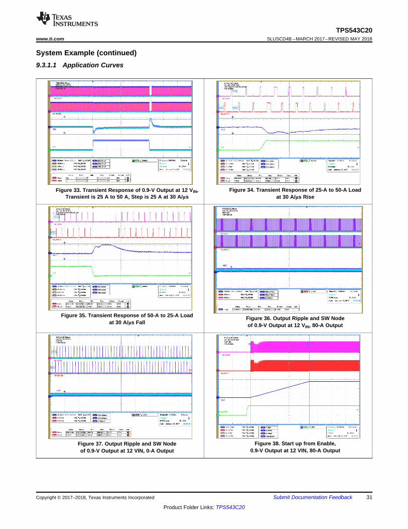
System Example (continued)9.3.1.1 Application Curves
Figure 33. Transient Response of 0.9-V Output at 12 VIN,Transient is 25 A to 50 A, Step is 25 A at 30 A/μs
Figure 34. Transient Response of 25-A to 50-A Loadat 30 A/μs Rise
Figure 35. Transient Response of 50-A to 25-A Loadat 30 A/μs Fall
Figure 36. Output Ripple and SW Nodeof 0.9-V Output at 12 VIN, 80-A Output
Figure 37. Output Ripple and SW Nodeof 0.9-V Output at 12 VIN, 0-A Output
Figure 38. Start up from Enable,0.9-V Output at 12 VIN, 80-A Output

32
TPS543C20SLUSCD4B –MARCH 2017–REVISED MAY 2018 www.ti.com
Product Folder Links: TPS543C20
Submit Documentation Feedback Copyright © 2017–2018, Texas Instruments Incorporated
System Example (continued)
Figure 39. 0.6-V Pre-Bias Start Up From Enable,0.9-V Output at 12 VIN, 0-A Output
Figure 40. Output Voltage Start-up and Shutdown,0.9-V Output at 12 VIN, 5-A Output
Figure 41. Master-Slave 180° Synchronization
10 Power Supply RecommendationsThis device is designed to operate from an input voltage supply between 4 V and 16 V. Ensure the supply is wellregulated. Proper bypassing of input supplies and internal regulators is also critical for noise performance, as isthe quality of the PCB layout and grounding scheme. See the recommendations in Layout.

33
TPS543C20www.ti.com SLUSCD4B –MARCH 2017–REVISED MAY 2018
Product Folder Links: TPS543C20
Submit Documentation FeedbackCopyright © 2017–2018, Texas Instruments Incorporated
11 Layout
11.1 Layout Guidelines• It is absolutely critical that all GND pins, including AGND (pin 29), GND (pin 27), and PGND (pins 13, 14, 15,
16, 17, 18, 19, and 20) are connected directly to the thermal pad underneath the device via traces or plane.The number of thermal vias needed to support 40-A thermal operation should be as many as possible; in theEVM design orderable on the Web, a total of 23 thermal vias are used. The TPS543C20EVM-799 is availablefor purchase at ti.com.
• Place the power components (including input/output capacitors, output inductor, and TPS543C20 device) onone side of the PCB (solder side). At least one or two innner layers/planes should be inserted, connecting topower ground, in order to shield and isolate the small signal traces from noisy power lines.
• Place the VIN decoupling capacitors as close to the PVIN and PGND as possible to minimize the input ACcurrent loop. The high frequency decoupling capacitor (1 nF to 0.1 µF) should be placed next to the PVIN pinand PGND pin as close as the spacing rule allows. This helps surpressing the switch node ringing.
• Place a 10-nF to 100-nF capacitor close to IC from Pin 25 VIN to Pin 27 GND.• Place VDD and BP decoupling capacitors as close to the device pins as possible. Do not use PVIN plane
connection for VDD. VDD needs to be tapped off from PVIN with separate trace connection. Ensure toprovide GND vias for each decoupling capacitor and make the loop as small as possible.
• The PCB trace defined as switch node, which connects the SW pins and up-stream of the output inductorshould be as short and wide as possible. In web orderable EVM design, the SW trace width is 400mil. Useseparate via or trace to connect SW node to snubber and bootstrap capacitor. Do not combine theseconnections.
• All sensitive analog traces and components such as RAMP, RSP, RSN, ILIM, MODE, VSEL and RT shouldbe placed away from any high voltage switch node (itself and others), such as SW and BOOT to avoid noisecoupling. In addition, MODE, VSEL, ILIM, RAMP and RT programming resistors should be placed near thedevice/pins.
• The RSP and RSN pins operate as inputs to a differential remote sense amplifier that operates with very highimpedance. It is essential to route the RSP and RSN pins as a pair of diff-traces in Kelvin-sense fashion.Route them directly to either the load sense points (+ and –) or the output bulk capacitors. The internal circuituses the RSP pin for on-time adjustment. It is critical to tie the RSP pin directly tied to VOUT (load sensepoint) for accurate output voltage result.
• Use caution when routing of the SYNC, VSHARE and ISHARE traces for 2-phase configurations. The SYNCtrace carries a rail-to-rail signal and should be routed away from sensitive analog signals, including theVSHARE, ISHARE, RT, and FB signals. The VSHARE and ISHARE traces should also be kept away fromfast switching voltages or currents formed by the PVIN, AVIN, SW, BOOT, and BP pins.

RBOOT
CBOOT
L1
RSNS±
RSNS+
AGND
VOUT
PGND
PVIN
ENSignal
Bypass for internal regulators BP, VDD.Use multiple vias to reduce parasitic inductance
Optional RC Snubber
Kelvin Connect to IC RSP and RSN pins
Place PVIN bypass capacitors as close as possible to IC, with best high frequency capacitor closest to PVIN/PGND pins
Place best high frequency output
capacitor between sense point
AGND and GND are only connected together on Thermal Pad.
Minimize SW area for least noise. Keep sensitive traces away from SW and BOOT on all layers
Sense point should be directly at the load
For best efficiency, use a heavy weight copper and place these planes on multiple PCB layers
RSP
RSN
RS
P
RS
N
BO
OT
SW
SW
SW
SW
SW
PGND
PGND
PGND
PGND
PGND
PGND
PGND
PGND
ILIM
AG
ND
BP
GN
D
VD
D
PV
IN
PV
IN
PV
IN
PV
IN
PV
IN
EN
PGD
SYNC
VSEL
SS
MODE
RAMP
Thermal Pad
Connect AGND to Thermal Pad
Connect GND to Thermal Pad
RT
Internal AGND Plane to reduce the BP bypass parasitics .
34
TPS543C20SLUSCD4B –MARCH 2017–REVISED MAY 2018 www.ti.com
Product Folder Links: TPS543C20
Submit Documentation Feedback Copyright © 2017–2018, Texas Instruments Incorporated
11.2 Layout Example
Figure 42. Example Layout

Output Current (A)
Am
bien
t Tem
pera
ture
(qC
)
0 5 10 15 20 25 30 35 4030
40
50
60
70
80
90
100
110
D001
Nat Conv100 LFM200 LFM400 LFM
Output Current (A)
Am
bien
t Tem
pera
ture
(qC
)
0 5 10 15 20 25 30 35 4030
40
50
60
70
80
90
100
110
D002
Nat Conv100 LFM200 LFM400 LFM
35
TPS543C20www.ti.com SLUSCD4B –MARCH 2017–REVISED MAY 2018
Product Folder Links: TPS543C20
Submit Documentation FeedbackCopyright © 2017–2018, Texas Instruments Incorporated
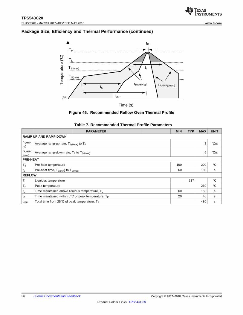
11.3 Package Size, Efficiency and Thermal PerformanceThe TPS543C20 device is available in a 5 mm x 7 mm, QFN package with 40 power and I/O pins. It employs TIproprietary MCM packaging technology with thermal pad. With a properly designed system layout, applicationsachieve optimized safe operating area (SOA) performance. The curves shown in and are based on the orderableevaluation module design.
VIN = 12 V VOUT = 5 V 500 kHz
Figure 43. Safe Operating Area
VIN = 12 V VOUT = 1 V 500 kHz
Figure 44. Safe Operating Area
Figure 45. Thermal Image at 0.9-V Output at 12 VIN, 40-A Output, at 25°C Ambient
Time (s)
Tem
pera
ture
(°C
)
TS(max)
TS(min)
TL
TP
tS
25
rRAMP(up) rRAMP(down)
t25P
tP
tL
36
TPS543C20SLUSCD4B –MARCH 2017–REVISED MAY 2018 www.ti.com
Product Folder Links: TPS543C20
Submit Documentation Feedback Copyright © 2017–2018, Texas Instruments Incorporated
Package Size, Efficiency and Thermal Performance (continued)
Figure 46. Recommended Reflow Oven Thermal Profile
Table 7. Recommended Thermal Profile ParametersPARAMETER MIN TYP MAX UNIT
RAMP UP AND RAMP DOWNrRAMP(up)
Average ramp-up rate, TS(MAX) to TP 3 °C/s
rRAMP(down)
Average ramp-down rate, TP to TS(MAX) 6 °C/s
PRE-HEATTS Pre-heat temperature 150 200 °CtS Pre-heat time, TS(min) to TS(max) 60 180 sREFLOWTL Liquidus temperature 217 °CTP Peak temperature 260 °CtL Time maintained above liquidus temperature, TL 60 150 stP Time maintained within 5°C of peak temperature, TP 20 40 st25P Total time from 25°C of peak temperature, TP 480 s

37
TPS543C20www.ti.com SLUSCD4B –MARCH 2017–REVISED MAY 2018
Product Folder Links: TPS543C20
Submit Documentation FeedbackCopyright © 2017–2018, Texas Instruments Incorporated
12 Device and Documentation Support
12.1 Device Support
12.1.1 Development Support
12.1.1.1 Custom Design With WEBENCH® ToolsClick here to create a custom design using the TPS543C20 device with the WEBENCH® Power Designer.1. Start by entering the input voltage (VIN), output voltage (VOUT), and output current (IOUT) requirements.2. Optimize the design for key parameters such as efficiency, footprint, and cost using the optimizer dial.3. Compare the generated design with other possible solutions from Texas Instruments.
The WEBENCH Power Designer provides a customized schematic along with a list of materials with real-timepricing and component availability.
In most cases, these actions are available:• Run electrical simulations to see important waveforms and circuit performance• Run thermal simulations to understand board thermal performance• Export customized schematic and layout into popular CAD formats• Print PDF reports for the design, and share the design with colleagues
Get more information about WEBENCH tools at www.ti.com/WEBENCH.
12.1.2 Documentation Support
12.1.2.1 Related DocumentationFor related documentation see the following:
TPS543B20 40-A Single Phase Synchronous Step-Down Converter
12.2 Receiving Notification of Documentation UpdatesTo receive notification of documentation updates, navigate to the device product folder on ti.com. In the upperright corner, click on Alert me to register and receive a weekly digest of any product information that haschanged. For change details, review the revision history included in any revised document.
12.3 Community ResourcesThe following links connect to TI community resources. Linked contents are provided "AS IS" by the respectivecontributors. They do not constitute TI specifications and do not necessarily reflect TI's views; see TI's Terms ofUse.
TI E2E™ Online Community TI's Engineer-to-Engineer (E2E) Community. Created to foster collaborationamong engineers. At e2e.ti.com, you can ask questions, share knowledge, explore ideas and helpsolve problems with fellow engineers.
Design Support TI's Design Support Quickly find helpful E2E forums along with design support tools andcontact information for technical support.
12.4 TrademarksNexFET, PowerStack, E2E are trademarks of Texas Instruments.WEBENCH is a registered trademark of Texas Instruments.All other trademarks are the property of their respective owners.
12.5 Electrostatic Discharge CautionThese devices have limited built-in ESD protection. The leads should be shorted together or the device placed in conductive foamduring storage or handling to prevent electrostatic damage to the MOS gates.

38
TPS543C20SLUSCD4B –MARCH 2017–REVISED MAY 2018 www.ti.com
Product Folder Links: TPS543C20
Submit Documentation Feedback Copyright © 2017–2018, Texas Instruments Incorporated
12.6 GlossarySLYZ022 — TI Glossary.
This glossary lists and explains terms, acronyms, and definitions.
13 Mechanical, Packaging, and Orderable InformationThe following pages include mechanical, packaging, and orderable information. This information is the mostcurrent data available for the designated devices. This data is subject to change without notice and revision ofthis document. For browser-based versions of this data sheet, refer to the left-hand navigation.

PACKAGE OPTION ADDENDUM
www.ti.com 10-Dec-2020
Addendum-Page 1
PACKAGING INFORMATION
Orderable Device Status(1)
Package Type PackageDrawing
Pins PackageQty
Eco Plan(2)
Lead finish/Ball material
(6)
MSL Peak Temp(3)
Op Temp (°C) Device Marking(4/5)
Samples
TPS543C20RVFR ACTIVE LQFN-CLIP RVF 40 2500 RoHS-Exempt& Green
NIPDAU Level-2-260C-1 YEAR -40 to 125 TPS543C20
TPS543C20RVFT ACTIVE LQFN-CLIP RVF 40 250 RoHS-Exempt& Green
NIPDAU Level-2-260C-1 YEAR -40 to 125 TPS543C20
(1) The marketing status values are defined as follows:ACTIVE: Product device recommended for new designs.LIFEBUY: TI has announced that the device will be discontinued, and a lifetime-buy period is in effect.NRND: Not recommended for new designs. Device is in production to support existing customers, but TI does not recommend using this part in a new design.PREVIEW: Device has been announced but is not in production. Samples may or may not be available.OBSOLETE: TI has discontinued the production of the device.
(2) RoHS: TI defines "RoHS" to mean semiconductor products that are compliant with the current EU RoHS requirements for all 10 RoHS substances, including the requirement that RoHS substancedo not exceed 0.1% by weight in homogeneous materials. Where designed to be soldered at high temperatures, "RoHS" products are suitable for use in specified lead-free processes. TI mayreference these types of products as "Pb-Free".RoHS Exempt: TI defines "RoHS Exempt" to mean products that contain lead but are compliant with EU RoHS pursuant to a specific EU RoHS exemption.Green: TI defines "Green" to mean the content of Chlorine (Cl) and Bromine (Br) based flame retardants meet JS709B low halogen requirements of <=1000ppm threshold. Antimony trioxide basedflame retardants must also meet the <=1000ppm threshold requirement.
(3) MSL, Peak Temp. - The Moisture Sensitivity Level rating according to the JEDEC industry standard classifications, and peak solder temperature.
(4) There may be additional marking, which relates to the logo, the lot trace code information, or the environmental category on the device.
(5) Multiple Device Markings will be inside parentheses. Only one Device Marking contained in parentheses and separated by a "~" will appear on a device. If a line is indented then it is a continuationof the previous line and the two combined represent the entire Device Marking for that device.
(6) Lead finish/Ball material - Orderable Devices may have multiple material finish options. Finish options are separated by a vertical ruled line. Lead finish/Ball material values may wrap to twolines if the finish value exceeds the maximum column width.
Important Information and Disclaimer:The information provided on this page represents TI's knowledge and belief as of the date that it is provided. TI bases its knowledge and belief on informationprovided by third parties, and makes no representation or warranty as to the accuracy of such information. Efforts are underway to better integrate information from third parties. TI has taken andcontinues to take reasonable steps to provide representative and accurate information but may not have conducted destructive testing or chemical analysis on incoming materials and chemicals.TI and TI suppliers consider certain information to be proprietary, and thus CAS numbers and other limited information may not be available for release.
In no event shall TI's liability arising out of such information exceed the total purchase price of the TI part(s) at issue in this document sold by TI to Customer on an annual basis.

PACKAGE OPTION ADDENDUM
www.ti.com 10-Dec-2020
Addendum-Page 2

TAPE AND REEL INFORMATION
*All dimensions are nominal
Device PackageType
PackageDrawing
Pins SPQ ReelDiameter
(mm)
ReelWidth
W1 (mm)
A0(mm)
B0(mm)
K0(mm)
P1(mm)
W(mm)
Pin1Quadrant
TPS543C20RVFR LQFN-CLIP
RVF 40 2500 330.0 16.4 5.35 7.35 1.7 8.0 16.0 Q1
TPS543C20RVFT LQFN-CLIP
RVF 40 250 180.0 16.4 5.35 7.35 1.7 8.0 16.0 Q1
PACKAGE MATERIALS INFORMATION
www.ti.com 15-Feb-2019
Pack Materials-Page 1

*All dimensions are nominal
Device Package Type Package Drawing Pins SPQ Length (mm) Width (mm) Height (mm)
TPS543C20RVFR LQFN-CLIP RVF 40 2500 367.0 367.0 38.0
TPS543C20RVFT LQFN-CLIP RVF 40 250 210.0 185.0 35.0
PACKAGE MATERIALS INFORMATION
www.ti.com 15-Feb-2019
Pack Materials-Page 2
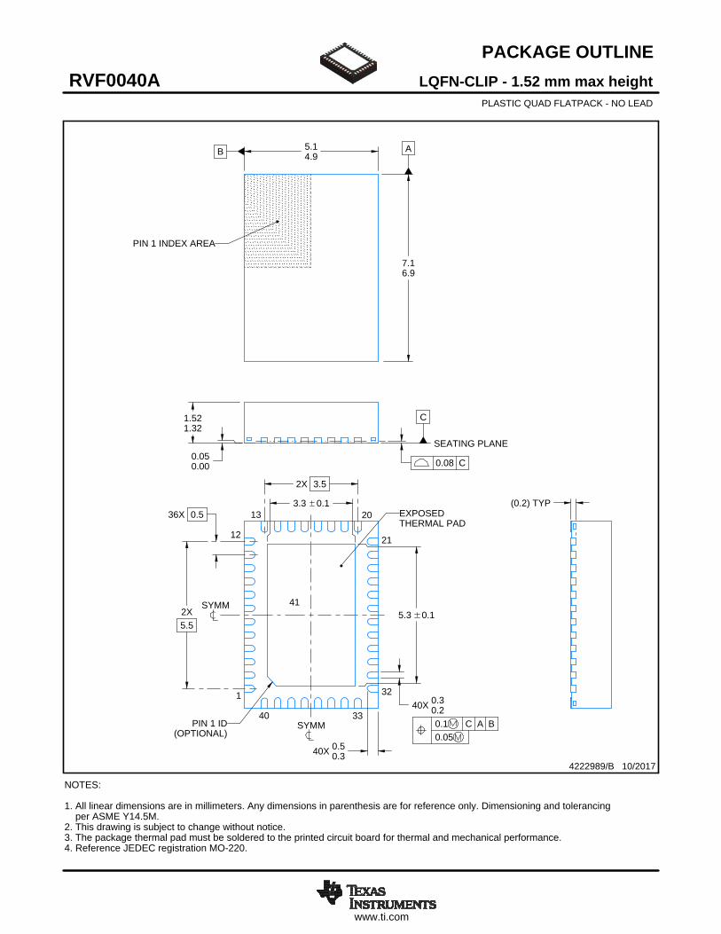
www.ti.com
PACKAGE OUTLINE
C
40X 0.30.2
3.3 0.1
40X 0.50.3
1.521.32
(0.2) TYP
0.050.00
36X 0.5
2X5.5
2X 3.5
5.3 0.1
B 5.14.9
A
7.16.9
LQFN-CLIP - 1.52 mm max heightRVF0040APLASTIC QUAD FLATPACK - NO LEAD
4222989/B 10/2017
PIN 1 INDEX AREA
0.08 C
SEATING PLANE
1
12 21
32
13 20
40 33
(OPTIONAL)PIN 1 ID 0.1 C A B
0.05
EXPOSEDTHERMAL PAD
SYMM
SYMM
41
NOTES: 1. All linear dimensions are in millimeters. Any dimensions in parenthesis are for reference only. Dimensioning and tolerancing per ASME Y14.5M. 2. This drawing is subject to change without notice. 3. The package thermal pad must be soldered to the printed circuit board for thermal and mechanical performance.4. Reference JEDEC registration MO-220.
SCALE 2.000

www.ti.com
EXAMPLE BOARD LAYOUT
0.07 MINALL AROUND
0.07 MAXALL AROUND
40X (0.25)
40X (0.6)
( 0.2) TYPVIA
36X (0.5)
(6.8)
(4.8)
6X(1.28)
(3.3)
(R0.05) TYP
(5.3)
6X (1.4)
2X(1.12)
LQFN-CLIP - 1.52 mm max heightRVF0040APLASTIC QUAD FLATPACK - NO LEAD
4222989/B 10/2017
SYMM
1
12
13 20
21
32
3340
SYMM
LAND PATTERN EXAMPLESCALE:12X
41
NOTES: (continued) 5. This package is designed to be soldered to a thermal pad on the board. For more information, see Texas Instruments literature number SLUA271 (www.ti.com/lit/slua271).
SOLDER MASKOPENING
METAL UNDERSOLDER MASK
SOLDER MASKDEFINED
METAL
SOLDER MASKOPENING
SOLDER MASK DETAILS
NON SOLDER MASKDEFINED
(PREFERRED)

www.ti.com
EXAMPLE STENCIL DESIGN
40X (0.6)
40X (0.25)
36X (0.5)
(4.8)
(6.8)
8X (1.43)
(1.28)TYP
(0.815) TYP
(R0.05) TYP
(0.64)TYP
8X(1.08)
LQFN-CLIP - 1.52 mm max heightRVF0040APLASTIC QUAD FLATPACK - NO LEAD
4222989/B 10/2017
NOTES: (continued) 6. Laser cutting apertures with trapezoidal walls and rounded corners may offer better paste release. IPC-7525 may have alternate design recommendations.
SYMM
METALTYP
SOLDER PASTE EXAMPLEBASED ON 0.125 mm THICK STENCIL
EXPOSED PAD
71% PRINTED SOLDER COVERAGE BY AREASCALE:18X
SYMM
1
12
13 20
21
32
3340
41

IMPORTANT NOTICE AND DISCLAIMER
TI PROVIDES TECHNICAL AND RELIABILITY DATA (INCLUDING DATASHEETS), DESIGN RESOURCES (INCLUDING REFERENCE DESIGNS), APPLICATION OR OTHER DESIGN ADVICE, WEB TOOLS, SAFETY INFORMATION, AND OTHER RESOURCES “AS IS” AND WITH ALL FAULTS, AND DISCLAIMS ALL WARRANTIES, EXPRESS AND IMPLIED, INCLUDING WITHOUT LIMITATION ANY IMPLIED WARRANTIES OF MERCHANTABILITY, FITNESS FOR A PARTICULAR PURPOSE OR NON-INFRINGEMENT OF THIRD PARTY INTELLECTUAL PROPERTY RIGHTS.These resources are intended for skilled developers designing with TI products. You are solely responsible for (1) selecting the appropriate TI products for your application, (2) designing, validating and testing your application, and (3) ensuring your application meets applicable standards, and any other safety, security, or other requirements. These resources are subject to change without notice. TI grants you permission to use these resources only for development of an application that uses the TI products described in the resource. Other reproduction and display of these resources is prohibited. No license is granted to any other TI intellectual property right or to any third party intellectual property right. TI disclaims responsibility for, and you will fully indemnify TI and its representatives against, any claims, damages, costs, losses, and liabilities arising out of your use of these resources.TI’s products are provided subject to TI’s Terms of Sale (www.ti.com/legal/termsofsale.html) or other applicable terms available either on ti.com or provided in conjunction with such TI products. TI’s provision of these resources does not expand or otherwise alter TI’s applicable warranties or warranty disclaimers for TI products.
Mailing Address: Texas Instruments, Post Office Box 655303, Dallas, Texas 75265Copyright © 2020, Texas Instruments Incorporated