tps28225 high-frequency 4-a sink synchronous … · 3 3 boot 2 ugate phase lgate gnd 1 8 5 4 6 vdd...
TRANSCRIPT

3
3
2BOOT
UGATE
PHASE
LGATE
GND
1
8
5
4
6 VDD
ENBL7
PWM3
OUT
FB
3GND
3
TPS28225
VDD (4.5 V to 8 V) VIN (3 V to 32 V − VDD)
VOUTVCC
TPS40200
Product
Folder
Sample &Buy
Technical
Documents
Tools &
Software
Support &Community
ReferenceDesign
TPS28225SLUS710D –MAY 2006–REVISED SEPTEMBER 2015
TPS28225 High-Frequency 4-A Sink Synchronous MOSFET Drivers1 Features 2 Applications1• Drives Two N-Channel MOSFETs with 14-ns • Multi-Phase DC-to-DC Converters with Analog or
Adaptive Dead Time Digital Control• Wide Gate Drive Voltage: 4.5 V Up to 8.8 V With • Desktop and Server VRMs and EVRDs
Best Efficiency at 7 V to 8 V • Portable and Notebook Regulators• Wide Power System Train Input Voltage: 3 V Up • Synchronous Rectification for Isolated Power
to 27 V Supplies• Wide Input PWM Signals: 2.0 V up to 13.2-V
3 DescriptionAmplitudeThe TPS28225 is a high-speed driver for N-channel• Capable to Drive MOSFETs with ≥40-A Currentcomplimentary driven power MOSFETs with adaptiveper Phasedead-time control. This driver is optimized for use in• High Frequency Operation: 14-ns Propagation variety of high-current one and multi-phase DC-to-DCDelay and 10-ns Rise/Fall Time Allow FSW – 2 converters. The TPS28225 is a solution that provides
MHz high efficiency, small size and low EMI emissions.• Capable to Propagate <30-ns Input PWM Pulses The efficiency is achieved by up to 8.8-V gate drive• Low-Side Driver Sink On-Resistance (0.4 Ω) voltage, 14-ns adaptive dead-time control, 14-ns
Prevents dV/dT Related Shoot-Through Current propagation delays and high-current 2-A source and4-A sink drive capability. The 0.4-Ω impedance for• 3-State PWM Input for Power Stage Shutdownthe lower gate driver holds the gate of power• Space Saving Enable (Input) and Power GoodMOSFET below its threshold and ensures no shoot-(Output) Signals on Same Pin through current at high dV/dt phase node transitions.
• Thermal Shutdown The bootstrap capacitor charged by an internal diodeallows use of N-channel MOSFETs in a half-bridge• UVLO Protectionconfiguration.• Internal Bootstrap Diode
• Economical SOIC-8 and Thermally Enhanced 3- Device Information(1)mm x 3-mm DFN-8 Packages PART NUMBER PACKAGE BODY SIZE (NOM)
• High Performance Replacement for Popular 3- SOIC (8) 4.90 mm × 3.91 mmTPS28225State Input Drivers VSON (8) 3.00 mm x 3.00 mm
(1) For all available packages, see the orderable addendum atthe end of the data sheet.
Simplified Schematic
1
An IMPORTANT NOTICE at the end of this data sheet addresses availability, warranty, changes, use in safety-critical applications,intellectual property matters and other important disclaimers. PRODUCTION DATA.

TPS28225SLUS710D –MAY 2006–REVISED SEPTEMBER 2015 www.ti.com
Table of Contents7.4 Device Functional Modes........................................ 161 Features .................................................................. 1
8 Application and Implementation ........................ 162 Applications ........................................................... 18.1 Application Information............................................ 163 Description ............................................................. 18.2 Typical Application ................................................. 174 Revision History..................................................... 28.3 System Examples ................................................... 245 Pin Configuration and Functions ......................... 3
9 Power Supply Recommendations ...................... 266 Specifications......................................................... 410 Layout................................................................... 266.1 Absolute Maximum Ratings ...................................... 4
10.1 Layout Guidelines ................................................. 266.2 ESD Ratings ............................................................ 410.2 Layout Example .................................................... 276.3 Recommended Operating Conditions....................... 4
11 Device and Documentation Support ................. 286.4 Thermal Information .................................................. 511.1 Device Support .................................................... 286.5 Electrical Characteristics .......................................... 511.2 Documentation Support ....................................... 286.6 Switching Characteristics .......................................... 611.3 Community Resources.......................................... 286.7 Typical Characteristics .............................................. 711.4 Trademarks ........................................................... 287 Detailed Description ............................................ 1011.5 Electrostatic Discharge Caution............................ 287.1 Overview ................................................................. 1011.6 Glossary ................................................................ 287.2 Functional Block Diagram ....................................... 10
12 Mechanical, Packaging, and Orderable7.3 Feature Description................................................. 11Information ........................................................... 28
4 Revision HistoryNOTE: Page numbers for previous revisions may differ from page numbers in the current version.
Changes from Revision C (April 2010) to Revision D Page
• Added Pin Configuration and Functions section, Handling Rating table, Feature Description section, DeviceFunctional Modes, Application and Implementation section, Power Supply Recommendations section, Layoutsection, Device and Documentation Support section, and Mechanical, Packaging, and Orderable Informationsection ................................................................................................................................................................................... 1
• Deleted the TPS28226 device. .............................................................................................................................................. 1
Changes from Revision B (July 2007) to Revision C Page
• Changed FUNCTIONAL BLOCK DIAGRAM .......................................................................................................................... 3
2 Submit Documentation Feedback Copyright © 2006–2015, Texas Instruments Incorporated
Product Folder Links: TPS28225

5
3
7
6
81
2BOOT
PWM VDD
EN/PG
GND
PHASE
4
ExposedThermalDie Pad
LGATE
UGATE
1
2
3
4
8
7
6
5
UGATE
BOOT
PWM
GND
PHASE
EN/PG
VDD
LGATE
TPS28225www.ti.com SLUS710D –MAY 2006–REVISED SEPTEMBER 2015
5 Pin Configuration and Functions
D Package8-Pin SOICTop View
DRB Package8-Pin VSON
Top View
Pin FunctionsPIN
NO. I/O DESCRIPTIONNAME
SOIC VSONFloating bootstrap supply pin for the upper gate drive. Connect the bootstrap
BOOT 2 2 I/O capacitor between this pin and the Phase pin. The bootstrap capacitorprovides the charge to turn on the upper MOSFET.Enable/power good input/output pin with 1-MΩ impedance. Connect this pinto High to enable and Low to disable the device. When disabled, the deviceEN/PG 7 7 I/O draws less than 350-μA bias current. If the VDD is below UVLO threshold orover temperature shutdown occurs, this pin is internally pulled low.
GND 4 4 – Ground pin. All signals are referenced to this node.Lower gate drive sink and source output. Connect to the gate of the low-sideLGATE 5 5 O power N-Channel MOSFET.Connect this pin to the source of the upper MOSFET and the drain of thePHASE 8 8 I lower MOSFET. This pin provides a return path for the upper gate driver.The PWM signal is the control input for the driver. The PWM signal can enterthree distinct states during operation, see the 3-state PWM Input sectionPWM 3 3 I under DETAILED DESCRIPTION for further details. Connect this pin to thePWM output of the controller.
Exposed dieThermal pad – Connect directly to the GND for better thermal performance and EMI.padUpper gate drive sink/source output. Connect to gate of high-side power N-UGATE 1 1 O Channel MOSFET.Connect this pin to a 5-V bias supply. Place a high quality bypass capacitorVDD 6 6 I from this pin to GND.
Copyright © 2006–2015, Texas Instruments Incorporated Submit Documentation Feedback 3
Product Folder Links: TPS28225
TPS28225SLUS710D –MAY 2006–REVISED SEPTEMBER 2015 www.ti.com
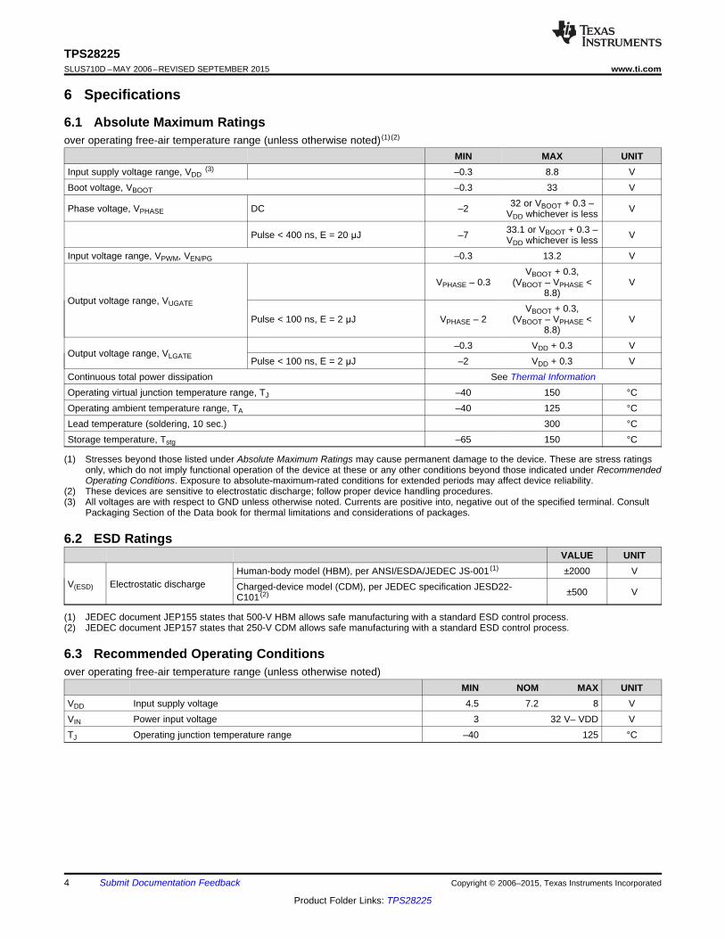
6 Specifications
6.1 Absolute Maximum Ratingsover operating free-air temperature range (unless otherwise noted) (1) (2)
MIN MAX UNITInput supply voltage range, VDD
(3) –0.3 8.8 VBoot voltage, VBOOT –0.3 33 V
32 or VBOOT + 0.3 –Phase voltage, VPHASE DC –2 VVDD whichever is less33.1 or VBOOT + 0.3 –Pulse < 400 ns, E = 20 μJ –7 VVDD whichever is less
Input voltage range, VPWM, VEN/PG –0.3 13.2 VVBOOT + 0.3,
VPHASE – 0.3 (VBOOT – VPHASE < V8.8)
Output voltage range, VUGATE VBOOT + 0.3,Pulse < 100 ns, E = 2 μJ VPHASE – 2 (VBOOT – VPHASE < V
8.8)–0.3 VDD + 0.3 V
Output voltage range, VLGATE Pulse < 100 ns, E = 2 μJ –2 VDD + 0.3 VContinuous total power dissipation See Thermal InformationOperating virtual junction temperature range, TJ –40 150 °COperating ambient temperature range, TA –40 125 °CLead temperature (soldering, 10 sec.) 300 °CStorage temperature, Tstg –65 150 °C
(1) Stresses beyond those listed under Absolute Maximum Ratings may cause permanent damage to the device. These are stress ratingsonly, which do not imply functional operation of the device at these or any other conditions beyond those indicated under RecommendedOperating Conditions. Exposure to absolute-maximum-rated conditions for extended periods may affect device reliability.
(2) These devices are sensitive to electrostatic discharge; follow proper device handling procedures.(3) All voltages are with respect to GND unless otherwise noted. Currents are positive into, negative out of the specified terminal. Consult
Packaging Section of the Data book for thermal limitations and considerations of packages.
6.2 ESD RatingsVALUE UNIT
Human-body model (HBM), per ANSI/ESDA/JEDEC JS-001 (1) ±2000 VV(ESD) Electrostatic discharge Charged-device model (CDM), per JEDEC specification JESD22- ±500 VC101 (2)
(1) JEDEC document JEP155 states that 500-V HBM allows safe manufacturing with a standard ESD control process.(2) JEDEC document JEP157 states that 250-V CDM allows safe manufacturing with a standard ESD control process.
6.3 Recommended Operating Conditionsover operating free-air temperature range (unless otherwise noted)
MIN NOM MAX UNITVDD Input supply voltage 4.5 7.2 8 VVIN Power input voltage 3 32 V– VDD VTJ Operating junction temperature range –40 125 °C
4 Submit Documentation Feedback Copyright © 2006–2015, Texas Instruments Incorporated
Product Folder Links: TPS28225

TPS28225www.ti.com SLUS710D –MAY 2006–REVISED SEPTEMBER 2015
6.4 Thermal InformationTPS28225
THERMAL METRIC VSON (DRB) SOIC (D) UNIT8 PINS 8 PINS
RθJA Junction-to-ambient thermal resistance 50.2 123.2 °C/WRθJC(top) Junction-to-case (top) thermal resistance 57.5 77.0 °C/WRθJB Junction-to-board thermal resistance 25.9 63.5 °C/WψJT Junction-to-top characterization parameter 1.5 27.7 °C/WψJB Junction-to-board characterization parameter 26.0 63.0 °C/WRθJC(bot) Junction-to-case (bottom) thermal resistance 9.5 N/A °C/W
6.5 Electrical Characteristics (1)
VDD = 7.2 V, EN/PG pulled up to VDD by 100-kΩ resistor, TA = TJ = –40°C to 125°C (unless otherwise noted)PARAMETER TEST CONDITIONS MIN TYP MAX UNIT
UNDER VOLTAGE LOCKOUTRising threshold VPWM = 0 V 3.2 3.5 3.8 VFalling threshold VPWM = 0 V 2.7 3.0 VHysteresis 0.5 V
BIAS CURRENTSIDD(off) Bias supply current VEN/PG = low, PWM pin floating 350 μAIDD Bias supply current VEN/PG = high, PWM pin floating 500 μAINPUT (PWM)
VPWM = 5 V 185 μAIPWM Input current
VPWM = 0 V –200 μAPWM 3-state rising threshold (2) 1.0 VPWM 3-state falling threshold VPWM PEAK = 5 V 3.4 3.8 4.0 V
tHLD_R 3-state shutdown Hold-off time 250 nsPWM minimum pulse to force UGATETMIN CL = 3 nF at UGATE , VPWM = 5 V 30 nspulse
ENABLE/POWER GOOD (EN/PG)Enable high rising threshold PG FET OFF 1.7 2.1 VEnable low falling threshold PG FET OFF 0.8 1.0 VHysteresis 0.35 0.70 VPower good output VDD = 2.5 V 0.2 V
UPPER GATE DRIVER OUTPUT (UGATE)Source resistance 500 mA source current 1.0 2.0 ΩSource current (2) VUGATE-PHASE = 2.5 V 2.0 A
tRU Rise time CL = 3 nF 10 nsSink resistance 500 mA sink current 1.0 2.0 ΩSink current (2) VUGATE-PHASE = 2.5 V 2.0 A
tFU Fall time CL = 3 nF 10 ns
(1) Typical values for TA = 25°C(2) Not production tested.
Copyright © 2006–2015, Texas Instruments Incorporated Submit Documentation Feedback 5
Product Folder Links: TPS28225

Normal switching
PWM
LGATE
UGATE
3-State
window
90%
10%
tDLL
50%
tFL
50%
tPWM_MIN
tDTU
90%
10%
tRU
90%
10%tDLU
tFU
tDTL
90%
10%
tRL
tHLD_R
90%
10%
90%
90%
tHLD_F
Enter into 3-State
at PWM riseExit 3-State
Enter into 3-State
at PWM fall
UGATE exits 3-State after PWM
goes Low and then High
TPS28225SLUS710D –MAY 2006–REVISED SEPTEMBER 2015 www.ti.com
Electrical Characteristics(1) (continued)VDD = 7.2 V, EN/PG pulled up to VDD by 100-kΩ resistor, TA = TJ = –40°C to 125°C (unless otherwise noted)
PARAMETER TEST CONDITIONS MIN TYP MAX UNITLOWER GATE DRIVER OUTPUT (LGATE)
Source resistance 500 mA source current 1.0 2.0 ΩSource current (2) VLGATE = 2.5 V 2.0 A
tRL Rise time (2) CL = 3 nF 10 nsSink resistance 500 mA sink current 0.4 1.0 ΩSink current (2) VLGATE = 2.5 V 4.0 AFall time (2) CL = 3 nF 5 ns
BOOTSTRAP DIODEVF Forward voltage Forward bias current 100 mA 1.0 VTHERMAL SHUTDOWN
Rising threshold (2) 150 160 170 °CFalling threshold (2) 130 140 150 °CHysteresis 20 °C
6.6 Switching Characteristicsover operating free-air temperature range (unless otherwise noted)
PARAMETER TEST CONDITIONS MIN TYP MAX UNITSWITCHING TIMEtDLU UGATE turn-off propagation Delay CL = 3 nF 14 nstDLL LGATE turn-off propagation Delay CL = 3 nF 14 ns
Dead time LGATE turn off totDTU CL = 3 nF 14 nsUGATE turn onDead time UGATE turn off totDTL CL = 3 nF 14 nsLGATE turn on
Figure 1. TPS28225 Timing Diagram
6 Submit Documentation Feedback Copyright © 2006–2015, Texas Instruments Incorporated
Product Folder Links: TPS28225

0
-40 12525
0.75
1.25
2.00
0.25
0.50
1.00
1.50
1.75
RO
UT-
Ou
tpu
t Im
pe
da
nce
- :
TJ - Temperature - °C
RSINK
RSOURCE
0
RO
UT-
Ou
tpu
t Im
pe
da
nce
- :
-40 125
TJ - Temperature - °C
25
0.75
1.25
2.00
0.25
0.50
1.00
1.50
1.75
RSINK
RSOURCE
EN
/PG
- E
na
ble
/Po
we
r G
oo
d -
V
-40 125
TJ - Temperature - °C
25
Falling
Rising
0.00
0.75
1.25
2.00
0.25
0.50
1.00
1.50
1.75
0.0
PW
M -
PW
M 3
-Sta
te T
hre
sho
ld -
V
-40 125
TJ - Temperature - °C
25
Falling
Rising
2.0
3.0
5.0
0.5
1.0
2.5
2.5
4.5
1.5
4.0
2.00
3.50
4.50
6.00
2.50
3.00
4.00
5.00
5.50
UV
LO -
Un
de
r V
olt
ag
e L
ock
ou
t -
V
-40 125
TJ - Temperature - °C
25
6.50
8.00
7.00
7.50
TPS28225 Falling
TPS28225 Rising
300
360
380
440
320
340
400
420
I DD
(off
) t B
ias
Su
pp
ly -
PA
-40 125
TJ - Temperature - °C
25
460
500
480
TPS28225www.ti.com SLUS710D –MAY 2006–REVISED SEPTEMBER 2015
6.7 Typical Characteristics
VEN/PG = Low PWM Input Floating VDD = 7.2 V
Figure 2. Bias Supply Current vs Temperature Figure 3. Undervoltage Lockout Threshold vs Temperature
VDD = 7.2 VVDD = 7.2 VFigure 5. PWM 3-State Thresholds, (5-V Input Pulses) vsFigure 4. Enable/Power Good Threshold vs Temperature Temperature
VDD = 7.2 VVDD = 7.2 V
Figure 7. LGATE DC Output Impedance vs TemperatureFigure 6. UGATE DC Output Impedance vs Temperature
Copyright © 2006–2015, Texas Instruments Incorporated Submit Documentation Feedback 7
Product Folder Links: TPS28225

0
5
25
30
10
15
20
TM
IN -
Min
imu
m S
ho
rt P
uls
e -
ns
-40 125
TJ - Temperature - °C
25
0.5
0.8
1.0
1.3
0.6
0.7
0.9
1.1
1.2
VF -
Fo
rww
ard
Vo
lta
ge
- V
-40 125
TJ - Temperature - °C
25
0
20
25
30
5
10
15
t DLU
an
d t
DLL
- U
GA
TE a
nd
LG
AT
E -
ns
-40 125
TJ - Temperature - °C
25
LGATE
UGATE
-40 125
TJ - Temperature - °C
25
0.0
12.5
17.5
20.0
2.5
7.5
10.0
t DT
U a
nd
tD
TL -
UG
AT
E a
nd
L G
AT
E -
ns
LGATE
UGATE
5.0
15.0
6
8
11
13
15
7
9
10
12
14
t RU a
nd
tF
U -
Ris
e a
nd
Fa
ll T
ime
- n
s
-40 125
TJ - Temperature - °C
25
Fall
Rise
-40 125
TJ - Temperature - °C
25
4
6
10
12
14
5
7
9
11
13
t RL
an
d t
FL
- R
ise
an
d F
all
Tim
e -
ns
8
Fall
Rise
TPS28225SLUS710D –MAY 2006–REVISED SEPTEMBER 2015 www.ti.com
Typical Characteristics (continued)
VDD = 7.2 V CLOAD = 3 nF VDD = 7.2 V CLOAD = 3 nF
Figure 8. UGATE Rise and Fall Time vs Temperature Figure 9. LGATE Rise and Fall Time vs Temperature
VDD = 7.2 V CLOAD = 3 nFVDD = 7.2 V CLOAD = 3 nF
Figure 11. UGATE and LGATE (Dead Time) vs TempertureFigure 10. UGATE and LGATE (Turning OFF PropagationDelays) vs Temperture
VDD = 7.2 V CLOAD = 3 nF VDD = 7.2 V IF = 100 mA
Figure 12. UGATE Minimum Short Pulse vs Temperature Figure 13. Bootstrap Diode Forward Voltage vs Temperature
8 Submit Documentation Feedback Copyright © 2006–2015, Texas Instruments Incorporated
Product Folder Links: TPS28225

PWM 30ns
UGATE
LGATE
Vo
ltag
e ±
5 V
/div
t ± Time ± 20 ns/div
VDD = 7.2 V, CL = 3 nF, TJ = 25oC
PWM ± 2 V/div
UGATE ± 10 V/div
LGATE ± 10 V/div
Vo
ltag
e
t ± Time ± 5 és/div
3-St Trigger, High = 3-St
PWM
UGATE
LGATE
Vo
ltag
e ±
5 V
/div
t ± Time ± 10 ns/div
VDD = 7.2 V, CL = 3 nF, TJ = 25oC
PWM
UGATE
LGATE
Vo
ltag
e ±
5 V
/div
t ± Time ± 10 ns/div
VDD = 7.2 V, CL = 3 nF, TJ = 25oC
FSW - Switching Frequency - kHz
0
15
5
10
I DD -
Bia
s S
up
ply
Cu
rre
nt
- m
A
100 300 500 700 1500 1700900 1100 19001300
0
200
1000
1200
400
600
800
PD
ISS -
Dis
sip
ate
d P
ow
er
- m
W
100 300 500 700 1500 1700
FSW - Switching Frequency - kHz
900 1100 19001300
UG = 25 nC,
LG = 50 nC
UG = 50 nC, LG = 50 nC
UG = 25 nC,
LG = 100 nC
TPS28225www.ti.com SLUS710D –MAY 2006–REVISED SEPTEMBER 2015
Typical Characteristics (continued)
Different Load VDD = 7.2 V TJ = 25°CNo Load VDD = 7.2 V TJ = 25°CCharge
Figure 14. Bias Supply Current vs Switching FrequencyFigure 15. Driver Dissipated Power vs Switching Frequency
Figure 16. PWM Input Rising Switching Waveforms Figure 17. PWM Input Falling Switching Waveforms
Figure 19. Normal and 3-State Operation Enter/ExitFigure 18. Minimum UGATE Pulse Switching WaveformsConditions
Copyright © 2006–2015, Texas Instruments Incorporated Submit Documentation Feedback 9
Product Folder Links: TPS28225

6
13K
2VDD
EN/PG
BOOT
UGATE
PHASE
LGATE
GND
7
1
8
5
4
VDD27K
3-STATE
INPUT
CIRCUITPWM 3
SHOOT-
THROUGH
PROTECTION
THERMAL
SD
HLD-OFF
TIME
UVLO
TPS28225SLUS710D –MAY 2006–REVISED SEPTEMBER 2015 www.ti.com
7 Detailed Description
7.1 OverviewThe TPS28225 features a 3-state PWM input compatible with all multi-phase controllers employing 3-state outputfeature. As long as the input stays within 3-state window for the 250-ns hold-off time, the driver switches bothoutputs low. This shutdown mode prevents a load from the reversed- output-voltage.
The other features include undervoltage lockout, thermal shutdown and two-way enable/power good signal.Systems without 3-state featured controllers can use enable/power good input/output to hold both outputs lowduring shutting down.
The TPS28225 is offered in an economical SOIC-8 and thermally enhanced low-size Dual Flat No-Lead (DFN-8)packages. The driver is specified in the extended temperature range of –40°C to 125°C with the absolutemaximum junction temperature 150°C.
7.2 Functional Block Diagram
For the TPS28225DRB the thermal PAD on the bottom side of package must be soldered and connected to the GNDpin and to the GND plane of the PCB in the shortest possible way.
10 Submit Documentation Feedback Copyright © 2006–2015, Texas Instruments Incorporated
Product Folder Links: TPS28225

TPS28225www.ti.com SLUS710D –MAY 2006–REVISED SEPTEMBER 2015
7.3 Feature Description
7.3.1 Undervoltage Lockout (UVLO)The TPS28225 incorporates an under voltage lockout circuit that keeps the driver disabled and external powerFETs in an OFF state when the input supply voltage VDD is insufficient to drive external power FETsreliably.During power up, both gate drive outputs remain low until voltage VDD reaches UVLO threshold, typically3.5 V . Once the UVLO threshold is reached, the condition of the gate drive outputs is defined by the input PWMand EN/PG signals. During power down the UVLO threshold is set lower, typically 3.0 V. The 0.5 V for theTPS28225 hysteresis is selected to prevent the driver from turning ON and OFF while the input voltage crossesUVLO thresholds, especially with low slew rate. The TPS28225 has the ability to send a signal back to thesystem controller that the input supply voltage VDD is insufficient by internally pulling down the EN/PG pin. TheTPS28225 releases EN/PG pin immediately after the VDD has risen above the UVLO threshold.
7.3.2 Output Active LowThe output active-low circuit effectively keeps the gate outputs low even if the driver is not powered up. Thisprevents open-gate conditions on the external power FETs and accidental turn on when the main power-stagesupply voltage is applied before the driver is powered up. For the simplicity, the output active low circuit is shownin a block diagram as the resistor connected between LGATE and GND pins with another one connectedbetween UGATE and PHASE pins.
Copyright © 2006–2015, Texas Instruments Incorporated Submit Documentation Feedback 11
Product Folder Links: TPS28225

Thermal SD
UVLO
7EN/PG
Driver TPS28225
1 k:
VCC
6
VDD = 4.5 V to 8 V
820 k:
RDS(on) = 1 k:
2 V Rise 1 V Fall
1 M
System Controller
TPS28225SLUS710D –MAY 2006–REVISED SEPTEMBER 2015 www.ti.com
Feature Description (continued)7.3.3 Enable/Power GoodThe Enable/Power Good circuit allows the TPS28225 to follow the PWM input signal when the voltage at EN/PGpin is above 2.1 V maximum. This circuit has a unique two-way communication capability. This is illustrated byFigure 20.
Figure 20. Enable/Power Good Circuit
The EN/PG pin has approximately 1-kΩ internal series resistor. Pulling EN/PG high by an external ≥ 20-kΩresistor allows two-way communication between controller and driver. If the input voltage VDD is below UVLOthreshold or thermal shut down occurs, the internal MOSFET pulls EN/PG pin to GND through 1-kΩ resistor. Thevoltage across the EN/PG pin is now defined by the resistor divider comprised by the external pull up resistor, 1-kΩ internal resistor and the internal FET having 1-kΩ RDS(on). Even if the system controller allows the driver tostart by setting its own enable output transistor OFF, the driver keeps the voltage at EN/PG low. Low EN/PGsignal indicates that the driver is not ready yet because the supply voltage VDD is low or that the driver is inthermal shutdown mode. The system controller can arrange the delay of PWM input signals coming to the driveruntil the driver releases EN/PG pin. If the input voltage VDD is back to normal, or the driver is cooled down belowits lower thermal shutdown threshold, then the internal MOSFET releases the EN/PG pin and normal operationresumes under the external Enable signal applied to EN/PG input. Another feature includes an internal 1-MΩresistor that pulls EN/PG pin low and disables the driver in case the system controller accidentally losesconnection with the driver. This could happen if, for example, the system controller is located on a separate PCBdaughter board.
The EN/PG pin can serve as the second pulse input of the driver additionally to PWM input. The delay betweenEN/PG and the UGATE going high, provided that PWM input is also high, is only about 30 ns. If the PWM inputpulses are synchronized with EN/PG input, then when PWM and EN/PG are high, the UGATE is high andLGATE is low. If both PWM and EN/PG are low, then UGATE and LGATE are both low as well. This means thedriver allows operation of a synchronous buck regulator as a conventional buck regulator using the body diode ofthe low-side power MOSFET as the freewheeling diode. This feature can be useful in some specific applicationsto allow startup with a pre-biased output or, to improve the efficiency of buck regulator when in power savingmode with low output current.
12 Submit Documentation Feedback Copyright © 2006–2015, Texas Instruments Incorporated
Product Folder Links: TPS28225

TPS28225www.ti.com SLUS710D –MAY 2006–REVISED SEPTEMBER 2015
Feature Description (continued)7.3.4 3-State InputAs soon as the EN/PG pin is set high and input PWM pulses are initiated (see Note below). The dead-timecontrol circuit ensures that there is no overlapping between UGATE and LGATE drive outputs to eliminate shootthrough current through the external power FETs. Additionally to operate under periodical pulse sequencing, theTPS28225 has a self-adjustable PWM 3-state input circuit. The 3-state circuit sets both gate drive outputs low,and thus turns the external power FETs OFF if the input signal is in a high impedance state for at least 250 nstypical. At this condition, the PWM input voltage level is defined by the internal 27-kΩ to 13-kΩ resistor dividershown in the block diagram. This resistor divider forces the input voltage to move into the 3-state window. Initiallythe 3-state window is set between 1.0-V and 2.0-V thresholds. The lower threshold of the 3-state window isalways fixed at about 1.0 V. The higher threshold is adjusted to about 75% of the input signal amplitude. Theself-adjustable upper threshold allows shorter delay if the input signal enters the 3-state window while the inputsignal was high, thus keeping the high-side power FET in ON state just slightly longer than 250 ns time constantset by an internal 3-state timer. Both modes of operation, PWM input pulse sequencing and the 3-state condition,are illustrated in the timing diagrams shown in Figure 19. The self-adjustable upper threshold allows operation inwide range amplitude of input PWM pulse signals. The waveforms in Figure 21 and Figure 22 illustrates theTPS28225 operation at normal and 3-state mode with the input pulse amplitudes 6 V and 2.5 V accordingly. Afterentering into the 3-state window and staying within the window for the hold-off time, the PWM input signal level isdefined by the internal resistor divider and, depending on the input pulse amplitude, can be pulled up above thenormal PWM pulse amplitude (Figure 22) or down below the normal input PWM pulse (Figure 21).
7.3.4.1 TPS28225 3-State Exit Mode• To exit the 3-state operation mode, the PWM signal should go low and then high at least once.
This is necessary to restore the voltage across the bootstrap capacitor that could be discharged during the 3-state mode if the 3-state condition lasts long enough.
Figure 22. 2.5-V Amplitude PWM PulseFigure 21. 6-V Amplitude PWM Pulse
NOTEThe driver sets UGATE low and LGATE high when PWM is low. When the PWM goeshigh, UGATE goes high and LGATE goes low.
Copyright © 2006–2015, Texas Instruments Incorporated Submit Documentation Feedback 13
Product Folder Links: TPS28225

TPS28225SLUS710D –MAY 2006–REVISED SEPTEMBER 2015 www.ti.com
Feature Description (continued)7.3.4.2 External Resistor InterferenceAny external resistor between PWM input and GND with the value lower than 40 kΩ can interfere with the 3-statethresholds. If the driver is intended to operate in the 3-state mode, any resistor below 40 kΩ at the PWM andGND should be avoided. A resistor lower than 3.5 kΩ connected between the PWM and GND completelydisables the 3-state function. In such case, the 3-state window shrinks to zero and the lower 3-state thresholdbecomes the boundary between the UGATE staying low and LGATE being high and vice versa depending on thePWM input signal applied. It is not necessary to use a resistor <3.5 kΩ to avoid the 3-state condition while usinga controller that is 3-state capable. If the rise and fall time of the input PWM signal is shorter than 250 ns, thenthe driver never enters into the 3-state mode.
In the case where the low-side MOSFET of a buck converter stays on during shutdown, the 3-state feature canbe fused to avoid negative resonant voltage across the output capacitor. This feature also can be used duringstart up with a pre-biased output in the case where pulling the output low during the startup is not allowed due tosystem requirements. If the system controller does not have the 3-state feature and never goes into the high-impedance state, then setting the EN/PG signal low will keep both gate drive outputs low and turn both low- andhigh-side MOSFETs OFF during the shut down and start up with the pre-biased output.
The self-adjustable input circuit accepts wide range of input pulse amplitudes (2 V up to 13.2 V) allowing use of avariety of controllers with different outputs including logic level. The wide PWM input voltage allows someflexibility if the driver is used in secondary side synchronous rectifier circuit. The operation of the TPS28225 witha 12-V input PWM pulse amplitude, and with VDD = 7.2 V and VDD = 5 V respectively is shown in Figure 23 andFigure 24.
Figure 23. 12-V PWM Pulse at VDD = 7.2 V Figure 24. 12-V PWM Pulse at VDD = 5 V
14 Submit Documentation Feedback Copyright © 2006–2015, Texas Instruments Incorporated
Product Folder Links: TPS28225

TPS28225www.ti.com SLUS710D –MAY 2006–REVISED SEPTEMBER 2015
Feature Description (continued)7.3.5 Bootstrap DiodeThe bootstrap diode provides the supply voltage for the UGATE driver by charging the bootstrap capacitorconnected between BOOT and PHASE pins from the input voltage VDD when the low-side FET is in ON state.At the very initial stage when both power FETs are OFF, the bootstrap capacitor is pre-charged through this pathincluding the PHASE pin, output inductor and large output capacitor down to GND. The forward voltage dropacross the diode is only 1.0 V at bias current 100 mA. This allows quick charge restore of the bootstrap capacitorduring the high-frequency operation.
7.3.6 Upper and Lower Gate DriversThe upper and lower gate drivers charge and discharge the input capacitance of the power MOSFETs to allowoperation at switching frequencies up to 2 MHz. The output stage consists of a P-channel MOSFET providingsource output current and an N-channel MOSFET providing sink current through the output stage. The ON stateresistances of these MOSFETs are optimized for the synchronous buck converter configuration working with lowduty cycle at the nominal steady state condition. The UGATE output driver is capable of propagating PWM inputpuses of less than 30-ns while still maintaining proper dead time to avoid any shoot through current conditions.The waveforms related to the narrow input PWM pulse operation are shown in Figure 18.
7.3.7 Dead-Time ControlThe dead-time control circuit is critical for highest efficiency and no shoot through current operation throughoutthe whole duty cycle range with the different power MOSFETs. By sensing the output of driver going low, thiscircuit does not allow the gate drive output of another driver to go high until the first driver output falls below thespecified threshold. This approach to control the dead time is called adaptive. The overall dead time alsoincludes the fixed portion to ensure that overlapping never exists. The typical dead time is around 14 ns,although it varies over the driver internal tolerances, layout and external MOSFET parasitic inductances. Theproper dead time is maintained whenever the current through the output inductor of the power stage flows in theforward or reverse direction. Reverse current could happen in a buck configuration during the transients or whiledynamically changing the output voltage on the fly, as some microprocessors require. Because the dead timedoes not depend on inductor current direction, this driver can be used both in buck and boost regulators or in anybridge configuration where the power MOSFETs are switching in a complementary manner. Keeping the deadtime at short optimal level boosts efficiency by 1% to 2% depending on the switching frequency. Measuredswitching waveforms in one of the practical designs show 10-ns dead time for the rising edge of PHASE nodeand 22 ns for the falling edge (Figure 39 and Figure 40 in the Application Section of the data sheet).
Large non-optimal dead time can cause duty cycle modulation of the DC-to-DC converter during the operationpoint where the output inductor current changes its direction right before the turn ON of the high-side MOSFET.This modulation can interfere with the controller operation and it impacts the power stage frequency responsetransfer function. As the result, some output ripple increase can be observed. The TPS28225 driver is designedwith the short adaptive dead time having fixed delay portion that eliminates risk of the effective duty cyclemodulation at the described boundary condition.
7.3.8 Thermal ShutdownIf the junction temperature exceeds 160°C, the thermal shutdown circuit will pull both gate driver outputs low andthus turning both, low-side and high-side power FETs OFF. When the driver cools down below 140°C after athermal shutdown, then it resumes its normal operation and follows the PWM input and EN/PG signals from theexternal control circuit. While in thermal shutdown state, the internal MOSFET pulls the EN/PG pin low, thussetting a flag indicating the driver is not ready to continue normal operation. Normally the driver is located closeto the MOSFETs, and this is usually the hottest spots on the PCB. Thus, the thermal shutdown feature of theTPS28225 can be used as an additional protection for the whole system from overheating.
Copyright © 2006–2015, Texas Instruments Incorporated Submit Documentation Feedback 15
Product Folder Links: TPS28225

TPS28225SLUS710D –MAY 2006–REVISED SEPTEMBER 2015 www.ti.com
7.4 Device Functional Modes
TPS28225 device functional mode truth table.
Table 1. Truth TableVDD FALLING > 3 V AND TJ < 150°C
VDD RISING < 3.5 V EN/PG FALLING > 1.0 VPIN EN/PG RISINGOR TJ > 160°C PWM > 1.5 V AND PWM SIGNAL SOURCE IMPEDANCE< 1.7 V PWM < 1 V TRISE/TFALL < 200 ns >40 kΩ FOR > 250 ns (3-State) (1)
LGATE Low Low High Low LowUGATE Low Low Low High LowEN/PG Low – – – –
(1) To exit the 3-state condition, the PWM signal should go low. One Low PWM input signal followed by one High PWM input signal isrequired before re-entering the 3-state condition.
8 Application and Implementation
NOTEInformation in the following applications sections is not part of the TI componentspecification, and TI does not warrant its accuracy or completeness. TI’s customers areresponsible for determining suitability of components for their purposes. Customers shouldvalidate and test their design implementation to confirm system functionality.
8.1 Application InformationTo effect fast switching of power devices and reduce associated switching power losses, a powerful MOSFETdriver is employed between the PWM output of controllers and the gates of the power semiconductor devices.Also, MOSFET drivers are indispensable when it is impossible for the PWM controller to directly drive theMOSFETs of the switching devices. With the advent of digital power, this situation will be often encounteredbecause the PWM signal from the digital controller is often a 3.3-V logic signal which cannot effectively turn on apower switch. Level shifting circuitry is needed to boost the 3.3-V signal to the gate-drive voltage (such as 12 V)in order to fully turn on the power device and minimize conduction losses. Traditional buffer drive circuits basedon NPN/PNP bipolar transistors in totem-pole arrangement, being emitter follower configurations, proveinadequate with digital power because they lack level-shifting capability. MOSFET drivers effectively combineboth the level-shifting and buffer-drive functions.
MOSFET drivers also find other needs such as minimizing the effect of high-frequency switching noise bylocating the high-current driver physically close to the power switch, driving gate-drive transformers andcontrolling floating power-device gates, reducing power dissipation and thermal stress in controllers by movinggate charge power losses from the controller into the driver.
16 Submit Documentation Feedback Copyright © 2006–2015, Texas Instruments Incorporated
Product Folder Links: TPS28225

TPS28225www.ti.com SLUS710D –MAY 2006–REVISED SEPTEMBER 2015
8.2 Typical ApplicationThe DC-DC converter in Figure 25 displays the schematic of the TPS28225 in a multiphase high-current step-down power supply (only one phase is shown). This design uses a single high-side MOSFET Q10 and two low-side MOSFETs Q8 and Q9, the latter connected in parallel. The TPS28225 is controlled by multiphase buck DC-to-DC controller like TPS40090. As TPS28225 has internal shoot-through protection only one PWM control signalis required for each channel.
Figure 25. One of Four Phases Driven by TPS28225 Driver in 4-Phase VRM Reference Design
Copyright © 2006–2015, Texas Instruments Incorporated Submit Documentation Feedback 17
Product Folder Links: TPS28225

TPS28225SLUS710D –MAY 2006–REVISED SEPTEMBER 2015 www.ti.com
Typical Application (continued)8.2.1 Design RequirementsThe VRM Reference Design is capable of driving 35 A per phase. In this example it has a nominal input voltageof 12 V within a tolerance range of ±5%. The switching frequency is 500 kHz. The nominal duty cycle is 10%,therefore the low-side MOSFETs are conducting 90% of the time. By choosing lower RDS(on) the conductionlosses of the switching elements are minimized.
Table 2. VRM Reference Design RequirementsDESIGN PARAMETER VALUE
Supply voltage 12 V ±5%Output voltage 0.83 V to 1.6 V
Frequency 500 kHzPeak-to-peak output voltage variation on load current transient (0 A to 100 A ) <160 mVwithin 1 µs
Dynamic output voltage change slew rate 12.25 mV per 5 µs
8.2.2 Detailed Design ProcedureThe bootstrap current can be limited by changing R32 to prevent overcharging of the bootstrap capacitor and toslow the turn-on transition of the high-side MOSFET. This reduces the peak amplitude and ringing of theswitching node. Furthermore it minimizes the possibility of Cdv/dt-induced shoot-through of the low-sideMOSFETs. The snubbers composed of C50 with R51 and C51 with R52 help to reduce switching noise.
The output component selection considers the requirement of a fast transient response. For output capacitorssmall capacitance values are chosen because of rapid changes of the output voltage. These changes alsorequire an inductor with low inductance. Due to the small duty cycle the low-side MOSFETs conduct a long time.Two low-side MOSFETs are selected to increase both thermal performance and efficiency.
18 Submit Documentation Feedback Copyright © 2006–2015, Texas Instruments Incorporated
Product Folder Links: TPS28225

400 500 700 800
fS - Switching Frequency - kHz
0.0
1.5
2.0
600
0.5
1.0
DL
- D
riv
e L
oss
- W
5-V Ind. Stand.
SOIC-8 Package
Limit at 45CO
8-V TPS28225
12-V Estimation
Rdson @
Vg = 5V
Rdson @
Vg = 7VRdson @
Vg = 5V
Rdson @
Vg = 7V
TPS28225www.ti.com SLUS710D –MAY 2006–REVISED SEPTEMBER 2015
8.2.2.1 Four Phases Driven by TPS28225 DriverWhen using the same power stage Figure 25, the driver with the optimal drive voltage and optimal dead time canboost efficiency up to 5%. The optimal 8-V drive voltage versus 5-V drive contributes 2% to 3% efficiencyincrease and the remaining 1% to 2% can be attributed to the reduced dead time. The 7-V to 8-V drive voltage isoptimal for operation at switching frequency range above 400 kHz and can be illustrated by observing typicalRDS(on) curves of modern FETs as a function of their gate-drive voltage. This is shown in Figure 26.
Figure 26 and Figure 27 show that the RDS(on) at 5-V drive is substantially larger than at 7 V and above that theRDS(on) curve is almost flat. This means that moving from 5-V drive to an 8-V drive boosts the efficiency becauseof lower RDS(on) of the MOSFETs at 8 V. Further increase of drive voltage from 8 V to 12 V only slightlydecreases the conduction losses but the power dissipated inside the driver increases dramatically (by 125%).The power dissipated by the driver with 5-V, 8-V and 12-V drive as a function of switching frequency from 400kHz to 800 kHz. It should be noted that the 12-V driver exceeds the maximum dissipated power allowed for anSOIC-8 package even at 400-kHz switching frequency.
Figure 27. Drive Power as Function of VGS and FSWFigure 26. RDS(on) of MOSFET as Function of VGS
Copyright © 2006–2015, Texas Instruments Incorporated Submit Documentation Feedback 19
Product Folder Links: TPS28225

4
5
GND
6VDD
LGATE
Cvdd
L bond wire
Rsink
Rsource
L pin
L trace
L bond wire
L bond wire
Driver
Output
Stage
L pin
L pin
L trace
I sink
L traceCgs
Rg
L trace
I source
TPS28225SLUS710D –MAY 2006–REVISED SEPTEMBER 2015 www.ti.com
8.2.2.2 Switching The MOSFETsDriving the MOSFETs efficiently at high switching frequencies requires special attention to layout and thereduction of parasitic inductances. Efforts need to be done both at the driver’s die and package level and at thePCB layout level to keep the parasitic inductances as low as possible. Figure 28 shows the main parasiticinductances and current flow during turning ON and OFF of the MOSFET by charging its CGS gate capacitance.
Figure 28. MOSFET Drive Paths and Main Circuit Parasitics
20 Submit Documentation Feedback Copyright © 2006–2015, Texas Instruments Incorporated
Product Folder Links: TPS28225

TPS28225www.ti.com SLUS710D –MAY 2006–REVISED SEPTEMBER 2015
The ISOURCE current charges the gate capacitor and the ISINK current discharges it. The rise and fall time ofvoltage across the gate defines how quickly the MOSFET can be switched. The timing parameters specified indatasheet for both upper and lower driver are shown in Figure 16 and Figure 17 where 3-nF load capacitor hasbeen used for the characterization data. Based on these actual measurements, the analytical curves in Figure 29and Figure 30 show the output voltage and current of upper and low side drivers during the discharging of loadcapacitor. The left waveforms show the voltage and current as a function of time, while the right waveforms showthe relation between the voltage and current during fast switching. These waveforms show the actual switchingprocess and its limitations because of parasitic inductances. The static VOUT/ IOUT curves shown in manydatasheets and specifications for the MOSFET drivers do not replicate actual switching condition and providelimited information for the user.
Turning Off of the MOSFET needs to be done as fast as possible to reduce switching losses. For this reason theTPS28225 driver has very low output impedance specified as 0.4 Ω typical for lower driver and 1 Ω typical forupper driver at DC current. Assuming 8-V drive voltage and no parasitic inductances, one can expect an initialsink current amplitude of 20 A and 8 A respectively for the lower and upper drivers. With pure R-C dischargecircuit for the gate capacitor, the voltage and current waveforms are expected to be exponential. However,because of parasitic inductances, the actual waveforms have some ringing and the peak current for the lowerdriver is about 4 A and about 2.5 A for the upper driver (Figure 29 and Figure 30). The overall parasiticinductance for the lower drive path is estimated as 4 nH and for the upper drive path as 6 nH. The internalparasitic inductance of the driver, which includes inductances of bonded wires and package leads, can beestimated for SOIC-8 package as 2 nH for lower gate and 4 nH for the upper gate. Use of DFN-8 packagereduces the internal parasitic inductances by approximately 50%.
Figure 29. LGATE Turning Off Voltage and Sink Current vs Time (Related Switching Diagram (right))
Figure 30. UGATE Turning Off Voltage and Sink Current vs Time (Related Switching Diagram (right))
Copyright © 2006–2015, Texas Instruments Incorporated Submit Documentation Feedback 21
Product Folder Links: TPS28225

TPS28225SLUS710D –MAY 2006–REVISED SEPTEMBER 2015 www.ti.com
8.2.2.3 List of MaterialsFor this specific example see Table 3. The component vendors are not limited to those shown in the table below.It should be noted that in this example, the power MOSFET packages were chosen with drains on top. Thedecoupling capacitors C47, C48, C65, and C66 were chosen to have low profiles. This allows the designer tomeet good layout rules and place a heatsink on top of the FETs using an electrically isolated and thermallyconductive pad.
Table 3. List of MaterialsREF DES COUNT DESCRIPTION MANUFACTURE PART NUMBER
C47, C48, 4 Capacitor, ceramic, 4.7 μF, 16 V, X5R 10%, low profile 0.95 mm, 1206 TDK C3216X5R1C475KC65, C66
C41, C42 2 Capacitor, ceramic, 10 μF, 16 V, X7R 10%, 1206 TDK C3216X7R1C106K
C50, C51 2 Capacitor, ceramic, 1000 pF, 50 V, X7R, 10%, 0603 Std Std
C23 1 Capacitor, ceramic, 0.22 μF, 16 V, X7R, 10%, 0603 Std Std
C25, C49, 3 Capacitor, ceramic, 1 μF, 16 V, X7R, 10%, '0603 Std StdC71
L3 1 Inductor, SMT, 0.12 μH, 31 A, 0.36 mΩ, 0.400 x 0.276 Pulse PA0511-101
Q8, Q9 2 Mosfet, N-channel, VDS 30 V, RDS 2.4 mΩ, ID 45 A, LFPAK-i Renesas RJK0301DPB-I
Q10 1 Mosfet, N-channel, VDS 30 V, RDS 6.2 mΩ, ID 30 A, LFPAK-i Renesas RJK0305DPB-I
R32 1 Resistor, chip, 0 Ω, 1/10 W, 1%, '0805 Std Std
R51, R52 2 Resistor, chip, 2.2 Ω, 1/10 W, 1%, '0805 Std Std
Device, High Frequency 4-A Sink Synchronous Buck MOSFET Driver,U7 1 Texas Instruments TPS28225DRBDFN-8
22 Submit Documentation Feedback Copyright © 2006–2015, Texas Instruments Incorporated
Product Folder Links: TPS28225

TI: 800kHzInd: 800kHz
3530252015105
75
80
85
90
Effi
cien
cy -
%
CL ± Load Current - A
TI: 600kHz
Ind: 600kHz
3530252015105
75
80
85
90
Effi
cien
cy -
%
CL ± Load Current - A
TI: 700kHzInd: 700kHz
3530252015105
75
80
85
90
Effi
cien
cy -
%
CL ± Load Current - A
TI: 400kHz
Ind: 400kHz
3530252015105
75
80
85
90
Effi
cien
cy -
%
CL ± Load Current - A
TI: 500kHz
Ind: 500kHz
3530252015105
75
80
85
90
Effi
cien
cy -
%
CL ± Load Current - A
TPS28225www.ti.com SLUS710D –MAY 2006–REVISED SEPTEMBER 2015
8.2.3 Application CurvesEfficiency achieved using TPS28225 driver with 8-V drive at different switching frequencies a similar industry 5-Vdriver using the power stage in Figure 25 is shown in Figure 31, Figure 32, Figure 33, Figure 34 and Figure 35.
Figure 31. Efficiency vs Load Current Figure 32. Efficiency vs Load Current
Figure 33. Efficiency vs Load Current Figure 34. Efficiency vs Load Current
Figure 35. Efficiency vs Load Current
Copyright © 2006–2015, Texas Instruments Incorporated Submit Documentation Feedback 23
Product Folder Links: TPS28225
PWM
CONTROLLER
ISOLATION
AND
FEEDBACK
CO
NT
RO
L
DRIVE
LO
DRIVE
HI
HI
LI
HB
HO
HS
LO
2BOOT
UGATE
PHASE
LGATE
GND
1
8
5
4
3
VDD
EN/PG7
PWM
6
LINEAR
REG.
VDD (4.5 V to 8 V)
VOUT = 3.3 V
35 V to 75V
12 V
Primary High SideVDD High Voltage Driver
VSS
TPS28255
3
3
2BOOT
UGATE
PHASE
LGATE
GND
1
8
5
4
6 VDD
ENBL7
PWM3
OUT
FB
3GND
3
TPS28225
VDD (4.5 V to 8 V) VIN (3 V to 32 V − VDD)
VOUTVCC
TPS40200
TPS28225SLUS710D –MAY 2006–REVISED SEPTEMBER 2015 www.ti.com
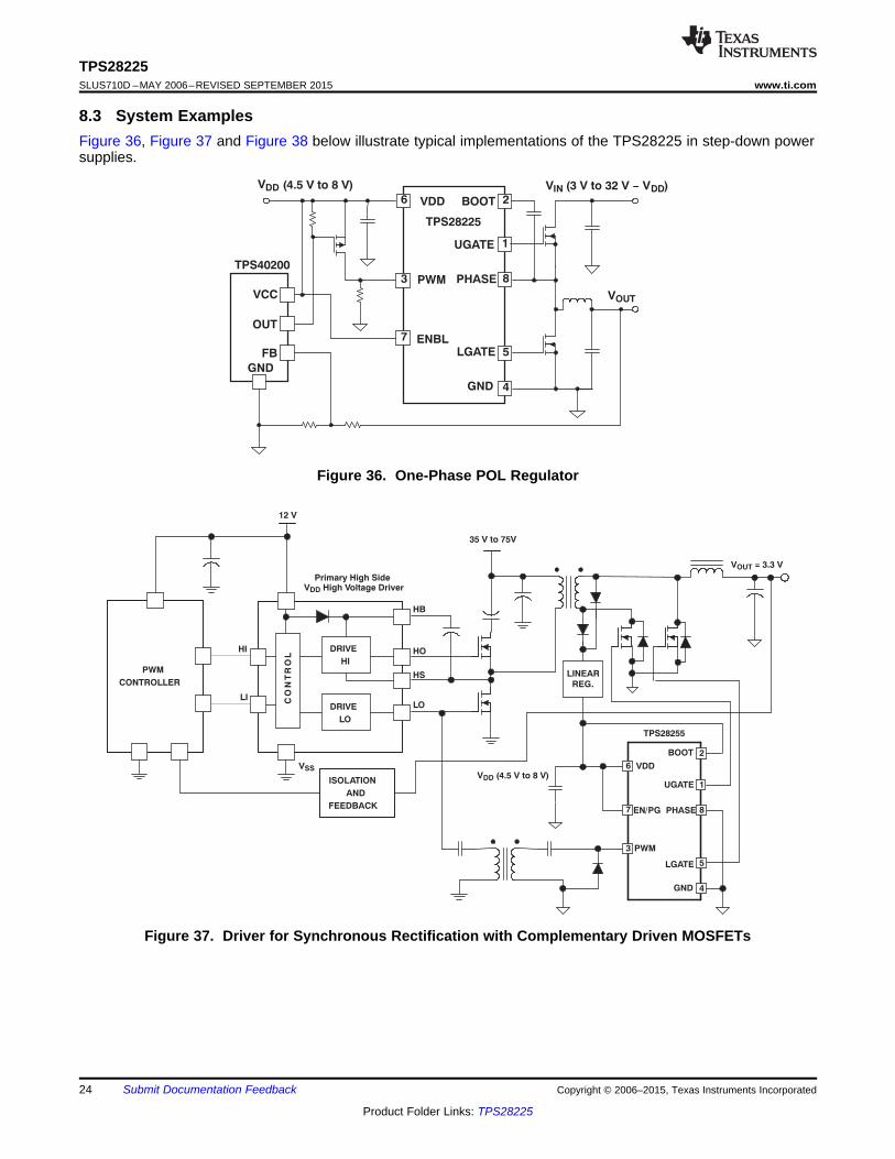
8.3 System ExamplesFigure 36, Figure 37 and Figure 38 below illustrate typical implementations of the TPS28225 in step-down powersupplies.
Figure 36. One-Phase POL Regulator
Figure 37. Driver for Synchronous Rectification with Complementary Driven MOSFETs
24 Submit Documentation Feedback Copyright © 2006–2015, Texas Instruments Incorporated
Product Folder Links: TPS28225

5
4
7 3
8
1
2
2BOOT
UGATE
PHASE
LGATE
GND
1
8
5
4
6 VDD
EN/PG7
PWM3
2BOOT
UGATE
PHASE
LGATE
GND
1
8
5
4
6 VDD
EN/PG7
PWM3
VIN
PWM 4
GND
VOUT
PWM1
8PWM3
Enable
PWM2
To Driver
To Driver
GNDS
To Controller
CSCNCS 4
To Controller
CS 1
VDD (4.5 V to 8 V) VIN (3 V to 32 V − VDD)
TPS28225
TPS28225
TP
S4009x
or
an
y o
ther
an
alo
go
r d
igit
al co
ntr
oller
VOUT
TPS28225www.ti.com SLUS710D –MAY 2006–REVISED SEPTEMBER 2015
System Examples (continued)
Figure 38. Multi-Phase Synchronous Buck Converter
Copyright © 2006–2015, Texas Instruments Incorporated Submit Documentation Feedback 25
Product Folder Links: TPS28225

TPS28225SLUS710D –MAY 2006–REVISED SEPTEMBER 2015 www.ti.com
9 Power Supply RecommendationsThe supply voltage range for operation is 4.5 to 8 V. The lower end of this range is governed by the under-voltage lockout thresholds. The UVLO disables the driver and keeps the power FETs OFF when VDD is too low.A lows ESR ceramic decoupling capacitor in the range of 0.22 µF to 4.7 µF between VDD and GND isrecommended.
10 Layout
10.1 Layout Guidelines
To improve the switching characteristics and efficiency of a design, the following layout rules need to be followed.• Locate the driver as close as possible to the MOSFETs.• Locate the VDD and bootstrap capacitors as close as possible to the driver.• Pay special attention to the GND trace. Use the thermal pad of the DFN-8 package as the GND by
connecting it to the GND pin. The GND trace or pad from the driver goes directly to the source of theMOSFET but should not include the high current path of the main current flowing through the drain andsource of the MOSFET.
• Use a similar rule for the PHASE node as for the GND.• Use wide traces for UGATE and LGATE closely following the related PHASE and GND traces. Eighty to 100
mils width is preferable where possible.• Use at least 2 or more vias if the MOSFET driving trace needs to be routed from one layer to another. For the
GND the number of vias are determined not only by the parasitic inductance but also by the requirements forthe thermal pad.
• Avoid PWM and enable traces going close to the PHASE node and pad where high dV/dT voltage can inducesignificant noise into the relatively high impedance leads.
It should be taken into account that poor layout can cause 3% to 5% less efficiency versus a good layout designand can even decrease the reliability of the whole system.
The schematic of one of the phases in a multi-phase synchronous buck regulator and the related layout areshown in Figure 25 and Figure 41. These help to illustrate good design practices. The power stage includes onehigh-side MOSFET Q10 and two low-side MOSFETS (Q8 and Q9). The driver (U7) is located on bottom side ofPCB close to the power MOSFETs. The related switching waveforms during turning ON and OFF of upper FETare shown in Figure 39 and Figure 40. The dead time during turning ON is only 10 ns (Figure 39) and 22 nsduring turning OFF (Figure 40).
Figure 40. Phase Falling-Edge Switching Waveforms (10Figure 39. Phase Rising-Edge Switching Waveforms (20ns/div) of the Power State in Figure 25ns/div) of the Power Stage in Figure 25
26 Submit Documentation Feedback Copyright © 2006–2015, Texas Instruments Incorporated
Product Folder Links: TPS28225

TPS28225www.ti.com SLUS710D –MAY 2006–REVISED SEPTEMBER 2015
10.2 Layout Example
Figure 41. Component Placement Based on Schematic in Figure 25
Copyright © 2006–2015, Texas Instruments Incorporated Submit Documentation Feedback 27
Product Folder Links: TPS28225

TPS28225SLUS710D –MAY 2006–REVISED SEPTEMBER 2015 www.ti.com
11 Device and Documentation Support
11.1 Device Support
11.1.1 Third-Party Products DisclaimerTI'S PUBLICATION OF INFORMATION REGARDING THIRD-PARTY PRODUCTS OR SERVICES DOES NOTCONSTITUTE AN ENDORSEMENT REGARDING THE SUITABILITY OF SUCH PRODUCTS OR SERVICESOR A WARRANTY, REPRESENTATION OR ENDORSEMENT OF SUCH PRODUCTS OR SERVICES, EITHERALONE OR IN COMBINATION WITH ANY TI PRODUCT OR SERVICE.
11.2 Documentation Support
11.2.1 Related Documentation• TPS40090, TPS40091 2/3/4-Phase Multi-Phase Controller, (SLUS578)
11.3 Community ResourcesThe following links connect to TI community resources. Linked contents are provided "AS IS" by the respectivecontributors. They do not constitute TI specifications and do not necessarily reflect TI's views; see TI's Terms ofUse.
TI E2E™ Online Community TI's Engineer-to-Engineer (E2E) Community. Created to foster collaborationamong engineers. At e2e.ti.com, you can ask questions, share knowledge, explore ideas and helpsolve problems with fellow engineers.
Design Support TI's Design Support Quickly find helpful E2E forums along with design support tools andcontact information for technical support.
11.4 TrademarksE2E is a trademark of Texas Instruments.All other trademarks are the property of their respective owners.
11.5 Electrostatic Discharge CautionThese devices have limited built-in ESD protection. The leads should be shorted together or the device placed in conductive foamduring storage or handling to prevent electrostatic damage to the MOS gates.
11.6 GlossarySLYZ022 — TI Glossary.
This glossary lists and explains terms, acronyms, and definitions.
12 Mechanical, Packaging, and Orderable InformationThe following pages include mechanical, packaging, and orderable information. This information is the mostcurrent data available for the designated devices. This data is subject to change without notice and revision ofthis document. For browser-based versions of this data sheet, refer to the left-hand navigation.
28 Submit Documentation Feedback Copyright © 2006–2015, Texas Instruments Incorporated
Product Folder Links: TPS28225

PACKAGE OPTION ADDENDUM
www.ti.com 29-Dec-2017
Addendum-Page 1
PACKAGING INFORMATION
Orderable Device Status(1)
Package Type PackageDrawing
Pins PackageQty
Eco Plan(2)
Lead/Ball Finish(6)
MSL Peak Temp(3)
Op Temp (°C) Device Marking(4/5)
Samples
TPS28225D ACTIVE SOIC D 8 75 Green (RoHS& no Sb/Br)
CU NIPDAU Level-1-260C-UNLIM -40 to 125 28225
TPS28225DG4 ACTIVE SOIC D 8 75 Green (RoHS& no Sb/Br)
CU NIPDAU Level-1-260C-UNLIM -40 to 125 28225
TPS28225DR ACTIVE SOIC D 8 2500 Green (RoHS& no Sb/Br)
CU NIPDAU Level-1-260C-UNLIM -40 to 125 28225
TPS28225DRBR ACTIVE SON DRB 8 3000 Green (RoHS& no Sb/Br)
CU NIPDAU Level-2-260C-1 YEAR -40 to 125 822565166
TPS28225DRBT ACTIVE SON DRB 8 250 Green (RoHS& no Sb/Br)
CU NIPDAU Level-2-260C-1 YEAR -40 to 125 822565166
TPS28226D ACTIVE SOIC D 8 75 Green (RoHS& no Sb/Br)
CU NIPDAU Level-1-260C-UNLIM -40 to 125 28226
TPS28226DG4 ACTIVE SOIC D 8 75 Green (RoHS& no Sb/Br)
CU NIPDAU Level-1-260C-UNLIM -40 to 125 28226
TPS28226DR ACTIVE SOIC D 8 2500 Green (RoHS& no Sb/Br)
CU NIPDAU Level-1-260C-UNLIM -40 to 125 28226
TPS28226DRBR ACTIVE SON DRB 8 3000 Green (RoHS& no Sb/Br)
CU NIPDAU Level-2-260C-1 YEAR -40 to 125 8226
TPS28226DRBT ACTIVE SON DRB 8 250 Green (RoHS& no Sb/Br)
CU NIPDAU Level-2-260C-1 YEAR -40 to 125 8226
(1) The marketing status values are defined as follows:ACTIVE: Product device recommended for new designs.LIFEBUY: TI has announced that the device will be discontinued, and a lifetime-buy period is in effect.NRND: Not recommended for new designs. Device is in production to support existing customers, but TI does not recommend using this part in a new design.PREVIEW: Device has been announced but is not in production. Samples may or may not be available.OBSOLETE: TI has discontinued the production of the device.
(2) RoHS: TI defines "RoHS" to mean semiconductor products that are compliant with the current EU RoHS requirements for all 10 RoHS substances, including the requirement that RoHS substancedo not exceed 0.1% by weight in homogeneous materials. Where designed to be soldered at high temperatures, "RoHS" products are suitable for use in specified lead-free processes. TI mayreference these types of products as "Pb-Free".RoHS Exempt: TI defines "RoHS Exempt" to mean products that contain lead but are compliant with EU RoHS pursuant to a specific EU RoHS exemption.Green: TI defines "Green" to mean the content of Chlorine (Cl) and Bromine (Br) based flame retardants meet JS709B low halogen requirements of <=1000ppm threshold. Antimony trioxide basedflame retardants must also meet the <=1000ppm threshold requirement.
(3) MSL, Peak Temp. - The Moisture Sensitivity Level rating according to the JEDEC industry standard classifications, and peak solder temperature.
PACKAGE OPTION ADDENDUM
www.ti.com 29-Dec-2017
Addendum-Page 2
(4) There may be additional marking, which relates to the logo, the lot trace code information, or the environmental category on the device.
(5) Multiple Device Markings will be inside parentheses. Only one Device Marking contained in parentheses and separated by a "~" will appear on a device. If a line is indented then it is a continuationof the previous line and the two combined represent the entire Device Marking for that device.
(6) Lead/Ball Finish - Orderable Devices may have multiple material finish options. Finish options are separated by a vertical ruled line. Lead/Ball Finish values may wrap to two lines if the finishvalue exceeds the maximum column width.
Important Information and Disclaimer:The information provided on this page represents TI's knowledge and belief as of the date that it is provided. TI bases its knowledge and belief on informationprovided by third parties, and makes no representation or warranty as to the accuracy of such information. Efforts are underway to better integrate information from third parties. TI has taken andcontinues to take reasonable steps to provide representative and accurate information but may not have conducted destructive testing or chemical analysis on incoming materials and chemicals.TI and TI suppliers consider certain information to be proprietary, and thus CAS numbers and other limited information may not be available for release.
In no event shall TI's liability arising out of such information exceed the total purchase price of the TI part(s) at issue in this document sold by TI to Customer on an annual basis.
OTHER QUALIFIED VERSIONS OF TPS28225 :
• Automotive: TPS28225-Q1
NOTE: Qualified Version Definitions:
• Automotive - Q100 devices qualified for high-reliability automotive applications targeting zero defects

TAPE AND REEL INFORMATION
*All dimensions are nominal
Device PackageType
PackageDrawing
Pins SPQ ReelDiameter
(mm)
ReelWidth
W1 (mm)
A0(mm)
B0(mm)
K0(mm)
P1(mm)
W(mm)
Pin1Quadrant
TPS28225DR SOIC D 8 2500 330.0 12.4 6.4 5.2 2.1 8.0 12.0 Q1
TPS28225DRBR SON DRB 8 3000 330.0 12.4 3.3 3.3 1.1 8.0 12.0 Q2
TPS28225DRBT SON DRB 8 250 180.0 12.4 3.3 3.3 1.1 8.0 12.0 Q2
TPS28226DR SOIC D 8 2500 330.0 12.4 6.4 5.2 2.1 8.0 12.0 Q1
TPS28226DRBR SON DRB 8 3000 330.0 12.4 3.3 3.3 1.1 8.0 12.0 Q2
TPS28226DRBT SON DRB 8 250 180.0 12.4 3.3 3.3 1.1 8.0 12.0 Q2
PACKAGE MATERIALS INFORMATION
www.ti.com 2-Feb-2018
Pack Materials-Page 1

*All dimensions are nominal
Device Package Type Package Drawing Pins SPQ Length (mm) Width (mm) Height (mm)
TPS28225DR SOIC D 8 2500 340.5 338.1 20.6
TPS28225DRBR SON DRB 8 3000 367.0 367.0 35.0
TPS28225DRBT SON DRB 8 250 210.0 185.0 35.0
TPS28226DR SOIC D 8 2500 340.5 338.1 20.6
TPS28226DRBR SON DRB 8 3000 367.0 367.0 35.0
TPS28226DRBT SON DRB 8 250 210.0 185.0 35.0
PACKAGE MATERIALS INFORMATION
www.ti.com 2-Feb-2018
Pack Materials-Page 2


www.ti.com
PACKAGE OUTLINE
C
8X 0.370.25
1.75 0.12X
1.95
1.5 0.1
6X 0.65
1 MAX
8X 0.50.3
0.050.00
(0.65)
A 3.12.9
B
3.12.9
(DIM A) TYP4X (0.23)
VSON - 1 mm max heightDRB0008APLASTIC SMALL OUTLINE - NO LEAD
4218875/A 01/2018
DIM AOPT 1 OPT 2(0.1) (0.2)
PIN 1 INDEX AREA
SEATING PLANE
0.08 C
1
4 5
8
(OPTIONAL)PIN 1 ID 0.1 C A B
0.05 C
THERMAL PADEXPOSED
NOTES: 1. All linear dimensions are in millimeters. Any dimensions in parenthesis are for reference only. Dimensioning and tolerancing per ASME Y14.5M. 2. This drawing is subject to change without notice. 3. The package thermal pad must be soldered to the printed circuit board for thermal and mechanical performance.
SCALE 4.000

www.ti.com
EXAMPLE BOARD LAYOUT
0.07 MINALL AROUND
0.07 MAXALL AROUND
8X (0.31)
(1.75)
(2.8)
6X (0.65)
(1.5)
( 0.2) VIATYP
(0.5)
(0.625)
8X (0.6)
(R0.05) TYP
(0.825)
(0.23)
(0.65)
VSON - 1 mm max heightDRB0008APLASTIC SMALL OUTLINE - NO LEAD
4218875/A 01/2018
SYMM
1
45
8
LAND PATTERN EXAMPLEEXPOSED METAL SHOWN
SCALE:20X
NOTES: (continued) 4. This package is designed to be soldered to a thermal pad on the board. For more information, see Texas Instruments literature number SLUA271 (www.ti.com/lit/slua271).5. Vias are optional depending on application, refer to device data sheet. If any vias are implemented, refer to their locations shown on this view. It is recommended that vias under paste be filled, plugged or tented.
SYMM
SOLDER MASKOPENINGSOLDER MASK
METAL UNDER
SOLDER MASKDEFINED
EXPOSEDMETAL
METALSOLDER MASKOPENING
SOLDER MASK DETAILS
NON SOLDER MASKDEFINED
(PREFERRED)
EXPOSEDMETAL

www.ti.com
EXAMPLE STENCIL DESIGN
(R0.05) TYP
8X (0.31)
8X (0.6)
(1.34)
(1.55)
(2.8)
6X (0.65)
4X(0.725)
4X (0.23)
(2.674)
(0.65)
VSON - 1 mm max heightDRB0008APLASTIC SMALL OUTLINE - NO LEAD
4218875/A 01/2018
NOTES: (continued) 6. Laser cutting apertures with trapezoidal walls and rounded corners may offer better paste release. IPC-7525 may have alternate design recommendations.
SOLDER PASTE EXAMPLEBASED ON 0.125 mm THICK STENCIL
EXPOSED PAD
84% PRINTED SOLDER COVERAGE BY AREASCALE:25X
SYMM
1
45
8
METALTYP
SYMM


IMPORTANT NOTICE
Texas Instruments Incorporated (TI) reserves the right to make corrections, enhancements, improvements and other changes to itssemiconductor products and services per JESD46, latest issue, and to discontinue any product or service per JESD48, latest issue. Buyersshould obtain the latest relevant information before placing orders and should verify that such information is current and complete.TI’s published terms of sale for semiconductor products (http://www.ti.com/sc/docs/stdterms.htm) apply to the sale of packaged integratedcircuit products that TI has qualified and released to market. Additional terms may apply to the use or sale of other types of TI products andservices.Reproduction of significant portions of TI information in TI data sheets is permissible only if reproduction is without alteration and isaccompanied by all associated warranties, conditions, limitations, and notices. TI is not responsible or liable for such reproduceddocumentation. Information of third parties may be subject to additional restrictions. Resale of TI products or services with statementsdifferent from or beyond the parameters stated by TI for that product or service voids all express and any implied warranties for theassociated TI product or service and is an unfair and deceptive business practice. TI is not responsible or liable for any such statements.Buyers and others who are developing systems that incorporate TI products (collectively, “Designers”) understand and agree that Designersremain responsible for using their independent analysis, evaluation and judgment in designing their applications and that Designers havefull and exclusive responsibility to assure the safety of Designers' applications and compliance of their applications (and of all TI productsused in or for Designers’ applications) with all applicable regulations, laws and other applicable requirements. Designer represents that, withrespect to their applications, Designer has all the necessary expertise to create and implement safeguards that (1) anticipate dangerousconsequences of failures, (2) monitor failures and their consequences, and (3) lessen the likelihood of failures that might cause harm andtake appropriate actions. Designer agrees that prior to using or distributing any applications that include TI products, Designer willthoroughly test such applications and the functionality of such TI products as used in such applications.TI’s provision of technical, application or other design advice, quality characterization, reliability data or other services or information,including, but not limited to, reference designs and materials relating to evaluation modules, (collectively, “TI Resources”) are intended toassist designers who are developing applications that incorporate TI products; by downloading, accessing or using TI Resources in anyway, Designer (individually or, if Designer is acting on behalf of a company, Designer’s company) agrees to use any particular TI Resourcesolely for this purpose and subject to the terms of this Notice.TI’s provision of TI Resources does not expand or otherwise alter TI’s applicable published warranties or warranty disclaimers for TIproducts, and no additional obligations or liabilities arise from TI providing such TI Resources. TI reserves the right to make corrections,enhancements, improvements and other changes to its TI Resources. TI has not conducted any testing other than that specificallydescribed in the published documentation for a particular TI Resource.Designer is authorized to use, copy and modify any individual TI Resource only in connection with the development of applications thatinclude the TI product(s) identified in such TI Resource. NO OTHER LICENSE, EXPRESS OR IMPLIED, BY ESTOPPEL OR OTHERWISETO ANY OTHER TI INTELLECTUAL PROPERTY RIGHT, AND NO LICENSE TO ANY TECHNOLOGY OR INTELLECTUAL PROPERTYRIGHT OF TI OR ANY THIRD PARTY IS GRANTED HEREIN, including but not limited to any patent right, copyright, mask work right, orother intellectual property right relating to any combination, machine, or process in which TI products or services are used. Informationregarding or referencing third-party products or services does not constitute a license to use such products or services, or a warranty orendorsement thereof. Use of TI Resources may require a license from a third party under the patents or other intellectual property of thethird party, or a license from TI under the patents or other intellectual property of TI.TI RESOURCES ARE PROVIDED “AS IS” AND WITH ALL FAULTS. TI DISCLAIMS ALL OTHER WARRANTIES ORREPRESENTATIONS, EXPRESS OR IMPLIED, REGARDING RESOURCES OR USE THEREOF, INCLUDING BUT NOT LIMITED TOACCURACY OR COMPLETENESS, TITLE, ANY EPIDEMIC FAILURE WARRANTY AND ANY IMPLIED WARRANTIES OFMERCHANTABILITY, FITNESS FOR A PARTICULAR PURPOSE, AND NON-INFRINGEMENT OF ANY THIRD PARTY INTELLECTUALPROPERTY RIGHTS. TI SHALL NOT BE LIABLE FOR AND SHALL NOT DEFEND OR INDEMNIFY DESIGNER AGAINST ANY CLAIM,INCLUDING BUT NOT LIMITED TO ANY INFRINGEMENT CLAIM THAT RELATES TO OR IS BASED ON ANY COMBINATION OFPRODUCTS EVEN IF DESCRIBED IN TI RESOURCES OR OTHERWISE. IN NO EVENT SHALL TI BE LIABLE FOR ANY ACTUAL,DIRECT, SPECIAL, COLLATERAL, INDIRECT, PUNITIVE, INCIDENTAL, CONSEQUENTIAL OR EXEMPLARY DAMAGES INCONNECTION WITH OR ARISING OUT OF TI RESOURCES OR USE THEREOF, AND REGARDLESS OF WHETHER TI HAS BEENADVISED OF THE POSSIBILITY OF SUCH DAMAGES.Unless TI has explicitly designated an individual product as meeting the requirements of a particular industry standard (e.g., ISO/TS 16949and ISO 26262), TI is not responsible for any failure to meet such industry standard requirements.Where TI specifically promotes products as facilitating functional safety or as compliant with industry functional safety standards, suchproducts are intended to help enable customers to design and create their own applications that meet applicable functional safety standardsand requirements. Using products in an application does not by itself establish any safety features in the application. Designers mustensure compliance with safety-related requirements and standards applicable to their applications. Designer may not use any TI products inlife-critical medical equipment unless authorized officers of the parties have executed a special contract specifically governing such use.Life-critical medical equipment is medical equipment where failure of such equipment would cause serious bodily injury or death (e.g., lifesupport, pacemakers, defibrillators, heart pumps, neurostimulators, and implantables). Such equipment includes, without limitation, allmedical devices identified by the U.S. Food and Drug Administration as Class III devices and equivalent classifications outside the U.S.TI may expressly designate certain products as completing a particular qualification (e.g., Q100, Military Grade, or Enhanced Product).Designers agree that it has the necessary expertise to select the product with the appropriate qualification designation for their applicationsand that proper product selection is at Designers’ own risk. Designers are solely responsible for compliance with all legal and regulatoryrequirements in connection with such selection.Designer will fully indemnify TI and its representatives against any damages, costs, losses, and/or liabilities arising out of Designer’s non-compliance with the terms and provisions of this Notice.
Mailing Address: Texas Instruments, Post Office Box 655303, Dallas, Texas 75265Copyright © 2018, Texas Instruments Incorporated