tps2358 dual-slotatca advancedmc™ controller€¢ latch off after fault that allow an external fet...
TRANSCRIPT

PG
12
A\
EN
12A
\
FL
T1
2A
\
PASSA
OUT12A
BLKA
EN
3A
\
AG
ND
IN3
A
FL
T3A
\
PG
3A
\
PG
12B
\E
N1
2B
\
FLT
12B
\
TPS2358
48 PIN QFN
EN
3B
\
3v3 in
CT
12B
VD
D3
B
FL
T3B
\
PG
3B
\
RSENSE
RSET
IN12B
COMMON
CIRCUITRY
3v3 in 12 Vin B
IN12AIN3
B
VD
D3A
AG
ND
GN
D
OR
EN
B\
VIN
T
OR
EN
A\
CT
3B
CT
12A
CT
3A
GN
DB
GN
DA
SENMB
PASSB
OUT12B
SETB
BLKB
SENPB
SU
M3
B
SU
M1
2B
RS
UM
3B R
SU
M1
2B
12 Vin A
Optional ORing elements forRedundant Systems Only
OUT3B
AdvancedMC ™
12 V 3.3 V
OUT3A
AdvancedMC ™
12 V3.3 V
SU
M3
A
SU
M1
2A
RSUM3A
RSUM12A
100
100
100
1 uF 1 uF
SENMA
SETA
SENPA
100
RSET
RSENSE
TPS2358
www.ti.com SLUS820E –FEBRUARY 2008–REVISED NOVEMBER 2009
TPS2358 Dual-Slot ATCA AdvancedMC™ ControllerCheck for Samples: TPS2358
1FEATURESDESCRIPTION
2• ATCA AdvancedMC™ Compliant• Full Power Control for Two The TPS2358 dual-slot hot-plug controller provides all
required power interface functions for twoAdvancedMC™ModulesAdvancedMC™ (Advanced Mezzanine Card)• Independent 12-V Current Limit and Fast Tripmodules.
• 12-V FET ORing for MicroTCA™Two fully integrated 3.3-V channels provide inrush• Internal 3.3-V Current Limitcontrol, current limiting, and overload protection. The
• Power Good and Fault Outputs two 12-V channels use an external FET to providethe same functions, along with ORing control circuits• 48-Pin PQFN Packagethat allow an external FET to prevent reverse current• Latch Off After Faultflow. External capacitors are used to set fault times.There is one capacitor for each channel. The 3.3-VAPPLICATIONS current limits are factory set to AdvancedMC™
• ATCA Carrier Boards compliant levels and the 12-V current limits are• MicroTCA™ Power Modules programmed using external sense resistors. The
accurate current sense comparators of the TPS2358• AdvancedMC™ Slotssatisfy the narrow ATCA AdvancedMC™ current limit• Systems Using 12 V and 3.3 Vrequirements.
• Base Stations
TYPICAL APPLICATION DIAGRAM
1
Please be aware that an important notice concerning availability, standard warranty, and use in critical applications of TexasInstruments semiconductor products and disclaimers thereto appears at the end of this data sheet.
2AdvancedMC, MicroTCA are trademarks of PICMG.
PRODUCTION DATA information is current as of publication date. Copyright © 2008–2009, Texas Instruments IncorporatedProducts conform to specifications per the terms of the TexasInstruments standard warranty. Production processing does notnecessarily include testing of all parameters.
TPS2358
SLUS820E –FEBRUARY 2008–REVISED NOVEMBER 2009 www.ti.com
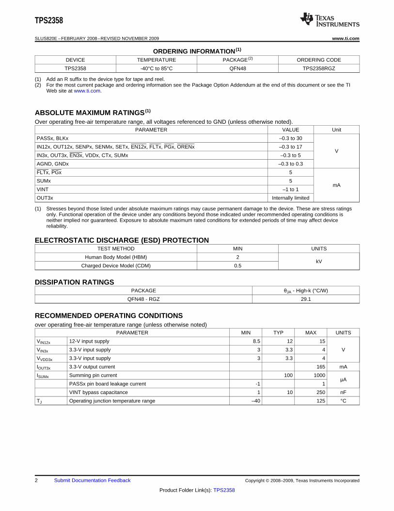
ORDERING INFORMATION (1)
DEVICE TEMPERATURE PACKAGE (2) ORDERING CODE
TPS2358 -40°C to 85°C QFN48 TPS2358RGZ
(1) Add an R suffix to the device type for tape and reel.(2) For the most current package and ordering information see the Package Option Addendum at the end of this document or see the TI
Web site at www.ti.com.
ABSOLUTE MAXIMUM RATINGS (1)
Over operating free-air temperature range, all voltages referenced to GND (unless otherwise noted).PARAMETER VALUE Unit
PASSx, BLKx –0.3 to 30
IN12x, OUT12x, SENPx, SENMx, SETx, EN12x, FLTx, PGx, ORENx –0.3 to 17V
IN3x, OUT3x, EN3x, VDDx, CTx, SUMx –0.3 to 5
AGND, GNDx –0.3 to 0.3
FLTx, PGx 5
SUMx 5mA
VINT –1 to 1
OUT3x Internally limited
(1) Stresses beyond those listed under absolute maximum ratings may cause permanent damage to the device. These are stress ratingsonly. Functional operation of the device under any conditions beyond those indicated under recommended operating conditions isneither implied nor guaranteed. Exposure to absolute maximum rated conditions for extended periods of time may affect devicereliability.
ELECTROSTATIC DISCHARGE (ESD) PROTECTIONTEST METHOD MIN UNITS
Human Body Model (HBM) 2kV
Charged Device Model (CDM) 0.5
DISSIPATION RATINGSPACKAGE θJA - High-k (°C/W)
QFN48 - RGZ 29.1
RECOMMENDED OPERATING CONDITIONSover operating free-air temperature range (unless otherwise noted)
PARAMETER MIN TYP MAX UNITS
VIN12x 12-V input supply 8.5 12 15
VIN3x 3.3-V input supply 3 3.3 4 V
VVDD3x 3.3-V input supply 3 3.3 4
IOUT3x 3.3-V output current 165 mA
ISUMx Summing pin current 100 1000μA
PASSx pin board leakage current -1 1
VINT bypass capacitance 1 10 250 nF
TJ Operating junction temperature range –40 125 °C
2 Submit Documentation Feedback Copyright © 2008–2009, Texas Instruments Incorporated
Product Folder Link(s): TPS2358

TPS2358
www.ti.com SLUS820E –FEBRUARY 2008–REVISED NOVEMBER 2009
ELECTRICAL CHARACTERISTICSIN3A = IN3B = VDD3A = VDD3B = 3.3 V. IN12A = IN12B = SENPA = SENPB = SENMA = SENMB = SETPA =SETPB = 12 V. EN12A = EN12B = EN3A = EN3B = ORENA = ORENB = CT12A = CT12B = CT3A = CT3B = AGND =GNDA = GNDB = 0 V. SUM12A = SUM12B = 6.8 kΩ to ground. SUM3A = SUM3B = 3.3 kΩ to ground. All other pins open.Over free air temperature operating range and all voltages referenced to AGND, -40°C ≤ TA ≤ 85°C, typical vales at 25°C,unless otherwise noted.
PARAMETER CONDITIONS MIN TYP MAX UNITS
ENABLE Inputs
Threshold voltage, falling 1.2 1.3 1.4 Vedge
Hysteresis 20 50 80 mV
Pullup current ENx = ORENx = 0 V 5 8 15
Input bias current EN12x = ORENx = 17 V 6 15 μA
Input bias current EN3x = 5 V 1 5
3.3-V turn off time EN3x deasserts to VOUT3x < 1.0 V, COUT = 0 μF 10μsEN12x deasserts to VOUT12x < 1.0 V, COUT = 0 μF,12-V turn off time 20QGATE = 35 nF
POWER GOOD Outputs
Low voltage Sinking 2 mA 0.14 0.25 V
Leakage current PGx = 17 V 1 μA
Threshold voltage PG12x, falling VOUT12x 10.2 10.5 10.8V
PG3x, falling VOUT3x 2.7 2.8 2.9
Hysteresis PG12x, measured at OUT12x 130mV
PG3x, measured at OUT3x 50
Deglitch time PGx falling 50 100 150 μs
FAULT Outputs
Low voltage Sinking 2 mA 0.14 0.25 V
Leakage current PGx = 17 V 1 μA
VINT
Output voltage 0 < IVINT < 50 μA 2 2.3 2.8 V
Fault Timer
Sourcing current VCTx = 0 V, during fault –7 –10 –13μA
Sinking current VCTx = 2 V 7 10 13
Upper threshold voltage 1.3 1.35 1.4V
Lower threshold voltage 0.33 0.35 0.37
12-V Summing Node
VSENMx = 10.8 – 13.2 V, VSENPx = VSENMx + 50 mV,Input referred offset –2 2 mVmeasure VSETx – VSENMx
Summing threshold VPASSx = 15 V 0.66 0.675 0.69 V
Leakage current VSETx = VSENMx – 10 mV 1 μA
12-V Current Limit
RSUMx = 6.8 kΩ, RSETx = 422 Ω, increase ILOADx andCurrent limit threshold 47.5 50 52.5 mVmeasure VSENPx – VSENMx when VPASSx = 15 V
Sink current in current VSUMx = 1 V, VPASSx = 12 V, measure IPASSx 20 40 μAlimit
Fast trip threshold Measure VSENPx – VSENMx 80 100 120 mV
Fast turn-off delay 20 mV overdrive, CPASSx = 0 pF, tp50-50 200 300 ns
VPASSx - VINx when timer starts, while VPASSx fallingTimer start threshold 5 6 7 Vdue to over current
Copyright © 2008–2009, Texas Instruments Incorporated Submit Documentation Feedback 3
Product Folder Link(s): TPS2358

TPS2358
SLUS820E –FEBRUARY 2008–REVISED NOVEMBER 2009 www.ti.com
ELECTRICAL CHARACTERISTICS (continued)IN3A = IN3B = VDD3A = VDD3B = 3.3 V. IN12A = IN12B = SENPA = SENPB = SENMA = SENMB = SETPA =SETPB = 12 V. EN12A = EN12B = EN3A = EN3B = ORENA = ORENB = CT12A = CT12B = CT3A = CT3B = AGND =GNDA = GNDB = 0 V. SUM12A = SUM12B = 6.8 kΩ to ground. SUM3A = SUM3B = 3.3 kΩ to ground. All other pins open.Over free air temperature operating range and all voltages referenced to AGND, -40°C ≤ TA ≤ 85°C, typical vales at 25°C,unless otherwise noted.
PARAMETER CONDITIONS MIN TYP MAX UNITS
12-V UVLO
UVLO rising IN12x rising 8.1 8.5 8.9V
UVLO hysteresis IN12x falling 0.44 0.5 0.59
12-V BLOCKING
Turn-on threshold Measure VSENPx – VOUTx 5 10 15mV
Turn-off threshold Measure VSENPx – VOUTx –5 –3 0
Turn-off delay 20 mV overdrive, CBLKx = 0 pF, tp50-50 200 300 ns
12-V Gate Drivers ( PASSx, BLKx )
Output voltage VINx = VOUTx = 10 V 21.5 23 24.5 V
Sourcing current VIN12x = VOUT12x = 10 V, VPASSx = VBLKx = 17 V 20 30 40 μA
Fast turnoff, VPASSx = VBLKx = 14 V 0.5 1 ASinking current
Sustained, VPASSx = VBLKx = 4 – 25 V 6 14 25 mA
Pulldown resistance In OTSD ( at 150 °C ) 14 20 26 kΩFast turn-off duration 5 10 15 μs
Disable delay EN12x pin to PASSx and BLKx, tp50-90 1 μs
Startup time IN12x rising to PASSx and BLKx sourcing 0.25 ms
3.3-V Summing Node
Summing threshold 655 675 695 mV
3.3-V Current Limit
On resistance IOUT3x = 150 mA 290 500 mΩCurrent limit RSUM3x = 3.3 kΩ , VOUT3x = 0 V 170 195 225
mAFast trip threshold 250 300 400
Fast turn-off delay IOUT3x = 400 mA, tp50-50 750 1300 ns
3.3-V UVLO
UVLO rising IN3x rising 2.65 2.75 2.85 V
UVLO hysteresis IN3x falling 200 240 300 mV
Supply Currents (IINx + ISENPx + ISENMx + ISETx + IVDDx)
All channels enabled IOUT3A = IOUT3B = 0 3.1 4mA
All channels disabled 2 2.8
Thermal Shutdown
Whole-chip shutdown TJ rising, IOUT3A = IOUT3B = 0 140 150temperature
3.3 V channel shutdown °CTJ rising, IOUT3A or IOUT3B in current limit 130 140temperature
Hysteresis Whole chip or 3.3-V channel 10
4 Submit Documentation Feedback Copyright © 2008–2009, Texas Instruments Incorporated
Product Folder Link(s): TPS2358

+
+
+
+
R SENSE
100 mv
675 mV
Fault
TimerVcp
30 uA
12dis
10 us
68
10
FLT12x\
10 mv
-3 mv S
Q
Q
RPG12x\
10 us
pgat\
ogat
OUT12xBLKxPASSxSETx SENMxSENPx
100 us
IN12x
OUT12x
pgat\
oren
+
30 uA
RSET
EN12x\
SUM12x
CT12x
PG3x\
Q
Pump
Vcp
~25 v
60 m A
ogat
+
OUT12x
vpg
100 100
TPS2358
www.ti.com SLUS820E –FEBRUARY 2008–REVISED NOVEMBER 2009
DEVICE INFORMATION
SIGNAL AND PIN NAMING BLOCK
The PICMG™ AdvancedMC™ specification refers to 3.3-V power as management power and refers to 12-Vpower as payload power. This datasheet uses a naming convention that reflects the associated voltage (12 V to3 V) and AdvancedMC™ slot (A or B).• Signals and pins associated with slot A 12-V payload power end with 12A.• Signals and pins associated with slot A 3.3-V management power end with 3A.• Signals and pins associated with slot B 12-V payload power end with 12B.• Signals and pins associated with slot B 3.3-V management power end with 3B.
Pins and signals unique to 12-V channels have only an A or B suffix.
TPS2358 Block Diagrams
Figure 1. 12-V Channel Circuitry
Copyright © 2008–2009, Texas Instruments Incorporated Submit Documentation Feedback 5
Product Folder Link(s): TPS2358

+
+
0.1 W
30 mv
Fault
Timer
3300
OUT3IN3
96 W
QPump
vcp~25 v
VDD3+
30 us
2.8 V
EN3
gat
en
30 us
Control
LogicSUM3
FLT3x \
PG3x\
675 mV
+
60 mA
30 uA
IN12A
IN12B
IN3A
IN3B
OUT12A
OUT12B
OUT3A
OUT3B
PREREG
VINT
2.2 V
POR
en por
ControlLogic
GNDB
GNDA
AGND
TPS2358
SLUS820E –FEBRUARY 2008–REVISED NOVEMBER 2009 www.ti.com
Figure 2. 3-V Channel Circuitry
Figure 3. Circuitry Common to all Channels
6 Submit Documentation Feedback Copyright © 2008–2009, Texas Instruments Incorporated
Product Folder Link(s): TPS2358

IN12A
SENPA
SENMA
PG12A
GND
VD
D3A
12A, 12B
3A, 3B
Control
SETA
VINT
SUM12A
IN3A
CT3AC
T12A
FLT3A
ORENA
PG12B
GND
PG3A
SUM3A
IN12B
SE
NP
B
SE
NM
B
PA
SS
B
OR
EN
B
FLT
12B
SE
TB
BLK
B
IN3B
SUM3B
OU
T12B
VDD3B
PG3B
OUT3A
FLT3B
CT3B
OUT3B
CT
12B
SUM12B
EN
12A
EN
12B
EN
3A
BLK
A
FLT
12A
OU
T12A
EN
3B
48 Pin QFN
PA
SS
A
GN
DA
GN
DB
AGND
48 47 46 45 44 43 42 41 40 39 38 37
13 14 15 16 17 18 19 20 21 22 23 24
1
3
4
5
6
7
8
9
10
11
12
36
35
34
33
32
31
30
29
28
27
26
25
2
TPS2358
www.ti.com SLUS820E –FEBRUARY 2008–REVISED NOVEMBER 2009
TERMINAL FUNCTIONSPIN# NAME TYPE DESCRIPTION
1 IN12A VDD 12A input
2 SENPA I 12A input sense
3 SETA I 12A current limit set
4 SENMA I 12A current limit sense
5 VINT I/O Bypass capacitor connection point for internal supply
6 PG12A O 12A power good output, active low, asserts when OUT12A > VPG12A
7 SUM12A I/O 12A summing node
8 ORENA I 12A blocking transistor enable, active low
9 GND GND Connect pin to ground
10 GND GND Connect pin to ground
11 PG12B O 12B power good output, active low, asserts when OUT12B > VPG12B
12 SUM12B I/O 12B summing node
Copyright © 2008–2009, Texas Instruments Incorporated Submit Documentation Feedback 7
Product Folder Link(s): TPS2358

TPS2358
SLUS820E –FEBRUARY 2008–REVISED NOVEMBER 2009 www.ti.com
TERMINAL FUNCTIONS (continued)
PIN# NAME TYPE DESCRIPTION
13 CT12B I/O 12B fault timing capacitor
14 FLT12B O 12B fault output, active low, asserted when 12B fault timer runs out
15 BLKB O 12B blocking transistor gate drive
16 OUT12B I/O 12B output
17 GNDB GND 12B power ground
18 ORENB I 12B blocking transistor enable, active low
19 PASSB O 12B pass transistor gate drive
20 SENMB I 12B current limit sense
21 SETB I 12B current limit set
22 SENPB I 12B input sense
23 IN12B VDD 12B input
24 IN3B VDD 3B input
25 OUT3B I/O 3B output
26 CT3B I/O 3B fault timing capacitor
27 FLT3B O 3B fault output, active low, asserted when 3B fault timer runs out
28 PG3B O 3B power good output, active low, asserts when OUT3B > 2.8 V
29 SUM3B I/O 3B summing node
30 VDD3B VDD 3B charge pump input
31 AGND GND Analog ground
32 SUM3A I/O 3A summing node
33 PG3A O 3A power good output, active low, asserts when OUT3A > 2.8 V
34 FLT3A O 3A fault output, active low, asserted when 3A fault timer runs out
35 CT3A I/O 3A fault timing capacitor
36 OUT3A I/O 3A output
37 IN3A VDD 3A input
38 VDD3A VDD 3A charge pump input
39 EN3B I 3B enable, (default active low)
40 EN3A I 3A enable, (default active low)
41 EN12B I 12B enable, (default active low)
42 PASSA O 12A pass transistor gate drive
43 EN12A I 12A enable, (default active low)
44 GNDA GND 12A power ground
45 OUT12A I/O 12A output
46 BLKA O 12A blocking transistor gate drive
47 FLT12A I/O 12A fault output, active low, asserted when 12A fault timer runs out
48 CT12A I/O 12A fault timing capacitor
8 Submit Documentation Feedback Copyright © 2008–2009, Texas Instruments Incorporated
Product Folder Link(s): TPS2358

TPS2358
www.ti.com SLUS820E –FEBRUARY 2008–REVISED NOVEMBER 2009
DEVICE INFORMATION
DETAILED PIN DESCRIPTION
AGND Ground pin for the analog circuitry inside the TPS2358.
BLKx Gate drive pin for the 12x channel BLK FET. This pin sources 30 μA to turn the FET on. An internal clampprevents this pin from rising more than 14.5 V above OUT12x. Setting the ORENx pin high holds the BLKx pinlow.
CTx A capacitor from CTx to GND sets the time the channel can remain in current limit before it shuts down anddeclares a fault. Current limit causes this pin to source 10 μA into the external capacitor (CT). When VCTxreaches 1.35 V, the TPS2358 shuts the channel off by pulling the PASSx pin low and declares an over-currentfault by pulling the FLTx pin low.
EN12x Active low enable input. Pulling this pin high (or allowing it to float high) turns off channel 12x by pullingboth BLKx and PASSx low. An internal 200-kΩ resistor pulls this pin up to VINT when disconnected.
EN3x Active low enable input. Pulling this pin high (or allowing it to float high) turns off channel 3x by pulling thegate of the internal pass FET to GND. An internal 200-kΩ resistor pulls this pin up to VINT when disconnected.
FLTx Active low open-drain output indicating that channel x has remained in current limit long enough to time outthe fault timer and shut the channel down.
IN12x Supply pin for channel 12x internal circuitry.
IN3x Supply pin for channel 3x internal pass FET.
ORENx Active low input. Pulling this pin low allows the 12x channel ORing function to operate normally. Pullingthis pin high (or allowing it to float high) disables the ORing function by pulling the BLKx pin low. An internal200-kΩ resistor pulls this pin up to VINT when disconnected.
OUT12x Senses the output voltage of the channel 12x path. OUT12x is the return node for the BLKx pin clamp.This pin will source ~30 µA when the BLK FET is fully enhanced.
OUT3x Output of the channel 3x internal pass FET.
PASSx Gate drive pin for the 12x channel pass FET. This pin sources 30 μA to turn the FET on. An internalclamp prevents this pin from rising more than 14.5 V above IN12x.
PGx Active low open-drain output indicating that channel x output voltage is above the PG threshold, whichnominally equals 2.85 V for the 3x channels and 10.5 V for the 12x channels.
SENMx Senses the voltage on the low side of the channel 12x current sense resistor.
SENPx Senses the voltage on the high side of the channel 12x current sense resistor.
SETx A resistor connected from this pin to SENPx sets the current limit level in conjunction with the currentsense resistor and the resistor connected to the SUM12x pin, as described in 12-V thresholds – setting currentlimit and fast over current trip section.
SUMx A resistor connected from this pin to ground forms part of the channel x current limit. As the currentdelivered to the load increases, so does the voltage on this pin. When the voltage on this pin reaches a thresholdof 675 mV, the current limit amplifier acts to prevent the current from further increasing.
VDD3x Supply pin for channel3x internal circuitry.
VINT This pin connects to the internal 2.35-V rail. A 0.1-μF capacitor must be connected from this pin to ground.Do not connect other external circuitry to this pin.
Copyright © 2008–2009, Texas Instruments Incorporated Submit Documentation Feedback 9
Product Folder Link(s): TPS2358
-50 0 100 150
TJ
- Temperature - °C
50.0
50.2
51.0
50
50.6
50.8
mV
12-V CURRENT LIMIT THRESHOLD
50.4
-50 0 100 150
TJ
- Temperature
2.10
2.20
2.45
50
2.30
2.35
I DD
-m
A
3VIDD
vs
TEMPERATURE
2.15
2.25
2.40
-50 0 100 150
TJ
- Temperature - °C
-5.0
-4.0
0.0
50
-3.0
-1.0
mV
12-V CHANNEL ORING TURN-OFF THRESHOLD
-2.0
-50 0 100 150
TJ
- Temperature - °C
0.20
0.22
0.26
50
0.23
0.25
I DD
-m
A
3-V IDD
vs
TEMPERATURE
0.24
0.21
TPS2358
SLUS820E –FEBRUARY 2008–REVISED NOVEMBER 2009 www.ti.com
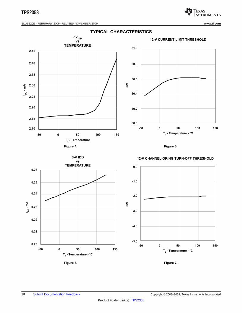
TYPICAL CHARACTERISTICS
Figure 4. Figure 5.
Figure 6. Figure 7.
10 Submit Documentation Feedback Copyright © 2008–2009, Texas Instruments Incorporated
Product Folder Link(s): TPS2358

-50 0 100 150
TJ
- Temperature - °C
8.0
9.0
12.0
50
10.0
11.0
mV
12-V CHANNEL ORING TURN-ON THRESHOLD
8.5
9.5
10.5
11.5
-50 0 100 150
TJ
- Temperature - °C
2.0
2.1
2.4
50
2.2
2.3
Cu
rre
nt
-m
A
12-V CURRENT (mA)
vs
TEMPERATURE
6
TPS2358
www.ti.com SLUS820E –FEBRUARY 2008–REVISED NOVEMBER 2009
TYPICAL CHARACTERISTICS (continued)
Figure 8. Figure 9.
Figure 10. OUT3A Startup Into 22-Ω ( 150 mA ) 150-μF Load
Copyright © 2008–2009, Texas Instruments Incorporated Submit Documentation Feedback 11
Product Folder Link(s): TPS2358
TPS2358
SLUS820E –FEBRUARY 2008–REVISED NOVEMBER 2009 www.ti.com
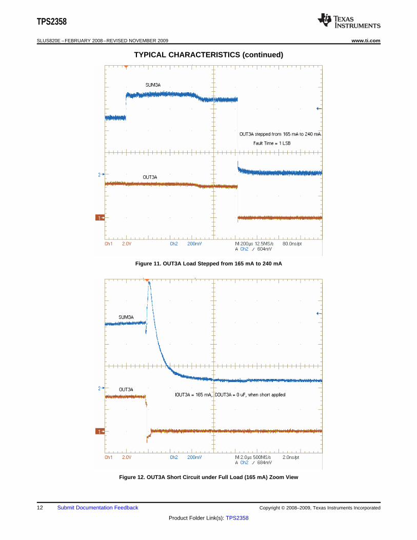
TYPICAL CHARACTERISTICS (continued)
Figure 11. OUT3A Load Stepped from 165 mA to 240 mA
Figure 12. OUT3A Short Circuit under Full Load (165 mA) Zoom View
12 Submit Documentation Feedback Copyright © 2008–2009, Texas Instruments Incorporated
Product Folder Link(s): TPS2358

TPS2358
www.ti.com SLUS820E –FEBRUARY 2008–REVISED NOVEMBER 2009
TYPICAL CHARACTERISTICS (continued)
Figure 13. OUT3A Short Circuit Under Full Load (165 mA) Wide View
Figure 14. OUT3A Startup Into Short Circuit
Copyright © 2008–2009, Texas Instruments Incorporated Submit Documentation Feedback 13
Product Folder Link(s): TPS2358

TPS2358
SLUS820E –FEBRUARY 2008–REVISED NOVEMBER 2009 www.ti.com
TYPICAL CHARACTERISTICS (continued)
Figure 15. OUT12A Startup Into 500-Ω, 830-μF Load
Figure 16. OUT12A Startup Into 80-Watt, 830-μF Load
14 Submit Documentation Feedback Copyright © 2008–2009, Texas Instruments Incorporated
Product Folder Link(s): TPS2358

TPS2358
www.ti.com SLUS820E –FEBRUARY 2008–REVISED NOVEMBER 2009
TYPICAL CHARACTERISTICS (continued)
Figure 17. OUT12A Short Circuit Under Full Load (6.7 A) Wide View
Figure 18. OUT12A Short Circuit Under Full Load (6.7 A) Zoom View
Copyright © 2008–2009, Texas Instruments Incorporated Submit Documentation Feedback 15
Product Folder Link(s): TPS2358

TPS2358
SLUS820E –FEBRUARY 2008–REVISED NOVEMBER 2009 www.ti.com
TYPICAL CHARACTERISTICS (continued)
Figure 19. OUT12A Startup Into Short Circuit
Figure 20. OUT12A Overloaded While Supplying 6.7 A
16 Submit Documentation Feedback Copyright © 2008–2009, Texas Instruments Incorporated
Product Folder Link(s): TPS2358

TPS2358
www.ti.com SLUS820E –FEBRUARY 2008–REVISED NOVEMBER 2009
REFERENCE INFORMATION
The TPS2358 has been designed to simplify compliance with the PICMG-AMC.R2.0 and PICMG-MTCA.0specifications. These specifications were developed by the PCI Industrial Computer Manufacturers Group(PICMG). These two specifications are derivations of the PICMG-ATCA (Advanced TelecommunicationComputing Architecture) specification originally released in December, 2002.
PICMG-AMC Highlights• AMC – Advanced Mezzanine Cards• Designed to Plug Into ATCA Carrier Boards• AdvancedMC™ Focuses on Low Cost• 1 to 8 AdvancedMC™ per ATCA Carrier Board• 3.3-V Management Power (maximum current draw of 150 mA)• 12-V Payload Power – (converted to required voltages on AMC)• Maximum 80-W Dissipation per AdvancedMC™• Hotswap and Current Limiting Must be Present on Carrier Board• For Details,See www.picmg.org/v2internal/AdvancedMC.htm
PICMG-MTCA Highlights• MTCA - MicroTelecommunications Computing Architecture• Architecture for Using AMCs Without an ATCA Carrier Board• Up to 12 AMCs Per System, Plus Two MCHs and Two CUs• Focuses on Low Cost• All Functions of ATCA Carrier Board Must be Provided• MicroTCA is Also Known as MTCA, mTCA, or uTCA• For Details, See www.picmg.org/v2internal/microTCA.htm
Copyright © 2008–2009, Texas Instruments Incorporated Submit Documentation Feedback 17
Product Folder Link(s): TPS2358

TPS2358
SLUS820E –FEBRUARY 2008–REVISED NOVEMBER 2009 www.ti.com
SYSTEM OPERATION
Introduction
The TPS2358 controls two 12-V power paths and two 3.3-V power paths. Each power path can draw from asingle common supply, or from two independent supplies. The TPS2358 is in a 48-pin QFN package. Thefollowing sections describe the main functions of the TPS2358 and provide guidance for designing systemsaround this device.
Control Logic and Power-On Reset
The TPS2358's circuitry draws power from an internal bus fed by a preregulator. A capacitor attached to theVINT pin provides decoupling and output filtering for this preregulator. It can draw power from any of four inputs(IN12A, IN12B, IN3A, or IN3B) or from any of four outputs (OUT12A, OUT12B, OUT3A, or OUT3B). This featureallows the internal circuitry to function regardless of which channels receive power, or from what source. The fourexternal FET drive pins (PASSA, PASSB, BLKA, and BLKB) are held low during startup to ensure that the two12-V channels remain off. The internal 3.3-V channels are also held off. When the voltage on the internal VINTrail exceeds approximately 1 V, the power-on reset circuit initializes the TPS2358.
Enable Functions
The TPS2358 provides three external enable pins for each of its two AdvancedMC™ slots. Pulling the EN3x lowturns on the 3x channel. Pulling the EN12x pin turns on the 12x channel. If the EN12x pin goes high, theTPS2358 pulls both the PASSx and BLKx pins to ground. Pulling the ORENx pin low turns on the reverseblocking circuitry in the 12x channel. If the ORENx pin goes high, then the BLKx pin remains low. Each of the sixenable pins has an internal 200-kΩ pullup resistor to VINT. To comply with AdvancedMC™ requirements, the12-V Channels will not enable unless the associated 3.3 channel PG is asserted.
Power Good (PG) Outputs
The TPS2358 provides four active-low open-drain outputs that monitor the status of the four output voltage rails.The power good output for each channel pulls low whenever the voltage on its OUTx pin exceeds the PGthreshold. The 3.3-V channels have nominal thresholds of 2.85 V and the 12-V channels have nominalthresholds of 10.5 V.
Fault (FLT) Outputs
The TPS2358 provides four active-low, open-drain fault outputs, one for each channel. A fault output pulls lowwhen the channel has remained in current limit long enough to run out the fault timer. A channel experiencing afault condition automatically shuts down. To clear the fault and re-enable the channel, turn the channel off andback on using the appropriate ENx pin.
Current Limit and Fast Trip Thresholds
All four channels monitor current by sensing the voltage across a resistor. The 3.3-V channels use internal senseresistors with a nominal value of 290 mΩ. The 12-V channels use external sense resistors that typically lie in therange of 4 - 10 mΩ. Each channel features two distinct thresholds: a current limit threshold and a fast tripthreshold.
The current limit threshold sets the regulation point of a feedback loop. If the current flowing through the channelexceeds the current limit threshold, then this feedback loop reduces the gate-to-source voltage imposed on thepass FET. This causes the current flowing through the channel to settle to the value determined by the currentlimit threshold. For example, when a module first powers up, it draws an inrush current to charge its loadcapacitance. The current limit feedback loop ensures that this inrush current does not exceed the current limitthreshold.
The current limit feedback loop has a finite response time. Serious faults such as shorted loads require a fasterresponse in order to prevent damage to the pass FETs or voltage sags on the supply rails. A comparatormonitors the current flowing through the sense resistor, and if it ever exceeds the fast trip threshold, then itimmediately shuts off the channel. The channel turns back on slowly, allowing the current limit feedback looptime to respond. One normally sets the fast trip threshold some 2 to 5 times higher than the current limit.
18 Submit Documentation Feedback Copyright © 2008–2009, Texas Instruments Incorporated
Product Folder Link(s): TPS2358

3
650
LIMIT
SUM x
VI
R=
TPS2358
www.ti.com SLUS820E –FEBRUARY 2008–REVISED NOVEMBER 2009
3.3-V Current Limiting
The 3.3-V management power channels include internal pass FETs and current sense resistors. Theon-resistance of a management channel - including pass FET, sense resistor, metallization resistance, and bondwires - typically equals 290 mΩ and never exceeds 500 mΩ. The AdvancedMC™ specification allows a total of 1Ω between the power source and the load. The TPS2358 never consumes more than half of this budget.
3.3-V Fast Trip Function
The 3.3-V fast trip function protects the channel against short-circuit events. If the current through the channelexceeds a nominal value of 300 mA, then the TPS2358 immediately disables the internal pass transistor andthen allows it to slowly turn back on into current limiting.
3.3-V Current Limit Function
The 3.3-V current limit function internally limits the current to comply with the AdvancedMC™ and MicroTCA™specifications. External resistor RSUM3x allows the user to adjust the current limit threshold. The nominal currentlimit threshold ILIMIT equals:
(1)
A 3320-Ω resistor gives a nominal current limit of ILIMIT = 195 mA which complies with AdvancedMC™ andMicroTCA™ specifications. This resistance corresponds to an EIA 1% value. Alternatively, a 3.3-kΩ resistor willalso suffice. Whenever a 3.3-V channel enters current limit, its fault timer begins to operate (see Fault TimerProgramming section).
3.3-V Over-Temperature Shutdown
The 3.3-V over-temperature shutdown trips if a 3.3-V channel remains in current limit so long that the dietemperature exceeds approximately 140°C. When this occurs, any 3.3-V channel operating in current limit turnsoff until the chip cools by approximately 10°C. This feature prevents a prolonged fault on one 3.3-V channel fromdisabling the other 3.3-V channel, or disabling either of the 12-V channels.
Copyright © 2008–2009, Texas Instruments Incorporated Submit Documentation Feedback 19
Product Folder Link(s): TPS2358

100
FT
S
mVI
R=
12
SENSE SUM
SUMx SENSE
SET
R RV I
R
æ ö= ç ÷
è ø
0 675SET
LIMIT
SUM SENSE
RI . V
R R
æ ö= ×ç ÷
è ø
TPS2358
SLUS820E –FEBRUARY 2008–REVISED NOVEMBER 2009 www.ti.com
12-V Fast Trip and Current Limiting
Figure 21 shows a simplified block diagram of the circuitry associated with the fast trip and current limit circuitrywithin a 12-V channel. Each 12-V channel requires an external N-channel pass FET and three external resistors.These resistors allow the user to independently set the fast trip threshold and the current limit threshold, asdescribed below.
12-V Fast Trip Function
The 12-V fast trip function is designed to protect the channel against short-circuit events. If the voltage acrossRSENSE exceeds a nominal threshold of 100 mV, the device immediately disables the pass transistor anddeclares a fault condition. The nominal fast current limit equals:
(2)
12-V Current Limit Function
The 12-V current limit function regulates the PASSx pin voltage to prevent the current through the channel fromexceeding ILIMIT. The current limit circuitry includes two amplifiers, A1 and A2, as shown in Figure 21. Amplifier A1forces the voltage across external resistor RSET to equal the voltage across external resistor RSENSE. The currentthat flows through RSET also flows through external resistor RSUM, generating a voltage on the 12SUMx pin equalto:
(3)
Amplifier A2 senses the voltage on the 12SUMx pin. As long as this voltage is less than the reference voltage onits positive input (nominally 0.675 V), the amplifier sources current to PASSx. When the voltage on the 12SUMxpin exceeds the reference voltage, amplifier A2 begins to sink current from PASSx. The gate-to-source voltage ofpass FET MPASS drops until the the voltages on the two inputs of amplifier A2 balance. The current flowingthrough the channel then nominally equals:
(4)
20 Submit Documentation Feedback Copyright © 2008–2009, Texas Instruments Incorporated
Product Folder Link(s): TPS2358

0 0198LIMIT SET
I ( . A / ) R= W ×
RSENSE
RSUM
RSET
+
SETx SENMx
SUM12x
IN12x
675 mV
+
100 mV
Fast Trip
ComparatorCurrent
Limit Amp
+
30 mA
PASSx
A1
A2
SENPx
60 mA
100
1 35
10f T
. Vt C
Am=
67 4 10
-= ´ ´
T FC . T
TPS2358
www.ti.com SLUS820E –FEBRUARY 2008–REVISED NOVEMBER 2009
The recommended value of RSUM is 6810 Ω. This resistor should never equal less than 675 Ω to preventexcessive currents from flowing through the internal circuitry. Using the recommended values of RSENSE = 5 mΩand RSUM = 6810 Ω gives:
(5)
A system capable of powering an 80-Watt AdvancedMC™ module consumes a maximum of 8.25 A according toMicroTCA™ specifications. The above equation suggests RSET = 417 Ω. The nearest 1% EIA value equals 422Ω. The selection of RSET for MicroTCA™ power modules is described in the Redundant vs. Non-RedundantInrush Current Limiting section.
Figure 21. 12-V Channel Threshold Circuitry
Fault Timer Programming
The fault timers of the four channels in a TPS2358 use identical internal circuitry. Each channel requires anexternal capacitor CT connected between the CTx pin and ground. Whenever the gate drive is less than 6 V thetimer will be charging CT. When a channel goes into current limit, the TPS2358 injects 10 μA into the externalcapacitor. If the channel remains in current limit long enough for the voltage on the CTx pin to reach 1.35 V, thenthe TPS2358 shuts the channel down and pulls the FLTx pin low to declare a fault. If the channel does notremain in current limit long enough to trip the timer, then the CTx capacitor is discharged through an internal200-Ω pulldown resistor. The nominal fault time tf equals:
(6)
(7)
The user should select capacitors that provide the shortest fault times sufficient to allow down-stream loads andbulk capacitors to charge. Shorter fault times reduce the stresses imposed on the pass FETs under faultconditions. This consideration may allow the use of smaller and less expensive FETs for the 12-V channels.
Copyright © 2008–2009, Texas Instruments Incorporated Submit Documentation Feedback 21
Product Folder Link(s): TPS2358

TPS2358
Backplane
SUM3xSUM12x
RS
UM
3x
RS
UM
12x
Power Source 1
TPS2358
SUM3xSUM12x
Power Source 2
TPS2358
SUM3xSUM12x
Power Source 1
TPS2358
SUM3xSUM12x
Power Source 2
MicroTCATM Redundancy Multiswap Redundancy
Backplane
RS
UM
12x
RS
UM
3x
mC
RS
UM
3x
RS
UM
12x
mC
TPS2358
SLUS820E –FEBRUARY 2008–REVISED NOVEMBER 2009 www.ti.com
Multiswap Operation in Redundant Systems
TheTPS2358 features an additional mode of operation called Multiswap redundancy. This technique does notrequire a microcontroller, making it simpler and faster than the redundancy schemes described in theMicroTCA™ standard. Multiswap is especially attractive for AdvancedMC™ applications that require redundancybut need not comply with the MicroTCA™ power module standard.
In order to implement Multiswap redundancy, connect the SUM pins of the redundant supplies together and tie asingle RSUM resistor from this node to ground. The current limit thresholds now apply to the sum of the currentsdelivered by the redundant supplies. When implementing multiswap redundancy on 12-V channels, all of thechannels must use the same values of resistors for RSENSE and RSET.
Figure 22 compares the redundancy technique advocated by the MicroTCA™ specification to multiswapredundancy. MicroTCA™ redundancy independently limits the current delivered by each power source. Thecurrent drawn by the load cannot exceed the sum of the current limits of the individual power sources. Multiswapredundancy limits the current drawn by the load to a fixed value regardless of the number of operational powersources. Removing or inserting power sources within a multiswap system does not affect the current limit seenby the load.
Figure 22. MicroTCA™ Redundancy vs. Multiswap Redundancy
22 Submit Documentation Feedback Copyright © 2008–2009, Texas Instruments Incorporated
Product Folder Link(s): TPS2358

out src
g
dV I
dt C@
RSENSE
IN12
PASS
CR > 1k W
100 W
25 V
Gnd
10
mV
-3
mV
VG
AT
E
VOR
TPS2358
www.ti.com SLUS820E –FEBRUARY 2008–REVISED NOVEMBER 2009
12-V Inrush Slew Rate Control
As normally configured, the turn-on slew rate of the 12-V channel output voltage VOUT equals:
(8)
where ISRC equals the current sourced by the PASSx pin (nominally 30 μA) and Cg equals the effective gatecapacitance. For purposes of this computation, one can assume that the effective gate capacitanceapproximately equals the reverse transfer capacitance, CRSS. To reduce the slew rate, increase Cg by connectingadditional capacitance from PASSx to ground. Place a resistor of at least 1000 Ω in series with the additionalcapacitance to prevent it from interfering with the fast turn off of the FET. Due to the current limit function at startup it is unlikely that slew rate control will be required.
Figure 23. RC Slew Rate Control
12-V ORing Operation for Redundant Systems
The 12-V channels use external pass FETs to provide reverse blocking. The TPS2358 pulls the BLKx pin highwhen the input-to-output differential voltage VIN12x-OUT12x exceeds a nominal value of 10 mV, and it pulls thepin low when this differential falls below a nominal value of -3 mV. These thresholds provide a nominal 13 mV ofhysteresis to help prevent false triggering (Figure 24).
The source of the blocking FET connects to the source of the pass FET, and the drain of the blocking FETconnects to the load. This orients the body diode of the blocking FET such that it conducts forward current andblocks reverse current. The body diode of the blocking FET does not normally conduct current because the FETturns on when the voltage differential across it exceeds 10 mV.
Figure 24. ORing Thresholds
Copyright © 2008–2009, Texas Instruments Incorporated Submit Documentation Feedback 23
Product Folder Link(s): TPS2358

0.005 W
PG12A
EN12A
FLT12A
SENMA PASSA
4700 x 4
3.3 V
OUT3A
OUT12ASETA BLKASENPA
EN3A
GND
0.033 mF
0.033 mF
3320 WSUM3A
SUM12A
IN3AFLT3A
PG3A
EN12B
TPS2358
48 PIN QFN
OUT3B
EN3B
CT12B
VDD3B
499 W
IN12B
3.3 V
12 VIN
IN12A
IN3B
VDD3A
AGND
GND
ORENB
0.01 mFVINT
6810 W
ORENA
CT3B
CT12A
CT3A
GND
GND
OUT12B
0.01 mF0.01 mF
0.01 mF
NC
0.01 mF
AMC B
AMC A
To IPMC
and/or
LED’s
To IPMC
and/or
LED’s
From
IPMC
From
IPMC
12 V
3.3 V
12 V
3.3 V
100 W
0.033 mF
0.033 mF
0.01 mF0.01 mF
PG12B
FLT12B
4700 x 4
3.3 V
3320 WSUM3B
SUM12B
FLT3B
PG3B
6810 W
MBRM120
MBRM120
CSD16406Q3
1 mF
1 mF
0.01 mF
0.005 W
SENMB PASSBSETBSENPB
499 W
BLKB
100 W
CSD16406Q3
0.01 mF
TPS2358
SLUS820E –FEBRUARY 2008–REVISED NOVEMBER 2009 www.ti.com
Using the TPS2358 to Control Two AdvancedMC™ Slots
The TPS2358 has been designed for use on ATCA Carrier boards with a minimum number of externalcomponents. Carrier boards do not usually have redundant 3.3-V or 12-V supplies, so it is not necessary toprovide ORing functions in the power supply feeds. Consequently, the external 12-V ORing FETs have beenomitted and the BLKx pins are left unconnected.
Figure 25. Block Diagram of TPS2358 In a Non-Redundant System
24 Submit Documentation Feedback Copyright © 2008–2009, Texas Instruments Incorporated
Product Folder Link(s): TPS2358

LOAD CURRENT
PATH
LOAD CURRENT
PATH
(a) (b)
SENSE
RESISTOR
RS
ET
TPS2358
SE
NP
RS
ET
SE
NM
SE
T
TPS2358
SE
NP
SE
NM
SE
T
TPS2358
www.ti.com SLUS820E –FEBRUARY 2008–REVISED NOVEMBER 2009
Layout Considerations
TPS2358 applications require layout attention to ensure proper performance and minimize susceptibility totransients and noise. In general, all runs should be as short as possible but the list below deserves firstconsideration.1. Decoupling capacitors on IN12A, IN12B, IN3A, and IN3B should have minimal length to the pin and to GND.2. SENMx and SENPx runs must be short and run side by side to maximize common mode rejection. Kelvin
connections should be used at the points of contact with RSENSE (Figure 26).3. SETx runs need to be short on both sides of RSET.4. These runs should be as short as possible and sized to carry at least 20 Amps, more if possible.
(a) Runs on both side of RSENSE.(b) Runs from the drains and sources of the external FETs.
5. Runs from the BLK FETs to OUT12x should be as short as possible.6. Runs connecting to IN3x and OUT3x should be sized for 1 Amp or more.7. Connections to GND and SUMx pins should be minimized after the runs above have been placed.8. The device dissipates low to average power so soldering the powerpad to the board is not a requirement.
However, doing so will improve thermal performance and reduce susceptibility to noise.
Figure 26. Recommended RSENSE Layout
NOTE
Additional details omitted for clarity.
Copyright © 2008–2009, Texas Instruments Incorporated Submit Documentation Feedback 25
Product Folder Link(s): TPS2358
SPIKE NOM LOAD
LV V IC
= +
40 2 0 75
STRAIGHTWIRE
lengthL ~ . length ln - . nH
diameter
é ù´æ ö´ ´ ç ÷ê ú
è øë û
2
2
SPIKE NOM
LIC
(V V )=
-
TPS2358
SLUS820E –FEBRUARY 2008–REVISED NOVEMBER 2009 www.ti.com
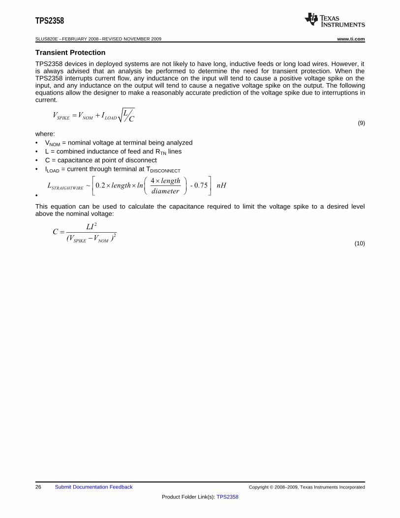
Transient Protection
TPS2358 devices in deployed systems are not likely to have long, inductive feeds or long load wires. However, itis always advised that an analysis be performed to determine the need for transient protection. When theTPS2358 interrupts current flow, any inductance on the input will tend to cause a positive voltage spike on theinput, and any inductance on the output will tend to cause a negative voltage spike on the output. The followingequations allow the designer to make a reasonably accurate prediction of the voltage spike due to interruptions incurrent.
(9)
where:• VNOM = nominal voltage at terminal being analyzed• L = combined inductance of feed and RTN lines• C = capacitance at point of disconnect• ILOAD = current through terminal at TDISCONNECT
•
This equation can be used to calculate the capacitance required to limit the voltage spike to a desired levelabove the nominal voltage:
(10)
26 Submit Documentation Feedback Copyright © 2008–2009, Texas Instruments Incorporated
Product Folder Link(s): TPS2358

AMCPOWER MODULE BACKPLANE
IN12
TPS2358
PASS BLK OUT12SENP
1 k100 100
CGS
CGD
Simplified BLK FET
CDS
CGS
CGD
Simplified PASS FET
CDS
ESD
Diode
ESD
Diode
ESD
Diode
ESD
Diode
LP
E=LI 2 /2
OUT12R
P
LP
E=LI 2/2
RP
LP
+LEMI_FILTER
LP
TPS2358
www.ti.com SLUS820E –FEBRUARY 2008–REVISED NOVEMBER 2009
Output Protection Considerations for MicroTCA Power Systems
MicroTCA Power systems have particular transient protection requirements because of the basic powerarchitecture. Traditional protection methods must be adjusted to accommodate these systems where the suppliesare OR’ed together after the inrush control and current limit circuits. However, minor changes to some standardtechniques will yield very good results.
Unlike systems which have hotswap/inrush control at the load, uTCA power modules and their hot swap circuitryare often a significant distance (up to 1 m of trace length, two way ) from the load module. Even with the bestdesigned backplanes this distance results in stray inductance which will store energy while current is beingdelivered to the load. The inductive energy can cause large negative voltage spikes at the power module outputwhen the current is switched off under load. The spikes become especially severe when the channel shuts offdue to a short circuit, which drives the current well above normal levels at shut off.
The lowest voltage allowed on the device pins is -0.3 V. If a transient makes a pin more negative than -0.3 V theinternal ESD diode attached to the pin will become forward biased and current will be conducted across thesubstrate to the ground pins. This current may disrupt normal operation or, if large enough, damage the silicon.Typical protection solutions involve capacitors, TVSs ( Transient Voltage Suppressors ) and/or a Schottky diodeto absorb the energy which appears at the power module output in the form of a large negative voltage spike.
The Risk With Output Capacitors
Putting transient filter capacitors at the output of a uTCA power module can cause nuisance trips when thatpower module is plugged into an active bus. If there is no series resistance with the capacitor and the bus is lowimpedance an inrush surge can cause the active supply to “detect” a short circuit and shut down. One possiblesolution is to put a few Ohms of resistance in series with the cap to limit inrush below the fast trip level. A bettersolution is to put a Schottky diode across the output to clamp the transient energy and shunt it to ground asshown in Figure 27. Although the Schottky diode will absorb most of the energy, the extremely fast di/dt atshutoff allows some of the leading edge energy to couple through the parasitic capacitances of the hotswap FETand the ORing FET, ( CDS, CGS, CGD ) and into the BLK and GATE pins. Protection for these pins is provided by100-Ω GATE resistors which have little effect on normal operation but provide good isolation during transientevents.
Figure 27. Figure 32 Parasitic Inductance and Transient Protection
Output Bleed Down Resistance
When the TPS2358 commands the 12-V channel off there is a small leakage current sourced by the OUT12 pin.If this leakage is ignored it can eventually charge any external capacitance to approximately 6 V. In somesystems this may be acceptable but, if not, the leakage can be bled to GND by a 1-kΩ resistor from OUT12 toGND will suffice. Maximum leakage is around 23 µA and can be modeled as a 6-V source in series with a280-kΩ resistor.
Copyright © 2008–2009, Texas Instruments Incorporated Submit Documentation Feedback 27
Product Folder Link(s): TPS2358
PACKAGE OPTION ADDENDUM
www.ti.com 10-Jun-2014
Addendum-Page 1
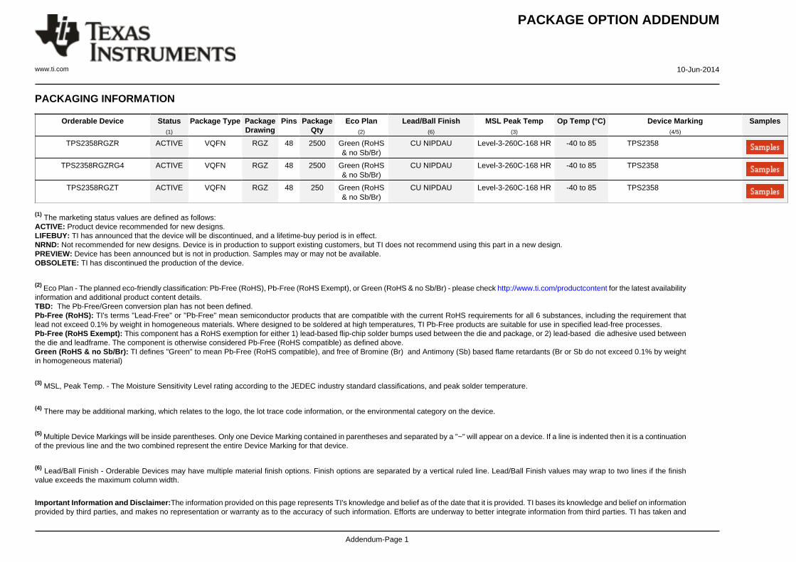
PACKAGING INFORMATION
Orderable Device Status(1)
Package Type PackageDrawing
Pins PackageQty
Eco Plan(2)
Lead/Ball Finish(6)
MSL Peak Temp(3)
Op Temp (°C) Device Marking(4/5)
Samples
TPS2358RGZR ACTIVE VQFN RGZ 48 2500 Green (RoHS& no Sb/Br)
CU NIPDAU Level-3-260C-168 HR -40 to 85 TPS2358
TPS2358RGZRG4 ACTIVE VQFN RGZ 48 2500 Green (RoHS& no Sb/Br)
CU NIPDAU Level-3-260C-168 HR -40 to 85 TPS2358
TPS2358RGZT ACTIVE VQFN RGZ 48 250 Green (RoHS& no Sb/Br)
CU NIPDAU Level-3-260C-168 HR -40 to 85 TPS2358
(1) The marketing status values are defined as follows:ACTIVE: Product device recommended for new designs.LIFEBUY: TI has announced that the device will be discontinued, and a lifetime-buy period is in effect.NRND: Not recommended for new designs. Device is in production to support existing customers, but TI does not recommend using this part in a new design.PREVIEW: Device has been announced but is not in production. Samples may or may not be available.OBSOLETE: TI has discontinued the production of the device.
(2) Eco Plan - The planned eco-friendly classification: Pb-Free (RoHS), Pb-Free (RoHS Exempt), or Green (RoHS & no Sb/Br) - please check http://www.ti.com/productcontent for the latest availabilityinformation and additional product content details.TBD: The Pb-Free/Green conversion plan has not been defined.Pb-Free (RoHS): TI's terms "Lead-Free" or "Pb-Free" mean semiconductor products that are compatible with the current RoHS requirements for all 6 substances, including the requirement thatlead not exceed 0.1% by weight in homogeneous materials. Where designed to be soldered at high temperatures, TI Pb-Free products are suitable for use in specified lead-free processes.Pb-Free (RoHS Exempt): This component has a RoHS exemption for either 1) lead-based flip-chip solder bumps used between the die and package, or 2) lead-based die adhesive used betweenthe die and leadframe. The component is otherwise considered Pb-Free (RoHS compatible) as defined above.Green (RoHS & no Sb/Br): TI defines "Green" to mean Pb-Free (RoHS compatible), and free of Bromine (Br) and Antimony (Sb) based flame retardants (Br or Sb do not exceed 0.1% by weightin homogeneous material)
(3) MSL, Peak Temp. - The Moisture Sensitivity Level rating according to the JEDEC industry standard classifications, and peak solder temperature.
(4) There may be additional marking, which relates to the logo, the lot trace code information, or the environmental category on the device.
(5) Multiple Device Markings will be inside parentheses. Only one Device Marking contained in parentheses and separated by a "~" will appear on a device. If a line is indented then it is a continuationof the previous line and the two combined represent the entire Device Marking for that device.
(6) Lead/Ball Finish - Orderable Devices may have multiple material finish options. Finish options are separated by a vertical ruled line. Lead/Ball Finish values may wrap to two lines if the finishvalue exceeds the maximum column width.
Important Information and Disclaimer:The information provided on this page represents TI's knowledge and belief as of the date that it is provided. TI bases its knowledge and belief on informationprovided by third parties, and makes no representation or warranty as to the accuracy of such information. Efforts are underway to better integrate information from third parties. TI has taken and

PACKAGE OPTION ADDENDUM
www.ti.com 10-Jun-2014
Addendum-Page 2
continues to take reasonable steps to provide representative and accurate information but may not have conducted destructive testing or chemical analysis on incoming materials and chemicals.TI and TI suppliers consider certain information to be proprietary, and thus CAS numbers and other limited information may not be available for release.
In no event shall TI's liability arising out of such information exceed the total purchase price of the TI part(s) at issue in this document sold by TI to Customer on an annual basis.

TAPE AND REEL INFORMATION
*All dimensions are nominal
Device PackageType
PackageDrawing
Pins SPQ ReelDiameter
(mm)
ReelWidth
W1 (mm)
A0(mm)
B0(mm)
K0(mm)
P1(mm)
W(mm)
Pin1Quadrant
TPS2358RGZR VQFN RGZ 48 2500 330.0 16.4 7.3 7.3 1.5 12.0 16.0 Q2
TPS2358RGZT VQFN RGZ 48 250 180.0 16.4 7.3 7.3 1.5 12.0 16.0 Q2
PACKAGE MATERIALS INFORMATION
www.ti.com 18-Dec-2015
Pack Materials-Page 1

*All dimensions are nominal
Device Package Type Package Drawing Pins SPQ Length (mm) Width (mm) Height (mm)
TPS2358RGZR VQFN RGZ 48 2500 367.0 367.0 38.0
TPS2358RGZT VQFN RGZ 48 250 210.0 185.0 35.0
PACKAGE MATERIALS INFORMATION
www.ti.com 18-Dec-2015
Pack Materials-Page 2


IMPORTANT NOTICE
Texas Instruments Incorporated and its subsidiaries (TI) reserve the right to make corrections, enhancements, improvements and otherchanges to its semiconductor products and services per JESD46, latest issue, and to discontinue any product or service per JESD48, latestissue. Buyers should obtain the latest relevant information before placing orders and should verify that such information is current andcomplete. All semiconductor products (also referred to herein as “components”) are sold subject to TI’s terms and conditions of salesupplied at the time of order acknowledgment.TI warrants performance of its components to the specifications applicable at the time of sale, in accordance with the warranty in TI’s termsand conditions of sale of semiconductor products. Testing and other quality control techniques are used to the extent TI deems necessaryto support this warranty. Except where mandated by applicable law, testing of all parameters of each component is not necessarilyperformed.TI assumes no liability for applications assistance or the design of Buyers’ products. Buyers are responsible for their products andapplications using TI components. To minimize the risks associated with Buyers’ products and applications, Buyers should provideadequate design and operating safeguards.TI does not warrant or represent that any license, either express or implied, is granted under any patent right, copyright, mask work right, orother intellectual property right relating to any combination, machine, or process in which TI components or services are used. Informationpublished by TI regarding third-party products or services does not constitute a license to use such products or services or a warranty orendorsement thereof. Use of such information may require a license from a third party under the patents or other intellectual property of thethird party, or a license from TI under the patents or other intellectual property of TI.Reproduction of significant portions of TI information in TI data books or data sheets is permissible only if reproduction is without alterationand is accompanied by all associated warranties, conditions, limitations, and notices. TI is not responsible or liable for such altereddocumentation. Information of third parties may be subject to additional restrictions.Resale of TI components or services with statements different from or beyond the parameters stated by TI for that component or servicevoids all express and any implied warranties for the associated TI component or service and is an unfair and deceptive business practice.TI is not responsible or liable for any such statements.Buyer acknowledges and agrees that it is solely responsible for compliance with all legal, regulatory and safety-related requirementsconcerning its products, and any use of TI components in its applications, notwithstanding any applications-related information or supportthat may be provided by TI. Buyer represents and agrees that it has all the necessary expertise to create and implement safeguards whichanticipate dangerous consequences of failures, monitor failures and their consequences, lessen the likelihood of failures that might causeharm and take appropriate remedial actions. Buyer will fully indemnify TI and its representatives against any damages arising out of the useof any TI components in safety-critical applications.In some cases, TI components may be promoted specifically to facilitate safety-related applications. With such components, TI’s goal is tohelp enable customers to design and create their own end-product solutions that meet applicable functional safety standards andrequirements. Nonetheless, such components are subject to these terms.No TI components are authorized for use in FDA Class III (or similar life-critical medical equipment) unless authorized officers of the partieshave executed a special agreement specifically governing such use.Only those TI components which TI has specifically designated as military grade or “enhanced plastic” are designed and intended for use inmilitary/aerospace applications or environments. Buyer acknowledges and agrees that any military or aerospace use of TI componentswhich have not been so designated is solely at the Buyer's risk, and that Buyer is solely responsible for compliance with all legal andregulatory requirements in connection with such use.TI has specifically designated certain components as meeting ISO/TS16949 requirements, mainly for automotive use. In any case of use ofnon-designated products, TI will not be responsible for any failure to meet ISO/TS16949.
Products ApplicationsAudio www.ti.com/audio Automotive and Transportation www.ti.com/automotiveAmplifiers amplifier.ti.com Communications and Telecom www.ti.com/communicationsData Converters dataconverter.ti.com Computers and Peripherals www.ti.com/computersDLP® Products www.dlp.com Consumer Electronics www.ti.com/consumer-appsDSP dsp.ti.com Energy and Lighting www.ti.com/energyClocks and Timers www.ti.com/clocks Industrial www.ti.com/industrialInterface interface.ti.com Medical www.ti.com/medicalLogic logic.ti.com Security www.ti.com/securityPower Mgmt power.ti.com Space, Avionics and Defense www.ti.com/space-avionics-defenseMicrocontrollers microcontroller.ti.com Video and Imaging www.ti.com/videoRFID www.ti-rfid.comOMAP Applications Processors www.ti.com/omap TI E2E Community e2e.ti.comWireless Connectivity www.ti.com/wirelessconnectivity
Mailing Address: Texas Instruments, Post Office Box 655303, Dallas, Texas 75265Copyright © 2015, Texas Instruments Incorporated