tpd2e007 2-channel esd protection array … · 1 2 3 gnd tpd2e007 rs232 connector rs232 transceiver...
TRANSCRIPT

1 2
3
GND
TPD2E007
RS
232
Tra
nsce
iver
RS
232
Con
nect
or
TXd
RXd
GND
IO1 IO2
GND
Product
Folder
Sample &Buy
Technical
Documents
Tools &
Software
Support &Community
An IMPORTANT NOTICE at the end of this data sheet addresses availability, warranty, changes, use in safety-critical applications,intellectual property matters and other important disclaimers. PRODUCTION DATA.
TPD2E007SLVS796I –SEPTEMBER 2008–REVISED MARCH 2016
TPD2E007 2-Channel ESD Protection Array for AC-Coupled/Negative-Rail Data Interfaces
1
1 Features1• IEC 61000-4-2 Level 4 ESD Protection
– ±8-kV IEC 61000-4-2 Contact Discharge– ±15-kV IEC 61000-4-2 Air-Gap Discharge
• IEC 61000-4-5 Surge Protection– 4.5-A Peak Pulse Current (8/20-µs Pulse)
• IO Capacitance 15 pF (Max)• Low 50-nA Leakage Current• Space-Saving PicoStar™ and SOT Package
2 Applications• Cell Phones• Audio Interface Connections• Consumer Electronics (DVR, Set-Top Box, TV)• Industrial Interfaces (RS-232, RS-485, RS-422,
LVDS)
3 DescriptionThis device is a transient voltage suppressor (TVS)based electrostatic discharge (ESD) protection devicedesigned to offer system level ESD solutions for widerange of portable and industrial applications. Theback-to-back diode array allows AC-coupled ornegative-going data transmission (audio interface,LVDS, RS-485, RS-232, and so forth) withoutcompromising signal integrity. This device exceedsthe IEC 61000-4-2 (Level 4) ESD protection and isideal for providing system level ESD protection for theinternal ICs when placed near the connector.
The TPD2E007 is offered in a 4-bump PicoStar and3-pin SOT (DGK) packages. The PicoStar package(YFM), with only 0.15 mm (Max) package height, isrecommended for ultra space saving applicationwhere the package height is a key concern. ThePicoStar package can be used in either embeddedPCB board applications or in surface mountapplications. The industry standard SOT packageoffers straightforward board layout option in legacydesigns.
Device Information(1)
PART NUMBER PACKAGE BODY SIZE (NOM)
TPD2E007SOT (3) 2.00 mm x 1.25 mmPicoStar (4) 0.77 mm x 0.77 mm
(1) For all available packages, see the orderable addendum atthe end of the data sheet.
Example Schematic Equivalent Schematic Representation
2
TPD2E007SLVS796I –SEPTEMBER 2008–REVISED MARCH 2016 www.ti.com
Product Folder Links: TPD2E007
Submit Documentation Feedback Copyright © 2008–2016, Texas Instruments Incorporated
Table of Contents1 Features .................................................................. 12 Applications ........................................................... 13 Description ............................................................. 14 Revision History..................................................... 25 Pin Configuration and Functions ......................... 36 Specifications......................................................... 4
6.1 Absolute Maximum Ratings ...................................... 46.2 ESD Ratings.............................................................. 46.3 ESD Ratings: Surge Protection................................. 46.4 Recommended Operating Conditions....................... 46.5 Thermal Information .................................................. 46.6 Electrical Characteristics........................................... 56.7 Typical Characteristics .............................................. 5
7 Detailed Description .............................................. 67.1 Overview ................................................................... 67.2 Functional Block Diagram ......................................... 6
7.3 Feature Description................................................... 67.4 Device Functional Modes.......................................... 6
8 Application and Implementation .......................... 78.1 Application Information.............................................. 78.2 Typical Application ................................................... 7
9 Power Supply Recommendations ........................ 810 Layout..................................................................... 8
10.1 Layout Guidelines ................................................... 810.2 Layout Example ...................................................... 8
11 Device and Documentation Support ................... 911.1 Community Resources............................................ 911.2 Trademarks ............................................................. 911.3 Electrostatic Discharge Caution.............................. 911.4 Glossary .................................................................. 9
12 Mechanical, Packaging, and OrderableInformation ............................................................. 9
4 Revision HistoryNOTE: Page numbers for previous revisions may differ from page numbers in the current version.
Changes from Revision H (January 2016) to Revision I Page
• Made changes to ESDS section ............................................................................................................................................ 1
Changes from Revision G (December 2015) to Revision H Page
• Updated the break-down voltage for clarity ........................................................................................................................... 5
Changes from Revision F (August 2014) to Revision G Page
• Updated the Handling Ratings table to an ESD Ratings table and moved Tstg to the Absolute Maximum Ratingstable ....................................................................................................................................................................................... 4
• Added ƒ = 10 MHz to the Channel input capacitance test condition in the Electrical Characteristics table ......................... 5• Added Community Resources ............................................................................................................................................... 9
Changes from Revision E (August 2010) to Revision F Page
• Added Pin Configuration and Functions section, Handling Rating table, Feature Description section, DeviceFunctional Modes, Application and Implementation section, Power Supply Recommendations section, Layoutsection, Device and Documentation Support section, and Mechanical, Packaging, and Orderable Informationsection ................................................................................................................................................................................... 1
Changes from Revision D (October 2009) to Revision E Page
• Added max continuous power dissipation value for DCK package........................................................................................ 4
A1
B1
A2
B2GND
IO1 IO2
GND
IO1 1
IO2 2
3 GND
3
TPD2E007www.ti.com SLVS796I –SEPTEMBER 2008–REVISED MARCH 2016
Product Folder Links: TPD2E007
Submit Documentation FeedbackCopyright © 2008–2016, Texas Instruments Incorporated
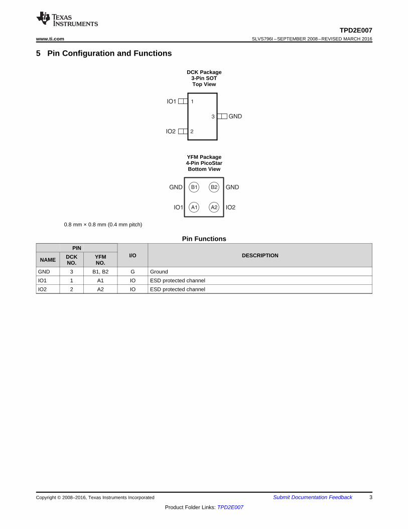
5 Pin Configuration and Functions
DCK Package3-Pin SOTTop View
YFM Package4-Pin PicoStarBottom View
0.8 mm × 0.8 mm (0.4 mm pitch)
Pin FunctionsPIN
I/O DESCRIPTIONNAME DCK
NO.YFMNO.
GND 3 B1, B2 G GroundIO1 1 A1 IO ESD protected channelIO2 2 A2 IO ESD protected channel

4
TPD2E007SLVS796I –SEPTEMBER 2008–REVISED MARCH 2016 www.ti.com
Product Folder Links: TPD2E007
Submit Documentation Feedback Copyright © 2008–2016, Texas Instruments Incorporated
(1) Stresses beyond those listed under Absolute Maximum Ratings may cause permanent damage to the device. These are stress ratingsonly, and functional operation of the device at these or any other conditions beyond those indicated in the operational sections of thespecifications is not implied. Exposure to absolute maximum-rated conditions for extended periods may affect device reliability.
6 Specifications
6.1 Absolute Maximum Ratingsover operating free-air temperature range (unless otherwise noted) (1)
MIN MAX UNITVIO –13.5 13.5 V
Continuous power dissipation(TA = 70°C)
YFM package 270mW
DCK package 218Operating temperature –40 85 °C
TJ Junction temperature 150 °C
Bump temperature (soldering)Infrared (15 s) 220
°CVapor phase (60 s) 215
Lead temperature (soldering, 10 s) 300 °CTstg Storage temperature –65 150 °C
(1) JEDEC document JEP155 states that 500-V HBM allows safe manufacturing with a standard ESD control process.(2) JEDEC document JEP157 states that 250-V CDM allows safe manufacturing with a standard ESD control process.
6.2 ESD RatingsVALUE UNIT
V(ESD)Electrostaticdischarge
Human body model (HBM), per ANSI/ESDA/JEDEC JS-001, all pins (1) ±15000V
Charged device model (CDM), per JEDEC specification JESD22-C101, all pins (2) ±1500
6.3 ESD Ratings: Surge ProtectionVALUE UNIT
V(ESD)Electrostaticdischarge IEC 61000-4-2 ESD ratings
Contact ±8000V
Air gap ±15000
6.4 Recommended Operating Conditionsover operating free-air temperature range (unless otherwise noted)
MIN NOM MAX UNITVIO Operating voltage –13 13 V
Operating temperature –40 85 °C
(1) For more information about traditional and new thermal metrics, see the Semiconductor and IC Package Thermal Metrics applicationreport, SPRA953.
6.5 Thermal Information
THERMAL METRIC (1)TPD2E007
UNITDCK (SOT) YFM (PicoStar)3 PINS 4 PINS
RθJA Junction-to-ambient thermal resistance 251.9 175.9 °C/WRθJC(top) Junction-to-case (top) thermal resistance 115.4 39.2 °C/WRθJB Junction-to-board thermal resistance 42.4 28.7 °C/WψJT Junction-to-top characterization parameter 9.4 8.3 °C/WψJB Junction-to-board characterization parameter 42.2 28.7 °C/WRθJC(bot) Junction-to-case (bottom) thermal resistance N/A N/A °C/W

1.0E-12
2.0E-12
3.0E-12
4.0E-12
5.0E-12
6.0E-12
7.0E-12
8.0E-12
9.0E-12
1.0E-11
1.1E-11
1.2E-11
1.3E-11
1.4E-11
1.5E-11
0.0 0.5 1.0 1.5 2.0 2.5 3.0 3.5 4.0 4.5 5.0
Device 2
Device 1
Input Voltage (V)
Cap
acit
an
ce (
F)
–1.50E-01
–1.25E-01
–1.00E-01
–7.50E-02
–5.00E-02
–2.50E-02
0.00E+00
2.50E-02
5.00E-02
7.50E-02
1.00E-01
1.25E-01
1.50E-01
–20.0
–17.5
–15.0
–12.5
–10.0
–7.5
–5.0
-2.5
0.0
2.5
5.0
7.5
10.0
12.5
15.0
17.5
20.0
Volts
Am
ps
Device 2
Device 1
–40
0
40
80
120
160
200
240
280
0 20 40 60 80 100 120 140 160 180 200
Time (ns)
Am
plitu
de (
V)
Time (ns)
Am
pli
tud
e (
V)
–280
–260
–240
–220
–200
–180
–160
–140
–120
–100
–80
–60
–40
–20
0
20
40
0 20 40 60 80 100 120 140 160 180 200
5
TPD2E007www.ti.com SLVS796I –SEPTEMBER 2008–REVISED MARCH 2016
Product Folder Links: TPD2E007
Submit Documentation FeedbackCopyright © 2008–2016, Texas Instruments Incorporated
(1) Typical values are at VCC = 5 V and TA = 25°C.
6.6 Electrical CharacteristicsTA = –40°C to 85°C (unless otherwise noted)
PARAMETER TEST CONDITIONS MIN TYP (1) MAX UNITVBRF Break-down voltage, pin 1 or 2 to GND IIO = 10 mA 14 VVBRR Break-down voltage, GND to pin 1 or 2 IIO = 10 mA 14 VIIO Channel leakage current 20 50 nARd Dynamic resistance 3.5 ΩCIN Channel input capacitance VIO = 2.5 V; ƒ = 10 MHz 10 15 pF
6.7 Typical CharacteristicsIEC Clamping Waveforms (20 ns/div)
Figure 1. 8-kV Contact Figure 2. –8-kV Contact
Figure 3. Capacitance vs Input Voltage at TA = 27°C Figure 4. Diode Breakdown Voltage Data at TA = 27°C

IO1 IO2
GND
6
TPD2E007SLVS796I –SEPTEMBER 2008–REVISED MARCH 2016 www.ti.com
Product Folder Links: TPD2E007
Submit Documentation Feedback Copyright © 2008–2016, Texas Instruments Incorporated
7 Detailed Description
7.1 OverviewThe TPD2E007 an ESD protection device designed to offer system level ESD solutions for wide range ofportable and industrial applications. The back-to-back diode array allows AC-coupled or negative-going datatransmission (audio interface, LVDS, RS-485, RS-232, etc.) without compromising signal integrity. The PicoStarpackage is intended to be embedded inside the printed circuit board which saves board space in portableapplications. This device exceeds the IEC 61000-4-2 (Level 4) ESD protection and is ideal for providing systemlevel ESD protection for the internal ICs when placed near the connector.
7.2 Functional Block Diagram
Figure 5. Equivalent Schematic Representation
7.3 Feature DescriptionThe TPD2E007 an ESD protection device designed to offer system level ESD solutions for wide range ofportable and industrial applications. The back-to-back diode array allows AC-coupled or negative-going datatransmission (audio interface, LVDS, RS-485, RS-232, etc.) without compromising signal integrity. The PicoStarpackage is intended to be embedded inside the printed circuit board which saves board space in portableapplications. This device exceeds the IEC 61000-4-2 (Level 4) ESD protection and is ideal for providing systemlevel ESD protection for the internal ICs when placed near the connector.
7.3.1 IEC 61000-4-2 Level 4 ESD ProtectionThe I/O pins can withstand ESD events up to ±12-kV contact and ±15 kV-air. An ESD/surge clamp diverts thecurrent to ground.
7.3.2 IEC 61000-4-5 Surge ProtectionThe I/O pins can withstand surge events up to 4.5 A (8/20 µs waveform). An ESD/surge clamp diverts thiscurrent to ground.
7.3.3 IO CapacitanceThe capacitance between each I/O pin to ground is 15 pF.
7.3.4 Low 50-nA Leakage CurrentThe I/O pins feature a low 50-nA (max) leakage current.
7.3.5 Space-Saving PicoStar and SOT PackageThis device is offered in both a space-saving PicoStar package, as well as a standard DCK package.
7.4 Device Functional ModesTPD2E007 is a passive integrated circuit that triggers when voltages are above or below VBR. During ESDevents, voltages as high as ±15 kV (air) can be directed to ground via the internal diode network. Once thevoltages on the protected line fall below the trigger levels of TPD2E007 (usually within 10’s of nano-seconds) thedevice reverts to passive.
1 2
3
GND
TPD2E007
RS
232
Tra
nsce
iver
RS
232
Con
nect
or
TXd
RXd
GND
7
TPD2E007www.ti.com SLVS796I –SEPTEMBER 2008–REVISED MARCH 2016
Product Folder Links: TPD2E007
Submit Documentation FeedbackCopyright © 2008–2016, Texas Instruments Incorporated
8 Application and Implementation
NOTEInformation in the following applications sections is not part of the TI componentspecification, and TI does not warrant its accuracy or completeness. TI’s customers areresponsible for determining suitability of components for their purposes. Customers shouldvalidate and test their design implementation to confirm system functionality.
8.1 Application InformationTPD2E007 is a diode type TVS which is typically used to provide a path to ground for dissipating ESD events onsignal lines between a human interface connector and a system. As the current from ESD passes through theTVS, only a small voltage drop is present across the diode. This is the voltage presented to the protected IC.
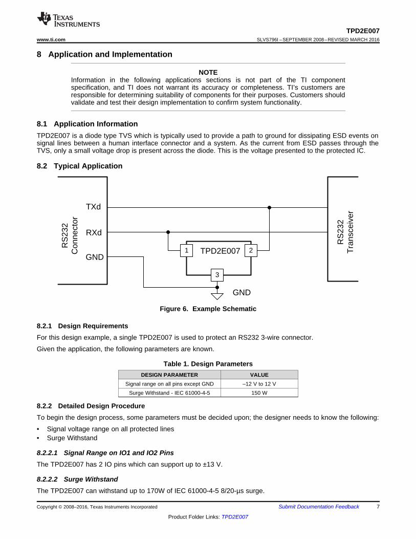
8.2 Typical Application
Figure 6. Example Schematic
8.2.1 Design RequirementsFor this design example, a single TPD2E007 is used to protect an RS232 3-wire connector.
Given the application, the following parameters are known.
Table 1. Design ParametersDESIGN PARAMETER VALUE
Signal range on all pins except GND –12 V to 12 VSurge Withstand - IEC 61000-4-5 150 W
8.2.2 Detailed Design ProcedureTo begin the design process, some parameters must be decided upon; the designer needs to know the following:
• Signal voltage range on all protected lines• Surge Withstand
8.2.2.1 Signal Range on IO1 and IO2 PinsThe TPD2E007 has 2 IO pins which can support up to ±13 V.
8.2.2.2 Surge WithstandThe TPD2E007 can withstand up to 170W of IEC 61000-4-5 8/20-µs surge.
GND
= VIA to GND
IO2
IO1
0
20
40
60
80
100
120
140
160
180
0
1
2
3
4
5
0 10 20 30 40 50
Po
wer
(W
)
Cur
rent
(A
)
Time (µs)
Current (A)
Power (W)
C014
8
TPD2E007SLVS796I –SEPTEMBER 2008–REVISED MARCH 2016 www.ti.com
Product Folder Links: TPD2E007
Submit Documentation Feedback Copyright © 2008–2016, Texas Instruments Incorporated
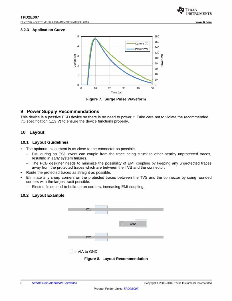
8.2.3 Application Curve
Figure 7. Surge Pulse Waveform
9 Power Supply RecommendationsThis device is a passive ESD device so there is no need to power it. Take care not to violate the recommendedI/O specification (±13 V) to ensure the device functions properly.
10 Layout
10.1 Layout Guidelines• The optimum placement is as close to the connector as possible.
– EMI during an ESD event can couple from the trace being struck to other nearby unprotected traces,resulting in early system failures.
– The PCB designer needs to minimize the possibility of EMI coupling by keeping any unprotected tracesaway from the protected traces which are between the TVS and the connector.
• Route the protected traces as straight as possible.• Eliminate any sharp corners on the protected traces between the TVS and the connector by using rounded
corners with the largest radii possible.– Electric fields tend to build up on corners, increasing EMI coupling.
10.2 Layout Example
Figure 8. Layout Recommendation

9
TPD2E007www.ti.com SLVS796I –SEPTEMBER 2008–REVISED MARCH 2016
Product Folder Links: TPD2E007
Submit Documentation FeedbackCopyright © 2008–2016, Texas Instruments Incorporated
11 Device and Documentation Support
11.1 Community ResourcesThe following links connect to TI community resources. Linked contents are provided "AS IS" by the respectivecontributors. They do not constitute TI specifications and do not necessarily reflect TI's views; see TI's Terms ofUse.
TI E2E™ Online Community TI's Engineer-to-Engineer (E2E) Community. Created to foster collaborationamong engineers. At e2e.ti.com, you can ask questions, share knowledge, explore ideas and helpsolve problems with fellow engineers.
Design Support TI's Design Support Quickly find helpful E2E forums along with design support tools andcontact information for technical support.
11.2 TrademarksPicoStar, E2E are trademarks of Texas Instruments.All other trademarks are the property of their respective owners.
11.3 Electrostatic Discharge CautionThis integrated circuit can be damaged by ESD. Texas Instruments recommends that all integrated circuits be handled withappropriate precautions. Failure to observe proper handling and installation procedures can cause damage.
ESD damage can range from subtle performance degradation to complete device failure. Precision integrated circuits may be moresusceptible to damage because very small parametric changes could cause the device not to meet its published specifications.
11.4 GlossarySLYZ022 — TI Glossary.
This glossary lists and explains terms, acronyms, and definitions.
12 Mechanical, Packaging, and Orderable InformationThe following pages include mechanical, packaging, and orderable information. This information is the mostcurrent data available for the designated devices. This data is subject to change without notice and revision ofthis document. For browser-based versions of this data sheet, refer to the left-hand navigation.

PACKAGE OPTION ADDENDUM
www.ti.com 15-Apr-2017
Addendum-Page 1
PACKAGING INFORMATION
Orderable Device Status(1)
Package Type PackageDrawing
Pins PackageQty
Eco Plan(2)
Lead/Ball Finish(6)
MSL Peak Temp(3)
Op Temp (°C) Device Marking(4/5)
Samples
TPD2E007DCKR ACTIVE SC70 DCK 3 3000 Green (RoHS& no Sb/Br)
CU NIPDAU Level-2-260C-1 YEAR -40 to 85 45U
TPD2E007YFMRG4 ACTIVE DSLGA YFM 4 3000 Green (RoHS& no Sb/Br)
Call TI Level-1-260C-UNLIM -40 to 85 45T
TPD2E007YFMTG4 ACTIVE DSLGA YFM 4 250 Green (RoHS& no Sb/Br)
Call TI Level-1-260C-UNLIM -40 to 85 45T
(1) The marketing status values are defined as follows:ACTIVE: Product device recommended for new designs.LIFEBUY: TI has announced that the device will be discontinued, and a lifetime-buy period is in effect.NRND: Not recommended for new designs. Device is in production to support existing customers, but TI does not recommend using this part in a new design.PREVIEW: Device has been announced but is not in production. Samples may or may not be available.OBSOLETE: TI has discontinued the production of the device.
(2) Eco Plan - The planned eco-friendly classification: Pb-Free (RoHS), Pb-Free (RoHS Exempt), or Green (RoHS & no Sb/Br) - please check http://www.ti.com/productcontent for the latest availabilityinformation and additional product content details.TBD: The Pb-Free/Green conversion plan has not been defined.Pb-Free (RoHS): TI's terms "Lead-Free" or "Pb-Free" mean semiconductor products that are compatible with the current RoHS requirements for all 6 substances, including the requirement thatlead not exceed 0.1% by weight in homogeneous materials. Where designed to be soldered at high temperatures, TI Pb-Free products are suitable for use in specified lead-free processes.Pb-Free (RoHS Exempt): This component has a RoHS exemption for either 1) lead-based flip-chip solder bumps used between the die and package, or 2) lead-based die adhesive used betweenthe die and leadframe. The component is otherwise considered Pb-Free (RoHS compatible) as defined above.Green (RoHS & no Sb/Br): TI defines "Green" to mean Pb-Free (RoHS compatible), and free of Bromine (Br) and Antimony (Sb) based flame retardants (Br or Sb do not exceed 0.1% by weightin homogeneous material)
(3) MSL, Peak Temp. - The Moisture Sensitivity Level rating according to the JEDEC industry standard classifications, and peak solder temperature.
(4) There may be additional marking, which relates to the logo, the lot trace code information, or the environmental category on the device.
(5) Multiple Device Markings will be inside parentheses. Only one Device Marking contained in parentheses and separated by a "~" will appear on a device. If a line is indented then it is a continuationof the previous line and the two combined represent the entire Device Marking for that device.
(6) Lead/Ball Finish - Orderable Devices may have multiple material finish options. Finish options are separated by a vertical ruled line. Lead/Ball Finish values may wrap to two lines if the finishvalue exceeds the maximum column width.
Important Information and Disclaimer:The information provided on this page represents TI's knowledge and belief as of the date that it is provided. TI bases its knowledge and belief on informationprovided by third parties, and makes no representation or warranty as to the accuracy of such information. Efforts are underway to better integrate information from third parties. TI has taken and

PACKAGE OPTION ADDENDUM
www.ti.com 15-Apr-2017
Addendum-Page 2
continues to take reasonable steps to provide representative and accurate information but may not have conducted destructive testing or chemical analysis on incoming materials and chemicals.TI and TI suppliers consider certain information to be proprietary, and thus CAS numbers and other limited information may not be available for release.
In no event shall TI's liability arising out of such information exceed the total purchase price of the TI part(s) at issue in this document sold by TI to Customer on an annual basis.

TAPE AND REEL INFORMATION
*All dimensions are nominal
Device PackageType
PackageDrawing
Pins SPQ ReelDiameter
(mm)
ReelWidth
W1 (mm)
A0(mm)
B0(mm)
K0(mm)
P1(mm)
W(mm)
Pin1Quadrant
TPD2E007DCKR SC70 DCK 3 3000 179.0 8.4 2.4 2.4 1.19 4.0 8.0 Q3
TPD2E007YFMRG4 DSLGA YFM 4 3000 178.0 9.2 0.83 0.83 0.19 4.0 8.0 Q1
TPD2E007YFMTG4 DSLGA YFM 4 250 178.0 9.2 0.83 0.83 0.19 4.0 8.0 Q1
PACKAGE MATERIALS INFORMATION
www.ti.com 3-Aug-2017
Pack Materials-Page 1
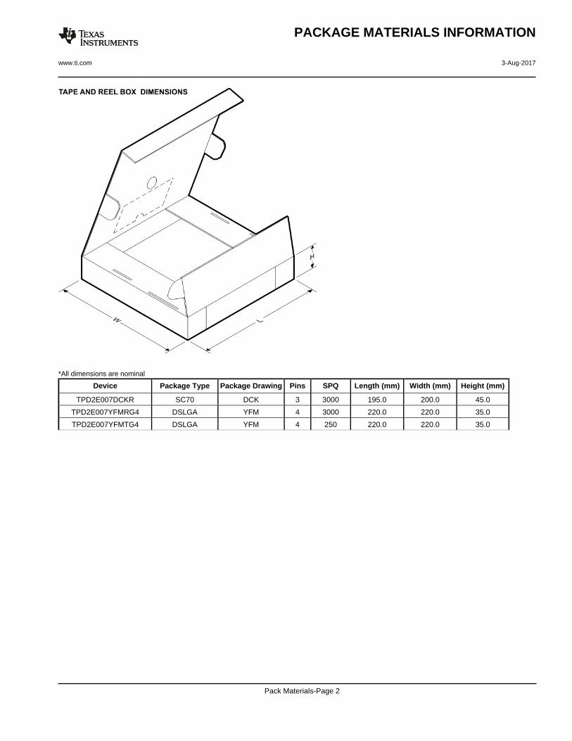
*All dimensions are nominal
Device Package Type Package Drawing Pins SPQ Length (mm) Width (mm) Height (mm)
TPD2E007DCKR SC70 DCK 3 3000 195.0 200.0 45.0
TPD2E007YFMRG4 DSLGA YFM 4 3000 220.0 220.0 35.0
TPD2E007YFMTG4 DSLGA YFM 4 250 220.0 220.0 35.0
PACKAGE MATERIALS INFORMATION
www.ti.com 3-Aug-2017
Pack Materials-Page 2

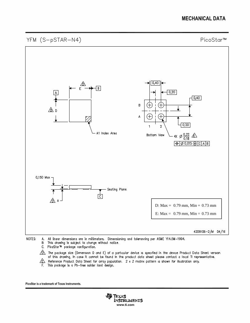
D: Max =
E: Max =
0.79 mm, Min =
0.79 mm, Min =
0.73 mm
0.73 mm

IMPORTANT NOTICE
Texas Instruments Incorporated (TI) reserves the right to make corrections, enhancements, improvements and other changes to itssemiconductor products and services per JESD46, latest issue, and to discontinue any product or service per JESD48, latest issue. Buyersshould obtain the latest relevant information before placing orders and should verify that such information is current and complete.TI’s published terms of sale for semiconductor products (http://www.ti.com/sc/docs/stdterms.htm) apply to the sale of packaged integratedcircuit products that TI has qualified and released to market. Additional terms may apply to the use or sale of other types of TI products andservices.Reproduction of significant portions of TI information in TI data sheets is permissible only if reproduction is without alteration and isaccompanied by all associated warranties, conditions, limitations, and notices. TI is not responsible or liable for such reproduceddocumentation. Information of third parties may be subject to additional restrictions. Resale of TI products or services with statementsdifferent from or beyond the parameters stated by TI for that product or service voids all express and any implied warranties for theassociated TI product or service and is an unfair and deceptive business practice. TI is not responsible or liable for any such statements.Buyers and others who are developing systems that incorporate TI products (collectively, “Designers”) understand and agree that Designersremain responsible for using their independent analysis, evaluation and judgment in designing their applications and that Designers havefull and exclusive responsibility to assure the safety of Designers' applications and compliance of their applications (and of all TI productsused in or for Designers’ applications) with all applicable regulations, laws and other applicable requirements. Designer represents that, withrespect to their applications, Designer has all the necessary expertise to create and implement safeguards that (1) anticipate dangerousconsequences of failures, (2) monitor failures and their consequences, and (3) lessen the likelihood of failures that might cause harm andtake appropriate actions. Designer agrees that prior to using or distributing any applications that include TI products, Designer willthoroughly test such applications and the functionality of such TI products as used in such applications.TI’s provision of technical, application or other design advice, quality characterization, reliability data or other services or information,including, but not limited to, reference designs and materials relating to evaluation modules, (collectively, “TI Resources”) are intended toassist designers who are developing applications that incorporate TI products; by downloading, accessing or using TI Resources in anyway, Designer (individually or, if Designer is acting on behalf of a company, Designer’s company) agrees to use any particular TI Resourcesolely for this purpose and subject to the terms of this Notice.TI’s provision of TI Resources does not expand or otherwise alter TI’s applicable published warranties or warranty disclaimers for TIproducts, and no additional obligations or liabilities arise from TI providing such TI Resources. TI reserves the right to make corrections,enhancements, improvements and other changes to its TI Resources. TI has not conducted any testing other than that specificallydescribed in the published documentation for a particular TI Resource.Designer is authorized to use, copy and modify any individual TI Resource only in connection with the development of applications thatinclude the TI product(s) identified in such TI Resource. NO OTHER LICENSE, EXPRESS OR IMPLIED, BY ESTOPPEL OR OTHERWISETO ANY OTHER TI INTELLECTUAL PROPERTY RIGHT, AND NO LICENSE TO ANY TECHNOLOGY OR INTELLECTUAL PROPERTYRIGHT OF TI OR ANY THIRD PARTY IS GRANTED HEREIN, including but not limited to any patent right, copyright, mask work right, orother intellectual property right relating to any combination, machine, or process in which TI products or services are used. Informationregarding or referencing third-party products or services does not constitute a license to use such products or services, or a warranty orendorsement thereof. Use of TI Resources may require a license from a third party under the patents or other intellectual property of thethird party, or a license from TI under the patents or other intellectual property of TI.TI RESOURCES ARE PROVIDED “AS IS” AND WITH ALL FAULTS. TI DISCLAIMS ALL OTHER WARRANTIES ORREPRESENTATIONS, EXPRESS OR IMPLIED, REGARDING RESOURCES OR USE THEREOF, INCLUDING BUT NOT LIMITED TOACCURACY OR COMPLETENESS, TITLE, ANY EPIDEMIC FAILURE WARRANTY AND ANY IMPLIED WARRANTIES OFMERCHANTABILITY, FITNESS FOR A PARTICULAR PURPOSE, AND NON-INFRINGEMENT OF ANY THIRD PARTY INTELLECTUALPROPERTY RIGHTS. TI SHALL NOT BE LIABLE FOR AND SHALL NOT DEFEND OR INDEMNIFY DESIGNER AGAINST ANY CLAIM,INCLUDING BUT NOT LIMITED TO ANY INFRINGEMENT CLAIM THAT RELATES TO OR IS BASED ON ANY COMBINATION OFPRODUCTS EVEN IF DESCRIBED IN TI RESOURCES OR OTHERWISE. IN NO EVENT SHALL TI BE LIABLE FOR ANY ACTUAL,DIRECT, SPECIAL, COLLATERAL, INDIRECT, PUNITIVE, INCIDENTAL, CONSEQUENTIAL OR EXEMPLARY DAMAGES INCONNECTION WITH OR ARISING OUT OF TI RESOURCES OR USE THEREOF, AND REGARDLESS OF WHETHER TI HAS BEENADVISED OF THE POSSIBILITY OF SUCH DAMAGES.Unless TI has explicitly designated an individual product as meeting the requirements of a particular industry standard (e.g., ISO/TS 16949and ISO 26262), TI is not responsible for any failure to meet such industry standard requirements.Where TI specifically promotes products as facilitating functional safety or as compliant with industry functional safety standards, suchproducts are intended to help enable customers to design and create their own applications that meet applicable functional safety standardsand requirements. Using products in an application does not by itself establish any safety features in the application. Designers mustensure compliance with safety-related requirements and standards applicable to their applications. Designer may not use any TI products inlife-critical medical equipment unless authorized officers of the parties have executed a special contract specifically governing such use.Life-critical medical equipment is medical equipment where failure of such equipment would cause serious bodily injury or death (e.g., lifesupport, pacemakers, defibrillators, heart pumps, neurostimulators, and implantables). Such equipment includes, without limitation, allmedical devices identified by the U.S. Food and Drug Administration as Class III devices and equivalent classifications outside the U.S.TI may expressly designate certain products as completing a particular qualification (e.g., Q100, Military Grade, or Enhanced Product).Designers agree that it has the necessary expertise to select the product with the appropriate qualification designation for their applicationsand that proper product selection is at Designers’ own risk. Designers are solely responsible for compliance with all legal and regulatoryrequirements in connection with such selection.Designer will fully indemnify TI and its representatives against any damages, costs, losses, and/or liabilities arising out of Designer’s non-compliance with the terms and provisions of this Notice.
Mailing Address: Texas Instruments, Post Office Box 655303, Dallas, Texas 75265Copyright © 2018, Texas Instruments Incorporated