town - open.uct.ac.za
TRANSCRIPT
Univers
ity of
Cap
e Town
RHINO SOFTWARE-DEFINED RADIO PROCESSING BLOCKS
A thesis submitted to the Department of Electrical Engineering,
UNIVERSITY OF CAPE TOWN, in fulfilment of the requirements for the degree of
Master of Science
at the
University of Cape Town
by
Lekhobola Joachim Tsoeunyane
Supervised by :
DOCTOR SIMON WINBERG
AND
PROFESSOR MICHAEL INGGS
c©University of Cape Town
November 30, 2015

The copyright of this thesis vests in the author. No quotation from it or information derived from it is to be published without full acknowledgement of the source. The thesis is to be used for private study or non-commercial research purposes only.
Published by the University of Cape Town (UCT) in terms of the non-exclusive license granted to UCT by the author.
Univers
ity of
Cap
e Tow
n

DeclarationI know the meaning of plagiarism and declare that all the work in this dissertation, save for that
which is properly acknowledged and referenced, is my own. It is being submitted for the degree
of Master of Science in Electrical Engineering at the University of Cape Town. This work has
not been submitted before for any other degree or examination in any other university.
Signature of Author: ............................
University of Cape Town
Cape Town
November 30, 2015
Signature Removed

ABSTRACT
This MSc project focuses on the design and implementation of a library of parameterizable,
modular and reusable Digital IP blocks designed around use in Software-Defined Radio (SDR)
applications and compatibility with the RHINO platform. The RHINO platform has common-
alities with the better known ROACH platform, but it is a significantly cut-down and lower-
cost alternative which has similarities in the interfacing and FPGA/Processor interconnects of
ROACH. The purpose of the library and design framework presented in this work aims to allevi-
ate some of the commercial, high cost and static structure concerns about IP cores provided by
FPGA manufactures and third-party IP vendors. It will also work around the lack of parameters
and bus compatibility issues often encountered when using the freely available open resources.
The RHINO hardware platform will be used for running practical applications and testing of
the blocks. The HDL library that is being constructed is targeted towards both novice and
experienced low-level HDL developers who can download and use it for free, and it will provide
them experience of using IP Cores that support open bus interfaces in order to exploit SoC
design without commercial, parameter and bus compatibility limitations. The provided modules
will be of particularly benefit to the novice developers in providing ready-made examples of
processing blocks, as well as parameterization settings for the interfacing blocks and associated
RF receiver side configuration settings; all together these examples will help new developers
establish effective ways to build their own SDR prototypes using RHINO.
The developed library of IP cores comprises the DSP blocks and I/O interface blocks. The DSP
blocks are realized with fundamental DSP algorithms which are FIR, IIR, FFT/IFFT and DDC
algorithms. These DSP blocks are accompanied by a description of how they can be integrated
into a common Open Standard Interconnection Bus, namely Wishbone. Furthermore, the I/O
interface blocks realize the interface control logic for 1 Gigabit Ethernet and 4DSP FMC150
ADC/DAC daughter board. The 1 Gigabit Ethernet interface core uses UDP protocol to enable
high speed data transfer between RHINO and external devices while FMC150 ADC/DAC pro-
vides air interface for RHINO at high sampling rates. The FM receiver is then built from the
IP blocks to demonstrate the importance and reusability of the library of IP blocks in the real
world context of SDR.
Testing of the IP blocks was incorporated into each step of the design process. Verification
followed the Xilinx ISE tools design flow where behavioral, functional, static timing and timing
i

simulations were all performed. The in-circuit verification for each IP block was also performed
to ensure that it actually works on spartan6 FPGA device of RHINO platform. The DSP blocks
were all tested successfully in clock frequency range of 312.5 kHz to 375MHz. However, the
design architecture of the DSP blocks allows them to easily adapt to clock frequencies outside
this range.
Moreover, the I/O interface blocks were also tested thoroughly and successfully. The ADC
and DAC were tested up to maximum sampling rates of 163.84MSPS and 61.44MSPS respec-
tively. The 1 Gigabit Ethernet could peak the throughput rate of 98.26MSa/s when tested on
a stream-based processing of RHINO platform. Lastly, the wideband FM receiver which in-
corporated both the Analog front-end and developed digital IP blocks was tested successfully.
Testing was performed by tuning to three local FM stations and spectra for all three stations
was plotted using baseband I/Q samples before FM demodulation and real-valued samples af-
ter FM demodulation. The message signals recovered through FM demodulation consisted of
expected spectral components of the FM station which are mono audio, pilot tone, stereo audio
and RBDS. The successfully developed library of IP blocks has proven that indeed it is useful
and relevant for use in rapid prototyping of SDR applications.

ACKNOWLEDGEMENTS
I would like to gladly express my gratitude to the following people who assisted towards suc-
cessful completion of this research project:
• Dr. Simon Winberg, my UCT supervisor, for his guidance, encouragement and provid-
ing me an excellent atmosphese for doing my research project.
• Prof. Michael Inggs, my UCT co-supervisor, for his advice, continuous support and im-
mense knowledge. If it was not for a meeting we had, it have taken me years to complete.
• Square Kilometer Array - South Africa, for financial assistance throughout this re-
search project
• UCT RRSG Group Members - I would like to thank the following colleagues in RRSG
research group who were always willing to help and give suggestions:
– Lerato Mohapi
– Dr. Van Der Byl
– Dr. Tong
– Justin Coetser
– Adrian Stevens
– Andrew Nicol
• My family - my wife ’Mathato Tsoeunyane for her unconditional love and being there
for me during good and bad times. And without my lovely daughter Puleng Tsoeunyane,
I would’nt have had courage to undertake this research project.
• Leronti Tsoeunyane - my late grandfather, he will forever remain my only role model.
He is the reason why I have made it this far. May his soul rest in peace.
• God The Almighty - It is only through my strong faith in Jesus Christ my saviour, that I
always felt protected and eternally blessed for having met the right people who gave their
all to help me complete my research project. Glory be to God in the highest.
iii

CONTENTS
Abstract
Acknowledgements iii
Contents iv
List of Figures x
List of Tables xiv
List of Abbreviations xvi
Nomenclature xix
1 Introduction 1
1.1 Background . . . . . . . . . . . . . . . . . . . . . . . . . . . . . . . . . . . . 1
1.2 Problem Description . . . . . . . . . . . . . . . . . . . . . . . . . . . . . . . 3
1.3 Focus . . . . . . . . . . . . . . . . . . . . . . . . . . . . . . . . . . . . . . . 3
1.4 Objectives . . . . . . . . . . . . . . . . . . . . . . . . . . . . . . . . . . . . . 4
1.5 Methodology Overview . . . . . . . . . . . . . . . . . . . . . . . . . . . . . . 4
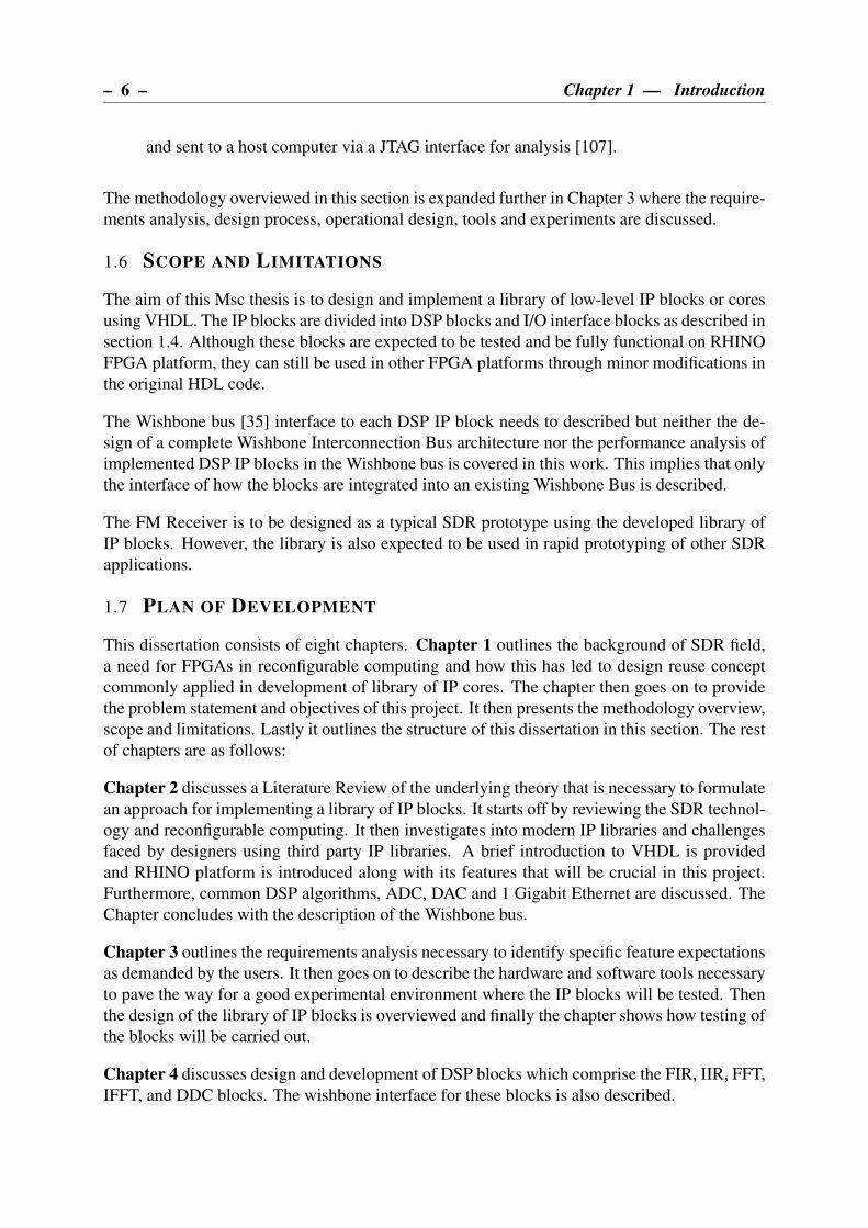
1.6 Scope and Limitations . . . . . . . . . . . . . . . . . . . . . . . . . . . . . . 6
1.7 Plan of Development . . . . . . . . . . . . . . . . . . . . . . . . . . . . . . . 6
2 Literature Review 8
2.1 The Software-Defined Radio Concept . . . . . . . . . . . . . . . . . . . . . . 8
2.2 Reconfigurable Computing . . . . . . . . . . . . . . . . . . . . . . . . . . . . 9
2.3 IP Reuse Design . . . . . . . . . . . . . . . . . . . . . . . . . . . . . . . . . . 10
2.4 IP Core Libraries . . . . . . . . . . . . . . . . . . . . . . . . . . . . . . . . . 12
2.5 VHDL . . . . . . . . . . . . . . . . . . . . . . . . . . . . . . . . . . . . . . . 12
2.6 RHINO . . . . . . . . . . . . . . . . . . . . . . . . . . . . . . . . . . . . . . 13
2.6.1 RHINO features . . . . . . . . . . . . . . . . . . . . . . . . . . . . . 13
2.6.2 RHINO Target Applications . . . . . . . . . . . . . . . . . . . . . . . 14
iv
CONTENTS – v –
2.6.3 Alternate FPGA Platforms for SDR . . . . . . . . . . . . . . . . . . . 14
2.6.3.1 ROACH . . . . . . . . . . . . . . . . . . . . . . . . . . . . 14
2.6.3.2 USRP N200 and N210 . . . . . . . . . . . . . . . . . . . . . 15
2.6.3.3 BEE4 . . . . . . . . . . . . . . . . . . . . . . . . . . . . . . 15
2.7 Digital Signal Processing Algorithms . . . . . . . . . . . . . . . . . . . . . . 15
2.7.1 Digital Filter . . . . . . . . . . . . . . . . . . . . . . . . . . . . . . . 16
2.7.1.1 FIR Filter . . . . . . . . . . . . . . . . . . . . . . . . . . . 17
2.7.1.2 IIR Filter . . . . . . . . . . . . . . . . . . . . . . . . . . . . 20
2.7.2 FFT . . . . . . . . . . . . . . . . . . . . . . . . . . . . . . . . . . . . 22
2.7.3 Digital-Down Converter . . . . . . . . . . . . . . . . . . . . . . . . . 24
2.8 Gigabit Ethernet and Networking . . . . . . . . . . . . . . . . . . . . . . . . . 25
2.9 Analog-to-digital and digital-to-analogue conversion card . . . . . . . . . . . . 27
2.10 ADC Noise Specifications . . . . . . . . . . . . . . . . . . . . . . . . . . . . 28
2.11 Frequency Modulation and Demodulation . . . . . . . . . . . . . . . . . . . . 29
2.12 Wishbone Bus . . . . . . . . . . . . . . . . . . . . . . . . . . . . . . . . . . . 31
2.13 Conclusions . . . . . . . . . . . . . . . . . . . . . . . . . . . . . . . . . . . . 32
3 Methodology 35
3.1 User Requirements for IP blocks Library . . . . . . . . . . . . . . . . . . . . . 35
3.1.1 Functional Requirements . . . . . . . . . . . . . . . . . . . . . . . . . 35
3.1.2 Non-Functional Requirements . . . . . . . . . . . . . . . . . . . . . . 36
3.2 Domain Requirements . . . . . . . . . . . . . . . . . . . . . . . . . . . . . . 36
3.3 Design Process . . . . . . . . . . . . . . . . . . . . . . . . . . . . . . . . . . 37
3.4 Operational Design . . . . . . . . . . . . . . . . . . . . . . . . . . . . . . . . 38
3.4.1 DSP blocks . . . . . . . . . . . . . . . . . . . . . . . . . . . . . . . . 39
3.4.1.1 Digital Filtering . . . . . . . . . . . . . . . . . . . . . . . . 39
3.4.1.2 Fourier Transform . . . . . . . . . . . . . . . . . . . . . . . 40
3.4.1.3 Channelization . . . . . . . . . . . . . . . . . . . . . . . . . 40
3.4.2 I/O blocks . . . . . . . . . . . . . . . . . . . . . . . . . . . . . . . . . 40
3.4.3 Digital Wideband FM receiver . . . . . . . . . . . . . . . . . . . . . . 41
3.5 Experimental Environment . . . . . . . . . . . . . . . . . . . . . . . . . . . . 41
3.5.1 Hardware . . . . . . . . . . . . . . . . . . . . . . . . . . . . . . . . . 41
3.5.2 Software Tools . . . . . . . . . . . . . . . . . . . . . . . . . . . . . . 43
3.6 Experiments . . . . . . . . . . . . . . . . . . . . . . . . . . . . . . . . . . . . 44
3.6.1 Testing DSP cores . . . . . . . . . . . . . . . . . . . . . . . . . . . . 44
3.6.2 Testing 1Gbps Ethernet interface core . . . . . . . . . . . . . . . . . . 44
3.6.3 Testing ADC . . . . . . . . . . . . . . . . . . . . . . . . . . . . . . . 44
3.6.4 Testing DAC . . . . . . . . . . . . . . . . . . . . . . . . . . . . . . . 45
3.6.5 Testing a Streaming Core . . . . . . . . . . . . . . . . . . . . . . . . . 45
3.6.6 Testing a Digital Wideband FM Receiver . . . . . . . . . . . . . . . . 46
4 Design of SDR DSP Blocks 47
– vi – CONTENTS
4.1 FIR IP core . . . . . . . . . . . . . . . . . . . . . . . . . . . . . . . . . . . . 47
4.1.1 Filter Structure . . . . . . . . . . . . . . . . . . . . . . . . . . . . . . 48
4.1.2 Filter Coefficients Generation . . . . . . . . . . . . . . . . . . . . . . 49
4.1.3 Parameters and Ports . . . . . . . . . . . . . . . . . . . . . . . . . . . 50
4.1.4 Timing Constraints . . . . . . . . . . . . . . . . . . . . . . . . . . . . 50
4.1.5 Wishbone Interface . . . . . . . . . . . . . . . . . . . . . . . . . . . . 51
4.1.6 FIR Core Test . . . . . . . . . . . . . . . . . . . . . . . . . . . . . . . 53
4.2 IIR IP Core . . . . . . . . . . . . . . . . . . . . . . . . . . . . . . . . . . . . 53
4.2.1 Filter Coefficients Generation . . . . . . . . . . . . . . . . . . . . . . 53
4.2.2 Parameters and Ports . . . . . . . . . . . . . . . . . . . . . . . . . . . 55
4.2.3 Timing Constraints . . . . . . . . . . . . . . . . . . . . . . . . . . . . 56
4.2.4 Wishbone Interface . . . . . . . . . . . . . . . . . . . . . . . . . . . . 56
4.2.5 IIR core Test . . . . . . . . . . . . . . . . . . . . . . . . . . . . . . . 57
4.3 FFT/IFFT IP Core . . . . . . . . . . . . . . . . . . . . . . . . . . . . . . . . 57
4.3.1 Design Structure . . . . . . . . . . . . . . . . . . . . . . . . . . . . . 59
4.3.1.1 Butterflies . . . . . . . . . . . . . . . . . . . . . . . . . . . 60
4.3.1.2 Shift Register . . . . . . . . . . . . . . . . . . . . . . . . . 61
4.3.1.3 Complex Multiplier . . . . . . . . . . . . . . . . . . . . . . 61
4.3.1.4 Twiddle Factor ROM . . . . . . . . . . . . . . . . . . . . . 62
4.3.1.5 Controller . . . . . . . . . . . . . . . . . . . . . . . . . . . 62
4.3.2 Parameters and Ports . . . . . . . . . . . . . . . . . . . . . . . . . . . 62
4.3.3 Core Generation Flow for Higher Length FFTs . . . . . . . . . . . . . 63
4.3.4 Timing Constraints . . . . . . . . . . . . . . . . . . . . . . . . . . . . 63
4.3.5 Wishbone Interface . . . . . . . . . . . . . . . . . . . . . . . . . . . . 65
4.3.6 FFT/IFFT core Test . . . . . . . . . . . . . . . . . . . . . . . . . . . . 66
4.4 DDC IP Core . . . . . . . . . . . . . . . . . . . . . . . . . . . . . . . . . . . 66
4.4.1 DDC structure . . . . . . . . . . . . . . . . . . . . . . . . . . . . . . 66
4.4.1.1 NCO . . . . . . . . . . . . . . . . . . . . . . . . . . . . . . 66
4.4.1.2 Digital Mixer . . . . . . . . . . . . . . . . . . . . . . . . . 68
4.4.1.3 CIC Decimation filter . . . . . . . . . . . . . . . . . . . . . 68
4.4.1.4 Compensation Filter . . . . . . . . . . . . . . . . . . . . . . 69
4.4.2 Parameter and Ports . . . . . . . . . . . . . . . . . . . . . . . . . . . 69
4.4.3 Timing Constraints . . . . . . . . . . . . . . . . . . . . . . . . . . . . 70
4.4.4 Wishbone Interface . . . . . . . . . . . . . . . . . . . . . . . . . . . . 71
4.4.5 DDC Core Test . . . . . . . . . . . . . . . . . . . . . . . . . . . . . . 73
5 Design of SDR I/O Interface Blocks 74
5.1 4DSP-FMC150 interface Core . . . . . . . . . . . . . . . . . . . . . . . . . . 74
5.1.1 CDCE72010 programming settings . . . . . . . . . . . . . . . . . . . 75
5.1.1.1 PLL configuration parameters . . . . . . . . . . . . . . . . . 75
5.1.1.2 PLL Design . . . . . . . . . . . . . . . . . . . . . . . . . . 76
5.1.2 ADS62P49 interface . . . . . . . . . . . . . . . . . . . . . . . . . . . 78
CONTENTS – vii –
5.1.2.1 Sample Rate . . . . . . . . . . . . . . . . . . . . . . . . . . 79
5.1.2.2 Bit and Word Alignment . . . . . . . . . . . . . . . . . . . . 79
5.1.3 DAC3283 interface . . . . . . . . . . . . . . . . . . . . . . . . . . . . 80
5.1.4 ADC and DAC Test . . . . . . . . . . . . . . . . . . . . . . . . . . . . 81
5.2 UDP/IP core . . . . . . . . . . . . . . . . . . . . . . . . . . . . . . . . . . . 81
5.2.1 Overall Architecture . . . . . . . . . . . . . . . . . . . . . . . . . . . 82
5.2.1.1 Physical Layer . . . . . . . . . . . . . . . . . . . . . . . . . 82
5.2.1.2 Data Link Layer . . . . . . . . . . . . . . . . . . . . . . . . 83
5.2.1.3 Network Layer . . . . . . . . . . . . . . . . . . . . . . . . . 85
5.2.1.4 Transport Layer . . . . . . . . . . . . . . . . . . . . . . . . 85
5.2.2 Structure of the UDP/IP core . . . . . . . . . . . . . . . . . . . . . . . 85
5.2.3 Marvell 88E1111S/PHY initialization . . . . . . . . . . . . . . . . . . 88
5.2.4 UDP/IP Core Interface . . . . . . . . . . . . . . . . . . . . . . . . . . 88
5.2.5 UDP/IP Core Test . . . . . . . . . . . . . . . . . . . . . . . . . . . . 89
6 Design of FM Receiver 91
6.1 Design of Digital Receiver . . . . . . . . . . . . . . . . . . . . . . . . . . . . 91
6.2 Design of Analog RF Front-end . . . . . . . . . . . . . . . . . . . . . . . . . 95
7 Results and Discussion 97
7.1 FIR Core Test . . . . . . . . . . . . . . . . . . . . . . . . . . . . . . . . . . . 97
7.2 IIR Core Test . . . . . . . . . . . . . . . . . . . . . . . . . . . . . . . . . . . 100
7.3 FFT/IFFT Core Test . . . . . . . . . . . . . . . . . . . . . . . . . . . . . . . 101
7.3.1 Testbench . . . . . . . . . . . . . . . . . . . . . . . . . . . . . . . . . 102
7.3.2 Hardware Test . . . . . . . . . . . . . . . . . . . . . . . . . . . . . . 103
7.4 DDC Core Test . . . . . . . . . . . . . . . . . . . . . . . . . . . . . . . . . . 104
7.4.1 Noise Free System Test . . . . . . . . . . . . . . . . . . . . . . . . . 106
7.4.2 Adding AWGN Noise to a Modulating Signal . . . . . . . . . . . . . . 106
7.4.3 Adding AWGN Noise to a Frequency Modulated Signal . . . . . . . . 108
7.4.4 Adding 20dB AWGN Noise to a modulating signal and frequency mod-
ulated Signal . . . . . . . . . . . . . . . . . . . . . . . . . . . . . . . 108
7.5 UDP/IP Core Test . . . . . . . . . . . . . . . . . . . . . . . . . . . . . . . . . 115
7.5.1 ARP Test . . . . . . . . . . . . . . . . . . . . . . . . . . . . . . . . . 115
7.5.2 Upstream Test . . . . . . . . . . . . . . . . . . . . . . . . . . . . . . 117
7.5.2.1 Data Transfer Test . . . . . . . . . . . . . . . . . . . . . . . 117
7.5.2.2 Transfer Speed Test . . . . . . . . . . . . . . . . . . . . . . 117
7.5.3 Downstream Test . . . . . . . . . . . . . . . . . . . . . . . . . . . . . 118
7.6 Streaming Core Test . . . . . . . . . . . . . . . . . . . . . . . . . . . . . . . 122
7.6.1 Direct Streaming . . . . . . . . . . . . . . . . . . . . . . . . . . . . . 122
7.6.2 Stream Processing With Decimation and Filtering . . . . . . . . . . . . 124
7.6.3 Testing the FFT Core inside Streaming Logic . . . . . . . . . . . . . . 128
7.7 DAC interface core Test . . . . . . . . . . . . . . . . . . . . . . . . . . . . . . 132
– viii – CONTENTS
7.8 FM Receiver Test . . . . . . . . . . . . . . . . . . . . . . . . . . . . . . . . . 132
8 Conclusions and Further Work 136
8.1 Conclusions . . . . . . . . . . . . . . . . . . . . . . . . . . . . . . . . . . . . 136
8.1.1 DSP IP blocks . . . . . . . . . . . . . . . . . . . . . . . . . . . . . . 136
8.1.2 I/O interface blocks . . . . . . . . . . . . . . . . . . . . . . . . . . . . 137
8.2 Recommendations For Further Work . . . . . . . . . . . . . . . . . . . . . . . 139
8.2.1 Upgrade the DSP blocks . . . . . . . . . . . . . . . . . . . . . . . . . 139
8.2.2 Improve the I/O interface blocks . . . . . . . . . . . . . . . . . . . . . 141
8.2.3 Refine the FM receiver . . . . . . . . . . . . . . . . . . . . . . . . . . 142
A The Attached CD 151
B FIR IP core 153
B.1 Instantiation of the FIR core . . . . . . . . . . . . . . . . . . . . . . . . . . . 153
B.2 Generating Testbench Data Files in Matlab . . . . . . . . . . . . . . . . . . . . 153
B.3 Plotting the results in Matlab . . . . . . . . . . . . . . . . . . . . . . . . . . . 154
C IIR IP core 156
C.1 Instantiation of the IIR core . . . . . . . . . . . . . . . . . . . . . . . . . . . . 156
C.2 Generating Testbench Data Files in Matlab . . . . . . . . . . . . . . . . . . . . 156
C.3 Plotting the results in Matlab . . . . . . . . . . . . . . . . . . . . . . . . . . . 158
D FFT/IFFT IP core 160
D.1 Instantiation of the FFT/IFFT core . . . . . . . . . . . . . . . . . . . . . . . . 160
D.2 Generating Testbench Data Files in Matlab . . . . . . . . . . . . . . . . . . . . 160
D.3 Plotting the results in Matlab . . . . . . . . . . . . . . . . . . . . . . . . . . . 161
D.3.1 Decimal to 2’s complement binary Conversion . . . . . . . . . . . . . 162
D.4 Generating n-bit Twiddle Factors HDL ROM . . . . . . . . . . . . . . . . . . 162
E DDC IP core 165
E.1 Instantiation of the DDC core . . . . . . . . . . . . . . . . . . . . . . . . . . . 165
E.2 Generating Testbench Data Files in Matlab . . . . . . . . . . . . . . . . . . . . 166
E.3 Generate Coefficients for a Compensation Filter . . . . . . . . . . . . . . . . 169
E.4 Plotting the results in Matlab . . . . . . . . . . . . . . . . . . . . . . . . . . . 170
F UDP/IP core 172
F.1 Instantiation of the UDP/IP core . . . . . . . . . . . . . . . . . . . . . . . . . 172
G ADC/DAC core 174
G.1 Instantiation of the ADC/DAC core for interfacing FMC150 . . . . . . . . . . 174
H Digital FM Receiver 176
H.1 Top Level Design of Digital IP Blocks . . . . . . . . . . . . . . . . . . . . . . 176

CONTENTS – ix –
H.2 FM demodulation function in Matlab [84] . . . . . . . . . . . . . . . . . . . . 185
H.3 Plotting the FPGA results in Matlab . . . . . . . . . . . . . . . . . . . . . . . 185

LIST OF FIGURES
1.1 Radio transceiver architecture . . . . . . . . . . . . . . . . . . . . . . . . . . 2
1.2 Design flow for development of IP blocks for RHINO . . . . . . . . . . . . . . 5
2.1 Ideal Software Defined Radio Architecture [63] . . . . . . . . . . . . . . . . . 9
2.2 Realistic Software Defined Radio Architecture [63] . . . . . . . . . . . . . . . 9
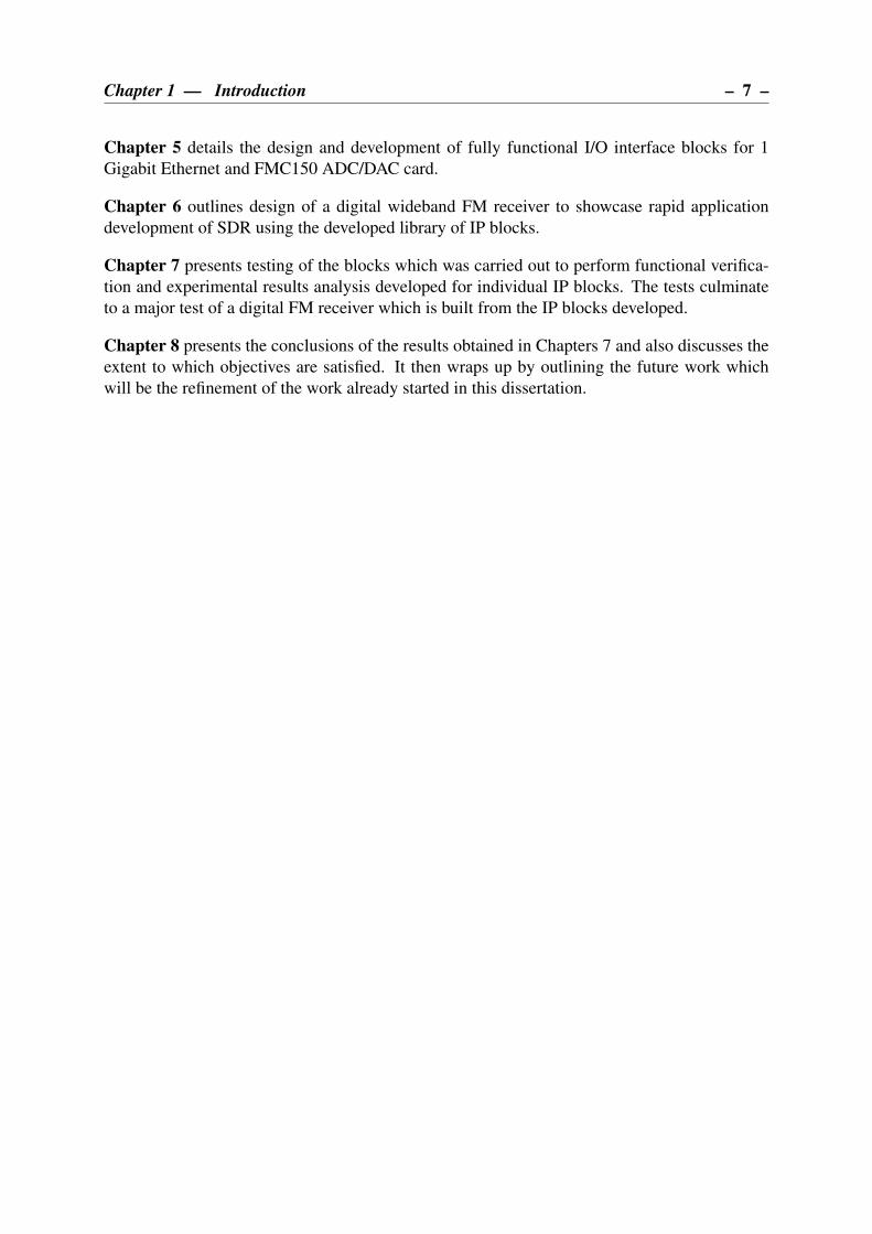
2.3 Device technologies used for reconfigurable digital systems [66] . . . . . . . . 10
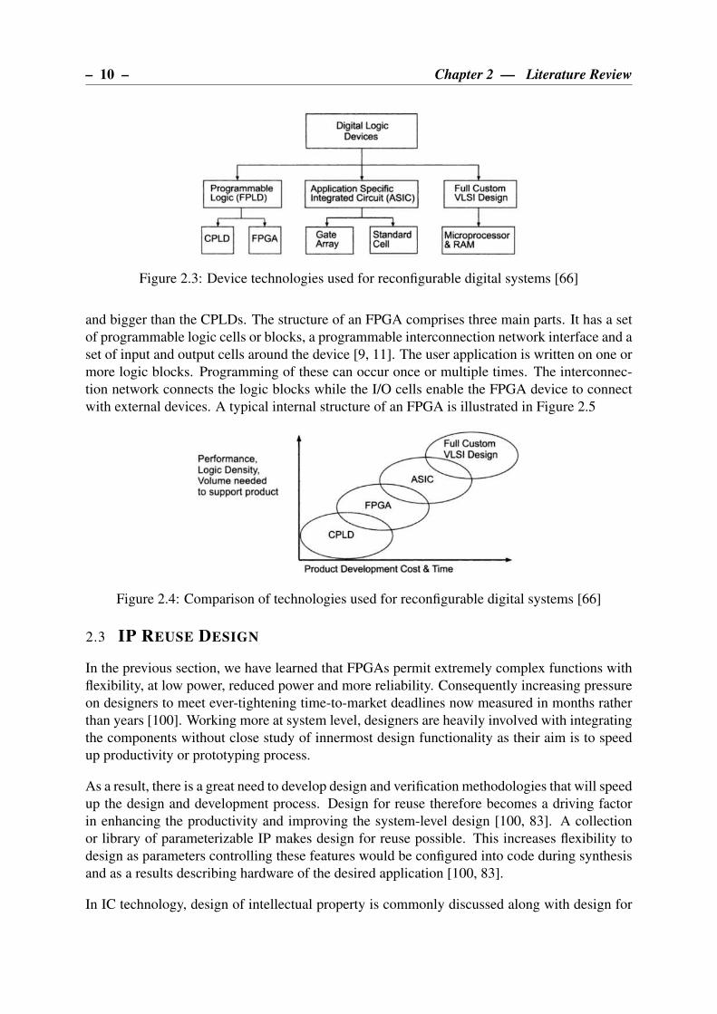
2.4 Comparison of technologies used for reconfigurable digital systems [66] . . . . 10
2.5 An internal structure of FPGA [9] . . . . . . . . . . . . . . . . . . . . . . . . 11
2.6 Essential issues for IP reuse [30] . . . . . . . . . . . . . . . . . . . . . . . . . 11
2.7 RHINO-high level block diagram [87] . . . . . . . . . . . . . . . . . . . . . . 13
2.8 Ideal linear system of direct form [11] . . . . . . . . . . . . . . . . . . . . . . 18
2.9 Transpose form FIR filter [11] . . . . . . . . . . . . . . . . . . . . . . . . . . 19
2.10 Optimised structures for linear-phase FIR filters (T = z−1: Sample period de-
lay) (i) FIR Symmetric structure when the filter order M is an odd number. (ii)
FIR Symmetric structure when the filter order M is an even number. [85] . . . 19
2.11 Moving Average FIR filter [75] . . . . . . . . . . . . . . . . . . . . . . . . . . 20
2.12 Generic structure of IIR filter [11] . . . . . . . . . . . . . . . . . . . . . . . . 21
2.13 Digital biquad filters [3] . . . . . . . . . . . . . . . . . . . . . . . . . . . . . . 22
2.14 Various architectures for pipeline FFT processor [34] . . . . . . . . . . . . . . 23
2.15 Block diagram of a DDC [49] . . . . . . . . . . . . . . . . . . . . . . . . . . 25
2.16 The OSI and generic Ethernet Physical Model [50] . . . . . . . . . . . . . . . 26
2.17 FMC150 block diagram [1] . . . . . . . . . . . . . . . . . . . . . . . . . . . . 27
2.18 Frequency spectra of frequency-modulation waves, showing effects of varying
the frequency deviation [53] . . . . . . . . . . . . . . . . . . . . . . . . . . . 31
2.19 Wishbone bus basic connection [35] . . . . . . . . . . . . . . . . . . . . . . . 32
3.1 FPGA Design Flow using Xilinx ISE [101] . . . . . . . . . . . . . . . . . . . 38
3.2 Architecture of RHINO SDR processing blocks . . . . . . . . . . . . . . . . . 38
3.3 IP core design process . . . . . . . . . . . . . . . . . . . . . . . . . . . . . . 39
3.4 A flowchart showing experimental development process . . . . . . . . . . . . . 41
3.5 Experimental setup for the DSP cores . . . . . . . . . . . . . . . . . . . . . . 44
3.6 Experimental setup for 1 Gigabit ethernet core . . . . . . . . . . . . . . . . . . 45
x
LIST OF FIGURES – xi –
3.7 A block diagram showing experimental setup for ADC interface core . . . . . . 45
3.8 A block diagram showing experimental setup for DAC interface core . . . . . . 45
3.9 Experimental setup for a Streaming core using ADC and 1 Gigabit Ethernet
interface cores . . . . . . . . . . . . . . . . . . . . . . . . . . . . . . . . . . . 46
3.10 Experimental setup for a digital wideband FM receiver . . . . . . . . . . . . . 46
4.1 A block diagram differentiating a Core and IP Core . . . . . . . . . . . . . . . 47
4.2 An overall architecture of a DSP IP Core . . . . . . . . . . . . . . . . . . . . . 48
4.3 Architecture of FIR IP Core . . . . . . . . . . . . . . . . . . . . . . . . . . . 48
4.4 Parallel FIR structures . . . . . . . . . . . . . . . . . . . . . . . . . . . . . . 49
4.5 FIR core data flow diagram . . . . . . . . . . . . . . . . . . . . . . . . . . . . 49
4.6 FIR core input/output timing waveform . . . . . . . . . . . . . . . . . . . . . 51
4.7 FIR core and Wishbone slave interface . . . . . . . . . . . . . . . . . . . . . . 52
4.8 Architecture of IIR IP Core . . . . . . . . . . . . . . . . . . . . . . . . . . . . 53
4.9 Cascaded Direct Form I Biquad IIR filter . . . . . . . . . . . . . . . . . . . . . 54
4.10 Six Cascaded second-order sections (DFI=Direct Form I) . . . . . . . . . . . . 54
4.11 IIR core input/output timing waveform . . . . . . . . . . . . . . . . . . . . . . 57
4.12 IIR core and Wishbone slave interface . . . . . . . . . . . . . . . . . . . . . . 58
4.13 The architecture of FFT IP Core . . . . . . . . . . . . . . . . . . . . . . . . . 59
4.14 32-point FFT structure using Radix-22 Single-Path Delay Feedback algorithm . 60
4.15 The single FFT pipeline stage consisting of Butterfly Type BFI and BFII and
showing how shift registers, counter, ROM and complex mulplier are connected. 61
4.16 Sign-inversion structure [81] . . . . . . . . . . . . . . . . . . . . . . . . . . . 61
4.17 A flow diagram for generation of FFT core modules for high length FFTs . . . 64
4.18 FFT/IFFT core input/output timing waveform . . . . . . . . . . . . . . . . . . 64
4.19 FFT core and Wishbone slave interface . . . . . . . . . . . . . . . . . . . . . . 65
4.20 The architecture of DDC IP Core . . . . . . . . . . . . . . . . . . . . . . . . . 67
4.21 A structure of Digital Down Converter . . . . . . . . . . . . . . . . . . . . . . 67
4.22 Block diagram of NCO core . . . . . . . . . . . . . . . . . . . . . . . . . . . 67
4.23 Block diagram of a CIC core . . . . . . . . . . . . . . . . . . . . . . . . . . . 68
4.24 DDC core input/output timing waveform . . . . . . . . . . . . . . . . . . . . . 71
4.25 DDC core and Wishbone slave interface . . . . . . . . . . . . . . . . . . . . . 72
5.1 CDCE72010 programming settings for FMC150 card . . . . . . . . . . . . . . 77
5.2 The architecture of ADS62P49 interface . . . . . . . . . . . . . . . . . . . . . 79
5.3 The architecture of DAC3283 interface . . . . . . . . . . . . . . . . . . . . . . 81
5.4 Overall architecture of UDP/IP Stack . . . . . . . . . . . . . . . . . . . . . . . 82
5.5 MAC core transmit operation [31] . . . . . . . . . . . . . . . . . . . . . . . . 83
5.6 MAC core receive operation [31] . . . . . . . . . . . . . . . . . . . . . . . . . 84
5.7 PHY Management interface . . . . . . . . . . . . . . . . . . . . . . . . . . . 84
5.8 Structure of UDP/IP Core based on a Gigabit Ethernet . . . . . . . . . . . . . 86
5.9 ARP protocol operation data flow diagram . . . . . . . . . . . . . . . . . . . . 87

– xii – LIST OF FIGURES
5.10 The structure of ARP packet . . . . . . . . . . . . . . . . . . . . . . . . . . . 87
5.11 The structure of a UDP packet . . . . . . . . . . . . . . . . . . . . . . . . . . 88
5.12 UDP Core Write operation interface . . . . . . . . . . . . . . . . . . . . . . . 90
5.13 UDP Core Read operation interface . . . . . . . . . . . . . . . . . . . . . . . 90
6.1 Digital FM receiver architecture . . . . . . . . . . . . . . . . . . . . . . . . . 92
6.2 Compensation Filter Response for 10-stage CIC-1 filter . . . . . . . . . . . . . 94
6.3 Block diagram of a Analog RF front-end . . . . . . . . . . . . . . . . . . . . . 96
7.1 Experimental environment showing Hardware and Software Tools use in this
project . . . . . . . . . . . . . . . . . . . . . . . . . . . . . . . . . . . . . . . 97
7.2 FIR core Testbench block diagram . . . . . . . . . . . . . . . . . . . . . . . . 98
7.3 The results FIR filter testbench. . . . . . . . . . . . . . . . . . . . . . . . . . . 99
7.4 IIR core Testbench block diagram . . . . . . . . . . . . . . . . . . . . . . . . 101
7.5 The results IIR filter testbench. . . . . . . . . . . . . . . . . . . . . . . . . . . 101
7.6 Testbench block diagram . . . . . . . . . . . . . . . . . . . . . . . . . . . . . 102
7.7 MATLAB and FPGA results of a 1024-point FFT and IFFT core tested with
rectangular pulse input waveform. . . . . . . . . . . . . . . . . . . . . . . . . 103
7.8 DDC core Testbench block diagram . . . . . . . . . . . . . . . . . . . . . . . 105
7.9 DDC core input vector generated in MATLAB and computed by FM modula-
tion of a 200 kHz with 94.5 MHz sampled at 122.88 MSPS. . . . . . . . . . . . 105
7.10 A 28.38MHz carrier waveform generated in MATLAB and a local oscillator
28.38MHz signal generated by NCO core in FPGA. . . . . . . . . . . . . . . . 106
7.11 Results of DDC Core and FM demodulator when a noise free input test signal
is used. . . . . . . . . . . . . . . . . . . . . . . . . . . . . . . . . . . . . . . 107
7.12 FM demodulator output showing the demodulated signal with transients and
after removing the transients. This applies to a test when a noise free input test
signal is used. . . . . . . . . . . . . . . . . . . . . . . . . . . . . . . . . . . . 108
7.13 Results of DDC Core and FM demodulator when 20dB AWGN noise is added
to a modulating signal. . . . . . . . . . . . . . . . . . . . . . . . . . . . . . . 109
7.14 FM demodulator output showing the demodulated signal with transients and
after removing the transients. This applies to a test where 20dB AWGN noise
is added to a modulating signal. . . . . . . . . . . . . . . . . . . . . . . . . . 110
7.15 Results of DDC Core and FM demodulator when 20dB AWGN noise is added
to a frequency modulated signal. . . . . . . . . . . . . . . . . . . . . . . . . . 111
7.16 FM demodulator output showing the demodulated signal with transients and
after removing the transients. This applies to a test where 20dB AWGN noise
is added to a frequency modulated input test signal. . . . . . . . . . . . . . . . 112
7.17 Results of DDC Core and FM demodulator when 20dB AWGN noise is added
to a modulating signal and frequency modulated signal. . . . . . . . . . . . . . 113
7.18 FM demodulator output showing the demodulated signal with transients and
after removing the transients. This applies to a test where 20dB AWGN noise
is added to a modulating signal and frequency modulated input test signal. . . . 114
7.19 Wireshark Capture of FPGA broadcast ARP request . . . . . . . . . . . . . . . 116

LIST OF FIGURES – xiii –
7.20 Trace of UDP traffic from FPGA showing the details of the UDP header . . . . 118
7.21 Trace of time taken for a single and 500 packets of UDP over 1Gbps Ethernet . 119
7.22 Measuring speed using Linux Speedometer Tool 2.8 . . . . . . . . . . . . . . . 120
7.23 Thoughput vs UDP Frame Length . . . . . . . . . . . . . . . . . . . . . . . . 120
7.24 Trace of UDP packets being transmitted to FGPA over 1Gbps Ethernet . . . . . 121
7.25 Capture of received UDP data on FPGA using ChipScope Pro . . . . . . . . . 121
7.26 A measured spectrum analysis for ADC input sine waveforms generated using
a function generator . . . . . . . . . . . . . . . . . . . . . . . . . . . . . . . . 122
7.27 A digitized 200kHz sine wave visualized using ChipScope Pro . . . . . . . . . 123
7.28 A digitized 200kHz visualized using ChipScope Pro . . . . . . . . . . . . . . . 124
7.29 ADC digitized signals streamed via UDP . . . . . . . . . . . . . . . . . . . . 125
7.30 20MHz tone ADC ouput streamed using UDP . . . . . . . . . . . . . . . . . . 126
7.31 FPGA results of UDP streaming when 163.84MSPS ADC is used . . . . . . . 127
7.32 Experimental setup for stream-based processing with CIC decimation filter and
Compensation Filter . . . . . . . . . . . . . . . . . . . . . . . . . . . . . . . . 127
7.33 FPGA results of UDP streaming when a CIC and FIR filters are used to process
a 200 kHz signal sampled by the ADC at 163.84 MSPS . . . . . . . . . . . . . 127
7.34 Experimental setup for FFT core as tested on the FPGA . . . . . . . . . . . . . 128
7.35 Results showing 512-point and 4096-point FFT of a 133kHz ADC wave using
MATLAB and FFT core . . . . . . . . . . . . . . . . . . . . . . . . . . . . . 129
7.36 Results showing 512-point and 4096-point FFT of a 200kHz ADC wave using
MATLAB and FFT core . . . . . . . . . . . . . . . . . . . . . . . . . . . . . 130
7.37 Results showing 512-point and 4096-point FFT of a 445kHz sine waveform
using FFT/IFFT core . . . . . . . . . . . . . . . . . . . . . . . . . . . . . . . 131
7.38 The spectra different sinusoids generated using NCO core and measured at the
FMC150 DAC output . . . . . . . . . . . . . . . . . . . . . . . . . . . . . . . 132
7.39 A spectrum of a baseband FM station [22] . . . . . . . . . . . . . . . . . . . . 133
7.40 The FM band signals measured before and after analogue RF front-end processing134
7.41 The results of FM Receiver when tuning to 89MHz, 94.5MHz and 95.3MHz
stations . . . . . . . . . . . . . . . . . . . . . . . . . . . . . . . . . . . . . . 135
8.1 Architecture of RHINO SDR processing blocks with recommended new blocks
and features labelled in italic red . . . . . . . . . . . . . . . . . . . . . . . . . 140
LIST OF TABLES
2.1 Computational requirement comparison [34] . . . . . . . . . . . . . . . . . . . 24
2.2 Bessel Functions of the First Kind Rounded to Two Decimal Places [22] . . . . 30
2.3 Signal description of Wishbone bus . . . . . . . . . . . . . . . . . . . . . . . 33
4.1 FIR core parameters . . . . . . . . . . . . . . . . . . . . . . . . . . . . . . . . 50
4.2 FIR core ports . . . . . . . . . . . . . . . . . . . . . . . . . . . . . . . . . . . 51
4.3 Wishbone slave registers for FIR core . . . . . . . . . . . . . . . . . . . . . . 52
4.4 IIR core parameters . . . . . . . . . . . . . . . . . . . . . . . . . . . . . . . . 56
4.5 IIR core ports . . . . . . . . . . . . . . . . . . . . . . . . . . . . . . . . . . . 56
4.6 Wishbone slave registers for IIR core . . . . . . . . . . . . . . . . . . . . . . . 57
4.7 The description of formulas used for FFT architecture . . . . . . . . . . . . . . 59
4.8 FFT core parameters . . . . . . . . . . . . . . . . . . . . . . . . . . . . . . . 62
4.9 FFT core pin-out . . . . . . . . . . . . . . . . . . . . . . . . . . . . . . . . . 63
4.10 Wishbone slave registers for FFT/IFFT core . . . . . . . . . . . . . . . . . . . 66
4.11 DDC core generic parameters . . . . . . . . . . . . . . . . . . . . . . . . . . . 70
4.12 DDC core pin-out . . . . . . . . . . . . . . . . . . . . . . . . . . . . . . . . . 71
4.13 Wishbone slave registers for DDC core . . . . . . . . . . . . . . . . . . . . . . 73
5.1 FMC150 PLL configuration parameters . . . . . . . . . . . . . . . . . . . . . 75
5.2 FCM150 CDCE72010 Configuration Settings . . . . . . . . . . . . . . . . . . 78
5.3 Byte Enable Configurations . . . . . . . . . . . . . . . . . . . . . . . . . . . . 83
5.4 MAC core register description . . . . . . . . . . . . . . . . . . . . . . . . . . 85
5.5 State Machine for initialization of PHY register settings . . . . . . . . . . . . 89
6.1 Parameters of CIC-1 Filter . . . . . . . . . . . . . . . . . . . . . . . . . . . . 93
6.2 Parameters of a Compensating Filter . . . . . . . . . . . . . . . . . . . . . . . 93
6.3 Specifications for commercial RF components . . . . . . . . . . . . . . . . . 96
7.1 Bandpass filter specifications generate FIR core coefficients . . . . . . . . . . . 98
7.2 FIR core parameter configurations . . . . . . . . . . . . . . . . . . . . . . . . 98
7.3 Bandpass filter specifications used to generate IIR core coefficients . . . . . . . 100
7.4 IIR core parameter configurations . . . . . . . . . . . . . . . . . . . . . . . . 100
xiv
LIST OF TABLES – xv –
7.5 FFT/IFFT core configuration parameters as used in a testbench . . . . . . . . . 102
7.6 Synthesis Report summary for FFT/IFFT core on Spartan 6 - XC6SLX150T
device . . . . . . . . . . . . . . . . . . . . . . . . . . . . . . . . . . . . . . . 104
7.7 DDC core configuration parameters as used in a testbench . . . . . . . . . . . 104
7.8 Point-to-Point Network configurations . . . . . . . . . . . . . . . . . . . . . . 115
7.9 Dynamic parameters for a 49.152MSPS ADC digitizing different tones. . . . . 124
7.10 Dynamic parameters for a 163.84 MSPS ADC digitizing 200kHz tone. The
ADC sample rate is decimated resulting in sample rate of 5.12 MSPS prior to
UDP transmission . . . . . . . . . . . . . . . . . . . . . . . . . . . . . . . . . 128
7.11 MATLAB and FPGA FFT results of ADC sines waves streamed from FPGA
via UDP . . . . . . . . . . . . . . . . . . . . . . . . . . . . . . . . . . . . . . 128
7.12 Summary of DAC results for different tones . . . . . . . . . . . . . . . . . . . 133
7.13 FM stations used for the FM receiver experiment . . . . . . . . . . . . . . . . 133
LIST OF ABBREVIATIONS
• ADC – Analogue to Digital Converter
• AM – Amplitude Modulation
• ASIC – Application-Specific Integrated Circuit
• BRAM – Block Random Access Memory
• BEE4 – Berkeley Emulation Engine 4
• CASPER – Collaboration for Astronomy Signal Processing and Electronics Research
• CAT-5e – Category 5e
• CORDIC – CO-ordinate Rotation DIgital Computer
• CPLD – Complex Programmable Logic Device
• CPU – Central Processing Unit
• CRC – Cyclic Redundancy Check
• DAC – Digital to Analogue Converter
• DDC – Digital Down Converter
• DDR – Double Data Rate
• DFT – Discrete Fourier Transform
• DSP – Digital Signal Processing
• FFT – Fast Fourier Transform
• FIR – Finite Impulse Response
• FM – Frequency Modulation
• FMC – FPGA Mezzanine Card
• FPGA – Field Programmable Gate Array
xvi

LIST OF TABLES – xvii –
• FSK – Frequency-Shift Keying
• GBE – Gigabit Ethernet
• GPMC – General Purpose Memory Controller
• GPP – General Purpose Processor
• HDL – Hardware Description Language
• IFFT – Inverse Fast Fourier Transform
• IIR – Infinite Impulse Response
• I/O – Input/Output
• IP – Intellectual Property
• IP – Internet Protocol
• I/Q – In-phase and Quadrature signal components
• ISE – Integrated Software Environment
• JTAG – Joint Test Action Group
• LGPL – GNU Lesser General Public License
• LPC – Low Pin Count
• LTI – Linear Time-Invariant
• LVDS – Low Voltage Differential Signalling
• MAC – Media Access Control
• NCO – Numerically Controlled Oscillator
• OSI – Open Systems Interconnection
• PC – Personal Computer
• PCB – Printed Circuit Board
• PCIe – Peripheral Component Interconnect Express
• PLL – Phase Locked Loop
• PM – Phase Modulation
• RBDS – Radio Broadcast Data System
• PWM – Pulse Width Modulation
• RHINO – Reconfigurable Hardware Interface for ComputatioN and RadiO
– xviii – LIST OF TABLES
• RMS – Root Mean Square
• ROACH – Reconfigurable Open Architecture Computing Hardware
• RTL – Register Transfer Logic
• RX – Receive
• SDR – Software Defined Radio
• SKA-SA – Square Kilimeter Array - South Africa
• SoC – System on Chip
• TCP – Transmission Control Protocol
• TX – Transmit
• UDP – User Datagram Protocol
• USB – Universal Serial Bus
• USRP – Universal Software Radio Peripheral
• UTP – Unshielded Twisted Pair
• VHDL – VHSIC Hardware Description Language
• VHSIC –Very High Speed Integrated Circuit
• VNA – Vector Network Analyzer

NOMENCLATURE
• Analogue to digital Converter (ADC): an electronic device that converts data from its
analogue format to its digital form.
• Digital to Analogue Converter (DAC): an electronic device that converts data from its
digital format to its analogue form.
• Field Programmable Gate Array (FPGA): is a set of programmable logic cells or
blocks, a programmable interconnection network and a set of input and output cells
around the device which can be programmed to perform a specific logic function.
• FPGA Mezzanine Card (FMC): an ANSI standard that defines a standard mezzanine
card form factor and connector interface to an FPGA located on a carrier board.
• Gateware: is a digital design logic implemented on FPGA.
• Intellectual Property (IP) core: is a block of logic or data that is used in making a field
programmable gate array (FPGA) or application-specific integrated circuit (ASIC) for a
product.
• Low Voltage Differential Signalling (LVDS): is a standard for representing digital data
using two separate voltage signals.
• System on Chip (SoC): is an integrated circuit (IC) that integrates all components of a
computer or other electronic system into a single chip.
• Very High Speed Integrated Circuits Hardware Description Language (VHDL): a
hardware description language used in electronic design automation to describe digital
and mixed-signal systems such as FPGA.
xix
CHAPTER 1
INTRODUCTION
The purpose of this dissertation is to present a library of IP blocks for use in Software-Defined
Radio applications using RHINO board as an FPGA target platform. The blocks which are also
called IP (Intellectual Property) cores will be described in VHDL and will be available under
the General Public License (GPL).
This chapter outlines a brief background to the work presented in this dissertation. The problem
description which is a driving force behind this work is provided along with the main focus of
the dissertation. This is followed by objectives, methodology overview, scope and limitations
of this work. Finally, the structure of this dissertation is briefly described.
1.1 BACKGROUND
The ever increasing introduction and evolution of wireless communication technologies and
standards are changing the manner in which wireless services and applications are used [96].
The demand and usage of these services by consumers or users is growing extremely high
and is constantly pushing designers beyond their limits. Wireless devices are becoming more
common and users are demanding the convergence of multiple services and technologies [32]
in a single wireless terminal or device. These as a result introduce potential challenges in areas
of equipment design, wireless service provision, security and regulation [17].
Configurable technologies are a solution to today’s increasing user needs for wireless services
and applications. These types of technologies are easily upgradable, reconfigurable and can
easily adapt to changes in technology standards and needs [94]. One such technology that
offers all these features is a Software Defined Radio.
The advent of Software Defined Radio (SDR) has opened doors to many possibilities in the
field of radio communications. Owing to its rapid growth in recent years, it has gained utmost
popularity and as a result it is widely used and applied in the analysis and implementation of
many Wireless Communications Systems. Traditional systems are now replaced by SDR sys-
tems because of their high configurability and increased capabilities which suit modern wireless
communications technology.
SDR is a radio in which hardware components or physical layer functions of a wireless com-
1

– 2 – Chapter 1 — Introduction
FIR
IIR
DEMOD
DECODE
FFT/IFFT
ANALYSIS
DECISIONS
INTERPOLATION FILTER
Digital IF Samples
Digital Baseband Samples
Digital Baseband Samples
Digital IF Samples
Analog RF
Signal
LOWPASS FILTERDigital
Baseband Samples
DDC
DUC
RF ANALOG FRONTEND IN HARDWARE
DSP
RECEIVER
TRANSMITTER
ADC
DAC
BPF
BPF
AnalogMixer
VCO
LNA Amp
AmpPGA
DSP SECTION IN SOFTWARE
NCO
Digital Mixer
NCO
Digital MixerAnalogMixer
Figure 1.1: Radio transceiver architecture
munications system are all implemented in software [78]. It largely relies on a general purpose
hardware that is easy to program and configure in software to enable a radio platform to adapt
to multiple forms of operation such as multiband, multi-standard, multimode, multiservice and
multicarrier [78, 96]. The traditional transceivers are largely based on super-heterodyne nar-
rowband transceivers as depicted in Figure 1.1. The Software Defined Radio eliminates most of
the signal pre-conditioning analog functions such as amplification and heterodyne mixing prior
to analog-to-digital conversion [96, 17]. Only a wideband filter is required to reject out-of-band
signals. However, high performance A/D converters are needed to achieve high sampling dig-
itization. The A/D converters are usually costly and the trade-off between A/D converters and
sampling rates remain a limitation in SDR [96].
Nevertheless, the emergence of Field Programmable Arrays (FPGAs) technology more than
two decades ago has revolutionized the field of SDR. FPGAs are made of highly reconfigurable
and multiple logic blocks and cells together with switch matrix to route signals between them
[68]. Their flexibility and speed have made them popular and are preferred to lay a general
purpose hardware platform for SDR. The reconfigurable and parallel characteristics of FPGAs
enable computationally intensive and complex tasks to be processed in real-time with better
performance and flexibility. These features have seen them gaining more edge over traditional
general purpose processors and DSP processors [78].
Furthermore, FPGAs have led to the concept of design for reuse which is a driving factor in
enhancing the productivity and improving the system-level design in SDR applications. A col-
lection or library of parameterizable FPGA cores make design for reuse possible [100]. This
library of reusable IP blocks with timing, area, power configurations is the key to SoC success
as it allows mix-and-match of different IP blocks so that the SoC integrator or DSP designer
can apply the tradeoffs that best suit the needs of the target application [82].

Chapter 1 — Introduction – 3 –
1.2 PROBLEM DESCRIPTION
The major goal of RHINO is to assist in University research groups and development teams
with limited budget to rapidly prototype high performance SDR applications efficiently and at
low cost [87]. For example, SDRG (Software Defined Radio Group) and RRSG (Radar Remote
Sensing Group) research groups at University Of Cape Town often use RHINO in many ongoing
SDR and Radar projects. SDRG goal is development and research of SDR [88] while RRSG
focuses on developing advanced sensors utilizing radar technology for the user community
[79]. In both groups, research is largely conducted by undergraduate and postgraduate who
develop SDR and Radar systems. While RHINO is readily available for rapid prototyping
of applications, students often experience challenges trying to integrate readily available third
party IP blocks as well as making these compatible with RHINO. Many times this can be tedious
leading to students opting for other alternative reconfigurable hardware platforms with specific
technology IP libraries which are often costly.
Furthermore, the third party IP libraries are available in many forms but come at a price. The
mainstream ASIC/FPGA vendors such as Xilinx and Altera provide commercial libraries of IP
cores for use in wide range of SDR applications, many of which require expensive licenses to
use [56]. There is a number of sources of free IP cores that are provided as open-source or
‘open-hardware’, or as other forms of open commons licensing, or released without restrictions
in the public domain. Examples of these sources of free resources include the OpenCores Com-
munity, OpenSPARC T1, LEON3 Processor, GRLIB IP-Library [23], the OpenHardware.co.za
Community and helpful sites such as http://www.fpga4fun.com/.
Xilinx and Altera IP Cores are costly, robust and well tested, but are only freely accessible for
academic purposes [56]. These commercial IP cores are also static, making it impossible for the
designer to make application-specific trade-offs [25]. Whereas OpenCores libraries are more
widely accessible for free [69], but tend not to be as fully tested and parameterizable [56], partic-
ularly not for a wide range of practical SDR environments. Furthermore, the mainstream man-
ufacturers tend to frequently use proprietary interconnection buses and use these consistently
allowing blocks to be connected easily. The open libraries often have very varied interfaces
making it more difficult to quickly piece together designs using these reusable components.
After studying all these issues, indeed there is a need for development of reusable, portable
and parameterizable IP cores designed around one open interconnection standard which will be
useful for development of SDR domain specific applications.
1.3 FOCUS
This MSc project focuses on the design and implementation of a library of parameterizable
and reusable Digital IP blocks with a common Open Standard Interconnection Bus, namely
Wishbone [35], designed around use in SDR applications and compatibility with the RHINO
platform [87]. This as a result will alleviate the commercial problems, and will work around
the static structure and bus compatibility limitations of the open resources discussed in the
preceding section.
RHINO hardware platform will be used in this project for running practical applications and

– 4 – Chapter 1 — Introduction
testing of the blocks. The HDL library that is being constructed is targeted towards both novice
and experienced low level HDL developers who will use it for free, and it will give them expe-
rience of using IP Cores that support open bus interfaces in order to exploit SoC design without
commercial, parameter and bus compatibility limitations. Xilinx ISE will be used to connect
the library modules using low level HDL components or rather, the schematic capture tool of
Xilinx ISE will be used to invoke low level HDL components through a top level design of
connected blocks.
1.4 OBJECTIVES
The main goal of this project is to reduce development time and costs which are common
challenges faced by students and researchers who develop SDR applications using RHINO. In
order to achieve this main goal, the project needs to complete the objectives outlined below:
• Design and implement a library of modular, reusable and parameterizable IP blocks for
use in SDR applications. This library of IP blocks is to be divided into two:
1. DSP blocks: Developed using DSP algorithms namely FFT, IFFT, FIR, IIR and
DDC.
2. Input/Output (I/O) interface blocks: These are interface cores for 1 Gigabit Eth-
ernet and ADC/DAC FMC daughter card for RHINO FPGA board.
• Perform functional verification and experimental results analysis of developed library of
IP blocks.
• Build a wideband FM receiver as way to demonstrate a rapid prototyping of SDR using a
developed library of blocks.
• Define Wishbone Bus slave wrapper or interface for each DSP block to allow for easy
integration into SoC design.
1.5 METHODOLOGY OVERVIEW
In order to achieve the objectives outlined in the preceding section, the design methodology
plays a fundamental role in the development of IP blocks for RHINO as presented in this section.
The design methodology is to follow a modular approach where the individual and complex IP
blocks will be composed of multiple and less complicated blocks. By learning from previously
proposed design approaches [82, 19], the general design flow for development of the library of
IP blocks for RHINO platform is illustrated in Figure 1.2. Each step in the entire design flow
is described as follows:
• Design starts with the specification and documentation of the reusable IP core. This
further describes a detailed behavior of IP core and all the parameters associated with it.
The DSP algorithms used are clearly defined along with how they are implemented on
the FPGA using appropriate hardware realizable structures.

Chapter 1 — Introduction – 5 –
IP specification
Code behavioral Model in VHDL
Code testbench Model in VHDL
Accurate MATLAB-modelFunctional Operation
Test HDL against accurate MATLAB-model
Partition the IP block into sub-blocks
Develop behavioral Model
On-Chip TestingTest and debug using
ChipScope Pro
IP Test Complete and ready for integration
Figure 1.2: Design flow for development of IP blocks for RHINO
• Functional model of the IP core is created using accurate floating point MATLAB in order
to fully understand and analyze the algorithms used before actual HDL development. In
addition, the same input data to the model is used later for the HDL test-bench input.
• Behavioral model of the IP core is then developed using generic, structural and technol-
ogy independent fixed-point arithmetic VHDL. Each complex IP core is broken from the
top-level view or design into multiple simplified sub-blocks. In this step of the design
process, timing, area and power issues are largely considered.
• Behavioral model is verified and debugged using the test-bench coded in VHDL and
this is simulated to view data contained in the signals. The verification includes code
coverage and behavioral (or functional) coverage. Equivalent MATLAB model results
are compared with the HDL test-bench results in-order to achieve satisfactorily accurate
results. However, the results obtained from the test-bench are not expected to produce
100% match with the results of the MATLAB model. The reason for this is that VHDL
uses less accurate fixed-point arithmetic and MATLAB uses a more accurate floating-
point arithmetic.
• In addition to HDL simulation performed in the previous step, further debugging and ver-
ification is carried out using a ChipScope Pro [20]. In this way, the physical I/O signals
or ports of the FPGA-based system are monitored and analyzed on a host computer. The
ChipScope Pro accomplishes this task by using its collection of IP cores that connect
directly to the FPGA system being tested [20]. The IP cores namely Integrated Con-
troller(ICON) and one or more Integrated Logic Analyzers(ILAs) are instantiated into a
design [20], these allow any signal in the design to be sampled, and data to be captured
– 6 – Chapter 1 — Introduction
and sent to a host computer via a JTAG interface for analysis [107].
The methodology overviewed in this section is expanded further in Chapter 3 where the require-
ments analysis, design process, operational design, tools and experiments are discussed.
1.6 SCOPE AND LIMITATIONS
The aim of this Msc thesis is to design and implement a library of low-level IP blocks or cores
using VHDL. The IP blocks are divided into DSP blocks and I/O interface blocks as described in
section 1.4. Although these blocks are expected to be tested and be fully functional on RHINO
FPGA platform, they can still be used in other FPGA platforms through minor modifications in
the original HDL code.
The Wishbone bus [35] interface to each DSP IP block needs to described but neither the de-
sign of a complete Wishbone Interconnection Bus architecture nor the performance analysis of
implemented DSP IP blocks in the Wishbone bus is covered in this work. This implies that only
the interface of how the blocks are integrated into an existing Wishbone Bus is described.
The FM Receiver is to be designed as a typical SDR prototype using the developed library of
IP blocks. However, the library is also expected to be used in rapid prototyping of other SDR
applications.
1.7 PLAN OF DEVELOPMENT
This dissertation consists of eight chapters. Chapter 1 outlines the background of SDR field,
a need for FPGAs in reconfigurable computing and how this has led to design reuse concept
commonly applied in development of library of IP cores. The chapter then goes on to provide
the problem statement and objectives of this project. It then presents the methodology overview,
scope and limitations. Lastly it outlines the structure of this dissertation in this section. The rest
of chapters are as follows:
Chapter 2 discusses a Literature Review of the underlying theory that is necessary to formulate
an approach for implementing a library of IP blocks. It starts off by reviewing the SDR technol-
ogy and reconfigurable computing. It then investigates into modern IP libraries and challenges
faced by designers using third party IP libraries. A brief introduction to VHDL is provided
and RHINO platform is introduced along with its features that will be crucial in this project.
Furthermore, common DSP algorithms, ADC, DAC and 1 Gigabit Ethernet are discussed. The
Chapter concludes with the description of the Wishbone bus.
Chapter 3 outlines the requirements analysis necessary to identify specific feature expectations
as demanded by the users. It then goes on to describe the hardware and software tools necessary
to pave the way for a good experimental environment where the IP blocks will be tested. Then
the design of the library of IP blocks is overviewed and finally the chapter shows how testing of
the blocks will be carried out.
Chapter 4 discusses design and development of DSP blocks which comprise the FIR, IIR, FFT,
IFFT, and DDC blocks. The wishbone interface for these blocks is also described.
Chapter 1 — Introduction – 7 –
Chapter 5 details the design and development of fully functional I/O interface blocks for 1
Gigabit Ethernet and FMC150 ADC/DAC card.
Chapter 6 outlines design of a digital wideband FM receiver to showcase rapid application
development of SDR using the developed library of IP blocks.
Chapter 7 presents testing of the blocks which was carried out to perform functional verifica-
tion and experimental results analysis developed for individual IP blocks. The tests culminate
to a major test of a digital FM receiver which is built from the IP blocks developed.
Chapter 8 presents the conclusions of the results obtained in Chapters 7 and also discusses the
extent to which objectives are satisfied. It then wraps up by outlining the future work which
will be the refinement of the work already started in this dissertation.

CHAPTER 2
LITERATURE REVIEW
This chapter presents a review of existing literature that was performed in order to support the
study undertaken in this dissertation. First a brief description of SDR field is given followed
by details of reconfigurable computing. The IP reuse design concept is then discussed along
with IP core libraries. Thereafter a brief introduction to VHDL and its history is provided.
RHINO platform is then described and how it fits into this work. Then an introduction to DSP
algorithms and I/O interface blocks commonly used in SDR applications is provided. Finally,
the chapter concludes with a brief description of the Wishbone bus standard.
2.1 THE SOFTWARE-DEFINED RADIO CONCEPT
The SDR Forum, working in collaboration with Institute of Electrical and Electronic Engi-
neers (IEEE) P1900.1 group define SDR as a “radio in which some or all of the physical layer
functions are software defined.” [78]. SDR is realized through a reconfigurable radio platform
composed of hardware and software components; however, most processing is performed in
software. Since SDR relies mainly on software to compute radio processing tasks, it therefore
provides profound flexibility and upgradability of radio systems. It can easily adapt to a number
of operational forms such as multiband, multi-standard, multimode and multiservice [78, 65].
The ideal SDR block diagram is shown in Figure 2.1. It is composed of a transceiver and digital
processing block. The goal is to bring the ADC and DAC closest to the Antenna to speed
up computations [63]. The ADC converts received analogue signals from analogue domain
to digital domain while the DAC converts digital signals to analogue signals. Furthermore,
the filter and amplifiers condition the received RF signal before digital signal processing is
performed and they also shape the digitally modulated signal before wireless transmission [92].
The more realistic architecture is illustrated in Figure 2.2. In addition to ADC, DAC, amplifiers
and filters as illustrated in Figure 2.1, frequency translation from RF to baseband and vice-
versa is performed in analogue mode. This happens between the antenna and ADC or DAC
conversion. Control of the RF transceiver is performed via digital interface by DSP. Usually
this requires the dynamic configuration of the transceiver settings and mainly depends on the
requirements such as signal noise, linearity, gain and power level.
A general purpose processing element is required to perform digital operations, analysis and
8

Chapter 2 — Literature Review – 9 –
Figure 2.1: Ideal Software Defined Radio Architecture [63]
Figure 2.2: Realistic Software Defined Radio Architecture [63]
decision making [78, 37]. The processing elements such as GPP, FPGA and ASICs can be used
to deliver functionality of SDR [51]. Many communication systems use general purpose pro-
cessor (GPP) but this is gradually changing as designers now prefer FPGAs for computationally
intensive systems. FPGAs are made of reconfigurable logic block and cells together with switch
matrix to route signals between them. They also perform multiple DSP operations and support
dynamic reconfiguration where the system swaps elements without any reprogramming [67].
2.2 RECONFIGURABLE COMPUTING
Reconfiguration is defined as the process of changing the structure of a reconfigurable device
at device start-up and run-time [9]. When the reconfigurable devices such as GPPs, CPLDs,
FPGAs and ASICs are used for computing as shown in Figure 2.3, the process is referred to
as reconfigurable computing. Before the widespread use of FPGAs, designers preferred ASICs
over GPPs when the system computational requirements were beyond that of GPP or the system
had critically high production volumes [51]. ASICs offer high performance capabilities but at
very high cost. They occupy less silicon area and are less power consuming. However, their
drawback is that they are inflexible and expensive [9]. On the other hand, the GPPs are very
flexible but at the cost of much delay due to a processor fetching instructions from memory,
decoding them and writing the results back to the memory.
Different device technologies each with set a of design trade-offs [66] are shown in Figure 2.4.
The FPGAs combine the merits of both ASICs and GPPs without their respective limitations.
They provide the high performance of ASICs and offer architectural flexibility and low devel-
opment costs like GPPs [51]. FPGAs are similar to CPLDs but are internally more complex
– 10 – Chapter 2 — Literature Review
Figure 2.3: Device technologies used for reconfigurable digital systems [66]
and bigger than the CPLDs. The structure of an FPGA comprises three main parts. It has a set
of programmable logic cells or blocks, a programmable interconnection network interface and a
set of input and output cells around the device [9, 11]. The user application is written on one or
more logic blocks. Programming of these can occur once or multiple times. The interconnec-
tion network connects the logic blocks while the I/O cells enable the FPGA device to connect
with external devices. A typical internal structure of an FPGA is illustrated in Figure 2.5
Figure 2.4: Comparison of technologies used for reconfigurable digital systems [66]
2.3 IP REUSE DESIGN
In the previous section, we have learned that FPGAs permit extremely complex functions with
flexibility, at low power, reduced power and more reliability. Consequently increasing pressure
on designers to meet ever-tightening time-to-market deadlines now measured in months rather
than years [100]. Working more at system level, designers are heavily involved with integrating
the components without close study of innermost design functionality as their aim is to speed
up productivity or prototyping process.
As a result, there is a great need to develop design and verification methodologies that will speed
up the design and development process. Design for reuse therefore becomes a driving factor
in enhancing the productivity and improving the system-level design [100, 83]. A collection
or library of parameterizable IP makes design for reuse possible. This increases flexibility to
design as parameters controlling these features would be configured into code during synthesis
and as a results describing hardware of the desired application [100, 83].
In IC technology, design of intellectual property is commonly discussed along with design for

Chapter 2 — Literature Review – 11 –
Figure 2.5: An internal structure of FPGA [9]
reuse. But what makes up the IP? In IC design world, it is referred to as RTL description of the
design and it is made complete by including the documentation of the workings, functionality
and tests which are as important as the design itself [100, 30]. Regardless of limited support
from the semiconductor industry, there are IP reuse issues [30] that need to be considered by IP
businesses and these are summarized in Figure 2.6.
Figure 2.6: Essential issues for IP reuse [30]

– 12 – Chapter 2 — Literature Review
2.4 IP CORE LIBRARIES
The continuous design and implementation of a library of blocks, called IP (Intellectual Prop-
erty) cores is increasingly driven by the desire to meet shortest possible time-to-market. This
has led to greater demands of minimal development and debugging time [71, 100].
Furthermore, hardware designers are mainly relying on pre-designed IP cores from these IP
libraries to increase productivity and reduce design time. However, many of the ASIC/FPGA
vendors and third-party IP libraries are static [25]. A static IP does not allow high performance
to be achieved even when hardware resources or power budget is available nor achieve better
performance to save both size and power consumption [25]. Integrating the third-party IP can
also be a huge challenge. Very often, it is a time-consuming and error-prone task [29]. Lastly,
the IP libraries developed by private vendors are extremely expensive [56].
All the above shortcomings of private vendor IP libraries have led to new open source hardware
development models where reusable IP are developed and made available to the public. Two
examples of communities supporting open IP cores are OpenCores and GRLIB. OpenCores has
a considerable number of IP as well as Wishbone bus and are all accessible for free. However,
OpenCores IP are not paramaterizable [56]. Likewise, GRLIB has a remarkable number of IP
cores and are interconnected by AMBA-2.0 AHB/APB bus on a SoC design. But one drawback
of using GRLIB IP cores is that not all IP cores are free [29]. Many of the open IP libraries
have common characteristics which are listed below [10][25][29][71][100]:
• Modularity
• Parameterizability
• Portability
• Reusability
• Upgradability
• Specific Technology Independency
• Ability to consume less FPGA resources
2.5 VHDL
VHDL is an abbreviation for VHSIC Hardware Description Language and VHSIC stands for
Very High Speed Integrated Circuits. VHDL is defined as a hardware description language for
controlling the behaviour of electronic circuits [8]. It can be used for simulation, modeling,
testing, design and documentation of hardware projects.
VHDL was developed by United States Department of Defense (DoD) [8] and was later adopted
by the IEEE as IEEE standard IEEE1164 and IEEE1076. The first two standards were set in
1987 and 1993. Later improvements were made in 2000, 2002 and 2009.

Chapter 2 — Literature Review – 13 –
VHDL and Verilog are popular Hardware Description Languages used to specify logic for
CPLDs and FPGAs. VHDL is largely used in this work; however, some libraries coded in
Verilog have been borrowed from other sources. This is not a problem as Verilog modules can
be instantiated inside VHDL and both can co-exist in one design project.
2.6 RHINO
RHINO (Reconfigurable Hardware Interface for ComputatioN and RadiO) is a standalone
FPGA processing board with the same computer architecture as ROACH (Reconfigurable Open
Architecture Computing Hardware). RHINO was designed at the University Of Cape Town and
is largely aimed around a lower cost, totally open source FPGA board which provides a good
platform for development of Software-defined Radio applications [87]. Its high level architec-
ture is illustrated in Figure 2.7.
Figure 2.7: RHINO-high level block diagram [87]
2.6.1 RHINO features
Below is an outline of some key design features of RHINO, mainly which will provide a test
environment for the designed Library Of SDR blocks:
1. Xilinx XC6SLX150T FPGA: This is a reconfigurable device which performs DSP op-
erations hosted by the board. It supports a wide range of peripherals that enable commu-
nication by transferring data in and out of the FPGA. The FPGA is connected to ARM
processor via FPGA-Processor bus which is also referred to as GPMC bus.
2. AM3517 ARM Processor: It is manufactured by Texas Instruments and supports Linux.
It is running BORPH operating system which is a Linux variant with FPGA support.
3. BORPH: This stands for Berkeley Operating system for Re-Programmable Hardware. It
is an extended Linux kernel that allows control of FPGA resources as if they were native
computational resources [15]. This as a result allows users to program the FPGA with a
given design or configuration and run it as software process within Linux.
4. 100Mbps Ethernet: It connects directly to a processor to enable remote control and
monitoring of the board as well a programming the FPGA.
– 14 – Chapter 2 — Literature Review
5. 1Gbps Ethernet: This interfaces with FPGA to provide high-speed network connection
with remote device using standard TCP or UDP transport layer protocols to convey pack-
ets of data.
6. FMC connectors: FMC stands for FPGA Mezzanine Card. This enables interface with
ADC, DAC and mixed signal daughter cards, supporting sample rates over 1GS/s [87].
7. System Clock: The FPGA board provides a global 100MHz clock that is used to drive
the FPGA fabric.
2.6.2 RHINO Target Applications
The RHINO platform was designed to be a combination of an education and training platform
for learning about reconfigurable computing, and as a research and prototyping platform for
studies related to SDR for the application domains of Radar, Telecommunications and Radio
Astronomy [39]. The design has attempted to incorporate a combination of some design fea-
tures found in radio astronomy backend processing platforms (in particularly the ROACH) and
features common to SDR prototyping platforms (e.g. the USRP ).
The RHINO platform itself is designed around providing a comparatively low cost FPGA-based
reconfigurable computing platform suited for a variety of SDR backend processing applications.
RHINO is planned to provide a level of compatibility with the more powerful ROACH platform,
and is intended to accommodate a trajectory for novice developers, who want to delve more
deeply into RA processing, to transition to ROACH and other high-end platforms.
2.6.3 Alternate FPGA Platforms for SDR
Before RHINO was designed, other FPGA-based hardware platforms which target similar SDR
applications were considered and investigated. The investigation helped to identify the strengths
and weaknesses of existing hardware, and build on these previous designs when developing
RHINO [87]. The three FPGA boards namely ROACH, USRP N200 and BEE4 are briefly
described below.
The review of the three boards showed that the ROACH and BEE are very expensive for smaller
research and development teams whereas USRP provides with low performance and insufficient
resources. These reasons result in all three boards not meeting requirements for low-cost plat-
form with high performance to be useful in SDR applications. RHINO therefore seeks to meet
all requirements not met by the three FPGA platforms [87]. All the hardware features were
chosen in consideration of effect RHINO would have on these SDR applications. In order to
determine the hardware and software requirements for RHINO, the processing requirements for
each of these applications were used [87].
2.6.3.1 ROACH
ROACH is a Virtex-5 based platform, designed by SKA-SA primarily for radio astronomy ap-
plications. It forms part of the collection of FPGA boards for signal processing by the CASPER
radio astronomy community.

Chapter 2 — Literature Review – 15 –
RHINO has adopted some of the positive ROACH features such a separate on-board proces-
sor running BORPH, this provides a user with a simple interface to monitor and control the
hardware design running on the FPGA. There is no need to use special JTAG programmers.
2.6.3.2 USRP N200 and N210
These are FPGA boards designed by Ettus Research, specifically for SDR applications. The
SDR supported applications include broadcast TV, mobile telephone network base-stations and
satellite navigation, in both academic and industrial sectors.
2.6.3.3 BEE4
BEE4 was first developed as a processor emulation to speed up the development of new proces-
sor architectures. It was developed by University of California, Berkeley, but the latest iterations
(BEE3 and BEE4) have been developed by BEEcube. It is described as a platform where re-
searchers can rapidly prototype a variety of architectures in a relatively short amount of time by
using a repository of low-level component designs [87].
2.7 DIGITAL SIGNAL PROCESSING ALGORITHMS
As discussed in earlier sections of this chapter, it is very clear that the SDR applications strive
to perform all signal processing tasks in digital domain. In the SDR field, DSP is briefly defined
as continuous mathematical operations attempted in real-time. These often occur quickly and
repetitively on a set of data [51]. Some common DSP algorithms include:
• Digital Filtering, e.g. Finite Impulse Response (FIR), Infinite Impulse Response (IIR),
Vertibi Decoder
• Convolution
• Correlation
• Fast Fourier Transforms
• Channelization
Many algorithms were previously built using programmable digital processors. Over a decade
ago, FPGAs started to replace traditional digital processors to perform DSP functions due to
their high speed and flexible logic. Additionally, a DSP can be mapped directly to resources
available in FPGA [52]. Despite the fast growing popularity of FPGAs, programmable proces-
sors will still be used to perform DSP functions which are not suited to FPGA such as floating
computation and matrix inversion etc [80]. In some applications, they are used together to share
work load whereas in others, a general-purpose DSP processor is used for system control and
data movement functions while the FPGA handles peak processing functions [52].
There are numerous ways of implementing DSP algorithms on the FPGA. Careful choice of
implementation and development tools can save a designer a lot of time and hard work. In
– 16 – Chapter 2 — Literature Review
addition to that, carefully selected DSP algorithms can increase FPGA efficiency in terms of
area and speed [47]. The DSP algorithms implemented in this project are reviewed below:
2.7.1 Digital Filter
Digital filter is commonly used in LTI systems to alter the attributes of a signal in time or
frequency. In general terms, it passes a set of desired frequency components from a mixture of
desired and undesired components [11, 59]. Design of frequency-selective discrete-time filters
for practical signal processing applications often involves, in general, the following five stages
[61, 59]:
1. Specification: Define the desired frequency response function characteristics to meet
the needs of a specific application. The characteristics include filter order, passband and
stopband frequencies, transition band and attenuation. This step also decides the type of
filter to be designed which can be low-pass, highpass, bandpass and stopband filter.
2. Approximation: Approximate the desired frequency response function by the frequency
response of a filter with a polynomial or a rational system function. The goal is to meet
the specifications with minimum complexity, that is, by using the filter with the lowest
number of coefficients.
3. Quantization: Quantize the filter coefficients at the required fixed-point arithmetic rep-
resentation.
4. Verification: Check whether the filter satisfies the performance requirements by simula-
tion or testing with real data. If the filter does not satisfy the requirements, return to Stage
2, or reduce the performance requirements and repeat stage 4.
5. Implementation: Implement the system obtained in hardware, in this project the FPGA
is used.
Practical digital filters are implemented with fixed point arithmetic. Consequently, both the
filter coefficients and input and output signals are in discrete form. These leads to four types of
fixed point arithmetic effects [57]:
• Coefficient quantization error: This effect is visible when the actual filter response
differs slightly from the ideal response. The cause of this is discretization (quantization)
of the filter coefficients which has the effect of perturbing the location of the filter poles
and zeroes.
• Roundoff noise: This is the error in the filter output that results from rounding or trun-
cating calculations within the filter in fixed point implementations. As the name implies,
this error looks like low-level noise at the filter output.
• Limit cycles: These are spurious oscillations found in recursive filters which occur as a
result of non-linearity where the filter input is a zero or constant.

Chapter 2 — Literature Review – 17 –
• Overflow oscillation: This refers to a high-level oscillation that can exist in an other-
wise stable filter due to the nonlinearity associated with the overflow of internal filter
calculations.
There are two commonly used digital filter and are outlined below:
2.7.1.1 FIR Filter
FIR (Finite Impulse Response) is a filter with a finite duration impulse response. Many digital
filters are implemented using FIR and are widely supported in terms of tools, software and IP
cores [27]. Some characteristics of FIR filters are listed below [61, 83, 70, 11]:
• They have exactly linear phase.
• They are always stable.
• They are easy to implement because they lack feedback.
• They support both low and very high sample rates.
• They typically have low coefficient and arithmetic roundoff error budgets, and well-
defined quantization noise.
• Any arbitrary magnitude response can be tackled using FIR sequence.
Expressed in z-domain, the transfer function H[z] of FIR filter is determined by
H[z] =N−1∑
k=0
h[k]z−k, (2.1)
and the N th order FIR output y[n] is given by a convolution sum namely:
y[n] = x[n] ∗ h[n] =N−1∑
k=0
h[k]x[n− k], (2.2)
where x[n] is the input sequence, z is complex variable, h[k], k = 0, 1, ..., N−1, are the impulse
response coefficients and N is the filter length.
The design of the FIR filter involves finding the coefficients of a polynomial frequency response
function that best approximates the design specifications [59]. The common methods used to
determine the coefficients are:
• Windowing method
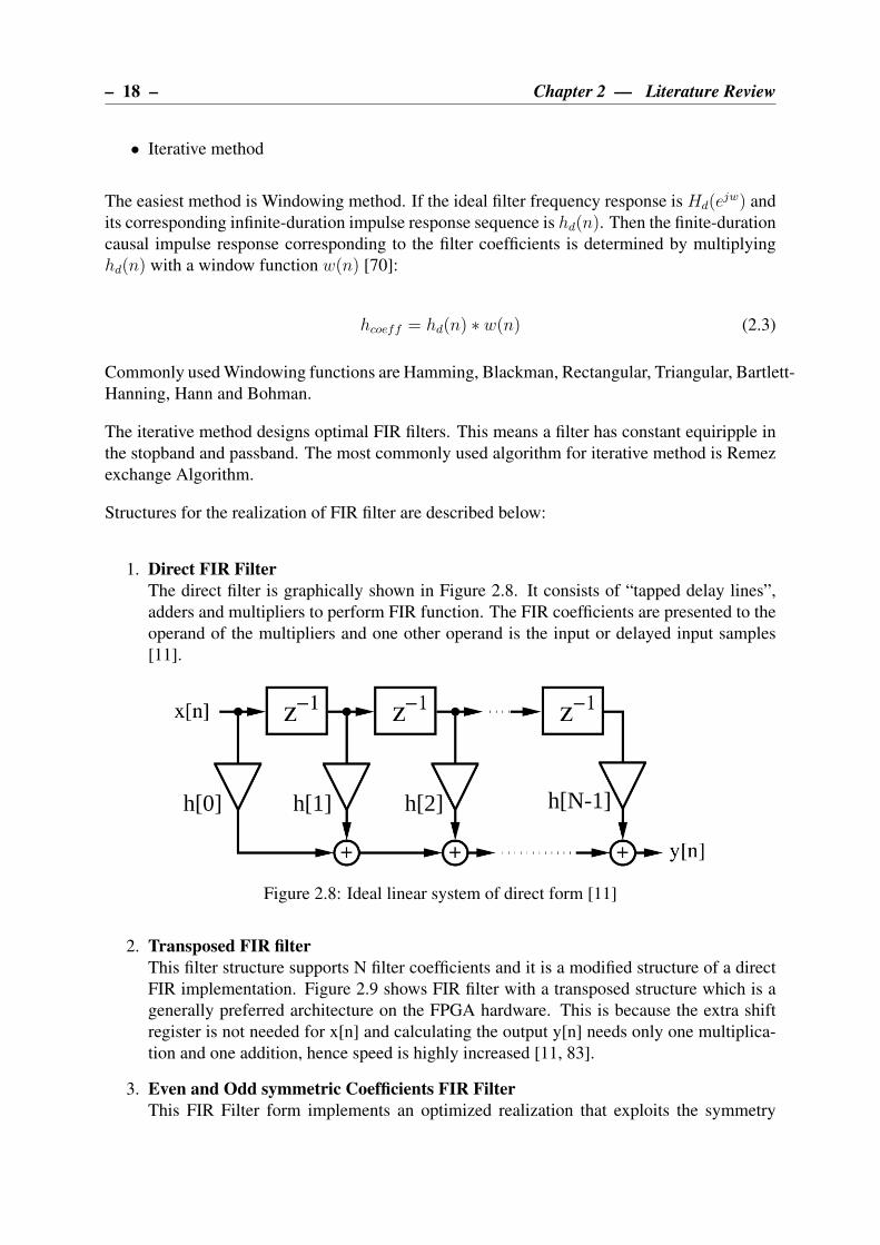
– 18 – Chapter 2 — Literature Review
• Iterative method
The easiest method is Windowing method. If the ideal filter frequency response is Hd(ejw) and
its corresponding infinite-duration impulse response sequence is hd(n). Then the finite-duration
causal impulse response corresponding to the filter coefficients is determined by multiplying
hd(n) with a window function w(n) [70]:
hcoeff = hd(n) ∗ w(n) (2.3)
Commonly used Windowing functions are Hamming, Blackman, Rectangular, Triangular, Bartlett-
Hanning, Hann and Bohman.
The iterative method designs optimal FIR filters. This means a filter has constant equiripple in
the stopband and passband. The most commonly used algorithm for iterative method is Remez
exchange Algorithm.
Structures for the realization of FIR filter are described below:
1. Direct FIR Filter
The direct filter is graphically shown in Figure 2.8. It consists of “tapped delay lines”,
adders and multipliers to perform FIR function. The FIR coefficients are presented to the
operand of the multipliers and one other operand is the input or delayed input samples
[11].
h[0] h[1] h[2] h[N-1]
Figure 2.8: Ideal linear system of direct form [11]
2. Transposed FIR filter
This filter structure supports N filter coefficients and it is a modified structure of a direct
FIR implementation. Figure 2.9 shows FIR filter with a transposed structure which is a
generally preferred architecture on the FPGA hardware. This is because the extra shift
register is not needed for x[n] and calculating the output y[n] needs only one multiplica-
tion and one addition, hence speed is highly increased [11, 83].
3. Even and Odd symmetric Coefficients FIR Filter
This FIR Filter form implements an optimized realization that exploits the symmetry

Chapter 2 — Literature Review – 19 –
h[N-1] h[N-2] h[N-3] h[0]
Figure 2.9: Transpose form FIR filter [11]
of frequency response coefficients. It reduces the number of multipliers to N/2 while
the number of adders remains unchanged. Consequently the filter with decreased area
footprint on the FPGA implementation is achieved [11, 59, 83]. Figure 2.10 shows the
parallel architectures of the symmetric coefficient FIR filters.
Figure 2.10: Optimised structures for linear-phase FIR filters (T = z−1: Sample period delay)
(i) FIR Symmetric structure when the filter order M is an odd number. (ii) FIR Symmetric
structure when the filter order M is an even number. [85]
4. Moving Average Filter
This FIR filter is illustrated in Figure 2.11 because of its wide usage in many communi-
cation systems[75]. Its output y[n] is defined by:
y[n] =1
N
N−1∑
k=0
x[n− k], (2.4)
where x[n] is the input data, k = 0, 1, ..., N − 1, and N is the filter length.
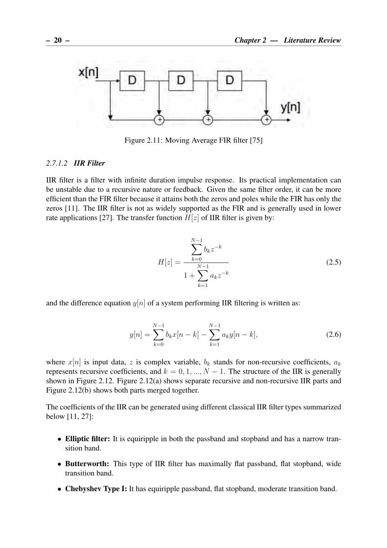
– 20 – Chapter 2 — Literature Review
Figure 2.11: Moving Average FIR filter [75]
2.7.1.2 IIR Filter
IIR filter is a filter with infinite duration impulse response. Its practical implementation can
be unstable due to a recursive nature or feedback. Given the same filter order, it can be more
efficient than the FIR filter because it attains both the zeros and poles while the FIR has only the
zeros [11]. The IIR filter is not as widely supported as the FIR and is generally used in lower
rate applications [27]. The transfer function H[z] of IIR filter is given by:
H[z] =
N−1∑
k=0
bkz−k
1 +N−1∑
k=1
akz−k
(2.5)
and the difference equation y[n] of a system performing IIR filtering is written as:
y[n] =N−1∑
k=0
bkx[n− k]−N−1∑
k=1
aky[n− k], (2.6)
where x[n] is input data, z is complex variable, bk stands for non-recursive coefficients, akrepresents recursive coefficients, and k = 0, 1, ..., N − 1. The structure of the IIR is generally
shown in Figure 2.12. Figure 2.12(a) shows separate recursive and non-recursive IIR parts and
Figure 2.12(b) shows both parts merged together.
The coefficients of the IIR can be generated using different classical IIR filter types summarized
below [11, 27]:
• Elliptic filter: It is equiripple in both the passband and stopband and has a narrow tran-
sition band.
• Butterworth: This type of IIR filter has maximally flat passband, flat stopband, wide
transition band.
• Chebyshev Type I: It has equiripple passband, flat stopband, moderate transition band.

Chapter 2 — Literature Review – 21 –
Figure 2.12: Generic structure of IIR filter [11]
• Chebyshev Type II: It has a flat passband, equiripple stopband, moderate transition band.
• Bessel: It is characterized by its fairly flat passband gain and slow initial rate of attenu-
ation. Bessel filters generally require higher filter order than other filters for satisfactory
stopband attenuation.
In fixed point arithmetic IIR realizations coefficients (a0...aN−1, b0...bN−1) are quantized, the
resulting errors can significantly alter the desired filter characteristics. Breaking up the IIR
transfer function into lower-order sections and connecting this in cascade or parallel can greatly
decrease the sensitivity to quantization errors [2].
One of the mostly used lower order IIR filters is a biquad. A biquad is a second order IIR filter
with two poles and two zeros [74]. The biquad can be used in a cascade to build higher order or
complex filters called second order sections (SOS). It is very useful for fixed point implemen-
tations as the effects of quantization and numerical stability are negligible [64]. The biquads
have two different forms namely Direct Form I and Direct Form II as shown in Figure 2.13. The
biquad IIR filter transfer function H[z] is defined by equation below:
H[z] =b0 + b1z
−1 + b2z−2
1 + a1z−1 + a2z−2(2.7)
where z is a complex variable, ak and bk are both filter coefficients. The difference equation
y[n] of a biquad is written as:
y[n] = b0x[n] + b1x[n− 1] + b2x[n− 2]− a1y[n− 1]− a2y[n− 2], (2.8)
where x[n] is input data.
Direct form I is the most preferred for fixed point arithmetic implementation because it has a
single summation point. Direct form II is suitable for floating point because it saves memory and

– 22 – Chapter 2 — Literature Review
Figure 2.13: Digital biquad filters [3]
it’s not sensitive to overflows in fixed point implementations. Direct form II can be enhanced
further with a transposed form which has better floating point accuracy [74].
2.7.2 FFT
Fast Fourier Transform (FFT) is an efficient implementation of Discrete Fourier Transform
(DFT). The function of a DFT is to map time domain data sequence into frequency domain data
sequence [73]. FFT is widely used and applies in many areas such as digital communication
systems, radar systems, multimedia systems etc. [73, 34, 81]. FFT output X[k] is defined by
the following equation:
X[k] =N−1∑
k=0
x[n]W nkN (2.9)
where k = 0, 1, ..., N − 1 and WN = e−j 2πN , the root-of-unity, is also known as the twiddle
factor.
FFTs can be realized in several architectures using various FFT algorithms. Factors such as
execution speed, hardware complexity, area occupation, flexibility and precision are considered
during FFT hardware implementation. Implementing parallel FFT architectures is very costly
although it leads to very high performance FFT. On the other hand serial implementations are
very slow which may not be ideal option for very high-speed real time systems. Pipelined
architectures have emerged as a better option as they present a trade-off between pure parallel
and pure serial implementations of FFT [73, 34, 81].
Radix-2, Radix-4, Radix-22 are amongst the commonly used FFT algorithms. These algo-
rithms are mapped into various forms of length-N FFT architectures which can be classified
into Single-path Delay Feedback (SDF), Single-path Delay Commutator (SDC), Multi-path
Delay Feedback (MDF) and Multi-path Delay Commutator (MDC). Some examples of archi-
tecture types are Radix-2 Multi-path Delay Commutator (R2MDC), Radix-2 Single-path Delay
Feedback (R2SDF), Radix-4 Single-path Delay Feedback (R4SDF), Radix-4 Multi-path De-
lay Commutator (R4MDC), Radix-4 Single-path Delay Commutator (R4SDC) and Radix-22
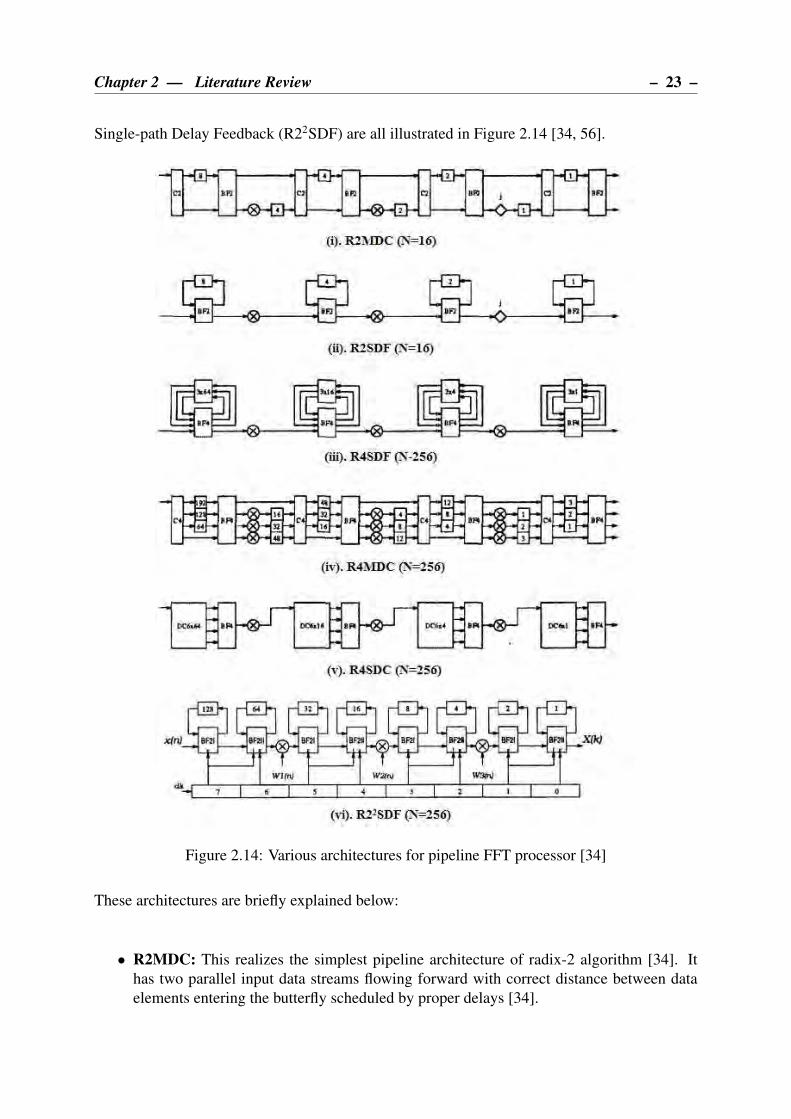
Chapter 2 — Literature Review – 23 –
Single-path Delay Feedback (R22SDF) are all illustrated in Figure 2.14 [34, 56].
Figure 2.14: Various architectures for pipeline FFT processor [34]
These architectures are briefly explained below:
• R2MDC: This realizes the simplest pipeline architecture of radix-2 algorithm [34]. It
has two parallel input data streams flowing forward with correct distance between data
elements entering the butterfly scheduled by proper delays [34].
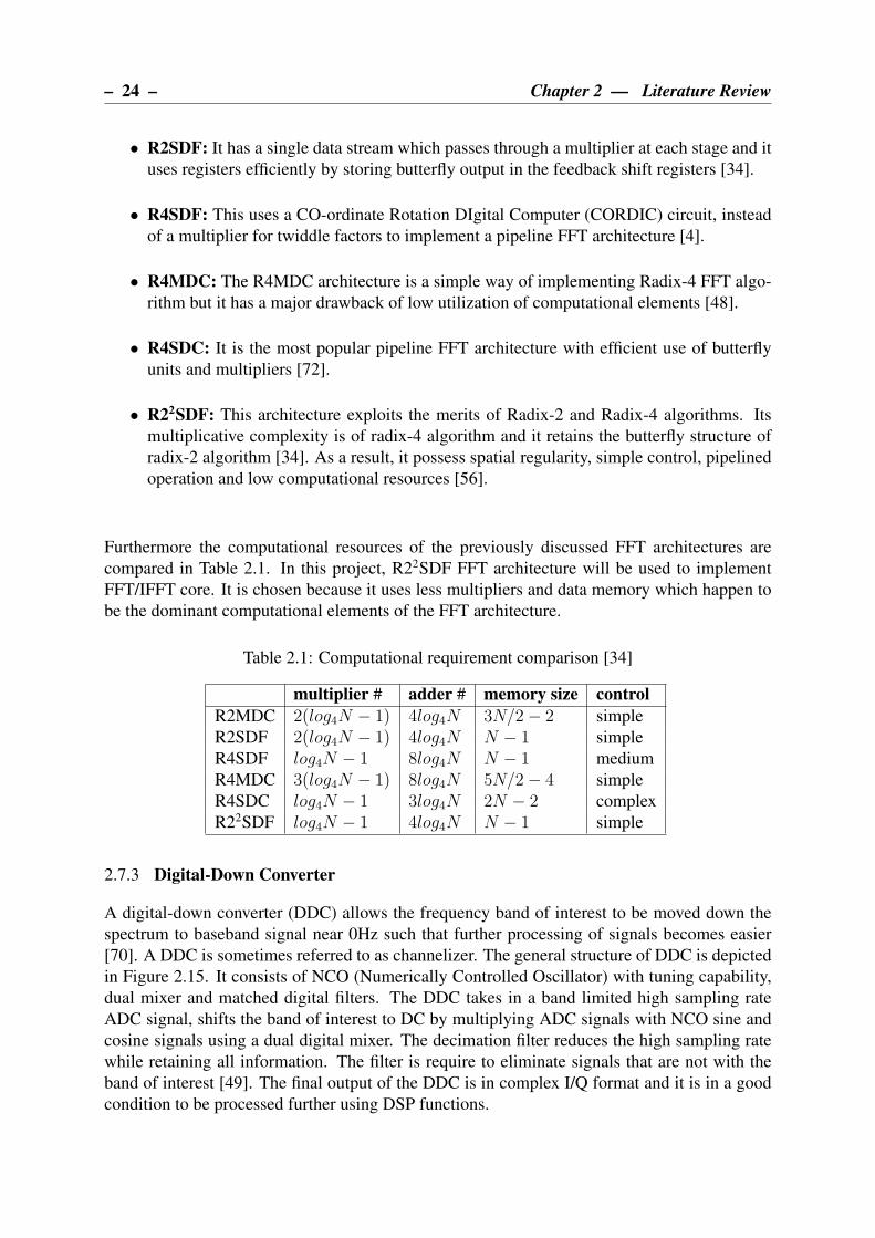
– 24 – Chapter 2 — Literature Review
• R2SDF: It has a single data stream which passes through a multiplier at each stage and it
uses registers efficiently by storing butterfly output in the feedback shift registers [34].
• R4SDF: This uses a CO-ordinate Rotation DIgital Computer (CORDIC) circuit, instead
of a multiplier for twiddle factors to implement a pipeline FFT architecture [4].
• R4MDC: The R4MDC architecture is a simple way of implementing Radix-4 FFT algo-
rithm but it has a major drawback of low utilization of computational elements [48].
• R4SDC: It is the most popular pipeline FFT architecture with efficient use of butterfly
units and multipliers [72].
• R22SDF: This architecture exploits the merits of Radix-2 and Radix-4 algorithms. Its
multiplicative complexity is of radix-4 algorithm and it retains the butterfly structure of
radix-2 algorithm [34]. As a result, it possess spatial regularity, simple control, pipelined
operation and low computational resources [56].
Furthermore the computational resources of the previously discussed FFT architectures are
compared in Table 2.1. In this project, R22SDF FFT architecture will be used to implement
FFT/IFFT core. It is chosen because it uses less multipliers and data memory which happen to
be the dominant computational elements of the FFT architecture.
Table 2.1: Computational requirement comparison [34]
multiplier # adder # memory size control
R2MDC 2(log4N − 1) 4log4N 3N/2− 2 simple
R2SDF 2(log4N − 1) 4log4N N − 1 simple
R4SDF log4N − 1 8log4N N − 1 medium
R4MDC 3(log4N − 1) 8log4N 5N/2− 4 simple
R4SDC log4N − 1 3log4N 2N − 2 complex
R22SDF log4N − 1 4log4N N − 1 simple
2.7.3 Digital-Down Converter
A digital-down converter (DDC) allows the frequency band of interest to be moved down the
spectrum to baseband signal near 0Hz such that further processing of signals becomes easier
[70]. A DDC is sometimes referred to as channelizer. The general structure of DDC is depicted
in Figure 2.15. It consists of NCO (Numerically Controlled Oscillator) with tuning capability,
dual mixer and matched digital filters. The DDC takes in a band limited high sampling rate
ADC signal, shifts the band of interest to DC by multiplying ADC signals with NCO sine and
cosine signals using a dual digital mixer. The decimation filter reduces the high sampling rate
while retaining all information. The filter is require to eliminate signals that are not with the
band of interest [49]. The final output of the DDC is in complex I/Q format and it is in a good
condition to be processed further using DSP functions.
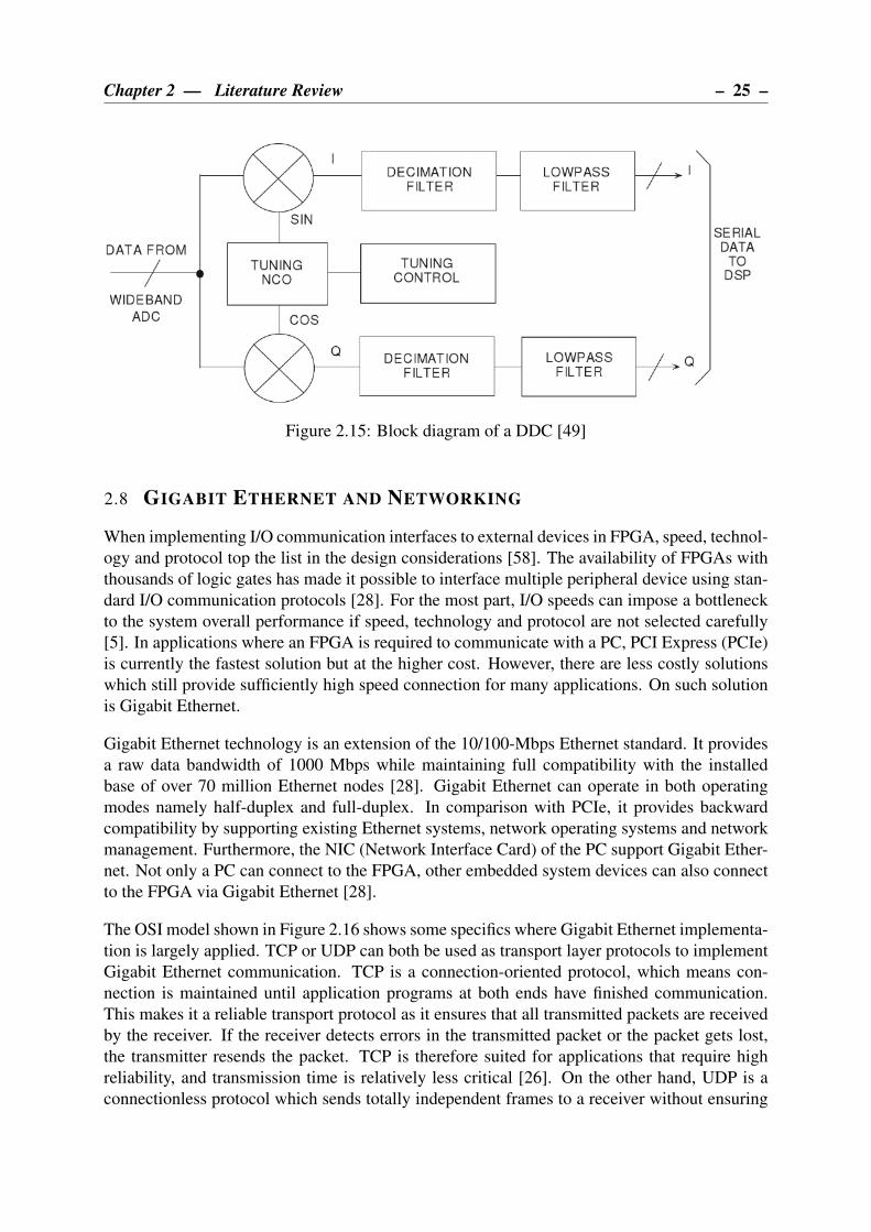
Chapter 2 — Literature Review – 25 –
Figure 2.15: Block diagram of a DDC [49]
2.8 GIGABIT ETHERNET AND NETWORKING
When implementing I/O communication interfaces to external devices in FPGA, speed, technol-
ogy and protocol top the list in the design considerations [58]. The availability of FPGAs with
thousands of logic gates has made it possible to interface multiple peripheral device using stan-
dard I/O communication protocols [28]. For the most part, I/O speeds can impose a bottleneck
to the system overall performance if speed, technology and protocol are not selected carefully
[5]. In applications where an FPGA is required to communicate with a PC, PCI Express (PCIe)
is currently the fastest solution but at the higher cost. However, there are less costly solutions
which still provide sufficiently high speed connection for many applications. On such solution
is Gigabit Ethernet.
Gigabit Ethernet technology is an extension of the 10/100-Mbps Ethernet standard. It provides
a raw data bandwidth of 1000 Mbps while maintaining full compatibility with the installed
base of over 70 million Ethernet nodes [28]. Gigabit Ethernet can operate in both operating
modes namely half-duplex and full-duplex. In comparison with PCIe, it provides backward
compatibility by supporting existing Ethernet systems, network operating systems and network
management. Furthermore, the NIC (Network Interface Card) of the PC support Gigabit Ether-
net. Not only a PC can connect to the FPGA, other embedded system devices can also connect
to the FPGA via Gigabit Ethernet [28].
The OSI model shown in Figure 2.16 shows some specifics where Gigabit Ethernet implementa-
tion is largely applied. TCP or UDP can both be used as transport layer protocols to implement
Gigabit Ethernet communication. TCP is a connection-oriented protocol, which means con-
nection is maintained until application programs at both ends have finished communication.
This makes it a reliable transport protocol as it ensures that all transmitted packets are received
by the receiver. If the receiver detects errors in the transmitted packet or the packet gets lost,
the transmitter resends the packet. TCP is therefore suited for applications that require high
reliability, and transmission time is relatively less critical [26]. On the other hand, UDP is a
connectionless protocol which sends totally independent frames to a receiver without ensuring

– 26 – Chapter 2 — Literature Review
Figure 2.16: The OSI and generic Ethernet Physical Model [50]
their arrival at the destination. As a result it is unreliable transport protocol as lost packets
are never retransmitted by a sender. Since UDP sends packets without error and flow control,
overhead and latency are low. It is therefore suitable for applications that need fast and efficient
transmission such as real-time applications [26].
Typically, IPv4 is used as network layer along with one of the transport layer protocols. Since
many streaming applications involving FPGA and PC do not require retransmission of packets
in the communication, UDP is preferred [58, 6] to TCP for the following reasons:
• It uses a simpler protocol mechanism without special handshaking between sender and
receiver.
• It is suitable for streaming applications because of its minimal delay in transmission of
packets.
• It uses less resources on FPGA and it is simple to implement
Although the UDP is a preferred transport protocol in many FPGA streaming applications, the
user needs to ensure that the sender does not overwhelm the receiver with frames as this is
likely to result in dropped frames [26] at receiver end. The corrupted frames will fail CRC at
the receiver and will also be discarded.
Moreover, a physical layer device (PHY) is required for FPGA to connect with external devices.
This is located on the board between the FPGA and the interface to external devices. Nowadays
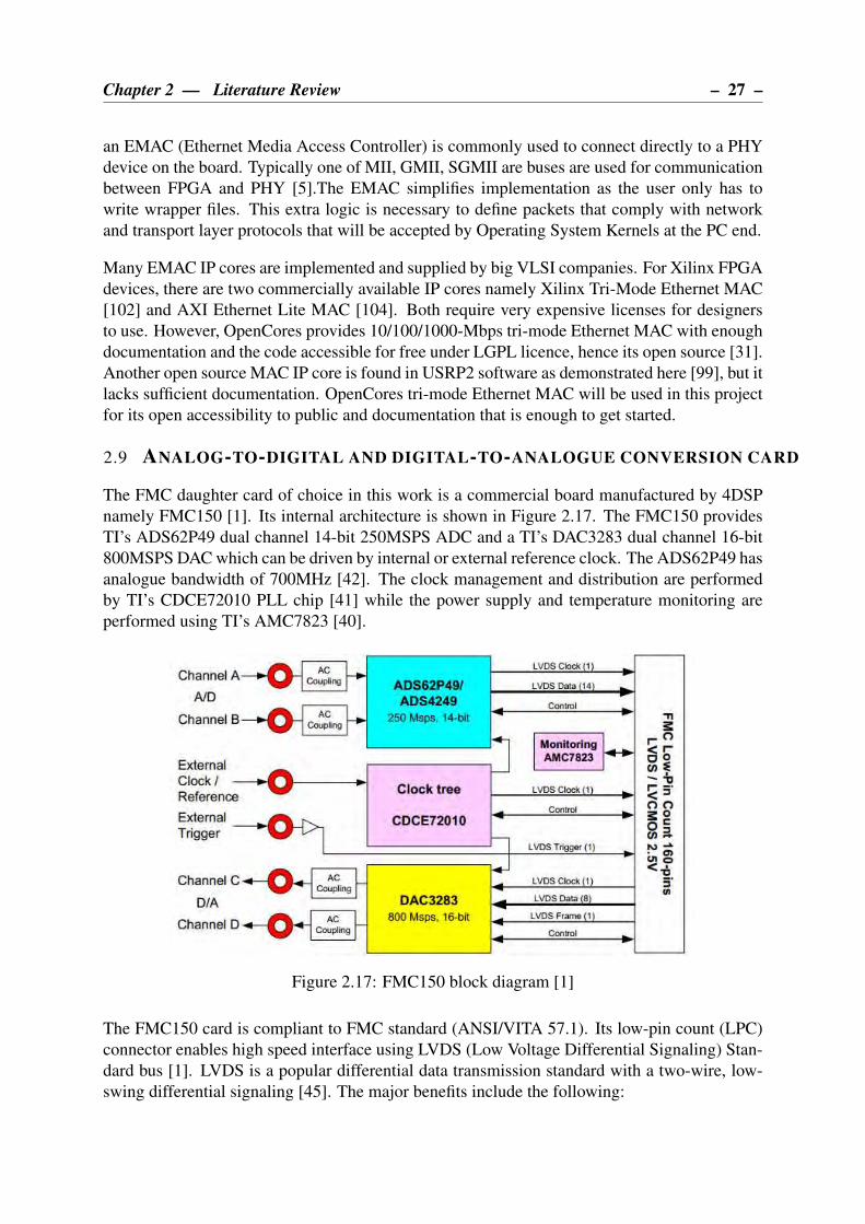
Chapter 2 — Literature Review – 27 –
an EMAC (Ethernet Media Access Controller) is commonly used to connect directly to a PHY
device on the board. Typically one of MII, GMII, SGMII are buses are used for communication
between FPGA and PHY [5].The EMAC simplifies implementation as the user only has to
write wrapper files. This extra logic is necessary to define packets that comply with network
and transport layer protocols that will be accepted by Operating System Kernels at the PC end.
Many EMAC IP cores are implemented and supplied by big VLSI companies. For Xilinx FPGA
devices, there are two commercially available IP cores namely Xilinx Tri-Mode Ethernet MAC
[102] and AXI Ethernet Lite MAC [104]. Both require very expensive licenses for designers
to use. However, OpenCores provides 10/100/1000-Mbps tri-mode Ethernet MAC with enough
documentation and the code accessible for free under LGPL licence, hence its open source [31].
Another open source MAC IP core is found in USRP2 software as demonstrated here [99], but it
lacks sufficient documentation. OpenCores tri-mode Ethernet MAC will be used in this project
for its open accessibility to public and documentation that is enough to get started.
2.9 ANALOG-TO-DIGITAL AND DIGITAL-TO-ANALOGUE CONVERSION CARD
The FMC daughter card of choice in this work is a commercial board manufactured by 4DSP
namely FMC150 [1]. Its internal architecture is shown in Figure 2.17. The FMC150 provides
TI’s ADS62P49 dual channel 14-bit 250MSPS ADC and a TI’s DAC3283 dual channel 16-bit
800MSPS DAC which can be driven by internal or external reference clock. The ADS62P49 has
analogue bandwidth of 700MHz [42]. The clock management and distribution are performed
by TI’s CDCE72010 PLL chip [41] while the power supply and temperature monitoring are
performed using TI’s AMC7823 [40].
Figure 2.17: FMC150 block diagram [1]
The FMC150 card is compliant to FMC standard (ANSI/VITA 57.1). Its low-pin count (LPC)
connector enables high speed interface using LVDS (Low Voltage Differential Signaling) Stan-
dard bus [1]. LVDS is a popular differential data transmission standard with a two-wire, low-
swing differential signaling [45]. The major benefits include the following:

– 28 – Chapter 2 — Literature Review
• Posibbility of low supply voltage operation
• High speed data transfer
• Good common noise rejection
• Less noise generation
2.10 ADC NOISE SPECIFICATIONS
The ADC introduces noise and distortion that degrades the quality of a sampled analogue sig-
nal. The ADC parameters provide designers a fairly accurate correlation of the performance
expectations of a particular ADC [36]. These parameters are classified into two namely static
parameters and dynamic parameters. The common static parameters include offset error, gain
error, differential nonlinearity (DNL) and integral nonlinearity. Dynamic parameters include
signal to noise ratio (SNR), signal to noise and distortion ratio (SINAD), effective number of
bits (ENOB), total harmonic distortion (THD) and spurious-free dynamic range (SFDR) [13].
The static parameters are of most significance in extremely low frequency signals compared
to sampling frequency. Static parameter effects are less important in high frequency applica-
tions, for this reason the dynamic parameters apply. SDR applications typically operate at very
high frequencies therefore only dynamic parameters are detailed in this literature. Both the
theoretical and mathematical descriptions of dynamic parameters are presented as follows [36]:
• Signal-to-Noise Ratio (SNR): This characterizes the ratio of the fundamental signal to
the noise spectrum. It is the sum of all spectral components except DC, fundamental and
the first six harmonics relative to full-scale power (dBFS) or signal power (dBc). It is
defined by equation 2.10.
SNR = 6.02 ·N + 1.763 (dB) (2.10)
where N is the ADC resolution.
• Signal-to-Noise And Distortion (SINAD): It is the combination of SNR and THD, that
is, the sum of all spectral components except DC and fundamental relative to the signal
power measure in dBc. It is defined by equation 2.11.
SINAD = 20 · log10(
Asignal[rms]
Anoise[rms]
)
(dB) (2.11)
where Asignal is the RMS value of the signal input to ADC and Anoise is the RMS value of
the noise including the harmonic content.
• Effective Number of Bits (ENOB): This is a figure of merit which tells how close the
ADC is near to the theoretical mathematical model. It calculated from SINAD using
equation 2.12.
Chapter 2 — Literature Review – 29 –
ENOB =SINAD − 1.763
6.02(bits) (2.12)
where all values are given in dB, and SINAD is the signal-to-noise and distortion ratio,
6.02 is to convert decibels (log10) to bits (log2), and 1.763 is the quantization error in an
ideal ADC.
• Total Harmonic Distortion (THD): This characterizes the ratio of the sum of power
of the first six harmonics to the fundamental signal power. It is measured in (dBc) and
defined by equation 2.13.
THD = 20 · log10(
√
V 22 + V 2
3 + · · ·+ V 2X
V1
)
(dBc) (2.13)
where V2 to VX are harmonics to the fundamental V1.
• Spurious Free Dynamic Range (SFDR): This is the ratio of the level of the input signal
to the level of the largest distortion components in the FFT spectrum. It is measured in
dBc and is defined by equation 2.14.
SFDR = 20 · log10(
Vf
Vs
)
(dBc) (2.14)
where Vf is a fundamental signal and Vs is highest spurious signal.
2.11 FREQUENCY MODULATION AND DEMODULATION
Frequency modulation is a type of angle modulation where frequency of the carrier is varied ac-
cording to the amplitude of the information (message) signal [12]. The instantaneous frequency
fi of carrier is varied linearly with the message m(t)
fi =1
2π
dθi(t)
dt=
1
2πθi(t) = fc + kvco ·m(t) (2.15)
where amplitude and phase of carrier are constant. kvco is the voltage-to-frequency gain of the
VCO (Voltage Controlled Oscillator) expressed in units of Hz/V, and the quantity, kvco ×m(t),is the instantaneous frequency deviation. The frequency-modulated waveform is expressed as
shown below
xFM = Accos
[
2πfct+ 2πkvco
∫ t
0
m(τ)dτ
]
(2.16)
where
• xFM is FM output signal.
• fc is the carrier frequency (i.e. frequency of unmodulated signal).
• Ac is carrier signal amplitude.
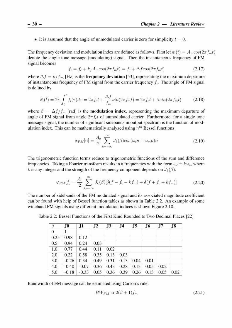
– 30 – Chapter 2 — Literature Review
• It is assumed that the angle of unmodulated carrier is zero for simplicity t = 0.
The frequency deviation and modulation index are defined as follows. First let m(t) = Amcos(2πfmt)denote the single-tone message (modulating) signal. Then the instantaneous frequency of FM
signal becomes
fi = fc + kfAmcos(2πfmt) = fc +∆fcos(2πfmt) (2.17)
where ∆f = kfAm [Hz] is the frequency deviation [53], representing the maximum departure
of instantaneous frequency of FM signal from the carrier frequency fc. The angle of FM signal
is defined by
θi(t) = 2π
∫ t
0
fi(τ)dτ = 2πfct+∆f
fmsin(2πfmt) = 2πfct+ βsin(2πfmt) (2.18)
where β = ∆f/fm [rad] is the modulation index, representing the maximum departure of
angle of FM signal from angle 2πfct of unmodulated carrier. Furthermore, for a single tone
message signal, the number of significant sidebands in output spectrum is the function of mod-
ulation index. This can be mathematically analyzed using nth Bessel functions
xFM [n] =Ac
2
∞∑
k=−∞
Jk(β)cos(ωcn+ ωmk)n (2.19)
The trigonometric function terms reduce to trigonometric functions of the sum and difference
frequencies. Taking a Fourier transform results in a frequencies with the form ωc ± kωm where
k is any integer and the strength of the frequency component depends on Jk(β).
ϕFM [f ] =Ac
2
∞∑
k=−∞
Jk(β)[δ(f − fc − kfm) + δ(f + fc + kfm)] (2.20)
The number of sidebands of the FM modulated signal and its associated magnitude coefficient
can be found with help of Bessel function tables as shown in Table 2.2. An example of some
wideband FM signals using different modulation indices is shown Figure 2.18.
Table 2.2: Bessel Functions of the First Kind Rounded to Two Decimal Places [22]
β J0 J1 J2 J3 J4 J5 J6 J7 J8
0 1
0.25 0.98 0.12
0.5 0.94 0.24 0.03
1.0 0.77 0.44 0.11 0.02
2.0 0.22 0.58 0.35 0.13 0.03
3.0 -0.26 0.34 0.49 0.31 0.13 0.04 0.01
4.0 -0.40 -0.07 0.36 0.43 0.28 0.13 0.05 0.02
5.0 -0.18 -0.33 0.05 0.36 0.39 0.26 0.13 0.05 0.02
Bandwidth of FM message can be estimated using Carson’s rule:
BWFM ≈ 2(β + 1)fm (2.21)
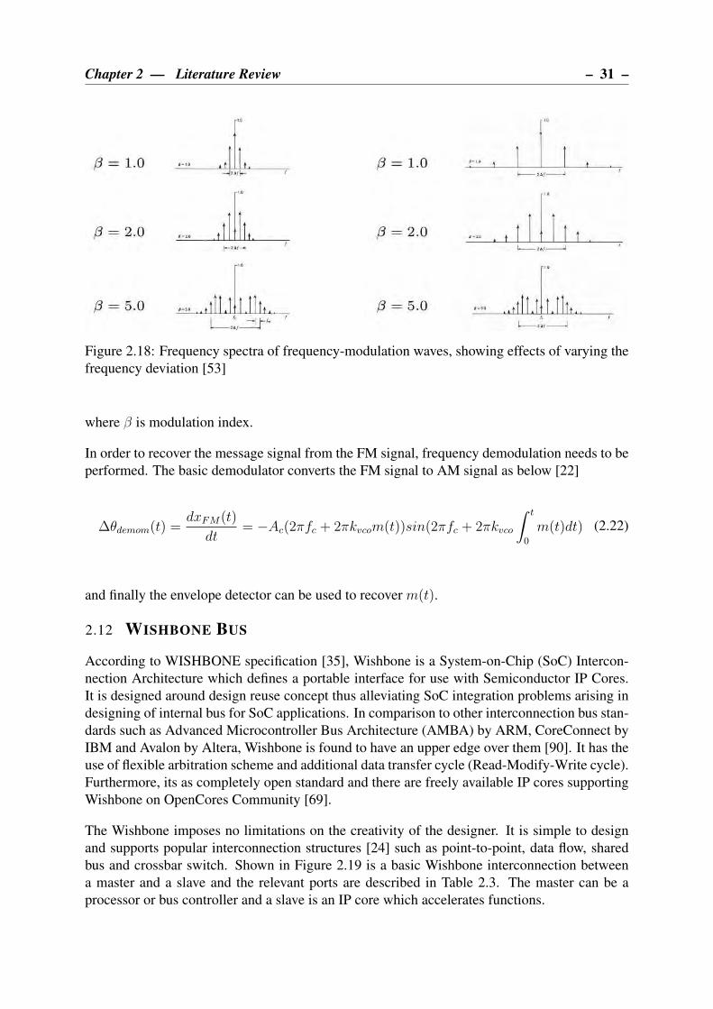
Chapter 2 — Literature Review – 31 –
Figure 2.18: Frequency spectra of frequency-modulation waves, showing effects of varying the
frequency deviation [53]
where β is modulation index.
In order to recover the message signal from the FM signal, frequency demodulation needs to be
performed. The basic demodulator converts the FM signal to AM signal as below [22]
∆θdemom(t) =dxFM(t)
dt= −Ac(2πfc + 2πkvcom(t))sin(2πfc + 2πkvco
∫ t
0
m(t)dt) (2.22)
and finally the envelope detector can be used to recover m(t).
2.12 WISHBONE BUS
According to WISHBONE specification [35], Wishbone is a System-on-Chip (SoC) Intercon-
nection Architecture which defines a portable interface for use with Semiconductor IP Cores.
It is designed around design reuse concept thus alleviating SoC integration problems arising in
designing of internal bus for SoC applications. In comparison to other interconnection bus stan-
dards such as Advanced Microcontroller Bus Architecture (AMBA) by ARM, CoreConnect by
IBM and Avalon by Altera, Wishbone is found to have an upper edge over them [90]. It has the
use of flexible arbitration scheme and additional data transfer cycle (Read-Modify-Write cycle).
Furthermore, its as completely open standard and there are freely available IP cores supporting
Wishbone on OpenCores Community [69].
The Wishbone imposes no limitations on the creativity of the designer. It is simple to design
and supports popular interconnection structures [24] such as point-to-point, data flow, shared
bus and crossbar switch. Shown in Figure 2.19 is a basic Wishbone interconnection between
a master and a slave and the relevant ports are described in Table 2.3. The master can be a
processor or bus controller and a slave is an IP core which accelerates functions.

– 32 – Chapter 2 — Literature Review
Figure 2.19: Wishbone bus basic connection [35]
2.13 CONCLUSIONS
This chapter reviewed SDR to provide a theoretical understanding needed before developing
applications using RHINO platform. The reconfigurable computing was then highlighted in
the context of SDR to show how it can be applied to achieve high performance computing
capabilities. Thereafter, different reconfigurable computing devices such as GPP, ASIC and
FPGA were studied and analysed in terms providing better performance when used in SDR
applications. GPP is still popular because of its low cost, high flexibility and simplicity but
at the cost of low performance. ASICs have very high performance capabilities but are very
expensive. FPGA is therefore a reconfigurable device of choice in SDR because it is less costly
and offers advanced computing capabilities with flexibility.
Due to increasing popularity of FPGAs, IP designers increasingly demand ready-made library
of IP cores to integrate in SDR applications. Consequently, a concept of IP Reuse becomes very
important and this was discussed in this chapter along with the latest trend of IP libraries. When
investigating these IP libraries, it has been discovered that many of the robust and reliable IP
cores are sold by commercial IP companies at high costs. There are also freely available IP cores
offered by open-source communities, but these IP libraries lack support and documentation
making it hard to use. The library of IP cores to be developed in this project will therefore
build on strengths and weaknesses found in existing libraries studied in this chapter. The IP
cores will be highly reusable, well documented, and completely free and will be available under
open-source license.

Chapter 2 — Literature Review – 33 –
Table 2.3: Signal description of Wishbone bus
Signal Name Description
RST I reset input Global active high reset signal.
CLK I clock input Global clock signal.
ADR O/I address output/input array The address bus from master to slave.
DAT I/O Data input/output array Data bus from slave to master.
DAT O/I Data output/input array Data bus from master to slave.
WE O/I Write enable output/input The write enable signal from master to slave. It
is asserted by master during write operation and
negated during read operation.
STB O/I strobe output/input Indicates a valid data transfer cycle and it is as-
serted by the master.
ACK I/O acknowledge input/output Indicates a normal termination of a bus cycle
when set by a slave.
CYC O/I cycle output/input Indicates a valid bus cycle is in progress when
set by a master.
Furthermore, VHDL was introduced in this chapter because it is a hardware description lan-
guage of choice that will be used to develop FPGA-synthesizable cores in this project. It is
also a conventional language used in previous projects developed for RHINO. RHINO platform
targets SDR domain applications namely Radio Astronomy, Radar and Telecommunications.
These were briefly reviewed in this chapter to help identify IP cores for this project that will
meet target application requirements.
As specified in Chapter 1, the IP cores in this project will be classified into DSP cores and I/O
interface cores. The DSP cores will be based on DSP algorithms namely IIR, FIR, FFT/IFFT
and DDC. The review of these algorithms was covered in this chapter and different techniques
to implement them efficiently on the FPGA were covered. As a result, the proposed IP core
library will use the same development techniques to achieve efficiency, high performance and
reusability of the IP cores. Furthermore, a Wishbone bus was also discussed because it will be
used as standard a interconnection bus for the DSP cores in this project. It is chosen because it
has plenty of support by the Open-Cores community and it is completely open-source.
Additionally, the high speed FMC150 ADC/DAC daughter-card was reviewed. The interface
controller for this will be developed to enable RHINO to perform ADC and DAC operations.
Also the introduction to ADC dynamic parameters was discussed as they will be used later in
this project to evaluate the performance characteristics of the FMC150 card. In order to ship
high volumes of digital data from RHINO to external devices or a PC, the 1 Gigabit Ethernet in-
terface core will be developed. Speed, technology and protocol used when developing Ethernet
interface core for FPGAs were discussed in this chapter. Although 1 Gigabit Ethernet supports
three speeds 10, 100 and 1000 Mbps, in this project only 1000 Mbps will be considered when
developing the Ethernet interface core. UDP was found to be a commonly used Transport layer
protocol in many FPGA platforms involving Ethernet interface. We will also use UDP to de-
velop 1 Gigabit Ethernet interface for RHINO. We choose UDP because it incurs low latency
and overhead which will be ideal for high speed streaming and real-time SDR applications. It

– 34 – Chapter 2 — Literature Review
is also simple to implement hence this will save us plenty of time. However, it has a major
drawback of unreliability due to lack of data flow control, this will be avoided by carefully
choosing transmission rates tolerable by the receiver. The core will be developed with the aid
of Open-Cores Tri-mode MAC core which was also discussed in this chapter. This MAC core
is open-source and has continuous support.

CHAPTER 3
METHODOLOGY
This chapter starts off with details of the requirements analysis for the library of SDR IP blocks.
It then goes on to discuss the design process and operational design for the proposed library.
Thereafter, it describes both hardware and software tools that will be used in order to pave the
way for the best development and testing environment. Then the final section overviews the
experimental test for each of the designed IP blocks.
3.1 USER REQUIREMENTS FOR IP BLOCKS LIBRARY
The main purpose if this section is to provide a better understanding of the user requirements
regarding the proposed library of IP cores. These requirements were studied from intensive lit-
erature conducted [10][25][29][71][100], in particular the requirements which are common in
SDR applications such as Telecommunications, Radar and Radio Astronomy. The user require-
ments are divided into functional requirements and non-functional requirements of the SDR
blocks.
3.1.1 Functional Requirements
The functional requirements describe behaviour expected of IP blocks or cores to be designed
and implemented. The functional requirements are outlined as follows:
• The SDR blocks will perform DSP operations common in SDR applications and provide
interface to connect the FPGA to external devices through high speed I/O communication
ports or adapters.
• The blocks will be capable of capturing digitized data from the ADC card and sending
out the digital data using DAC card.
• The blocks will be able to operate in a streaming mode where the ADC data will be cap-
tured and be shipped off the FPGA via 1 Gigabit Ethernet using UDP at high throughput
speed typically used in SDR applications.
• The cores will not depend on a specific high level CAD tool.
35
– 36 – Chapter 3 — Methodology
• Each core will provide a simple parallel interface to enable high speed interconnection
with other cores.
• The blocks will possess a hardwired control for failure protection.
• Apart from 100MHz clock provided by the system, the SDR blocks will reliably operate
in the clock frequency range of 312.5kHz to 375MHz.
The above functional requirements will ensure that the IP blocks are developed in accordance
with the project objectives as outlined in section 1.4.
3.1.2 Non-Functional Requirements
The non-functional requirements describe the metrics and constraints to measure the success of
the developed SDR blocks. These non-functional requirements are outlined as below:
• The library of IP blocks will be publicly accessible under open source license.
• The blocks will be reusable and parameterizable for integration in many SDR applica-
tions.
• The blocks will be easily upgradable, scalable and portable.
• For parallel and cascaded IP core architectures, replication of sub-blocks will be applied.
• The system clock or cycle time will be adjustable to a working environment.
• The Wishbone slave interface for each DSP core will be defined; however, no tests will
be made in a real SoC design environment.
These non-functional requirements are necessary for user to evaluate the degree to which the
objectives outlined in section 1.4 have been met.
3.2 DOMAIN REQUIREMENTS
In order to ensure that all the SDR blocks conform to the same standards and consistent general
functionality, the domain requirements describe the rules and actions needed when developing
the blocks. Domain requirements are outlined below:
• Each IP block and relating sub-blocks will be completed with a synthesizable source code
in VHDL.
• The IP block will be self-contained, that is, external dependencies such as elements, de-
sign units and packages will be avoided.

Chapter 3 — Methodology – 37 –
• General functionality of each core will be technology independent, using VHDL code.
However, the exception is in technology specific applications such as Xilinx spartan6
where adhoc HDL primitives and libraries are used for management and routing of clock
and external I/O pins.
• Each core will have a testbench showing the tests passed and will be accompanied by
MATLAB scripts that generate input vectors for the core in the testbench. The scripts
will also create an ideal model for a core under test, therefore the ideal model results will
be compared with testbench results.
• Clock and reset signal will contain no combinational logic.
• Each DSP core will have en and vld pins. The en port will be used to enable or disable a
global system clock while vld port will signal the availability of valid output sample from
the core.
• Bidirectional ports will not be used. Both input and output ports will be separate.
3.3 DESIGN PROCESS
The high level design process for RHINO IP blocks is detailed in section 1.5 and illustrated in
Figure 1.2. In this project, the behavioral model of the blocks will be designed in Xilinx ISE
and this fits in “develop behavioral model” block of the design process shown in Figure 1.2.
It is therefore important to understand the ISE design flow of the IP cores in the context of
development for RHINO and this is illustrated in Figure 3.1. This comprises a number of steps
which are: design entry, functional verification, design synthesis, design implementation, and
Xilinx device programming [101].
Design entry involves creating a new project using the ISE and adding timing constraints, pin
assignments, and area constraints of the IP block being designed.
Functional verification entails verification of the design at different points of the ISE design
flow. The first verification occurs before synthesis and is called behavioral simulation (also
known as RTL simulation) as shown Figure 3.1. A second verification uses SIMPRIM library,
it takes place after translation and it is called functional simulation (also known as gate-level
simulation). The last verification is in-circuit verification which happens after device program-
ming.
Design synthesis converts HDL design to a flat netlist which describes the connection of logic
gates which make the system.
Design Implementation undergoes translate, map, place and route processes.
Timing Verification is performed by running static timing and timing simulation.
Xilinx Device Programming involves creating a bitstream file and converting it to “.bof” file
executable in BORPH operating sytem (OS). The “.bof” file is run like a normal linux C appli-
cation as software process in BORPH operating system.

– 38 – Chapter 3 — Methodology
Design Entry
Design Synthesis
Design Implementation
Functional Simulation
Static Timing Simulation
Timing Simulation
Back Annotation
Xilinx Device Programming
In-Circuit Verification
Behavioral Simulation
Design Verification
Figure 3.1: FPGA Design Flow using Xilinx ISE [101]
3.4 OPERATIONAL DESIGN
The overall system architecture of RHINO SDR processing blocks is shown in Figure 3.2. All
the blocks will be designed in VHDL and run on the spartan6-XC6SLX150T FPGA device of
RHINO board. The reason for using VHDL to describe the logic of SDR blocks is because it is
a standard HDL language for RHINO gateware projects. Furthermore, previous FPGA projects
for RHINO have been developed in VHDL.
ADC interface
DAC interface
Digital Filtering - FIR core - IIR core
Fourier Transform : - FFT core - IFFT core
Data Rate conversion - DDC core
Case study : - Digital Wideband FM Receiver
1Gbps Ethernet interface
- Data acquisition using Tcpdump and Wireshark
- Data analysis by plotting FFT and PSD graphs in MATLAB
ADC
DAC
PC4DSP FMC150
RHINO: Spartan 6 FPGA
Sample rate = 163.84 MSPS
Sample rate = 61.44 MSPS
Figure 3.2: Architecture of RHINO SDR processing blocks
The design of IP cores will be categorized into two, namely DSP and I/O processing blocks
or cores. The flow chart showing design process for each IP core is illustrated in Figure 3.3.
The functionality and performance of the building library of SDR blocks will be exemplified

Chapter 3 — Methodology – 39 –
by designing a prototype of a digital wideband FM receiver which will be built from developed
SDR blocks. The IP blocks are shown in Figure 3.2 and are briefly described below:
What is IP core type?
start
Floating point Model in Matlab and
Test-bench
DSP Algorithm Evaluation
Algorithm Verified?
Convert floating point algorithm to fixed-point
FPGA structure
Fixed point algorithm Model in VHDLand
Test-bench
Fixed-point algorithm FPGA implementation
Algorithm Verified?
Study Device/interface Datasheet
I/O Interface core in VHDL and
Test-bench
Develop I/O interface core
Hardware Integration and On-board Testing
Does I/O interface
core work?
FPGA prototyping
Finish
I/O Interface core (FMC150 and Gigabit Ethernet)
DSP core (FIR, IIR, FFT, iFFT and DDC)
Yes
No
No
Yes
Yes
No
Figure 3.3: IP core design process
3.4.1 DSP blocks
By employing common DSP algorithms used in many areas of SDR, the DSP cores were chosen
and classified as below:
3.4.1.1 Digital Filtering
The digital filtering cores to be developed are used in many SDR applications if not all. With
support of multiple realizable structures of filters on the FPGA, the cores offer flexibility and
broad choice of filter solutions for different design environments. The filter cores to be designed
in this project are listed below:

– 40 – Chapter 3 — Methodology
• FIR core implements the FIR filter on the FPGA. It is chosen because it can achieve the
exact linear response with unconditional stability [16], hence it is the most popular digital
building block in SDR. It also forms the most computationally intensive part of the SDR
namely the channelizer or IF (Intermediate Frequency) processing block.
• IIR core implements the IIR filter on the FPGA. It is chosen because it can achieve the
same magnitude response of an FIR filter using lower order design [16]. Thus it can
be the best alternative in SDR applications where resources are insufficient and fewer
computations are needed.
3.4.1.2 Fourier Transform
The Fast Fourier Transform is another fundamental building block of SDR-based DSP systems.
Although the algorithm analysis may seem straight-forward, implementing this efficiently on
the FPGA can be challenging. The architecture which comprises parallel and pipeline char-
acteristics is realized using both Fast Fourier Transform and Inverse Fast Fourier Transform
algorithms. The core is described below:
• FFT/IFFT core is implemented using FFT and IFFT algorithm on the FPGA. This core
will be designed because it is popularly used in SDR applications such OFDM, Radar,
multimedia and efficient channelizer implementations.
3.4.1.3 Channelization
Channelization is made up of channellizer and it is typically the most computationally intensive
[98] part of the SDR receiver as it performs IF processing at highest sampling rate. A digital
down converter algorithm is often used to build a channelizer and in this project the core below
will be designed.
• DDC core will perform data rate conversion and frequency downshifting using a digital
down converter algorithm.
3.4.2 I/O blocks
The I/O cores are responsible for input and output data communication between the FPGA and
peripheral or external devices. The I/O cores to be developed are listed below:
• 1 Gigabit Ethernet core
• ADC-DAC interface core

Chapter 3 — Methodology – 41 –
3.4.3 Digital Wideband FM receiver
The application will be designed to demonstrate that not only developed SDR blocks will be
used in the FM receiver, but also in other real time SDR applications. It does so by using the
developed library of blocks that include the ADC core, DDC core and 1 Gigabit Ethernet core.
The I/Q FM demodulator will be implemented in Matlab on the PC and will acquire input from
FM samples streamed from the FPGA via 1 Gigabit Ethernet.
3.5 EXPERIMENTAL ENVIRONMENT
The experimental development process will follow the flowchart in Figure 3.4. First the fixed
point model test will be performed in Matlab as an ideal reference before performing each
DSP core test. The DDC core test depends on the FIR core test. After testing all DSP cores, the
process continues to 1 Gigabit Ethernet Interface core and later the FMC150 interface core. This
is followed by a streaming core which depends on the results obtained from 1 Gigabit Ethernet
and FMC150 interface cores. The DDC core, 1 Gigabit Ethernet and FMC150 interface cores
need to be tested before performing the last cumulative experiment of the FM receiver.
exp1
exp4
exp3
exp2
exp5
exp6 exp7
exp8
exp9
exp1 – Matlab Floating point Model Tests
exp2 – FIR core Test
exp3 – IIR core Testexp4 – FFT/IFFT core Testexp5 – DDC core Testexp6 – 1Gbps Ethernet Interface core Testexp7 – FMC150 (ADC/DAC) Interface core Test
exp8 – FMC150-Ethernet Streaming mode Test
exp9 – FM Receiver Test
Figure 3.4: A flowchart showing experimental development process
A considerable number of hardware and software tools will be used to aid with the development
and setting up of the experimental environment. The hardware tools include a Desktop PC,
RHINO board, oscilloscope, function generator, spectrum analyzer and xilinx platform cable.
The software tools are Xilinx ISE 14.7, ISim, ChipScope Pro, Tcmpdump, Wireshark, Matlab,
ADCPro and Speedometer. All these hardware and software tools are further elaborated below.
3.5.1 Hardware
This section lists the hardware tools and their specifications below:
• Desktop Computer: A high performance machine is required for FPGA-based develop-
– 42 – Chapter 3 — Methodology
ment work and to run memory demanding as well as processor intensive software appli-
cations listed in section 3.5.2. The features of the PC include:
– Operating System: 32-bit Ubuntu 14.10
– Memory: 8 GiB
– Processor: Intel R© CoreTM i7-4790 CPU @ 3.60GHz × 8
– Disk: 976.1 GB
– Network Adapter: 1Gbps speed, supports 100Base-T and 1000Base-T
• RHINO FPGA Platform: This is an FPGA-based SDR development board that will
be used to perform experimental tests and evaluate performance of SDR blocks and FM
receiver prototype. Below is the list of some key features:
– Operating System: BORPH
– FPGA: Xilinx Spartan6-XC6SLX150T
– Arm Processor: Texas Instrument Sitara AM3517
• Agilent DS03102A Oscilloscope: This instrument will be used to visualize and analyze
DAC output signals as well as measuring the signal amplitude versus time. The specifi-
cations are listed below:
– Bandwidth: 100 MHz
– Memory Depth: 4kpts
– Sample Rate: 1 Gsa/s
• Agilent 33220A 20MHz Function/Arbitrary Waveform Generator: It will be used to
generate sine waves needed to test the ADC of the FMC150 card. Its features are listed
below:
– 20 MHz Sine and Square waveforms
– Pulse, Ramp, Triangle, Noise, and DC waveforms
– 14-bit, 50 MSa/s, 64 k-point arbitrary waveforms
– AM, FM, PM, FSK, and PWM modulation types
– Linear and logarithmic sweeps and burst operation
– 10 mVpp to 10 Vpp amplitude range
• HP8591A Spectrum Analyzer: This will be used to visualize and measure magnitude
of signals versus frequency. The spectral analysis of DAC signals will provide more
information about the characteristics of the signal. Below is the list of Spectrum analyzer
specifications:
– Frequency Range: 9kHz - 1.8GHs (50Ω), 1MHz - 1.8GHz (70Ω)
– Amplitude Range: -115dBm to +30dBm (50Ω), -63dBmV to +75dBmV (70Ω)
Chapter 3 — Methodology – 43 –
• RF analyzer: will also be used for spectrum analysis and screenshot capturing of mea-
sured signals. It specifications are as follows:
– Frequency Range: 5 kHz to 4/6 GHz.
– Directivity: > 42 dB
– CAT: Distance-to-fault, return loss, cable loss
– VNA: S11 mag and phase, S21 mag, time doman with gating
• E3620A 50W Dual Output Power Supply: will be used to provide power source for
analog RF front-end. Its features are as follows:
– Output 1: 0 to 25 V, 0 to 1 A
– Output 2: 0 to 25 V, 0 to 1 A
– Power (max): 50 W
• Xilinx Platform Cable USB II: The Platform Cable USB II provides integrated firmware
to deliver high-performance, reliable and user-friendly configuration and programming of
Xilinx FPGAs. It is used in this project for programming of Spartan6-XC6SLX150T. It
works together with ChipScope Pro Analyzer to perform debugging of Spartan6-XC6SLX150T
input and output signals.
3.5.2 Software Tools
In order to carry out development, simulation, experiment, testing and verification, the follow-
ing software tools are installed on Linux environment except Matlab 2011.
• Xilinx ISE 14.7: Xilinx ISE will be used for FPGA design as it offers HDL synthesis and
simulation, implementation, device fitting, and JTAG programming.
• ISim: This is integrated within Xilinx ISE to provide HDL simulation feature.
• ChipScope Pro: It is used along with Xilinx Platform Cable USB II to monitor and
visualize the FPGA chip I/O signals.
• Tcpdump: This is a Linux command line that will be used to quickly and efficiently
capture packets received by the 1Gbps Network Card.
• Wireshark: Wireshark will be used to visualize and analyze packets saved using Tcp-
dump and also monitor outgoing network traffic on 1 Gbps Network Card.
• Netbeans 8.0.2: This tool will be used to compile and run Java routines that will parse
hexadecimal UDP frames into a vector of integer or decimal data samples sent by the
FPGA.
• Matlab 2011: Matlab will be used for creating an ideal model for DSP cores to be de-
signed, generate input data for DSP cores before simulation and also to graph the results
obtained during experiments.
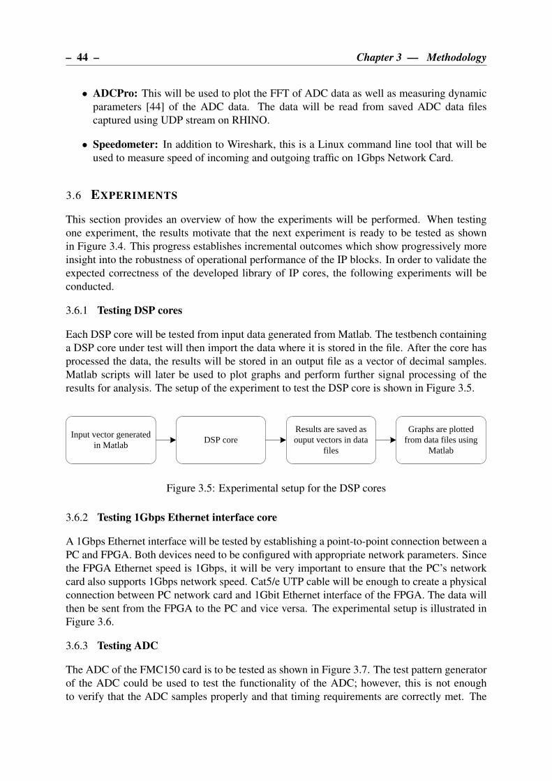
– 44 – Chapter 3 — Methodology
• ADCPro: This will be used to plot the FFT of ADC data as well as measuring dynamic
parameters [44] of the ADC data. The data will be read from saved ADC data files
captured using UDP stream on RHINO.
• Speedometer: In addition to Wireshark, this is a Linux command line tool that will be
used to measure speed of incoming and outgoing traffic on 1Gbps Network Card.
3.6 EXPERIMENTS
This section provides an overview of how the experiments will be performed. When testing
one experiment, the results motivate that the next experiment is ready to be tested as shown
in Figure 3.4. This progress establishes incremental outcomes which show progressively more
insight into the robustness of operational performance of the IP blocks. In order to validate the
expected correctness of the developed library of IP cores, the following experiments will be
conducted.
3.6.1 Testing DSP cores
Each DSP core will be tested from input data generated from Matlab. The testbench containing
a DSP core under test will then import the data where it is stored in the file. After the core has
processed the data, the results will be stored in an output file as a vector of decimal samples.
Matlab scripts will later be used to plot graphs and perform further signal processing of the
results for analysis. The setup of the experiment to test the DSP core is shown in Figure 3.5.
Input vector generated in Matlab
DSP coreResults are saved as ouput vectors in data
files
Graphs are plotted from data files using
Matlab
Figure 3.5: Experimental setup for the DSP cores
3.6.2 Testing 1Gbps Ethernet interface core
A 1Gbps Ethernet interface will be tested by establishing a point-to-point connection between a
PC and FPGA. Both devices need to be configured with appropriate network parameters. Since
the FPGA Ethernet speed is 1Gbps, it will be very important to ensure that the PC’s network
card also supports 1Gbps network speed. Cat5/e UTP cable will be enough to create a physical
connection between PC network card and 1Gbit Ethernet interface of the FPGA. The data will
then be sent from the FPGA to the PC and vice versa. The experimental setup is illustrated in
Figure 3.6.
3.6.3 Testing ADC
The ADC of the FMC150 card is to be tested as shown in Figure 3.7. The test pattern generator
of the ADC could be used to test the functionality of the ADC; however, this is not enough
to verify that the ADC samples properly and that timing requirements are correctly met. The
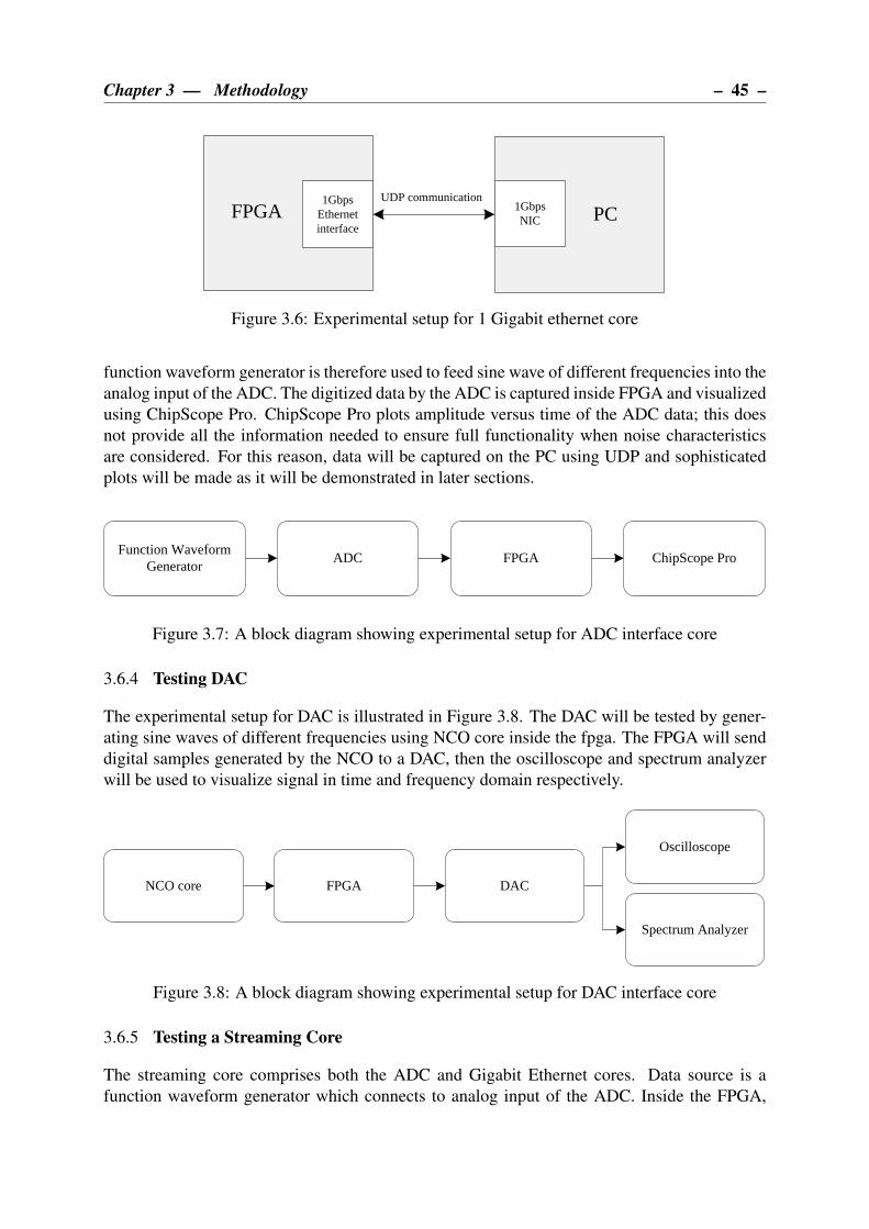
Chapter 3 — Methodology – 45 –
1GbpsEthernet interface
1Gbps NIC
FPGA PCUDP communication
Figure 3.6: Experimental setup for 1 Gigabit ethernet core
function waveform generator is therefore used to feed sine wave of different frequencies into the
analog input of the ADC. The digitized data by the ADC is captured inside FPGA and visualized
using ChipScope Pro. ChipScope Pro plots amplitude versus time of the ADC data; this does
not provide all the information needed to ensure full functionality when noise characteristics
are considered. For this reason, data will be captured on the PC using UDP and sophisticated
plots will be made as it will be demonstrated in later sections.
Function Waveform Generator
ADC FPGA ChipScope Pro
Figure 3.7: A block diagram showing experimental setup for ADC interface core
3.6.4 Testing DAC
The experimental setup for DAC is illustrated in Figure 3.8. The DAC will be tested by gener-
ating sine waves of different frequencies using NCO core inside the fpga. The FPGA will send
digital samples generated by the NCO to a DAC, then the oscilloscope and spectrum analyzer
will be used to visualize signal in time and frequency domain respectively.
NCO core FPGA DAC
Oscilloscope
Spectrum Analyzer
Figure 3.8: A block diagram showing experimental setup for DAC interface core
3.6.5 Testing a Streaming Core
The streaming core comprises both the ADC and Gigabit Ethernet cores. Data source is a
function waveform generator which connects to analog input of the ADC. Inside the FPGA,
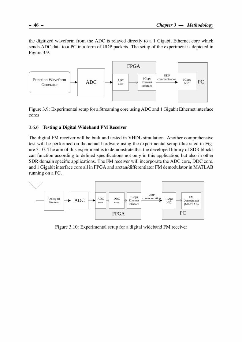
– 46 – Chapter 3 — Methodology
the digitized waveform from the ADC is relayed directly to a 1 Gigabit Ethernet core which
sends ADC data to a PC in a form of UDP packets. The setup of the experiment is depicted in
Figure 3.9.
1GbpsEthernet interface
1Gbps NIC
FPGA
PCUDP
communicationADCFunction Waveform
GeneratorADC core
Figure 3.9: Experimental setup for a Streaming core using ADC and 1 Gigabit Ethernet interface
cores
3.6.6 Testing a Digital Wideband FM Receiver
The digital FM receiver will be built and tested in VHDL simulation. Another comprehensive
test will be performed on the actual hardware using the experimental setup illustrated in Fig-
ure 3.10. The aim of this experiment is to demonstrate that the developed library of SDR blocks
can function according to defined specifications not only in this application, but also in other
SDR domain specific applications. The FM receiver will incorporate the ADC core, DDC core,
and 1 Gigabit interface core all in FPGA and arctan/differentiator FM demodulator in MATLAB
running on a PC.
1GbpsEthernet interface
1Gbps NIC
FPGA PC
UDP communicationADCAnalog RF
FrontendDDC core
ADC core
FM Demodulator(MATLAB )
Figure 3.10: Experimental setup for a digital wideband FM receiver

CHAPTER 4
DESIGN OF SDR DSP BLOCKS
In this chapter the library of FPGA-based DSP blocks is designed. The blocks can also be
referred to as the cores. Where the core or block is a standalone FPGA entity with inputs and
outputs. It is synchronized and controlled by a clock and reset respectively. In order to connect
a core to a standard communication bus, a bus interface functionality is required [18]. The
combination of a core and the bus interface added to it is IP core as illustrated in Figure 4.1.
IP CORECORE
Input ports
Outputports
clock reset
Interface with Bus
Figure 4.1: A block diagram differentiating a Core and IP Core
The designed library of DSP IP cores encompasses the FIR IP core, IIR IP core, FFT/IFFT IP
core and DDC IP core. Each core has a description of a Wishbone interface to show how it can
be attached to Wishbone bus in a SoC design. The goals of implementing these IP cores are
to reduce complexity, increase design reuse, simplify effort of integration and ensure accurate
communication and timing needs.
Figure 4.2 illustrates a general high level architecture of each IP core. It consists of a wishbone
connection and a high-speed I/O connection. The wishbone control logic manages read-write
operations of the slave registers while the FIFO memory stores incoming input data and outgo-
ing processed data.
The FIR IP core will be designed first, then an IIR IP Core, followed by FFT/IFFT IP Core and
lastly DDC IP Core.
4.1 FIR IP CORE
This section presents the design of FIR IP core. The FIR IP core is the FPGA implementation of
FIR filter described in section 2.7.1.1. The design of the filter enables modularity and scalability
47
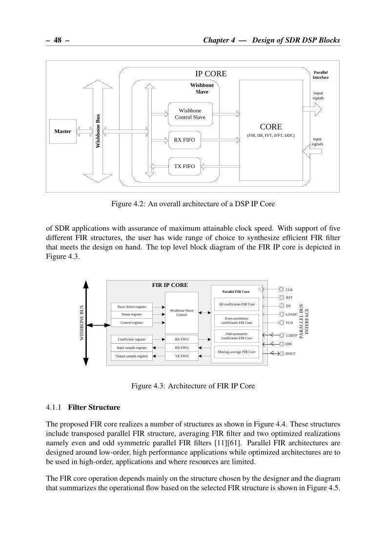
– 48 – Chapter 4 — Design of SDR DSP Blocks
RX FIFO
TX FIFO
CORE(FIR, IIR, FFT, IFFT, DDC)
Wis
hbon
e B
us
Wishbone Slave
Master
IP CORE
ouput signals
input signals
Wishbone Control Slave
Parallel Interface
Figure 4.2: An overall architecture of a DSP IP Core
of SDR applications with assurance of maximum attainable clock speed. With support of five
different FIR structures, the user has wide range of choice to synthesize efficient FIR filter
that meets the design on hand. The top level block diagram of the FIR IP core is depicted in
Figure 4.3.
All coefficients FIR Core
Even-symmetric coefficients FIR Core
Odd-symmetric coefficients FIR Core
Moving-average FIR Core
Parallel FIR Core
TX FIFO
RX FIFO
Coefficient register
Input sample register
Output sample register
Control register
RX FIFO
Status registerWishbone Slave
Control
Slave Select register
CLK
RST
EN
LOADC
VLD
COEFF
DIN
DOUT
FIR IP CORE
WIS
HB
ON
E B
US
n
n
n
PA
RA
LLE
L B
US
IN
TE
RF
AC
E
Figure 4.3: Architecture of FIR IP Core
4.1.1 Filter Structure
The proposed FIR core realizes a number of structures as shown in Figure 4.4. These structures
include transposed parallel FIR structure, averaging FIR filter and two optimized realizations
namely even and odd symmetric parallel FIR filters [11][61]. Parallel FIR architectures are
designed around low-order, high performance applications while optimized architectures are to
be used in high-order, applications and where resources are limited.
The FIR core operation depends mainly on the structure chosen by the designer and the diagram
that summarizes the operational flow based on the selected FIR structure is shown in Figure 4.5.

Chapter 4 — Design of SDR DSP Blocks – 49 –
Z-1 Z-1 Z-1
Z-1 Z-1 Z-1
+ + +
+ + +
x[n]
y[n]
h[n] h[1] h[N/2-2] h[N/2-1]
Even symmetric coefficients FIR filterZ-1 Z-1 Z-1
Z-1 Z-1 Z-1
+ + +
+ + +
x[n]
y[n]h[n] h[1] h[(N-1)/2-1] h[(N-1)/2]
Z-1
Odd symmetric coefficients FIR filter
Z-1 Z-1 Z-1+ +
x[n]
h[N-1] h[N-2] h[1]
+
h[0]
y[n]
Transpose form FIR filter
+ +
x[n]
+y[n]
Z-1 Z-1 Z-1
h
Moving Average FIR filter
Figure 4.4: Parallel FIR structures
Except for a moving FIR filter, the other filter structures use coefficients stored in the ROM or
rather load coefficients from external source. It is the user choice to decide whether to use ROM
coefficients or the externally load them. The FIR core does not begin filtering process until the
coefficients loading is finished. If internal coefficients are used, filtering occurs immediately
without waiting for loading to happen.
Is FIR structure a Moving
Average?
FIR core initializes
Choose FIR structure type
What is filter
coefficients source?
Initialize coefficient iterator : i = 0
Load coefficient sample
i ?
Increment iterator : i = i + 1
Perform FIR filtering
Is FIR output sample
available?
Output the result
Filter still enabled?
Stop FIR filtering
M=number_of_coeffs (Transpose filter)
M=number_of_coeffs/2(Odd-symmetric filter)
M=ceil(number_of_coeffs/2)(Even-symmetric filter)
i < M-1
Internal ROM
External Source
Yes
No
Yes
No
YesNo
i = M - 1
Figure 4.5: FIR core data flow diagram
4.1.2 Filter Coefficients Generation
The FIR core uses fixed point arithmetic to represent data. Using the windowing and iterative
methods discussed in section 2.7.1.1, the coefficients of FIR core are created. However, the
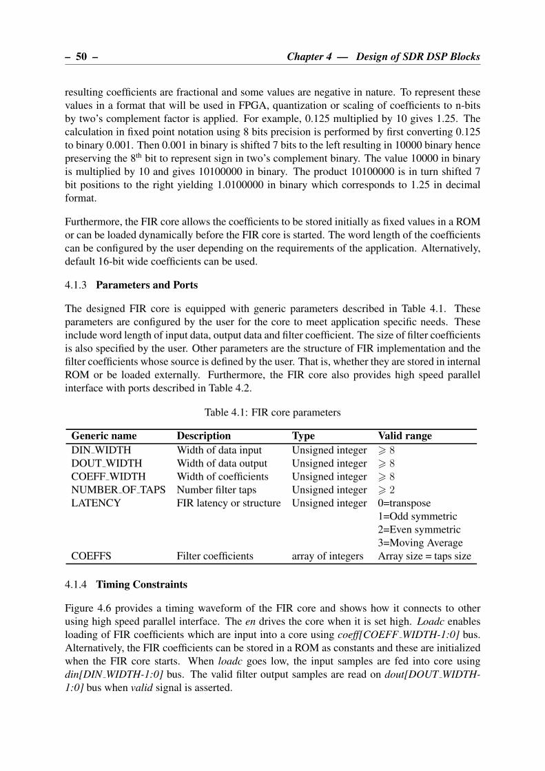
– 50 – Chapter 4 — Design of SDR DSP Blocks
resulting coefficients are fractional and some values are negative in nature. To represent these
values in a format that will be used in FPGA, quantization or scaling of coefficients to n-bits
by two’s complement factor is applied. For example, 0.125 multiplied by 10 gives 1.25. The
calculation in fixed point notation using 8 bits precision is performed by first converting 0.125
to binary 0.001. Then 0.001 in binary is shifted 7 bits to the left resulting in 10000 binary hence
preserving the 8th bit to represent sign in two’s complement binary. The value 10000 in binary
is multiplied by 10 and gives 10100000 in binary. The product 10100000 is in turn shifted 7
bit positions to the right yielding 1.0100000 in binary which corresponds to 1.25 in decimal
format.
Furthermore, the FIR core allows the coefficients to be stored initially as fixed values in a ROM
or can be loaded dynamically before the FIR core is started. The word length of the coefficients
can be configured by the user depending on the requirements of the application. Alternatively,
default 16-bit wide coefficients can be used.
4.1.3 Parameters and Ports
The designed FIR core is equipped with generic parameters described in Table 4.1. These
parameters are configured by the user for the core to meet application specific needs. These
include word length of input data, output data and filter coefficient. The size of filter coefficients
is also specified by the user. Other parameters are the structure of FIR implementation and the
filter coefficients whose source is defined by the user. That is, whether they are stored in internal
ROM or be loaded externally. Furthermore, the FIR core also provides high speed parallel
interface with ports described in Table 4.2.
Table 4.1: FIR core parameters
Generic name Description Type Valid range
DIN WIDTH Width of data input Unsigned integer > 8DOUT WIDTH Width of data output Unsigned integer > 8COEFF WIDTH Width of coefficients Unsigned integer > 8NUMBER OF TAPS Number filter taps Unsigned integer > 2LATENCY FIR latency or structure Unsigned integer 0=transpose
1=Odd symmetric
2=Even symmetric
3=Moving Average
COEFFS Filter coefficients array of integers Array size = taps size
4.1.4 Timing Constraints
Figure 4.6 provides a timing waveform of the FIR core and shows how it connects to other
using high speed parallel interface. The en drives the core when it is set high. Loadc enables
loading of FIR coefficients which are input into a core using coeff[COEFF WIDTH-1:0] bus.
Alternatively, the FIR coefficients can be stored in a ROM as constants and these are initialized
when the FIR core starts. When loadc goes low, the input samples are fed into core using
din[DIN WIDTH-1:0] bus. The valid filter output samples are read on dout[DOUT WIDTH-
1:0] bus when valid signal is asserted.

Chapter 4 — Design of SDR DSP Blocks – 51 –
Table 4.2: FIR core ports
Pin name I/O Description Active state
clk in System Clock Rising edge
rst in System reset high
en in Clock enable high
loadc in Load coefficient enable high
coeff[COEFF WIDTH-1:0] in coefficient input sample data
vld out Valid output data available high
din[DIN WIDTH-1:0] in Filter input sample data
dout[DOUT WIDTH-1:0] out Filter output sample data
clk
rst
en
loadc
coeff [W-1:0]
vld
din [W-1:0]
dout [W-1:0]
data
Δt = number_of_taps × Tclk
Δt = Nout × Tclk
Tclk=10ns
Δt = Nin × Tclk
data
data
Figure 4.6: FIR core input/output timing waveform
4.1.5 Wishbone Interface
Figure 4.7 shows the FIR core connected to a Wishbone slave to enable SoC integration. The
Wishbone interface is composed of high speed parallel ports and wishbone ports. Wishbone
ports are described in section 2.12 and the clk, rst and en ports work the same way as described
in Table 4.2. The ouput ports of the FIR slave provide the FIR core with the input data so that
the FIR core can perform FIR filtering. These include slave dout[15:0] port which sends FIR
input data to a din[15:0] port of the FIR core. Coefficient sample is sent to the FIR core input
using the signal connecting coeff[15:0] ports on both the FIR slave and FIR core. This only
takes place when the FIR core is configured to use external coefficients. Setting slave start/en
signal initiates FIR core filtering process.
The structure in Figure 4.7 also consists of feedback signals from the FIR core to the FIR slave
interface core. Using dout[31:0] port which connects to din[31:0] port of a slave, the FIR core
sends filtered data to slave interface. This happens each time when the vld/en signal is asserted.
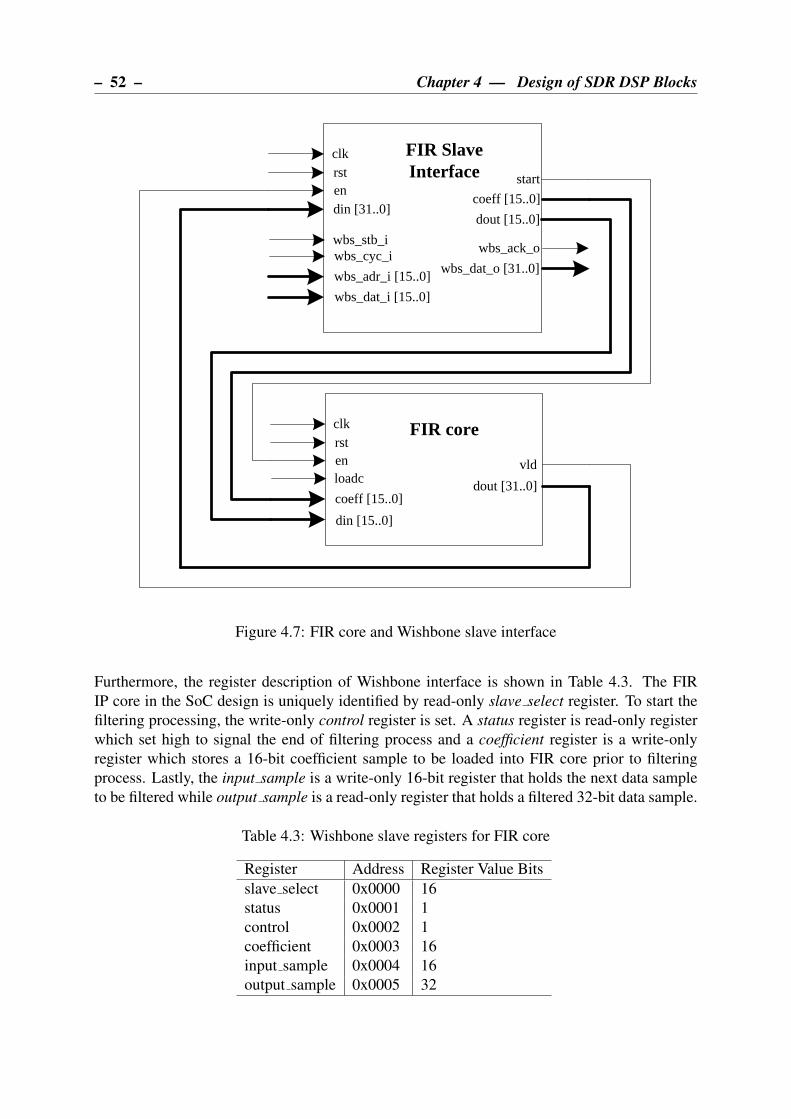
– 52 – Chapter 4 — Design of SDR DSP Blocks
clkrsten
start
FIR Slave Interface
dout [15..0]
wbs_stb_iwbs_cyc_i
wbs_adr_i [15..0]
wbs_dat_i [15..0]
din [31..0]
wbs_ack_o
wbs_dat_o [31..0]
clkrsten
din [15..0]
vld
FIR core
dout [31..0]loadc
coeff [15..0]
coeff [15..0]
Figure 4.7: FIR core and Wishbone slave interface
Furthermore, the register description of Wishbone interface is shown in Table 4.3. The FIR
IP core in the SoC design is uniquely identified by read-only slave select register. To start the
filtering processing, the write-only control register is set. A status register is read-only register
which set high to signal the end of filtering process and a coefficient register is a write-only
register which stores a 16-bit coefficient sample to be loaded into FIR core prior to filtering
process. Lastly, the input sample is a write-only 16-bit register that holds the next data sample
to be filtered while output sample is a read-only register that holds a filtered 32-bit data sample.
Table 4.3: Wishbone slave registers for FIR core
Register Address Register Value Bits
slave select 0x0000 16
status 0x0001 1
control 0x0002 1
coefficient 0x0003 16
input sample 0x0004 16
output sample 0x0005 32
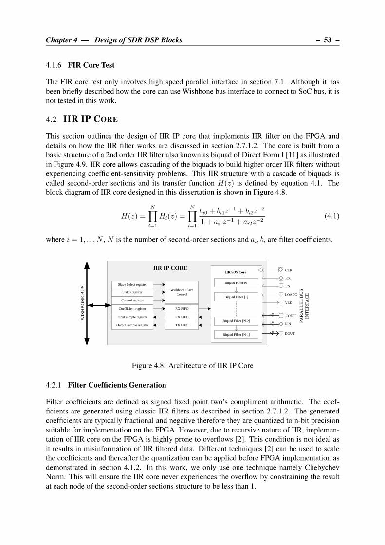
Chapter 4 — Design of SDR DSP Blocks – 53 –
4.1.6 FIR Core Test
The FIR core test only involves high speed parallel interface in section 7.1. Although it has
been briefly described how the core can use Wishbone bus interface to connect to SoC bus, it is
not tested in this work.
4.2 IIR IP CORE
This section outlines the design of IIR IP core that implements IIR filter on the FPGA and
details on how the IIR filter works are discussed in section 2.7.1.2. The core is built from a
basic structure of a 2nd order IIR filter also known as biquad of Direct Form I [11] as illustrated
in Figure 4.9. IIR core allows cascading of the biquads to build higher order IIR filters without
experiencing coefficient-sensitivity problems. This IIR structure with a cascade of biquads is
called second-order sections and its transfer function H(z) is defined by equation 4.1. The
block diagram of IIR core designed in this dissertation is shown in Figure 4.8.
H(z) =N∏
i=1
Hi(z) =N∏
i=1
bi0 + bi1z−1 + bi2z
−2
1 + ai1z−1 + ai2z−2(4.1)
where i = 1, ..., N , N is the number of second-order sections and ai, bi are filter coefficients.
Biquad Filter [0]
IIR SOS Core
TX FIFO
RX FIFO
Coefficient register
Input sample register
Output sample register
Control register
RX FIFO
Status registerWishbone Slave
Control
Slave Select register
CLK
RST
EN
LOADC
VLD
COEFF
DIN
DOUT
IIR IP CORE
WIS
HB
ON
E B
US
Biquad Filter [1]
Biquad Filter [N-1]
Biquad Filter [N-2]
n
n
n
PA
RA
LLE
L B
US
IN
TE
RF
AC
E
Figure 4.8: Architecture of IIR IP Core
4.2.1 Filter Coefficients Generation
Filter coefficients are defined as signed fixed point two’s compliment arithmetic. The coef-
ficients are generated using classic IIR filters as described in section 2.7.1.2. The generated
coefficients are typically fractional and negative therefore they are quantized to n-bit precision
suitable for implementation on the FPGA. However, due to recursive nature of IIR, implemen-
tation of IIR core on the FPGA is highly prone to overflows [2]. This condition is not ideal as
it results in misinformation of IIR filtered data. Different techniques [2] can be used to scale
the coefficients and thereafter the quantization can be applied before FPGA implementation as
demonstrated in section 4.1.2. In this work, we only use one technique namely Chebychev
Norm. This will ensure the IIR core never experiences the overflow by constraining the result
at each node of the second-order sections structure to be less than 1.

– 54 – Chapter 4 — Design of SDR DSP Blocks
Z-1
+
x[n]
b1
Z-1
Z-1
Z-1
+
+y[n]
b2
b0
-a1
-a2
Z-1
+
x[n]
b1
Z-1
Z-1
Z-1
+
+y[n]
b2
b0
-a1
-a2
Biquad [0] Biquad [N-1]Biquad[1] . . . Biquad[N-2]
. . .
IIR SOS Filter
Figure 4.9: Cascaded Direct Form I Biquad IIR filter
Furthermore, a Matlab script that can be used to quickly and easily scale the IIR filter coeffi-
cients is found in Appendix C.2. It uses Chebychev Norm (Infinity-Norm) l∞ = maxω
|G(ω)|,where G(w) is unscaled filter frequency response. The scaling procedure used in this design is
described in [2, 86]. This is based on estimation of scaling factors si = 1/li∞ which provide
maximum amplitudes in biquad stages yi but prevent the output adders from overflow at ith
stage of second-order sections structure. The cascaded frequency reponses G0i(z) have to be
DFI1 DFI2 DFI3 DFI4 DFI5 DFI6
G01(z)
G02(z)
G03(z)
G04(z)
G05(z)
G06(z)
G1s(z) = s1G1(z) G2s(z) = s2G2(z) G3s(z) = s3G3(z) G4s(z) = s4G4(z) G5s(z) = s5G5(z) G6s(z) = s6G6(z)
x(n) y(n)
Figure 4.10: Six Cascaded second-order sections (DFI=Direct Form I)
regarded because separate scaling of Gi(z) will cause decreasing magnitudes from one second-
order section stage to the next [86]. The example below shows how scaling is performed for six
cascaded second-order sections of direct form I illustrated in Figure 4.10.
• The scaled frequency response at ith stage is
Gis(z) = siGi(z)
• Scale factor si ensures that the overall gain of the filter from input x[n] to output yi is
unity to avoid overflow.
• Notation: to find infinity-norm for some transfer function G(z), we use
l-norm of Gi(z) = maxω
|G(ω)| = l∞(Gi(z)) = lGi

Chapter 4 — Design of SDR DSP Blocks – 55 –
• Calculate the Chebychev Norm of cascaded frequency response:
lG01= l∞(G01(z)) = l∞(G1)
lG02= l∞(G02(z)) = l∞(s1G1(z)G2(z)) = s1l∞(G1G2(z))
lG03= l∞(G03(z)) = l∞(s1s2G1(z)G2(z)G3(z)) = s1s2l∞(G1(z)G2(z)G3(z))
lG04= l∞(G04(z)) = l∞(s1s2s3G1(z)G2(z)G3(z)G4(z))
= s1s2s3l∞(G1(z)G2(z)G3(z)G4(z))
lG05= l∞(G05(z)) = l∞(s1s2s3s4G1(z)G2(z)G3(z)G4(z)G5(z))
= s1s2s3s4l∞(G1(z)G2(z)G3(z)G4(z)G5(z))
lG06= l∞(G06(z)) = l∞(s1s2s3s4s5G1(z)G2(z)G3(z)G4(z)G5(z)G6(z))
= s1s2s3s4s5l∞(G1(z)G2(z)G3(z)G4(z)G5(z)G6(z))
• Using si = 1/li∞ and the previous equations for Chebychev Norm at each stage, we
obtain the scaling factors as below:
s1 = 1/lG01
= 1/l∞(G1(z))
s2 = 1/lG02
= 1/(s1l∞(G1G2(z)))
s3 = 1/lG03
= 1/(s1s2l∞(G1(z)G2(z)G3(z)))
s4 = 1/lG04
= 1/(s1s2s3l∞(G1(z)G2(z)G3(z)G4(z)))
s5 = 1/lG05
= 1/(s1s2s3s4l∞(G1(z)G2(z)G3(z)G4(z)G5(z)))
s6 = 1/lG06
= 1/(s1s2s3s4s5l∞(G1(z)G2(z)G3(z)G4(z)G5(z)G6(z)))
• s1s2s3s4s5s6 = 1, because of the original gain of the full order l∞(G(ω)) = l∞(G1G2G3G4G5G6) =1 description.
• Finally, scaling coefficients is performed:
s1 : b01s = s1 × b01, b11s = s1 × b11, b21s = s1 × b21s2 : b02s = s2 × b02, b12s = s1 × b12, b22s = s1 × b22s3 : b03s = s3 × b03, b13s = s3 × b13, b23s = s3 × b23s4 : b04s = s4 × b04, b14s = s4 × b14, b24s = s4 × b24s5 : b05s = s5 × b05, b15s = s5 × b15, b25s = s5 × b25s6 : b06s = s6 × b06, b16s = s6 × b16, b26s = s6 × b26
4.2.2 Parameters and Ports
The IIR core is composed of generic parameters which are configurable by user. These are
described in Table 4.4. The parameters include the word length of input data, output data and
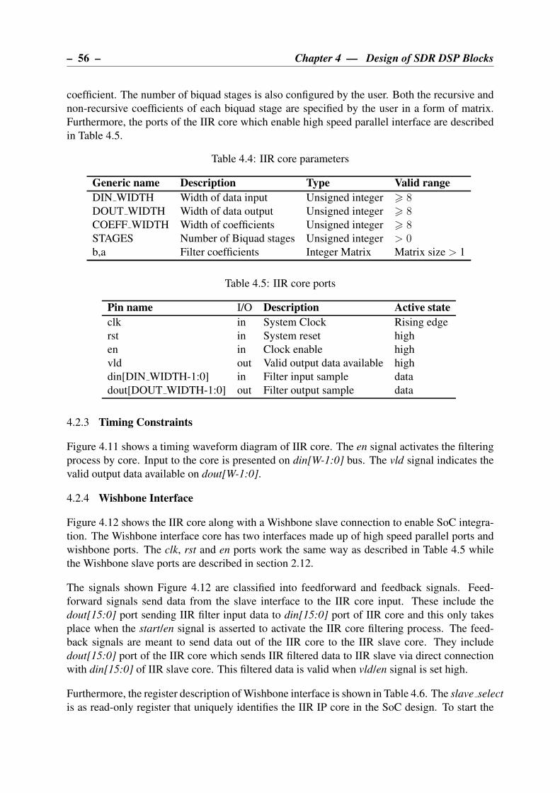
– 56 – Chapter 4 — Design of SDR DSP Blocks
coefficient. The number of biquad stages is also configured by the user. Both the recursive and
non-recursive coefficients of each biquad stage are specified by the user in a form of matrix.
Furthermore, the ports of the IIR core which enable high speed parallel interface are described
in Table 4.5.
Table 4.4: IIR core parameters
Generic name Description Type Valid range
DIN WIDTH Width of data input Unsigned integer > 8DOUT WIDTH Width of data output Unsigned integer > 8COEFF WIDTH Width of coefficients Unsigned integer > 8STAGES Number of Biquad stages Unsigned integer > 0b,a Filter coefficients Integer Matrix Matrix size > 1
Table 4.5: IIR core ports
Pin name I/O Description Active state
clk in System Clock Rising edge
rst in System reset high
en in Clock enable high
vld out Valid output data available high
din[DIN WIDTH-1:0] in Filter input sample data
dout[DOUT WIDTH-1:0] out Filter output sample data
4.2.3 Timing Constraints
Figure 4.11 shows a timing waveform diagram of IIR core. The en signal activates the filtering
process by core. Input to the core is presented on din[W-1:0] bus. The vld signal indicates the
valid output data available on dout[W-1:0].
4.2.4 Wishbone Interface
Figure 4.12 shows the IIR core along with a Wishbone slave connection to enable SoC integra-
tion. The Wishbone interface core has two interfaces made up of high speed parallel ports and
wishbone ports. The clk, rst and en ports work the same way as described in Table 4.5 while
the Wishbone slave ports are described in section 2.12.
The signals shown Figure 4.12 are classified into feedforward and feedback signals. Feed-
forward signals send data from the slave interface to the IIR core input. These include the
dout[15:0] port sending IIR filter input data to din[15:0] port of IIR core and this only takes
place when the start/en signal is asserted to activate the IIR core filtering process. The feed-
back signals are meant to send data out of the IIR core to the IIR slave core. They include
dout[15:0] port of the IIR core which sends IIR filtered data to IIR slave via direct connection
with din[15:0] of IIR slave core. This filtered data is valid when vld/en signal is set high.
Furthermore, the register description of Wishbone interface is shown in Table 4.6. The slave select
is as read-only register that uniquely identifies the IIR IP core in the SoC design. To start the

Chapter 4 — Design of SDR DSP Blocks – 57 –
clk
rst
en
vld
din [W-1:0]
dout [W-1:0]
data
Δt = Nout × Tclk
Tclk=10ns
Δt = Nin × Tclk
data
Figure 4.11: IIR core input/output timing waveform
filtering processing, the write-only control register is set. A status register is read-only register
which set high to signal the end of filtering process, and lastly the input sample is a write-
only 16-bit register of to hold data the next data sample to be filtered while output sample is a
read-only register that keeps a filtered 32-bit data sample.
Table 4.6: Wishbone slave registers for IIR core
Register Address Register Value Bits
slave select 0x0000 16
status 0x0001 1
control 0x0002 1
input sample 0x0003 16
output sample 0x0004 32
4.2.5 IIR core Test
Testing of IIR core is based on parallel interface in section 7.2 and Wishbone bus testing is not
discussed.
4.3 FFT/IFFT IP CORE
This section present the design of an IP core to perform FFT computation and FFT literature
is discussed in section 2.7.2. Fast Fourier Transform (FFT) is an efficient implementation of
Discrete Fourier Transform (DFT). The function of a DFT is to map time domain data sequence
into frequency domain data sequence [73]. FFT output X[k] is defined by the equation 4.2.
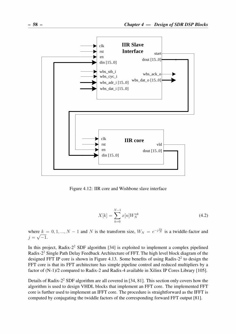
– 58 – Chapter 4 — Design of SDR DSP Blocks
clkrsten
start
IIR Slave Interface
dout [15..0]
wbs_stb_iwbs_cyc_i
wbs_adr_i [15..0]
wbs_dat_i [15..0]
din [15..0]
wbs_ack_o
wbs_dat_o [15..0]
clkrstendin [15..0]
vldIIR core
dout [15..0]
Figure 4.12: IIR core and Wishbone slave interface
X[k] =N−1∑
k=0
x[n]W nkN (4.2)
where k = 0, 1, ..., N − 1 and N is the transform size, WN = e−j 2πN is a twiddle-factor and
j =√−1.
In this project, Radix-22 SDF algorithm [34] is exploited to implement a complex pipelined
Radix-22 Single Path Delay Feedback Architecture of FFT. The high level block diagram of the
designed FFT IP core is shown in Figure 4.13. Some benefits of using Radix-22 to design the
FFT core is that its FFT architecture has simple pipeline control and reduced multipliers by a
factor of (N-1)/2 compared to Radix-2 and Radix-4 available in Xilinx IP Cores Library [105].
Details of Radix-22 SDF algorithm are all covered in [34, 81]. This section only covers how the
algorithm is used to design VHDL blocks that implement an FFT core. The implemented FFT
core is further used to implement an IFFT core. The procedure is straightforward as the IFFT is
computed by conjugating the twiddle factors of the corresponding forward FFT output [81].

Chapter 4 — Design of SDR DSP Blocks – 59 –
The FFT Core length is configured to be 4, 816, 32, 64, 128, 256, 512, 1024, 2048 and 4096.
However, larger size FFTs can be also be achieved by following guidelines outlined in sec-
tion 4.3.3. The designed core is meant to be used and applied in fields where SDR is prevalent
such as digital communication systems, radar systems and multimedia systems.
FFT - 23
Radix-22 SDF FFT Core
TX FIFO
RX FIFOInput sample register
Output sample register
Control register
Status register
Wishbone Slave Control
Slave Select register
CLK
RST
EN
VLD
XSr
XSi
XKi
Radix-22 SDF FFT IP CORE
WIS
HB
ON
E B
US
FFT - 24
FFT – 2N
FFT – 2N-1
. . .
XKr
PA
RA
LLE
L B
US
IN
TE
RF
AC
E
n
n
n
n
Figure 4.13: The architecture of FFT IP Core
4.3.1 Design Structure
A typical Radix-22 SDF FFT is illustrated in Figure 4.14. In this particular design data arrives
at the input in a natural order and outputs results in a bit-reversed sequence. For an FFT with
N points, a complete stage consists of two butterflies namely BFI and BFII, delay feedback
shift register and a twiddle factor complex multiplier. On the other hand, half a stage only has a
single butterfly which is BFI whereas the important formulas used to determine specific number
of building blocks in the FFT architecture are clearly described in Table 4.7. The building blocks
of the architecture are described below.
Table 4.7: The description of formulas used for FFT architecture
Formula Description
N Number of FFT points
N − 1 Number of registers found in feedback registers
log4(N) Number of stages
log2(N) Number of butterflies and shift registers
2log2(N) Number of adders
log2(N)−1
2Number of complex multipliers
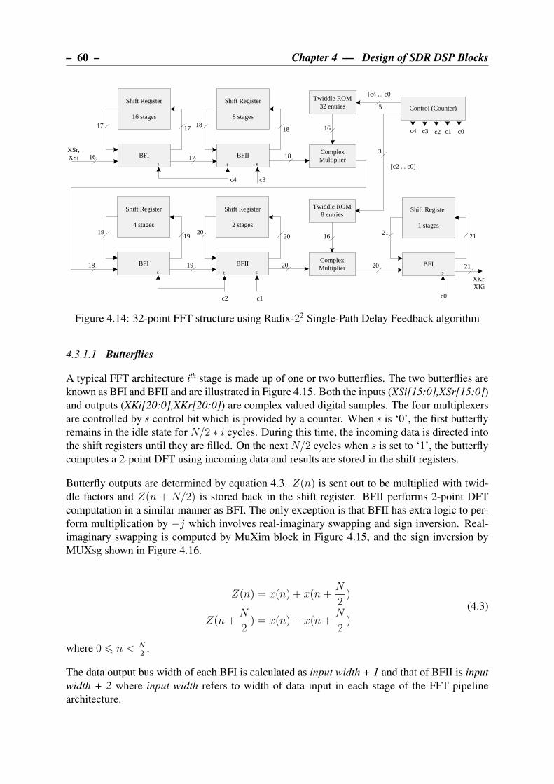
– 60 – Chapter 4 — Design of SDR DSP Blocks
Shift Register
16 stages
BFIs
16
1717
Shift Register
8 stages
BFIIs
17
1818
Complex Multiplier
Twiddle ROM32 entries
16
Shift Register
4 stages
BFIs
18
1919
Shift Register
2 stages
BFIIs
19
2020
Complex Multiplier
Twiddle ROM8 entries
16
[c2 ... c0]
Shift Register
1 stages
BFIs
20
21
t
t
Control (Counter)
c0
[c4 ... c0]
c1c2c3
c0c1c2
c4
c3c4
3
5
18
20
21
21
XSr, XSi
XKr, XKi
Figure 4.14: 32-point FFT structure using Radix-22 Single-Path Delay Feedback algorithm
4.3.1.1 Butterflies
A typical FFT architecture ith stage is made up of one or two butterflies. The two butterflies are
known as BFI and BFII and are illustrated in Figure 4.15. Both the inputs (XSi[15:0],XSr[15:0])
and outputs (XKi[20:0],XKr[20:0]) are complex valued digital samples. The four multiplexers
are controlled by s control bit which is provided by a counter. When s is ‘0’, the first butterfly
remains in the idle state for N/2 ∗ i cycles. During this time, the incoming data is directed into
the shift registers until they are filled. On the next N/2 cycles when s is set to ‘1’, the butterfly
computes a 2-point DFT using incoming data and results are stored in the shift registers.
Butterfly outputs are determined by equation 4.3. Z(n) is sent out to be multiplied with twid-
dle factors and Z(n + N/2) is stored back in the shift register. BFII performs 2-point DFT
computation in a similar manner as BFI. The only exception is that BFII has extra logic to per-
form multiplication by −j which involves real-imaginary swapping and sign inversion. Real-
imaginary swapping is computed by MuXim block in Figure 4.15, and the sign inversion by
MUXsg shown in Figure 4.16.
Z(n) = x(n) + x(n+N
2)
Z(n+N
2) = x(n)− x(n+
N
2)
(4.3)
where 0 6 n < N2
.
The data output bus width of each BFI is calculated as input width + 1 and that of BFII is input
width + 2 where input width refers to width of data input in each stage of the FFT pipeline
architecture.
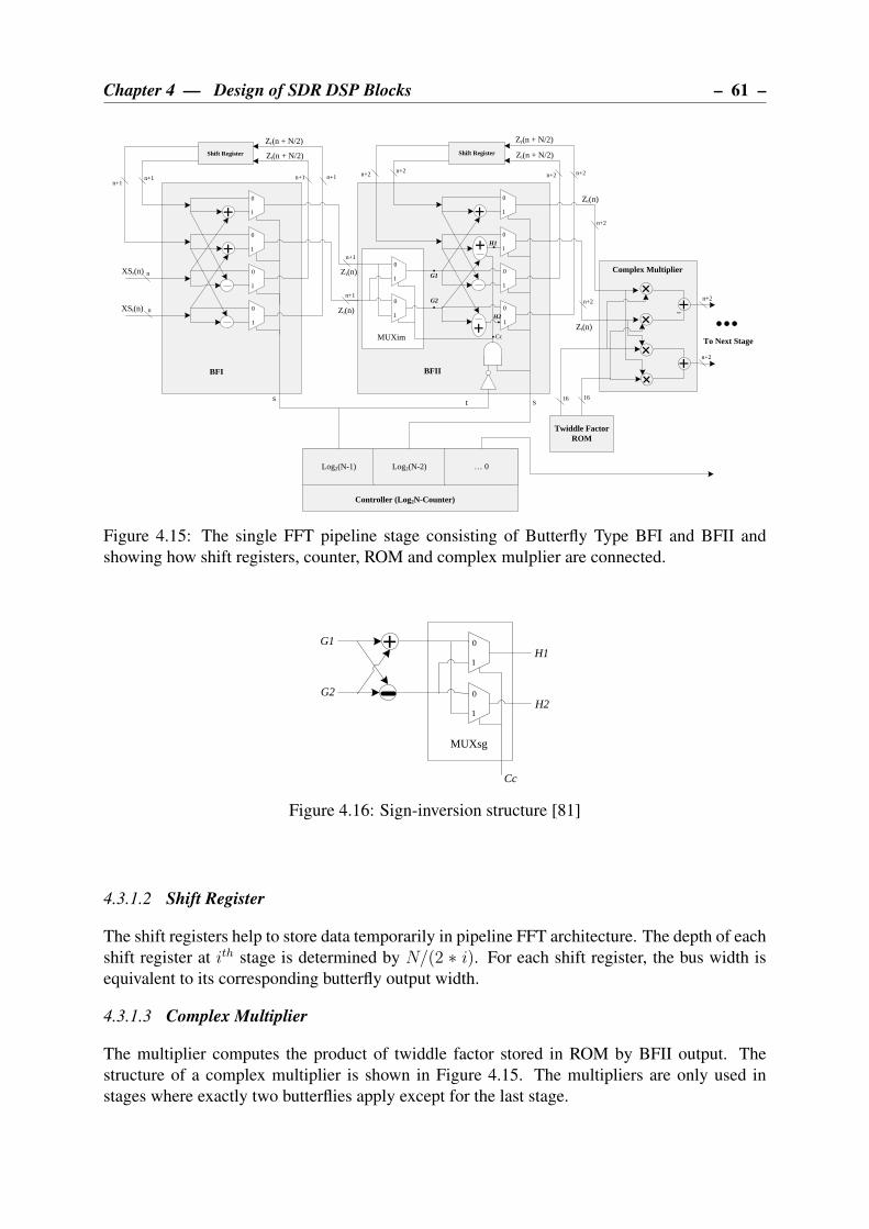
Chapter 4 — Design of SDR DSP Blocks – 61 –
Shift Register
+
+
0
1
0
1
0
1
0
1
XSr(n)
XSi(n)
Zr(n)
Zi(n)
Zr(n + N/2)
Zi(n + N/2)
s
Shift Register
+0
1
0
1
0
1
0
1
Zr(n)
Zi(n)
Zr(n + N/2)
Zi(n + N/2)
s
0
1
0
1
H1
H2
G1
G2
.
..
.
t
MUXim
+
+
Cc.
BFI BFII
+
+
+
+
+
+
_
Twiddle Factor ROM
Log2(N-1) Log2(N-2) … 0
Controller (Log2N-Counter)
Complex Multiplier
To Next Stage
...n
n
n+1
n+1
n+1n+1n+1n+1
n+2n+2n+2n+2
n+2
n+2
1616
n+2
n+2
Figure 4.15: The single FFT pipeline stage consisting of Butterfly Type BFI and BFII and
showing how shift registers, counter, ROM and complex mulplier are connected.
G1
G2
0
1
0
1
MUXsg
+H1
H2
Cc
Figure 4.16: Sign-inversion structure [81]
4.3.1.2 Shift Register
The shift registers help to store data temporarily in pipeline FFT architecture. The depth of each
shift register at ith stage is determined by N/(2 ∗ i). For each shift register, the bus width is
equivalent to its corresponding butterfly output width.
4.3.1.3 Complex Multiplier
The multiplier computes the product of twiddle factor stored in ROM by BFII output. The
structure of a complex multiplier is shown in Figure 4.15. The multipliers are only used in
stages where exactly two butterflies apply except for the last stage.

– 62 – Chapter 4 — Design of SDR DSP Blocks
4.3.1.4 Twiddle Factor ROM
Every complete stage of Radix-22 FFT architecture requires that a twiddle factor be multiplied
with BFII output. The twiddle factors are constant complex values stored in 16-bit ROM with
depth of N/22i at each ith stage. These twiddle factors are generated according to equation 4.4
and then stored in ROM. Using MATLAB script provided in Appendix D.4, the ROM HDL files
containing twiddle factors can be generated easily. The appropriate twiddle factor is selected by
control logic in the pipeline structure. Each ROM is addressed by a sliced vector of bits from
control logic as shown in Figure 4.14. The vector slice is in a form of log2
(
N22i
)
. The twiddle
factor at ith-stage, with i = 0, 1, ..., (log4N) − 2 is given by Wi = ux ; x = 0, 1, ..., N22i
with
ux = e−j2πv
N
v =
0, 0 6 x < a22i+1 × (x− a), a 6 x < 2a22i × (x− 2a), 2a 6 x < 3a
3× 22i × (x− 3a), 3a 6 x < 4a
(4.4)
where a = N22+2i [81] .
4.3.1.5 Controller
The control logic of a Radix-22 FFT pipeline is implemented with a simple digital log2(N)-bit
counter. The counter is used to control the butterfly multiplexers, thus enabling the butterflies to
switch between operating modes described in section 4.3.1.1. Furthermore, the counter is used
to address Twiddle Factor ROM which directs its output to a complex multiplier in each stage
of the FFT.
4.3.2 Parameters and Ports
The FFT/IFFT core consists of generic parameters which make it possible for user to customize
its functionality depending on the application needs. These parameters are described in Ta-
ble 4.8. The parameters include the word length of the input data, output data and twiddle
factor stored in ROM. The core also enables the number of FFT points to be specified by the
user. Furthermore, the ports on the FFT/IFFT core enable connection to other cores using high
speed parallel interface as described in Table 4.9.
Table 4.8: FFT core parameters
Generic name Description Type Valid Range
N Number of FFT points unsigned integer 8, 16, 32, 64, 128, 256,
512, 1024, 2048, 4096
DIN WIDTH Bit width of input samples unsigned integer 8 to 32
DOUT WIDTH Bit width of input samples unsigned integer 8 to 32
TF WIDTH Bit width of twiddle factors unsigned integer > 8, default=16

Chapter 4 — Design of SDR DSP Blocks – 63 –
Table 4.9: FFT core pin-out
Port name I/O Description Active State
clk in System Clock Rising Edge
rst in System Reset high
en in Clock Enable high
XSr[DIN WIDTH-1:0] in Real-part input sample data
XSi[DIN WIDTH-1:0] in Imaginary-part input sample data
vld out Valid data available high
done out FFT complete high
XKr[DOUT WIDTH-1:0] out Real-part output sample data
XKi[DOUT WIDTH-1:0] out Imaginary-part output sample data
4.3.3 Core Generation Flow for Higher Length FFTs
The designed FFT/IFFT core supports the number of FFT points specified in Table 4.8. How-
ever, a straightforward procedure can be followed to create FFT or IFFT core with more points
than the maximum value of 4096. This same method can be used to generate an FFT structure
of any length greater than or equal to 8 provided the FFT length is a power of two.
Figure 4.17 shows the flow of generation of HDL modules to build the top level design of the
desired FFT or IFFT core by connecting butterfly stages, twiddle factor ROMs and a counter.
Due to the modular structure of the designed FFT/IFFT core, its modules are reused to build
custom FFT/IFFT cores.
As shown in Figure 4.17, the process starts by computing the number of stages using log4N .
All the stages preceding the last stage are built using r22sdf stage.vhd. In each ith stage, there
is Twiddle Factor ROM whose depth is determined by N/22i. The ROM HDL files for FFT
stages are generated using a Matlab script provided in Appendix D.4. Finally, the last stage
is generated based on the FFT length used and it does not have a Twiddle Factor ROM. If the
calculated number of stages is fractional, r22sdf odd last stage.vhd file is used to build the last
stage. If the computed number of the stages is a whole number, the last stage is created using
r22sdf even last stage.vhd file. The controller of the FFT is a simple log2(N)-bit counter which
is implemented in counter.vhd file. The counter has n-bit counting register that is configurable
by the user.
4.3.4 Timing Constraints
A high speed parallel interface to an FFT core is illustrated in Figure 4.18. The core performs
FFT function of N points as long as en remains high. Input digital data is represented in complex
format. XSr[DIN WIDTH-1:0] and XSi[DIN WDTH-1:0] buses are used for input and they
represent real and imaginary data respectively. vld goes high after N-1 input samples to signal
availability of output sample on XKr[DIN WIDTH-1:0] and XKi[DIN WIDTH-1:0] which are
in complex values.
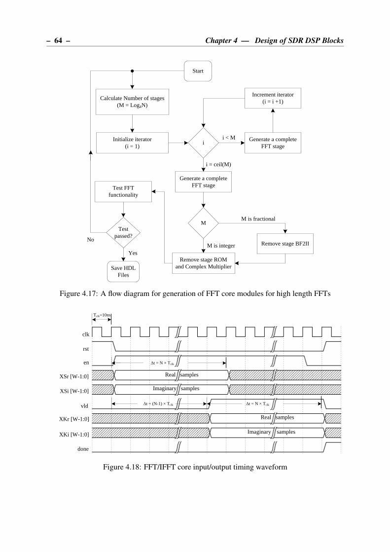
– 64 – Chapter 4 — Design of SDR DSP Blocks
i
Calculate Number of stages (M = Log4N)
Initialize iterator (i = 1)
Generate a complete FFT stage
Increment iterator(i = i +1)
M
i < M
i = ceil(M)
Remove stage ROM and Complex Multiplier
M is integer
M is fractional
Remove stage BF2II
Generate a complete FFT stage
Save HDL Files
Start
Test FFT functionality
Test passed?
Yes
No
Figure 4.17: A flow diagram for generation of FFT core modules for high length FFTs
clk
rst
en
XSr [W-1:0]
XSi [W-1:0]
vld
XKr [W-1:0]
XKi [W-1:0]
done
Real samples
Imaginary samples
Real samples
Imaginary samples
Δt = N × Tclk
Δt = N × TclkΔt = (N-1) × Tclk
Tclk=10ns
Figure 4.18: FFT/IFFT core input/output timing waveform

Chapter 4 — Design of SDR DSP Blocks – 65 –
4.3.5 Wishbone Interface
In order to make an FFT/IFFT core Wishbone compatible, the Wishbone Slave Interface core
is designed and connected to FFT/IFFT core as shown in Figure 4.19. The three control ports
namely clk, rst and en operate as described in Table 4.9 and the Wishbone slave ports are
described in section 2.12. The signals connecting the two blocks are divided into feedforward
and feedback signals. The feedforward signals include the start/en signal which starts the FFT
or IFFT processing on the FFT/IFFT core. Both doutr[15:0] and douti[15:0] ports are real
and imaginary data ports respectively and are used to transfer input samples to corresponding
XSr[15:0] and XSi[15:0] ports of the FFT/IFFT core.
clkrst
enstart
FFT/IFFT Slave Interface
doutr [15..0]
wbs_stb_iwbs_cyc_i
wbs_adr_i [15..0]
wbs_dat_i [31..0]
dinr [15..0]
wbs_ack_o
wbs_dat_o [31..0]
dini [15..0]douti [15..0]
clkrsten
XSi [15..0]
vld
FFT/IFFT core
XKr [15..0]XSr [15..0]
XKi [15..0]
done
stop
Figure 4.19: FFT core and Wishbone slave interface
Additionally, the feedback signal are used by FFT/IFFT core to send output data to slave inter-
face core as shown in Figure 4.19. The data processed by the FFT/IFFT core is sent through
imaginary and real ports namely XKr[15:0] and XKi[15:0] ports which connect directly to
dinr[15:0] and dini[15:0] of the FFT/IFFT slave block. The vld/en signal is set high to enable
output data transfer from one block to another while done/stop signal goes high to indicate that
FFT/IFFT core has completed processing.

– 66 – Chapter 4 — Design of SDR DSP Blocks
Furthermore, the description of FFT/IFFT Wishbone slave registers is described in Table 4.10.
The slave select is a read-only register used to uniquely identify the FFT/IFFT IP core. In order
start the FFT/IFFT core processing, the write-only control register needs to be set. The end of
FFT/IFFT processing is denoted by active high read-only status register. Lastly the write-only
input sample register and read-only output sample register are both used for input and output
data respectively. Their bit precision is 32 bits which is a concatenation of 16-bit real and
imaginary input and output samples.
Table 4.10: Wishbone slave registers for FFT/IFFT core
Register Address Register Value Bits
slave select 0x0000 16
status 0x0001 1
control 0x0002 1
input sample 0x0003 32
output sample 0x0004 32
4.3.6 FFT/IFFT core Test
The FFT/IFFT core test is discussed in section 7.3 using only parallel interface. Wishbone bus
interface testing is not covered in this work.
4.4 DDC IP CORE
This section discusses the design of a DDC IP core. The literature for DDC algorithm is covered
in section 2.7.3. The DDC performs the first processing work after ADC [95] and is used in
applications where frequency down conversion, sample rate reduction and high speed filtering
is required. The developed DDC core is highly configurable and can be tailored easily to meet
many SDR multi-rate applications needs. Figure 4.20 illustrates the top level block diagram of
the DDC IP core.
4.4.1 DDC structure
The DDC architecture is realized as shown in Figure 4.21. The NCO, digital mixer, CIC and
FIR filter were all designed to complete the structure of the DDC as explained below.
4.4.1.1 NCO
The Numerically Controlled Oscillator (NCO) synthesizes discrete-time sine and cosine wave-
forms with a configurable waveform frequency as shown in Figure 4.22. The waveforms are
generated from a lookup table containing a vector of sine and cosine values which are suc-
cessively addressed by the phase accumulator output. The phase step of the accumulator is
determined by Frequency Tuning Word (FTW) calculated using equation 4.5. n represents the
width of phase in bits; fout is the desired frequency of the output waveforms and fclk is the
frequency of the clock.
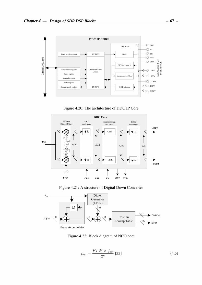
Chapter 4 — Design of SDR DSP Blocks – 67 –
Mixer
Compensating Filter
CIC Decimator
DDC Core
Control register
Status register
Wishbone Slave Control
Slave Select register
CLK
RST
EN
RDY
CLKO
IOUT
QOUT
DDC IP COREW
ISH
BO
NE
BU
S
FTW
VLD
DIN
CIC Decimator 1
PA
RA
LLE
L B
US
IN
TE
RF
AC
E
n
n
n
n
RX FIFOInput sample register
TX FIFOOutput sample register
FTW register
Figure 4.20: The architecture of DDC IP Core
NCO & Digital Mixer
Compensation FIR filter
CIC 1 decimator
DDC Core
LO
CFIRR
R CFIR
R
R
CIC 2 decimator
CLK
DIN
RST ENFTW RDY VLD
IOUT
QOUT
n
900
n
n
nn
n n
n
n
n
x1[n] x2[m] x3[m] x4[k]
n
16
16
Figure 4.21: A structure of Digital Down Converter
D
+ +
Dither Generator(LFSR)
Cos/Sin Lookup Table
n n n
m
16
16
Phase Accumulator
cosine
sineFTW
fclk
Figure 4.22: Block diagram of NCO core
fout =FTW × fclk
2n[33] (4.5)

– 68 – Chapter 4 — Design of SDR DSP Blocks
Due to phase quantization, the spurious harmonics in the NCO waveform output are created.
In order to equally distribute these unwanted harmonics, the random number is generated [21]
using Linear Feedback Shift Register (LSFR) and added to the least significant bits of the phase
accumulator. The process is referred to as phase dithering and it improves effective SFDR of
the NCO-generated waveforms. The NCO of the DDC core has a configurable phase dithering
in order to attain the highest possible SFDR in the output waveforms.
4.4.1.2 Digital Mixer
The digital mixer is used to mix down the RF or IF signal to baseband signal for further pro-
cessing. It takes in the local oscillator signal at IF frequency and multiplies it by an incoming
IF signal. The product of these two signals has both the desired baseband signal and out-of-
band higher order frequency components. Filtering is therefore required in order to isolate a
baseband signal.
4.4.1.3 CIC Decimation filter
The CIC decimation core is designed to reduce the sampling rate in the DDC. It also has a low-
pass filter characteristic which is efficient and cost effective. As a result, it is used to eliminate
noise emanating from a digital mixer. The simplified structure of the CIC decimation filter is
illustrated in Figure 4.23.
++
-
++
-
+ +
Dec
imat
e by
R =
2 to
163
84
... ...
Z-MZ-M
x(n)
fs
N stagesSampling Rate = fs
N stagesSampling Rate = fs/R
y(n)
fs/R
Z-1Z-1 Z-1Z-1
Figure 4.23: Block diagram of a CIC core
The CIC decimator is the chain of N integrator stages and N comb stages. It comprises an
integrator section operating at high sampling rate fs and comb section operating at lower rate
fs/R. These two sections are separated by a decimator which is denoted by R. The combs have
a differential delay M which is used to control the filter’s frequency response [91]. The system
transfer function H(z) and magnitude response |H(f)| are defined by equation 4.6.
Chapter 4 — Design of SDR DSP Blocks – 69 –
H(z) =(1− z−RM)N
(1− z−1)N
=
[
RM−1∑
k=0
z−k
]N
|H(f)| =∣
∣
∣
∣
∣
sin(πMf)
sin(πfR)
∣
∣
∣
∣
∣
N
[91]
(4.6)
where a complex variable z = ej2πfR , and f is the frequency relative to the low sampling rate
fs/R.
One drawback of using CIC to perform filtering and decimation is a non-flat response [7, 89] in
the filter passband. This non-ideal behavior of the first CIC filter is corrected [7][89] by using
compensation filter.
Two CIC decimators are used in this DCC core design. Most of the decimation and filtering
is performed by the first filter, hence the CIC compensation is needed. The last stage CIC is
optional and it used for minor filtering and sample rate reduction. Unlike the first CIC, the
last CIC is not followed by a compensation filter as the CIC filter stopband attenuation is low
resulting in negligible undesirable effect of the filter.
4.4.1.4 Compensation Filter
The compensation filter is implemented using an FIR core designed in section 4.1. The purpose
of the compensation filter is to correct the flat passband of the CIC decimation filter response.
Thus the compensation filter consists of a magnitude response that is the inverse of a CIC filter
response [7] as shown in equation 4.7.
G(f) =
∣
∣
∣
∣
∣
MR
(
sin(πfR)
sin(πMf)
)∣
∣
∣
∣
∣
N
≈∣
∣
∣
∣
πMf
sin(πMf)
∣
∣
∣
∣
N
= |sinc−1(Mf)|N [7]
(4.7)
The DDC core allows the user to configure parameters and coefficients of the compensation
filter. The core is also accompanied by a Matlab script to design and visualize the magnitude
response of both the CIC filter and a compensation FIR filter and this script is provided in
Appendix E.2.
4.4.2 Parameter and Ports
Customizing the DDC core structure and functionality requires configuration of generic param-
eters described in Table 4.11. The ports of the DDC core enable it to connect to other blocks
using high speed parallel interface. These ports are described in Table 4.12.
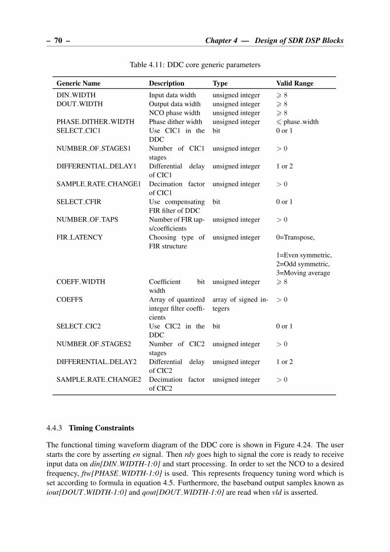
– 70 – Chapter 4 — Design of SDR DSP Blocks
Table 4.11: DDC core generic parameters
Generic Name Description Type Valid Range
DIN WIDTH Input data width unsigned integer > 8
DOUT WIDTH Output data width unsigned integer > 8
NCO phase width unsigned integer > 8
PHASE DITHER WIDTH Phase dither width unsigned integer 6 phase width
SELECT CIC1 Use CIC1 in the
DDC
bit 0 or 1
NUMBER OF STAGES1 Number of CIC1
stages
unsigned integer > 0
DIFFERENTIAL DELAY1 Differential delay
of CIC1
unsigned integer 1 or 2
SAMPLE RATE CHANGE1 Decimation factor
of CIC1
unsigned integer > 0
SELECT CFIR Use compensating
FIR filter of DDC
bit 0 or 1
NUMBER OF TAPS Number of FIR tap-
s/coefficients
unsigned integer > 0
FIR LATENCY Choosing type of
FIR structure
unsigned integer 0=Transpose,
1=Even symmetric,
2=Odd symmetric,
3=Moving average
COEFF WIDTH Coefficient bit
width
unsigned integer > 8
COEFFS Array of quantized
integer filter coeffi-
cients
array of signed in-
tegers
> 0
SELECT CIC2 Use CIC2 in the
DDC
bit 0 or 1
NUMBER OF STAGES2 Number of CIC2
stages
unsigned integer > 0
DIFFERENTIAL DELAY2 Differential delay
of CIC2
unsigned integer 1 or 2
SAMPLE RATE CHANGE2 Decimation factor
of CIC2
unsigned integer > 0
4.4.3 Timing Constraints
The functional timing waveform diagram of the DDC core is shown in Figure 4.24. The user
starts the core by asserting en signal. Then rdy goes high to signal the core is ready to receive
input data on din[DIN WIDTH-1:0] and start processing. In order to set the NCO to a desired
frequency, ftw[PHASE WIDTH-1:0] is used. This represents frequency tuning word which is
set according to formula in equation 4.5. Furthermore, the baseband output samples known as
iout[DOUT WIDTH-1:0] and qout[DOUT WIDTH-1:0] are read when vld is asserted.

Chapter 4 — Design of SDR DSP Blocks – 71 –
Table 4.12: DDC core pin-out
Pin name I/O Description Active State
clk in System Clock Rising edge
rst in System Reset high
en in Clock enable high
din[DIN WIDTH-1:0] in Real valued data sample data
ftw[PHASE WIDTH-1:0] in Frequency Tuning Word data
rdy out DDC core ready to accept input data high
vld out Valid output data available high
clko out Decimated or divided clock Rising edge
iout[DOUT WIDTH-1:0] out Real output sample data
qout[DOUT WIDTH-1:0] out Imaginary output sample data
clk
rst
en
rdy
din [W-1:0]
vld
iout [W-1:0]
iout [W-1:0]
data
Δt=Rcic1×Rcic2×Tclk
Tclk=10ns
Δt = Nin × Tclk
data
data data
data data
data
ftw [W-1:0]
data
Figure 4.24: DDC core input/output timing waveform
4.4.4 Wishbone Interface
The DDC core is made to support SoC design integration by connecting to it a DDC Wishbone
slave interface core as illustrated in Figure 4.25. The slave interface is composed of both wish-
bone ports and high speed parallel ports. The common control ports namely clk,rst and en are to
similar ports used by DDC core as described in Table 4.11 while the Wishbone interface ports
are described in section 2.12.
The signals in Figure 4.25 are classified into feedforward and feedback signals. The feedforward
signals transfer data from DDC slave block to a DDC core. These include a start/en signal
which activates DDC core processing while a signal connecting ftw[15:0] ports on both blocks
is used to input the frequency tuning word to the DDC core. The dout[15:0] port presents input

– 72 – Chapter 4 — Design of SDR DSP Blocks
clkrsten
start
DDC Slave Interface
ftw [31..0]
wbs_stb_iwbs_cyc_i
wbs_adr_i [15..0]
wbs_dat_i [15..0]
dinr [15..0]
wbs_ack_o
wbs_dat_o [31..0]
dini [15..0]dout [15..0]
clkrsten
din [15..0]
vld
DDC core
iout [15..0]ftw [31..0]
qout [15..0]
Figure 4.25: DDC core and Wishbone slave interface
samples to the DDC core via direct connection with din[15:0] port on the DDC core.
Additionally, the feedback signals transfer DDC core output data to the input interface of a
slave block. These include the vld/en signal which indicates the valid data output from DDC
core. The data samples processed by a DDC core are sent to a slave core via iout[15:0] and
qout[15:0] I/Q ports which in turn connect to a dinr[15:0] and dini[15:0] ports of a slave
interface respectively.
Furthermore, the description of DDC Wishbone slave interface registers is provided in Ta-
ble 4.13. The slave select is a read-only register that provides a unique identifier in the SoC
design. The DDC core is activated by setting the write-only control register while the read-only
status signals the end of DDC process. The frequency tuning word is held by a write-only
FTW register. The 16-bit write-only input sample register is used for input sample of the DDC
core. Lastly the ouput sample is a read-only output register whose bits are 32-bits which is a
combination of 16-bit real output sample and 16-bit imaginary output sample.

Chapter 4 — Design of SDR DSP Blocks – 73 –
Table 4.13: Wishbone slave registers for DDC core
Register Address Register Value Bits
slave select 0x0000 16
status 0x0001 1
control 0x0002 1
FTW 0x0003 32
input sample 0x0004 15
output sample 0x0005 32
4.4.5 DDC Core Test
The DDC core test is presented later in section 7.4 using only parallel interface and not Wish-
bone bus interface.

CHAPTER 5
DESIGN OF SDR I/O INTERFACE
BLOCKS
This chapter presents design and development of input/output (I/O) interface cores for RHINO.
The design of ADC/DAC interface of FMC150 is discussed first and this is followed by a design
of interface for 1 Gigabit Ethernet using UDP protocol to transmit and receive data packets.
5.1 4DSP-FMC150 INTERFACE CORE
FPGA devices perform all the tasks in the digital domain. As a result, they are used in high-
performance and high-speed applications because digital systems exhibit close-to-ideal char-
acteristics of signal processing. However, the external environment of FPGAs is composed of
complex analog signals with the exception of other digital devices that are physically linked with
the FPGA. Due to the real world that operates in an analog domain, the signal transmission and
reception is performed in an analog domain using DAC and ADC daughter cards respectively.
In this project, a 4DSP-FMC150 FMC daughter card is used as a high performance ADC /DAC
card to perform necessary signal conversions. The card plugs into the LPC FMC standard
connector of RHINO where the FMC connector is linked to RHINO Spartan 6 FPGA via LVDS
interface.
The FMC150 is designed with TIs ADS62P49/ADS4249 dual-channel 14-bit 250Msps ADC
and TIs DAC3283 dual channel 16-bit 800Msps DAC. The TIs CDCE72010 PLL is the clock
distribution device that provides a clock to drive the DAC and ADC. The internal clock source
can optionally be locked to onboard 100 MHz or external reference clock [1].
In order to operate, control and monitor FMC150 card and make it compatible with RHINO, an
FPGA- based interface should be implemented. Although the card is shipped with the reference
design for several commercially available FPGA boards to allow consumers to start using it
quickly, RHINO does not support the FMC150 yet.
This section presents a design of the 4DSP-FMC150 physical interface to the ADC and DAC
with the aid of FMC150 control block via SPI that forms part of the 4DSP consumer reference
design. The sampling rates can be changed according to user application requirements via SPI
74
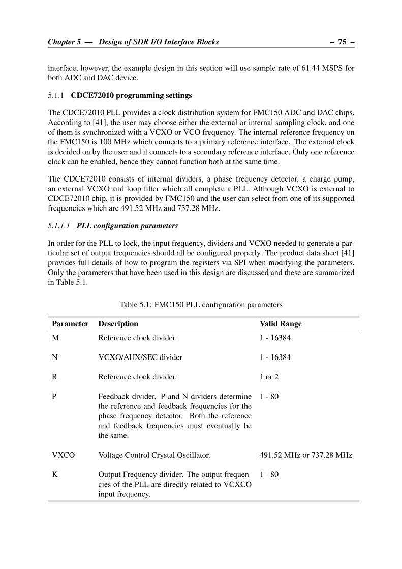
Chapter 5 — Design of SDR I/O Interface Blocks – 75 –
interface, however, the example design in this section will use sample rate of 61.44 MSPS for
both ADC and DAC device.
5.1.1 CDCE72010 programming settings
The CDCE72010 PLL provides a clock distribution system for FMC150 ADC and DAC chips.
According to [41], the user may choose either the external or internal sampling clock, and one
of them is synchronized with a VCXO or VCO frequency. The internal reference frequency on
the FMC150 is 100 MHz which connects to a primary reference interface. The external clock
is decided on by the user and it connects to a secondary reference interface. Only one reference
clock can be enabled, hence they cannot function both at the same time.
The CDCE72010 consists of internal dividers, a phase frequency detector, a charge pump,
an external VCXO and loop filter which all complete a PLL. Although VCXO is external to
CDCE72010 chip, it is provided by FMC150 and the user can select from one of its supported
frequencies which are 491.52 MHz and 737.28 MHz.
5.1.1.1 PLL configuration parameters
In order for the PLL to lock, the input frequency, dividers and VCXO needed to generate a par-
ticular set of output frequencies should all be configured properly. The product data sheet [41]
provides full details of how to program the registers via SPI when modifying the parameters.
Only the parameters that have been used in this design are discussed and these are summarized
in Table 5.1.
Table 5.1: FMC150 PLL configuration parameters
Parameter Description Valid Range
M Reference clock divider. 1 - 16384
N VCXO/AUX/SEC divider 1 - 16384
R Reference clock divider. 1 or 2
P Feedback divider. P and N dividers determine
the reference and feedback frequencies for the
phase frequency detector. Both the reference
and feedback frequencies must eventually be
the same.
1 - 80
VXCO Voltage Control Crystal Oscillator. 491.52 MHz or 737.28 MHz
K Output Frequency divider. The output frequen-
cies of the PLL are directly related to VCXCO
input frequency.
1 - 80

– 76 – Chapter 5 — Design of SDR I/O Interface Blocks
5.1.1.2 PLL Design
Our design application requires three different clocks which are described as below:
1. 61.44 MHz output clock 2 (Fout2) - This is configured as LVPECL output and provides
a sampling clock for ADC (ads62p49 chip).
2. 245.76 MHz output clock 4 (Fout4) - The clock is configured as LVDS and connects to
the FMC connector to supply reference clock for the DAC clock and data signals inside
the FPGA. CLK TO FPGA P/N is used on the FPGA side to connect to the input clock
reference.
3. 245.76 MHz output clock 7 (Fout7) - This is configured as LVPECL output and provides
a clock for DAC (dac3283 chip).
The output frequencies are phase-locked to onboard 100 MHz input reference clock that is
connected to a PRI REF pin of cdce72010. The VCXO frequency is chosen as 491.52 MHz
and this is also provided by FMC150 board. With the above parameters chosen, the goal is to
now determine M , N , feedback (P ), and output divider values (K). The relationship between
the VCXO frequency and the input reference voltage is related by equation 5.1.
FVCXO IN or FAUX IN
Frequency (PRI REF or SEC REF)=
P ×M
R×N
Where :
FVCXO = Fout ×K
Provided that :
Fout ×K < 1500MHz
(5.1)
Since the internal reference frequency is used, we choose M = 625, R = 1 and PFD = 160
kHz as recommended by the vendor [1]. At this point, the remaining unknowns are feedback
dividers N and P . Choosing P = 8, the relationship in equation 5.1 is now used to determine
N as shown in equation 5.2.
N =FVCXO IN ×R×M
FPRI REF × P
=491.52× 106 × 1× 625
100× 106 × 8
= 384
(5.2)
The output dividers are calculated as follows:
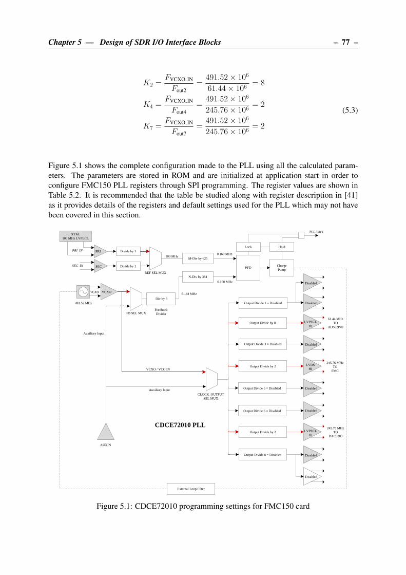
Chapter 5 — Design of SDR I/O Interface Blocks – 77 –
K2 =FVCXO IN
Fout2
=491.52× 10⁶
61.44× 106= 8
K4 =FVCXO IN
Fout4
=491.52× 10⁶
245.76× 106= 2
K7 =FVCXO IN
Fout7
=491.52× 10⁶
245.76× 106= 2
(5.3)
Figure 5.1 shows the complete configuration made to the PLL using all the calculated param-
eters. The parameters are stored in ROM and are initialized at application start in order to
configure FMC150 PLL registers through SPI programming. The register values are shown in
Table 5.2. It is recommended that the table be studied along with register description in [41]
as it provides details of the registers and default settings used for the PLL which may not have
been covered in this section.
REF SEL MUX
Divide by 1
Divide by 1
M-Div by 625
N-Div by 384
PFD
Lock
ChargePump
Hold
Output Divide 1 = Disabled
Output Divide by 8
Output Divide 3 = Disabled
Output Divide by 2
Output Divide 5 = Disabled
Output Divide 6 = Disabled
Output Divide by 2
Output Divide 8 = Disabled
FB SEL MUX
Div by 8
External Loop Filter
VCXO VCXO
PRI
SEC
XTAL100 MHz LVPECL
SEC_IN
PRI_IN
Auxiliary Input
VCXO / VCO IN
Auxiliary Input
AUXIN
Feedback Divider
491.52 MHz
PLL Lock
LVPECLHI
LVDSHI
LVPECLHI
Disabled
Disabled
Disabled
Disabled
Disabled
Disabled
Disabled
CDCE72010 PLL
61.44 MHzTO
ADS62P49
245.76 MHzTO
FMC
245.76 MHzTO
DAC3283
0.160 MHz
0.160 MHz
100 MHz
61.44 MHz
CLOCK_OUTPUT SEL MUX
Figure 5.1: CDCE72010 programming settings for FMC150 card
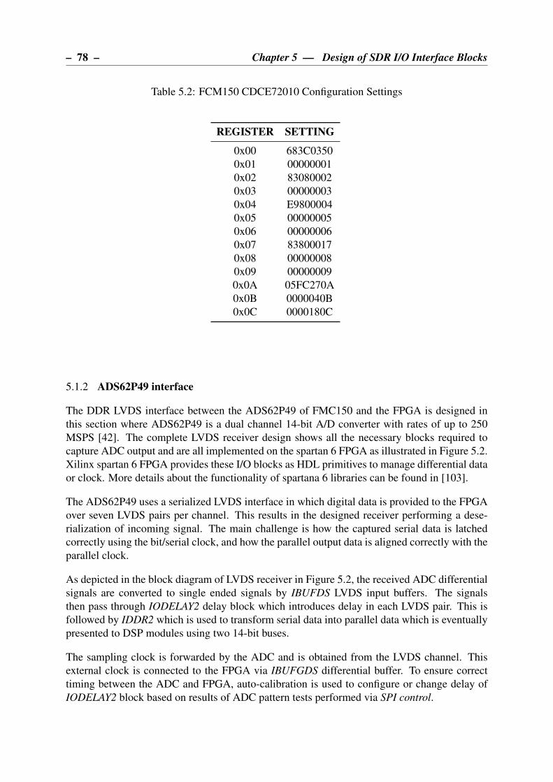
– 78 – Chapter 5 — Design of SDR I/O Interface Blocks
Table 5.2: FCM150 CDCE72010 Configuration Settings
REGISTER SETTING
0x00 683C0350
0x01 00000001
0x02 83080002
0x03 00000003
0x04 E9800004
0x05 00000005
0x06 00000006
0x07 83800017
0x08 00000008
0x09 00000009
0x0A 05FC270A
0x0B 0000040B
0x0C 0000180C
5.1.2 ADS62P49 interface
The DDR LVDS interface between the ADS62P49 of FMC150 and the FPGA is designed in
this section where ADS62P49 is a dual channel 14-bit A/D converter with rates of up to 250
MSPS [42]. The complete LVDS receiver design shows all the necessary blocks required to
capture ADC output and are all implemented on the spartan 6 FPGA as illustrated in Figure 5.2.
Xilinx spartan 6 FPGA provides these I/O blocks as HDL primitives to manage differential data
or clock. More details about the functionality of spartana 6 libraries can be found in [103].
The ADS62P49 uses a serialized LVDS interface in which digital data is provided to the FPGA
over seven LVDS pairs per channel. This results in the designed receiver performing a dese-
rialization of incoming signal. The main challenge is how the captured serial data is latched
correctly using the bit/serial clock, and how the parallel output data is aligned correctly with the
parallel clock.
As depicted in the block diagram of LVDS receiver in Figure 5.2, the received ADC differential
signals are converted to single ended signals by IBUFDS LVDS input buffers. The signals
then pass through IODELAY2 delay block which introduces delay in each LVDS pair. This is
followed by IDDR2 which is used to transform serial data into parallel data which is eventually
presented to DSP modules using two 14-bit buses.
The sampling clock is forwarded by the ADC and is obtained from the LVDS channel. This
external clock is connected to the FPGA via IBUFGDS differential buffer. To ensure correct
timing between the ADC and FPGA, auto-calibration is used to configure or change delay of
IODELAY2 block based on results of ADC pattern tests performed via SPI control.
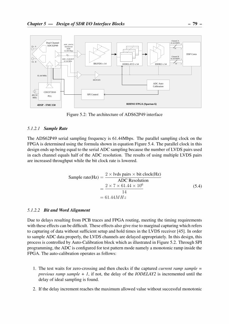
Chapter 5 — Design of SDR I/O Interface Blocks – 79 –
ADC Auto Calibration
DSP Cores
SPI ControlCDCE72010
PLL
IDDR2 x 14IODELAY2 x 14IBUFDS x 14
Dual Channel ADC62P49 ADC_DATA
InterleavedDDR
122.88 Mbps
ADC_CLKOUT61.44 MHz
14
IBUFGDS
Channel A61.44 MSPS
Channel B61.44 MSPS
4DSP - FMC150 RHINO FPGA (Spartan 6)
491.52 MHz
61.44 MHz
Ch - A
Ch - B14
14
Figure 5.2: The architecture of ADS62P49 interface
5.1.2.1 Sample Rate
The ADS62P49 serial sampling frequency is 61.44Mbps. The parallel sampling clock on the
FPGA is determined using the formula shown in equation Figure 5.4. The parallel clock in this
design ends up being equal to the serial ADC sampling because the number of LVDS pairs used
in each channel equals half of the ADC resolution. The results of using multiple LVDS pairs
are increased throughput while the bit clock rate is lowered.
Sample rate(Hz) =2× lvds pairs × bit clock(Hz)
ADC Resolution
=2× 7× 61.44× 106
14= 61.44MHz
(5.4)
5.1.2.2 Bit and Word Alignment
Due to delays resulting from PCB traces and FPGA routing, meeting the timing requirements
with these effects can be difficult. These effects also give rise to marginal capturing which refers
to capturing of data without sufficient setup and hold times in the LVDS receiver [45]. In order
to sample ADC data properly, the LVDS channels are delayed appropriately. In this design, this
process is controlled by Auto-Calibration block which as illustrated in Figure 5.2. Through SPI
programming, the ADC is configured for test pattern mode namely a monotonic ramp inside the
FPGA. The auto-calibration operates as follows:
1. The test waits for zero-crossing and then checks if the captured current ramp sample =
previous ramp sample + 1, if not, the delay of the IODELAY2 is incremented until the
delay of ideal sampling is found.
2. If the delay increment reaches the maximum allowed value without successful monotonic

– 80 – Chapter 5 — Design of SDR I/O Interface Blocks
ramp, the whole calibration is considered to have failed.
3. For successful test, an error free ramp over set maximum value of ramp must be received.
4. After successful search of an ideal delay, the delay is applied globally to two ADC chan-
nels. The pass of this test provides enough confidence in set timing requirements for
interface between ADC and FPGA.
5.1.3 DAC3283 interface
The DAC3283 is a dual channel 16-bit 800 MSPS digital-to-analog converter with an 8-bit
LVDS input data bus with on-chip termination, optional 2x and 4x interpolation filters, digital
IQ compensation and internal voltage reference. It has a single 8-bit LVDS bus that accepts
dual, 16-bit data input in byte-wide format [43].
This section provides a description for DAC interface design using Spartan6 FPGA. Although
the DAC3283 is capable of operating at sampling rate as high as 800 MSPS, only 61.44 MSPS
DAC rate is realized in this design. The same process of design can be adapted in other lower
or higher sampling rate designs.
The DAC interface module takes data on the parallel side and performs 16:1 serialization over
the single 8-bit LVDS bus. In a basic application with a just 1-bit LVDS bus, the resulting serial
frequency would be 32 times higher than parallel frequency if DDR clock were used and data
of two channels were interleaved over a single 1-bit LVDS channel. However, these figures
reduce drastically as DAC3283 uses 8-bit LVDS bus to serialize and interleave dual channel 16-
bit samples using a DDR sampling clock. Therefore the LVDS interface has two clock inputs,
namely adcclock (serial adc data clock) and divclock(parallel side clock). The equation for
calculating adcclock is shown in equation 5.5.
fadcclock =fdivclock × sample width × 2 (Dual Channel Interleaved)
lvds pairs × 2 (DDR used)
=61.44 MSPS × 16× 2
8× 2
= 122.88 MSPS
(5.5)
where fadcclock is serial adc data clock frequency and fdivclock is parallel side clock frequency.
The resulting data clock sampling rate of a DAC is 122.88 MSPS when the parallel clock of
61.44 MHz is used. The calculation is shown in equation 5.5 and the schematic of DAC LVDS
interface is illustrated in Figure 5.3. Serialization is done by OSERDES2 components which
are available in input/out blocks library of Xilinx Spartaran6 [103]. The MMCM (Mixed Mode
Clock Management) block receives a 245.76 MHz clock routed from the FMC150 to an FPGA.
It generates multiple clocks derived from the input clock. The clocks are distributed to DSP
cores, the OSERSES2 and a DAC.
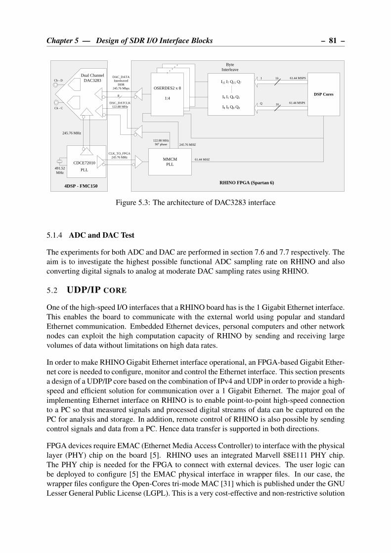
Chapter 5 — Design of SDR I/O Interface Blocks – 81 –
I15 I7 Q15 Q7
I9 I1 Q9 Q1
I8 I0 Q8 Q0
DSP Cores
MMCMPLLCDCE72010
PLL
OSERDES2 x 8
1:4
Dual Channel DAC3283
DAC_DATAInterleaved
DDR245.76 Mbps
DAC_DATCLK122.88 MHz
8
61.44 MSPS
61.44 MSPS
4DSP - FMC150RHINO FPGA (Spartan 6)
491.52 MHz
245.76 MHz
Ch - D
Ch - C
Byte Interleave
Q
122.88 MHz90o phase 245.76 MHZ
I
61.44 MHZ
16
16
CLK_TO_FPGA245.76 MHz
Figure 5.3: The architecture of DAC3283 interface
5.1.4 ADC and DAC Test
The experiments for both ADC and DAC are performed in section 7.6 and 7.7 respectively. The
aim is to investigate the highest possible functional ADC sampling rate on RHINO and also
converting digital signals to analog at moderate DAC sampling rates using RHINO.
5.2 UDP/IP CORE
One of the high-speed I/O interfaces that a RHINO board has is the 1 Gigabit Ethernet interface.
This enables the board to communicate with the external world using popular and standard
Ethernet communication. Embedded Ethernet devices, personal computers and other network
nodes can exploit the high computation capacity of RHINO by sending and receiving large
volumes of data without limitations on high data rates.
In order to make RHINO Gigabit Ethernet interface operational, an FPGA-based Gigabit Ether-
net core is needed to configure, monitor and control the Ethernet interface. This section presents
a design of a UDP/IP core based on the combination of IPv4 and UDP in order to provide a high-
speed and efficient solution for communication over a 1 Gigabit Ethernet. The major goal of
implementing Ethernet interface on RHINO is to enable point-to-point high-speed connection
to a PC so that measured signals and processed digital streams of data can be captured on the
PC for analysis and storage. In addition, remote control of RHINO is also possible by sending
control signals and data from a PC. Hence data transfer is supported in both directions.
FPGA devices require EMAC (Ethernet Media Access Controller) to interface with the physical
layer (PHY) chip on the board [5]. RHINO uses an integrated Marvell 88E111 PHY chip.
The PHY chip is needed for the FPGA to connect with external devices. The user logic can
be deployed to configure [5] the EMAC physical interface in wrapper files. In our case, the
wrapper files configure the Open-Cores tri-mode MAC [31] which is published under the GNU
Lesser General Public License (LGPL). This is a very cost-effective and non-restrictive solution
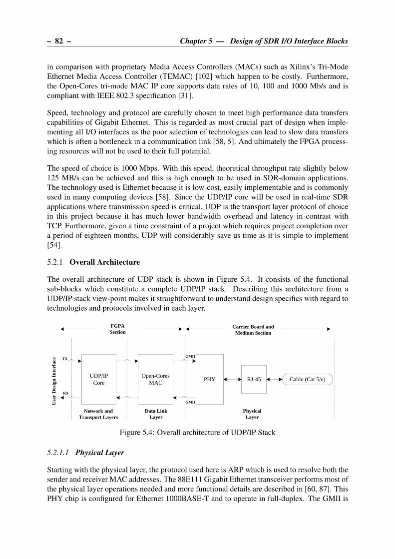
– 82 – Chapter 5 — Design of SDR I/O Interface Blocks
in comparison with proprietary Media Access Controllers (MACs) such as Xilinx’s Tri-Mode
Ethernet Media Access Controller (TEMAC) [102] which happen to be costly. Furthermore,
the Open-Cores tri-mode MAC IP core supports data rates of 10, 100 and 1000 Mb/s and is
compliant with IEEE 802.3 specification [31].
Speed, technology and protocol are carefully chosen to meet high performance data transfers
capabilities of Gigabit Ethernet. This is regarded as most crucial part of design when imple-
menting all I/O interfaces as the poor selection of technologies can lead to slow data transfers
which is often a bottleneck in a communication link [58, 5]. And ultimately the FPGA process-
ing resources will not be used to their full potential.
The speed of choice is 1000 Mbps. With this speed, theoretical throughput rate slightly below
125 MB/s can be achieved and this is high enough to be used in SDR-domain applications.
The technology used is Ethernet because it is low-cost, easily implementable and is commonly
used in many computing devices [58]. Since the UDP/IP core will be used in real-time SDR
applications where transmission speed is critical, UDP is the transport layer protocol of choice
in this project because it has much lower bandwidth overhead and latency in contrast with
TCP. Furthermore, given a time constraint of a project which requires project completion over
a period of eighteen months, UDP will considerably save us time as it is simple to implement
[54].
5.2.1 Overall Architecture
The overall architecture of UDP stack is shown in Figure 5.4. It consists of the functional
sub-blocks which constitute a complete UDP/IP stack. Describing this architecture from a
UDP/IP stack view-point makes it straightforward to understand design specifics with regard to
technologies and protocols involved in each layer.
Open-Cores MAC
PHYUDP/IP
CoreRJ-45 Cable (Cat 5/e)
Network and Transport Layers
Data LinkLayer
PhysicalLayer
Use
r D
esig
n In
terf
ace
GMII
GMII
FGPA Section
Carrier Board and Medium Section
TX
RX
Figure 5.4: Overall architecture of UDP/IP Stack
5.2.1.1 Physical Layer
Starting with the physical layer, the protocol used here is ARP which is used to resolve both the
sender and receiver MAC addresses. The 88E111 Gigabit Ethernet transceiver performs most of
the physical layer operations needed and more functional details are described in [60, 87]. This
PHY chip is configured for Ethernet 1000BASE-T and to operate in full-duplex. The GMII is

Chapter 5 — Design of SDR I/O Interface Blocks – 83 –
used as a standard data interface between a MAC and PHY chip while the MDIO bus is used
to send the configuration data from the MAC to a PHY. The PHY then connects to a CAT-5/e
cable through RJ-45 connector.
5.2.1.2 Data Link Layer
The data link layer comprises an Open-Cores tri-mode MAC which is responsible for delivering
data over a shared physical channel. The MAC consists of three user interfaces that simplify
the connection to a MAC core. The MAC is responsible for encoding and decoding user data
to/from GMII and MDIO signals. One interface is used for data transmission, another one for
data reception and the last one for configuration of PHY chip. All signals of the interface are
clocked at the rising edge of Clk user.
The transmit interface of the of the MAC is shown in Figure 5.5. This is used to send custom
packets of different protocols to a destination device. In our case, UDP and ARP protocol
packets are sent and will be discussed in more detail in later sections.
Clk_user
Tx_mac_wa
Tx_mac_wr
Tx_mac_sop
Tx_mac_eop
Tx_mac_data [31:0]
Tx_mac_BE [2:0]
data data
data
Figure 5.5: MAC core transmit operation [31]
Tx mac wa remains high to indicate available space in the transmit FIFO of a MAC. When
Tx mac wr is high, it denotes that data write is ready and therefore Tx mac sop which signals
a start of packet operation is quickly set high for one clock cycle. The packet data is then sent
into MAC FIFO via 32-bit Tx mac data[31:0] bus. Data write to FIFO is paused each time
Tx mac wr goes low and resumes when Tx mac wr goes high. Tx mac eop signals the end of
the packet and is set high for one clock cycle. The Tx mac BE[2:0] is used for byte enable. The
number of bytes and the corresponding values of Tx mac BE[2:0] are described in Table 5.3.
Since our application use 32-bit bus to transmit packets, “00” is used as the value of a byte
enable signal.
Table 5.3: Byte Enable Configurations
Tx mac BE[2:0] and Rx mac BE[2:0] (binary) Number of bytes
00 4
01 1
10 2
11 3
Furthermore, the receiver interface of the MAC is illustrated in Figure 5.6. This is used to re-
ceive packets from the sender, that is, UDP and ARP packets from a remote device are received

– 84 – Chapter 5 — Design of SDR I/O Interface Blocks
by the user logic. Rx mac ra is a read-available signal that denotes the availability of data in
the receive FIFO of the MAC. It also signals the package has been received successfully and
is ready to be saved or read. Rx mac rd is asserted as long as the Rx mac ra signal is high to
enable output of data received. The Rx mac pa also known as “package-available” signals the
valid read data on 32-bit Rx mac data[31:0] bus. Both the Rx mac sop and Rx mac eop are
used to signal start of packet and end of packet respectively. The Rx mac BE[2:0] works in the
same manner as Tx mac BE[2:0] above to hold the byte enable value.
Clk_user
Rx_mac_ra
Rx_mac_rd
Rx_mac_pa
Rx_mac_sop
Rx_mac_eop
Rx_mac_data [31:0]
Rx_mac_BE [2:0]
data data
data
Figure 5.6: MAC core receive operation [31]
MDIO is used for configuration and status read of the PHY device. The MAC provides a sim-
plified interface to MDIO as described in [62]. Using the FPGA user logic, the write operation
is initiated by asserting WctrlData as shown in Figure 5.7. At this point, the PHY device ad-
dress Fiad[4:0], the configuration data Ctld[15:0], the PHY register address Rgad[4:0] must
hold valid values. The Busy signal goes high as soon as the write operation begins and it signals
operation completion when it goes low.
The status read process starts by asserting Rstat. It also indicates that the Fiad[4:0] and
Rgad[4:0] are valid. The Busy signal goes high to indicate that read operation is in progress.
When the Busy signal goes low, it signals the valid status data on Prsd[15:0] line. Finally, the
NoPre indicates that the preamble is sent when its set low. When it is high it means there is no
preamble in the sent configuration data.
Clk_user
WctrlData
Rstat
Fiad [4:0]
Rgad [4:0]
Prsd [15:0]
Ctld [15:0]
Busy
Nopre
data
data
data data
data
data
Figure 5.7: PHY Management interface
The MAC core also has specific configurations to control the core operation itself. Unlike the
PHY Configuration which is done via MDIO interface, the MAC core configurations are per-
formed by simply changing the constant register values in a configuration ROM. The registers

Chapter 5 — Design of SDR I/O Interface Blocks – 85 –
are fully described in [31]. Table 5.4 only shows the configurations that have been modified for
RHINO UDP core while the rest remain default.
Table 5.4: MAC core register description
Register Name Address (hex) Value (hex) Description
tx pause en 011 0001 Enables MAC to pause
transmission when
transmit FIFO is full.
CRC chk en 024 0001 Enables dropping of
packets with FCS
checksum error.
Speed 034 0004 Sets the Ethernet MAC
core’s speed level to
1000 Mbps
5.2.1.3 Network Layer
ARP is a network layer protocol used at data-link layer to map IP address to MAC address for
hop-to-hop communication. Furthermore, in network layer, the internet protocol (IPv4) is used
by the designed UDP core to deliver messages between the RHINO and destination device. The
IP addresses are configured statically and they must be in the same subnetwork for successful
communication to happen.
5.2.1.4 Transport Layer
Lastly UDP is chosen as a transport layer protocol. It is used in this design for its simplicity
and the fact that it supports high speed and real-time data transfers.
5.2.2 Structure of the UDP/IP core
The architecture of the UDP core is illustrated in Figure 5.8. It consists of a UDP wrapper
which simplifies usage of the core. It also has a MAC wrapper provided by open-cores which
substantially reduces development time by providing functions needed to connect to PHY. The
FIFOs of the MAC are driven by a system reference clock of 100 MHz. The UDP core provides
GMII interface to a PHY and another interface to user design logic. On the GMII interface, the
globally routed 125 MHz clock is needed to operate GMII transmit operation. While the PHY
provides 125 MHz reference clock, this is not used. Rather, a 125 MHz clock is derived from
the system clock using PLL primitive of spartan 6. Using ODDR2 on the spartan 6, the clock
is driven and fed to the external GIGE GTX CLK output pin. If the ODDR2 is not used, the
clock will never work. GMII receive operation is also driven by a 125 reference clock namely
GIGE RX CLK which is generated by PHY.
The UDP wrapper core consists of sub-blocks which make it possible to send and receive ARP
and UDP packets. The cores simplify the user design logic by storing static header fields of the

– 86 – Chapter 5 — Design of SDR I/O Interface Blocks
UDP_TX
ARP
TX_bridge
UDP_RX RX_bridge
Open CoresTri-mode Ethernet MAC
GIGE_COL
GIGE_CRS
GIGE_MDC
GIGE_MDIO
GIGE_TX_CLK
GIGE_nRESET
GIGE_RXD
GIGE_RX_CLK
GIGE_RX_DV
GIGE_RX_ER
GIGE_TXD
GIGE_GTX_CLK
GIGE_TX_EN
GIGE_TX_ER
udp_tx_pkt_data
udp_rx_pkt_data
own_ip_addr own_mac_addr dst_ip_addr dst_mac_addr
udp_tx_pkt_vld
udp_tx_rdy
udp_rx_pkt_req
udp_rx_rdy
sys_clk
sys_rst
UDP_Wrapper
UDP_1GbE core
udp_src_port udp_dst_port mac_init_done
PH
Y (
Mar
vell
8811
1) in
terf
ace
32
32
n
n
16 16
32 48 32 48
Figure 5.8: Structure of UDP/IP Core based on a Gigabit Ethernet
ARP and UDP packets in the lookup table. Only dynamic data such as the ports, ip addresses
and payload are sent to the core by the user.
The ARP block enables the ARP process when the core initializes. This happens seamlessly
and it takes place before the actual UDP packets can be sent or received. It is important that
before communication the RHINO board and the remote device know each other’s IP and MAC
address. Initially, both devices already know each other’s IP addresses as they are statically
configured but they have no knowledge of the MAC addresses. This is where ARP is used to
resolve the MAC addresses when the IP addresses are known by both devices.
The ARP process begins with the FPGA that sends a broadcast ARP request together with its
own MAC and IP addresses and a destination IP address and polls for ARP response from a
remote device. After the ARP response is received, it updates the ARP table with the received
MAC address and soon after this the UDP transmission is ready to be initiated. The FPGA will
also respond to ARP requests from the remote device in the midst of UDP communication.
The ARP request packet structure is shown in Figure 5.10. The operation field indicates whether
the packet is a request or a response. The value of 0x01 denotes a request and 0x02 shows a
response. The source and destination IP addresses are variable, the source MAC address is
variable too and are all provided in user design, and the rest of the fields are static. The FPGA
ARP request uses the static broadcast address “FF:FF:FF:FF:FF:FF” in the destination MAC
address field of the ARP packet. For the ARP response, the destination MAC address field is
filled with the known MAC address of the remote device.
Moreover, the UDP tx module manages the UDP packet transmission over IP. It uses the inter-
face shown in Figure 5.7 to send data to a destination device. The transmission requires that
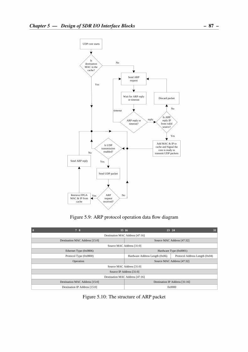
Chapter 5 — Design of SDR I/O Interface Blocks – 87 –
Is destination MAC in the
cache?
UDP core starts
Send ARPrequest
Wait for ARP reply or timeout
ARP reply or timeout?
Is ARP reply IP
from valid source?
Add MAC & IP to cache and Signal the
core is ready to transmit UDP packets
ARP request
received?
Retrieve FPGA MAC & IP from
cache
Send ARP reply
timeout
Yes
Discard packet
reply
No
Yes
NoYes
No
Is UDP transmission
enabled?
Send UDP packet
Yes
No
Figure 5.9: ARP protocol operation data flow diagram
0 7 15 23 318 16
Destination MAC Address [47:16]
24
Destination MAC Address [15:0] Source MAC Address [47:32]
Source MAC Address [31:0]
Ethernet Type (0x0806) Hardware Type (0x0001)
Protocol Type (0x0800) Hardware Address Length (0x06) Protocol Address Length (0x04)
Operation Source MAC Address [47:32]
Source MAC Address [31:0]
Source IP Address [31:0]
Destination MAC Address [47:16]
Destination MAC Address [15:0] Destination IP Address [31:16]
Destination IP Address [15:0] 0x0000
Figure 5.10: The structure of ARP packet

– 88 – Chapter 5 — Design of SDR I/O Interface Blocks
the user provides source and destination IP and MAC addresses along with the UDP source and
destination ports. The user design also provides payload. The maximum number of bytes in the
payload is 1500.
The UDP packet structure is illustrated in Figure 5.11. It comprises the MAC, UDP and IPv4
headers. The transmitter attaches four bytes of checksum to the end of each packet. This is
required to check the integrity of data when it arrives at the destination. The total length field
is calculated as the sum of 20 bytes of IP header, 8 bytes of UDP header and payload length.
While the length field is the sum of 8 bytes of UDP header and payload length.
0 7 15 23 318 16
Destination MAC Address [47:16]
24
Destination MAC Address [15:0] Source MAC Address [47:32]
Source MAC Address [31:0]
Ethernet Type (0x0806) Different Services
Total Length Identification
Flags/Fragment offset Time to live
Header Checksum
Source IP Address [15:0]
Destination IP Address [15:0]
Destination Port Length
Checksum Data
Version Header
Protocol
Source IP Address [31:16]
Destination IP Address [31:16]
Source Port
Data
Figure 5.11: The structure of a UDP packet
Lastly the UDP rx block takes of received UDP packets sent by a remote device. The UDP
packets are read using the receive interface shown in Figure 5.6. The destination IP and MAC
addresses of UDP packets received must match with FPGA configured addresses, else the pack-
ets are dropped. The packets are also dropped if the checksum is incorrect. The maximum
receiver payload still remains as 1500 bytes. The structure of the received UDP packet never
changes and still looks like the one shown in Figure 5.11.
5.2.3 Marvell 88E1111S/PHY initialization
The designed UDP/IP core initialization process configures the PHY register settings accord-
ingly before the actual UDP communication begins. MDIO is a serial communication bus that
is used to transfer data between a MAC and a PHY when configuration and Status Read occurs.
The PHY address used in serial communication is 0x01. Table 5.5 shows a state machine that
is used to initialize the PHY. In each state, the register write occurs and it is followed by a read
operation of the same register address. The write operation is considered successful when the
written and read register values match. The state machine then progresses to the next state when
the write is successful else initialization fails and the whole initialization process starts anew.
5.2.4 UDP/IP Core Interface
The UDP core is designed to simplify interfacing to the user top-most design entities. With all
the encapsulation and decapsulation of headers in both the ARP and UDP packets taking place
in the UDP core. The user only assigns communications parameters and quickly starts sending
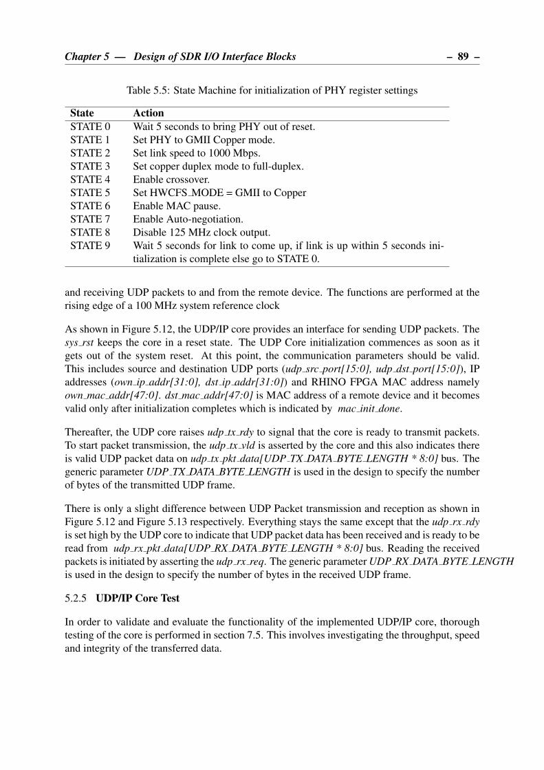
Chapter 5 — Design of SDR I/O Interface Blocks – 89 –
Table 5.5: State Machine for initialization of PHY register settings
State Action
STATE 0 Wait 5 seconds to bring PHY out of reset.
STATE 1 Set PHY to GMII Copper mode.
STATE 2 Set link speed to 1000 Mbps.
STATE 3 Set copper duplex mode to full-duplex.
STATE 4 Enable crossover.
STATE 5 Set HWCFS MODE = GMII to Copper
STATE 6 Enable MAC pause.
STATE 7 Enable Auto-negotiation.
STATE 8 Disable 125 MHz clock output.
STATE 9 Wait 5 seconds for link to come up, if link is up within 5 seconds ini-
tialization is complete else go to STATE 0.
and receiving UDP packets to and from the remote device. The functions are performed at the
rising edge of a 100 MHz system reference clock
As shown in Figure 5.12, the UDP/IP core provides an interface for sending UDP packets. The
sys rst keeps the core in a reset state. The UDP Core initialization commences as soon as it
gets out of the system reset. At this point, the communication parameters should be valid.
This includes source and destination UDP ports (udp src port[15:0], udp dst port[15:0]), IP
addresses (own ip addr[31:0], dst ip addr[31:0]) and RHINO FPGA MAC address namely
own mac addr[47:0]. dst mac addr[47:0] is MAC address of a remote device and it becomes
valid only after initialization completes which is indicated by mac init done.
Thereafter, the UDP core raises udp tx rdy to signal that the core is ready to transmit packets.
To start packet transmission, the udp tx vld is asserted by the core and this also indicates there
is valid UDP packet data on udp tx pkt data[UDP TX DATA BYTE LENGTH * 8:0] bus. The
generic parameter UDP TX DATA BYTE LENGTH is used in the design to specify the number
of bytes of the transmitted UDP frame.
There is only a slight difference between UDP Packet transmission and reception as shown in
Figure 5.12 and Figure 5.13 respectively. Everything stays the same except that the udp rx rdy
is set high by the UDP core to indicate that UDP packet data has been received and is ready to be
read from udp rx pkt data[UDP RX DATA BYTE LENGTH * 8:0] bus. Reading the received
packets is initiated by asserting the udp rx req. The generic parameter UDP RX DATA BYTE LENGTH
is used in the design to specify the number of bytes in the received UDP frame.
5.2.5 UDP/IP Core Test
In order to validate and evaluate the functionality of the implemented UDP/IP core, thorough
testing of the core is performed in section 7.5. This involves investigating the throughput, speed
and integrity of the transferred data.

– 90 – Chapter 5 — Design of SDR I/O Interface Blocks
clkudp_src_port [15:0]
own_mac_addr [47:0]
udp_tx_rdy
udp_tx_vld
udp_tx_pkt_data [W-1:0]
Tclk=10ns
data
mac_init_done
udp_src_port [15:0]
own_ip_addr [31:0]
dst_ip_addr [31:0]
dst_mac_addr [47:0]
rst
data
data
data
data
data
Figure 5.12: UDP Core Write operation interface
clkudp_src_port [15:0]
own_mac_addr [47:0]
udp_rx_req
udp_rx_pkt_data [W-1:0]
mac_init_done
Tclk=10ns
data
udp_rx_rdy
udp_src_port [15:0]
own_ip_addr [31:0]
dst_ip_addr [31:0]
dst_mac_addr [47:0]
rst
data
data
data
data data
Figure 5.13: UDP Core Read operation interface
CHAPTER 6
DESIGN OF FM RECEIVER
This chapter presents the design of a wide-band digital FM receiver to show case rapid applica-
tion development of SDR using a proposed library of reusable IP blocks. Using these IP blocks
which incorporate DSP cores and I/O communication cores, the prototype serves as a proof
of concept that the blocks can be used not only in this FM receiver design, but also in other
real-time SDR applications. Choosing FM receiver is based on the fact that the receiver is more
difficult than a transmitter in terms of software processing. FM is also more complex than other
modulation techniques such AM and it essentially needs more processing blocks. Furthermore,
the licensing issues of spectrum regulation have restrained us to use a freely available FM chan-
nels for receiving and demodulation. The fundamental concepts of frequency modulation and
demodulation are described in section 2.11. The complete design of FM receiver comprises
an RF analogue frontend circuitry and digital receiver which forms the largest part of the FM
receiver processing.
6.1 DESIGN OF DIGITAL RECEIVER
The digital receiver processing is implemented with a DDC core and FM demodulator. The
block diagram showing processing blocks is shown in Figure 6.1. Details of a DDC core oper-
ation have been described in Section 4.4 of Chapter 4.
The 20 MHz bandwidth RF signal is digitized with 14-bit precision ADC of FMC150 card. The
IF signal ranges between 88 MHz and 108 MHz resulting in 20 MHz bandwidth of FM signal.
The digitized FM signal is defined by equation 6.1. Typically, a very high speed ADC of at least
108MHz × 2 = 216MHz is required to digitize the signal. However, this is slightly above
163.84 MHz which is the maximum ADC speed achieved on RHINO.
xFM = Accos[ωcn+ ϕFM [n]],
where,(6.1)
where carrier phase deviation is ϕFM [n] = kvco∑n−1
i=0 SN [i], SN is baseband signal, k(vco) is
frequency sensitivity and xFM is FM signal.
As an alternative to using a high speed ADC, band-pass sampling [97] is employed in this
91
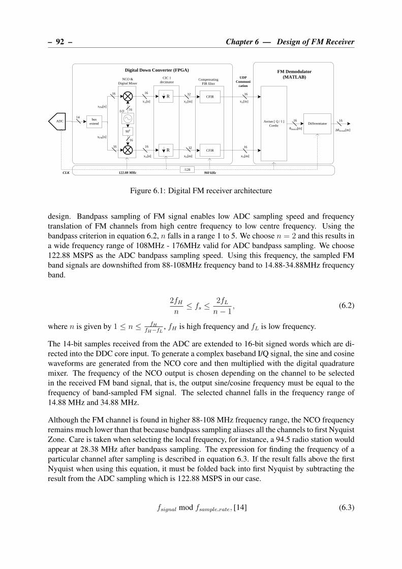
– 92 – Chapter 6 — Design of FM Receiver
900
14
NCO & Digital Mixer
Compensating FIR filter
CIC 1 decimator
Digital Down Converter (FPGA)
Arctan [ Q / I ]Cordic
Differentiator
LO
FM Demodulator (MATLAB)
CFIRR
R CFIR
ADC
122.88 MHz 960 kHz
busextend
16
16 16
16
32
32
16
16
16 16
16
16
/128CLK
xFM[n]
x1r[n]
x1i[n] x2i[m]
x2r[m] x3r[m]
x3i[m]
xFM[n]
θdemod[m] Δθdemod[m]
UDPCommuni
cation
Figure 6.1: Digital FM receiver architecture
design. Bandpass sampling of FM signal enables low ADC sampling speed and frequency
translation of FM channels from high centre frequency to low centre frequency. Using the
bandpass criterion in equation 6.2, n falls in a range 1 to 5. We choose n = 2 and this results in
a wide frequency range of 108MHz - 176MHz valid for ADC bandpass sampling. We choose
122.88 MSPS as the ADC bandpass sampling speed. Using this frequency, the sampled FM
band signals are downshifted from 88-108MHz frequency band to 14.88-34.88MHz frequency
band.
2fHn
≤ fs ≤2fLn− 1
, (6.2)
where n is given by 1 ≤ n ≤ fHfH−fL
, fH is high frequency and fL is low frequency.
The 14-bit samples received from the ADC are extended to 16-bit signed words which are di-
rected into the DDC core input. To generate a complex baseband I/Q signal, the sine and cosine
waveforms are generated from the NCO core and then multiplied with the digital quadrature
mixer. The frequency of the NCO output is chosen depending on the channel to be selected
in the received FM band signal, that is, the output sine/cosine frequency must be equal to the
frequency of band-sampled FM signal. The selected channel falls in the frequency range of
14.88 MHz and 34.88 MHz.
Although the FM channel is found in higher 88-108 MHz frequency range, the NCO frequency
remains much lower than that because bandpass sampling aliases all the channels to first Nyquist
Zone. Care is taken when selecting the local frequency, for instance, a 94.5 radio station would
appear at 28.38 MHz after bandpass sampling. The expression for finding the frequency of a
particular channel after sampling is described in equation 6.3. If the result falls above the first
Nyquist when using this equation, it must be folded back into first Nyquist by subtracting the
result from the ADC sampling which is 122.88 MSPS in our case.
fsignal mod fsample rate, [14] (6.3)
Chapter 6 — Design of FM Receiver – 93 –
For commercial FM broadcasting in South Africa, the maximum frequency deviation ∆f is 75
kHz [46] and Carson’s rule estimates the bandwidth when maximum audio message (fm) of
15kHz is used. The bandwidth is BW ≈ 2(β +1)fm = 2(5+ 1)15kHz = 180kHz where β is
modulation index defined by β = ∆f/fm = 75kHz/15kHz = 5. The commercially allocated
bandwidth for each channel is 200kHz [46]. This information is therefore enough to determine
the cut-off frequency. The cut-off frequency of the filter needs to be slightly above or equal to
BW/2 = 90. This is safest point as the 180 kHz of bandwidth is normally more than enough
relative to information FM broadcasters send in the allocated channel. The selectivity of the
receiver is determined by the designed filter which is 80kHz at -6dB and 150kHz at -60dB. This
is selective enough to isolate the selected channel from closest channels.
After mixing down the FM signal using the quadrature mixer, the image and mixer products
are eliminated by the CIC filter which uses zero multipliers in its implementation. The CIC
filter specification parameters are shown in Table 6.1. This CIC filter also decimates the 122.88
MSPS ADC rate to 960 kSPS by decimating ratio of 1:128. Despite its low cost, efficient and
simple implementation, the CIC filter introduces undesirable droop in its filter response pass-
band [7]. To eliminate this non-flat response in the passband of the CIC filter, the compensation
FIR filter is used.
Table 6.1: Parameters of CIC-1 Filter
Parameter Value
Input sample rate 122.88 MSPS
Ouput sample rate 960 kSPS
Decimation factor (R) 128
Number of CIC stages (N) 10
Differential delay (M) 1
The compensation filter specification parameters are listed in Table 6.2 while its response is
shown in Figure 6.2. In this same figure, the CIC filter response is shown and the resulting total
response after compensation.
Table 6.2: Parameters of a Compensating Filter
Parameter Value
Input sample rate 960 kSPS
Ouput sample rate 960 kSPS
Number of coefficients 21
Cut-off frequency 90kHz
Stopband attenuation 10dB
In order to mathematically analyse the operations that the down-conversion undergoes, the equa-
tions 6.4, 6.5 and 6.6 have been provided below. They show the derivation of real and imagi-
nary signals in the each stage of the DDC core.
x1[n] = xFM · LO, (6.4)
where local oscillator frequency LO = e−jωc
nfAD and fAD is ADC sampling frequency.
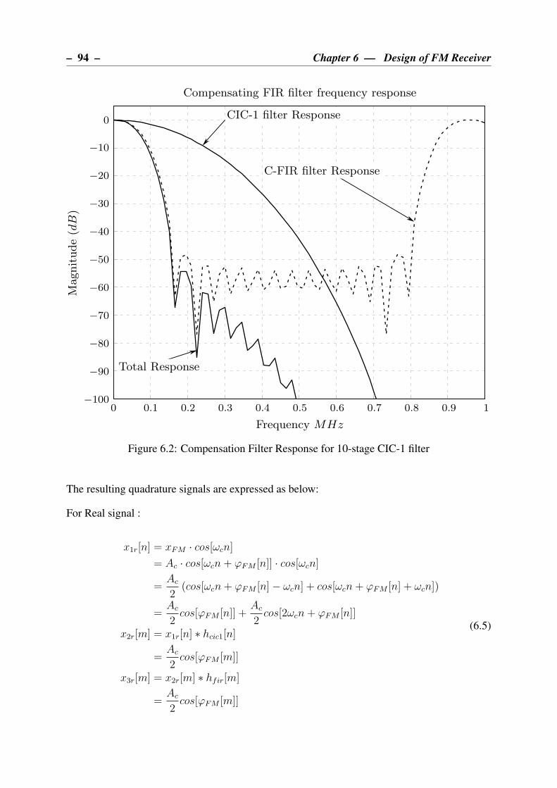
– 94 – Chapter 6 — Design of FM Receiver
0 0.1 0.2 0.3 0.4 0.5 0.6 0.7 0.8 0.9 1−100
−90
−80
−70
−60
−50
−40
−30
−20
−10
0
Frequency MHz
Magnitude(dB)
Compensating FIR filter frequency response
Total Response
CIC-1 filter Response
C-FIR filter Response
Figure 6.2: Compensation Filter Response for 10-stage CIC-1 filter
The resulting quadrature signals are expressed as below:
For Real signal :
x1r[n] = xFM · cos[ωcn]
= Ac · cos[ωcn+ ϕFM [n]] · cos[ωcn]
=Ac
2(cos[ωcn+ ϕFM [n]− ωcn] + cos[ωcn+ ϕFM [n] + ωcn])
=Ac
2cos[ϕFM [n]] +
Ac
2cos[2ωcn+ ϕFM [n]]
x2r[m] = x1r[n] ∗ hcic1[n]
=Ac
2cos[ϕFM [m]]
x3r[m] = x2r[m] ∗ hfir[m]
=Ac
2cos[ϕFM [m]]
(6.5)
Chapter 6 — Design of FM Receiver – 95 –
For Imaginary signal :
x1i[n] = xFM · sin[ωcn]
= Ac · cos[ωcn+ ϕFM [n]] · sin[ωcn]
=Ac
2(sin[−ωcn− ϕFM [n] + ωcn] + sin[ωcn+ ϕFM [n] + ωcn])
=Ac
2sin[−ϕFM [n]] +
Ac
2sin[2ωcn+ ϕFM [n]]
x2i[m] = −1 · x1i[n] ∗ hcic1[n]
=Ac
2sin[ϕFM [m]]
x3i[m] = x2i[m] ∗ hfir[m]
=Ac
2sin[ϕFM [m]]
(6.6)
where x1 is NCO output, x2 is CIC-1 output, x3 is a compensation FIR filter signal, hcic1 is
impulse response for CIC1 and hfir is impulse response for a compensation FIR filter.
At this stage, the RF signal has been down-converted to complex baseband I/Q signal. The
16-bit baseband I/Q samples are concatenated and then sent to a PC as 32-bit words using UDP.
At the PC end, FM demodulation is performed. The arctangent-differentiator [77] is chosen
because it more efficient than its I/Q demodulator counterparts. The arctan function recovers
the phase of the modulated signal followed by derivative of phase which yields the original
modulating message. Equation 6.7 shows how the demodulation process is done by using the
I/Q samples obtained from the last stage of the DDC core through 1 Gigabit Ethernet interface.
θdem = tan−1
[
x3i
x3r
]
= tan−1
Ac
2sin[ϕFM [m]]
Ac
2cos[ϕFM [m]]
= tan−1
sin[ϕFM [m]]
cos[ϕFM [m]]
= tan−1tan[ϕFM [m]]= ϕFM [m]
∆θdem[m] =d
dm
kvco
m−1∑
i=0
SM [m]
= kvco · SM [i]
(6.7)
6.2 DESIGN OF ANALOG RF FRONT-END
This section presents the design of an analogue RF front-end for the wideband FM receiver.
The block diagram of the frond-end design is shown in Figure 6.3. The indoor FM antenna with
a variable gain of 36dB receives -65dBm FM signal in the frequency range of 88-108MHz.
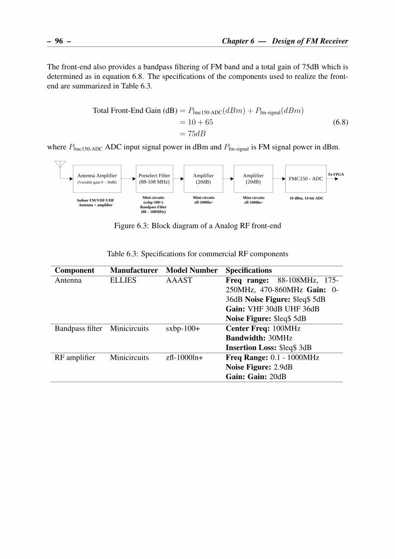
– 96 – Chapter 6 — Design of FM Receiver
The front-end also provides a bandpass filtering of FM band and a total gain of 75dB which is
determined as in equation 6.8. The specifications of the components used to realize the front-
end are summarized in Table 6.3.
Total Front-End Gain (dB) = Pfmc150-ADC(dBm) + Pfm-signal(dBm)
= 10 + 65
= 75dB
(6.8)
where Pfmc150-ADC ADC input signal power in dBm and Pfm-signal is FM signal power in dBm.
Antenna Amplifier(Variable gain 0 – 36dB)
Preselect Filter(88-108 MHz)
Amplifier(20dB)
Mini-circuitszfl-1000ln+
Mini-circuits(sxbp-100+)
Bandpass Filter(88 – 108MHz)
FMC150 - ADC
10 dBm, 14-bit ADCIndoor FM/VHF/UHF Antenna + amplifier
Amplifier (20dB)
Mini-circuitszfl-1000ln+
To FPGA
Figure 6.3: Block diagram of a Analog RF front-end
Table 6.3: Specifications for commercial RF components
Component Manufacturer Model Number Specifications
Antenna ELLIES AAAST Freq range: 88-108MHz, 175-
250MHz, 470-860MHz Gain: 0-
36dB Noise Figure: $leq$ 5dB
Gain: VHF 30dB UHF 36dB
Noise Figure: $leq$ 5dB
Bandpass filter Minicircuits sxbp-100+ Center Freq: 100MHz
Bandwidth: 30MHz
Insertion Loss: $leq$ 3dB
RF amplifier Minicircuits zfl-1000ln+ Freq Range: 0.1 - 1000MHz
Noise Figure: 2.9dB
Gain: Gain: 20dB

CHAPTER 7
RESULTS AND DISCUSSION
This chapter describes the tests that were carried out in order to ensure that the IP blocks were
designed and developed according to specified user requirements in section 3.1. The blocks
under test were designed in Chapter 4 and 5. The wideband FM receiver which was designed in
Chapter 6 using the developed IP blocks was also tested to demonstrate that developed library
can be reusable and reliably functional in the SDR context. All these tests will also provide
basis for conclusions and recommendations to be made in Chapter 8. The experimental setup
showing hardware and software tools used is shown in Figure 7.1.
DS03102A Oscilloscope
Waveform Generator
Desktop PC
Spectrum Analyzer
Power Supply
Analog RF frontend
RHINO Board Xilinx Platform
Cable USB
Indoor Antenna
(a)
Xilinx ISE Chipscope Pro Analyzer
Speedometer 2.8WiresharkISIM
simulator
(b)
Figure 7.1: Experimental environment showing Hardware and Software Tools use in this project
7.1 FIR CORE TEST
This section describes how the FIR IP core designed in section 4.1 was verified for its validity
using VHDL testbench and ISIM simulator. The results were plotted and compared to ideal
Matlab filter simulation results. The VHDL component of the core is provided in Appendix B.1
while the scripts are found in Appendix B.2 and B.3.
The FIR core was verified by designing length L = 95 FIR band-pass filter to specifications
97

– 98 – Chapter 7 — Results and Discussion
Table 7.1: Bandpass filter specifications generate FIR core coefficients
Parameter Value
Sampling frequency 10 kHz
Lower cutoff frequency 2190 Hz
Higher cutoff frequency 2215 Hz
Passband ripple 3 dB
Stopband attenuation 80 dB
Number of coefficients 95
shown in Table 7.1. The resulting Parks-McClellan optimal FIR coefficients of 16-bit width are
illustrated in Figure 7.3b in a form of filter frequency response. The filter was tested on an input
signal consisting of a sum of sinusoids at frequencies 440, 800, 2200 and 2500 Hz as shown in
Figure 7.3a. This input signal was created as vector of samples quantized to 16-bit precision
using Matlab script in Appendix B.2.
Table 7.2: FIR core parameter configurations
Parameter Value
DIN WIDTH 16
DOUT WIDTH 16
COEFF WIDTH 16
NUMBER OF TAPS 95
LATENCY 0
COEFFS A vector of filter response in
Figure 7.3b
clkrstwe
din [15..0]
BRAM
addr [15..0]
dout [15..0]
clkrstwe
din [31..0]
BRAM
addr [31..0]
dout [31..0]
clkrsten
din [15..0]
vld
FIR core
dout [31..0]loadc
coeff [15..0]
clk
rst
1
0
Figure 7.2: FIR core Testbench block diagram
To perform the experiment, the testbench was created as in Figure 7.2. The input signal stored in
memory was processed by the FIR core to single out the 2200Hz sinusoidal component shown
in Figure 7.3d. The result closely matches with the output of the ideal filter in Matlab shown in
Figure 7.3c. The SNR has of the output has slightly decreased due to quantization of coefficients
and results before and during core processing.
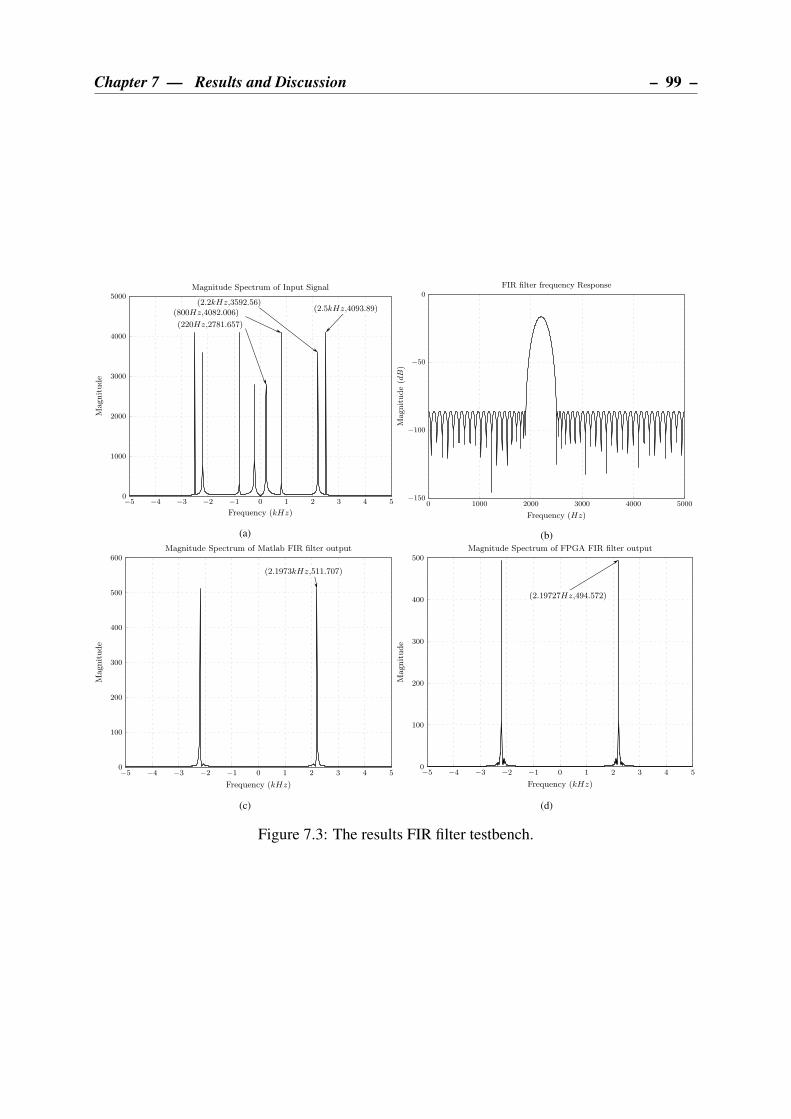
Chapter 7 — Results and Discussion – 99 –
−5 −4 −3 −2 −1 0 1 2 3 4 50
1000
2000
3000
4000
5000
Frequency (kHz)
Magnitude
Magnitude Spectrum of Input Signal
(220Hz,2781.657)
(800Hz,4082.006) (2.5kHz,4093.89)(2.2kHz,3592.56)
(a)
0 1000 2000 3000 4000 5000−150
−100
−50
0
Frequency (Hz)
Magnitude(dB)
FIR filter frequency Response
(b)
−5 −4 −3 −2 −1 0 1 2 3 4 50
100
200
300
400
500
600
Frequency (kHz)
Magnitude
Magnitude Spectrum of Matlab FIR filter output
(2.1973kHz,511.707)
(c)
−5 −4 −3 −2 −1 0 1 2 3 4 50
100
200
300
400
500
Frequency (kHz)
Magnitude
Magnitude Spectrum of FPGA FIR filter output
(2.19727Hz,494.572)
(d)
Figure 7.3: The results FIR filter testbench.

– 100 – Chapter 7 — Results and Discussion
7.2 IIR CORE TEST
This section outlines testing of IIR core designed in section 4.2. The aim was to demonstrate
the operation of high order IIR filter implemented with a cascade of second order sections
(SOS) and using VHDL tesbench and ISIM to verify IP core functionality and validity. The
coefficients were scaled as explained in section 4.2 to avoid overflow of results due to precision
of an FPGA. Matlab was used to generate input vector and to compare the IP core results with
ideal IIR simulation results of Matlab. All relevant Matlab scripts are provided in Appendix C.2
and C.3 whereas the VHDL component of the IIR core is provided in Appendix C.1.
Table 7.3: Bandpass filter specifications used to generate IIR core coefficients
Parameter Value
Sampling frequency 10 kHz
Lower cutoff frequency 2190 Hz
Higher cutoff frequency 2210 Hz
Passband ripple 0.1 dB
Stopband attenuation 200 dB
Number of coefficients 6
Number of sections 6
This filter testing was similar to the one in section 7.1 where the sum of sine waves 220, 800,
2200, 2500 Hz shown in Figure 7.5a were used as input vector to the IIR core and 2200Hz
sinusoid was isolated using a band-pass filter. The only difference is the filter specifications
used to generate coefficients for both FIR and IIR cores.
Table 7.4: IIR core parameter configurations
Parameter Value
DIN WIDTH 16
DOUT WIDTH 16
COEFF WIDTH 16
b A vector of filter response in
Figure 7.5b
a A vector of filter response in
Figure 7.5b
STAGES 6
The IIR filter response shown in Figure 7.5b was designed with Chebyshev Type I filter to spec-
ifications shown in Table 7.3 and IIR core parameters were configured as shown in Table 7.4.
The testbench of the experiment was setup as in Figure 7.4. Furthermore, the results of IIR
core obtained are shown in Figure 7.5d which closely match the ideal Matlab results shown in
Figure 7.5c.
Several observations were made when results obtained using FIR core in section 7.1 were com-
pared with results of IIR core in this section. The IIR filter is highly selective and it uses fewer
coefficients. This in turn led to improved results when IIR core was used.
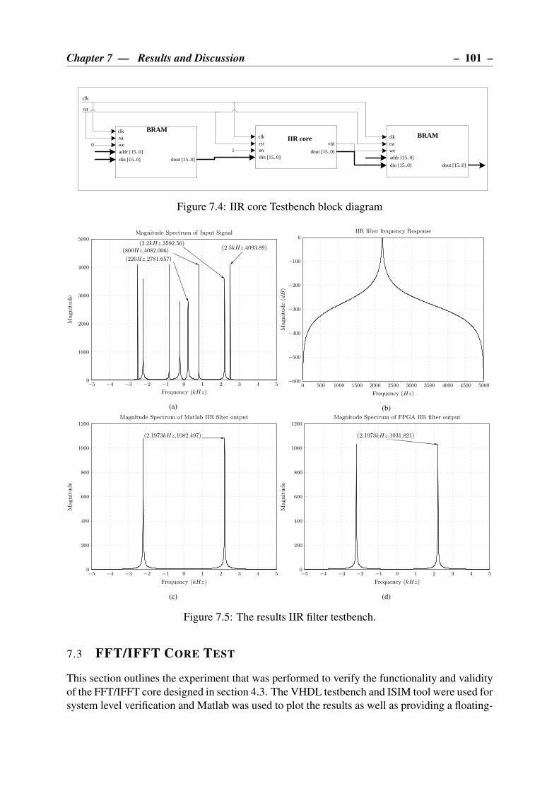
Chapter 7 — Results and Discussion – 101 –
clkrstwe
din [15..0]
BRAM
addr [15..0]
dout [15..0]
clkrstwe
din [15..0]
BRAM
addr [15..0]
dout [15..0]
clk
rst
clkrstendin [15..0]
vldIIR core
dout [15..0]10
Figure 7.4: IIR core Testbench block diagram
−5 −4 −3 −2 −1 0 1 2 3 4 50
1000
2000
3000
4000
5000
Frequency (kHz)
Magnitude
Magnitude Spectrum of Input Signal
(220Hz,2781.657)
(800Hz,4082.006) (2.5kHz,4093.89)(2.2kHz,3592.56)
(a)
0 500 1000 1500 2000 2500 3000 3500 4000 4500 5000−600
−500
−400
−300
−200
−100
0
Frequency (Hz)
Magnitude(dB)
IIR filter frequency Response
(b)
−5 −4 −3 −2 −1 0 1 2 3 4 50
200
400
600
800
1000
1200
Frequency (kHz)
Magnitude
Magnitude Spectrum of Matlab IIR filter output
(2.1973kHz,1082.497)
(c)
−5 −4 −3 −2 −1 0 1 2 3 4 50
200
400
600
800
1000
1200
Frequency (kHz)
Magnitude
Magnitude Spectrum of FPGA IIR filter output
(2.1973kHz,1031.821)
(d)
Figure 7.5: The results IIR filter testbench.
7.3 FFT/IFFT CORE TEST
This section outlines the experiment that was performed to verify the functionality and validity
of the FFT/IFFT core designed in section 4.3. The VHDL testbench and ISIM tool were used for
system level verification and Matlab was used to plot the results as well as providing a floating-

– 102 – Chapter 7 — Results and Discussion
point reference model for obtained results. The number of logic resources occupied by different
lengths of FFT core were recorded. The Matlab scripts used are provided in Appendix D.2 and
D.3 while the VHDL component of the FFT/IFFT core is provided in Appendix D.1.
For the most part, verification of the FFT/IFFT core was done using all supported N points
of the core at clock speed of 100MHz, however, only a 1024-point experiment will be demon-
strated in this section. Since the core operates in one of the two supported operating modes
namely FFT and IFFT mode, the experiment incorporates tests for both.
7.3.1 Testbench
The block diagram of a testbench is illustrated in Figure 7.6 and the generic parameters of
FFT/IFFT core were configured as in Table 7.5.
clk
rst
10
clkrsten
XSi [15..0]
vld
FFT/IFFT core
XKr [31..0]XSr [15..0]
XKi [31..0]
done
clkrstwe
dinr [15..0]
BRAM
addr [15..0]
douti [15..0]
doutr [15..0]dini [15..0]
clkrstwe
dinr [31..0]
BRAM
addr [15..0]
douti [31..0]
doutr [31..0]dini [31..0]
Figure 7.6: Testbench block diagram
Table 7.5: FFT/IFFT core configuration parameters as used in a testbench
Parameter Value
N 1024
DIN WIDTH 16
DOUT WIDTH 22
MODE 0=FFT,1=IFFT
The testbench environment involved generating a 1024 long input vector of a rectangular pulse
as shown in Figure 7.7a. This was used at the input to the core operating in FFT mode. The
output of the FFT core was stored in BRAM and later used as input data to the IFFT core whose
results were also kept in the final stage BRAM.
Moreover, the contents of both BRAMs were written to data files and plotted as shown in
Figure 7.7. The FFT core yielded the sinc waveform in Figure 7.7c which was the expected
fourier transform of a pulse waveform. This also matched with the Matlab generated FFT of the
pulse wave shown in Figure 7.7b. As expected, the IFFT core produced the original rectangular
pulse waveform which is illustrated in Figure 7.7d. However, the magnitude is vastly reduced
due to truncation of input word length that ensured the output values were kept below the 32-bit
fixed point limit when the values were growing in each pipeline stage of the FFT/IFFT core.
In order to allow the designer flexibly of choice with regard to FFT length and associated re-
source utilization, the synthesis report for all supported N-point FFT is provided in Table 7.6.

Chapter 7 — Results and Discussion – 103 –
0 5 10 15 200
10
20
30
40
Time (µs)
Amplitude(×
103)
Rectangular Pulse waveform
(a)
−20 −10 0 10 200
500
1000
1500
2000
Frequency (MHz)
Magnitude
1024-point FFT core output using MATLAB
(b)
−25 −20 −15 −10 −5 0 5 10 15 20 250
500
1000
1500
2000
Frequency (MHz)
Magnitude
1024-point FFT core output using FPGA
(c)
0 5 10 15 200
500
1000
1500
Time (µs)
Amplitude
1024-point IFFT core output using FPGA
(d)
Figure 7.7: MATLAB and FPGA results of a 1024-point FFT and IFFT core tested with rectan-
gular pulse input waveform.
These results were obtained using the same experiment setup as above but with differing lengths
of FFT and input vector.
7.3.2 Hardware Test
A similar experiment as in the previous section was performed to test the FFT/IFFT core but
this time the design needed to be fabricated on the FPGA. The input was still obtained from the
BRAM containing samples of a pulse waveform. Unlike previously where results were stored
in output in BRAM, the output samples were sent to a PC via Ethernet interface where results
were plotted and analysed. Although this type of testing is not a realistic SDR application, the
experiment was sufficient to verify the FFT/IFFT core functionality on the hardware and results
obtained were no different to the ones shown in Figure 7.7. A more sophisticated typical SDR
test experiment of the FFT/IFFT core is described later in section 7.6.3 of this chapter.
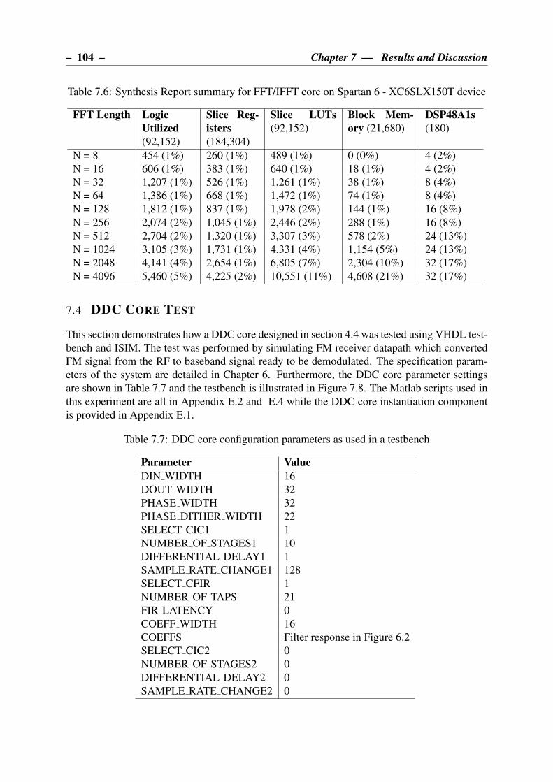
– 104 – Chapter 7 — Results and Discussion
Table 7.6: Synthesis Report summary for FFT/IFFT core on Spartan 6 - XC6SLX150T device
FFT Length Logic
Utilized
(92,152)
Slice Reg-
isters
(184,304)
Slice LUTs
(92,152)
Block Mem-
ory (21,680)
DSP48A1s
(180)
N = 8 454 (1%) 260 (1%) 489 (1%) 0 (0%) 4 (2%)
N = 16 606 (1%) 383 (1%) 640 (1%) 18 (1%) 4 (2%)
N = 32 1,207 (1%) 526 (1%) 1,261 (1%) 38 (1%) 8 (4%)
N = 64 1,386 (1%) 668 (1%) 1,472 (1%) 74 (1%) 8 (4%)
N = 128 1,812 (1%) 837 (1%) 1,978 (2%) 144 (1%) 16 (8%)
N = 256 2,074 (2%) 1,045 (1%) 2,446 (2%) 288 (1%) 16 (8%)
N = 512 2,704 (2%) 1,320 (1%) 3,307 (3%) 578 (2%) 24 (13%)
N = 1024 3,105 (3%) 1,731 (1%) 4,331 (4%) 1,154 (5%) 24 (13%)
N = 2048 4,141 (4%) 2,654 (1%) 6,805 (7%) 2,304 (10%) 32 (17%)
N = 4096 5,460 (5%) 4,225 (2%) 10,551 (11%) 4,608 (21%) 32 (17%)
7.4 DDC CORE TEST
This section demonstrates how a DDC core designed in section 4.4 was tested using VHDL test-
bench and ISIM. The test was performed by simulating FM receiver datapath which converted
FM signal from the RF to baseband signal ready to be demodulated. The specification param-
eters of the system are detailed in Chapter 6. Furthermore, the DDC core parameter settings
are shown in Table 7.7 and the testbench is illustrated in Figure 7.8. The Matlab scripts used in
this experiment are all in Appendix E.2 and E.4 while the DDC core instantiation component
is provided in Appendix E.1.
Table 7.7: DDC core configuration parameters as used in a testbench
Parameter Value
DIN WIDTH 16
DOUT WIDTH 32
PHASE WIDTH 32
PHASE DITHER WIDTH 22
SELECT CIC1 1
NUMBER OF STAGES1 10
DIFFERENTIAL DELAY1 1
SAMPLE RATE CHANGE1 128
SELECT CFIR 1
NUMBER OF TAPS 21
FIR LATENCY 0
COEFF WIDTH 16
COEFFS Filter response in Figure 6.2
SELECT CIC2 0
NUMBER OF STAGES2 0
DIFFERENTIAL DELAY2 0
SAMPLE RATE CHANGE2 0
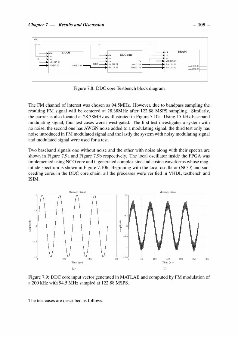
Chapter 7 — Results and Discussion – 105 –
clkrstwe
din [15..0]
BRAM
addr [15..0]
dout [15..0]
clk
rst
10
15136
clkrsten
din [15..0]
vld
DDC core
iout [31..0]ftw [31..0]
qout [31..0]
clkrstwe
dinr [31..0]
BRAM
douti [31..0]
doutr [31..0]dini [31..0]
addr [15..0]
Figure 7.8: DDC core Testbench block diagram
The FM channel of interest was chosen as 94.5MHz. However, due to bandpass sampling the
resulting FM signal will be centered at 28.38MHz after 122.88 MSPS sampling. Similarly,
the carrier is also located at 28.38MHz as illustrated in Figure 7.10a. Using 15 kHz baseband
modulating signal, four test cases were investigated. The first test investigates a system with
no noise, the second one has AWGN noise added to a modulating signal, the third test only has
noise introduced in FM modulated signal and the lastly the system with noisy modulating signal
and modulated signal were used for a test.
Two baseband signals one without noise and the other with noise along with their spectra are
shown in Figure 7.9a and Figure 7.9b respectively. The local oscillator inside the FPGA was
implemented using NCO core and it generated complex sine and cosine waveforms whose mag-
nitude spectrum is shown in Figure 7.10b. Beginning with the local oscillator (NCO) and suc-
ceeding cores in the DDC core chain, all the processes were verified in VHDL testbench and
ISIM.
0 100 200 300−1
−0.5
0
0.5
1
Time (µs)
Amplitude
Message Signal
(a)
0 50 100 150 200 250 300−1.5
−1
−0.5
0
0.5
1
1.5
Time (µs)
Amplitude
Message Signal
(b)
Figure 7.9: DDC core input vector generated in MATLAB and computed by FM modulation of
a 200 kHz with 94.5 MHz sampled at 122.88 MSPS.
The test cases are described as follows:

– 106 – Chapter 7 — Results and Discussion
−60 −40 −20 0 20 40 600
0.5
1
1.5
2
Frequency (MHz)
Magnitude(×
104)
Magnitude spectrum of a carrier
(28.38MHz,16384)
(a)
0 20 40 600
50
100
150
Frequency (MHz)
Magnitude
Magnitude spectrum of NCO
(28.38MHz,126)
(b)
Figure 7.10: A 28.38MHz carrier waveform generated in MATLAB and a local oscillator
28.38MHz signal generated by NCO core in FPGA.
7.4.1 Noise Free System Test
This test uses a noise free FM input signal shown in Figure 7.11a. In order to convert it to
baseband, NCO signals are multiplied with input FM signal using the mixer. The product of
this is desired signal component centred at DC and a spurious harmonic located at 56.76MHz
as shown in Figure 7.11b. This undesired signal component was removed by a CIC filter which
decimated the 122.88 MSPS ADC sample rate by a factor of 1:128 resulting in 960 kSPS sam-
ple rate as shown in Figure 7.11c. The non-ideal response of the CIC filter was corrected by
introducing a compensation FIR filter in the final stage of the DDC and its output is shown in
Figure 7.11d.
After the digital down conversion, the FM demodulator was used to demodulate the FM signal.
The magnitude spectrum and amplitude versus time graphs of the signal after demodulation
are shown in Figure 7.12a and 7.12b. This output has transient response which is the effect
of the FM demodulator. When the transient was removed and leaving only the steady state
response, this resulted in Magnitude spectrum and time domain graphs shown in Figure 7.12c
and 7.12d. The FM demodulated signal was compared to the original modulating signal shown
in Figure 7.11f and the results closely match.
7.4.2 Adding AWGN Noise to a Modulating Signal
After carrying out the first experiment without noise at the system input, a second one involved
adding 20dB AWGN to a 15kHz modulating signal shown in Figure 7.9b. This signal modulates
a pure 28.32MHz carrier in Figure 7.10a resulting in FM signal shown in Figure 7.13a. The FM
signal undergoes the same DDC core stages and finally the FM demodulator just as described
in section 7.4.1. The results are shown in Figure 7.13 and Figure 7.14.
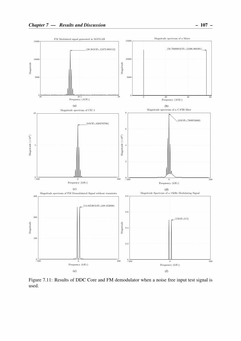
Chapter 7 — Results and Discussion – 107 –
28 28.5 290
5000
10000
15000
Frequency (MHz)
Magnitude
FM Modulated signal generated in MATLAB
(28.38MHz,12472.969112)
(a)
0 20 40 600
5000
10000
15000
Frequency (MHz)
Magnitude
Magnitude spectrum of a Mixer
(56.760000MHz,12496.960391)
(b)
−500 0 5000
5
10
Frequency (kHz)
Magnitude(×
108)
Magnitude spectrum of CIC-1
(0MHz,820270700)
(c)
−500 0 5000
2
4
6
8
Frequency (kHz)
Magnitude(×
108)
Magnitude spectrum of a C-FIR filter
(0MHz,789955600)
(d)
−500 0 5000
100
200
300
Frequency (kHz)
Magnitude
Magnitude spectrum of FM Demodulated Signal without transients
(14.845361kHz,249.452606)
(e)
−500 0 5000
0.2
0.4
0.6
0.8
Frequency (kHz)
Magnitude
Magnitude Spectrum of a 15kHz Modulating Signal
(15kHz,0.5)
(f)
Figure 7.11: Results of DDC Core and FM demodulator when a noise free input test signal is
used.
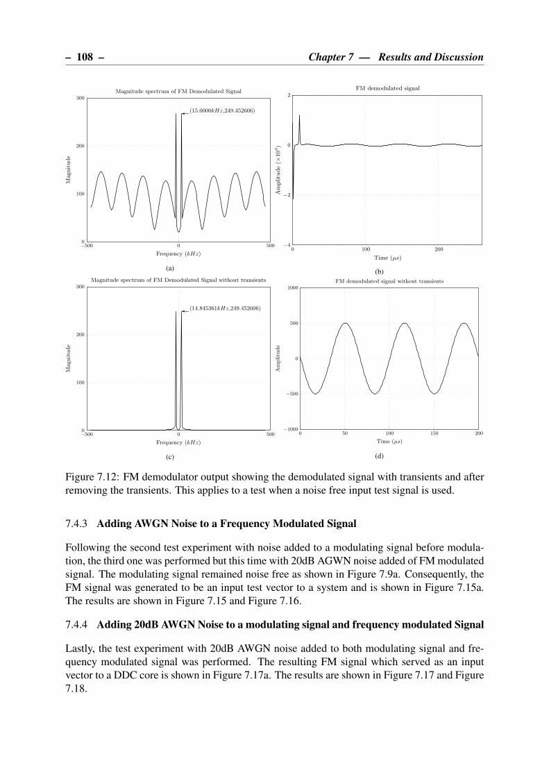
– 108 – Chapter 7 — Results and Discussion
−500 0 5000
100
200
300
Frequency (kHz)
Magnitude
Magnitude spectrum of FM Demodulated Signal
(15.0000kHz,249.452606)
(a)
0 100 200−4
−2
0
2
Time (µs)
Amplitude(×
104)
FM demodulated signal
(b)
−500 0 5000
100
200
300
Frequency (kHz)
Magnitude
Magnitude spectrum of FM Demodulated Signal without transients
(14.845361kHz,249.452606)
(c)
0 50 100 150 200−1000
−500
0
500
1000
Time (µs)
Amplitude
FM demodulated signal without transients
(d)
Figure 7.12: FM demodulator output showing the demodulated signal with transients and after
removing the transients. This applies to a test when a noise free input test signal is used.
7.4.3 Adding AWGN Noise to a Frequency Modulated Signal
Following the second test experiment with noise added to a modulating signal before modula-
tion, the third one was performed but this time with 20dB AGWN noise added of FM modulated
signal. The modulating signal remained noise free as shown in Figure 7.9a. Consequently, the
FM signal was generated to be an input test vector to a system and is shown in Figure 7.15a.
The results are shown in Figure 7.15 and Figure 7.16.
7.4.4 Adding 20dB AWGN Noise to a modulating signal and frequency modulated Signal
Lastly, the test experiment with 20dB AWGN noise added to both modulating signal and fre-
quency modulated signal was performed. The resulting FM signal which served as an input
vector to a DDC core is shown in Figure 7.17a. The results are shown in Figure 7.17 and Figure
7.18.
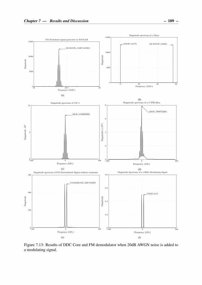
Chapter 7 — Results and Discussion – 109 –
28 28.5 290
5000
10000
15000
Frequency (MHz)
Magnitude
FM Modulated signal generated in MATLAB
(28.38MHz,12497.441981)
(a)
0 20 40 600
5000
10000
15000
Frequency (MHz)
Magnitude
Magnitude spectrum of a Mixer
(0MHz,33.77) (56.76MHz,12485)
(b)
−500 0 5000
5
10
Frequency (kHz)
Magnitude·108
Magnitude spectrum of CIC-1
(0kHz,819093300)
(c)
−500 0 5000
2
4
6
8
Frequency (kHz)
Magnitude(×
108)
Magnitude spectrum of a C-FIR filter
(0kHz,788875200)
(d)
−500 0 5000
100
200
300
Frequency (kHz)
Magnitude
Magnitude spectrum of FM Demodulated Signal without transients
(14.845361kHz,249.574287)
(e)
−500 0 5000
0.2
0.4
0.6
0.8
Frequency (kHz)
Magnitude
Magnitude Spectrum of a 15kHz Modulating Signal
(15kHz,0.5)
(f)
Figure 7.13: Results of DDC Core and FM demodulator when 20dB AWGN noise is added to
a modulating signal.

– 110 – Chapter 7 — Results and Discussion
−500 0 5000
100
200
300
Frequency (kHz)
Magnitude
Magnitude spectrum of FM Demodulated Signal
(15.0000kHz,267.971870)
(a)
0 100 200−4
−2
0
2
Time (µs)
Amplitude(×
104)
FM demodulated signal
(b)
−500 0 5000
100
200
300
Frequency (kHz)
Magnitude
Magnitude spectrum of FM Demodulated Signal without transients
(14.845361kHz,249.574287)
(c)
0 50 100 150 200−1000
−500
0
500
Time (µs)
Amplitude
FM demodulated signal without transients
(d)
Figure 7.14: FM demodulator output showing the demodulated signal with transients and after
removing the transients. This applies to a test where 20dB AWGN noise is added to a modulat-
ing signal.
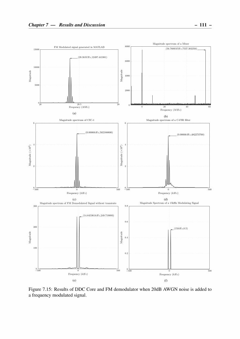
Chapter 7 — Results and Discussion – 111 –
28 28.5 290
5000
10000
15000
Frequency (MHz)
Magnitude
FM Modulated signal generated in MATLAB
(28.38MHz,12497.441981)
(a)
0 20 40 600
2000
4000
6000
8000
Frequency (MHz)
Magnitude
Magnitude spectrum of a Mixer
(56.7600MHz,7537.302256)
(b)
−500 0 5000
2
4
6
Frequency (kHz)
Magnitude(×
108)
Magnitude spectrum of CIC-1
(0.0000kHz,502188800)
(c)
−500 0 5000
2
4
6
Frequency (kHz)
Magnitude(×
108)
Magnitude spectrum of a C-FIR filter
(0.0000kHz,482273700)
(d)
−500 0 5000
100
200
300
Frequency (kHz)
Magnitude
Magnitude spectrum of FM Demodulated Signal without transients
(14.845361kHz,249.719093)
(e)
−500 0 5000
0.2
0.4
0.6
0.8
Frequency (kHz)
Magnitude
Magnitude Spectrum of a 15kHz Modulating Signal
(15kHz,0.5)
(f)
Figure 7.15: Results of DDC Core and FM demodulator when 20dB AWGN noise is added to
a frequency modulated signal.
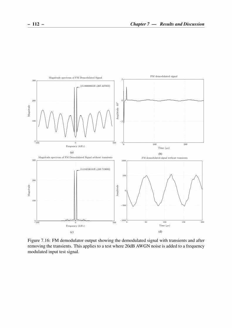
– 112 – Chapter 7 — Results and Discussion
−500 0 5000
100
200
300
Frequency (kHz)
Magnitude
Magnitude spectrum of FM Demodulated Signal
(15.000000kHz,267.427855)
(a)
0 100 200−4
−2
0
2
Time (µs)
Amplitude·104
FM demodulated signal
(b)
−500 0 5000
100
200
300
Frequency (kHz)
Magnitude
Magnitude spectrum of FM Demodulated Signal without transients
(14.845361kHz,249.719093)
(c)
0 50 100 150 200−1000
−500
0
500
1000
Time (µs)
Amplitude
FM demodulated signal without transients
(d)
Figure 7.16: FM demodulator output showing the demodulated signal with transients and after
removing the transients. This applies to a test where 20dB AWGN noise is added to a frequency
modulated input test signal.
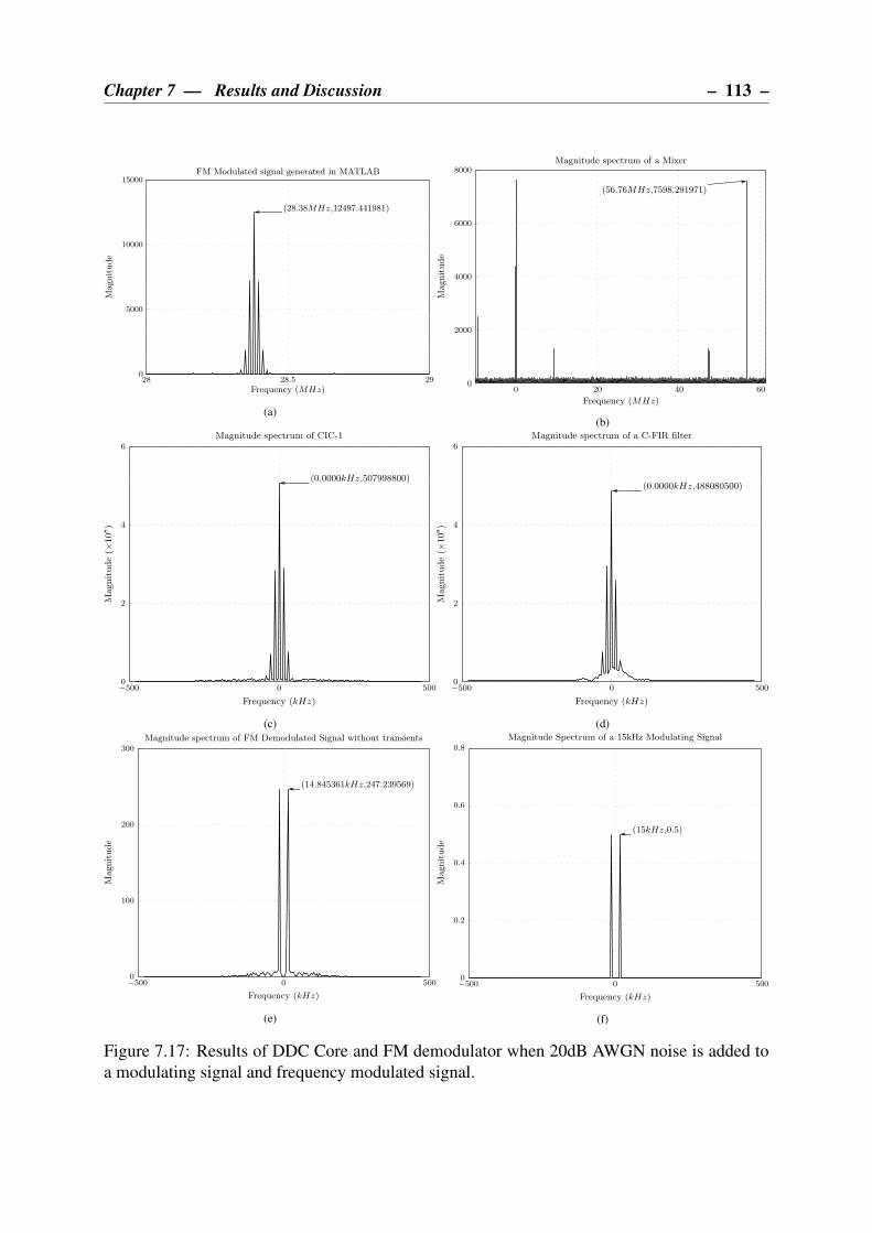
Chapter 7 — Results and Discussion – 113 –
28 28.5 290
5000
10000
15000
Frequency (MHz)
Magnitude
FM Modulated signal generated in MATLAB
(28.38MHz,12497.441981)
(a)
0 20 40 600
2000
4000
6000
8000
Frequency (MHz)
Magnitude
Magnitude spectrum of a Mixer
(56.76MHz,7598.291971)
(b)
−500 0 5000
2
4
6
Frequency (kHz)
Magnitude(×
108)
Magnitude spectrum of CIC-1
(0.0000kHz,507998800)
(c)
−500 0 5000
2
4
6
Frequency (kHz)
Magnitude(×
108)
Magnitude spectrum of a C-FIR filter
(0.0000kHz,488080500)
(d)
−500 0 5000
100
200
300
Frequency (kHz)
Magnitude
Magnitude spectrum of FM Demodulated Signal without transients
(14.845361kHz,247.239569)
(e)
−500 0 5000
0.2
0.4
0.6
0.8
Frequency (kHz)
Magnitude
Magnitude Spectrum of a 15kHz Modulating Signal
(15kHz,0.5)
(f)
Figure 7.17: Results of DDC Core and FM demodulator when 20dB AWGN noise is added to
a modulating signal and frequency modulated signal.

– 114 – Chapter 7 — Results and Discussion
−500 0 5000
100
200
300
Frequency (kHz)
Magnitude
Magnitude spectrum of FM Demodulated Signal
(15.000000kHz,265.902572)
(a)
0 100 200−4
−2
0
2
Time (µs)
Amplitude·104
FM demodulated signal
(b)
−500 0 5000
100
200
300
Frequency (kHz)
Magnitude
Magnitude spectrum of FM Demodulated Signal without transients
(14.845361kHz,247.239569)
(c)
0 50 100 150 200−1000
−500
0
500
1000
Time (µs)
Amplitude
FM demodulated signal without transients
(d)
Figure 7.18: FM demodulator output showing the demodulated signal with transients and after
removing the transients. This applies to a test where 20dB AWGN noise is added to a modulat-
ing signal and frequency modulated input test signal.

Chapter 7 — Results and Discussion – 115 –
7.5 UDP/IP CORE TEST
This section discusses the experiment that was performed to verify and evaluate performance
of a 1 Gigabit Ethernet interface using UDP/IP core designed in section 5.2. Its VHDL instan-
tiation component is provided in Appendix F.1. The experiment mainly put emphasis on data
transmission using both ARP and UDP protocols over a 1 Gigabit Ethernet. This proceeded by
establishing a peer to peer connection between a PC and RHINO as shown in Figure 3.6. A
physical connection was created by using a Cat5e UTP copper cable where one end connected
to 1Gbps network card on the PC and another end connected to a 1Gbps adapter or interface on
RHINO. The network parameters were configured as shown in Table 7.8.
Table 7.8: Point-to-Point Network configurations
Parameters RHINO (FPGA) Host PC
IP Address 192.168.0.3 192.168.0.1
MAC Address 00:24:ba:7d:1d:70 00:0c:29:3d:0d:2d
UDP port 9930 9930
The throughput speed was measured by sending multiple UDP packets of a fixed frame length
from the FPGA to a PC. In order to ensure maximum throughput speed and minimal packet
loss, each packet was sent whenever the UDP/IP core was fully ready to transmit data. A 1Hzsine waveform vector was used as payload in each UDP packet where the number of sine wave
samples equalled the UDP frame length.
The packets received on the PC were captured with a Command Line Tcpdump Linux tool and
Wireshark was used for analysis of captured packets. The outgoing packets only needed wire-
shark for monitoring. After data capture, the sine waveform vector in each frame was plotted to
verify that it was not corrupted during transmission in the physical link. Using wireshark, the
arrival times since the previous and the first packet were used to determine the amount of time
taken to transmit each packet and throughput speed as shown in equation 7.1.
Throughput Speed (MB/s) =Frame Length (bytes)× Number of Frames
Total Transmission Latency (seconds)(7.1)
Separate tests were made based on the direction of data flow between a PC and FPGA. Thus
data transfers were classified into two namely the upstream and downstream. Upstream refers
to transmission of UDP data from FPGA to a PC while the downstream is transmission of UDP
data from a PC to an FPGA. Before discussing test for both upstream and downstream, the ARP
test was performed and is described as follows:
7.5.1 ARP Test
The ARP communication packets were recorded as shown in Figure 7.19. As marked in this
figure using the first blue arrow, the FPGA sends a broadcast arp request to resolve unknown PC
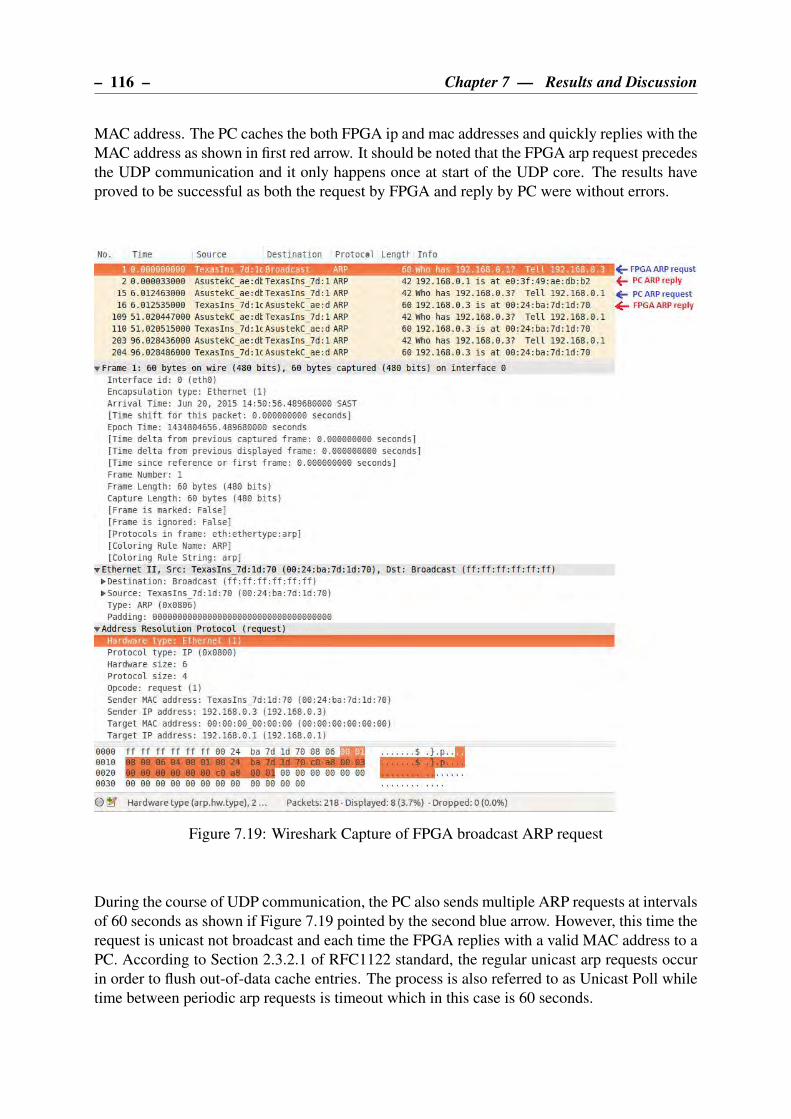
– 116 – Chapter 7 — Results and Discussion
MAC address. The PC caches the both FPGA ip and mac addresses and quickly replies with the
MAC address as shown in first red arrow. It should be noted that the FPGA arp request precedes
the UDP communication and it only happens once at start of the UDP core. The results have
proved to be successful as both the request by FPGA and reply by PC were without errors.
Figure 7.19: Wireshark Capture of FPGA broadcast ARP request
During the course of UDP communication, the PC also sends multiple ARP requests at intervals
of 60 seconds as shown if Figure 7.19 pointed by the second blue arrow. However, this time the
request is unicast not broadcast and each time the FPGA replies with a valid MAC address to a
PC. According to Section 2.3.2.1 of RFC1122 standard, the regular unicast arp requests occur
in order to flush out-of-data cache entries. The process is also referred to as Unicast Poll while
time between periodic arp requests is timeout which in this case is 60 seconds.
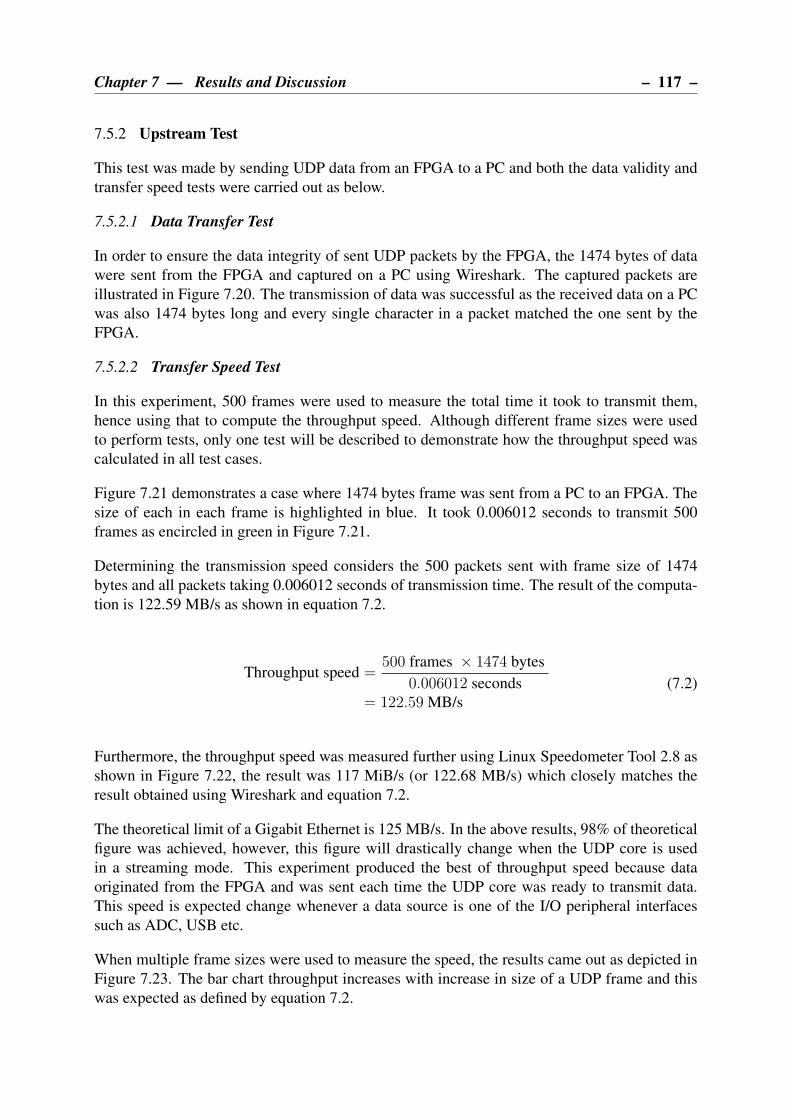
Chapter 7 — Results and Discussion – 117 –
7.5.2 Upstream Test
This test was made by sending UDP data from an FPGA to a PC and both the data validity and
transfer speed tests were carried out as below.
7.5.2.1 Data Transfer Test
In order to ensure the data integrity of sent UDP packets by the FPGA, the 1474 bytes of data
were sent from the FPGA and captured on a PC using Wireshark. The captured packets are
illustrated in Figure 7.20. The transmission of data was successful as the received data on a PC
was also 1474 bytes long and every single character in a packet matched the one sent by the
FPGA.
7.5.2.2 Transfer Speed Test
In this experiment, 500 frames were used to measure the total time it took to transmit them,
hence using that to compute the throughput speed. Although different frame sizes were used
to perform tests, only one test will be described to demonstrate how the throughput speed was
calculated in all test cases.
Figure 7.21 demonstrates a case where 1474 bytes frame was sent from a PC to an FPGA. The
size of each in each frame is highlighted in blue. It took 0.006012 seconds to transmit 500
frames as encircled in green in Figure 7.21.
Determining the transmission speed considers the 500 packets sent with frame size of 1474
bytes and all packets taking 0.006012 seconds of transmission time. The result of the computa-
tion is 122.59 MB/s as shown in equation 7.2.
Throughput speed =500 frames × 1474 bytes
0.006012 seconds
= 122.59 MB/s
(7.2)
Furthermore, the throughput speed was measured further using Linux Speedometer Tool 2.8 as
shown in Figure 7.22, the result was 117 MiB/s (or 122.68 MB/s) which closely matches the
result obtained using Wireshark and equation 7.2.
The theoretical limit of a Gigabit Ethernet is 125 MB/s. In the above results, 98% of theoretical
figure was achieved, however, this figure will drastically change when the UDP core is used
in a streaming mode. This experiment produced the best of throughput speed because data
originated from the FPGA and was sent each time the UDP core was ready to transmit data.
This speed is expected change whenever a data source is one of the I/O peripheral interfaces
such as ADC, USB etc.
When multiple frame sizes were used to measure the speed, the results came out as depicted in
Figure 7.23. The bar chart throughput increases with increase in size of a UDP frame and this
was expected as defined by equation 7.2.

– 118 – Chapter 7 — Results and Discussion
Figure 7.20: Trace of UDP traffic from FPGA showing the details of the UDP header
7.5.3 Downstream Test
Testing the downstream involved sending UDP data from the PC to an FPGA. In order to verify
if the packets are indeed arriving at the FPGA, the Chipscope Pro was used. Wireshark was
used to monitor the packets as they left the PC. Figure 7.24 shows as 37 bytes string encircled
in red which was sent to a PC at transmission rate of 35 MB/s. The string was captured on
FPGA and displayed on Chipscope Pro as illustrated in Figure 7.25.
Chapter 7 — Results and Discussion – 119 –
Figure 7.21: Trace of time taken for a single and 500 packets of UDP over 1Gbps Ethernet

– 120 – Chapter 7 — Results and Discussion
Figure 7.22: Measuring speed using Linux Speedometer Tool 2.8
0
10
20
30
40
50
60
70
80
90
100
110
120
10 18 34 64 130 258 514 1026 1102 1202 1402 1474
9.62
14.06
24.5
47.48
51.18
79.01
109.36
116.54 117.48119.94
121.15122.59
Frame Length (bytes)
Th
rou
gh
pu
t(M
B/s
)
Figure 7.23: Thoughput vs UDP Frame Length

Chapter 7 — Results and Discussion – 121 –
Figure 7.24: Trace of UDP packets being transmitted to FGPA over 1Gbps Ethernet
Figure 7.25: Capture of received UDP data on FPGA using ChipScope Pro
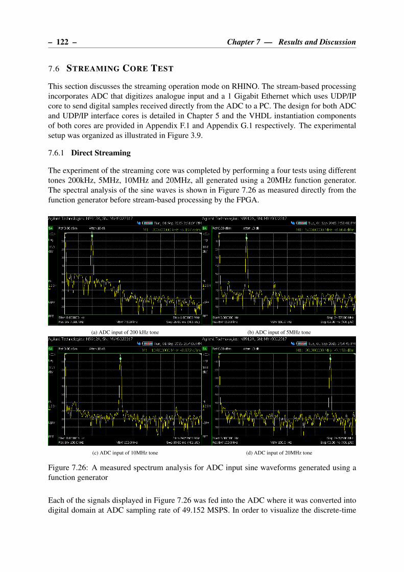
– 122 – Chapter 7 — Results and Discussion
7.6 STREAMING CORE TEST
This section discusses the streaming operation mode on RHINO. The stream-based processing
incorporates ADC that digitizes analogue input and a 1 Gigabit Ethernet which uses UDP/IP
core to send digital samples received directly from the ADC to a PC. The design for both ADC
and UDP/IP interface cores is detailed in Chapter 5 and the VHDL instantiation components
of both cores are provided in Appendix F.1 and Appendix G.1 respectively. The experimental
setup was organized as illustrated in Figure 3.9.
7.6.1 Direct Streaming
The experiment of the streaming core was completed by performing a four tests using different
tones 200kHz, 5MHz, 10MHz and 20MHz, all generated using a 20MHz function generator.
The spectral analysis of the sine waves is shown in Figure 7.26 as measured directly from the
function generator before stream-based processing by the FPGA.
(a) ADC input of 200 kHz tone (b) ADC input of 5MHz tone
(c) ADC input of 10MHz tone (d) ADC input of 20MHz tone
Figure 7.26: A measured spectrum analysis for ADC input sine waveforms generated using a
function generator
Each of the signals displayed in Figure 7.26 was fed into the ADC where it was converted into
digital domain at ADC sampling rate of 49.152 MSPS. In order to visualize the discrete-time
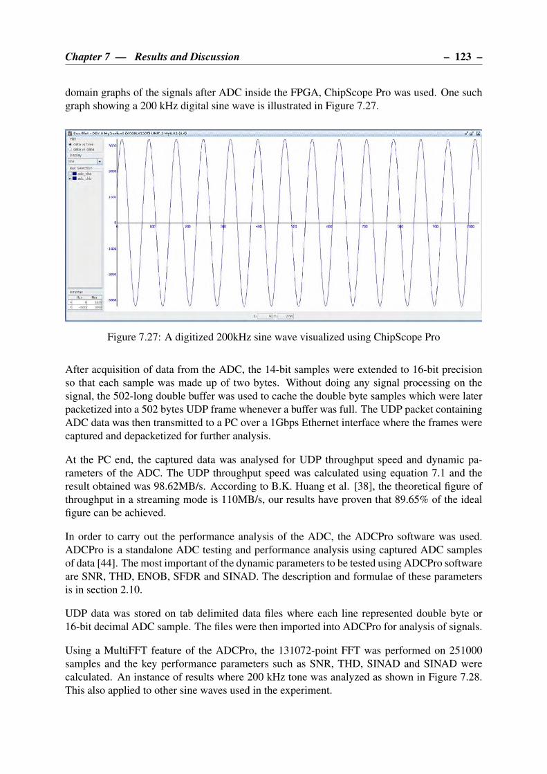
Chapter 7 — Results and Discussion – 123 –
domain graphs of the signals after ADC inside the FPGA, ChipScope Pro was used. One such
graph showing a 200 kHz digital sine wave is illustrated in Figure 7.27.
Figure 7.27: A digitized 200kHz sine wave visualized using ChipScope Pro
After acquisition of data from the ADC, the 14-bit samples were extended to 16-bit precision
so that each sample was made up of two bytes. Without doing any signal processing on the
signal, the 502-long double buffer was used to cache the double byte samples which were later
packetized into a 502 bytes UDP frame whenever a buffer was full. The UDP packet containing
ADC data was then transmitted to a PC over a 1Gbps Ethernet interface where the frames were
captured and depacketized for further analysis.
At the PC end, the captured data was analysed for UDP throughput speed and dynamic pa-
rameters of the ADC. The UDP throughput speed was calculated using equation 7.1 and the
result obtained was 98.62MB/s. According to B.K. Huang et al. [38], the theoretical figure of
throughput in a streaming mode is 110MB/s, our results have proven that 89.65% of the ideal
figure can be achieved.
In order to carry out the performance analysis of the ADC, the ADCPro software was used.
ADCPro is a standalone ADC testing and performance analysis using captured ADC samples
of data [44]. The most important of the dynamic parameters to be tested using ADCPro software
are SNR, THD, ENOB, SFDR and SINAD. The description and formulae of these parameters
is in section 2.10.
UDP data was stored on tab delimited data files where each line represented double byte or
16-bit decimal ADC sample. The files were then imported into ADCPro for analysis of signals.
Using a MultiFFT feature of the ADCPro, the 131072-point FFT was performed on 251000
samples and the key performance parameters such as SNR, THD, SINAD and SINAD were
calculated. An instance of results where 200 kHz tone was analyzed as shown in Figure 7.28.
This also applied to other sine waves used in the experiment.
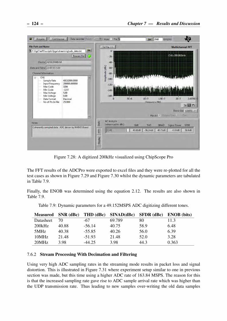
– 124 – Chapter 7 — Results and Discussion
Figure 7.28: A digitized 200kHz visualized using ChipScope Pro
The FFT results of the ADCPro were exported to excel files and they were re-plotted for all the
test cases as shown in Figure 7.29 and Figure 7.30 whilst the dynamic parameters are tabulated
in Table 7.9.
Finally, the ENOB was determined using the equation 2.12. The results are also shown in
Table 7.9.
Table 7.9: Dynamic parameters for a 49.152MSPS ADC digitizing different tones.
Measured SNR (dBc) THD (dBc) SINAD(dBc) SFDR (dBc) ENOB (bits)
Datasheet 70 -67 69.789 80 11.3
200kHz 40.88 -56.14 40.75 58.9 6.48
5MHz 40.38 -55.85 40.26 56.0 6.39
10MHz 21.48 -51.93 21.48 52.0 3.28
20MHz 3.98 -44.25 3.98 44.3 0.363
7.6.2 Stream Processing With Decimation and Filtering
Using very high ADC sampling rates in the streaming mode results in packet loss and signal
distortion. This is illustrated in Figure 7.31 where experiment setup similar to one in previous
section was made, but this time using a higher ADC rate of 163.84 MSPS. The reason for this
is that the increased sampling rate gave rise to ADC sample arrival rate which was higher than
the UDP transmission rate. Thus leading to new samples over-writing the old data samples
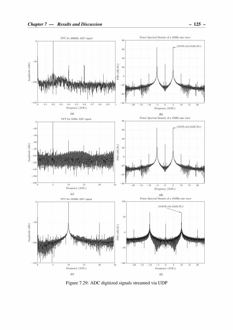
Chapter 7 — Results and Discussion – 125 –
0 0.1 0.2 0.3 0.4 0.5 0.6 0.7 0.8 0.9 1−150
−100
−50
0
Frequency (MHz)
Amplitude(dBc)
FFT for 200kHz ADC signal
(a)
−20 −15 −10 −5 0 5 10 15 20−60
−40
−20
0
20
40
60
80
Frequency (MHz)
PSD
(dB/Hz)
Power Spectral Density of a 5MHz sine wave
(5MHz,64.31dB/Hz)
(b)
0 5 10 15 20 25−180
−160
−140
−120
−100
−80
−60
−40
−20
0
Frequency (MHz)
Amplitude(dBc)
FFT for 5MHz ADC signal
(c)
−20 −15 −10 −5 0 5 10 15 20−60
−40
−20
0
20
40
60
80
Frequency (MHz)
PSD
(dB/Hz)
Power Spectral Density of a 5MHz sine wave
(5MHz,64.31dB/Hz)
(d)
0 5 10 15 20 25−150
−100
−50
0
Frequency (MHz)
Amplitude(dBc)
FFT for 10MHz ADC signal
(e)
−20 −15 −10 −5 0 5 10 15 20−100
−50
0
50
100
Frequency (MHz)
PSD
(dB/Hz)
Power Spectral Density of a 10MHz sine wave
(10MHz,64.12dB/Hz)
(f)
Figure 7.29: ADC digitized signals streamed via UDP

– 126 – Chapter 7 — Results and Discussion
0 5 10 15 20 25−100
−80
−60
−40
−20
0
20
Frequency (MHz)
Amplitude(dBc)
FFT for 20MHz ADC signal
(a)
−20 −10 0 10 20−100
−50
0
50
100
Frequency (MHz)
PSD
(dB/Hz)
Power Spectral Density of a 20MHz sine wave
(20MHz,64.18dB/Hz)
(b)
Figure 7.30: 20MHz tone ADC ouput streamed using UDP
awaiting UDP transmission in a buffer. Another reason was that UDP packets were sent to UDP
core faster than the Ethernet MAC could transmit the packets, hence leading to packets no being
sent to a PC at all.
Although it is also possible when using UDP that packets can be dropped at the receiver, in
this experiment it does not have much effect because the UDP/IP core is carefully designed
not to overwhelm the receiver with packets. As long as the throughput is kept below 125MB/s
the packet drops are negligible. The possibility of losing large volumes of data is when the
ADC sampling rate is too high resulting in buffer overflow before the UDP/IP core transmits
buffer data. This is a producer-consumer problem occurring inside the FPGA. Furthermore, the
corrupted packets can fail CRC that is enabled at the receiver. This can happen in noisy envi-
ronment or if a long Cat5e cable is used in a point-to-point network. However, these conditions
were avoided therefore packet drops were negligible as the CRC fails occurred infrequently.
To alleviate the shortcomings of a streaming core when high ADC sampling rates were used,
decimation and filtering were adopted in the design. Unlike the previous section where different
signal frequencies were tested, in this experiment only a 200kHz was used. The block diagram
of the setup is also illustrated in Figure 7.32. A very high 163.84 MSPS ADC sample rate was
chosen and decimated by a ratio of 1:32 which resulted in a 5.12 MSPS being used for UDP
transmission. A CIC decimation filter was used to perform downsampling and filtering, then
followed by a Compensation FIR filter which corrected non-flat response of a CIC filter.
The results showing the FFT and PSD of the ADC signal in the presence of CIC decimator and
Compensation FIR filter are depicted in Figure 7.33 and the resulting ADC dynamic parameters
proving improved results are shown in Table 7.10. As observed, the decimation and filtering
have a tremendous impact on the output signal. The reason being that they use relatively low
data rates on the DSP side to allow for sufficient transmission rate over Ethernet.

Chapter 7 — Results and Discussion – 127 –
−1 −0.8 −0.6 −0.4 −0.2 0 0.2 0.4 0.6 0.8 10
200
400
600
800
1000
1200
Frequency (MHz)
Magnitude
Magnitude Spectrum of a 200kHz sine wave
(a)
−1 −0.8 −0.6 −0.4 −0.2 0 0.2 0.4 0.6 0.8 1−20
0
20
40
60
80
Frequency (MHz)
PSD
(dB/Hz)
Power Spectral Density of a 200kHz sine wave
(b)
Figure 7.31: FPGA results of UDP streaming when 163.84MSPS ADC is used
1GbpsEthernet interface
1Gbps NIC
FPGA
PC
UDP communication
ADCFunction
Waveform Generator
ADC core
Compensation FIR Filter
CIC decimator
(1:32)
Figure 7.32: Experimental setup for stream-based processing with CIC decimation filter and
Compensation Filter
0 0.5 1 1.5 2 2.5−180
−160
−140
−120
−100
−80
−60
−40
−20
0
Frequency (MHz)
Amplitude(dBc)
FFT for 200kHz ADC signal
(a)
−2.5 −2 −1.5 −1 −0.5 0 0.5 1 1.5 2 2.5−20
0
20
40
60
Frequency (MHz)
PSD
(dB/Hz)
PSD of UDP signal
(0.2MHz,58dB/Hz)
(b)
Figure 7.33: FPGA results of UDP streaming when a CIC and FIR filters are used to process a
200 kHz signal sampled by the ADC at 163.84 MSPS

– 128 – Chapter 7 — Results and Discussion
Table 7.10: Dynamic parameters for a 163.84 MSPS ADC digitizing 200kHz tone. The ADC
sample rate is decimated resulting in sample rate of 5.12 MSPS prior to UDP transmission
Measured SNR (dBc) THD (dBc) SINAD (dBc) SFDR (dBc) ENOB (bits)
Datasheet 70 -67 69.789 80 11.3
200kHz 42.24 -73.35 42.24 73.4 6.72
7.6.3 Testing the FFT Core inside Streaming Logic
Having demonstrated the successful functionality of the streaming core, the FFT core was fur-
ther tested by placing it between the ADC core and UDP core so that it could perform FFT of
ADC digitized signals. Three tests that included 133kHz, 200kHz and 445kHz sine waveforms
were used and their FFTs were performed in separate tests. In each case, the FFT lengths of
512 and 4096 were used and the lowest 6.144 MSPS sample rate for ADC was used. However,
before the FFT experiment was carried out, the digital data of the three signals was captured
without the FFT core. The FFT of the each three sinusoid was determined and plotted using
Matlab. This served as an ideal reference model to the results processed using FFT core in
FPGA. Figure 7.34 shows the setup used for the experiment.
1GbpsEthernet interface
1Gbps NIC
FPGA
PC
UDP communication
ADCFunction
Waveform Generator
ADC core
FFT core
Figure 7.34: Experimental setup for FFT core as tested on the FPGA
The results of MATLAB FFT and FPGA FFT core are shown in Table 7.11 in a form of fre-
quency and the difference between two FFT lengths. The graphs of computed FFT in MATLAB
and FPGA for 133kHz, 200kHz and 445kHz ADC tones are shown in Figure 7.35, 7.36 and
7.37.
Table 7.11: MATLAB and FPGA FFT results of ADC sines waves streamed from FPGA via
UDP
MATLAB FFT frequency (kHz) FPGA FFT Core Frequency (kHz)
Signal N=512 N=4096 Difference N=512 N=4096 Difference
133kHz 132.000 133.500 1.5 132.000 133.500 1.5
200kHz 204.000 199.500 4.5 204.000 199.500 4.5
445kHz 444.000 445.500 1.5 444.000 445.500 1.5
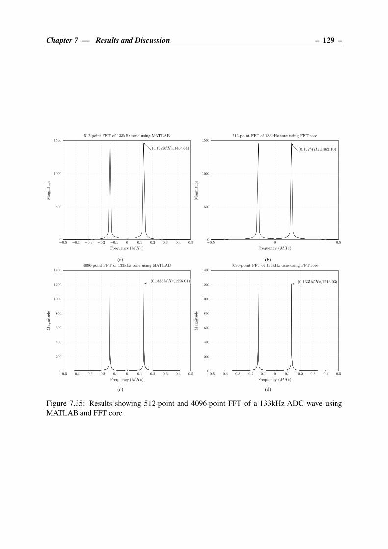
Chapter 7 — Results and Discussion – 129 –
−0.5 −0.4 −0.3 −0.2 −0.1 0 0.1 0.2 0.3 0.4 0.50
500
1000
1500
Frequency (MHz)
Magnitude
512-point FFT of 133kHz tone using MATLAB
(0.132MHz,1467.64)
(a)
−0.5 0 0.50
500
1000
1500
Frequency (MHz)
Magnitude
512-point FFT of 133kHz tone using FFT core
(0.132MHz,1462.10)
(b)
−0.5 −0.4 −0.3 −0.2 −0.1 0 0.1 0.2 0.3 0.4 0.50
200
400
600
800
1000
1200
1400
Frequency (MHz)
Magnitude
4096-point FFT of 133kHz tone using MATLAB
(0.1335MHz,1226.01)
(c)
−0.5 −0.4 −0.3 −0.2 −0.1 0 0.1 0.2 0.3 0.4 0.50
200
400
600
800
1000
1200
1400
Frequency (MHz)
Magnitude
4096-point FFT of 133kHz tone using FFT core
(0.1335MHz,1216.03)
(d)
Figure 7.35: Results showing 512-point and 4096-point FFT of a 133kHz ADC wave using
MATLAB and FFT core
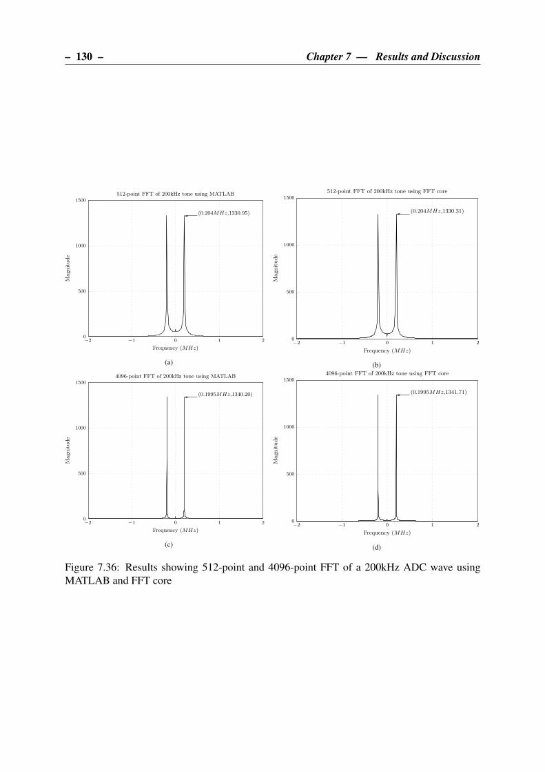
– 130 – Chapter 7 — Results and Discussion
−2 −1 0 1 20
500
1000
1500
Frequency (MHz)
Magnitude
512-point FFT of 200kHz tone using MATLAB
(0.204MHz,1330.95)
(a)
−2 −1 0 1 20
500
1000
1500
Frequency (MHz)
Magnitude
512-point FFT of 200kHz tone using FFT core
(0.204MHz,1330.31)
(b)
−2 −1 0 1 20
500
1000
1500
Frequency (MHz)
Magnitude
4096-point FFT of 200kHz tone using MATLAB
(0.1995MHz,1340.20)
(c)
−2 −1 0 1 20
500
1000
1500
Frequency (MHz)
Magnitude
4096-point FFT of 200kHz tone using FFT core
(0.1995MHz,1341.71)
(d)
Figure 7.36: Results showing 512-point and 4096-point FFT of a 200kHz ADC wave using
MATLAB and FFT core
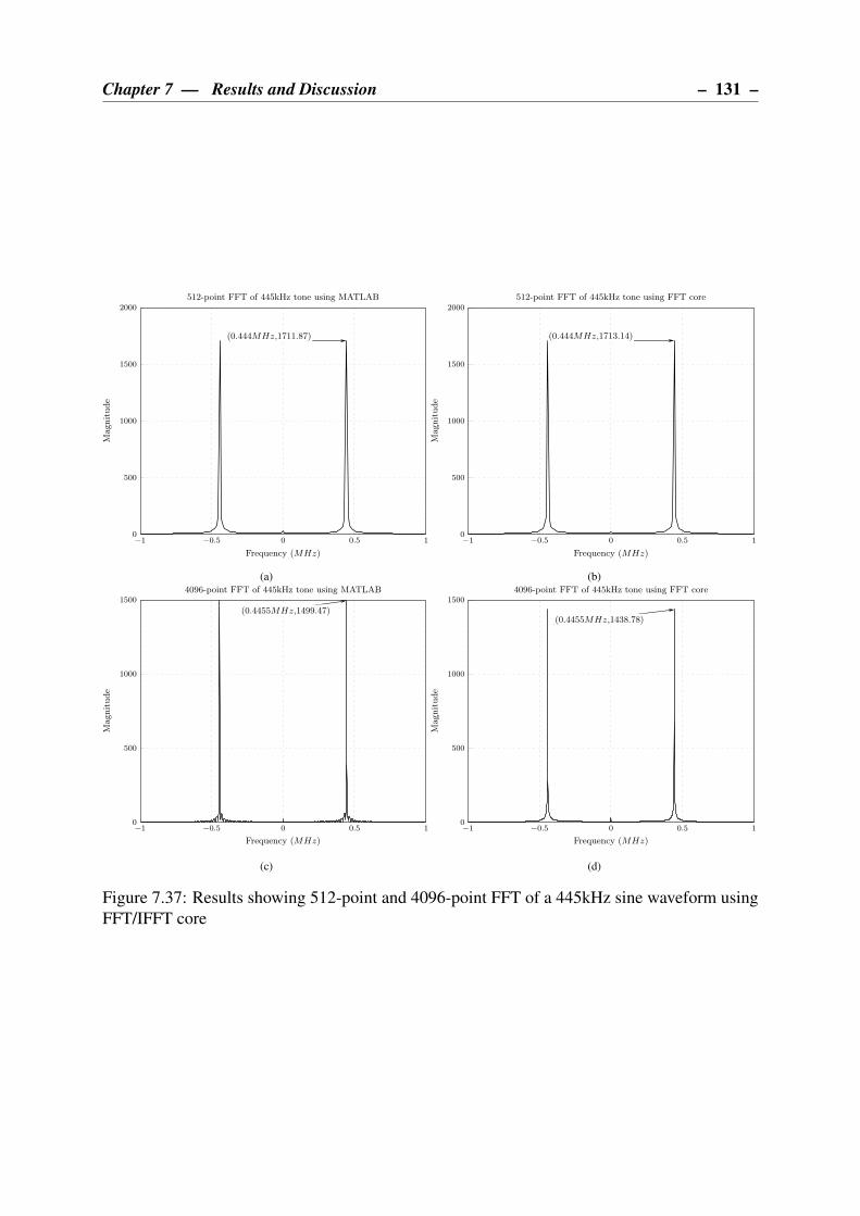
Chapter 7 — Results and Discussion – 131 –
−1 −0.5 0 0.5 10
500
1000
1500
2000
Frequency (MHz)
Magnitude
512-point FFT of 445kHz tone using MATLAB
(0.444MHz,1711.87)
(a)
−1 −0.5 0 0.5 10
500
1000
1500
2000
Frequency (MHz)
Magnitude
512-point FFT of 445kHz tone using FFT core
(0.444MHz,1713.14)
(b)
−1 −0.5 0 0.5 10
500
1000
1500
Frequency (MHz)
Magnitude
4096-point FFT of 445kHz tone using MATLAB
(0.4455MHz,1499.47)
(c)
−1 −0.5 0 0.5 10
500
1000
1500
Frequency (MHz)
Magnitude
4096-point FFT of 445kHz tone using FFT core
(0.4455MHz,1438.78)
(d)
Figure 7.37: Results showing 512-point and 4096-point FFT of a 445kHz sine waveform using
FFT/IFFT core
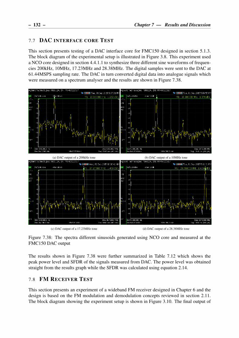
– 132 – Chapter 7 — Results and Discussion
7.7 DAC INTERFACE CORE TEST
This section presents testing of a DAC interface core for FMC150 designed in section 5.1.3.
The block diagram of the experimental setup is illustrated in Figure 3.8. This experiment used
a NCO core designed in section 4.4.1.1 to synthesize three different sine waveforms of frequen-
cies 200kHz, 10MHz, 17.23MHz and 28.38MHz. The digital samples were sent to the DAC at
61.44MSPS sampling rate. The DAC in turn converted digital data into analogue signals which
were measured on a spectrum analyser and the results are shown in Figure 7.38.
(a) DAC output of a 200kHz tone (b) DAC output of a 10MHz tone
(c) DAC output of a 17.23MHz tone (d) DAC output of a 28.38MHz tone
Figure 7.38: The spectra different sinusoids generated using NCO core and measured at the
FMC150 DAC output
The results shown in Figure 7.38 were further summarized in Table 7.12 which shows the
peak power level and SFDR of the signals measured from DAC. The power level was obtained
straight from the results graph while the SFDR was calculated using equation 2.14.
7.8 FM RECEIVER TEST
This section presents an experiment of a wideband FM receiver designed in Chapter 6 and the
design is based on the FM modulation and demodulation concepts reviewed in section 2.11.
The block diagram showing the experiment setup is shown in Figure 3.10. The final output of

Chapter 7 — Results and Discussion – 133 –
Table 7.12: Summary of DAC results for different tones
Tone (MHz) Fundamental Power
Level (dBm)
Highest Spurious
Power Level (dBm)
SFDR (dBc)
0.2 1.282 -32 33.288
10 1.374 -44 45.374
17.23 1.489 -52 53.489
28.38 -0.4194 -54 53.590
the FPGA were complex I/Q samples centered at DC. These samples were then demodulated in
Matlab using arctan/differentiation FM demodulator. The output of the FM demodulator is real-
valued signal. Results were then compared to an ideal FM radio baseband signal [22] depicted
in Figure 7.39. The spectral content of this signal is mono audio between 0 and 15kHz, the pilot
tone at 19kHz, the stereo audio between 23 and 53kHz, and RBDS at 57kHz.
Figure 7.39: A spectrum of a baseband FM station [22]
Testing was performed by tuning to three different FM stations displayed in Table 7.13. The
results showing the spectrum of the FM band measured at the antenna output and after filtering
and further amplification are shown in Figure 7.40a and 7.40b respectively. These results show
stations which were used for testing and are marked using respective FM station IDs.
Table 7.13: FM stations used for the FM receiver experiment
ID FM station Frequency
1 City Centre 89.0 MHz
2 KFM 94.5 MHz
3 Constantia Berg 95.3 MHz
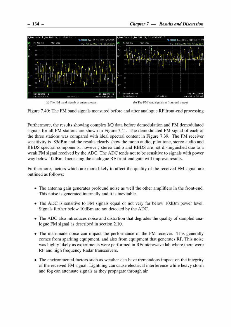
– 134 – Chapter 7 — Results and Discussion
(a) The FM band signals at antenna ouput (b) The FM band signals at front-end output
Figure 7.40: The FM band signals measured before and after analogue RF front-end processing
Furthermore, the results showing complex I/Q data before demodulation and FM demodulated
signals for all FM stations are shown in Figure 7.41. The demodulated FM signal of each of
the three stations was compared with ideal spectral content in Figure 7.39. The FM receiver
sensitivity is -85dBm and the results clearly show the mono audio, pilot tone, stereo audio and
RBDS spectral components, however; stereo audio and RBDS are not distinguished due to a
weak FM signal received by the ADC. The ADC tends not to be sensitive to signals with power
way below 10dBm. Increasing the analogue RF front-end gain will improve results.
Furthermore, factors which are more likely to affect the quality of the received FM signal are
outlined as follows:
• The antenna gain generates profound noise as well the other amplifiers in the front-end.
This noise is generated internally and it is inevitable.
• The ADC is sensitive to FM signals equal or not very far below 10dBm power level.
Signals further below 10dBm are not detected by the ADC.
• The ADC also introduces noise and distortion that degrades the quality of sampled ana-
logue FM signal as described in section 2.10.
• The man-made noise can impact the performance of the FM receiver. This generally
comes from sparking equipment, and also from equipment that generates RF. This noise
was highly likely as experiments were performed in RF/microwave lab where there were
RF and high frequency Radar transceivers.
• The environmental factors such as weather can have tremendous impact on the integrity
of the received FM signal. Lightning can cause electrical interference while heavy storm
and fog can attenuate signals as they propagate through air.

Chapter 7 — Results and Discussion – 135 –
−500 −400 −300 −200 −100 0 100 200 300 400 5000
5
10
15
20
Frequency (kHz)
Magnitude
Spectrum of 89.0MHz FM station (DDC core output)
(a)
0 10 20 30 40 50 60 700
0.005
0.01
0.015
Frequency (kHz)
Magnitude
Spectrum of FM demodulated 89.0MHz FM station in MATLAB
(b)
−500 −400 −300 −200 −100 0 100 200 300 400 5000
10
20
30
Frequency (kHz)
Magnitude
Spectrum of 94.5MHz FM station (DDC core output)
(c)
0 10 20 30 40 50 60 700
0.005
0.01
0.015
Frequency (kHz)
Magnitude
Spectrum of FM demodulated 94.5MHz FM station in MATLAB
(d)
−500 −400 −300 −200 −100 0 100 200 300 400 5000
5
10
15
Frequency (kHz)
Magnitude
Spectrum of 95.3MHz FM station (DDC core output)
(e)
0 10 20 30 40 50 60 700
0.005
0.01
0.015
Frequency (kHz)
Magnitude
Spectrum of FM demodulated 95.3MHz FM station in MATLAB
(f)
Figure 7.41: The results of FM Receiver when tuning to 89MHz, 94.5MHz and 95.3MHz sta-
tions

CHAPTER 8
CONCLUSIONS AND FURTHER WORK
This chapter presents the conclusions and future work for the SDR-based library of IP cores
proposed in this dissertation.
8.1 CONCLUSIONS
The developed library of IP blocks has passed all tests discussed in Chapter 7. This section
provides discussion and conclusions of the results obtained. The conclusions for the DSP IP
blocks will be presented first and this will be followed by conclusions relating to the I/O inter-
face blocks. Considerations for facilitating the reuse of these blocks by developers, in particular
novice developers that have little in the way of FPGA programming experience will be high-
lighted.
8.1.1 DSP IP blocks
The following processing IP blocks were chosen for inclusion into the DSP IP blocks library:
FIR filter, IIR filter, FFT/IFFT modules and a parameterized and highly scalable DDC block.
These cores were chosen specially in consideration of common SDR processing needs and this
selection was based on a thorough literature review as detailed in sections 2.3, 2.4 and 2.7.
Novice developers wanting to reuse these processing cores would consequently be advised to
review the theoretical operation of these blocks, possibly trying them in OCTAVE or MAT-
LAB to gain a practical understanding of their behavior or limits, whereafter they would be
familiar with the parameters concerned and be well prepared for moving to the FPGA, RHINO-
based context of application of making these processing operations work in a real environment.
Through the testing of these blocks done in this project, it was demonstrated in Chapter 7 that
the implementation of these blocks was successful and that they could be effectively connected
to other processing elements in the FPGA design to run in real time. These blocks were all
designed around a common SoC interface, namely Wishbone, which was done to further im-
prove the reusability of these blocks. In order to verify the functionality and correctness of these
blocks, testing which involved behavioural and functional simulation was performed.
FIR core experimental test was performed in section 7.1 and its results were compared to
high precision floating point results obtained using FIR simulation in Matlab. The comparison
demonstrated that the FPGA and Matlab results are almost in the same trend; however there still
136

Chapter 8 — Conclusions and Further Work – 137 –
exist some deviation which is a result of quantization noise and round-off noise. Furthermore,
not only was the FIR verified using behavioural and functional simulation, but the in-circuit
verification was also performed in section 7.6.2 where FIR core was used as the compensation
filter after decimation of high ADC sampling rate. This further justifies the extent of success to
which the FIR core was designed and tested.
The IIR core was tested in section 7.2 the same way as the FIR core but with different filter
design response. The results of the IIR core were similar to IIR simulation results in Matlab
and there was little deviation as seen when testing FIR core. The results of IIR core are more
improved because of high attenuation in the IIR filter stopband which is obtained with a smaller
number of coefficients in comparison to the FIR filter.
Testing of the FFT/IFFT core was also successful and was performed in section 7.3. The results
of the core operating as FFT and IFFT were compared with floating point FFT and IFFT func-
tions in Matlab and the results obtained were similar. Furthermore, the in-circuit verification
of the FFT/IFFT core was performed in a stream-based processing of ADC data as described
in section 7.6.3. The results obtained were compared with Matlab calculated FFT of ADC data
and were very similar to one another.
The DDC core was tested successfully using the FM signal which was created by modulating
94.5MHz carrier signal with 15kHz baseband signal as demonstrated in section 7.4. The FM
signal was processed by the DDC core and Digital FM demodulator. The final output was the
FM demodulated signal that had transients at the beginning but quickly faded away before the
system enters into a steady state. The steady state of FM demodulated signal was identical to the
original baseband 15kHz signal. The only small difference found was in the signal frequencies
which were calculated as 15kHz (original modulating signal) - 14.845361kHz (FM demodu-
lated signal) = 0.1546kHz. Furthermore, noise was added to the modulating signal and to FM
signal before DDC core processing and FM demodulation. The results obtained showed that
adding AWGN to modulating signal before modulation has no noticeable effect on the signal
produced after FM demodulation. On the hand, adding AWGN noise to the FM signal before
DDC core processing and FM demodulation results in reduced SNR of the output signal and
the AWGN noise is noticeable in the output signal.
8.1.2 I/O interface blocks
Testing of the I/O interface blocks involved in-circuit verification of UDP Ethernet IP core
and the FMC150 ADC/DAC sampling card interface core. Both of these interface blocks pro-
duced satisfactory results when tested on the RHINO board. In terms of novice engineers using
the capture card, there are preparatory and time-planning considerations for this: The 4DSP
FMC150 is a highly specialized card and has many configuration settings that need to be prop-
erly configured in order to make it operate in the way needed; while it is a powerful product
it is, from my experience, advisable for novice users to start with ready-made configuration
settings and one of the suggested RF bands in the tutorial before spending possibly days getting
the settings and the structure of the RF front-end circuitry properly aligned to the application
needs.
The UDP/IP core which created a reliable interface for 1 Gigabit Ethernet on RHINO was
– 138 – Chapter 8 — Conclusions and Further Work
tested first as discussed in section 7.5. The 1 Gigabit Ethernet testing was successful as UDP
data could be transferred in both directions and received on both the PC and FPGA without
errors. For novice developers wanting to experiment with prototyping their own SDR systems,
it would likely be easier, and likely work out quicker in the long run, were they to start with,
after initial OCTAVE/MATLAB experiments, to have a direct sampling core to Ethernet core
connection and work on maximizing the sample throughput of this arrangement, while doing
sanity checks on the RHINO’s output (to check for any breaks in data acquisition) and to test
algorithms on real data, before moving the processing operations (such as digital tuning and
FM demodulation) onto the FPGA using the pre-built DSP blocks.
The throughput speed of the 1 Gigabit Ethernet was tested with data generated within the FPGA
and the speed obtained was 122.59 MB/s which is 98% of theoretical 125 MB/s. However, when
1 Gigabit Ethernet was tested in a stream-based processing, the results dropped to 98.62 MB/s.
This is still a very good result as it is only 89.65% of the streaming mode theoretical figure of
110 MB/s. The range of UDP payload supported by the designed core ranges from 1 to 1474
bytes.
The results have demonstrated that very long packets of UDP data can be transferred between
the FPGA and the PC. Additionally, the practical throughput speed measured is very close to
the theoretical figure and this is a good sign that the designed UDP/IP core is performing as
expected. Some observations were made which will be important to take into consideration
when using the UDP/IP core. They are as follows:
• Very long UDP packets get corrupted or lost when sent to a PC at high transmission speed
using the 1 Gigabit Ethernet interface inside the FPGA. The reason for this is that packets
are dropped by PC network card due to high traffic bursts. This issue can be resolved by
increasing the receive buffer size in Linux Kernel. Another alternative is to reduce frame
size or the transmission speed.
• For stream-based processing using ADC and 1 Gigabit Ethernet, high ADC sampling
rates beyond 49.152MSPS lead to data loss between ADC interface core and UDP/IP.
An example showing results of this problem is illustrated in Figure 7.31. The reason for
this is that the arrival rate of ADC samples in the intermediary buffer is higher than the
transmission rate of UDP/IP core. The buffer fills up faster than the UDP/IP core gets
ready to transmit all values in the buffer and when it does, the new ADC samples will
have overwritten the old ones. To work around this problem, the digital down conversion
or decimation and filtering can be used as demonstrated in section 7.6.2.
• The throughput speed rises with an increase in frame size of UDP packet being transmit-
ted. Reducing the frame size minimizes the errors in the received packet by the PC.
FMC150 ADC/DAC interface core was the second I/O interface block to be tested where ADC
and DAC were tested separately. As fully described in section 7.6, ADC core was tested by
supplying an ADC with sine waves of different frequency generated by a function generator.
These analogue signals were converted to digital samples and then sent out to a PC as UDP
packets via 1 Gigabit Ethernet. At the PC end the ADC samples were captured and the ADC
Chapter 8 — Conclusions and Further Work – 139 –
dynamic parameters were measured using ADCPro software. The results were summarized
and compared to vendor-specified dynamic parameters as shown in Table 7.9. In all cases, the
SNR is relatively low in comparison with the datasheet figure. The reason for this is the phase
noise in the PLL generated clock that drives the ADC. SFDR, THD, SINAD and ENOB also
have lower values, the reason for this is pronounced spurious harmonics due to the high level
of distortion in the 10dBm input signal from a function generator. Using very low frequencies
improves the results whereas increasing the function generator frequency worsens the results.
The DAC core was also tested successfully in section 7.7 where NCO core was used to supply
the DAC with sine waves. The results obtained from the DAC output provided up to 53dBc of
SFDR. This SFDR increases with rise in frequency of the input signal to the DAC. Furthermore,
lower frequency signals have a number of spurious harmonics but they decrease when frequency
increases. This effect is due to phase quantization of the NCO core.
The last experiment performed was the FM receiver as described in section 7.8. The results
obtained were baseband I/Q data of received FM station and the FM demodulated signal of
the tuned FM station. The testing was performed using three FM stations and results were
successful. The spectra of the baseband I/Q signals represent typical FM modulated signals
while FM demodulated signals have the expected spectral components that include mono audio,
pilot tone, stereo audio and RBDS. The FM receiver sensitivity is -85dBm and the following
section 8.2, advises on ways to improve this due to limitations of the testing equipment used.
8.2 RECOMMENDATIONS FOR FURTHER WORK
This section presents some future refinements to the developed library of IP blocks for use in
SDR using RHINO as the development platform. Much work still remains for further improve-
ments in order to get a full package of IP blocks needed for SDR application development. The
IP blocks comprise both the DSP blocks and I/O interface blocks. The newly upgraded and
recommended architecture of RHINO SDR processing blocks is shown in Figure 8.1 with new
features labelled in italic red.
8.2.1 Upgrade the DSP blocks
The developed library of DSP IP cores was successful as it conforms to user requirements
defined in section 3.1. This library also presents fundamental DSP blocks from which other
more useful and robust DSP blocks can be built. Such blocks will also be compatible with
Wishbone bus and will be designed be around the following DSP algorithms:
• Polyphase Filterbank is a channelizer structure that implements a resource efficient
multichannel digital transmitter or receiver for a set of Frequency Division Multiplexed
(FDM) channels that exist in a single sampled data stream [106]. The IP core will be
realized using polyphase filterbank and it will be based on FFT IP core and FIR IP core
both designed in this project.
• Weighted Overlap Add Filter (WOLA) Filterbank is a channelization technique op-
timized for uniformly spaced channels with identical filtering [93]. The WOLA IP core
will be based on the FFT/IFFT IP core already designed in this dissertation.
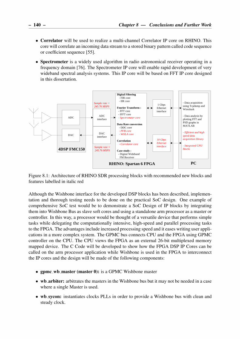
– 140 – Chapter 8 — Conclusions and Further Work
• Correlator will be used to realize a multi-channel Correlator IP core on RHINO. This
core will correlate an incoming data stream to a stored binary pattern called code sequence
or coefficient sequence [55].
• Spectrometer is a widely used algorithm in radio astronomical receiver operating in a
frequency domain [76]. The Spectrometer IP core will enable rapid development of very
wideband spectral analysis systems. This IP core will be based on FFT IP core designed
in this dissertation.
ADC interface
DAC interface
Digital Filtering - FIR core - IIR core
Fourier Transform : - FFT core - IFFT core - Spectrometer core
Data Rate conversion - DDC core - PFB core - WOLA core
Correlation - Correlator core
Case study : - Digital Wideband FM Receiver
1 Gbps Ethernet interface
- Data acquisition using Tcpdump and Wireshark
- Data analysis by plotting FFT and PSD graphs in MATLAB
- Efficient and high speed data acquisition library
- Integrated GNU blocks
ADC
DAC
PC
4DSP FMC150
RHINO: Spartan 6 FPGA
10 Gbps Ethernet interfaceSample rate =
245.76 MSPS
Sample rate = 245.76 MSPS
Figure 8.1: Architecture of RHINO SDR processing blocks with recommended new blocks and
features labelled in italic red
Although the Wishbone interface for the developed DSP blocks has been described, implemen-
tation and thorough testing needs to be done on the practical SoC design. One example of
comprehensive SoC test would be to demonstrate a SoC Design of IP blocks by integrating
them into Wishbone Bus as slave soft cores and using a standalone arm processor as a master or
controller. In this way, a processor would be thought of a versatile device that performs simple
tasks while delegating the computationally intensive, high-speed and parallel processing tasks
to the FPGA. The advantages include increased processing speed and it eases writing user appli-
cations in a more complex system. The GPMC bus connects CPU and the FPGA using GPMC
controller on the CPU. The CPU views the FPGA as an external 26-bit multiplexed memory
mapped device. The C Code will be developed to show how the FPGA DSP IP Cores can be
called on the arm processor application while Wishbone is used in the FPGA to interconnect
the IP cores and the design will be made of the following components:
• gpmc wb master (master 0): is a GPMC Wishbone master
• wb arbiter: arbitrates the masters in the Wishbone bus but it may not be needed in a case
where a single Master is used.
• wb sycon: instantiates clocks PLLs in order to provide a Wishbone bus with clean and
steady clock.

Chapter 8 — Conclusions and Further Work – 141 –
• wb intercon: ties up all wishbone components that include single master and multiple
slaves
• wb fir ip (slave 0): performs FIR filtering.
• wb fft ip (slave 1): performs FFT function of N = 8, 16, ...to4096.
• wb iir ip (slave 2): implements IIR filter structure using second-order sections IIR filter.
• wb ddc ip (slave 3): performs Digital down converter.
8.2.2 Improve the I/O interface blocks
The developed library of I/O interface blocks for 1 Gigabit Ethernet and FMC150 daughter
card worked successfully in accordance with requirements. However, some refinements are
needed in order to achieve the highest possible performance as specified by relevant standards
and vendors. For this reason, the following improvements are highly recommended for future
work:
• Perform a comprehensive loop back test for RHINO 1 Gigabit Ethernet on a point-to-
point connection with a PC. This will ensure that testing is thoroughly performed in both
directions of data flow between RHINO and a PC. In the current work, comprehensive
tests were performed in a flow of data from FPGA to a PC. Minor testing was performed
in sending of data from PC to an FPGA.
• While throughput speed achieved on 1 Gigabit Ethernet is sufficiently high particularly
for most SDR applications, this can still be improved from the current 98.62MB/s to a
figure closer to 110MB/s.
• The interface core for 10 Gigabit Ethernet also needs to be designed and implemented.
This will enable higher data rates not supported in 1 Gigabit Ethernet.
• Although RHINO provides interface for data communication at gigabit rates, the ineffi-
cient data acquisition at the PC end can be a massive speed bottleneck. For this reason,
a development of very efficient packet sniffing application on the PC is recommended.
This will capture packets at a high speed without packet loss and with no corruption of
received packet data.
• The development of a packet sniffing application will be integrated in GNU blocks for
real time DSP processing on the PC.
• The current maximum ADC sample rate achieved is 163.84MSPS while for DAC is
61.44MSPS. The sample rates for both ADC and DAC need to be improved to 245.76MSPS
using FMC150 daughter card.

– 142 – Chapter 8 — Conclusions and Further Work
8.2.3 Refine the FM receiver
The FM receiver worked successfully according to specifications, however; there is still room
for improvement to get even better results. This would be made possible by adding extra 30-
35dB amplifier and using a very efficient FM only antenna in the analogue RF front-end of the
FM receiver.
BIBLIOGRAPHY
[1] 4DSP. FMC150 User Manual. July 2013.
[2] ABOAGYE, A. K. Overflow avoidance techniques in cascaded iir filter implementations
on the tms320 dsp’s. Texas Instruments (5 1999).
[3] ABOAGYE, A. K. Overflow Avoidance Techniques in Cascaded IIR Filter Implementa-
tions on the TMS320 DSPs. spra509. Texas Instruments, 1999.
[4] AGHAEE, N., AND ESHGHI, M. Design of a pipelined r4sdf processor. 17th European
Signal Processing Conference (EUSIPCO 2009) (August 2009), 963–967.
[5] ALACHIOTIS, N., BERGER, S., AND STAMATAKIS, A. Efficient pc-fpga communica-
tion over gigabit ethernet. In Computer and Information Technology (CIT), 2010 IEEE
10th International Conference on (June 2010), pp. 1727–1734.
[6] ALACHIOTIS, N., BERGER, S., AND STAMATAKIS, A. A versatile udp/ip based pc -
fpga communication platform. In Reconfigurable Computing and FPGAs (ReConFig),
2012 International Conference on (Dec 2012), pp. 1–6.
[7] ALTERA. Understanding CIC Compensation Filters. apn455. Apr. 2007.
[8] ASHENDEN, P. J., AND LEWIS, J. The designers guide to VHDL, 3 ed. Morgan Kauf-
mann, 2008.
[9] AZARIAN, A., AND AHMADI, M. Reconfigurable computing architecture survey and
introduction. In Computer Science and Information Technology, 2009. ICCSIT 2009. 2nd
IEEE International Conference on (Aug 2009), pp. 269–274.
[10] BACKER, D., CHANG, C., CHAPMAN, D., CHEN, H., DROZ, P., DE JESUS, C.,
MACMAHON, D., SIEMION, A., WAWRZYNEK, J., WERTHIMER, D., AND WRIGHT,
M. A new approach to radio astronomy signal processing: Packet switched, fpga-based,
upgradable, modular hardware and reusable, platform-independent signal processing li-
braries. National Radio Science Meeting (2006).
[11] BAESE, M. Digital Signal Processing with Field Programmable Gate Arrays, 3 ed.
Berlin: Springer, 2007.
143
– 144 – BIBLIOGRAPHY
[12] BAKSHI, U. A., AND GODSE, A. P. Analog Communication, 2 ed. Technical Publica-
tions Prune, 2009.
[13] BOWLING, S. Understanding A/D Converter Performance Specifications. AN693. Mi-
crochip, 2000.
[14] BRANNON, B. Basics of Designing a Digital Radio Receiver (Radio 101). Analog
Devices.
[15] BRODERSEN, R., TKACHENKO, A., AND KWOK-HAY SO, H. A unified hardware/-
software runtime environment for fpga-based reconfigurable computers using borph. In
Hardware/Software Codesign and System Synthesis, 2006. CODES+ISSS ’06. Proceed-
ings of the 4th International Conference (Oct 2006), pp. 259–264.
[16] BURNS, P. Software Defined Radio for 3G. ARTECH HOUSE, 2003.
[17] CAICEDO, C. E. Software defined radio and software radio technology: Concepts
and applications. https://www.academia.edu/1319161/Software_
Defined_Radio_and_Software_Radio_Technology_Concepts_and_
Applications. Accessed: 2015-03-03.
[18] CANDILORO, D. Ip-core generator for the wishbone bus. http://www.dresd.
org/files/HPPS_Candiloro_2006_ENG.pdf, June 2006.
[19] COUSSY, P., BAGANNE, A., AND MARTIN, E. Ip cores integration in dsp system-
on-chip designs. In Signal Processing Conference, 2002 11th European (Sept 2002),
pp. 1–4.
[20] DAVIS, S. The need for thorough de-bugging capabilities in today’s multi-million gate
fpga designs is critical. http://www.usbid.com/datasheets/usbid/2000/
2000-q2/xl36_19.pdf. Accessed: 2015-03-04.
[21] DE A. MELO1, C. A. R., AND DE SOUZA2, R. E. Design and implementation of a
wishbonecompatible low-noise arbitrary waveform generator with dac compensation.
[22] DER, L. Frequency modulation (fm) tutorial. http://www.silabs.com/
Marcom%20Documents/Resources/FMTutorial.pdf. Accessed: 2015-08-
02.
[23] DESIGN, AND REUSE. Free ip cores projects. http://www.design-reuse.com/
download/sip/. Accessed: 2015-03-03.
[24] DONGYE, C. Design of the on-chip bus based on wishbone. In Electronics, Communi-
cations and Control (ICECC), 2011 International Conference on (Sept 2011), pp. 3653–
3656.
[25] FANG, F., HOE, J. C., PUSCHEL, M., AND MISRA, S. Generation of custom DSP trans-
form IP cores: Case study Walsh-Hadamard transform. In High Performance Embedded
Computing (HPEC) (2002).

BIBLIOGRAPHY – 145 –
[26] FOROUZAN, B. A., AND CHUNG, S. Data Communications and Networking 4th Edi-
tion, 4th ed. McGraw-Hill Higher Education, 2007.
[27] FRANCIS, M. Infinite Impulse Response Filter Structures in Xilinx FPGAs. WP330
(v1.2). Xilinx, Aug. 2009.
[28] GAD, V., GAD, R. S., AND NAIK, G. Implementation of gigabit ethernet standard using
fpga. International Journal of Mobile Network Communications & Telematics - IJMNCT
2, 4 (Aug. 2012), 31–44.
[29] GAISLER, J. A Dual-Use Open-Source VHDL IP library. Gaisler Research, 2004.
[30] GAJSKI, D., WU, A., CHAIYAKUL, V., MORI, S., NUKIYAMA, T., AND BRICAUD, P.
Essential issues for ip reuse. In Design Automation Conference, 2000. Proceedings of
the ASP-DAC 2000. Asia and South Pacific (June 2000), pp. 37–42.
[31] GAO, J. 10 100 1000 Mbps Tri-mode Ethernet MAC Specification. OpenCores, Jan.
2006.
[32] GHETIE, J. Fixed wireless and cellular mobile convergence: Technologies, solutions,
services. In Telecommunications, 2007. ConTel 2007. 9th International Conference on
(June 2007), pp. 343–343.
[33] GHIWALA, G. D., THAKER, P. P., AND D.AMIN, G. Realization of fpga based numeri-
cally controlled oscillator. IOSR Journal of VLSI and Signal Processing (IOSR-JVSP) 1,
5 (Jan-Feb 2013), 7–11.
[34] HE, S., AND TORKELSON, M. A new approach to pipeline fft processor. In Parallel
Processing Symposium, 1996., Proceedings of IPPS ’96, The 10th International (Apr
1996), pp. 766–770.
[35] HERVEILLE, R. Wishbone B4: WISHBONE System-on-Chip (SoC)Interconnection Ar-
chitecturefor Portable IP Cores. OpenCores, 2005.
[36] HOFNER, T. C. Measuring and evaluating Dynamic ADC parameters. Maxim Integrated
Products, Dec. 2000.
[37] HOSKING, R. H. Software Defined Radio Handbook. Pentek, One Park Way, upper
Saddle River, New Jersey 07458, Apr. 2012.
[38] HUANG, B. K., VANN, R. G. L., FREETHY, S., MYERS, R. M., NAYLOR, G.,
SHARPLES, R. M., AND SHEVCHENKO, V. F. Standardisation of fpga systems in-
corporating embedded linux: the mast ebw digitiser example. Fusion engineering and
design 87, 6 (Dec. 2012), 2106–2111.
[39] INGGS, G. Putting the pieces together: The systematic development of a software defined
radio toolflow for the rhino project. Master’s thesis, University Of Cape Town, May 2011.
[40] INSTRUMENTS, T. AMC7832 - Analog monitoring and control circuit. Mar. 2005.

– 146 – BIBLIOGRAPHY
[41] INSTRUMENTS, T. CDCE72010 - Ten Output High Performance Clock Synchronizer,
Jitter Cleaner, and Clock Distributor. June 2008.
[42] INSTRUMENTS, T. ads62p48/ads62p49/ads62p28/ads62p29 : Dual Channel 14-/12-Bit,
250-/210-MSPS ADC With DDR LVDS and Parallel CMOS Outputs. Apr. 2009.
[43] INSTRUMENTS, T. Dual-Channel, 16-Bit, 800 MSPS, Digital-to-Analog Converter
(DAC). Mar. 2010.
[44] INSTRUMENTS, T. ADCPro Hardware and Software Installation Manual. SLAU372A.
Feb. 2012.
[45] INSTRUMENTS, T. Design Consideration for Avoiding Timing Errors during High-Speed
ADC, LVDS Data Interface with FPGA. SLAA592A. June 2013.
[46] ITU. Transmission standards for FM sound broadcasting at VHF. Rec. ITU-R BS.450-3.
2001.
[47] JAIN, A. Verilog implementation of fpga based dsp design like fft processors. Xilinx
(1995).
[48] JEON, D., SEOK, M., CHAKRABARTI, C., BLAAUW, D., AND SYLVESTER, D.
Energy-optimized high performance fft processor. In Acoustics, Speech and Signal Pro-
cessing (ICASSP), 2011 IEEE International Conference on (May 2011), pp. 1701–1704.
[49] KESTER, W. The data conversion handbook. Analog Devices, 2005.
[50] KHALILZAD, N., YEKEH, F., ASPLUND, L., AND PORDEL, M. Fpga implementation
of real-time ethernet communication using rmii interface. In Communication Software
and Networks (ICCSN), 2011 IEEE 3rd International Conference on (May 2011), pp. 35–
39.
[51] KNAPP, S. Using Programmable Logic to Accelerate DSP Functions. Xilinx, Oct. 1995.
[52] KNAPP, S. K. Using programmable logic to accelerate dsp functions. Xilinx (1995).
[53] KOLUMBAN, G. Frequency modulation: Summary and repetition of the most impor-
tant facts, Mar 2015.
[54] KOZIEROK, C. The TCP/IP Guide: A Comprehensive, Illustrated Internet Protocols
Reference. No Starch Press, San Francisco, CA, USA, 2005.
[55] LATTICE. Correlator IP core. Lattice Semiconductor Corporation, Apr. 2005.
[56] LOPEZ-PARRADO, A., AND VALDERRAMA-CUERVO, J.-C. Openrisc-based system-
on-chip for digital signal processing. In Image, Signal Processing and Artificial Vision
(STSIVA), 2014 XIX Symposium on (Sept 2014), pp. 1–5.
[57] MADISETTI, V. K., AND WILLIAMS, D. B. Digital Signal Processing Handbook. CRC
Press, LLC, 1999.
BIBLIOGRAPHY – 147 –
[58] MAHMOODI, M., SAYEDI, S., AND MAHMOODI, B. Reconfigurable hardware imple-
mentation of gigabit udp/ip stack based on spartan-6 fpga. In Information Technology
and Electrical Engineering (ICITEE), 2014 6th International Conference on (Oct 2014),
pp. 1–6.
[59] MANOLAKIS, D., AND INGLE, V. Applied Digital Signal Processing. Cambridge Uni-
versity Press, 2011.
[60] MARVELL. 88E1111 Datasheet - Intergrated 10/100/1000 Ultra Ethernet Transceiver.
Dec. 2004.
[61] MIKROELECTRONIKA. Chapter 2: Fir filters - digital filter design. http://www.
mikroe.com/chapters/view/72/chapter-2-fir-filters/.
[62] MOHOR, I. Ethernet IP Core Specification. OpenCores, Nov. 2002.
[63] MOY, C., AND RAULET, M. High-level design methodology for ultra-fast software
defined radio prototyping on heterogeneous platforms. ADVANCES IN ELECTRONICS
AND TELECOMMUNICATIONS (Apr. 2010), 67–85.
[64] NEDERLAND, A. S. Designing fixed point direct form ii (biquad) iir filters with the asn
filter designer. Tech. rep., Advanced Solutions Nederland, Jan. 2012.
[65] OKADA, K., AND KOUSAI, S. Digitally-Assisted Analog and RF CMOS Circuit Design
for Software-Defined Radio. Springer Science+Business Media, 2011.
[66] OKLOBDZIJA, V. G. Computer Engineering HandBook. CRC Press LLC, 2002.
[67] OLIVIERI, S., AARESTAD, J., POLLARD, L., WYGLINSKI, A., KIEF, C., AND ERWIN,
R. Modular fpga-based software defined radio for cubesats. In Communications (ICC),
2012 IEEE International Conference on (June 2012), pp. 3229–3233.
[68] OLIVIERI, S. J., JIMAARESTAD, HOWARDPOLLARD, L., WYGLINSKI, A. M.,
CRAIGKIEF, AND ERWIN, R. S. Modular fpga-based software defined radio for cube-
sats. IEEE International Conference on Communications - Selected Areas in Communi-
cations Symposium (June 2012), 3229–3233.
[69] OPENCORES. Opencores projects. http://www.opencores.org/projects/.
Accessed: 2015-03-03.
[70] PANDA, A., BAGHMAR, S. K., AND AGRAWAL, S. K. Fir filter implementation on
a fpga allowing signed and fraction coefficients with coefficients obtained using remez
exchange algorithm. International Journal of Advancements in Technology 1 (2010),
203–210.
[71] PIMENTEL, J., AND LE-HUY, H. A vhdl library of ip cores for power drive and motion
control applications. In Electrical and Computer Engineering, 2000 Canadian Confer-
ence on (2000), vol. 1, pp. 184–188 vol.1.
[72] R, A., GANDHI, K., AND LAD, V. Low power r4sdc pipelined fft processor architecture.
IOSR Journal of VLSI and Signal Processing (IOSR-JVSP) 1, 6 (Mar-Apr 2013), 68–75.

– 148 – BIBLIOGRAPHY
[73] RAOL, K., KIML, D., AND HWANG, J. Fast Fourier Transform: Algorithms and Appli-
cations. Springer Dordrecht Heidelberg London New York, 2010.
[74] REDMON, N. Biquads. http://www.earlevel.com, Apr. 2003.
[75] REYES, P., REVIRIEGO, P., RUANO, O., AND MAESTRO, J. Efficient structures for the
implementation of moving average filters in the presence of seus using system knowl-
edge. the 2006 Radiation Effects on Components and Systems Workshop (Sept 2006).
[76] RF-ENGINES. RF Engines 1GHz Spectrometer Core drives unprecedented performance
enhancements in radio astronomy. RF Engines Ltd, Apr. 2005.
[77] RICE, M., PADILLA, M., AND NELSON, B. On fm demodulators in software defined ra-
dios using fpgas. In Military Communications Conference, 2009. MILCOM 2009. IEEE
(Oct 2009), pp. 1–7.
[78] ROUPHAEL, T. J. RF and Digital Signal Processing for Software-Defined Radio, A
Multi-Standard Multi-Mode Approach. Elsevier, 2009.
[79] RRSG. U.c.t remote radar sensign group - introducation. http://www.rrsg.uct.
ac.za/intro/intro.html. Accessed: 2015-08-20.
[80] RUDRA, A. Fpga-based applications for software radio. http://www.rfdesign.
com, Apr. 2004.
[81] SAEED, A., ELBABLY, M., ABDELFADEEL, G., AND ELADAWY, M. I. Efficient fpga
implementation of fft/ifft processor. International Journal of Circuits, Systems and Sig-
nal Processing 3 (2009).
[82] SALEH, R., WILTON, S., MIRABBASI, S., LEMIEUX, G., GRECU, C., IVANOV, A.,
HU, A., GREENSTREET, M., AND PANDE, P. P. System-on-chip: Reuse and integration.
Natural Sciences and Engineering Research Council of Canada (2010).
[83] SAVELA, V., JARVINEN, P., NUMMELA, A., KESKINEN, J., AND NURMI, J. Utiliza-
tion of a vhdl-based asic-realizable digital filter architecture library in dsp system design.
VIUF Proceedings (1994).
[84] SCHER, A. How to capture raw iq data from a rtl-sdr dongle and fm demodu-
late with matlab. http://www.aaronscher.com/wireless_com_SDR/RTL_
SDR_AM_spectrum_demod.html, May 2015. Accessed: 2015-08-06.
[85] SCHLICHTHARLE, D. Digital filters. Basics and design. 2nd ed., 2nd ed. ed. Berlin:
Springer, 2011.
[86] SCHWARZ, P. D. B. Iir filter design and implementation. Sep 2003.
[87] SCOTT, S. Rhino: Reconfigurable hardware interface for computation and radio. Mas-
ter’s thesis, University Of Cape Town, Nov. 2011.
[88] SDRG. Software defined radio group - university of cape town - electrical engineering.
http://www.sdrg.ee.uct.ac.za. Accessed: 2015-08-20.
BIBLIOGRAPHY – 149 –
[89] SENGAR, S., AND BHATTACHARYA, P. P. Performance evaluation of cascaded
integrator-comb (cic) filter. vol. 2, pp. 222–228.
[90] SHARMA, M., AND KUMAR, D. Wishbone bus architecture - a survey and comparison.
CoRR abs/1205.1860 (2012).
[91] SONG, W., AND LIU, B. Design of the cic decimation filter based on sopc builder. In
Computer Science and Information Technology (ICCSIT), 2010 3rd IEEE International
Conference on (July 2010), vol. 9, pp. 602–605.
[92] SPIRIDON, S. Software defined radio transceiver frontends in the beginning of the inter-
net era. COCORA: The Third International Conference on Advances in Cognitive Radio
(Apr. 2013), 18–22.
[93] TIETCHE, B., ROMAIN, O., DENBY, B., AND DIEULEVEULT, F. Fpga-based simulta-
neous multichannel fm broadcast receiver for audio indexing applications in consumer
electronics scenarios. Consumer Electronics, IEEE Transactions on 58, 4 (November
2012), 1153–1161.
[94] TRIBBLE, A. C. The software defined radio: Fact and fiction. IEEE Radio and Wireless
Symposium (Jan. 2008), 5–8.
[95] TSENG, S.-M., YU, J.-C., AND LIN, Z.-H. Software digital-down-converter design
and optimization for dvb-t systems. pp. 57–61.
[96] TUTTLEBE, W. H. W. Software- defined radio: Facets of a developing technology.
IEEE Personal Communications 6, 2 (Apr. 1999), 38–44.
[97] VAUGHAN, R., SCOTT, N., AND WHITE, D. The theory of bandpass sampling. Signal
Processing, IEEE Transactions on 39, 9 (Sept 1991), 1973–1984.
[98] VINOD, A., AND LAI, E. Low power and high-speed implementation of fir filters for
software defined radio receivers. Wireless Communications, IEEE Transactions on 5, 7
(July 2006), 1669–1675.
[99] WILLIAMS, J. Digilent atlys resources. https://www.joelw.id.au/FPGA/
DigilentAtlysResources. Accessed: 2015-08-02.
[100] WOODS, R., MCALLISTER, J., LIGHTBOY, G., AND YI, Y. FPGA-based Implementa-
tion of Complex Signal Processing Systems. John Wiley and Sons, Ltd, 2008.
[101] XILINX. Fpga design flow overview. http://www.xilinx.com/itp/
xilinx10/isehelp/ise_c_fpga_design_flow_overview.htm. Ac-
cessed: 2015-08-24.
[102] XILINX. LogiCORE IP Tri-Mode Ethernet MAC v4.5. UG138. Mar. 2011.
[103] XILINX. Spartan-6 Libraries Guide for HDL Designs. UG615. Mar. 2011.
[104] XILINX. LogiCORE IP AXI Ethernet Lite MAC (v1.01.b). DS787. July 2012.

– 150 – BIBLIOGRAPHY
[105] XILINX. LogiCORE IP Fast Fourier Transform v8.0. DS808. July 2012.
[106] XILINX. Polyphase Filter Bank Channelizer. XAPP1161. Mar. 2013.
[107] XILINX. Platform Cable USB II. DS593. Jan. 2015.

APPENDIX A
THE ATTACHED CD
The directory structure of the attached CD is described as follows:
• datasheets/ : This directory contains the datasheets for hardware components used in this
project.
• Java/ : This directory contains Netbeans project with Java files to implement depacketi-
zation of received UDP frames.
• Matlab/ : This directory contains the data files and Matlab files to plot the results.
• Msc Report TSNLEK001.pdf : This is a Thesis report file in PDF format.
• Pictures/ : This is a directory for experiment pictures.
• RHINO/ : This a directory for Xilinx ISe project which implements the entire library of
IP cores.
– RHINO/Rhino Sdr Blocks/pcores/ : This directory consists of all IP cores imple-
mented in VHDL using Xilinx ISE tools.
∗ DSP/ : The directory holds the developed DSP IP cores.
· CIC Lib/ : This is a directory that has all HDL files used to implement
CIC IP core. There also Matlab script files to help with testbench and
simulation.
· DDC Lib/ : The directory contains HDL files used to implement a DDC
IP core. It also contains Matlab script files needed for testbench and simu-
lation.
· FFT IFFT Lib/: This is directory with HDL files used to implement FFT/IFFT
IP core. The are also Matlab script files to help with testbench and simula-
tion.
· FIR Lib/ : This directory holds HDL files that implement FIR IP core and
Matlab script files use in testbench and simulation.
· IIR Lib/ : The directory consists of HDL files to realize IIR IP core and
Matlab script files for simulation and testench.
151
– 152 – Chapter A — The Attached CD
· NCO Lib/ : The directory holds HDL files that implement NCO core along
with Matlab script files to help with testbench and simulation.
· PRIMITIVES Lib/ : This directory has HDL entities commonly used in
many of the above developed cores.
∗ IO/: The directory holds the developed I/O interface cores.
· fmc150 if/ : This directory contains the HDL files for interfacing 4DSP
FMC150 ADC/DAC with RHINO.
· UDP 1GbE if/ : This directory has the HDL files for controlling and driv-
ing the 1 Gigabit Ethernet on RHINO.
∗ SDR/ : This directory contains the top level designs for developed DSP IP cores
and I/O interface cores.

APPENDIX B
FIR IP CORE
B.1 INSTANTIATION OF THE FIR CORE
1 Library FIR_Lib;
2 Use FIR_Lib.fir_pkg.all;
3 Use FIR_Lib.fircomponents.all;
4
5 -- FIR_PAR: A parallel implementation of an FIR filter,
6 -- it can be configured to operate in transpose form,
7 -- even symmetric form, odd symmetric form and as a
8 -- moving average filter.
9
10 fir_par_inst : fir_par
11 generic map(
12 DIN_WIDTH => DIN_WIDTH, -- input data width
13 DOUT_WIDTH => DOUT_WIDTH, -- output data width
14 COEFF_WIDTH => COEFF_WIDTH, -- coefficient data width
15 NUMBER_OF_TAPS => NUMBER_OF_TAPS,-- filter length
16 LATENCY => LATENCY, -- FIR structure type [0=tranpose, 1=odd
17 -- symmetric,2=even symmetric,3=moving average]
18 COEFFS => COEFFS -- array of quantized coefficients - integers
19 )
20 port map (
21 clk => clk, -- system clock input
22 rst => rst, -- system reset input
23 en => en, -- clock enable input
24 loadc => loadc, -- load coefficient enable input
25 vld => vld, -- valid output result
26 coeff => coeff, -- coefficient sample input
27 din => din, -- input data sample
28 dout => dout -- output data sample
29 );
B.2 GENERATING TESTBENCH DATA FILES IN MATLAB
1 % ----------------------------------------------------------------------
2 % This generates Parks-McClellan optimal FIR coefficients in 2’s
3 % complement and input test data for FPGA Testbench (fir_par.vhd core)
4 % ----------------------------------------------------------------------
5 %Lowpass Filter Design parameters
6 rp = 3; % passband ripple
7 rs = 100; % stopband ripple
8 Fs = 10000; % sampling frequency
9 f = [1905 2190 2215 2500]; % cutoff frequencies
10 a = [0 1 0]; % desired amplitudes
11 % compute deviations
153
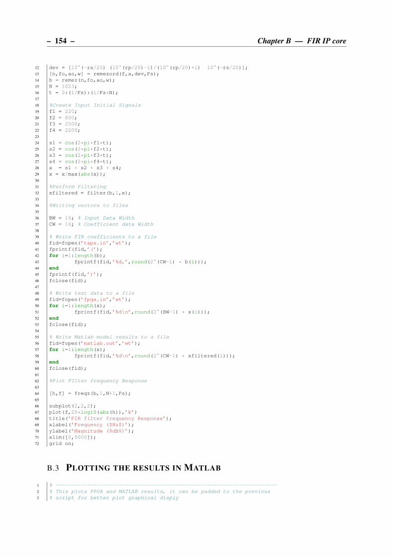
– 154 – Chapter B — FIR IP core
12 dev = [10ˆ(-rs/20) (10ˆ(rp/20)-1)/(10ˆ(rp/20)+1) 10ˆ(-rs/20)];
13 [n,fo,ao,w] = remezord(f,a,dev,Fs);
14 b = remez(n,fo,ao,w);
15 N = 1023;
16 t = 0:(1/Fs):(1/Fs*N);
17
18 %Create Input Initial Signals
19 f1 = 220;
20 f2 = 800;
21 f3 = 2500;
22 f4 = 2200;
23
24 s1 = cos(2*pi*f1*t);
25 s2 = cos(2*pi*f2*t);
26 s3 = cos(2*pi*f3*t);
27 s4 = cos(2*pi*f4*t);
28 x = s1 + s2 + s3 + s4;
29 x = x/max(abs(x));
30
31 %Perform Filtering
32 xfiltered = filter(b,1,x);
33
34 %Writing vectors to files
35
36 BW = 16; % Input Data Width
37 CW = 16; % Coefficient data Width
38
39 % Write FIR coefficients to a file
40 fid=fopen(’taps.in’,’wt’);
41 fprintf(fid,’(’);
42 for i=1:length(b);
43 fprintf(fid,’%d,’,round(2ˆ(CW-1) * b(i)));
44 end
45 fprintf(fid,’)’);
46 fclose(fid);
47
48 % Write test data to a file
49 fid=fopen(’fpga.in’,’wt’);
50 for i=1:length(x);
51 fprintf(fid,’%d\n’,round(2ˆ(BW-1) * x(i)));
52 end
53 fclose(fid);
54
55 % Write Matlab model results to a file
56 fid=fopen(’matlab.out’,’wt’);
57 for i=1:length(x);
58 fprintf(fid,’%d\n’,round(2ˆ(CW-1) * xfiltered(i)));
59 end
60 fclose(fid);
61
62 %Plot FIlter frequency Response
63
64 [h,f] = freqz(b,1,N+1,Fs);
65
66 subplot(2,2,2);
67 plot(f,20*log10(abs(h)),’k’)
68 title(’FIR filter frequency Response’);
69 xlabel(’Frequency ($Hz$)’);
70 ylabel(’Magnitude ($dB$)’);
71 xlim([0,5000]);
72 grid on;
B.3 PLOTTING THE RESULTS IN MATLAB
1 % ----------------------------------------------------------------------
2 % This plots FPGA and MATLAB results, it can be padded to the previous
3 % script for better plot graphical disply

Chapter B — FIR IP core – 155 –
4 % ----------------------------------------------------------------------
5 NFFT = 1024;
6 Ts = 1/Fs; % sampling interval
7 f = Fs*(-NFFT/2:NFFT/2-1)/NFFT; % frequency
8
9 fid = fopen(’fpga.in’);
10 fpgain = textscan(fid,’%f’,’Delimiter’,’\n’);
11 fclose(fid);
12
13 fid = fopen(’fpga.out’);
14 fpgaout = textscan(fid,’%f’,’Delimiter’,’\n’);
15 fclose(fid);
16
17 fid = fopen(’matlab.out’);
18 matlabout = textscan(fid,’%f’,’Delimiter’,’\n’);
19 fclose(fid);
20
21 % normalized FFT of signals
22 f1 = fftshift(fft(fpgain1,NFFT));
23 F1 = abs(f1)/(N);
24 f2 = fftshift(fft(matlabout1,NFFT));
25 F2 = abs(f2)/(N);
26 f3 = fftshift(fft(fpgaout1,NFFT));
27 F3 = abs(f3)/(N);
28
29 % FFT for FIR Testebech input signal
30 subplot(2,2,1);
31 plot(f/1e3,F1,’k’);
32 title(’Magnitude Spectrum of Input Signal’);
33 xlabel(’Frequency ($kHz$)’);
34 ylabel(’Magnitude’);
35 xlim([-5,5]);
36 grid on;
37
38 % FFT for MATLAB FIR output
39 subplot(2,2,3);
40 plot(f/1e3,F2,’k’);
41 title(’Magnitude Spectrum of Matlab FIR filter output’);
42 xlabel(’Frequency ($kHz$)’);
43 ylabel(’Magnitude’);
44 xlim([-5,5]);
45 grid on;
46
47 % FFT for FPGA FIR core output
48 subplot(2,2,4);
49 plot(f/1e3,F3,’k’);
50 title(’Magnitude Spectrum of FPGA FIR filter output’);
51 xlabel(’Frequency ($kHz$)’);
52 ylabel(’Magnitude’);
53 xlim([-5,5]);
54 grid on;
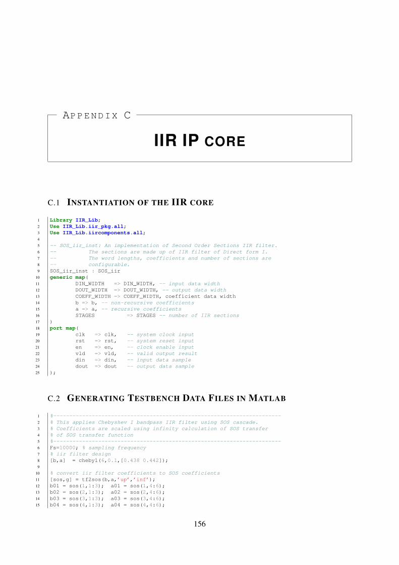
APPENDIX C
IIR IP CORE
C.1 INSTANTIATION OF THE IIR CORE
1 Library IIR_Lib;
2 Use IIR_Lib.iir_pkg.all;
3 Use IIR_Lib.iircomponents.all;
4
5 -- SOS_iir_inst: An implementation of Second Order Sections IIR filter.
6 -- The sections are made up of IIR filter of Direct form I.
7 -- The word lengths, coefficients and number of sections are
8 -- configurable.
9 SOS_iir_inst : SOS_iir
10 generic map(
11 DIN_WIDTH => DIN_WIDTH, -- input data width
12 DOUT_WIDTH => DOUT_WIDTH, -- output data width
13 COEFF_WIDTH => COEFF_WIDTH, coefficient data width
14 b => b, -- non-recursive coefficients
15 a => a, -- recursive coefficients
16 STAGES => STAGES -- number of IIR sections
17 )
18 port map(
19 clk => clk, -- system clock input
20 rst => rst, -- system reset input
21 en => en, -- clock enable input
22 vld => vld, -- valid output result
23 din => din, -- input data sample
24 dout => dout -- output data sample
25 );
C.2 GENERATING TESTBENCH DATA FILES IN MATLAB
1 %-----------------------------------------------------------------------
2 % This applies Chebyshev I bandpass IIR filter using SOS cascade.
3 % Coefficients are scaled using infinity calculation of SOS transfer
4 % of SOS transfer function
5 %-----------------------------------------------------------------------
6 Fs=10000; % sampling frequency
7 % iir filter design
8 [b,a] = cheby1(6,0.1,[0.438 0.442]);
9
10 % convert iir filter coefficients to SOS coefficients
11 [sos,g] = tf2sos(b,a,’up’,’inf’);
12 b01 = sos(1,1:3); a01 = sos(1,4:6);
13 b02 = sos(2,1:3); a02 = sos(2,4:6);
14 b03 = sos(3,1:3); a03 = sos(3,4:6);
15 b04 = sos(4,1:3); a04 = sos(4,4:6);
156
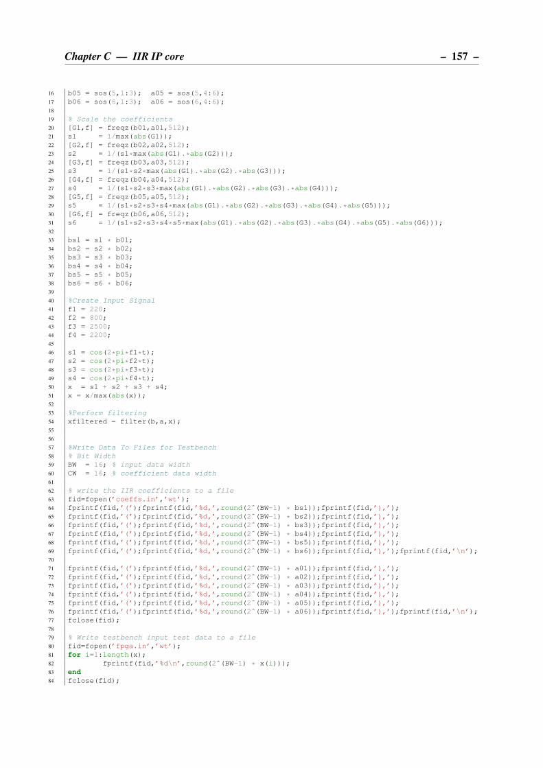
Chapter C — IIR IP core – 157 –
16 b05 = sos(5,1:3); a05 = sos(5,4:6);
17 b06 = sos(6,1:3); a06 = sos(6,4:6);
18
19 % Scale the coefficients
20 [G1,f] = freqz(b01,a01,512);
21 s1 = 1/max(abs(G1));
22 [G2,f] = freqz(b02,a02,512);
23 s2 = 1/(s1*max(abs(G1).*abs(G2)));
24 [G3,f] = freqz(b03,a03,512);
25 s3 = 1/(s1*s2*max(abs(G1).*abs(G2).*abs(G3)));
26 [G4,f] = freqz(b04,a04,512);
27 s4 = 1/(s1*s2*s3*max(abs(G1).*abs(G2).*abs(G3).*abs(G4)));
28 [G5,f] = freqz(b05,a05,512);
29 s5 = 1/(s1*s2*s3*s4*max(abs(G1).*abs(G2).*abs(G3).*abs(G4).*abs(G5)));
30 [G6,f] = freqz(b06,a06,512);
31 s6 = 1/(s1*s2*s3*s4*s5*max(abs(G1).*abs(G2).*abs(G3).*abs(G4).*abs(G5).*abs(G6)));
32
33 bs1 = s1 * b01;
34 bs2 = s2 * b02;
35 bs3 = s3 * b03;
36 bs4 = s4 * b04;
37 bs5 = s5 * b05;
38 bs6 = s6 * b06;
39
40 %Create Input Signal
41 f1 = 220;
42 f2 = 800;
43 f3 = 2500;
44 f4 = 2200;
45
46 s1 = cos(2*pi*f1*t);
47 s2 = cos(2*pi*f2*t);
48 s3 = cos(2*pi*f3*t);
49 s4 = cos(2*pi*f4*t);
50 x = s1 + s2 + s3 + s4;
51 x = x/max(abs(x));
52
53 %Perform filtering
54 xfiltered = filter(b,a,x);
55
56
57 %Write Data To Files for Testbench
58 % Bit Width
59 BW = 16; % input data width
60 CW = 16; % coefficient data width
61
62 % write the IIR coefficients to a file
63 fid=fopen(’coeffs.in’,’wt’);
64 fprintf(fid,’(’);fprintf(fid,’%d,’,round(2ˆ(BW-1) * bs1));fprintf(fid,’),’);
65 fprintf(fid,’(’);fprintf(fid,’%d,’,round(2ˆ(BW-1) * bs2));fprintf(fid,’),’);
66 fprintf(fid,’(’);fprintf(fid,’%d,’,round(2ˆ(BW-1) * bs3));fprintf(fid,’),’);
67 fprintf(fid,’(’);fprintf(fid,’%d,’,round(2ˆ(BW-1) * bs4));fprintf(fid,’),’);
68 fprintf(fid,’(’);fprintf(fid,’%d,’,round(2ˆ(BW-1) * bs5));fprintf(fid,’),’);
69 fprintf(fid,’(’);fprintf(fid,’%d,’,round(2ˆ(BW-1) * bs6));fprintf(fid,’),’);fprintf(fid,’\n’);
70
71 fprintf(fid,’(’);fprintf(fid,’%d,’,round(2ˆ(BW-1) * a01));fprintf(fid,’),’);
72 fprintf(fid,’(’);fprintf(fid,’%d,’,round(2ˆ(BW-1) * a02));fprintf(fid,’),’);
73 fprintf(fid,’(’);fprintf(fid,’%d,’,round(2ˆ(BW-1) * a03));fprintf(fid,’),’);
74 fprintf(fid,’(’);fprintf(fid,’%d,’,round(2ˆ(BW-1) * a04));fprintf(fid,’),’);
75 fprintf(fid,’(’);fprintf(fid,’%d,’,round(2ˆ(BW-1) * a05));fprintf(fid,’),’);
76 fprintf(fid,’(’);fprintf(fid,’%d,’,round(2ˆ(BW-1) * a06));fprintf(fid,’),’);fprintf(fid,’\n’);
77 fclose(fid);
78
79 % Write testbench input test data to a file
80 fid=fopen(’fpga.in’,’wt’);
81 for i=1:length(x);
82 fprintf(fid,’%d\n’,round(2ˆ(BW-1) * x(i)));
83 end
84 fclose(fid);

– 158 – Chapter C — IIR IP core
85
86 % Write MATLAB IIR filter model data to a file
87 fid=fopen(’matlab.out’,’wt’);
88 for i=1:length(x);
89 fprintf(fid,’%d\n’,round(2ˆ(CW-1) * xfiltered(i)));
90 end
91 fclose(fid);
92
93 % Plot FIlter frequency Response
94 [h,f] = freqz(b,a,1024,Fs);
95
96 subplot(2,2,2);
97 plot(f,20*log10(abs(h)),’k’)
98 title(’IIR filter frequency Response’);
99 xlabel(’Frequency ($Hz$)’);
100 ylabel(’Magnitude ($dB$)’);
101 xlim([0,5000]);
102 grid on;
C.3 PLOTTING THE RESULTS IN MATLAB
1 % ----------------------------------------------------------------------
2 % This plots FPGA and MATLAB results, it can be padded to the previous
3 % script for better plot graphical disply
4 % ----------------------------------------------------------------------
5 NFFT = 1024;
6 Ts = 1/Fs; % sampling interval
7 f = Fs*(-NFFT/2:NFFT/2-1)/NFFT; % frequency
8
9 fid = fopen(’fpga.in’);
10 fpgain = textscan(fid,’%f’,’Delimiter’,’\n’);
11 fclose(fid);
12
13 fid = fopen(’fpga.out’);
14 fpgaout = textscan(fid,’%f’,’Delimiter’,’\n’);
15 fclose(fid);
16
17 fid = fopen(’matlab.out’);
18 matlabout = textscan(fid,’%f’,’Delimiter’,’\n’);
19 fclose(fid);
20
21 % normalized FFT of signals
22 f1 = fftshift(fft(fpgain1,NFFT));
23 F1 = abs(f1)/(N);
24 f2 = fftshift(fft(matlabout1,NFFT));
25 F2 = abs(f2)/(N);
26 f3 = fftshift(fft(fpgaout1,NFFT));
27 F3 = abs(f3)/(N);
28
29 % FFT for IIR Testebech input signal
30 subplot(2,2,1);
31 plot(f,F1,’k’);
32 title(’Magnitude Spectrum of Input Signal’);
33 xlabel(’Frequency ($Hz$)’);
34 ylabel(’Magnitude’);
35 xlim([-5000,5000]);
36 grid on;
37
38 % FFT for MATLAB FIR output
39 subplot(2,2,3);
40 plot(f/1e3,F2,’k’);
41 title(’Magnitude Spectrum of Matlab IIR filter output’);
42 xlabel(’Frequency ($kHz$)’);
43 ylabel(’Magnitude’);
44 xlim([-5,5]);
45 grid on;
46
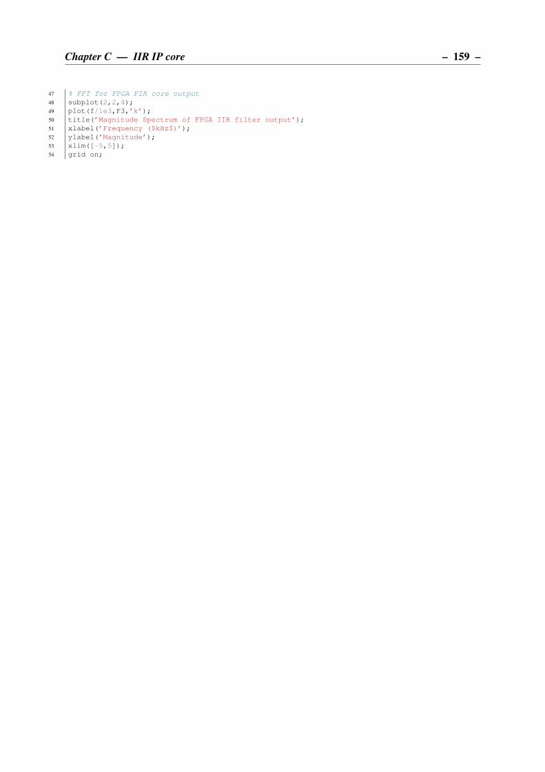
Chapter C — IIR IP core – 159 –
47 % FFT for FPGA FIR core output
48 subplot(2,2,4);
49 plot(f/1e3,F3,’k’);
50 title(’Magnitude Spectrum of FPGA IIR filter output’);
51 xlabel(’Frequency ($kHz$)’);
52 ylabel(’Magnitude’);
53 xlim([-5,5]);
54 grid on;

APPENDIX D
FFT/IFFT IP CORE
D.1 INSTANTIATION OF THE FFT/IFFT CORE
1 Library FFT_IFFT_Lib;
2 Use FFT_IFFT_Lib.fftcomponents.all;
3
4 -- r22sdf_fft_ifft_core_inst: This module implements a complex
5 -- N-point Radix 2ˆ2 single-path delay feedback
6 -- pipelined FFT or IFFT core with configurable
7 -- Input bit widths where N is powers of 2.
8 -- i.e. 8, 16, 32, 64, 128, 256, 512, 1024,
9 -- 2048, 4096. The input samples are in natural
10 -- order and ouput samples are in bit reversed order.
11 r22sdf_fft_ifft_core_inst : r22sdf_fft_ifft_core
12 generic map(
13 N => N, -- FFT Length
14 DIN_WIDTH => DIN_WIDTH, -- input data width
15 DOUT_WIDTH => DOUT_WIDTH,-- output data width
16 TF_W => TF_W, -- twiddle factor data width. default=16
17 MODE => ’0’ -- core select, ’0’=FFT,’1’=IFFT
18 )
19 port map(
20 clk => clk, -- system clock input
21 rst => rst, -- system reset input
22 en => en, -- clock enable input
23 XSr => XSr, -- real-part input sample
24 XSi => XSi, -- imaginary-part input sample
25 vld => vld, -- valid output result
26 done => done, -- fft process complete
27 XKr => XKr, -- real-part output sample
28 XKi => XKi -- imaginary-part output sample
29 );
D.2 GENERATING TESTBENCH DATA FILES IN MATLAB
1 % ----------------------------------------------------------------------
2 % This creates a rectungal pulse which is used as the input test data to
3 % 1024-point FFT core.
4 % ----------------------------------------------------------------------
5 bit_width = 16; % data width
6 N = 1024; % FFT length
7 A = 2ˆ(bit_width - 1); % amplitute
8 Fs = 50e6; % sampling frequency in KHz
9 t = -Fs/2:Fs/N:Fs/2-Fs/N;
10
11 %makes the actual square pulse
160
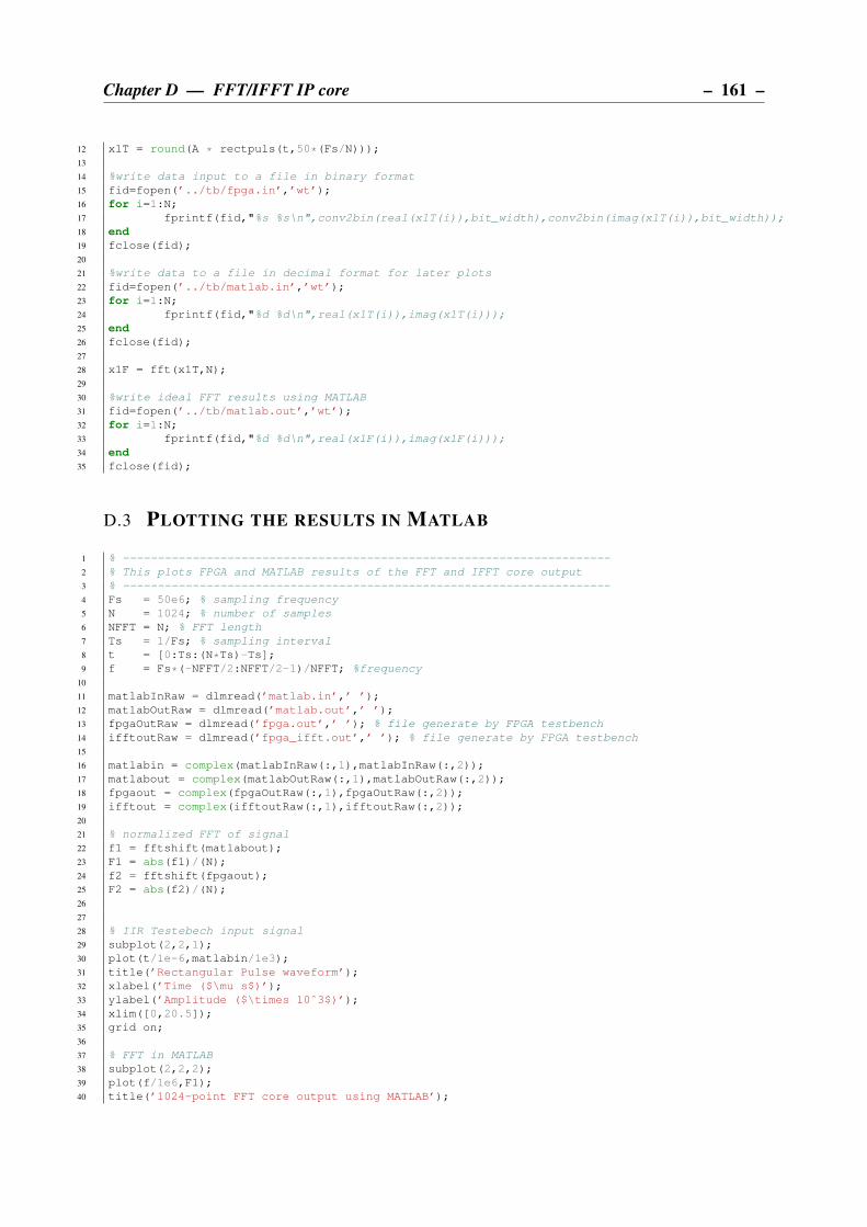
Chapter D — FFT/IFFT IP core – 161 –
12 x1T = round(A * rectpuls(t,50*(Fs/N)));
13
14 %write data input to a file in binary format
15 fid=fopen(’../tb/fpga.in’,’wt’);
16 for i=1:N;
17 fprintf(fid,"%s %s\n",conv2bin(real(x1T(i)),bit_width),conv2bin(imag(x1T(i)),bit_width));
18 end
19 fclose(fid);
20
21 %write data to a file in decimal format for later plots
22 fid=fopen(’../tb/matlab.in’,’wt’);
23 for i=1:N;
24 fprintf(fid,"%d %d\n",real(x1T(i)),imag(x1T(i)));
25 end
26 fclose(fid);
27
28 x1F = fft(x1T,N);
29
30 %write ideal FFT results using MATLAB
31 fid=fopen(’../tb/matlab.out’,’wt’);
32 for i=1:N;
33 fprintf(fid,"%d %d\n",real(x1F(i)),imag(x1F(i)));
34 end
35 fclose(fid);
D.3 PLOTTING THE RESULTS IN MATLAB
1 % ----------------------------------------------------------------------
2 % This plots FPGA and MATLAB results of the FFT and IFFT core output
3 % ----------------------------------------------------------------------
4 Fs = 50e6; % sampling frequency
5 N = 1024; % number of samples
6 NFFT = N; % FFT length
7 Ts = 1/Fs; % sampling interval
8 t = [0:Ts:(N*Ts)-Ts];
9 f = Fs*(-NFFT/2:NFFT/2-1)/NFFT; %frequency
10
11 matlabInRaw = dlmread(’matlab.in’,’ ’);
12 matlabOutRaw = dlmread(’matlab.out’,’ ’);
13 fpgaOutRaw = dlmread(’fpga.out’,’ ’); % file generate by FPGA testbench
14 ifftoutRaw = dlmread(’fpga_ifft.out’,’ ’); % file generate by FPGA testbench
15
16 matlabin = complex(matlabInRaw(:,1),matlabInRaw(:,2));
17 matlabout = complex(matlabOutRaw(:,1),matlabOutRaw(:,2));
18 fpgaout = complex(fpgaOutRaw(:,1),fpgaOutRaw(:,2));
19 ifftout = complex(ifftoutRaw(:,1),ifftoutRaw(:,2));
20
21 % normalized FFT of signal
22 f1 = fftshift(matlabout);
23 F1 = abs(f1)/(N);
24 f2 = fftshift(fpgaout);
25 F2 = abs(f2)/(N);
26
27
28 % IIR Testebech input signal
29 subplot(2,2,1);
30 plot(t/1e-6,matlabin/1e3);
31 title(’Rectangular Pulse waveform’);
32 xlabel(’Time ($\mu s$)’);
33 ylabel(’Amplitude ($\times 10ˆ3$)’);
34 xlim([0,20.5]);
35 grid on;
36
37 % FFT in MATLAB
38 subplot(2,2,2);
39 plot(f/1e6,F1);
40 title(’1024-point FFT core output using MATLAB’);
– 162 – Chapter D — FFT/IFFT IP core
41 xlabel(’Frequency ($MHz$)’);
42 ylabel(’Magnitude1’);
43 xlim([-25,25]);
44 grid on;
45
46 % FFT in FPGA
47 subplot(2,2,3);
48 plot(f/1e6,F2);
49 title(’1024-point FFT core output using FPGA’);
50 xlabel(’Frequency ($MHz$)’);
51 ylabel(’Magnitude’);
52 xlim([-25,25]);
53 grid on;
54
55 % IFFT in MATLAB
56 subplot(2,2,4);
57 plot(t/1e-6,abs(ifftout));
58 title(’1024-point IFFT core output using FPGA’);
59 xlabel(’Time ($\mu s$)’);
60 ylabel(’Amplitude’);
61 xlim([0,20.5]);
62 grid on;
D.3.1 Decimal to 2’s complement binary Conversion
1 % ----------------------------------------------------------------------
2 % Converts decimal to 2’complement binary
3 % ----------------------------------------------------------------------
4 function bin=conv2bin(num,Nbits);
5 % num : integer value to be converted to binanary
6 % Nbits: number of the binary bits in the output string
7
8 if(Nbits <= 8)
9 bin = dec2bin(typecast(int8(num),’uint8’));
10 elseif(Nbits <= 16)
11 bin = dec2bin(typecast(int16(num),’uint16’));
12 elseif(Nbits <= 32)
13 bin = dec2bin(typecast(int32(num),’uint32’));
14 elseif(Nbits <= 64)
15 bin = dec2bin(typecast(int64(num),’uint64’));
16 end
17 if(length(bin) < Nbits)
18 zero_count = Nbits - length(bin);
19 for i = 1:zero_count
20 bin = strcat(’0’,bin);
21 end
22 elseif(length(bin) > Nbits)
23 bin = substr(bin,length(bin)-Nbits + 1,Nbits);
24 end
D.4 GENERATING N-BIT TWIDDLE FACTORS HDL ROM
1 function r22sdf_twiddle_rom_gen(N,tf_bit_width);
2 % ----------------------------------------------------------------------------------------
3 % This generates DIF R2ˆ2-SDF FFT ROM of twiddle factors in 2’s complement number format
4 % ----------------------------------------------------------------------------------------
5 % [hd] = r22sdf_twiddle_rom_gen(N,tf_bit_width)
6 % N
7 % tf_bit_width = Bit width of twiddle factors
8 % ----------------------------------------------------------------------------------------
9 %
10 % at kth stage, k = 0,1,...ceil(log(N)/log(4))-2
11 % a[i] = eˆ(j*2*pi*p/N) = cos(2*pi*p/N) + jsin(2*pi*p/N)
12 % i = 0,1,2,...,(N/2ˆ2k-1)
Chapter D — FFT/IFFT IP core – 163 –
13 % m = N/2ˆ(2+2k)
14 % p = 0
15 % = 2 * 2ˆ((2*k)+1) * (i m) [ m i < 2*m ]
16 % = 2ˆ(k*2) * (i 2*m) [ 2*m i < 3*m ]
17 % = 3 * 2ˆ(2*k) * (i 3*m) [ 3*m i < 4*m ]
18 %
19 % ----------------------------------------------------------------------------------------
20
21 % compute the number of stages
22 stages_count = ceil(log(N)/log(4))-1;
23 for k = 0:stages_count-1;
24
25 % calculate rom depth for kth stage
26 rom_depth = N/(2ˆ(2*k));
27 % compute width of a rom height address
28 addr = log2(rom_depth);
29
30 % create vhdl file for kth fft stage
31 file_name = sprintf("data/fft%d_tf_rom_s%d.vhd",N,k);
32 fid=fopen(file_name,’wt’);
33 fprintf(fid,"--************************************************\n");
34 fprintf(fid,"--* Company: University of Cape Town\n");
35 fprintf(fid,"--* Engineer: Lekhobola Joachim Tsoeunyane\n");
36 fprintf(fid,"--***************************************************\n");
37 fprintf(fid,"--* Create Date: %s \n",datestr(now));
38 fprintf(fid,"--* Design Name: Pipelined R2ˆ2 DIF-SDF FFT \n");
39 fprintf(fid,"--* Module Name: fft%d_tf_rom_s%d.vhd\n",N,k);
40 fprintf(fid,"--* Project Name: RHINO SDR Processing Blocks\n");
41 fprintf(fid,"--* Target Devices: Xilinx - SPARTAN-6 \n");
42 fprintf(fid,"--****************************************************\n");
43 fprintf(fid,"--* Dependencies: none
44 \n");
45 fprintf(fid,"--*******************************************************46 ***********\n");
47 fprintf(fid,"LIBRARY IEEE;\n");
48 fprintf(fid,"USE IEEE.STD_LOGIC_1164.ALL;\n");
49 fprintf(fid,"USE IEEE.STD_LOGIC_UNSIGNED.ALL;\n");
50 fprintf(fid,"--********************************************************51 ***********\n");
52 fprintf(fid,"--* This module implements the stage-%d of twiddle factor
53 ROM for a %d-point \n",k,N);
54 fprintf(fid,"--* pipelined R2ˆ2 DIF-SDF FFT. Each value is a complex
55 numberimaginary,complex \n");
56 fprintf(fid,"--* ****************************************************57 ************\n");
58 fprintf(fid,"--* params:\n");
59 fprintf(fid,"--* addr_w - rom address bit width \n");
60 fprintf(fid,"--* data_w - output data bit width \n");
61 fprintf(fid,"--* ports:\n");
62 fprintf(fid,"--* [in] addr - Twidde factor ROM address to read\n");
63 fprintf(fid,"--* out] doutr - Twiddle factor read from rom addr - real value\n");
64 fprintf(fid,"--* [out] douti - Twidder factor read from rom addr - imaginary value\n");
65 fprintf(fid,"--*******************************************************************\n");
66 fprintf(fid,"--* Notes: Do not modify this file as it is auto-generated using matlab
67 script \n");
68 fprintf(fid,"--*******************************************************************\n");
69 fprintf(fid,"entity fft%d_tf_rom_s%d is\n",N,k);
70 fprintf(fid," generic(\n");
71 fprintf(fid," addr_w : natural := %d;\n",addr);
72 fprintf(fid," data_w : natural := %d\n",tf_bit_width);
73 fprintf(fid," );\n");
74 fprintf(fid," port (\n");
75 fprintf(fid," addr : in std_logic_vector (addr_w - 1 downto 0);\n");
76 fprintf(fid," doutr : out std_logic_vector (data_w - 1 downto 0);\n");
77 fprintf(fid," douti : out std_logic_vector(data_w - 1 downto 0)\n");
78 fprintf(fid," );\n");
79 fprintf(fid,"end fft%d_tf_rom_s%d;\n\n",N,k);
80
81 fprintf(fid,"architecture Behavioral of fft%d_tf_rom_s%d is\n",N,k);
– 164 – Chapter D — FFT/IFFT IP core
82 fprintf(fid," type complex is array(0 to 1) of std_logic_vector(data_w - 1 downto 0);\n");
83 fprintf(fid," type rom_type is array(0 to (2 ** addr_w) - 1) of complex;\n\n");
84
85 fprintf(fid," constant rom : rom_type := (\n");
86
87
88 % starting index for twiddle rom
89 s = rom_depth / 4;
90
91 printf("stage %d, factors = %d \n", k, rom_depth);
92 for i = 0:rom_depth-1;
93 % compute twiddle factor index
94 m = N/2ˆ(2+(2*k));
95 if (s < m)
96 p = 0;
97 elseif(s < (2*m))
98 p = 2ˆ(2*k+1)*(s-m);
99 elseif(s < (3*m))
100 p = 2ˆ(2*k)*(s-(2*m));
101 elseif(s < (4*m))
102 p = (3*2ˆ(2*k))*(s-(3*m));
103 end
104
105 s = s+1;
106 if(s == rom_depth)
107 s = 0;
108 end
109
110 % find a twiddle factor
111 tf = exp(-1j*2*pi*(p/N))
112 % real and imaginary of a twiddle factor
113 realval = real(tf);
114 imagval = imag(tf);
115 % round twiddle factor
116 rounded_real = realval*(2ˆ(tf_bit_width-2));
117 rounded_imag = imagval*(2ˆ(tf_bit_width-2));
118 % convert twiddle to binary
119 real_bin = conv2bin(rounded_real,tf_bit_width);
120 imag_bin = conv2bin(rounded_imag,tf_bit_width);
121 % write to file
122 if(i < rom_depth - 1)
123 fprintf(fid,"(\"%s\",\"%s\"),\n",real_bin,imag_bin);
124 else
125 fprintf(fid,"(\"%s\",\"%s\")\n",real_bin,imag_bin);
126 end
127
128 end
129 fprintf(fid,");\n");
130 fprintf(fid,"begin\n");
131 fprintf(fid," doutr <= std_logic_vector(rom(conv_integer(addr))(0));\n");
132 fprintf(fid," douti <= std_logic_vector(rom(conv_integer(addr))(1));\n");
133 fprintf(fid,"end Behavioral;\n");
134 fclose(fid);
135 end

APPENDIX E
DDC IP CORE
E.1 INSTANTIATION OF THE DDC CORE
1 Library FIR_Lib;
2 Use FIR_Lib.fir_pkg.all;
3
4 Library DDC_Lib;
5 Use DDC_Lib.ddccomponents.all;
6
7 -- DDC__inst: This implements a Digital Down Converter on the FPGA.
8 -- The cores mainly on other sub-blocks such as NCO,
9 -- digital mixer, CIC and compensation FIR filter.
10 ddc_inst : ddc
11 generic map(
12 DIN_WIDTH => DIN_WIDTH, -- input data width
13 DOUT_WIDTH => DOUT_WIDTH, -- output data width
14 -- NCO Configurations
15 PHASE_WIDTH => PHASE_WIDTH, -- NCO phase width
16 PHASE_DITHER_WIDTH => PHASE_DITHER_WIDTH, -- Phase dither width
17 -- CIC 1 configurations
18 SELECT_CIC1 => SELECT_CIC1, -- select CIC decimator 1
19 NUMBER_OF_STAGES1 => NUMBER_OF_STAGES1, -- number of stages
20 DIFFERENTIAL_DELAY1 => DIFFERENTIAL_DELAY1, --differential Dealy
21 SAMPLE_RATE_CHANGE1 => SAMPLE_RATE_CHANGE1, --decimation factor
22 -- Compensation FIR configuratons
23 SELECT_CFIR => SELECT_CFIR, -- use FIR filter
24 NUMBER_OF_TAPS => NUMBER_OF_TAPS, -- number of filter coefficients
25 FIR_LATENCY => FIR_LATENCY, -- FIR filter structure type
26 COEFF_WIDTH => COEFF_WIDTH, -- coefficient data width
27 COEFFS => COEFFS, -- array of quantized filter coefficients
28 -- CIC 2 configurations
29 SELECT_CIC2 => SELECT_CIC2, -- select CIC decimator 2
30 NUMBER_OF_STAGES2 => NUMBER_OF_STAGES2, -- number of stages
31 DIFFERENTIAL_DELAY2 => DIFFERENTIAL_DELAY2, -- differential delay
32 SAMPLE_RATE_CHANGE2 => SAMPLE_RATE_CHANGE2 -- decimation factor
33 )
34 port map(
35 clk => clk, -- system clock input
36 rst => rst, -- system reset input
37 en => en, -- clock enable input
38 din => din, -- input data sample
39 ftw => ftw, -- frequency tuning word
40 vld => vld, -- valid output result
41 iout => iout, -- real-part baseband output sample
42 qout => qout -- imaginary-part baseband output sample
43 );
165

– 166 – Chapter E — DDC IP core
E.2 GENERATING TESTBENCH DATA FILES IN MATLAB
1 %-----------------------------------------------------------------------
2 % This generates an FM signal as the input test factor to the DDC core
3 % testbench.
4 %-----------------------------------------------------------------------
5 N = 8192*4; % total # of samples
6 Fs = 122.88e6; % perform undersampling of FM signal
7 Ts = 1/Fs; % sampling interval
8 fc = 94.5e6; % carrier frequency
9
10 t = [0:Ts:(N*Ts)- Ts]; % time index for samples
11
12 % system impedance (ohms)
13 R = 50;
14
15 % FM modulate a test signal.
16 ModFreq = 15e3; % Modulating frequency
17 carrier = cos(2*pi*fc*t);
18
19
20 msg = awgn(sin(2*pi*ModFreq*t), 20, ’measured’); % compute vector
21
22 mi = 1; % Modulation Index
23 fmmsg = 2ˆ15 * cos(2*pi*fc*t + mi*msg);
24
25 % PLOTS
26 startplot = 1;
27 endplot = 1000;
28
29 NFFT = N; % FFT length
30 Ts = 1/Fs; % sampling interval
31 f = Fs*(-NFFT/2:NFFT/2-1)/NFFT; % frequency
32
33 figure(1);
34 subplot(2,2,1);
35 plot(t/1e-6, msg,’k’);
36 title(’Message Signal’);
37 xlabel(’Time ($\mu s$)’);
38 ylabel(’Amplitude’);
39 grid on;
40
41 % FFT for a baseband signal
42 f1 = fftshift(fft(msg,NFFT));
43 F1 = abs(f1)/(N);
44
45 subplot(2,2,2);
46 plot(f/1e3,F1,’k’);
47 title(’Magnitude Spectrum of a Message Signal’);
48 xlabel(’Frequency ($kHz$)’);
49 ylabel(’Magnitude’);
50 xlim([-50,50]);
51 grid on;
52
53 % FFT for a carrier signal
54 f2 = fftshift(fft(2ˆ15*carrier,NFFT));
55 F2 = abs(f2)/(N);
56
57 subplot(2,2,3);
58 plot(f/1e6,F2/1e4,’k’);
59 title(’Magnitude spectrum of a carrier’);
60 xlabel(’Frequency ($MHz$)’);
61 ylabel(’Magnitude ($\times 10ˆ4$)’);
62 xlim([-62,62]);
63 grid on;
64
65 % FFT for FM signal
66 f3 = fftshift(fft(fmmsg,NFFT));
67 F3 = abs(f3)/(N);

Chapter E — DDC IP core – 167 –
68
69 subplot(2,2,4);
70 plot(f/1e6,F3,’k’);
71 title(’Magnitude spectrum of FM Modulated signal’);
72 xlabel(’Frequency ($MHz$)’);
73 ylabel(’Magnitude’);
74 xlim([27,29]);
75 grid on;
76
77 %-----------------------------------------------------------------------
78 % Digital Down Conversion (DDC) SIMULATION BEFORE IMPLEMENTATION ON FPGA
79 %-----------------------------------------------------------------------
80
81 %
82 %-----------------------------------------------------------------------
83 %nco = ideal_dds(Fs,17.5e6,N); % digital local oscillator
84 %fLO = 2*Fs - fc;
85 fLO = Fs - fc;
86 LO = exp(-1*1j*2*pi*fLO*t);
87
88 % normalized FFT of signal
89 f4=(fftshift(fft(LO,N))/(N));
90
91 % power spectrum
92 F4 = 10*log10((abs(f4).ˆ2)/R*1000);
93
94 figure(2);
95 subplot(2,2,1);
96 plot(f,F4);
97 title(’spectrum of a Local Oscillator ( LO[n] )’);
98 xlabel(’Frequency [hertz]’);
99 ylabel(’Magnitude [dB]’);
100 xlim([-30e6,0]);
101
102 %
103 %-----------------------------------------------------------------------
104 mixer = fmmsg .* LO; % mix FM signal with LO
105
106 % normalized FFT of signal
107 f5=(fftshift(fft(mixer,N))/(N));
108
109 % power spectrum
110 F5 = 10*log10((abs(f5).ˆ2)/R*1000);
111
112 subplot(2,2,2);
113 plot(f,F5);
114 title(’Spectrum of a mixer signal ( b[n] )’);
115 xlabel(’Frequency [hertz]’);
116 ylabel(’Magnitude [dB]’);
117 xlim([-10e6,30e6]);
118
119 %
120 %-----------------------------------------------------------------------
121 Mcic = 1; % Differential delays in the filter.
122 Ncic = 10; % Filter sections
123 Rcic = 128; % Decimation factor
124
125 g = ones(1,Rcic*Mcic);
126 h = g;
127 for i=1:Ncic;
128 h = conv(h,g);
129 end;
130
131 cic_filtered = conv(mixer,g);
132 cic = cic_filtered([1:Rcic:length(cic_filtered)]);
133 cic = cic(1:round(length(mixer)/Rcic));
134
135 Fs = round(Fs/Rcic);
136 Ts = 1/Fs;
– 168 – Chapter E — DDC IP core
137 N = round(N/Rcic);
138 t = [0:Ts:(N*Ts)- Ts];
139
140 dF = Fs/N; % hertz
141 f = -Fs/2:dF:Fs/2-dF; % hertz
142
143 % normalized FFT of signal
144 f6=(fftshift(fft(cic,N))/(N));
145
146 % power spectrum
147 F6 = 10*log10((abs(f6).ˆ2)/R*1000);
148
149 subplot(2,2,3);
150 plot(f,F6);
151 title(’Spectrum of a CIC output ( c[n] )’);
152 xlabel(’Frequency [hertz]’);
153 ylabel(’Magnitude [dB]’);
154 xlim([-1.5e6,1.5e6]);
155
156
157 %
158 %-----------------------------------------------------------------------
159
160 Hfir= cfir(Rcic,Mcic,Ncic,95e3,122.88e6);
161
162 % filter the mixer spurs
163 pfir = filter(Hfir,1,cic);
164
165 % normalized FFT of signal
166 f7=(fftshift(fft(pfir,N))/(N));
167
168 % power spectrum
169 F7 = 10*log10((abs(f7).ˆ2)/R*1000);
170
171 subplot(2,2,4);
172 plot(f,F7);
173 title(’Spectrum of a filter output [I[n] and Q[n]’);
174 xlabel(’Frequency [hertz]’);
175 ylabel(’Magnitude [dB]’);
176 xlim([-1.5e6,1.5e6]);
177
178 % Write test data to a file
179 fid=fopen(’../../tb/coeffs.in’,’wt’);
180 fprintf(fid,"%d,",round(Hfir*2ˆ15));
181 fclose(fid);
182
183 %
184 %-----------------------------------------------------------------------
185 Mcic = 1; % Differential delays in the filter.
186 Ncic = 1; % Filter sections
187 Rcic = 2; % Decimation factor
188
189 g = ones(1,Rcic*Mcic);
190 h = g;
191 for i=1:Ncic;
192 h = conv(h,g);
193 end;
194
195 cic1 = pfir;
196 cic_filtered = conv(cic1,g);
197 cic = cic_filtered([1:Rcic:length(cic_filtered)]);
198 cic = cic(1:round(length(cic1)/Rcic));
199
200 Fs = round(Fs/Rcic);
201 Ts = 1/Fs;
202 N = round(N/Rcic);
203 t = [0:Ts:(N*Ts)- Ts];
204
205 dF = Fs/N; % hertz

Chapter E — DDC IP core – 169 –
206 f = -Fs/2:dF:Fs/2-dF; % hertz
207
208 %-----------------------------------------------------------------------
209 %
210 %-----------------------------------------------------------------------
211
212 % Initialize the variables. %
213
214 phase = zeros(1,length(cic));
215 freq = zeros(1,length(cic)-1);
216
217 phase = atan2(imag(cic),real(cic));
218 freq = phase(1)
219 freq = diff(phase)./diff(t);
220
221 freq = -1 .* freq;
222
223 % amplify the output
224 %freq = (1/max(freq(50:length(freq)))) * freq;
225
226 %-------------------------------------------------------------------------%
227 figure(3)
228 subplot(2,2,1)
229 plot(t(1:length(t)-1),freq);
230 title(’FM Demodulated Signal’);
231 xlabel(’Time (seconds)’);
232 ylabel(’Amplitude’);
233 %ylim([-1,1]);
234
235 % normalized FFT of signal
236 f8=(fftshift(fft(freq,N))/(N));
237
238 % power spectrum
239 F8 = 10*log10((abs(f8).ˆ2)/R*1000);
240
241 subplot(2,2,2)
242 plot(f,F8);
243 title(’Spectrum of a Demodulated Signals’);
244 xlabel(’Frequency [hertz]’);
245 ylabel(’Magnitude [dB]’);
246 xlim([-20e3,20e3]);
E.3 GENERATE COEFFICIENTS FOR A COMPENSATION FILTER
1 function [h]= cfir(R,M,N);
2 %%%%%% CIC filter parameters %%%%%%
3 %R,M,N
4 %h = filter response
5 B = 16; %% Coeffi. Bit-width
6 Fs = 122.88e6;%% (High) Sampling freq in Hz before decimation
7 Fc = 80e3; %% Pass band edge in Hz
8
9 L = 20; %% Filter order; must be even
10 Fo = R*Fc/Fs; %% Normalized Cutoff freq; 0<Fo<=0.5/M;
11
12 p = 2e3; %% Granularity
13 s = 0.25/p; %% Step size
14 fp = [0:s:Fo]; %% Pass band frequency samples
15 fs = (Fo+s):s:0.5; %% Stop band frequency samples
16 f = [fp fs]*2; %% Normalized frequency samples; 0<=f<=1
17 Mp = ones(1,length(fp)); %% Pass band response; Mp(1)=1
18 Mp(2:end) = abs( M*R*sin(pi*fp(2:end)/R)./sin(pi*M*fp(2:end))).ˆN;
19 Mf = [Mp zeros(1,length(fs))];
20 f(end) = 1;
21 h = fir2(L,f,Mf); %% Filter length L+1

– 170 – Chapter E — DDC IP core
E.4 PLOTTING THE RESULTS IN MATLAB
1 %-----------------------------------------------------------------------
2 % Plotting the results of the DDC core output
3 %-----------------------------------------------------------------------
4 N = 8192*4; % total # of samples
5 Fs = 122.88e6; % perform undersampling of FM signal
6 Ts = 1/Fs; % sampling interval
7 f = Fs*(-NFFT/2:NFFT/2-1)/NFFT; % frequency
8
9 % Numerially-Controlled Oscillator
10 ncoOutRaw = dlmread(’nco.out’,’ ’);
11 ncoOut = complex(ncoOutRaw(:,1),ncoOutRaw(:,2));
12
13 % normalized FFT of signal
14 f4 = fftshift(fft(ncoOut,NFFT));
15 F4 = abs(f4)/(N);
16
17 figure(2);
18 subplot(2,2,1);
19 plot(f/1e6,F4,’k’);
20 title(’Magnitude spectrum of NCO’);
21 xlabel(’Frequency ($MHz$)’);
22 ylabel(’Magnitude’);
23 xlim([0,61.44]);
24 grid on;
25
26 % Mixer Stage of DDC
27
28 mixerOutRaw = dlmread(’mixer.out’,’ ’);
29 mixerOut = complex(mixerOutRaw(:,1),mixerOutRaw(:,2));
30
31 % normalized FFT of signal
32 f5 = fftshift(fft(mixerOut,NFFT));
33 F5 = abs(f5)/(N);
34
35 subplot(2,2,2);
36 plot(f/1e6,F5,’k’);
37 title(’Magnitude spectrum of a Mixer’);
38 xlabel(’Frequency ($MHz$)’);
39 ylabel(’Magnitude’);
40 xlim([-10,61.44]);
41 grid on;
42
43 %CIC Stage 1
44 NFFT = round(N/153);
45 Ts = 1/(Fs/153);
46 Fs = 1/Ts; % sampling interval
47 f = Fs*(-NFFT/2:NFFT/2-1)/NFFT;
48
49 cic1OutRaw = dlmread(’cic1.out’,’ ’);
50 cic1Out = complex(cic1OutRaw(:,1),cic1OutRaw(:,2));
51
52 % normalized FFT of signal
53 f6 = fftshift(fft(cic1Out,NFFT));
54 F6 = abs(f6)/(N);
55
56 subplot(2,2,3);
57 plot(f/1e3,F6/1e4,’k’);
58 title(’Magnitude spectrum of CIC-1’);
59 xlabel(’Frequency ($kHz$)’);
60 ylabel(’Magnitude ($\times 10ˆ4$)’);
61 %xlim([-400,400]);
62 grid on;
63
64 %Compensation FIR Stage 1
65 cfirOutRaw = dlmread(’cfir.out’,’ ’);
66 cfirOut = complex(cfirOutRaw(:,1),cfirOutRaw(:,2));
67

Chapter E — DDC IP core – 171 –
68 % normalized FFT of signal
69 f7 = fftshift(fft(cfirOut,NFFT));
70 F7 = abs(f7)/(N);
71
72 subplot(2,2,4);
73 plot(f/1e3,F7/1e4,’k’);
74 title(’Magnitude spectrum of a C-FIR filter’);
75 xlabel(’Frequency ($kHz$)’);
76 ylabel(’Magnitude ($\times 10ˆ4$)’);
77 %xlim([-400,400]);
78 grid on;
79
80 % CIC Stage 2
81 NFFT = round(N/153/2);
82 Ts = 1/(Fs/2);
83 Fs = 1/Ts;
84 f = Fs*(-NFFT/2:NFFT/2-1)/NFFT;
85
86 cic2OutRaw = dlmread(’cic2.out’,’ ’);
87 cic2Out = complex(cic2OutRaw(:,1),cic2OutRaw(:,2));
88
89 % normalized FFT of signal
90 f8 = fftshift(fft(cic2Out,NFFT));
91 F8 = abs(f8)/(N);
92
93 figure(3);
94 subplot(2,2,1);
95 plot(f/1e3,F8/1e4,’k’);
96 title(’Magnitude spectrum of CIC-2’);
97 xlabel(’Frequency ($kHz$)’);
98 ylabel(’Magnitude ($\times 10ˆ4$)’);
99 xlim([-200,200]);
100 grid on;
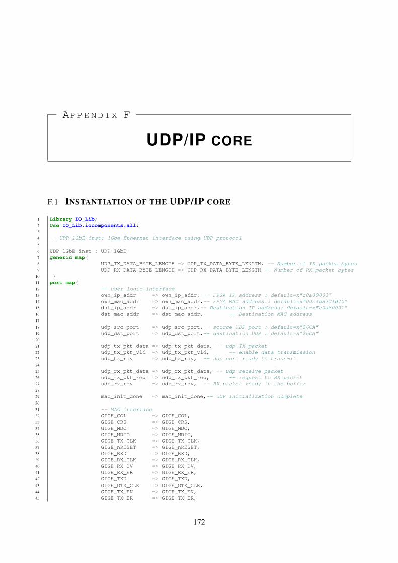
APPENDIX F
UDP/IP CORE
F.1 INSTANTIATION OF THE UDP/IP CORE
1 Library IO_Lib;
2 Use IO_Lib.iocomponents.all;
3
4 -- UDP_1GbE_inst: 1Gbe Ethernet interface using UDP protocol
5
6 UDP_1GbE_inst : UDP_1GbE
7 generic map(
8 UDP_TX_DATA_BYTE_LENGTH => UDP_TX_DATA_BYTE_LENGTH, -- Number of TX packet bytes
9 UDP_RX_DATA_BYTE_LENGTH => UDP_RX_DATA_BYTE_LENGTH -- Number of RX packet bytes
10 )
11 port map(
12 -- user logic interface
13 own_ip_addr => own_ip_addr, -- FPGA IP address : default=x"c0a80003"
14 own_mac_addr => own_mac_addr,-- FPGA MAC address : default=x"0024ba7d1d70"
15 dst_ip_addr => dst_ip_addr,-- Destination IP address: default=x"c0a80001"
16 dst_mac_addr => dst_mac_addr, -- Destination MAC address
17
18 udp_src_port => udp_src_port,-- source UDP port : default=x"26CA"
19 udp_dst_port => udp_dst_port,-- destination UDP : default=x"26CA"
20
21 udp_tx_pkt_data => udp_tx_pkt_data, -- udp TX packet
22 udp_tx_pkt_vld => udp_tx_pkt_vld, -- enable data transmission
23 udp_tx_rdy => udp_tx_rdy, -- udp core ready to transmit
24
25 udp_rx_pkt_data => udp_rx_pkt_data, -- udp receive packet
26 udp_rx_pkt_req => udp_rx_pkt_req, -- request to RX packet
27 udp_rx_rdy => udp_rx_rdy, -- RX packet ready in the buffer
28
29 mac_init_done => mac_init_done,-- UDP initialization complete
30
31 -- MAC interface
32 GIGE_COL => GIGE_COL,
33 GIGE_CRS => GIGE_CRS,
34 GIGE_MDC => GIGE_MDC,
35 GIGE_MDIO => GIGE_MDIO,
36 GIGE_TX_CLK => GIGE_TX_CLK,
37 GIGE_nRESET => GIGE_nRESET,
38 GIGE_RXD => GIGE_RXD,
39 GIGE_RX_CLK => GIGE_RX_CLK,
40 GIGE_RX_DV => GIGE_RX_DV,
41 GIGE_RX_ER => GIGE_RX_ER,
42 GIGE_TXD => GIGE_TXD,
43 GIGE_GTX_CLK => GIGE_GTX_CLK,
44 GIGE_TX_EN => GIGE_TX_EN,
45 GIGE_TX_ER => GIGE_TX_ER,
172

Chapter F — UDP/IP core – 173 –
46
47 -- system control
48 clk_125mhz => clk_125mhz,
49 clk_100mhz => clk_100mhz,
50 sys_rst_i => sys_rst_i,
51 sysclk_locked => sysclk_locked
52 );

APPENDIX G
ADC/DAC CORE
G.1 INSTANTIATION OF THE ADC/DAC CORE FOR INTERFACING FMC150
1 Library IO_Lib;
2 Use IO_Lib.iocomponents.all;
3
4 -- fmc150_if_inst: 1Gbe Ethernet interface using UDP protocol
5
6 fmc150_if_inst : fmc150_if
7 port map(
8
9 --RHINO Resources
10 sysrst => sysrst,
11 clk_100MHz => clk_100MHz,
12 mmcm_locked => mmcm_locked,
13
14 clk_61_44MHz => clk_61_44MHz,
15 clk_122_88MHz => clk_122_88MHz,
16 mmcm_adac_locked => mmcm_adac_locked,
17
18 -------------- user design interface -----------------------
19 -- ADC
20 adc_cha_dout => adc_cha_dout,
21 adc_chb_dout => adc_chb_dout,
22
23 -- DAC
24 dac_chc_din => dac_chc_din,
25 dac_chd_din => dac_chd_din,
26
27 calibration_ok => calibration_ok,
28
29 -------------- physical external interface -----------------
30
31 --Clock/Data connection to ADC on FMC150 (ADS62P49)
32 clk_ab_p => clk_ab_p,
33 clk_ab_n => clk_ab_n,
34 cha_p => cha_p,
35 cha_n => cha_n,
36 chb_p => chb_p,
37 chb_n => chb_n,
38
39 --Clock/Data connection to DAC on FMC150 (DAC3283)
40 dac_dclk_p => dac_dclk_p,
41 dac_dclk_n => dac_dclk_n,
42 dac_data_p => dac_data_p,
43 dac_data_n => dac_data_n,
44 dac_frame_p => dac_frame_p,
45 dac_frame_n => dac_frame_n,
174
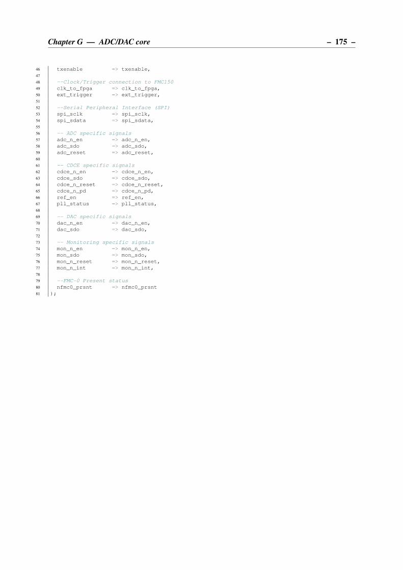
Chapter G — ADC/DAC core – 175 –
46 txenable => txenable,
47
48 --Clock/Trigger connection to FMC150
49 clk_to_fpga => clk_to_fpga,
50 ext_trigger => ext_trigger,
51
52 --Serial Peripheral Interface (SPI)
53 spi_sclk => spi_sclk,
54 spi_sdata => spi_sdata,
55
56 -- ADC specific signals
57 adc_n_en => adc_n_en,
58 adc_sdo => adc_sdo,
59 adc_reset => adc_reset,
60
61 -- CDCE specific signals
62 cdce_n_en => cdce_n_en,
63 cdce_sdo => cdce_sdo,
64 cdce_n_reset => cdce_n_reset,
65 cdce_n_pd => cdce_n_pd,
66 ref_en => ref_en,
67 pll_status => pll_status,
68
69 -- DAC specific signals
70 dac_n_en => dac_n_en,
71 dac_sdo => dac_sdo,
72
73 -- Monitoring specific signals
74 mon_n_en => mon_n_en,
75 mon_sdo => mon_sdo,
76 mon_n_reset => mon_n_reset,
77 mon_n_int => mon_n_int,
78
79 --FMC-0 Present status
80 nfmc0_prsnt => nfmc0_prsnt
81 );
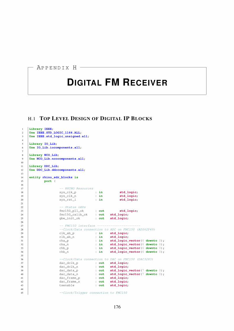
APPENDIX H
DIGITAL FM RECEIVER
H.1 TOP LEVEL DESIGN OF DIGITAL IP BLOCKS
1 Library IEEE;
2 Use IEEE.STD_LOGIC_1164.ALL;
3 Use IEEE.std_logic_unsigned.all;
4
5 Library IO_Lib;
6 Use IO_Lib.iocomponents.all;
7
8 Library NCO_Lib;
9 Use NCO_Lib.ncocomponents.all;
10
11 Library DDC_Lib;
12 Use DDC_Lib.ddccomponents.all;
13
14 entity rhino_sdr_blocks is
15 port (
16
17 -- RHINO Resources
18 sys_clk_p : in std_logic;
19 sys_clk_n : in std_logic;
20 sys_rst_i : in std_logic;
21
22 -- Status LEDs
23 fmc150_pll_ok : out std_logic;
24 fmc150_calib_ok : out std_logic;
25 gbe_init_ok : out std_logic;
26
27 -- FMC150 interface -----------------------
28 --Clock/Data connection to ADC on FMC150 (ADS62P49)
29 clk_ab_p : in std_logic;
30 clk_ab_n : in std_logic;
31 cha_p : in std_logic_vector(6 downto 0);
32 cha_n : in std_logic_vector(6 downto 0);
33 chb_p : in std_logic_vector(6 downto 0);
34 chb_n : in std_logic_vector(6 downto 0);
35
36 --Clock/Data connection to DAC on FMC150 (DAC3283)
37 dac_dclk_p : out std_logic;
38 dac_dclk_n : out std_logic;
39 dac_data_p : out std_logic_vector(7 downto 0);
40 dac_data_n : out std_logic_vector(7 downto 0);
41 dac_frame_p : out std_logic;
42 dac_frame_n : out std_logic;
43 txenable : out std_logic;
44
45 --Clock/Trigger connection to FMC150
176

Chapter H — Digital FM Receiver – 177 –
46 clk_to_fpga : in std_logic;
47 ext_trigger : in std_logic;
48
49 --Serial Peripheral Interface (SPI)
50 spi_sclk : out std_logic; -- Shared SPI clock line
51 spi_sdata : out std_logic; -- Shared SPI sata line
52
53 -- ADC specific signals
54 adc_n_en : out std_logic; -- SPI chip select
55 adc_sdo : in std_logic; -- SPI data out
56 adc_reset : out std_logic; -- SPI reset
57
58 -- CDCE specific signals
59 cdce_n_en : out std_logic; -- SPI chip select
60 cdce_sdo : in std_logic; -- SPI data out
61 cdce_n_reset : out std_logic;
62 cdce_n_pd : out std_logic;
63 ref_en : out std_logic;
64 pll_status : in std_logic;
65
66 -- DAC specific signals
67 dac_n_en : out std_logic; -- SPI chip select
68 dac_sdo : in std_logic; -- SPI data out
69
70 -- Monitoring specific signals
71 mon_n_en : out std_logic; -- SPI chip select
72 mon_sdo : in std_logic; -- SPI data out
73 mon_n_reset : out std_logic;
74 mon_n_int : in std_logic;
75
76 --FMC Present status
77 nfmc0_prsnt : in std_logic;
78
79 -- 1Gbps MAC interface
80
81 GIGE_COL : in std_logic;
82 GIGE_CRS : in std_logic;
83 GIGE_MDC : out std_logic;
84 GIGE_MDIO : inout std_logic;
85 GIGE_TX_CLK : in std_logic;
86 GIGE_nRESET : out std_logic;
87 GIGE_RXD : in std_logic_vector( 7 downto 0 );
88 GIGE_RX_CLK : in std_logic;
89 GIGE_RX_DV : in std_logic;
90 GIGE_RX_ER : in std_logic;
91 GIGE_TXD : out std_logic_vector( 7 downto 0 );
92 GIGE_GTX_CLK : out std_logic;
93 GIGE_TX_EN : out std_logic;
94 GIGE_TX_ER : out std_logic
95 );
96 end rhino_sdr_blocks;
97
98 architecture Behavioral of rhino_sdr_blocks is
99
100 --
101 component clk_manager is
102 port(
103 --External Control
104 SYS_CLK_P_i : in std_logic;
105 SYS_CLK_N_i : in std_logic;
106 SYS_RST_i : in std_logic;
107
108 clk_ab_p : in std_logic;
109 clk_ab_n : in std_logic;
110
111 -- Clock out ports
112 clk_125mhz : out std_logic;
113 clk_122_88mhz : out std_logic;
114 clk_100mhz : out std_logic;

– 178 – Chapter H — Digital FM Receiver
115 clk_61_44mhz : out std_logic;
116 clk_25mhz : out std_logic;
117
118 -- Status and control signals
119 RESET : out std_logic;
120 sysclk_locked : out std_logic;
121 adcclk_locked : out std_logic
122 );
123 end component clk_manager;
124
125 component adc_eth_bridge
126 generic(
127 MEM_DATA_BYTES : natural;
128 MEM_DEPTH : natural
129 );
130 port(
131 rst : in std_logic;
132 clk : in std_logic;
133 en : in std_logic;
134 rd_en : in std_logic;
135 vld : out std_logic;
136 new_pkt_rcvd : in std_logic;
137 din : in std_logic_vector(8 * MEM_DATA_BYTES - 1 downto 0);
138 dout : out std_logic_vector(8 * MEM_DATA_BYTES * MEM_DEPTH - 1 downto 0);
139 count : out std_logic_vector(6 downto 0)
140 );
141 end component;
142
143 -- Debugging Components and Signals
144 component icon
145 PORT (
146 CONTROL0 : INOUT STD_LOGIC_VECTOR(35 DOWNTO 0);
147 CONTROL1 : INOUT STD_LOGIC_VECTOR(35 DOWNTO 0);
148 CONTROL2 : INOUT STD_LOGIC_VECTOR(35 DOWNTO 0));
149
150 end component;
151
152 component ila0
153 PORT (
154 CONTROL : INOUT STD_LOGIC_VECTOR(35 DOWNTO 0);
155 CLK : IN STD_LOGIC;
156 DATA : IN STD_LOGIC_VECTOR(69 DOWNTO 0);
157 TRIG0 : IN STD_LOGIC_VECTOR(3 DOWNTO 0));
158
159 end component;
160
161 component ila1
162 PORT (
163 CONTROL : INOUT STD_LOGIC_VECTOR(35 DOWNTO 0);
164 CLK : IN STD_LOGIC;
165 DATA : IN STD_LOGIC_VECTOR(47 DOWNTO 0);
166 TRIG0 : IN STD_LOGIC_VECTOR(7 DOWNTO 0));
167
168 end component;
169
170 component vio
171 PORT (
172 CONTROL : INOUT STD_LOGIC_VECTOR(35 DOWNTO 0);
173 ASYNC_OUT : OUT STD_LOGIC_VECTOR(31 DOWNTO 0));
174
175 end component;
176
177
178 signal CONTROL0 : STD_LOGIC_VECTOR(35 DOWNTO 0);
179 signal CONTROL1 : STD_LOGIC_VECTOR(35 DOWNTO 0);
180 signal CONTROL2 : STD_LOGIC_VECTOR(35 DOWNTO 0);
181 signal ila_data0 : STD_LOGIC_VECTOR(69 DOWNTO 0);
182 signal ila_data1 : STD_LOGIC_VECTOR(47 DOWNTO 0);
183 signal trig0 : STD_LOGIC_VECTOR(3 DOWNTO 0);

Chapter H — Digital FM Receiver – 179 –
184 signal trig1 : STD_LOGIC_VECTOR(7 DOWNTO 0);
185 signal vio_data : STD_LOGIC_VECTOR(31 DOWNTO 0);
186
187 -- End
188
189
190 --
191
192 attribute S: string;
193 attribute keep : string;
194
195 -- FMC150 signals
196 attribute S of GIGE_RXD : signal is "TRUE";
197 attribute S of GIGE_RX_DV : signal is "TRUE";
198 attribute S of GIGE_RX_ER : signal is "TRUE";
199
200 constant UDP_TX_DATA_BYTE_LENGTH : integer := 64;
201 constant UDP_RX_DATA_BYTE_LENGTH : integer := 37;
202 constant TX_DELAY : integer := 10;
203
204 signal adc_cha_dout : std_logic_vector(13 downto 0);
205 signal adc_chb_dout : std_logic_vector(13 downto 0);
206
207 signal dac_chc_din : std_logic_vector(15 downto 0);
208 signal dac_chd_din : std_logic_vector(15 downto 0);
209
210 signal clk_100MHz : std_logic;
211 signal mmcm_locked : std_logic;
212 signal dac_fpga_clk : std_logic;
213
214 ------------------------- MAC signals -------------------------------------
215 signal udp_tx_pkt_data : std_logic_vector (8 * UDP_TX_DATA_BYTE_LENGTH - 1 downto 0);
216 signal udp_tx_pkt_vld : std_logic;
217 signal udp_tx_pkt_sent : std_logic;
218 signal udp_tx_pkt_vld_r : std_logic;
219 signal udp_tx_rdy : std_logic;
220
221 signal udp_rx_pkt_data : std_logic_vector(8 * UDP_RX_DATA_BYTE_LENGTH - 1 downto 0);
222 signal udp_rx_pkt_data_r: std_logic_vector(8 * UDP_RX_DATA_BYTE_LENGTH - 1 downto 0);
223 signal udp_rx_pkt_req : std_logic;
224 signal udp_rx_rdy : std_logic;
225 signal udp_rx_rdy_r : std_logic;
226
227 signal dst_mac_addr : std_logic_vector(47 downto 0);
228 signal tx_state : std_logic_vector(2 downto 0) := "000";
229 signal rx_state : std_logic_vector(2 downto 0) := "000";
230
231 signal adc_pkt_vld : std_logic;
232 signal adc_pkt_data : std_logic_vector (8 * UDP_TX_DATA_BYTE_LENGTH - 1 downto 0);
233 signal adc_pkt_rd_en : std_logic;
234 signal tx_delay_cnt : integer := 0;
235
236 signal mac_init_done : std_logic;
237 signal calibration_ok_r : std_logic;
238 signal new_pkt_rcvd : std_logic;
239
240 signal clk_61_44MHz : std_logic;
241 signal clk_122_88MHz : std_logic;
242 signal clk_ab_l : std_logic;
243
244 signal clk_368_64MHz : std_logic;
245 signal clk_25MHz : std_logic;
246
247 signal clk_125mhz : std_logic;
248 signal adcclk_locked : std_logic;
249 signal sysclk_locked : std_logic;
250 signal sysrst : std_logic;
251
252 -------------- Down-sampler ----------------------------------------
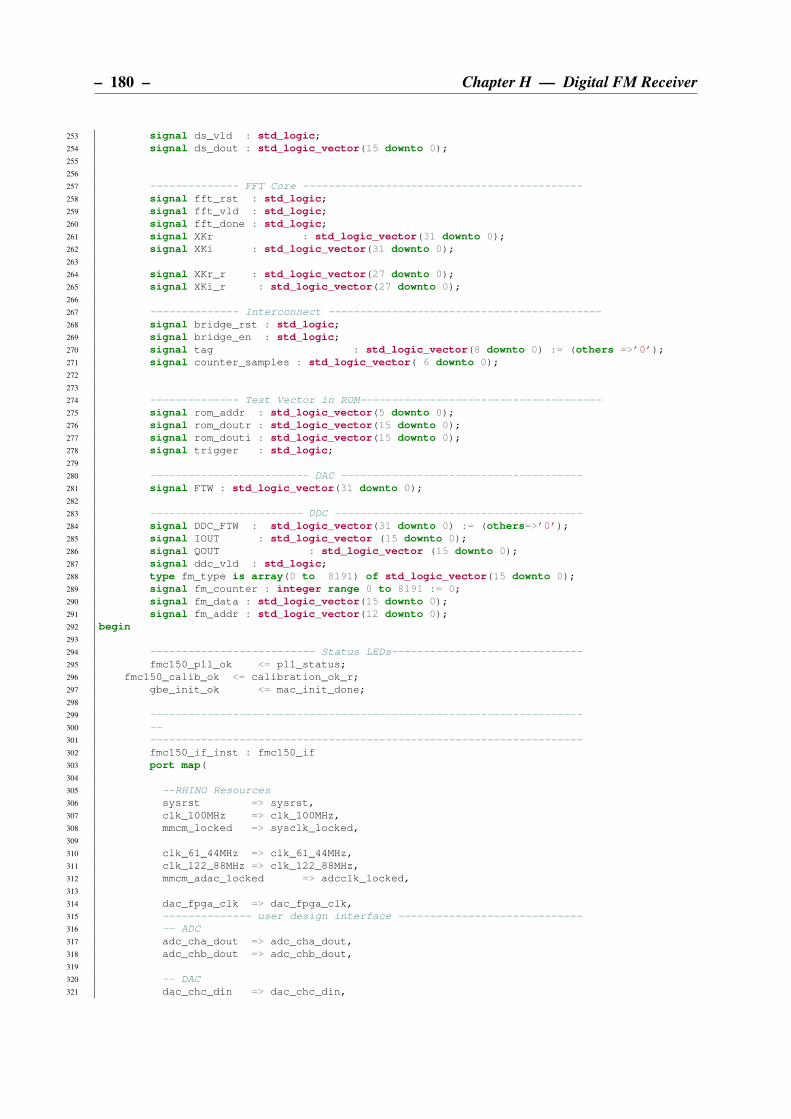
– 180 – Chapter H — Digital FM Receiver
253 signal ds_vld : std_logic;
254 signal ds_dout : std_logic_vector(15 downto 0);
255
256
257 -------------- FFT Core --------------------------------------------
258 signal fft_rst : std_logic;
259 signal fft_vld : std_logic;
260 signal fft_done : std_logic;
261 signal XKr : std_logic_vector(31 downto 0);
262 signal XKi : std_logic_vector(31 downto 0);
263
264 signal XKr_r : std_logic_vector(27 downto 0);
265 signal XKi_r : std_logic_vector(27 downto 0);
266
267 -------------- Interconnect -------------------------------------------
268 signal bridge_rst : std_logic;
269 signal bridge_en : std_logic;
270 signal tag : std_logic_vector(8 downto 0) := (others =>’0’);
271 signal counter_samples : std_logic_vector( 6 downto 0);
272
273
274 -------------- Test Vector in ROM--------------------------------------
275 signal rom_addr : std_logic_vector(5 downto 0);
276 signal rom_doutr : std_logic_vector(15 downto 0);
277 signal rom_douti : std_logic_vector(15 downto 0);
278 signal trigger : std_logic;
279
280 ------------------------- DAC --------------------------------------
281 signal FTW : std_logic_vector(31 downto 0);
282
283 ------------------------ DDC ---------------------------------------
284 signal DDC_FTW : std_logic_vector(31 downto 0) := (others=>’0’);
285 signal IOUT : std_logic_vector (15 downto 0);
286 signal QOUT : std_logic_vector (15 downto 0);
287 signal ddc_vld : std_logic;
288 type fm_type is array(0 to 8191) of std_logic_vector(15 downto 0);
289 signal fm_counter : integer range 0 to 8191 := 0;
290 signal fm_data : std_logic_vector(15 downto 0);
291 signal fm_addr : std_logic_vector(12 downto 0);
292 begin
293
294 -------------------------- Status LEDs------------------------------
295 fmc150_pll_ok <= pll_status;
296 fmc150_calib_ok <= calibration_ok_r;
297 gbe_init_ok <= mac_init_done;
298
299 --------------------------------------------------------------------
300 --
301 --------------------------------------------------------------------
302 fmc150_if_inst : fmc150_if
303 port map(
304
305 --RHINO Resources
306 sysrst => sysrst,
307 clk_100MHz => clk_100MHz,
308 mmcm_locked => sysclk_locked,
309
310 clk_61_44MHz => clk_61_44MHz,
311 clk_122_88MHz => clk_122_88MHz,
312 mmcm_adac_locked => adcclk_locked,
313
314 dac_fpga_clk => dac_fpga_clk,
315 -------------- user design interface -----------------------------
316 -- ADC
317 adc_cha_dout => adc_cha_dout,
318 adc_chb_dout => adc_chb_dout,
319
320 -- DAC
321 dac_chc_din => dac_chc_din,

Chapter H — Digital FM Receiver – 181 –
322 dac_chd_din => dac_chd_din,
323
324 calibration_ok => calibration_ok_r,
325
326 -------------- physical external interface -----------------------
327
328 --Clock/Data connection to ADC on FMC150 (ADS62P49)
329 clk_ab_p => clk_ab_p,
330 clk_ab_n => clk_ab_n,
331 cha_p => cha_p,
332 cha_n => cha_n,
333 chb_p => chb_p,
334 chb_n => chb_n,
335
336 --Clock/Data connection to DAC on FMC150 (DAC3283)
337 dac_dclk_p => dac_dclk_p,
338 dac_dclk_n => dac_dclk_n,
339 dac_data_p => dac_data_p,
340 dac_data_n => dac_data_n,
341 dac_frame_p => dac_frame_p,
342 dac_frame_n => dac_frame_n,
343 txenable => txenable,
344
345 --Clock/Trigger connection to FMC150
346 clk_to_fpga => clk_to_fpga,
347 ext_trigger => ext_trigger,
348
349 --Serial Peripheral Interface (SPI)
350 spi_sclk => spi_sclk,
351 spi_sdata => spi_sdata,
352
353 -- ADC specific signals
354 adc_n_en => adc_n_en,
355 adc_sdo => adc_sdo,
356 adc_reset => adc_reset,
357
358 -- CDCE specific signals
359 cdce_n_en => cdce_n_en,
360 cdce_sdo => cdce_sdo,
361 cdce_n_reset => cdce_n_reset,
362 cdce_n_pd => cdce_n_pd,
363 ref_en => ref_en,
364 pll_status => pll_status,
365
366 -- DAC specific signals
367 dac_n_en => dac_n_en,
368 dac_sdo => dac_sdo,
369
370 -- Monitoring specific signals
371 mon_n_en => mon_n_en,
372 mon_sdo => mon_sdo,
373 mon_n_reset => mon_n_reset,
374 mon_n_int => mon_n_int,
375
376 --FMC-0 Present status
377 nfmc0_prsnt => nfmc0_prsnt
378 );
379
380
381 --1Gbe Ethernet interface
382
383 UDP_1GbE_inst : UDP_1GbE
384 generic map(
385 UDP_TX_DATA_BYTE_LENGTH => UDP_TX_DATA_BYTE_LENGTH,
386 UDP_RX_DATA_BYTE_LENGTH => UDP_RX_DATA_BYTE_LENGTH
387 )
388 port map(
389 -- user logic interface
390 own_ip_addr => x"c0a80003",

– 182 – Chapter H — Digital FM Receiver
391 own_mac_addr => x"0024ba7d1d70",
392 dst_ip_addr => x"c0a80001",
393 dst_mac_addr => dst_mac_addr,
394
395 udp_src_port => x"26CA", --9930
396 udp_dst_port => x"26CA",
397
398 udp_tx_pkt_data => udp_tx_pkt_data,
399 udp_tx_pkt_vld => udp_tx_pkt_vld,
400 udp_tx_rdy => udp_tx_rdy,
401
402 udp_rx_pkt_data => udp_rx_pkt_data,
403 udp_rx_pkt_req => udp_rx_pkt_req,
404 udp_rx_rdy => udp_rx_rdy,
405
406 mac_init_done => mac_init_done,
407
408 -- MAC interface
409 GIGE_COL => GIGE_COL,
410 GIGE_CRS => GIGE_CRS,
411 GIGE_MDC => GIGE_MDC,
412 GIGE_MDIO => GIGE_MDIO,
413 GIGE_TX_CLK => GIGE_TX_CLK,
414 GIGE_nRESET => GIGE_nRESET,
415 GIGE_RXD => GIGE_RXD,
416 GIGE_RX_CLK => GIGE_RX_CLK,
417 GIGE_RX_DV => GIGE_RX_DV,
418 GIGE_RX_ER => GIGE_RX_ER,
419 GIGE_TXD => GIGE_TXD,
420 GIGE_GTX_CLK => GIGE_GTX_CLK,
421 GIGE_TX_EN => GIGE_TX_EN,
422 GIGE_TX_ER => GIGE_TX_ER,
423
424 -- system control
425 clk_125mhz => clk_125mhz,
426 clk_100mhz => clk_100mhz,
427 sys_rst_i => sysrst,
428 sysclk_locked => sysclk_locked
429 );
430
431 clk_manager_inst : clk_manager
432 port map(
433 --External Control
434 SYS_CLK_P_i => sys_clk_p,
435 SYS_CLK_N_i => sys_clk_n,
436 SYS_RST_i => SYS_RST_i,
437
438 clk_ab_p => clk_ab_p,
439 clk_ab_n => clk_ab_n,
440
441 -- Clock out ports
442 clk_125mhz => clk_125mhz,
443 clk_122_88mhz => clk_122_88mhz,
444 clk_100mhz => clk_100mhz,
445 clk_61_44mhz => clk_61_44mhz,
446 clk_25mhz => clk_25mhz,
447 -- Status and control signals
448 RESET => sysrst,
449 sysclk_locked => sysclk_locked,
450 adcclk_locked => adcclk_locked
451 );
452
453
454 --Digtal Down Converter
455
456 ddc_inst : ddc
457 generic map(
458 DIN_WIDTH => 16,
459 DOUT_WIDTH => 16,
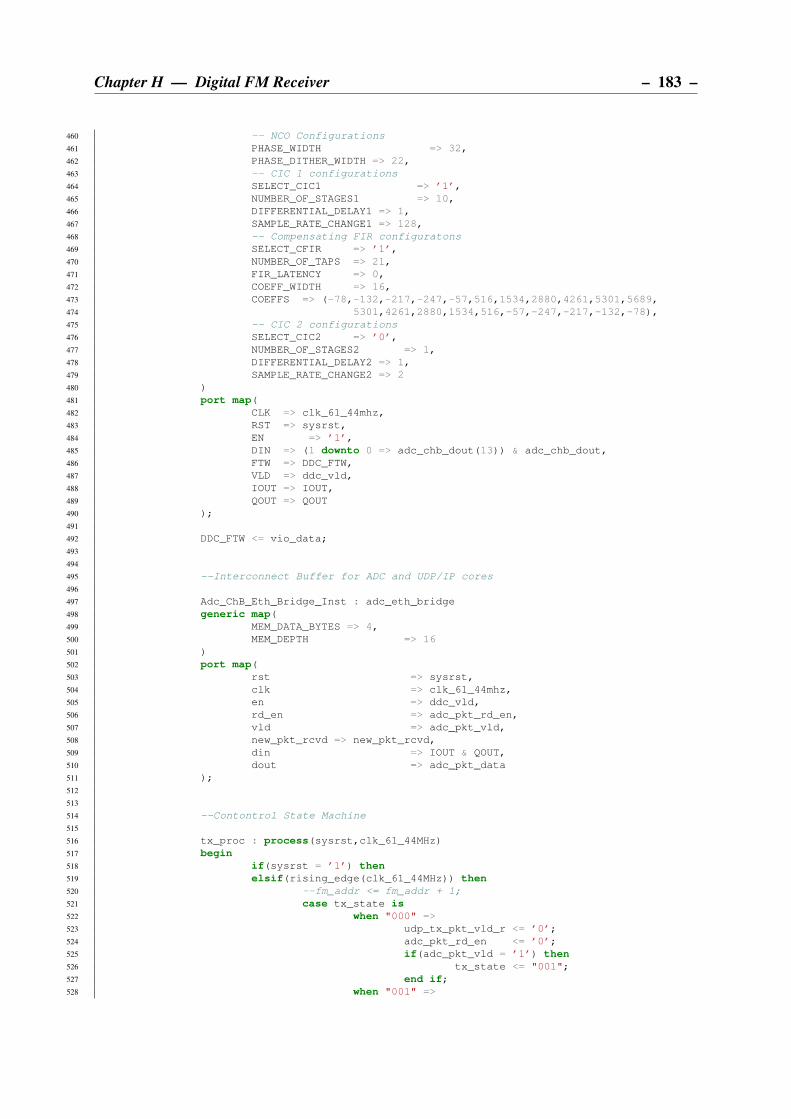
Chapter H — Digital FM Receiver – 183 –
460 -- NCO Configurations
461 PHASE_WIDTH => 32,
462 PHASE_DITHER_WIDTH => 22,
463 -- CIC 1 configurations
464 SELECT_CIC1 => ’1’,
465 NUMBER_OF_STAGES1 => 10,
466 DIFFERENTIAL_DELAY1 => 1,
467 SAMPLE_RATE_CHANGE1 => 128,
468 -- Compensating FIR configuratons
469 SELECT_CFIR => ’1’,
470 NUMBER_OF_TAPS => 21,
471 FIR_LATENCY => 0,
472 COEFF_WIDTH => 16,
473 COEFFS => (-78,-132,-217,-247,-57,516,1534,2880,4261,5301,5689,
474 5301,4261,2880,1534,516,-57,-247,-217,-132,-78),
475 -- CIC 2 configurations
476 SELECT_CIC2 => ’0’,
477 NUMBER_OF_STAGES2 => 1,
478 DIFFERENTIAL_DELAY2 => 1,
479 SAMPLE_RATE_CHANGE2 => 2
480 )
481 port map(
482 CLK => clk_61_44mhz,
483 RST => sysrst,
484 EN => ’1’,
485 DIN => (1 downto 0 => adc_chb_dout(13)) & adc_chb_dout,
486 FTW => DDC_FTW,
487 VLD => ddc_vld,
488 IOUT => IOUT,
489 QOUT => QOUT
490 );
491
492 DDC_FTW <= vio_data;
493
494
495 --Interconnect Buffer for ADC and UDP/IP cores
496
497 Adc_ChB_Eth_Bridge_Inst : adc_eth_bridge
498 generic map(
499 MEM_DATA_BYTES => 4,
500 MEM_DEPTH => 16
501 )
502 port map(
503 rst => sysrst,
504 clk => clk_61_44mhz,
505 en => ddc_vld,
506 rd_en => adc_pkt_rd_en,
507 vld => adc_pkt_vld,
508 new_pkt_rcvd => new_pkt_rcvd,
509 din => IOUT & QOUT,
510 dout => adc_pkt_data
511 );
512
513
514 --Contontrol State Machine
515
516 tx_proc : process(sysrst,clk_61_44MHz)
517 begin
518 if(sysrst = ’1’) then
519 elsif(rising_edge(clk_61_44MHz)) then
520 --fm_addr <= fm_addr + 1;
521 case tx_state is
522 when "000" =>
523 udp_tx_pkt_vld_r <= ’0’;
524 adc_pkt_rd_en <= ’0’;
525 if(adc_pkt_vld = ’1’) then
526 tx_state <= "001";
527 end if;
528 when "001" =>
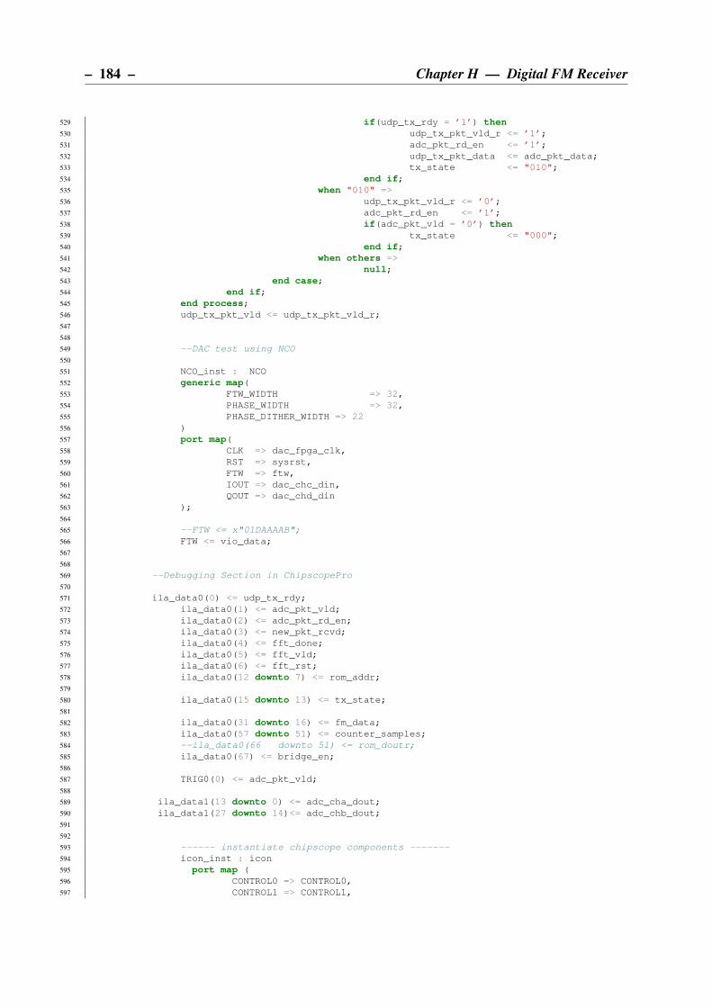
– 184 – Chapter H — Digital FM Receiver
529 if(udp_tx_rdy = ’1’) then
530 udp_tx_pkt_vld_r <= ’1’;
531 adc_pkt_rd_en <= ’1’;
532 udp_tx_pkt_data <= adc_pkt_data;
533 tx_state <= "010";
534 end if;
535 when "010" =>
536 udp_tx_pkt_vld_r <= ’0’;
537 adc_pkt_rd_en <= ’1’;
538 if(adc_pkt_vld = ’0’) then
539 tx_state <= "000";
540 end if;
541 when others =>
542 null;
543 end case;
544 end if;
545 end process;
546 udp_tx_pkt_vld <= udp_tx_pkt_vld_r;
547
548
549 --DAC test using NCO
550
551 NCO_inst : NCO
552 generic map(
553 FTW_WIDTH => 32,
554 PHASE_WIDTH => 32,
555 PHASE_DITHER_WIDTH => 22
556 )
557 port map(
558 CLK => dac_fpga_clk,
559 RST => sysrst,
560 FTW => ftw,
561 IOUT => dac_chc_din,
562 QOUT => dac_chd_din
563 );
564
565 --FTW <= x"01DAAAAB";
566 FTW <= vio_data;
567
568
569 --Debugging Section in ChipscopePro
570
571 ila_data0(0) <= udp_tx_rdy;
572 ila_data0(1) <= adc_pkt_vld;
573 ila_data0(2) <= adc_pkt_rd_en;
574 ila_data0(3) <= new_pkt_rcvd;
575 ila_data0(4) <= fft_done;
576 ila_data0(5) <= fft_vld;
577 ila_data0(6) <= fft_rst;
578 ila_data0(12 downto 7) <= rom_addr;
579
580 ila_data0(15 downto 13) <= tx_state;
581
582 ila_data0(31 downto 16) <= fm_data;
583 ila_data0(57 downto 51) <= counter_samples;
584 --ila_data0(66 downto 51) <= rom_doutr;
585 ila_data0(67) <= bridge_en;
586
587 TRIG0(0) <= adc_pkt_vld;
588
589 ila_data1(13 downto 0) <= adc_cha_dout;
590 ila_data1(27 downto 14)<= adc_chb_dout;
591
592
593 ------ instantiate chipscope components -------
594 icon_inst : icon
595 port map (
596 CONTROL0 => CONTROL0,
597 CONTROL1 => CONTROL1,

Chapter H — Digital FM Receiver – 185 –
598 CONTROL2 => CONTROL2
599 );
600
601 ila_data0_inst : ila0
602 port map (
603 CONTROL => CONTROL0,
604 CLK => clk_100MHz,--clk_245_76MHz,
605 DATA => ila_data0,
606 TRIG0 => TRIG0);
607
608 ila_data1_inst : ila1
609 port map (
610 CONTROL => CONTROL2,
611 CLK => clk_61_44MHz,
612 DATA => ila_data1,
613 TRIG0 => TRIG1);
614
615 vio_inst : vio
616 port map (
617 CONTROL => CONTROL1,
618 ASYNC_OUT => vio_data);
619 --------------------------------------------------------------------
620 -- End
621 --------------------------------------------------------------------
622 end Behavioral;
H.2 FM DEMODULATION FUNCTION IN MATLAB [84]
1 function [y_FM_demodulated] = FM_IQ_Demod(y)
2 %This function demodualtes an FM signal. It is assumed that the FM signal
3 %is complex (e.g. an IQ signal) centered at DC and occupies less than 90%
4 %of total bandwidth.
5
6
7 %filter design!
8 b = firls(30,[0 .9],[0 1],’differentiator’); %design differentiater
9 d=y./abs(y);%normalize the amplitude (i.e. remove amplitude variations)
10 rd=real(d); %real part of normalized siganl.
11 id=imag(d); %imaginary part of normalized signal.
12 y_FM_demodulated=(rd.*conv(id,b,’same’)-id.*conv(rd,b,’same’))./(rd.ˆ2+id.ˆ2);%demodulate!
13
14 end
H.3 PLOTTING THE FPGA RESULTS IN MATLAB
1 % ----------------------------------------------------------------------
2 % This plots FPGA results using data files containing FM samples captured
3 % using UDP.
4 % ----------------------------------------------------------------------
5 Fs = 122.88e6/128;
6
7 %--------------------- 89.0MHz FM station ------------------------------
8 fpgaOutRaw = dlmread(’89.0/udp_capture’,’ ’);
9 fpgaout = complex(fpgaOutRaw(:,1),fpgaOutRaw(:,2));
10
11 N = length(fpgaout);
12 NFFT = N;
13 f1 = fftshift(fft(fpgaout,NFFT));
14 F1 = abs(f1)/N;
15 f = Fs*(-NFFT/2:NFFT/2-1)/NFFT;
16
17 subplot(3,2,1);
18 plot(f/1e3,F1,’k’);
19 title(’Spectrum of 89.0MHz FM station (DDC core output)’);

– 186 – Chapter H — Digital FM Receiver
20 xlabel(’Frequency ($kHz$)’);
21 ylabel(’Magnitude’); grid on;
22 %xlim([-1e6,1e6]);
23
24 [fm_demod_signal] = FM_IQ_Demod(fpgaout);
25 f2 = fftshift(fft(fm_demod_signal,NFFT));
26 F2 = abs(f2)/N;
27
28 subplot(3,2,2);
29 plot(f/1e3,F2,’k’);
30 title(’Spectrum of FM demodulated 89.0MHz FM station in MATLAB’);
31 xlabel(’Frequency ($kHz$)’);
32 ylabel(’Magnitude’);
33 xlim([0,70]);grid on;
34
35 %--------------------- 94.5MHz FM station -----------------------------
36 fpgaOutRaw = dlmread(’94.5/udp_capture’,’ ’);
37 fpgaout = complex(fpgaOutRaw(:,1),fpgaOutRaw(:,2));
38
39 N = length(fpgaout);
40 NFFT = N;
41 f1 = fftshift(fft(fpgaout,NFFT));
42 F1 = abs(f1)/N;
43 f = Fs*(-NFFT/2:NFFT/2-1)/NFFT;
44
45 subplot(3,2,3);
46 plot(f/1e3,F1,’k’);
47 title(’Spectrum of 94.5MHz FM station (DDC core output)’);
48 xlabel(’Frequency ($kHz$)’);
49 ylabel(’Magnitude’); grid on;
50 %xlim([-1e6,1e6]);
51
52 [fm_demod_signal] = FM_IQ_Demod(fpgaout);
53 f2 = fftshift(fft(fm_demod_signal,NFFT));
54 F2 = abs(f2)/N;
55
56 subplot(3,2,4);
57 plot(f/1e3,F2,’k’);
58 title(’Spectrum of FM demodulated 94.5MHz FM station in MATLAB’);
59 xlabel(’Frequency ($kHz$)’);
60 ylabel(’Magnitude’);
61 xlim([0,70]);grid on;
62
63 %--------------------- 95.3MHz FM station ------------------------------
64 fpgaOutRaw = dlmread(’95.3/udp_capture’,’ ’);
65 fpgaout = complex(fpgaOutRaw(:,1),fpgaOutRaw(:,2));
66
67 N = length(fpgaout);
68 NFFT = N;
69 f1 = fftshift(fft(fpgaout,NFFT));
70 F1 = abs(f1)/N;
71 f = Fs*(-NFFT/2:NFFT/2-1)/NFFT;
72
73 subplot(3,2,5);
74 plot(f/1e3,F1,’k’);
75 title(’Spectrum of 95.3MHz FM station (DDC core output)’);
76 xlabel(’Frequency ($kHz$)’);
77 ylabel(’Magnitude’); grid on;
78
79 [fm_demod_signal] = FM_IQ_Demod(fpgaout);
80 f2 = fftshift(fft(fm_demod_signal,NFFT));
81 F2 = abs(f2)/N;
82
83 subplot(3,2,6);
84 plot(f/1e3,F2,’k’);
85 title(’Spectrum of FM demodulated 95.3MHz FM station in MATLAB’);
86 xlabel(’Frequency ($kHz$)’);
87 ylabel(’Magnitude’);
88 xlim([0,70]);grid on;